JP6845173B2 - Image processing device and image processing method - Google Patents
Image processing device and image processing method Download PDFInfo
- Publication number
- JP6845173B2 JP6845173B2 JP2018048345A JP2018048345A JP6845173B2 JP 6845173 B2 JP6845173 B2 JP 6845173B2 JP 2018048345 A JP2018048345 A JP 2018048345A JP 2018048345 A JP2018048345 A JP 2018048345A JP 6845173 B2 JP6845173 B2 JP 6845173B2
- Authority
- JP
- Japan
- Prior art keywords
- pixel
- correction
- pixels
- output
- output buffer
- Prior art date
- Legal status (The legal status is an assumption and is not a legal conclusion. Google has not performed a legal analysis and makes no representation as to the accuracy of the status listed.)
- Active
Links
- 238000012545 processing Methods 0.000 title claims description 37
- 238000003672 processing method Methods 0.000 title claims description 4
- 239000000872 buffer Substances 0.000 claims description 214
- 238000012937 correction Methods 0.000 claims description 124
- 230000005540 biological transmission Effects 0.000 claims description 54
- 238000004364 calculation method Methods 0.000 claims description 48
- 238000012546 transfer Methods 0.000 claims description 12
- 238000000034 method Methods 0.000 description 21
- 230000003287 optical effect Effects 0.000 description 16
- 230000006870 function Effects 0.000 description 12
- 238000003384 imaging method Methods 0.000 description 11
- 238000010586 diagram Methods 0.000 description 9
- 230000004075 alteration Effects 0.000 description 6
- 238000006243 chemical reaction Methods 0.000 description 6
- 238000012805 post-processing Methods 0.000 description 6
- 238000005516 engineering process Methods 0.000 description 4
- 238000003702 image correction Methods 0.000 description 4
- 238000004519 manufacturing process Methods 0.000 description 4
- 239000000470 constituent Substances 0.000 description 3
- 230000000694 effects Effects 0.000 description 3
- 238000011156 evaluation Methods 0.000 description 3
- 230000007423 decrease Effects 0.000 description 2
- 239000000463 material Substances 0.000 description 2
- 230000002093 peripheral effect Effects 0.000 description 2
- 238000004088 simulation Methods 0.000 description 2
- 238000013461 design Methods 0.000 description 1
- 239000000284 extract Substances 0.000 description 1
- 238000010191 image analysis Methods 0.000 description 1
- 230000002265 prevention Effects 0.000 description 1
- 230000000717 retained effect Effects 0.000 description 1
- 230000009466 transformation Effects 0.000 description 1
Images


Classifications
-
- G—PHYSICS
- G06—COMPUTING; CALCULATING OR COUNTING
- G06T—IMAGE DATA PROCESSING OR GENERATION, IN GENERAL
- G06T5/00—Image enhancement or restoration
- G06T5/80—Geometric correction
-
- H—ELECTRICITY
- H04—ELECTRIC COMMUNICATION TECHNIQUE
- H04N—PICTORIAL COMMUNICATION, e.g. TELEVISION
- H04N23/00—Cameras or camera modules comprising electronic image sensors; Control thereof
- H04N23/60—Control of cameras or camera modules
-
- H—ELECTRICITY
- H04—ELECTRIC COMMUNICATION TECHNIQUE
- H04N—PICTORIAL COMMUNICATION, e.g. TELEVISION
- H04N23/00—Cameras or camera modules comprising electronic image sensors; Control thereof
- H04N23/80—Camera processing pipelines; Components thereof
- H04N23/81—Camera processing pipelines; Components thereof for suppressing or minimising disturbance in the image signal generation
-
- H—ELECTRICITY
- H04—ELECTRIC COMMUNICATION TECHNIQUE
- H04N—PICTORIAL COMMUNICATION, e.g. TELEVISION
- H04N25/00—Circuitry of solid-state image sensors [SSIS]; Control thereof
- H04N25/60—Noise processing, e.g. detecting, correcting, reducing or removing noise
-
- G—PHYSICS
- G06—COMPUTING; CALCULATING OR COUNTING
- G06T—IMAGE DATA PROCESSING OR GENERATION, IN GENERAL
- G06T1/00—General purpose image data processing
- G06T1/60—Memory management
-
- G—PHYSICS
- G06—COMPUTING; CALCULATING OR COUNTING
- G06T—IMAGE DATA PROCESSING OR GENERATION, IN GENERAL
- G06T3/00—Geometric image transformations in the plane of the image
- G06T3/04—Context-preserving transformations, e.g. by using an importance map
- G06T3/047—Fisheye or wide-angle transformations
-
- H—ELECTRICITY
- H04—ELECTRIC COMMUNICATION TECHNIQUE
- H04N—PICTORIAL COMMUNICATION, e.g. TELEVISION
- H04N23/00—Cameras or camera modules comprising electronic image sensors; Control thereof
- H04N23/80—Camera processing pipelines; Components thereof
-
- H—ELECTRICITY
- H04—ELECTRIC COMMUNICATION TECHNIQUE
- H04N—PICTORIAL COMMUNICATION, e.g. TELEVISION
- H04N25/00—Circuitry of solid-state image sensors [SSIS]; Control thereof
- H04N25/40—Extracting pixel data from image sensors by controlling scanning circuits, e.g. by modifying the number of pixels sampled or to be sampled
-
- H—ELECTRICITY
- H04—ELECTRIC COMMUNICATION TECHNIQUE
- H04N—PICTORIAL COMMUNICATION, e.g. TELEVISION
- H04N25/00—Circuitry of solid-state image sensors [SSIS]; Control thereof
- H04N25/70—SSIS architectures; Circuits associated therewith
- H04N25/71—Charge-coupled device [CCD] sensors; Charge-transfer registers specially adapted for CCD sensors
- H04N25/75—Circuitry for providing, modifying or processing image signals from the pixel array
-
- H—ELECTRICITY
- H04—ELECTRIC COMMUNICATION TECHNIQUE
- H04N—PICTORIAL COMMUNICATION, e.g. TELEVISION
- H04N25/00—Circuitry of solid-state image sensors [SSIS]; Control thereof
- H04N25/70—SSIS architectures; Circuits associated therewith
- H04N25/76—Addressed sensors, e.g. MOS or CMOS sensors
-
- H—ELECTRICITY
- H04—ELECTRIC COMMUNICATION TECHNIQUE
- H04N—PICTORIAL COMMUNICATION, e.g. TELEVISION
- H04N9/00—Details of colour television systems
- H04N9/64—Circuits for processing colour signals
- H04N9/68—Circuits for processing colour signals for controlling the amplitude of colour signals, e.g. automatic chroma control circuits
- H04N9/69—Circuits for processing colour signals for controlling the amplitude of colour signals, e.g. automatic chroma control circuits for modifying the colour signals by gamma correction
Landscapes
- Engineering & Computer Science (AREA)
- Multimedia (AREA)
- Signal Processing (AREA)
- Physics & Mathematics (AREA)
- General Physics & Mathematics (AREA)
- Theoretical Computer Science (AREA)
- Image Processing (AREA)
- Image Input (AREA)
- Geometry (AREA)
Description
本発明の実施形態は、画像処理装置及び画像処理方法に関する。 Embodiments of the present invention relate to an image processing apparatus and an image processing method.
一般的に、デジタルカメラ等の撮像装置で被写体を撮像して得られた画像は、撮像レンズ等の光学系が有する歪曲収差や倍率色収差の影響を受ける。例えば、撮像装置によって取得した画像を、自動車の衝突防止等に利用したり監視カメラに利用したりする場合等においては、その目的から超広角レンズが採用されることがあり、歪曲収差や倍率色収差が大きくなる傾向にある。 Generally, an image obtained by imaging a subject with an imaging device such as a digital camera is affected by distortion and chromatic aberration of magnification of an optical system such as an imaging lens. For example, when an image acquired by an imaging device is used for vehicle collision prevention or a surveillance camera, an ultra-wide-angle lens may be used for that purpose, and distortion or chromatic aberration of magnification may occur. Tends to increase.
歪曲収差を抑制するためには、レンズの材質を工夫したり、非球面レンズを用いたりするが、設計や製造のコストが増大するという問題がある。また、倍率色収差を抑制するためには、屈折率の異なる素材のレンズの組を多数使用するためにレンズ数が多くなり、装置の大型化や製造コストが増大してしまうという問題がある。 In order to suppress distortion, the material of the lens is devised or an aspherical lens is used, but there is a problem that the design and manufacturing costs increase. Further, in order to suppress chromatic aberration of magnification, there is a problem that the number of lenses is increased because a large number of sets of lenses made of materials having different refractive indexes are used, which increases the size of the apparatus and the manufacturing cost.
そこで、近年では、これらの問題を解決するものとして、歪曲収差や倍率色収差によって画像に歪みなどが生じる場合、画像に対して電気的に、光学系で生じる歪みを補正する画像処理装置が用いられている。 Therefore, in recent years, as a solution to these problems, when distortion occurs in an image due to distortion or chromatic aberration of magnification, an image processing device that electrically corrects the distortion generated in the optical system is used for the image. ing.
従来の画像処理装置における電気的補正方法では、補正後の出力画素をラスタスキャン順に出力するため、出力画素位置から補正に必要な入力画素位置を計算していた。ところが、画像の歪みが大きい場合、出力画素位置と入力画素位置に大きなずれが生じる。従って、多数のラインバッファを用意して入力画素を保持しておく必要があるため、装置が大型化してしまう。また、一般的に、ラインバッファはSRAMで構成されるが、SRAMは高価であるため、製造コストが高くなってしまうという問題がある。 In the electrical correction method in the conventional image processing apparatus, since the output pixels after correction are output in the order of raster scan, the input pixel position required for correction is calculated from the output pixel position. However, when the distortion of the image is large, a large deviation occurs between the output pixel position and the input pixel position. Therefore, it is necessary to prepare a large number of line buffers to hold the input pixels, which increases the size of the device. Further, generally, the line buffer is composed of SRAM, but since SRAM is expensive, there is a problem that the manufacturing cost becomes high.
実施形態は、バッファメモリ容量の低減及び伝送効率の向上を図ることができる画像処理装置及び画像処理方法を提供することを目的とする。 An object of the embodiment is to provide an image processing apparatus and an image processing method capable of reducing the buffer memory capacity and improving the transmission efficiency.
実施の形態の画像処理装置は、入力画像を構成する複数の画素がラスタスキャン順に入力され、前記入力画像の歪に基づいて前記画素の位置を補正する補正演算を行って補正画素を求めるものであって、前記入力される画素の位置である入力画素位置から出力する画素の位置である補正画素位置を求める第1の演算、前記補正画素位置及びその周辺の複数画素の画素位置に対応する前記入力画像の画素位置を求める第2の演算、前記入力画像の画素位置に対応する前記補正画素を求める第3の演算を含む前記補正演算を行い、前記第1の演算の結果得られた補正画素位置の情報を前記補正画素に付加して、前記補正画素位置の情報が付加された前記補正画素を出力する歪補正回路と、前記歪補正回路の出力が前記補正画素位置の情報に基づくランダム順に入力される出力バッファであって、前記補正画素位置が連続する補正画素の集合である伝送ブロック毎に補正画素を出力する2段以上に階層化された複数の出力バッファと、前記歪補正回路の出力画素を、前記複数の出力バッファのうち初段の出力バッファに書き込むと共に、書き込んだ画素を後段の出力バッファに順次転送するものであって、各段の出力バッファに前記伝送ブロックを分割したサブブロックを記憶させるコントローラとを具備する。 The image processing apparatus of the embodiment, a plurality of pixels constituting the input image is input to the raster scan order to determine the corrected pixel I line correction operation for correcting the position of the pixel based on the distortion of the input image The first calculation for obtaining the correction pixel position, which is the position of the output pixel from the input pixel position, which is the position of the input pixel, corresponds to the correction pixel position and the pixel positions of a plurality of pixels around the correction pixel position. The correction calculation including the second calculation for obtaining the pixel position of the input image and the third calculation for obtaining the correction pixel corresponding to the pixel position of the input image is performed , and the correction obtained as a result of the first calculation is performed. It adds information of the pixel position in the corrected pixel, and distortion correction circuit for outputting the corrected pixel information of the corrected pixel position is added, the random output of the distortion correction circuit is based on the information of the corrected pixel position A plurality of output buffers that are sequentially input and are layered in two or more stages for outputting correction pixels for each transmission block, which is a set of correction pixels in which the correction pixel positions are continuous, and the distortion correction circuit. The output pixels of the above are written to the output buffer of the first stage among the plurality of output buffers, and the written pixels are sequentially transferred to the output buffer of the subsequent stage, and the transmission block is divided into the output buffers of each stage. It includes a controller for storing blocks.
以下、図面を参照して本発明の実施の形態について詳細に説明する。 Hereinafter, embodiments of the present invention will be described in detail with reference to the drawings.
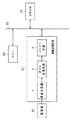
図1は本発明の一実施の形態に係る画像処理装置を示すブロック図である。本実施の形態は歪補正処理においてラインバッファ容量を低減するラスタスキャン入力・ランダム出力を採用する。本実施の形態はこのラスタスキャン入力・ランダム出力の歪補正に際して、出力バッファを多層化することにより、バッファサイズ(容量)の低減及び伝送効率の向上を可能にするものである。 FIG. 1 is a block diagram showing an image processing apparatus according to an embodiment of the present invention. This embodiment employs raster scan input / random output that reduces the line buffer capacity in distortion correction processing. The present embodiment makes it possible to reduce the buffer size (capacity) and improve the transmission efficiency by forming the output buffer in multiple layers when correcting the distortion of the raster scan input / random output.
図1の画像処理装置は、CPU25を備えている。CPU25は図示しないメモリに記憶されたプログラムに従って動作して各部を制御するようになっている。撮像部22は、CMOSセンサ等の図示しない撮像素子を備えている。撮像部22は、図示しない光学系を介して入射した光学像を撮像素子によって光電変換することで、撮像信号(撮像画像)を取得する。撮像部22の出力(撮像画像)は画像処理回路21に与えられ、画像処理回路21によって歪補正された後、バス23を介してDRAM24に与えられて記憶されるようになっている。撮像部22からの撮像画像は光学系の歪曲収差等による歪みを有しており、画像処理回路21は、歪曲収差の補正等の各種画像処理を行う。
The image processing device of FIG. 1 includes a
撮像部22からのラスタスキャン順の撮像出力は画像処理回路21を構成する歪補正回路1に入力される。歪補正回路1は、入力された撮像画像に対して歪補正及び倍率色収差補正を行ってポスト処理回路2に出力する。ポスト処理回路2は、入力された画像に対してガンマ補正及び色空間補正を行った後バッファ回路3に出力する。バッファ回路3は、入力された画像を一時保持した後、バス23を介してDRAM24に出力する。こうして、DRAM24には、歪補正された画像が記憶される。
The image pickup output from the
ところで、上述したように、関連技術の歪補正では、ラスタスキャン順に入力された撮像出力をラインバッファに一旦蓄積し、ラスタスキャン出力順に順次DRAMへの書き込みを行う。関連技術における歪補正回路は、ラスタ順の出力(ラスタスキャン出力)に際して、当該出力画素が歪を受けなければあるべき本来の画素位置を求め、求めた画素位置の画素をラインバッファから読み出してDRAMに転送する。関連技術のラスタスキャン入力・ラスタスキャン出力では、画素出力に際して求めた画素位置の画素をラインバッファに格納しておく必要があり、ラインバッファとして歪の大きさに対応した十分な容量を確保しておく必要がある。 By the way, as described above, in the distortion correction of the related technology, the imaging outputs input in the order of raster scan are temporarily stored in the line buffer, and the images are sequentially written to the DRAM in the order of raster scan output. The distortion correction circuit in the related technology finds the original pixel position where the output pixel should not be distorted at the time of output in raster order (raster scan output), reads the pixel at the obtained pixel position from the line buffer, and DRAM. Transfer to. In the raster scan input and raster scan output of related technologies, it is necessary to store the pixels at the pixel positions obtained at the time of pixel output in the line buffer, and secure a sufficient capacity as a line buffer corresponding to the magnitude of distortion. Need to keep.
そこで、本実施の形態においては、ラスタスキャン入力・ランダム出力を採用することでラインバッファを削減する歪補正処理を採用する。本実施の形態において採用するラスタスキャン入力・ランダム出力では、入力された画素を、当該画素が歪を受けなければあるべき本来の画素位置(以下、補正画素位置という)に対応するDRAMのアドレスに格納するように制御を行う。従って、ラインバッファとして比較的少ない容量のものを採用することができる。 Therefore, in the present embodiment, a distortion correction process that reduces the line buffer by adopting a raster scan input / random output is adopted. In the raster scan input / random output adopted in the present embodiment, the input pixel is set to the address of the DRAM corresponding to the original pixel position (hereinafter referred to as the corrected pixel position) that the pixel should not be distorted. Control to store. Therefore, a line buffer having a relatively small capacity can be adopted.
まず、図2及び図3を参照して、本実施の形態において採用するラスタスキャン入力・ランダム出力の歪補正処理を具体的に説明する。 First, with reference to FIGS. 2 and 3, the distortion correction processing of the raster scan input / random output adopted in the present embodiment will be specifically described.
図2は図1中の歪補正回路1の具体的な構成の一例を示すブロック図である。
FIG. 2 is a block diagram showing an example of a specific configuration of the
図2において、歪補正回路1は、ラインバッファ11と、書き込み画素位置計算部12と、読み出し画素位置計算部13と、書き込み画素位置判定部14と、パラメータ格納部15と、画素補間部16とから主に構成されている。
In FIG. 2, the
ラインバッファ11は、撮像部22からラスタスキャン順に読み込まれる入力画像の画素(入力画素)を、補正処理に必要なライン数だけ保持する。例えば、バイリニア補間を用いて歪曲収差の補正を行う場合、1〜2ライン分の画素を保持する。
The
書き込み画素位置計算部12は、補正対象である読み出し画素Piを用いて補間した画素が含まれると推定される、書き込み画素領域を算出する。具体的には、読み出し画素Piの位置(vo, ho)(以下、画素Pi(vo, ho)と示す)を含む、周辺4点の画素{Pi0(vo, ho)、Pi1(vo, ho-1)、Pi2(vo-1, ho-1)、Pi3(vo-1, ho)}からなる読み出し画素位置集合を定義する。なお、本説明において、画素位置座標(v, h)は、画像左上を原点(0, 0)として、vを垂直画素位置、hを水平画素位置としている。
The write pixel
読み出し画素Pi0、Pi1、Pi2、Pi3のそれぞれについて、画素位置計算の関数を用い、対応する書き込み画素Po0、Po1、Po2、Po3の位置(vo’, ho’)、(vo’, ho-1’)、(vo-1’, ho-1’)、(vo-1’, ho’)を算出する。4点の画素Po0(vo’, ho’)、Po1(vo’, ho-1’)、Po2(vo-1’, ho-1’)、Po3(vo-1’, ho’)を頂点とする矩形領域が、書き込み画素領域となる。 For each of the read pixels Pi0, Pi1, Pi2, and Pi3, the corresponding write pixel Po0, Po1, Po2, Po3 positions (vo', ho'), (vo', ho-1') are used using the pixel position calculation function. ), (Vo-1', ho-1'), (vo-1', ho') are calculated. Four pixels Po0 (vo', ho'), Po1 (vo', ho-1'), Po2 (vo-1', ho-1'), Po3 (vo-1', ho') are the vertices The rectangular area to be written becomes the writing pixel area.
画素位置計算には、例えば、多項式で表現される関数や、グリッドテーブル変換など、一般的な画素位置計算用の関数を用いることができる。ただし、画素位置計算関数は、逆関数が存在するものを用いる。 For the pixel position calculation, for example, a function expressed by a polynomial or a general pixel position calculation function such as a grid table transformation can be used. However, as the pixel position calculation function, a function having an inverse function is used.
読み出し画素位置計算部13は、書き込み画素領域内において、垂直位置、水平位置ともに整数となる画素の位置(書き込み画素候補Poc(v’, h’))を抽出する。そして、書き込み画素候補Poc(v’, h’)に対応する読み出し画素Pi(v”, h”)を、画素位置計算を行って算出する。なお、画素位置計算は、書き込み画素位置計算部12で行った画素位置計算の逆関数を用いて行う。候補が複数ある場合は、全ての候補Poc(v’, h’)に対して読み出し画素Pi(v”, h”)を算出する。
The read pixel
書き込み画素位置判定部14は、読み出し画素Pi(v”, h”)が集合に含まれている場合、当該画素Pi(v”, h”)に対する書き込み画素候補Poc(v’, h’)を、補正画素位置の書き込み画素Po(v’, h’)として確定する。
When the read pixel Pi (v ", h") is included in the set, the write pixel
パラメータ格納部15は、書き込み画素位置計算部12および読み出し画素位置計算部13における画素位置計算関数に用いるパラメータが格納されている。
The
画素補間部16は、確定した書き込み画素Po(v’, h’)に対応する読み出し画素Pi(v”, h”)の画素値を算出する。通常、読み出し画素Pi(v”, h”)の座標は非整数であるので、例えば周辺の4画素を用いたバイリニア補間など、既存の補間手法を用いて画素値を算出する。書き込み画素Po(v’, h’)の画素値として、算出した画素値を出力する。出力された画素値は、DRAMなどのメモリ(図示せず)に格納される。なお、出力画素は補正を行った順に出力するため、出力画素の位置(補正画素位置)はランダムとなる。
The
次に、歪補正回路1における画像補正処理の手順を説明する。図3は画像補正処理を説明するためのフローチャートである。
Next, the procedure of the image correction processing in the
まず、ラスタスキャン順に歪補正回路1に入力された画素を、ラインバッファ11に拡充する(S1)。ラインバッファ11には、画素補間部16での処理に必要なライン数分、入力画素を格納する。例えば、バイリニア補間を用いる場合、補間対象画素の周辺2×2画素(4画素)の画素値が必要となるため、少なくとも1ライン+1画素分の画素値を格納する。
First, the pixels input to the
次に、補正対象画素である読み出し画素Pi(vo, ho)を特定し、読み出し画素Piを用いて補間した画素が含まれると推定される、書き込み画素領域を算出する(S2)。具体的には、まず、読み出し画素Pi(vo, ho)を含む周囲4点の画素{Pi0(vo, ho)、Pi1(vo, ho-1)、Pi2(vo-1, ho-1)、Pi3(vo-1, ho)}からなる集合を定義する。すなわち、Pi1(vo, ho-1)は、Pi(vo, ho)の左隣の画素、Pi2(vo-1, ho-1)はPi(vo, ho)の左上の画素、Pi3(vo-1, ho)はPi(vo, ho)の上の画素である。次に、画素Pi0、Pi1、Pi2、Pi3のそれぞれについて、画素位置計算を行い、対応する書き込み画素Po0(vo’, ho’)、Po1(vo’, ho-1’)、Po2(vo-1’, ho-1’)、Po3(vo-1’, ho’)を算出する。 Next, the read pixel Pi (vo, ho), which is the correction target pixel, is specified, and the write pixel area estimated to include the pixel interpolated using the read pixel Pi is calculated (S2). Specifically, first, four surrounding pixels including the read pixel Pi (vo, ho) {Pi0 (vo, ho), Pi1 (vo, ho-1), Pi2 (vo-1, ho-1), Define a set consisting of Pi3 (vo-1, ho)}. That is, Pi1 (vo, ho-1) is the pixel to the left of Pi (vo, ho), Pi2 (vo-1, ho-1) is the upper left pixel of Pi (vo, ho), and Pi3 (vo-). 1, ho) is the pixel above Pi (vo, ho). Next, pixel position calculation is performed for each of the pixels Pi0, Pi1, Pi2, and Pi3, and the corresponding writing pixels Po0 (vo', ho'), Po1 (vo', ho-1'), and Po2 (vo-1) are performed. ', ho-1'), Po3 (vo-1', ho') are calculated.
画素位置計算は、例えば、多項式で表現される関数を用いる場合、次の手順で行う。
(a)像高の算出:入力画素の位置を、左上を原点とする(v, h)の座標系から、光学中心を原点とする(x, y)の座標系に変換する。なお、両座標系とも、水平方向は右側を正とし、垂直方向は下側を正とする。また、光学中心から入力画素までの距離(像高)rを算出する。以下に示す(1)〜(3)式を用いて行う。

(A) Calculation of image height: The position of the input pixel is converted from the coordinate system with the upper left as the origin (v, h) to the coordinate system with the optical center as the origin (x, y). In both coordinate systems, the right side is positive in the horizontal direction and the lower side is positive in the vertical direction. In addition, the distance (image height) r from the optical center to the input pixel is calculated. This is performed using the following equations (1) to (3).
(1)式において、vin は、垂直方向の入力画素位置(非負数)、[SENSOR_CROP_OFS_V]は、光学中心からの垂直画素位置オフセット(光学中心と、(v, h)座標系の原点との間の、垂直方向のオフセット)とする。また、(2)式において、hinは、水平方向の入力画素位置(非負数)、[SENSOR_CROP_OFS_H]は、光学中心からの水平画素位置オフセット(光学中心と、(v, h)座標系の原点との間の、水平方向のオフセット)とする。また、(3)式において、[NORM_SCALE]は正規化係数(非負数)とする。 In equation (1), v in is the vertical input pixel position (non-negative number), and [SENSOR_CROP_OFS_V] is the vertical pixel position offset from the optical center (optical center and the origin of the (v, h) coordinate system. Between, the vertical offset). In equation (2), h in is the horizontal input pixel position (non-negative number), and [SENSOR_CROP_OFS_H] is the horizontal pixel position offset from the optical center (optical center and origin of the (v, h) coordinate system. Horizontal offset between and). Further, in Eq. (3), [NORM_SCALE] is a normalizing coefficient (non-negative number).
なお、画像中心と光学中心とが一致する場合、[SENSOR_CROP_OFS_V]、[SENSOR_CROP_OFS_H]は、以下の(4)(5)式となる。
[SENSOR_CROP_OFS_V] = −(入力画像垂直サイズ/2 − 0.5) …(4)式
[SENSOR_CROP_OFS_ H] = −(入力画像水平サイズ/2 − 0.5) …(5)式
(b)画素位置計算の像高スケールの算出:光学中心から距離rにある点が、画素位置変換によって光学中心方向に移動する距離r_scaleを算出する。以下に示す(6)式を用いて行う。
r_scale = P0 + P1*r + P2 * r2 + P3*r3 + P4*r4 + P5*r5 + P6*r6 + P7*r7 + P8*r8 + P9*r9 + P10*r10 …(6)式
(6)式において、Px(x = 0〜10 )は、それぞれの次数に応じた多項式係数とする。
(c)出力画素位置の算出:像高スケールを用いて入力画素位置を出力画素位置に変換し、(v, h)の座標系に戻す。以下に示す(7)(8)式を用いて行う。
vout = r_scale * y − [SENSOR_CROP_OFS_V] …(7)式
hout = r_scale*x − [SENSOR_CROP_OFS_ H] …(8)式
(7)式において、voutは垂直方向の出力画素位置(非負数)、(8)式において、houtは水平方向の出力画素位置(非負数)とする。
When the image center and the optical center match, [SENSOR_CROP_OFS_V] and [SENSOR_CROP_OFS_H] are expressed by the following equations (4) and (5).
[SENSOR_CROP_OFS_V] = − (Input image vertical size / 2 − 0.5)… (4)
[SENSOR_CROP_OFS_ H] = − (Input image horizontal size / 2 − 0.5)… (5) Equation (b) Calculation of image height scale for pixel position calculation: The point at the distance r from the optical center is the optical center by pixel position conversion. Calculate the distance r_scale to move in the direction. This is performed using equation (6) shown below.
r_scale = P0 + P1 * r + P2 * r 2 + P3 * r 3 + P4 * r 4 + P5 * r 5 + P6 * r 6 + P7 * r 7 + P8 * r 8 + P9 * r 9 + P10 * r 10 ... In Eqs. (6) and (6), Px (x = 0 to 10) is a polynomial coefficient corresponding to each degree.
(C) Calculation of output pixel position: The input pixel position is converted to the output pixel position using the image height scale, and the coordinate system is returned to (v, h). This is performed using the following equations (7) and (8).
v out = r_scale * y − [SENSOR_CROP_OFS_V]… Equation (7)
h out = r_scale * x − [SENSOR_CROP_OFS_ H]… (8) In equation (7), v out is the vertical output pixel position (non-negative number), and in equation (8), h out is the horizontal output pixel. Position (non-negative number).
すなわち、(a)から(c)の一連の手順により、読み出し画素Pi(vo, ho)、Pi1(vo, ho-1)、Pi2(vo-1, ho-1)、Pi3(vo-1, ho)が、それぞれ、書き込み画素Po0(vo’, ho’) 、Po1(vo’, ho-1’)、Po2(vo-1’, ho-1’)、Po3(vo-1’, ho’)に変換される。 That is, the read pixels Pi (vo, ho), Pi1 (vo, ho-1), Pi2 (vo-1, ho-1), Pi3 (vo-1, vo-1,) are subjected to a series of procedures from (a) to (c). ho) are the writing pixels Po0 (vo', ho'), Po1 (vo', ho-1'), Po2 (vo-1', ho-1'), Po3 (vo-1', ho', respectively. ) Is converted to.
なお、画素位置計算として、上述のような多項式で表現される関数を用いる場合、[SENSOR_CROP_OFS_V]、[SENSOR_CROP_OFS_H]、[NORM_SCALE]、Px(x = 0〜10 )の各パラメータは予め設定されており、パラメータ格納部15に格納されているものとする。
When using a function expressed by a polynomial as described above for pixel position calculation, each parameter of [SENSOR_CROP_OFS_V], [SENSOR_CROP_OFS_H], [NORM_SCALE], and Px (x = 0 to 10) is set in advance. , It is assumed that it is stored in the
画素位置計算は、グリッドテーブル変換を用いて行うこともできる。グリッドテーブルとは、画素位置(v, h)をグリッドノードとした2次元のアドレステーブルである。各グリッドノードには、変換先の画素位置が格納されている。グリッドノードの間に位置する任意の画素位置に対応するアドレスは、近傍グリッドノードから補間することで算出する。画素位置計算としてグリッドテーブル変換を用いる場合、次の手順で行う。
(d)参照グリッドノードの算出:参照グリッドノードとして、入力画素の左上に位置するグリッドノードを決定する。以下に示す(9)(10)式を用いて行う。
ref_v = vin * GRID_PATCH_VSIZE_INV …(9)式
ref_h = hin * GRID_PATCH_HSIZE_INV …(10)式
(9)式において、vin は、垂直方向の入力画素位置(非負数)、GRID_PATCH_VSIZE_INVは、垂直グリッドノード間距離の逆数とする。GRID_PATCH_VSIZE_INVは、以下の(11)式を用いて算出する。
(D) Calculation of reference grid node: A grid node located at the upper left of the input pixel is determined as the reference grid node. This is performed using the following equations (9) and (10).
ref_v = v in * GRID_PATCH_VSIZE_INV… Equation (9)
ref_h = h in * GRID_PATCH_HSIZE_INV ... (10) In equation (9), v in is the vertical input pixel position (non-negative number), and GRID_PATCH_VSIZE_INV is the reciprocal of the distance between vertical grid nodes. GRID_PATCH_VSIZE_INV is calculated using the following equation (11).
(11)式において、[SENSOR_CROP_VSIZE]は、入力画像垂直サイズ、[GRID_NODE_NUM_V]は、垂直グリッドノード数とする。 In equation (11), [SENSOR_CROP_VSIZE] is the vertical size of the input image, and [GRID_NODE_NUM_V] is the number of vertical grid nodes.
また、(10)式において、hinは、水平方向の入力画素位置(非負数)、GRID_PATCH_HSIZE_INVは、水平グリッドノード間距離の逆数とする。GRID_PATCH_HSIZE_INVは、以下の(12)式を用いて算出する。
(12)式において、[SENSOR_CROP_HSIZE]は、入力画像水平サイズ、[GRID_NODE_NUM_H]は、水平グリッドノード数とする。
(e)重みの算出:入力画素位置から参照グリッドノードを含む周囲4点のグリッドノードに対する、垂直方向及び水平方向の距離の比に基づく重みを算出する。以下に示す(13)(14)式を用いて算出する。
weight_v = ref_v − [ref_v] …(13)式
weight_h = ref_h − [ref_h] …(14)式
(13)(14)式において、[]はガウス記号を表す。参照グリッドノードに関する垂直方向の重みは1−weight_vとなる。また、参照グリッドノードに関する水平方向の重みは、1−weight_hとなる。
(f)出力画素位置の算出:参照グリッドノードを含む周囲4点のグリッドノードのテーブルと、入力画素位置に対する各グリッドノードの重みを用い、バイリニア補間によって、出力画素位置を算出する。
(f−1)垂直方向の出力画素位置の算出
以下に示す(15)〜(17)式を用いて算出する。
v0out = table_v(ref_v, ref_h) * (1−weight_h) + table_v(ref_v, ref_h+1) * weight_h …(15)式
v1out = table_v(ref_v+1, ref_h) * (1−weight_h) + table_v(ref_v+1, ref_h+1) * weight_h …(16)式
vout = v0out * (1−weight_v) + v1out * weight_v …(17)式
(15)(16)式において、table_v(v, h)は、垂直画素位置グリッドテーブルとする。また、(17)式において、voutは、は垂直方向の出力画素位置(非負数)である。
(f−2)水平方向の出力画素位置の算出
以下に示す(18)〜(20)式を用いて算出する。
h0out = table_ h (ref_v, ref_h) * (1−weight_h) + table_ h (ref_v, ref_h+1) * weight_h …(18)式
h1out = table_h(ref_v+1, ref_h) * (1−weight_h) + table_h(ref_v+1, ref_h+1) * weight_h …(19)式
hout = h0out * (1−weight_h) + h1out * weight_v …(20)式
(18)(19)式において、table_h(v, h)は、水平画素位置グリッドテーブルとする。また、(20)式において、houtは、は水平方向の出力画素位置(非負数)である。
In equation (12), [SENSOR_CROP_HSIZE] is the horizontal size of the input image, and [GRID_NODE_NUM_H] is the number of horizontal grid nodes.
(E) Calculation of weight: The weight is calculated from the input pixel position based on the ratio of the distances in the vertical direction and the horizontal direction to the grid nodes at four surrounding points including the reference grid node. It is calculated using the following equations (13) and (14).
weight_v = ref_v − [ref_v]… Equation (13)
weight_h = ref_h − [ref_h]… (14) In equations (13) and (14), [] represents the Gaussian symbol. The vertical weight for the reference grid node is 1-weight_v. The horizontal weight of the reference grid node is 1-weight_h.
(F) Calculation of output pixel position: The output pixel position is calculated by bilinear interpolation using a table of grid nodes at four surrounding points including a reference grid node and the weight of each grid node with respect to the input pixel position.
(F-1) Calculation of Output Pixel Position in the Vertical Direction Calculate using the following equations (15) to (17).
v0 out = table_v (ref_v, ref_h) * (1-weight_h) + table_v (ref_v, ref_h + 1) * weight_h… (15)
v1 out = table_v (ref_v + 1, ref_h) * (1-weight_h) + table_v (ref_v + 1, ref_h + 1) * weight_h… (16)
v out = v0 out * (1−weight_v) + v1 out * weight_v… In equations (17), (15) and (16), table_v (v, h) is a vertical pixel position grid table. Further, in the equation (17), v out is the output pixel position (non-negative number) in the vertical direction.
(F-2) Calculation of Output Pixel Position in the Horizontal Direction Calculate using the following equations (18) to (20).
h0 out = table_ h (ref_v, ref_h) * (1-weight_h) + table_ h (ref_v, ref_h + 1) * weight_h… (18)
h1 out = table_h (ref_v + 1, ref_h) * (1-weight_h) + table_h (ref_v + 1, ref_h + 1) * weight_h… (19)
h out = h0 out * (1−weight_h) + h1 out * weight_v… In equations (20) (18) and (19), table_h (v, h) is a horizontal pixel position grid table. Further, in the equation (20), h out is the output pixel position (non-negative number) in the horizontal direction.
すなわち、(d)から(f)の一連の手順により、読み出し画素Pi(vo, ho)、Pi1(vo, ho-1)、Pi2(vo-1, ho-1)、Pi3(vo-1, ho)が、それぞれ、書き込み画素Po0(vo’, ho’) 、Po1(vo’, ho-1’)、Po2(vo-1’, ho-1’)、Po3(vo-1’, ho’)に変換される。 That is, the read pixels Pi (vo, ho), Pi1 (vo, ho-1), Pi2 (vo-1, ho-1), Pi3 (vo-1, vo-1,) are subjected to a series of procedures from (d) to (f). ho) are the writing pixels Po0 (vo', ho'), Po1 (vo', ho-1'), Po2 (vo-1', ho-1'), Po3 (vo-1', ho', respectively. ) Is converted to.
なお、画素位置計算として、上述のようなグリッドテーブル変換を用いる場合、[SENSOR_CROP_VSIZE]、[GRID_NODE_NUM_V]、[SENSOR_CROP_HSIZE]、[GRID_NODE_NUM_H]、table_v(v, h)、table_h(v, h)の各パラメータは予め設定されており、パラメータ格納部15に格納されているものとする。
When using the grid table conversion as described above for pixel position calculation, each parameter of [SENSOR_CROP_VSIZE], [GRID_NODE_NUM_V], [SENSOR_CROP_HSIZE], [GRID_NODE_NUM_H], table_v (v, h), table_h (v, h) Is preset and stored in the
画素位置計算により算出された、4点の画素Po0(vo’, ho’) 、Po1(vo’, ho-1’)、Po2(vo-1’, ho-1’)、Po3(vo-1’, ho’)を頂点とする矩形領域が、書き込み画素領域として特定される。 Four pixels Po0 (vo', ho'), Po1 (vo', ho-1'), Po2 (vo-1', ho-1'), Po3 (vo-1') calculated by pixel position calculation A rectangular area whose apex is', ho') is specified as a writing pixel area.
次に、上記特定された矩形領域内において、垂直座標、及び、水平座標が共に整数となる画素位置(書き込み画素候補Poc(v’, h’))を抽出する。例えば、画素Po0(vo’, ho’) 、Po1(vo’, ho-1’)、Po2(vo-1’, ho-1’)、Po3(vo-1’, ho’)の各座標を、繰り上げ・繰り下げにより調整・整数化し、得られた画素位置に外接する矩形領域内のすべての画素位置を、書き込み画素候補Poc(v’, h’)とする(S3)。繰り上げ・繰り下げによる調整・整数化は、以下に示す(21)(22)式を用いて行う。なお、4点のうち、左側または上側に位置する画素については、(21)式を用い、右側または下側に位置する画素については、(22)式を用いる。
調整後画素位置 = [書き込み画素位置 − WRITE_AREA_DELTA] …(21)式
調整後画素位置 = [書き込み画素位置 + WRITE_AREA_DELTA] …(22)式
(21)(22)式において、WRITE_AREA_DELTAは整数化調整値であり、予め設定された値である。また、[]はガウス記号を表す。
Next, in the above-specified rectangular region, pixel positions (writing pixel candidate Poc (v', h')) in which both the vertical coordinates and the horizontal coordinates are integers are extracted. For example, the coordinates of pixels Po0 (vo', ho'), Po1 (vo', ho-1'), Po2 (vo-1', ho-1'), Po3 (vo-1', ho') , Adjusted and converted into integers by moving up and down, and all pixel positions in the rectangular area circumscribing the obtained pixel positions are set as write pixel candidate Pocs (v', h') (S3). Adjustment / integer conversion by carry-up / carry-down is performed using the following equations (21) and (22). Of the four points, the pixel located on the left side or the upper side uses the formula (21), and the pixel located on the right side or the lower side uses the formula (22).
Adjusted pixel position = [Write pixel position − WRITE_AREA_DELTA]… (21) Equation Adjusted pixel position = [Write pixel position + WRITE_AREA_DELTA]… (22) In equations (21) and (22), WRITE_AREA_DELTA is an integerized adjustment value. Yes, it is a preset value. [] Represents a Gaussian symbol.
続いて、S3で求めたすべての書き込み画素候補Poc(v’, h’)に対し、書き込み画素Po(v’, h’)であるか否かの判定を行う。判定をまだ行っていない書き込み画素候補Poc(v’, h’)がある場合(S4、No)、画素位置計算により、対応する読み出し画素Pi(v”, h”)を算出する(S5)。画素位置計算は、S2で用いた画素位置計算の逆関数を用いて行う。このとき、Pi(v”, h”)の垂直座標、水平座標は、非整数となる。 Subsequently, it is determined whether or not all the write pixel candidates Poc (v', h') obtained in S3 are write pixel Po (v', h'). When there is a write pixel candidate Poc (v', h') that has not been determined yet (S4, No), the corresponding read pixel Pi (v ", h") is calculated by pixel position calculation (S5). The pixel position calculation is performed by using the inverse function of the pixel position calculation used in S2. At this time, the vertical and horizontal coordinates of Pi (v ”, h”) are non-integers.
次に、Pi(v”, h”)の画素値を補間によって算出するために必要な画素を特定する。例えば、バイリニア補間によって画素値を算出する場合、Pi(v”, h”)の周囲4点の画素が補間に必要な画素となる。補間に必要なすべての画素が、集合に含まれている場合、当該読み出し画素Pi(v”, h”)に対応する書き込み画素候補Poc(v’, h’)を、書き込み画素Po(v’, h’)と確定する(S5、Yes)。 Next, the pixels required to calculate the pixel value of Pi (v ”, h”) by interpolation are specified. For example, when the pixel value is calculated by bilinear interpolation, the pixels at four points around Pi (v ", h") are the pixels required for interpolation. When all the pixels required for interpolation are included in the set, the write pixel candidate Poc (v', h') corresponding to the read pixel Pi (v ", h") is set to the write pixel Po (v', h'). , H') is confirmed (S5, Yes).
この場合、確定した書き込み画素Po(v’, h’)の画素値を、対応する読み出し画素Pi(v”, h”)の画素値を画素補間によって算出して出力する(S6)。なお、出力画素Po(v’, h’)は、ラスタスキャン順でなくランダムとなる。続いてS4に戻り、未判定の書き込み画素候補Poc(v’, h’)の有無を調べる。 In this case, the determined pixel value of the write pixel Po (v', h') is calculated by pixel interpolation for the pixel value of the corresponding read pixel Pi (v ", h") and output (S6). The output pixels Po (v', h') are random rather than in raster scan order. Subsequently, the process returns to S4 and checks for the presence or absence of undetermined write pixel candidate Poc (v', h').
一方、補間に必要な画素のうち、集合に含まれていない画素が存在する場合、当該読み出し画素Pi(v”, h”)に対応する書き込み画素候補Poc(v’, h’)は、書き込み画素Po(v’, h’)でないと確定する(S5、No)。この場合、画素補間は行わずに、S4に戻って、未判定の書き込み画素候補Poc(v’, h’)の有無を調べる。 On the other hand, if there are pixels not included in the set among the pixels required for interpolation, the write pixel candidate Poc (v', h') corresponding to the read pixel Pi (v ", h") is written. It is determined that it is not the pixel Po (v', h') (S5, No). In this case, without performing pixel interpolation, the process returns to S4 and checks for the presence or absence of undetermined write pixel candidate Poc (v', h').
S4において、S3で求めたすべての書き込み画素候補Poc(v’, h’)について、判定が行われている場合、画像補正処理の一連の手順を終了する。 In S4, when the determination is made for all the write pixel candidate Pocs (v', h') obtained in S3, a series of steps of the image correction process is terminated.
このように、本実施の形態の歪補正回路1による歪補正処理では、撮像部22からラスタスキャン順に読み込まれる入力画素を、この順に補正処理を行う。従って、補正に必要な入力画素の範囲を1乃至数ライン程度で抑えることができるため、入力画素を格納するラインバッファ11の搭載量を低減することができ、製造コストを抑制することができる。
As described above, in the distortion correction processing by the
なお、ラインバッファ11の搭載量は、画素補間の手法に応じて設定される。例えば、バイリニア法を用いる場合、2ライン程度搭載すればよいが、バイキュービック法を用いる場合、4ライン程度搭載する必要がある。
The amount of the
また、読み出し画素から書き込み画素を算出する画素位置計算の方法は、上述の方法に限定されない。すなわち、逆関数が存在する方法であれば、任意の方法を用いることができる。また、複数の画素位置計算方法を組み合わせて用いてもよい。
(出力バッファの多層化)
歪補正回路1から出力される各画素の画素値はポスト処理回路2に供給され、ポスト処理回路2は、入力画素毎にガンマ補正及び色空間補正を行った後バッファ回路3に出力する。バッファ回路3は、入力された画像を一時保持した後、バス23を介してDRAM24に出力する。こうして、DRAM24には、歪補正された画像が記憶される。
Further, the method of calculating the pixel position for calculating the writing pixel from the reading pixel is not limited to the above-mentioned method. That is, any method can be used as long as the method has an inverse function. Further, a plurality of pixel position calculation methods may be used in combination.
(Multi-layer output buffer)
The pixel value of each pixel output from the
ところで、一般的には、DRAMへの転送は、伝送効率を考慮して、所定の伝送単位で行われる。関連技術におけるラスタスキャン入力・ラスタスキャン出力の歪補正処理では、出力がラスタスキャン順に行われるので、出力バッファにラスタスキャン順の画素を順次蓄積し、例えば1ライン分の画素が蓄積される毎に、DRAMへの転送を行えばよい。 By the way, in general, the transfer to the DRAM is performed in a predetermined transmission unit in consideration of the transmission efficiency. In the distortion correction processing of raster scan input and raster scan output in the related technology, the outputs are performed in the raster scan order, so the pixels in the raster scan order are sequentially accumulated in the output buffer, for example, every time one line of pixels is accumulated. , Transfer to DRAM may be performed.
しかしながら、ラスタスキャン入力・ランダム出力の歪補正処理の場合には、出力はラスタスキャン順ではなくランダムとなることから、例えば、伝送単位の複数の出力バッファを用意し、各バッファにラスタスキャン順の画素が蓄積される毎に、DRAMへの転送が行われる。 However, in the case of raster scan input / random output distortion correction processing, the output is random rather than raster scan order. Therefore, for example, multiple output buffers for each transmission unit are prepared, and each buffer is in raster scan order. Each time a pixel is accumulated, it is transferred to the DRAM.
本実施の形態においては、バッファ回路3は、伝送効率とバッファ容量とを考慮して、多層化した出力バッファによって構成される。先ず、多層化していない出力バッファの基本的な動作について、図4の説明図を参照して説明する。
In the present embodiment, the
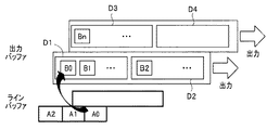
図4のラインバッファは図2のラインバッファ11に相当する。ラインバッファ11には、ラスタスキャン順で画素A0,A1,A2…が順次書き込まれる。ラインバッファ11に書き込まれた画素は歪補正回路1によって補正画素位置が決定される。図4の出力バッファは所定の伝送単位(例えば64バイト)毎の複数の領域D1,D2,…(以下、これらを区別する必要がない場合には領域Dという)を有する。DRAM24への転送は各伝送単位毎に行われる。従って、出力バッファの各領域D内の全アドレスに、ラスタスキャン順の画素値が格納される毎に各領域Dから画素値が出力されてDRAM24に転送されることになる。なお、出力バッファの各領域Dは、最初に書き込まれる画素の補正画素位置に応じたアドレスが付与され、各領域Dに格納された画素は、DRAM24の対応するアドレスに書き込まれる。
The line buffer of FIG. 4 corresponds to the
例えば画素A0,A1の補正画素位置が連続している場合において、画素A0が出力バッファの領域D1の先頭位置に画素B0として書き込まれた場合には、次の画素A1に対応する画素B1は画素B0が格納された次のアドレスの位置に書き込まれる。しかし、画素A2の補正画素位置が画素A1の補正画素位置に対して領域D1に格納できる画素数分の画素位置よりも離間している場合には、画素A2に対応する画素B2は領域D1以外の他の領域に書き込まれる。図4の例では画素A2に対応した画素B2は、出力バッファの領域D2に格納されている。なお、領域D3には画素Anに対応した画素Bnが格納されていることを示している。 For example, when the correction pixel positions of the pixels A0 and A1 are continuous and the pixel A0 is written as the pixel B0 at the head position of the output buffer area D1, the pixel B1 corresponding to the next pixel A1 is a pixel. It is written to the position of the next address where B0 is stored. However, when the correction pixel position of the pixel A2 is separated from the correction pixel position of the pixel A1 by the number of pixels that can be stored in the area D1, the pixel B2 corresponding to the pixel A2 is other than the area D1. Written to other areas. In the example of FIG. 4, the pixel B2 corresponding to the pixel A2 is stored in the output buffer area D2. It is shown that the pixel Bn corresponding to the pixel An is stored in the area D3.
このように、ラスタスキャン入力・ランダム出力の歪補正処理を行った場合には、出力バッファの連続したアドレスに順次画素が書き込まれるとは限らないので、出力バッファの利用効率が低下する。出力バッファの利用効率を向上させるために伝送単位の出力バッファサイズを小さくすると、DRAM転送の占有率が大きくなって伝送効率が低下する。例えば、64バイトサイズの出力バッファを採用した場合には、伝送効率は、ラスタスキャン入力・ラスタスキャン出力時の30%程度に低下する。このため、画像処理回路21によるDRAM転送の占有率が大きくなり、画像解析等の他の処理に長時間を要してしまう。逆に、伝送効率を向上させようとすると、結果的にトータルの出力バッファサイズが増大してしまう。
In this way, when the distortion correction processing of the raster scan input / random output is performed, the pixels are not always written sequentially to the continuous addresses of the output buffer, so that the utilization efficiency of the output buffer is lowered. If the output buffer size of the transmission unit is reduced in order to improve the utilization efficiency of the output buffer, the occupancy rate of the DRAM transfer increases and the transmission efficiency decreases. For example, when a 64-byte size output buffer is adopted, the transmission efficiency is reduced to about 30% of that at the time of raster scan input / raster scan output. Therefore, the occupancy rate of the DRAM transfer by the
そこで、本実施の形態においては、レンズ歪みの特性に応じて、出力バッファを多層化することで、出力バッファ全体の利用効率を向上させる。これにより、出力バッファサイズの低減及びDRAM転送の伝送効率の向上を図る。 Therefore, in the present embodiment, the utilization efficiency of the entire output buffer is improved by forming the output buffer in multiple layers according to the characteristics of the lens distortion. As a result, the output buffer size is reduced and the transmission efficiency of DRAM transfer is improved.
図5は図1中のバッファ回路3の具体的な構成の一例を示すブロック図である。図5の例は出力バッファを2段に多層化した例を示しているが、3段以上に多層化してもよい。
FIG. 5 is a block diagram showing an example of a specific configuration of the
図5においてバッファ回路3はコントローラ31と、出力バッファ32,33を備えている。出力バッファ32は1段目の出力バッファであり、出力バッファ33は2段目の出力バッファである。コントローラ31は出力バッファ32,33の書き込み及び読み出しを制御する。
In FIG. 5, the
出力バッファ32は、所定の容量の複数の領域E1を有しており、出力バッファ33は、所定の容量の複数の領域E2を有している。領域E1,E2の容量は独立して設定可能である。例えば、領域E1の容量と領域E2の容量との和の容量を伝送単位の容量に設定する。
The
例えば、領域E1,E2の容量がいずれも64バイトであるものとすると、1画素が16ビットデータの場合には各領域E1,E2にそれぞれ32画素が格納可能であり、1画素が8ビットデータの場合には各領域E1,E2にそれぞれ64画素が格納可能である。以下、領域E1又はE2にそれぞれ格納される補正画素位置が連続する一連の画素の集合をそれぞれサブブロックというものとし、2つの領域E1及びE2に格納された補正画素位置が連続した伝送単位の一連の画素の集合を伝送ブロックというものとする。なお、出力バッファが3段以上で構成される場合には、これらの3段以上の出力バッファに格納されている補正画素位置が連続した伝送単位の一連の画素の集合を伝送ブロックという。 For example, assuming that the capacities of the areas E1 and E2 are 64 bytes, if one pixel is 16-bit data, 32 pixels can be stored in each of the areas E1 and E2, and one pixel is 8-bit data. In the case of, 64 pixels can be stored in each of the areas E1 and E2. Hereinafter, a set of a series of pixels in which the correction pixel positions stored in the regions E1 or E2 are continuous is referred to as a subblock, respectively, and a series of transmission units in which the correction pixel positions stored in the two regions E1 and E2 are continuous. The set of pixels of is called a transmission block. When the output buffer is composed of three or more stages, a set of a series of pixels of a transmission unit in which the correction pixel positions stored in these three or more stages of output buffers are continuous is called a transmission block.
コントローラ31は、ポスト処理回路2からランダムな順に出力される各画素を先ず出力バッファ32の複数の領域E1のうちのいずれかの領域E1に与える。出力バッファ32の各領域E1には、最初に書き込まれる画素の補正画素位置に応じたタグ情報が付与される。コントローラ31は、補正画素位置が連続する画素は各領域E1の連続したアドレスに書き込む。つまり、領域E1の容量が64バイトで、1画素が16ビットデータの場合には、各領域E1に補正画素位置が連続する32画素分の画素が格納される。例えば、伝送単位である伝送ブロックが64画素で構成される場合には、領域E1には伝送ブロックの半分の画素のサブブロックが格納可能である。コントローラ31は、出力バッファ32の各領域E1毎に領域内の全アドレスに画素が格納された状態になったか否かを判定する。以下、各領域E1毎にサブブロックの全データが格納されたことを充填完了とも言い、コントローラ31は、充填完了となった領域E1毎に格納されているサブブロックの画素を後段の出力バッファ33に転送する。
The
出力バッファ33の各領域E2にも、最初に書き込まれる画素の補正画素位置に応じたタグ情報が付与される。コントローラ31は、補正画素位置が連続する画素は各領域E2の連続したアドレスに書き込む。つまり、例えば、領域E2の容量が64バイトで、1画素が16ビットデータの場合には、各領域E2に補正画素位置が連続する32画素分の画素が格納される。1伝送ブロックが64画素で構成される場合には、領域E1,E2に格納されたサブブロックを連結することで、伝送ブロックの画素が得られる。コントローラ31は、出力バッファ33の各領域E2毎に充填完了になったか否かを判定する。コントローラ31は、領域E2が充填完了となった場合において、当該領域E2に格納された画素と、この画素に補正画素位置が連続する画素を格納する領域E1に格納された画素とで、伝送ブロックの全データが格納される(以下、この場合も充填完了という)状態になると、これらの領域E1,E2に格納されている全画素、即ち、補正画素位置が連続する伝送単位の複数の画素(伝送ブロックの全画素)をバス23を介してDRAM24に転送して記憶させるようになっている。
Tag information corresponding to the correction pixel position of the pixel to be written first is also added to each area E2 of the
次に、図6及び図7を参照して本実施の形態における多層化された出力バッファ32,33によって出力バッファの利用効率を向上させることができる理由について説明する。図6は多層化されていない場合の出力バッファの書き込み及び読み出しを示し、図7は多層化されている場合の出力バッファの書き込み及び読み出しを示している。 Next, the reason why the utilization efficiency of the output buffer can be improved by the multi-layered output buffers 32 and 33 in the present embodiment will be described with reference to FIGS. 6 and 7. FIG. 6 shows the writing and reading of the output buffer when the layers are not multi-layered, and FIG. 7 shows the writing and reading of the output buffer when the layers are not multi-layered.
図6及び図7は説明を簡略化するために、撮像部22からの撮像画像が水平方向に16画素であるものとし、DRAM24への伝送単位が4画素であるものとして説明する。図6及び図7の例は撮像部22の光学系の収差等の影響により破線にて示すたる型歪が生じた結果、本来画像の第1ラインの各画素が図6及び図7の画素a1〜a4,b1〜b4,c1〜c4,d1〜d4の位置に移動した画像として歪補正回路1に入力されたことを示している。撮像部22からの各画素はラスタスキャン順で歪補正回路1に入力され、入力された画素順で画像処理が行われて出力バッファに与えられる。
In FIG. 6 and FIG. 7, for simplification of the description, it is assumed that the image captured from the
図6の例は出力バッファが階層化されておらず伝送単位である4画素分の3つの領域D1〜D3を有している例を示している。図6の例では、画素a1〜a4,b1〜b4,c1〜c4,d1〜d4のうち歪補正回路1に最初に入力される画素は画素d1である。この画素d1は出力バッファの例えば領域D3に格納される。第2ラインの左から3番目の画素a3及び画素a4が順次歪補正回路1に入力されて処理されると、処理後の画素a3,a4は領域D1の連続する位置に書き込まれる。次に、補正画素位置が連続する画素b1〜b4が順次入力され、これらの補正画素位置が連続する画素b1〜b4は、領域D2に順次格納される。領域D2が充填完了すると、領域D2に格納されている全ての画素が読み出されてDRAMに転送される。
The example of FIG. 6 shows an example in which the output buffer is not layered and has three regions D1 to D3 for four pixels, which are transmission units. In the example of FIG. 6, among the pixels a1 to a4, b1 to b4, c1 to c4, and d1 to d4, the pixel first input to the
図6の太枠の画素まで処理が進んだ状態では、領域D2は充填完了後に転送されて空き状態となる一方、領域D1は第3ラインの左から1番目及び2番目の画素a1,a2の処理が行われるまで充填状態とはならず、また、領域D3は第3ラインの右から2番目の画素d4の処理が行われるまで充填状態とはならない。即ち、出力バッファに空きがあるにも拘わらず、これらの空き領域は利用されず、利用効率が低い状態である。 In the state where the processing has progressed to the pixels in the thick frame of FIG. 6, the area D2 is transferred after the filling is completed and becomes an empty state, while the area D1 is the first and second pixels a1 and a2 from the left of the third line. The region D3 is not in the filled state until the processing is performed, and the region D3 is not in the filled state until the processing of the second pixel d4 from the right of the third line is performed. That is, although there is space in the output buffer, these free areas are not used and the utilization efficiency is low.
図7の例は出力バッファを2段に多層化した例を示しており、出力バッファ32に相当する領域E1a,E1bにより1段目出力バッファを構成し、出力バッファ33に相当する領域E2a,E2bにより2段目出力バッファを構成した例を示している。領域E1a,E1b,E2a,E2bはいずれも2画素分の容量を有している。
The example of FIG. 7 shows an example in which the output buffer is multi-layered in two stages. The first stage output buffer is configured by the areas E1a and E1b corresponding to the
画素a1〜a4,b1〜b4,c1〜c4,d1〜d4のうち歪補正回路1に最初に入力される画素d1は、1段目出力バッファの例えば領域E1bに格納される。第2ラインの左から3番目の画素a3及び画素a4が順次歪補正回路1に入力されて処理されると、処理後の画素a3,a4は領域E1aの位置に書き込まれる。コントローラ31は領域E1aが充填完了すると、領域E1aに格納されているサブブロックの画素a3,a4を2段目出力バッファの例えば領域E2aに転送して記憶させ、領域E1aを空き状態とする。
Of the pixels a1 to a4, b1 to b4, c1 to c4, and d1 to d4, the pixel d1 first input to the
次に、補正画素位置が連続する画素b1〜b4が順次入力される。先ず、画素b1,b2は、領域E1aに書き込まれ、更にコントローラ31によって領域E2bに転送される。更に、コントローラ31は、空き領域E1aに画素b3,b4を書き込む。コントローラ31は、2段目出力バッファを構成する領域E2bが充填完了すると共に、この領域E2bに格納されている画素に補正画素位置が連続する画素によって、1段目出力バッファの領域が充填完了すると、これらの2つの領域の画素、即ち、領域E2b,E1aに格納されている伝送ブロックの全ての画素をバス23を介してDRAM24に転送する。これにより、これらの領域E1a,E2bは空き領域となる。
Next, pixels b1 to b4 having continuous correction pixel positions are sequentially input. First, the pixels b1 and b2 are written in the area E1a and further transferred to the area E2b by the
即ち、図7の太枠に示す画素まで処理が進んでいる状態では、1段目出力バッファE1aは空き領域となっており、次に歪補正処理が終了した画素の書き込みが可能となる。即ち、図7の例は図6の例に比べて出力バッファの利用効率が向上している。この結果、図7の例では、図6の合計出力バッファサイズ(4×3=12画素分)よりも少ない合計出力バッファサイズ(2×4=8画素分)でバッファ回路を構成可能である。 That is, in a state where the processing has progressed to the pixels shown in the thick frame of FIG. 7, the first-stage output buffer E1a is an empty area, and then the pixels for which the distortion correction processing has been completed can be written. That is, in the example of FIG. 7, the utilization efficiency of the output buffer is improved as compared with the example of FIG. As a result, in the example of FIG. 7, the buffer circuit can be configured with a total output buffer size (2 × 4 = 8 pixels) smaller than the total output buffer size (4 × 3 = 12 pixels) of FIG.
図6及び図7に示すたる型歪では、画像中央ほど歪が小さく、画像の四隅程歪が大きい。このため、画像中央近傍では、各画素は歪補正回路1への入力順と略同じ順で出力され、1段目バッファの各領域E1は充填速度が比較的高く、比較的短時間で充填完了する。逆に、画像四隅近傍では、各画素の歪補正回路1への入力順と出力順とは比較的大きく異なり、1段目バッファの各領域E1は充填速度が比較的遅く、充填完了するまでに比較的長時間を要する。
In the barrel distortion shown in FIGS. 6 and 7, the distortion is smaller toward the center of the image and larger at the four corners of the image. Therefore, in the vicinity of the center of the image, each pixel is output in substantially the same order as the input to the
仮に、歪がない場合又は画像全体で一様な歪の場合には、出力バッファを多層化しても効果はない。しかし、たる型歪等のように画像の位置に応じて不均一な歪が生じている場合には、画素位置によってバッファ充填速度が不均一となる。このため、1段目バッファのバッファサイズを比較的小さくすることで、充填速度の速い画素位置の画素によるバッファ利用効率を高めると共に、充填速度の遅い画素位置の画素によるバッファ利用効率の低下を抑制することができる。これにより、合計バッファサイズを低減化し伝送効率を向上させることが可能である。なお、経験則によれば、1段目の出力バッファ32の領域E1の数≧2段目の出力バッファ33の領域E2の数として構成した方がよい。3段以上で出力バッファを階層化する場合には、1段目の出力バッファ数≧2段目の出力バッファ数≧3段目の出力バッファ数≧・・・とする。
If there is no distortion or the distortion is uniform over the entire image, there is no effect even if the output buffer is multi-layered. However, when non-uniform distortion occurs depending on the position of the image such as barrel distortion, the buffer filling speed becomes non-uniform depending on the pixel position. Therefore, by making the buffer size of the first stage buffer relatively small, the buffer utilization efficiency of the pixels at the pixel positions having a high filling speed is increased, and the decrease in the buffer utilization efficiency due to the pixels at the pixel positions with a slow filling speed is suppressed. can do. This makes it possible to reduce the total buffer size and improve the transmission efficiency. According to an empirical rule, it is preferable to configure the number of regions E1 of the first-
図8A及び図8Bはバッファ回路3の動作を更に詳細に説明するための説明図である。図8Aは出力バッファ32の動作を示すためのものであり、図8Bは出力バッファ33の動作を示すためのものである。
8A and 8B are explanatory views for explaining the operation of the
図8Aは出力バッファ32を示しており、サブブロックの画素を記憶する[0],[1],…[i]にて示す複数の領域E1(以下、これらの領域を区別する必要がある場合には領域E1[0],E1[1],…E1[i]という)がそれぞれNバイトの容量を有すると共に、各領域E1毎にタグ情報が付加されることを示している。即ち、図8Aの例では出力バッファ32は(i+1)個の領域E1を有している。なお、各領域E1には、画素が記憶されることによって、当該画素の画像位置に対応したタグ情報が付加されて記憶されるようになっている。
FIG. 8A shows the
領域E1,E2には補正画素位置が連続した一連の画素(サブブロックの画素)が記憶されることから、1つの領域E1,E2に1つのタグ情報を付加することで、各領域E1,E2に記憶されたサブブロックの画素位置を特定することが可能であり、領域E1,E2の各画素の記憶領域毎にアドレスを付加する必要はない。 Since a series of pixels (subblock pixels) in which the correction pixel positions are continuous are stored in the areas E1 and E2, by adding one tag information to one area E1 and E2, each area E1 and E2 It is possible to specify the pixel position of the subblock stored in the above, and it is not necessary to add an address to each storage area of each pixel of the areas E1 and E2.
図8Bは出力バッファ33を示しており、サブブロックの画素を記憶する[0],[1],…[j]にて示す複数の領域E2(以下、これらの領域を区別する必要がある場合には領域E2[0],E2[1],…E2[j]という)がそれぞれNバイトの容量を有することを示している。即ち、図8Bの例では出力バッファ33は(j+1)個の領域E2を有している。出力バッファ33においても、各領域E2毎にタグ情報が付加される。なお、各領域E2には、出力バッファ32から画素が転送されることによって、転送されたサブブロックに対応して付加されたタグ情報が記憶されるようになっている。
FIG. 8B shows the
コントローラ31は、出力バッファ32から出力バッファ33への画素の転送をタグ情報により管理する。これにより、コントローラ31は、2つのサブブロックである領域E1,E2に格納された補正画素位置が連続する伝送ブロックの一連の画素を、画像位置を示すタグ情報を付加して出力することができる。バッファ回路3の出力はバス23を介してDRAM24に与えられて記憶される。
The
図8A及び図8Bの例では、伝送ブロックを構成する補正画素位置が連続する一連の画素a1,a2,…,an,an+1,…,amのうち、先ず画素a1,a2,…,anが出力バッファ32の所定の領域E1に記憶されるものとする。この場合には、画素a1,a2,…,anの画像位置に対応したタグ情報tag02が付加されて当該領域E1に記憶される。コントローラ31は、領域E1が充填完了すると、これらのサブブロックの画素a1,a2,…,anを出力バッファ33の領域E2、例えば領域E2[1]に転送して記憶させる。
In the examples of FIGS. 8A and 8B, among a series of pixels a1, a2 ..., an, an + 1, ..., Am in which the correction pixel positions constituting the transmission block are continuous, the pixels a1, a2, ..., An are output first. It is assumed that it is stored in the predetermined area E1 of the
次に、画素a1,a2,…,anに補正画素位置が連続する画素an+1,…,amが出力バッファ32の領域E1、例えば、領域E1[0]に書き込まれるものとする。この場合には、領域E1[0]には、領域E2[1]のタグ情報tag02に画像位置が連続することを示すタグ情報tag01が付加されて記憶される。画素an+1,…,amにより領域E1[0]が充填完了すると、コントローラ31は、タグ情報を利用して、出力バッファ33の領域E2[1]と出力バッファ32の領域E1[0]とに格納されている伝送ブロックの画素、即ち、補正画素位置が連続する一連の画素a1,a2,…,an,an+1,…,amを読み出し、バス23を介してDRAM24に転送する。この場合には、コントローラ31は、画素a1,a2,…,an,an+1,…,amの画像位置に対応するタグ情報tag0を付加する。
Next, it is assumed that the pixels an + 1, ..., Am whose correction pixel positions are continuous with the pixels a1, a2, ..., An are written in the area E1 of the
なお、図8A及び図8Bは、領域E1,E2に格納するサブブロックのサイズ(容量)はいずれもNバイト(n個の画素)の例を示しており、伝送ブロックサイズM=2Nであり、m=2nである。しかし、領域E2に格納したNバイト(n画素)のサブブロックと、領域E1に格納したNバイトよりも小さいサブブロックによって構成される伝送ブロックの画素を伝送することも可能であり、この場合には、M≧Nとなる。 Note that FIGS. 8A and 8B show an example in which the size (capacity) of the subblocks stored in the areas E1 and E2 is N bytes (n pixels), and the transmission block size M = 2N. m = 2n. However, it is also possible to transmit the pixels of the transmission block composed of the N-byte (n-pixel) subblock stored in the area E2 and the sub-block smaller than the N-byte stored in the area E1. In this case, Is M ≧ N.
また、領域E1,E2の数に対応するi,jは、i≧jとする。 Further, i and j corresponding to the numbers of the regions E1 and E2 are set to i ≧ j.
なお、図8A及び図8Bを用いた説明では、2段目の出力バッファ33には転送されたサブブロックに対応して付加されたタグ情報が記憶されるものと説明したが、この出力バッファ33に記憶されたサブブロックとこれに対応する1段目の出力バッファ32に記憶されたサブブロックとの画像上の位置関係が明確である場合には、出力バッファ33には伝送ブロックに対応した画像位置を示すタグ情報を記憶させるようになっていてもよい。
(評価)
撮像部22の光学系として所定の魚眼レンズを採用した場合において、歪補正に必要な出力バッファの容量について評価を行った。
In the description using FIGS. 8A and 8B, it was explained that the tag information added corresponding to the transferred subblock is stored in the
(Evaluation)
When a predetermined fisheye lens was adopted as the optical system of the
バス23を介してDRAM24への伝送単位である伝送ブロックサイズを128バイトに設定した場合についてシミュレーションを行い、図6のように出力バッファを1段で構成した場合と図7のように出力バッファを2段で構成した場合とについて、歪補正に必要な出力バッファ容量を求めた。なお、1画素は16ビットデータとし、1伝送ブロックは64画素の集合であるものとする。
A simulation was performed for the case where the transmission block size, which is the unit of transmission to the
シミュレーションによると、出力バッファを1段で構成した場合には、歪補正のために、1伝送ブロック(128バイト)を記憶する領域(以下、エントリともいう)を1001個有する出力バッファを用いる必要がある。即ち、この場合の出力バッファサイズは1001×128バイト=125Kバイトとなる。 According to the simulation, when the output buffer is configured in one stage, it is necessary to use an output buffer having 1001 areas (hereinafter, also referred to as entries) for storing one transmission block (128 bytes) for distortion correction. is there. That is, the output buffer size in this case is 1001 × 128 bytes = 125 Kbytes.
これに対し、出力バッファを2段で構成した場合には、歪補正のために、1サブブロック(64バイト)を記憶する領域(エントリ)E1を447個有する出力バッファ32と、1サブブロック(64バイト)を記憶する領域(エントリ)E2を232個有する出力バッファ33とを用いればよい。この場合の出力バッファサイズは、447×64バイト+232×64バイト=42Kバイトとなる。
On the other hand, when the output buffer is composed of two stages, the
即ち、この例では、出力バッファを多層化することにより、出力バッファの合計サイズを約1/3に低減可能である。なお、出力バッファの合計サイズを変更しないものとすると、出力バッファを多層化することにより伝送ブロックサイズを大きくすることができることになり、伝送効率を向上させることができる。 That is, in this example, the total size of the output buffers can be reduced to about 1/3 by forming the output buffers in multiple layers. If the total size of the output buffers is not changed, the transmission block size can be increased by increasing the number of layers of the output buffers, and the transmission efficiency can be improved.
このように本実施の形態においては、歪の形状に基づいて、画像の位置によって、出力バッファの充填速度が異なることを利用して、出力バッファを複数段に多層化し、各段のバッファ数(エントリ数)及びバッファサイズを適正な値とすることで、バッファメモリ容量を低減し伝送効率を向上させることが可能である。
(実装例)
図9は上述した(評価)の欄に対応したバッファ回路3の実装例を示す説明図である。図9の例は伝送ブロックサイズが128バイトであり、出力バッファ32の領域E1に相当する1段目バッファのエントリのサイズは64バイト、出力バッファ33の領域E2に相当する2段目バッファのエントリのサイズは64バイトである。(評価)の欄の記載に対応させて、1段目バッファのバッファ数(エントリ数)は最大で448エントリとし、2段目バッファのバッファ数(エントリ数)は最大で240エントリとする。なお、図9では各段毎に枠で囲った1エントリのみを示している。図9に示す書き込み及び読み出し制御は、コントローラ31によって実現される。
As described above, in the present embodiment, the output buffer is multi-layered in a plurality of stages by utilizing the fact that the filling speed of the output buffer differs depending on the position of the image based on the shape of the distortion, and the number of buffers in each stage ( By setting the number of entries) and the buffer size to appropriate values, it is possible to reduce the buffer memory capacity and improve the transmission efficiency.
(Implementation example)
FIG. 9 is an explanatory diagram showing an implementation example of the
また、YUV422プレーナーフォーマットを採用した場合には、UV画素(br)の出力データ幅はY画素(g)の半分の32バイトになる。そこで、図9ではUV画素用に2段目バッファ及び3段目バッファを用意し、2段目バッファによって32バイトのサブブロックを2連続した64バイトのサブブロックを作成し、3段目バッファによって、64バイトのサブブロックを2連続した128バイトの伝送ブロックを生成するようになっている。なお、これらのUV画素用の2段目及び3段目バッファのエントリ数はいずれも最大で240である。 Further, when the YUV422 planar format is adopted, the output data width of the UV pixel (br) is 32 bytes, which is half of the Y pixel (g). Therefore, in FIG. 9, a second-stage buffer and a third-stage buffer are prepared for UV pixels, a 32-byte subblock is created by the second-stage buffer to create a 64-byte subblock in which two consecutive 32-byte subblocks are created, and the third-stage buffer is used. , A 128-byte transmission block in which two 64-byte subblocks are consecutive is generated. The maximum number of entries in the second-stage and third-stage buffers for these UV pixels is 240.
また、図9では1画素は16ビットデータの例を示しているが、1段目バッファについては、参考のために、1画素が8ビットデータの場合についても例示してある。なお、図9では、[y:x]の表記によって、下位側の第xビットから上位側の第yビットのビット範囲のデータであることを示す。 Further, in FIG. 9, one pixel shows an example of 16-bit data, but for reference, the case where one pixel is 8-bit data is also illustrated for the first stage buffer. In FIG. 9, the notation of [y: x] indicates that the data is in the bit range from the lower xth bit to the upper yth bit.
バッファ回路3への入力画素は、水平方向の補正画素位置を示す13ビットの水平アドレスi_h[12:0]及び垂直方向の12ビットの垂直アドレスi_v[11:0]を有する。なお、入力画素は、G,B,Rの成分i_g_pix[15:0],i_b_pix[15:0],i_r_pix[15:0]の各16ビットのデータである。1画素は16ビットデータであるので、64バイトの1段目バッファの各エントリには、補正画素位置が連続する32画素分のサブブロックデータが格納される。
The input pixel to the
1段目バッファの1エントリに格納されたサブブロック毎に画像位置を特定するためのタグ情報を付加する。即ち、サブブロックを構成する入力画素32個分で1つのタグ情報を設定すればよく、入力画素の32個を表す水平アドレスの下位5ビットを除く上位8ビット、即ち、i_h[12:5]を水平方向のタグ情報とする。なお、各バッファにおいて、タグ情報の記憶に必要な容量を減少させるために、タグ情報として用いる垂直アドレスは、入力画素の下位6ビットのi_v[5:0]とする。なお、この場合には、連続する64バイト内で、垂直アドレスが64以上離れた歪みには対応することはできない。 Tag information for specifying the image position is added to each subblock stored in one entry of the first-stage buffer. That is, one tag information may be set for 32 input pixels constituting the subblock, and the upper 8 bits excluding the lower 5 bits of the horizontal address representing 32 input pixels, that is, i_h [12: 5]. Is the tag information in the horizontal direction. In each buffer, the vertical address used as the tag information is i_v [5: 0] of the lower 6 bits of the input pixel in order to reduce the capacity required for storing the tag information. In this case, it is not possible to deal with the distortion in which the vertical addresses are separated by 64 or more within the continuous 64 bytes.
また、1画素が8ビットデータの場合には、64バイトの1段目バッファの各エントリには、補正画素位置が連続する64画素分のサブブロックデータが格納される。この場合には、サブブロックを構成する入力画素64個分で1つのタグ情報を設定すればよく、入力画素の64個を表す水平アドレスの下位6ビットを除く上位7ビット、即ち、i_h[12:6]を水平方向のタグ情報とする。なお、垂直方向のタグ情報は入力画素の下位6ビットのi_v[5:0]とする。 When one pixel is 8-bit data, subblock data for 64 pixels having continuous correction pixel positions is stored in each entry of the 64-byte first-stage buffer. In this case, one tag information may be set for 64 input pixels constituting the subblock, and the upper 7 bits excluding the lower 6 bits of the horizontal address representing 64 input pixels, that is, i_h [12 : 6] is used as the tag information in the horizontal direction. The tag information in the vertical direction is i_v [5: 0] of the lower 6 bits of the input pixel.
1段目バッファの各エントリにサブブロックが充填完了すると、64バイトのgのサブブロックは2段目バッファに転送されて記憶される。更に、1段目バッファのいずれかのエントリに、2段目バッファに記憶されているサブブロックと共に伝送ブロックを構成するサブブロックが記憶されると、2段目バッファ及び1段目バッファに記憶されているサブブロックを連結した128バイトの伝送ブロックが出力される。この2段目バッファの出力には、画像位置に対応したタグ情報であるi_h[12:6],i_v[5:0]が付加される。 When each entry in the first-stage buffer is filled with subblocks, the 64-byte g subblock is transferred to the second-stage buffer and stored. Further, when the subblocks constituting the transmission block are stored together with the subblocks stored in the second stage buffer in any entry of the first stage buffer, they are stored in the second stage buffer and the first stage buffer. A 128-byte transmission block in which the sub-blocks are connected is output. Tag information i_h [12: 6] and i_v [5: 0] corresponding to the image position are added to the output of the second stage buffer.
なお、1段目バッファからは、サブブロックを構成する64バイト分がまとめて読み出される。しかし、サブブロックの読み出しを行う1段目バッファのエントリに連続的に書き込みデータが与えられる場合があり、この場合には、書き込み後に読み出しを行う余裕がない場合がある。そこで、コントローラ31は、サブブロックの最後のデータが1段目バッファの所定のエントリに入力されると、このデータの書き込み前にサブブロックのデータを読み出し、読み出したデータに入力された最後のデータを上書きして出力するようになっていてもよい。
From the first-stage buffer, 64 bytes constituting the sub-block are collectively read. However, write data may be continuously given to the entry of the first-stage buffer for reading the subblock, and in this case, there may be no room for reading after writing. Therefore, when the last data of the subblock is input to a predetermined entry of the first stage buffer, the
図10はこの動作を示す説明図である。図10は1画素が16ビットで、補正画素位置が連続した水平画素位置(0)〜(31)の32画素によってサブブロックが構成される例を示している。水平画素位置(10),(9),(11),…の順に1段目バッファの所定のエントリに画素が入力され、サブブロックを構成する最後の画素として水平画素位置(30)の画素(斜線部)が入力される。この水平画素位置(30)の画素が入力されると、当該画素の書き込み前に当該エントリからサブブロックのデータを読み出し、出力サブブロック中の斜線部に示すように、入力された水平画素位置(30)の画素のデータを対応するデータ位置に上書きして出力する。 FIG. 10 is an explanatory diagram showing this operation. FIG. 10 shows an example in which one pixel is 16 bits and a sub-block is composed of 32 pixels of horizontal pixel positions (0) to (31) in which correction pixel positions are continuous. Pixels are input to predetermined entries in the first-stage buffer in the order of horizontal pixel positions (10), (9), (11), ..., And pixels at the horizontal pixel position (30) are used as the last pixels constituting the subblock. The shaded area) is input. When a pixel at this horizontal pixel position (30) is input, the data of the subblock is read from the entry before writing the pixel, and as shown in the shaded area in the output subblock, the input horizontal pixel position ( The data of the pixel of 30) is overwritten on the corresponding data position and output.
なお、本発明は、上記実施形態に限定されるものではなく、実施段階ではその要旨を逸脱しない範囲で種々に変形することが可能である。また、上記実施形態には種々の段階の発明が含まれており、開示される複数の構成要件における適当な組み合わせにより種々の発明が抽出され得る。例えば、実施形態に示される全構成要件からいくつかの構成要件が削除されても、発明が解決しようとする課題の欄で述べた課題が解決でき、発明の効果の欄で述べられている効果が得られる場合には、この構成要件が削除された構成が発明として抽出され得る。 The present invention is not limited to the above embodiment, and can be variously modified at the implementation stage without departing from the gist thereof. In addition, the above-described embodiment includes inventions at various stages, and various inventions can be extracted by an appropriate combination in a plurality of disclosed constituent requirements. For example, even if some constituent requirements are deleted from all the constituent requirements shown in the embodiment, the problem described in the column of the problem to be solved by the invention can be solved, and the effect described in the column of effect of the invention can be solved. If is obtained, a configuration in which this configuration requirement is deleted can be extracted as an invention.
1…歪補正回路、2…ポスト処理回路、3…バッファ回路、11…ラインバッファ、21…画像処理回路、22…撮像部、23…バス、24…DRAM、25…CPU、31…コントローラ、32…出力バッファ、33…出力バッファ。 1 ... distortion correction circuit, 2 ... post processing circuit, 3 ... buffer circuit, 11 ... line buffer, 21 ... image processing circuit, 22 ... imaging unit, 23 ... bus, 24 ... DRAM, 25 ... CPU, 31 ... controller, 32. ... output buffer, 33 ... output buffer.
Claims (7)
前記歪補正回路の出力が前記補正画素位置の情報に基づくランダム順に入力される出力バッファであって、前記補正画素位置が連続する補正画素の集合である伝送ブロック毎に補正画素を出力する2段以上に階層化された複数の出力バッファと、
前記歪補正回路の出力画素を、前記複数の出力バッファのうち初段の出力バッファに書き込むと共に、書き込んだ画素を後段の出力バッファに順次転送するものであって、各段の出力バッファに前記伝送ブロックを分割したサブブロックを記憶させるコントローラとを具備した画像処理装置。 A plurality of pixels constituting the input image is input to the raster scan order, on the basis of the distortion of the input image be those obtaining the position correction pixel I line correction operation for correcting the said pixel, the pixel that is the input The first calculation for obtaining the correction pixel position, which is the position of the pixel to be output from the input pixel position, which is the position of, and the second calculation for obtaining the pixel position of the input image corresponding to the correction pixel position and the pixel positions of a plurality of pixels around the correction pixel position. 2 arithmetic, performs the correction operation comprising a third operation for obtaining said corrected pixel corresponding to the pixel positions of the input image, the information of the corrected pixel position obtained as a result of the first operation on the corrected pixel In addition, a distortion correction circuit that outputs the correction pixel to which the information of the correction pixel position is added, and
A two-stage output buffer in which the output of the distortion correction circuit is input in random order based on the correction pixel position information, and correction pixels are output for each transmission block which is a set of correction pixels in which the correction pixel positions are continuous. Multiple output buffers layered above and
The output pixels of the distortion correction circuit are written to the output buffer of the first stage among the plurality of output buffers, and the written pixels are sequentially transferred to the output buffer of the subsequent stage, and the transmission block is transferred to the output buffer of each stage. An image processing device including a controller for storing sub-blocks divided into.
前記第1の演算の結果得られた補正画素位置の情報を前記補正画素に付加して、前記補正画素位置の情報が付加された前記補正画素を出力し、
前記歪補正回路から前記補正画素位置の情報に基づくランダム順に入力された補正画素を、2段以上に階層化された複数の出力バッファのうち初段の出力バッファに書き込むと共に、書き込んだ補正画素を後段の出力バッファに順次転送することで、各段の出力バッファに前記補正画素位置が連続する補正画素の集合であるサブブロックの画素を記憶させ、前記各段の出力バッファに記憶された複数のサブブロックを連結した伝送ブロックの画素を出力する画像処理方法。 The distortion correction circuit is a correction calculation in which a plurality of pixels constituting the input image are input in the order of raster scan and the position of the pixel is corrected based on the distortion of the input image, which is the position of the input pixel. The first calculation for obtaining the correction pixel position, which is the position of the pixel to be output from the input pixel position, and the second calculation for obtaining the pixel position of the input image corresponding to the correction pixel position and the pixel positions of a plurality of pixels around the correction pixel position. And the correction calculation including the third calculation for obtaining the correction pixel corresponding to the pixel position of the input image is performed.
The information of the correction pixel position obtained as a result of the first calculation is added to the correction pixel, and the correction pixel to which the information of the correction pixel position is added is output.
The correction pixels input from the distortion correction circuit in a random order based on the correction pixel position information are written to the output buffer of the first stage among a plurality of output buffers layered in two or more stages, and the written correction pixels are written to the latter stage. by sequentially transferred to the output buffer, to store the pixel sub-block is a set of corrected pixel where the corrected pixel position in the output buffer of each stage is continuous, the plurality of sub-stored in the output buffer of each stage An image processing method that outputs the pixels of a transmission block in which blocks are connected.
Priority Applications (5)
| Application Number | Priority Date | Filing Date | Title |
|---|---|---|---|
| JP2018048345A JP6845173B2 (en) | 2018-03-15 | 2018-03-15 | Image processing device and image processing method |
| KR1020180094839A KR102128534B1 (en) | 2018-03-15 | 2018-08-14 | Image processing device and image processing method |
| CN201810939611.0A CN110278394B (en) | 2018-03-15 | 2018-08-17 | Image processing apparatus and image processing method |
| EP18192181.8A EP3540684B1 (en) | 2018-03-15 | 2018-09-03 | Image processing apparatus and image processing method |
| US16/122,378 US10652487B2 (en) | 2018-03-15 | 2018-09-05 | Image processing apparatus and image processing method |
Applications Claiming Priority (1)
| Application Number | Priority Date | Filing Date | Title |
|---|---|---|---|
| JP2018048345A JP6845173B2 (en) | 2018-03-15 | 2018-03-15 | Image processing device and image processing method |
Publications (3)
| Publication Number | Publication Date |
|---|---|
| JP2019160063A JP2019160063A (en) | 2019-09-19 |
| JP2019160063A5 JP2019160063A5 (en) | 2020-03-12 |
| JP6845173B2 true JP6845173B2 (en) | 2021-03-17 |
Family
ID=63667678
Family Applications (1)
| Application Number | Title | Priority Date | Filing Date |
|---|---|---|---|
| JP2018048345A Active JP6845173B2 (en) | 2018-03-15 | 2018-03-15 | Image processing device and image processing method |
Country Status (5)
| Country | Link |
|---|---|
| US (1) | US10652487B2 (en) |
| EP (1) | EP3540684B1 (en) |
| JP (1) | JP6845173B2 (en) |
| KR (1) | KR102128534B1 (en) |
| CN (1) | CN110278394B (en) |
Families Citing this family (6)
| Publication number | Priority date | Publication date | Assignee | Title |
|---|---|---|---|---|
| JP7170478B2 (en) | 2018-09-18 | 2022-11-14 | 株式会社東芝 | Image processing device, image processing method and image processing program |
| JP7278750B2 (en) * | 2018-11-14 | 2023-05-22 | キヤノン株式会社 | Imaging device |
| JP7210337B2 (en) | 2019-03-14 | 2023-01-23 | 株式会社東芝 | Image processing device and distortion correction coefficient calculation method |
| JP7404201B2 (en) | 2020-09-11 | 2023-12-25 | 株式会社東芝 | Image processing device and image processing method |
| JP7419204B2 (en) | 2020-09-18 | 2024-01-22 | 株式会社東芝 | Image processing device |
| CN113630565B (en) * | 2021-07-09 | 2023-04-11 | 中国科学院西安光学精密机械研究所 | SCMOS imaging circuit with built-in real-time image processing function and method |
Family Cites Families (20)
| Publication number | Priority date | Publication date | Assignee | Title |
|---|---|---|---|---|
| JPS562532B2 (en) | 1973-10-26 | 1981-01-20 | ||
| US6924816B2 (en) * | 2000-03-17 | 2005-08-02 | Sun Microsystems, Inc. | Compensating for the chromatic distortion of displayed images |
| JP2005229200A (en) | 2004-02-10 | 2005-08-25 | Fujitsu Ltd | Distortion correcting circuit |
| JP4279775B2 (en) * | 2004-12-10 | 2009-06-17 | 富士フイルム株式会社 | Optical distortion correction apparatus, optical distortion correction method, and imaging apparatus |
| JP2007079708A (en) | 2005-09-12 | 2007-03-29 | Konica Minolta Holdings Inc | Image processor and processing method |
| US8503817B2 (en) * | 2006-03-01 | 2013-08-06 | Panasonic Corporation | Apparatus, method and imaging apparatus for correcting distortion of image data using interpolation |
| JP2007293457A (en) | 2006-04-21 | 2007-11-08 | Yamaha Corp | Image processor |
| US20090087115A1 (en) * | 2007-10-02 | 2009-04-02 | Ping Wah Wong | Correction for geometric distortion in images in pipelined hardware |
| JP4919978B2 (en) * | 2008-01-26 | 2012-04-18 | 三洋電機株式会社 | Distortion correction device |
| JP2010028758A (en) * | 2008-07-24 | 2010-02-04 | Sony Corp | Image processing apparatus and method, program, and imaging apparatus |
| US8369632B2 (en) * | 2009-04-08 | 2013-02-05 | Olympus Corporation | Image processing apparatus and imaging apparatus |
| JP5602532B2 (en) | 2010-07-30 | 2014-10-08 | オリンパス株式会社 | Image processing apparatus and image processing method |
| JP5719986B2 (en) * | 2010-10-20 | 2015-05-20 | パナソニックIpマネジメント株式会社 | Image processing apparatus and image processing method |
| US8952973B2 (en) * | 2012-07-11 | 2015-02-10 | Samsung Electronics Co., Ltd. | Image signal processor and method of operating the same |
| JP5947143B2 (en) | 2012-08-07 | 2016-07-06 | 株式会社日立情報通信エンジニアリング | Fisheye image correction apparatus and correction method |
| JP6136190B2 (en) * | 2012-10-23 | 2017-05-31 | 株式会社ソシオネクスト | Image processing apparatus and imaging apparatus |
| KR101520041B1 (en) * | 2013-09-10 | 2015-05-14 | 한국항공대학교산학협력단 | Device and method of an memory interface for lens distortion correction |
| TWI635746B (en) * | 2016-05-10 | 2018-09-11 | 晨星半導體股份有限公司 | Distorted image correcting apparatus and method |
| CN107437235A (en) * | 2016-05-27 | 2017-12-05 | 晨星半导体股份有限公司 | Distort Picture Calibration device and method |
| CN107249096B (en) * | 2016-06-14 | 2021-02-26 | 杭州海康威视数字技术股份有限公司 | Panoramic camera and shooting method thereof |
-
2018
- 2018-03-15 JP JP2018048345A patent/JP6845173B2/en active Active
- 2018-08-14 KR KR1020180094839A patent/KR102128534B1/en active IP Right Grant
- 2018-08-17 CN CN201810939611.0A patent/CN110278394B/en active Active
- 2018-09-03 EP EP18192181.8A patent/EP3540684B1/en active Active
- 2018-09-05 US US16/122,378 patent/US10652487B2/en active Active
Also Published As
| Publication number | Publication date |
|---|---|
| KR102128534B1 (en) | 2020-06-30 |
| US10652487B2 (en) | 2020-05-12 |
| EP3540684B1 (en) | 2022-03-09 |
| JP2019160063A (en) | 2019-09-19 |
| KR20190109196A (en) | 2019-09-25 |
| CN110278394A (en) | 2019-09-24 |
| US20190289231A1 (en) | 2019-09-19 |
| EP3540684A1 (en) | 2019-09-18 |
| CN110278394B (en) | 2021-12-10 |
Similar Documents
| Publication | Publication Date | Title |
|---|---|---|
| JP6845173B2 (en) | Image processing device and image processing method | |
| JP4657367B2 (en) | Image processing apparatus, imaging apparatus, and image distortion correction method | |
| JP4781229B2 (en) | Distortion correction apparatus, imaging apparatus, and control method for distortion correction apparatus | |
| US20100020225A1 (en) | Image processing apparatus, image processing method, and program | |
| JP5602532B2 (en) | Image processing apparatus and image processing method | |
| JP7170478B2 (en) | Image processing device, image processing method and image processing program | |
| JP4124096B2 (en) | Image processing method, image processing apparatus, and program | |
| JP2007267379A (en) | Image processing apparatus for correcting distortion of image, imaging apparatus, and method of correcting distortion of image | |
| JP2007184720A (en) | Image photographing apparatus | |
| JP5947143B2 (en) | Fisheye image correction apparatus and correction method | |
| JP2020149473A (en) | Image processing device and distortion correction coefficient calculation method | |
| US8509568B2 (en) | Image processing apparatus and image processing method | |
| JP7404201B2 (en) | Image processing device and image processing method | |
| WO2015098721A1 (en) | Image processing device, image processing method, image processing program, and imaging device | |
| JP6440465B2 (en) | Image processing apparatus, image processing method, and program | |
| JP2009003953A (en) | Image processor | |
| JP2010154035A (en) | Distortion correction device | |
| JP6273881B2 (en) | Image processing apparatus, image processing method, and program | |
| JP2016103169A (en) | Image processing apparatus, image processing method, and electronic apparatus | |
| JP2017017672A (en) | Image processing device, image processing method and image processing program | |
| JP5003739B2 (en) | Image display device and image display method | |
| JP2013187630A (en) | Picture processing device and method, and imaging device | |
| JP2016133957A (en) | Image processing apparatus, image processing method and image processing program | |
| JP2019125925A (en) | Image processing device and image formation device |
Legal Events
| Date | Code | Title | Description |
|---|---|---|---|
| RD01 | Notification of change of attorney |
Free format text: JAPANESE INTERMEDIATE CODE: A7421 Effective date: 20191008 |
|
| A521 | Request for written amendment filed |
Free format text: JAPANESE INTERMEDIATE CODE: A523 Effective date: 20200131 |
|
| A621 | Written request for application examination |
Free format text: JAPANESE INTERMEDIATE CODE: A621 Effective date: 20200131 |
|
| TRDD | Decision of grant or rejection written | ||
| A01 | Written decision to grant a patent or to grant a registration (utility model) |
Free format text: JAPANESE INTERMEDIATE CODE: A01 Effective date: 20210126 |
|
| A61 | First payment of annual fees (during grant procedure) |
Free format text: JAPANESE INTERMEDIATE CODE: A61 Effective date: 20210225 |
|
| R150 | Certificate of patent or registration of utility model |
Ref document number: 6845173 Country of ref document: JP Free format text: JAPANESE INTERMEDIATE CODE: R150 |