JP6804454B2 - High-speed mode transition in power converter - Google Patents
High-speed mode transition in power converter Download PDFInfo
- Publication number
- JP6804454B2 JP6804454B2 JP2017535449A JP2017535449A JP6804454B2 JP 6804454 B2 JP6804454 B2 JP 6804454B2 JP 2017535449 A JP2017535449 A JP 2017535449A JP 2017535449 A JP2017535449 A JP 2017535449A JP 6804454 B2 JP6804454 B2 JP 6804454B2
- Authority
- JP
- Japan
- Prior art keywords
- time period
- output stage
- mode
- power output
- pwm
- Prior art date
- Legal status (The legal status is an assumption and is not a legal conclusion. Google has not performed a legal analysis and makes no representation as to the accuracy of the status listed.)
- Active
Links
- 230000007704 transition Effects 0.000 title description 62
- 230000004044 response Effects 0.000 claims description 25
- 238000000034 method Methods 0.000 claims description 20
- 230000005540 biological transmission Effects 0.000 description 10
- 238000004891 communication Methods 0.000 description 8
- 238000010586 diagram Methods 0.000 description 8
- 230000033228 biological regulation Effects 0.000 description 7
- 238000004146 energy storage Methods 0.000 description 7
- 238000003860 storage Methods 0.000 description 6
- 239000003990 capacitor Substances 0.000 description 5
- 230000001105 regulatory effect Effects 0.000 description 5
- 238000004088 simulation Methods 0.000 description 4
- 238000002360 preparation method Methods 0.000 description 2
- 230000008569 process Effects 0.000 description 2
- 239000000758 substrate Substances 0.000 description 2
- 230000015572 biosynthetic process Effects 0.000 description 1
- 239000002131 composite material Substances 0.000 description 1
- 230000001276 controlling effect Effects 0.000 description 1
- 230000008878 coupling Effects 0.000 description 1
- 238000010168 coupling process Methods 0.000 description 1
- 238000005859 coupling reaction Methods 0.000 description 1
- 238000013461 design Methods 0.000 description 1
- 239000000446 fuel Substances 0.000 description 1
- 230000006870 function Effects 0.000 description 1
- 230000001939 inductive effect Effects 0.000 description 1
- 238000004519 manufacturing process Methods 0.000 description 1
- 230000000873 masking effect Effects 0.000 description 1
- 238000012986 modification Methods 0.000 description 1
- 230000004048 modification Effects 0.000 description 1
- 230000002093 peripheral effect Effects 0.000 description 1
- 238000010248 power generation Methods 0.000 description 1
- 238000012545 processing Methods 0.000 description 1
- 239000004065 semiconductor Substances 0.000 description 1
- 230000011664 signaling Effects 0.000 description 1
- 230000003595 spectral effect Effects 0.000 description 1
- 230000006641 stabilisation Effects 0.000 description 1
- 238000011105 stabilization Methods 0.000 description 1
- 230000000087 stabilizing effect Effects 0.000 description 1
- 238000012360 testing method Methods 0.000 description 1
Images


Classifications
-
- H—ELECTRICITY
- H02—GENERATION; CONVERSION OR DISTRIBUTION OF ELECTRIC POWER
- H02M—APPARATUS FOR CONVERSION BETWEEN AC AND AC, BETWEEN AC AND DC, OR BETWEEN DC AND DC, AND FOR USE WITH MAINS OR SIMILAR POWER SUPPLY SYSTEMS; CONVERSION OF DC OR AC INPUT POWER INTO SURGE OUTPUT POWER; CONTROL OR REGULATION THEREOF
- H02M3/00—Conversion of dc power input into dc power output
- H02M3/02—Conversion of dc power input into dc power output without intermediate conversion into ac
- H02M3/04—Conversion of dc power input into dc power output without intermediate conversion into ac by static converters
- H02M3/10—Conversion of dc power input into dc power output without intermediate conversion into ac by static converters using discharge tubes with control electrode or semiconductor devices with control electrode
- H02M3/145—Conversion of dc power input into dc power output without intermediate conversion into ac by static converters using discharge tubes with control electrode or semiconductor devices with control electrode using devices of a triode or transistor type requiring continuous application of a control signal
- H02M3/155—Conversion of dc power input into dc power output without intermediate conversion into ac by static converters using discharge tubes with control electrode or semiconductor devices with control electrode using devices of a triode or transistor type requiring continuous application of a control signal using semiconductor devices only
- H02M3/156—Conversion of dc power input into dc power output without intermediate conversion into ac by static converters using discharge tubes with control electrode or semiconductor devices with control electrode using devices of a triode or transistor type requiring continuous application of a control signal using semiconductor devices only with automatic control of output voltage or current, e.g. switching regulators
- H02M3/158—Conversion of dc power input into dc power output without intermediate conversion into ac by static converters using discharge tubes with control electrode or semiconductor devices with control electrode using devices of a triode or transistor type requiring continuous application of a control signal using semiconductor devices only with automatic control of output voltage or current, e.g. switching regulators including plural semiconductor devices as final control devices for a single load
-
- H—ELECTRICITY
- H02—GENERATION; CONVERSION OR DISTRIBUTION OF ELECTRIC POWER
- H02M—APPARATUS FOR CONVERSION BETWEEN AC AND AC, BETWEEN AC AND DC, OR BETWEEN DC AND DC, AND FOR USE WITH MAINS OR SIMILAR POWER SUPPLY SYSTEMS; CONVERSION OF DC OR AC INPUT POWER INTO SURGE OUTPUT POWER; CONTROL OR REGULATION THEREOF
- H02M1/00—Details of apparatus for conversion
- H02M1/0003—Details of control, feedback or regulation circuits
- H02M1/0032—Control circuits allowing low power mode operation, e.g. in standby mode
-
- H—ELECTRICITY
- H02—GENERATION; CONVERSION OR DISTRIBUTION OF ELECTRIC POWER
- H02M—APPARATUS FOR CONVERSION BETWEEN AC AND AC, BETWEEN AC AND DC, OR BETWEEN DC AND DC, AND FOR USE WITH MAINS OR SIMILAR POWER SUPPLY SYSTEMS; CONVERSION OF DC OR AC INPUT POWER INTO SURGE OUTPUT POWER; CONTROL OR REGULATION THEREOF
- H02M1/00—Details of apparatus for conversion
- H02M1/0067—Converter structures employing plural converter units, other than for parallel operation of the units on a single load
- H02M1/008—Plural converter units for generating at two or more independent and non-parallel outputs, e.g. systems with plural point of load switching regulators
-
- Y—GENERAL TAGGING OF NEW TECHNOLOGICAL DEVELOPMENTS; GENERAL TAGGING OF CROSS-SECTIONAL TECHNOLOGIES SPANNING OVER SEVERAL SECTIONS OF THE IPC; TECHNICAL SUBJECTS COVERED BY FORMER USPC CROSS-REFERENCE ART COLLECTIONS [XRACs] AND DIGESTS
- Y02—TECHNOLOGIES OR APPLICATIONS FOR MITIGATION OR ADAPTATION AGAINST CLIMATE CHANGE
- Y02B—CLIMATE CHANGE MITIGATION TECHNOLOGIES RELATED TO BUILDINGS, e.g. HOUSING, HOUSE APPLIANCES OR RELATED END-USER APPLICATIONS
- Y02B70/00—Technologies for an efficient end-user side electric power management and consumption
- Y02B70/10—Technologies improving the efficiency by using switched-mode power supplies [SMPS], i.e. efficient power electronics conversion e.g. power factor correction or reduction of losses in power supplies or efficient standby modes
Description
送信及び受信の両方を行なうワイヤレスデバイスをしばしば含む通信システムの多くは、データ伝送規格に従って動作する。大抵、データ伝送規格は比較的厳しいスペクトルマスク要件を特定し、これは、データ伝送の間、電磁干渉(EMI)など、低減された量のノイズを特定する。このような通信デバイスのトランスミッタは、或るデータ伝送規格に従ってデータを送信するように動作し得るパワー増幅器(PA)を含む。PAは典型的に、DC−DC(直流−直流)コンバータなどのパワーコンバータから電力を受け取る。パワーコンバータは典型的に、EMIコンプライアンス(compliance)を増大させるために、伝送の間パルス幅変調(PWM)モードで動作する。パワーコンバータ上の動作負荷は、典型的に、通信デバイスのオペレーションの間、変化する。例えば、動作負荷が典型的に比較的低い一方で、システムは、電力を節約するためにPA(及びパワーコンバータ)のオペレーションが任意選択でオフにされる時間の間、受信モードにある。パワーコンバータは、低動作負荷のこのような時間の間、パワーコンバータをPWMモードで動作させるには通常不十分であるため、オフにされ得る。 Many communication systems, often including wireless devices that both transmit and receive, operate according to data transmission standards. Often, data transmission standards specify relatively stringent spectral masking requirements, which identify reduced amounts of noise, such as electromagnetic interference (EMI), during data transmission. Transmitters for such communication devices include power amplifiers (PAs) that can operate to transmit data in accordance with certain data transmission standards. The PA typically receives power from a power converter such as a DC-DC (direct current-direct current) converter. Power converters typically operate in pulse width modulation (PWM) mode during transmission to increase EMI compliance. The operating load on the power converter typically varies during the operation of the communication device. For example, while the operating load is typically relatively low, the system is in receive mode for a period of time when PA (and power converter) operations are optionally turned off to save power. The power converter can be turned off because it is usually insufficient to operate the power converter in PWM mode during these times of low operating load.
しかし、パワーコンバータを再びオンにすると、ウェイクアップ時間が比較的長くなり(およそ数百マイクロ秒など)、ウェイクアップ時間の間、送信のためにトランスミッタは利用可能でない。パワーコンバータは、このような低負荷期間の間は、比較的より効率的なパルス周波数変調(PFM)モードで作動するように切り替えられ得るが、一層高負荷の伝送期間のためにPWMモードに戻る遷移の間は、典型的に、およそ数十マイクロ秒のセトリング時間を必要とする。このようなセトリング時間は、幾つかのアプリケーションのセトリング要件を超える。 However, when the power converter is turned on again, the wakeup time is relatively long (approximately hundreds of microseconds, for example) and the transmitter is not available for transmission during the wakeup time. The power converter can be switched to operate in a relatively more efficient pulse frequency modulation (PFM) mode during such a low load period, but back to PWM mode for a higher load transmission period. During the transition, a settling time of approximately tens of microseconds is typically required. Such settling time exceeds the settling requirements of some applications.
上述の問題は、高速モード遷移パワーコンバータにおいて解決され得る。記載される例において、開示されるパワーコンバータは、PFMコントローラ、PWMコントローラ、及び補助電圧出力段を含む。PFMコントローラは、パワー出力段がPFMモードで動作する第1の時間期間の間、パワー出力段により生成されるパワー段電圧出力に応答して、パワー出力段をPFMモードで制御する。PWMコントローラは、パワー出力段がPWMモードで動作する第2の時間期間の間、パワー出力段により生成されるパワー段電圧出力に応答して、パワー出力段をPWMモードで制御する。補助電圧出力段は、第3の時間期間の間補助電圧を生成し、PWMコントローラは、第3の時間期間の間、補助電圧を制御する。 The above problems can be solved in high speed mode transition power converters. In the examples described, the disclosed power converters include a PFM controller, a PWM controller, and an auxiliary voltage output stage. The PFM controller controls the power output stage in PFM mode in response to the power stage voltage output generated by the power output stage during the first time period during which the power output stage operates in PFM mode. The PWM controller controls the power output stage in PWM mode in response to the power stage voltage output generated by the power output stage during the second time period during which the power output stage operates in PWM mode. The auxiliary voltage output stage generates an auxiliary voltage during the third time period, and the PWM controller controls the auxiliary voltage during the third time period.
用語「に結合する」又は「と結合する」は、間接的又は直接的な電気的接続を説明することが意図される。そのため、第1のデバイス第2のデバイスに結合する場合、その接続は、直接的電気的接続を介して、又は、他のデバイス及び接続を介する間接的電気的接続を介して、成され得る。 The term "bond to" or "bond to" is intended to describe an indirect or direct electrical connection. Thus, when coupled to a first device and a second device, the connection may be made via a direct electrical connection or via an indirect electrical connection via another device and connection.
図1は、例示の実施例に従った例示のコンピューティングデバイス100を示す。例えば、コンピューティングデバイス100は、コンピュータ、電子機器制御「ボックス」又はディスプレイ、通信機器(トランスミッタ又はレシーバを含む)、又は情報を処理するように動作し得る任意のタイプの電子システムなどの電子システム129であるか、又は電子システム129に組み込まれるか、又は電子システム129に結合される(例えば、接続される)。種々の実施例において、電子機器システム129は、テレコミュニケーションシステム(又は、トランスミッタレシーバ又はトランシーバなど、その一部)に含まれ、より特定の実施例において、ワイヤレス及び/又は低電力トランシーバに含まれる。
FIG. 1 shows an
種々の実施例において、コンピューティングデバイス100は、メガセル又はシステムオンチップ(SoC)を含み、これは、CPU 112(中央処理装置)、ストレージ114(ランダムアクセスメモリ(RAM)など)、及び電力供給110などの、制御ロジックを含む。例えば、CPU 112は、CISCタイプ(複合命令セットコンピュータ)CPU、RISCタイプCPU(縮小命令セットコンピュータ)、MCUタイプ(マイクロコントローラユニット)、又はデジタルシグナルプロセッサ(DSP)であり得る。ストレージ114(これは、オンプロセッサキャッシュ、オフプロセッサキャッシュ、RAM、フラッシュメモリ、又はディスクストレージなどのメモリであり得る)は、一つ又は複数のソフトウェアアプリケーション130(埋め込みアプリケーションなど)をストアし、ソフトウェアアプリケーション130は、CPU 112により実行されると、コンピューティングデバイス100に関連付けられる任意の適切な機能を実施する。
In various embodiments, the
CPU 112は、ストレージ114から頻繁にアクセスされる情報をストアする、メモリ及びロジックを含む。コンピューティングデバイス100は、しばしば、UI(ユーザーインタフェース)116を用いてユーザーにより制御され、UI 116は、ソフトウェアアプリケーション130を実行する間、ユーザーに出力を提供し、ユーザーから入力を受信する。例えば、出力は、ディスプレイ118、指示光、スピーカー、及び/又は振動を用いて提供される。入力は、オーディオ及び/又はビデオ入力(音声又は画像認識を用いてなど)、及び、キーパッド、スイッチ、近接度検出器、ジャイロ、及び加速度計などの電気的及び/又は機械的デバイスを用いて受信される。
The
CPU 112及び電力供給110は、I/O(入力出力)ポート128に結合され、I/Oポート128は、ネットワーク化されたデバイス131から入力を受信する(及び/又は、ネットワーク化されたデバイス131に出力を提供する)ように構成されるインタフェースを提供する。CPU 112及び電力供給110は、パワー増幅器(PA)125にも結合され、PA125は、電子システム129に電力を提供する。PA125は、I/Oポート128に含まれているように図示されているが、種々の実施例において、PA125は任意選択でI/Oポート128から物理的に分離される。ネットワーク化されたデバイス131は、コンピューティングデバイス100とのポイント・ツー・ポイント通信及び/又はネットワーク化された通信が可能な任意のデバイス(テスト機器を含む)を含み得る。コンピューティングデバイス100は、しばしば、周辺機器、及び/又は、有形の非一時的(non-transitory)媒体(フラッシュメモリなど)及び/又は有線又はワイヤレス媒体を含む、コンピューティングデバイスに結合される。これらの及び他の入力及び出力デバイスは、ワイヤレスに又は有線接続を用いて外部デバイスにより選択的にコンピューティングデバイス100に結合される。ストレージ114は、ネットワーク化されたデバイス131などにより、アクセス可能である。また、CPU 112、ストレージ114、及び電力供給110は、任意選択で、電源(バッテリー、ソーラーセル、「通電の」パワーコード、誘導性フィールド、燃料電池、又はキャパシタなど)から電力を受け取るように構成される外部電力供給(図示せず)に結合される。
The
電力供給110は、コンピューティングデバイス100がソフトウェアアプリケーション130を実行し得るように電力を生成するための、電力生成及び制御構成要素を含む。例えば、電力供給110は、各々独立して制御され得る一つ又は複数のパワースイッチを提供し、パワースイッチは、種々の電圧でコンピューティングデバイス100の種々の構成要素に電力を供給する。電力供給110は、任意選択でコンピューティングデバイス100と同じ物理的アッセンブリ内にあり、又は、コンピューティングデバイス100に結合される。コンピューティングデバイス100は、任意選択で、種々の省電力モードで動作し、このモードでは、個別の電圧が、選択される省電力モード、及び特定のパワードメイン内に配される種々の構成要素に従って供給される(及び/又はオフにされる)。
The
種々の実施例において、電力供給110は、エネルギーを交互にストア及び出力する、スイッチドモード電力供給(「コンバータ」など)である。このようなコンバータは、典型的に、DC(直流)又は整流されたAC(交流電流)電圧を入力電圧として受信する。入力電圧から導出されるエネルギーは、各スイッチングサイクルの間、エネルギーストレージデバイス(インダクタ及びキャパシタなど)に一時的にストアされる。コンバータにおけるパワースイッチが、出力されるエネルギーの量を制御するように作動される(「オンにされる」状態のために閉じられるか、又は「オフにされる」状態のために開けられるなど)。出力DC電圧及び電流におけるリップルを低減するために、フィルタが通常用いられる。コンバータに対して選択されたトポロジーに応じて、出力DC電圧は、入力電圧より高く又は低くし得る。また、出力DC電圧は、入力電圧に対して反転され得る。
In various embodiments, the
スイッチングコンバータは、典型的に、不連続モード又は連続モードで動作する。不連続モードでは、コンバータは、各スイッチングサイクルの終了の前に、エネルギーストレージデバイスの電源を完全に断つ(de-energize)。従って、不連続モードでの各スイッチングサイクルの開始時においてエネルギーストレージデバイスに電流は流れない。連続モードでは、コンバータは、通常、各スイッチングサイクルの終了の前に、エネルギーストレージデバイスの電源を完全には断たない。従って、連続モードで動作するエネルギーストレージデバイスにおける電流は、通常、エネルギーストレージデバイスに電流が流れないポイントに達しない。 Switching converters typically operate in discontinuous or continuous mode. In discontinuous mode, the converter de-energize the energy storage device completely before the end of each switching cycle. Therefore, no current flows through the energy storage device at the beginning of each switching cycle in discontinuous mode. In continuous mode, the converter typically does not completely power off the energy storage device before the end of each switching cycle. Therefore, the current in the energy storage device operating in the continuous mode usually does not reach the point where the current does not flow in the energy storage device.
不連続インダクタ電流導通モード(DCM)は、スイッチングパワーコンバータにおける軽負荷効率を改善するために用いられるパワーモードである。典型的に、多くのコンピューティングデバイス100が、軽から中負荷の電流範囲にある電気的負荷を提供するアプリケーションにおいて動作するので、電圧レギュレータの軽負荷効率は、システムの電力効率のかなりのインパクトを有する。
Discontinuous inductor current conduction mode (DCM) is a power mode used to improve light load efficiency in switching power converters. The light load efficiency of a voltage regulator has a significant impact on the power efficiency of the system, as
コンバータの出力は、部分的にデューティレシオによって決定される。デューティレシオは、(例えば、等式D=Ton/Tpに従って)スイッチが「オン」である時間期間を、スイッチングサイクルの時間期間で除算したものである。スイッチングサイクル時間期間は、典型的に、スイッチが「オン」である時間期間に、スイッチが「オフ」である時間期間を加え、さらに、スイッチが「アイドル」である任意の時間期間を加えたものに等しい(ここで、Tp=Ton+Toff+Tidleである)。CCM(連続導通モード)でのバックコンバータの出力電圧は、理論的には、(例えば、等式Vout=Vin×Dに従って)デューティレシオで乗算された入力電圧に等しい。Ton及びToffの値の範囲は、典型的に、(例えば、ワイヤレス規格のマスク仕様を満たすため所与の技術プロセスノードから最適効率を達成するために)設計時間の間に選択される。 The output of the converter is partially determined by the duty ratio. The duty ratio is the time period during which the switch is "on" (eg, according to equation D = Ton / Tp) divided by the time period of the switching cycle. A switching cycle time period is typically the time period during which the switch is "on" plus the time period during which the switch is "off" plus any time period during which the switch is "idle". (Here, Tp = Ton + Toff + Idle). The output voltage of the back converter in CCM (Continuous Conduction Mode) is theoretically equal to the input voltage multiplied by the duty ratio (eg, according to the equation Vout = Vin × D). The range of Ton and Toff values is typically selected during the design time (eg, to achieve optimum efficiency from a given technical process node to meet the mask specifications of the wireless standard).
開示される電力供給110は、高速モード遷移パワーコンバータ138を含み、高速モード遷移パワーコンバータ138は補助電圧出力段を含む。高速モード遷移パワーコンバータは、PAパワーコンバータに対して、非常に低い静止(無負荷)電流を有し、PFMモードと並列に動作され得る、オペレーションの比較的低いパワーPWMモード(「補助PWM」)を提供するように動作し得る。補助PWMモードは、コンバータが非常に低い負荷電流を提供する必要があるときはいつでも導入され得、アプリケーションシステム需要に合致するようにオペレーションのPWMモードへの高速遷移を提供するように動作し得る。従って、高速モード遷移パワーコンバータは、高速セトリング時間(これは、例えば、しばしばWLAN規格により要求される)を提供する一方で、パワーコンバータをPFMモードでできるだけ動作させ得る(これは、例えば、パワーコンバータによる電力消費の低減を助ける)。
The disclosed
一例において、電力供給110は、不連続導通モード(DCM)で動作するように動作し得るDC−DCコンバータである。上記で紹介したように、電力供給110は、高速モード遷移パワーコンバータ138を含む。高速モード遷移パワーコンバータ138は、電力供給110に含まれているように又は単一の(ロジカルなど)ユニットとして図示されているが、高速モード遷移パワーコンバータ138の種々の部分が、任意選択で、同じモジュールに(例えば、半導体製造において製造されるようなダイによって形成されるように)又は異なるモジュールに含まれる。
In one example, the
高速モード遷移パワーコンバータ138は、オペレーションの比較的低いパワーPWMモード(「補助PWM」)を提供するように動作し得る。補助PWMモードは典型的に、PFMモードのオペレーションと並列に(例えば、PFMモードのオペレーションにおける動作と同時に)動作される。高速モード遷移パワーコンバータ138は、PFM及びPWMモード間の高速遷移を提供するように動作し得る。種々の実施例において、高速モード遷移パワーコンバータ138は、バックコンバータ又はバックブーストコンバータである。例示の実施例において、高速モード遷移パワーコンバータ138は補助電圧出力段(図2の270など)を含み、補助電圧出力段は、ターゲットアプリケーションに従って選択される、パワースイッチ(FETスイッチなど)及び受動構成要素を含む。 The high speed mode transition power converter 138 may operate to provide a relatively low power PWM mode of operation (“auxiliary PWM”). The auxiliary PWM mode is typically operated in parallel with the operation of the PFM mode (eg, at the same time as the operation in the operation of the PFM mode). The fast mode transition power converter 138 may operate to provide fast transitions between PFM and PWM modes. In various embodiments, the high speed mode transition power converter 138 is a back converter or back boost converter. In an exemplary embodiment, the high speed mode transition power converter 138 includes an auxiliary voltage output stage (such as 270 in FIG. 2), which is a power switch (such as a FET switch) and passive configuration selected according to the target application. Includes elements.
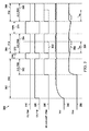
図2は、例示の実施例に従った高速モード遷移パワーコンバータ200を示す概略図である。高速モード遷移パワーコンバータ200は、図1の高速モード遷移パワーコンバータ138の特定の実施例を含み、基板202上に任意で(全体的に又は部分的になど)形成される。概して説明される高速モード遷移パワーコンバータ200は、モード信号生成器210、モードコントローラ220、センサ228、PFMコントローラ240、PWMコントローラ250、パワー出力段260(例えば、電圧出力Voutを生成するように動作し得る)、及び補助電圧出力段270(例えば、補助出力電圧Vauxを生成するように動作し得る)を含む。
FIG. 2 is a schematic view showing a high-speed mode
モード信号生成器210は、PFMモードでの又はPWMモードでの電圧出力でオペレーションを選択するように動作し得る信号を生成する。モード信号生成器は、(図1に図示するような)CPU 112など、プロセッサからの信号に応答して動作され得る。種々の実施例において、プロセッサは、電子システム129が受信モードにあるか又は送信モードにあるかを判定するネットワークインタフェースプロトコルなどの通信ネットワークプロトコルに応答して、モード信号生成器210に信号を送る。例えば、モード信号生成器210は、トランシーバの選択された送信/受信モードに応答して、高速モード遷移パワーコンバータ200の動作モードを選択する。従って、高速モード遷移パワーコンバータ200は、特定の動作モードに関連付けられる規格に従って動作電力を供給するように動作し得る。
The
モード信号生成器210は、モードコントローラ220に結合される。例えば、モードコントローラ220は、遷移のタイミングを制御するように、及び制御信号をバッファするように動作し得る。任意選択の電流センサ230は、動作負荷電流を測定するように動作し得る。モード信号生成器210は、任意選択で、センサ228に応答する(例えば、動作電流負荷に応答して動作モードを選択するように動作し得る)。センサ228は、電流センサ230及びゼロ交差検出器232を含み、これらはいずれも、パワー出力段260の制御スイッチに制御情報を提供する。
The
更に特定して言えば、PFMコントローラ240は、PFMコントローラ245、スイッチ247、及び、パワー段260を駆動するロジックユニット249を含む。PFMコントローラ240において、PFMコントローラ245は、電圧基準Vref及び電圧出力Voutに、及び、パワー段260を駆動するロジックユニット249へのPFMコントローラ245の接続を制御するスイッチ247に結合される。PWMコントローラ255は、電圧基準Vrefとスイッチ251とに結合され、スイッチ251は、電圧出力VoutへのPWMコントローラ255の接続を制御する。モードコントローラ220は、PFMコントローラ240のスイッチ247に結合される。例えば、高速モード遷移パワーコンバータ200がPFMモードで動作しているとき、スイッチ247は、PFMコントローラ245の出力をロジックユニット249の入力に選択的に結合するように動作し得る。
More specifically, the
同様に、PWMコントローラ250は、スイッチ251、スイッチ253、PWMコントローラ255、スイッチ257、スイッチ258、及び、補助パワー段270を駆動するロジックユニット259を含む。PWMコントローラ255はスイッチ253にも結合され、スイッチ253は、補助出力電圧VauxへのPWMコントローラ255の接続を制御する。PWMコントローラ255はスイッチ257にも結合され、スイッチ257は、PFMコントローラ240のロジックユニット249へのPWMコントローラ255の接続を制御する。PWMコントローラ255はスイッチ258にも結合され、スイッチ258は、ロジックユニット259へのPWMコントローラ255の接続を制御する。モードコントローラ220は、PWMコントローラ250のスイッチ251、253、257、及び258に結合される。
Similarly, the
例えば、スイッチ251は、高速モード遷移パワーコンバータ200がPWMモードで動作しているとき、電圧出力Voutを、PWMコントローラ255の入力に選択的に結合するように動作し得る。スイッチ257は、PWMコントローラ255の出力を、パワー段260を駆動するロジックユニット249の入力に選択的に結合するように動作し得る。PWMモードに遷移する速度を増大させるため、スイッチ258は、PWMモードに入る前にPWMコントローラ255の出力をロジックユニット249の入力に選択的に結合する(これは、補助電圧源270をアクティブにする)ように動作し得る。スイッチ253は、(スイッチ251が開である間)閉じられ、これは、(補助電圧生成器270により生成される)Vaux信号をPWMコントローラ255の入力に結合する。(例えば、静止モード又はPFMモードで動作している間)PWMモードに入る前にVaux信号をPWMコントローラに結合することで、高速モード遷移パワーコンバータ250の既存の動作モードを実質的に中断することなく、PWMコントローラ250制御ループの安定化が開始される。
For example, the
パワー出力段260はパワーFETスイッチ265を含み、パワーFETスイッチ265は、電圧源をインダクタLなどのエネルギーストレージ要素の第1の端子に選択的に結合するように動作し得る。インダクタLの第2の端子が、キャパシタCのハイサイドと出力電圧ノードVoutとに結合される。負荷が、任意選択でノードVoutに結合され、任意選択で電流センサ230を含む。パワースイッチ265は、ロジックユニット249の出力に応答して駆動される。
The
補助電圧出力段270はFETスイッチ275を含む。パワーFETスイッチ275は、出力パワー段260に存在する受動構成要素の周波数応答をエミュレートするように動作し得るネットワークの入力端子に電圧源を選択的に結合するように動作し得る。例えば、バックコンバータを制御するとき、「LC」周波数応答がエミュレートされる。受動ネットワークは、第1のレジスタR1及び第2のレジスタR2を含む。第1のキャパシタC1が、レジスタネットワークの中央ノードと接地との間(例えば、R1とR2の間)に結合される。第2のキャパシタC2が、レジスタネットワークの出力端子と接地との間に結合される。C2の出力端子は、補助電圧出力Vauxを提供する。例えば、構成要素R1、R2、C1、及びC2は、PWMコントローラ250(及びPFMコントローラ240)と同じ基板上に形成され、フィードバック信号Vauxを含むPWMコントローラ250のループが安定であるように選択される。パワースイッチ275は、供給電圧がVauxに変換されるように、PWMコントローラ250のロジックユニット259の出力に応答して駆動される。用いられないとき、パワースイッチ275は、供給電圧が分圧器の中央ノードに結合されず、従って電力消費が低減されるように、任意選択で開状態に置かれる。
The auxiliary
オペレーションにおいて、モード信号生成器210及び任意選択の電流センサ230は、入力信号をモードコントローラ220に提供し、これは、入力信号に応答してPFMコントローラ240及びPWMコントローラ250のスイッチを作動させる(開閉するなど)。PFMモード(PFMオンリーモードなど)で動作させるため、モードコントローラ220は、(例えば、PWMコントローラ250の他のスイッチが開のままである間)PFMコントローラ240のスイッチ247を閉じるようシグナリングする。従って、PFMコントローラ240のロジックユニット249は、PFMコントローラ245により生成されるPFMモード信号に応答して出力電圧Voutを制御するように動作し得る。
In operation, the
補助PWMモードにおいて、PFMモードでの動作からPWMモードへの高速遷移を促進するために、PWMモードがPFMモードと並列に動作される。補助PWMモードに入るため、モードコントローラ220は、PWMコントローラ250のスイッチ253及び258を閉じるようにシグナリングする。スイッチ253及び258が閉である(及びスイッチ251及び257が開である)とき、PWMコントローラ255は、補助電圧VauxをVrefの電圧と(例えば、Vrefの電圧に対して)比較するように配され、それに応答して、補助電圧Vaux(これは、補助電圧出力段270により出力される)をレギュレートするための制御信号を生成する。補助PWMモード(補助電圧出力段270が動作するモード)において動作することは、パワー出力段260がオペレーションのPWMモードで動作し続けるとき消費し得るよりも実質的に少ない電力を消費する。例えば、電力消費の低減の結果、制限された電力消費アプリケーションにおいて(バッテリー電力から動作するときなど)動作時間が増大される。
In the auxiliary PWM mode, the PWM mode is operated in parallel with the PFM mode in order to promote a high-speed transition from the operation in the PFM mode to the PWM mode. To enter the auxiliary PWM mode, the
PFMでの動作から(例えば標準の)PWMモードでの動作へ遷移するため、モードコントローラ220は、PWMコントローラ250のスイッチ251及び257を閉じる(及びスイッチ253及び258が開である)ようにシグナリングする。Vauxの電圧は、典型的に、(a)スイッチ253及び258が閉であり、スイッチ251及び257が開であるとき、及び(b)スイッチ253及び258が開であり、スイッチ251及び257が閉であるときの両方のケースにおいて、PWMコントローラ250の動作ポイントが同じ値にセトリングするように、Voutの公称電圧と同じ電圧であるように選択される。先に述べたケースの動作ポイントは、オンチップ構成要素の形成におけるミスマッチに起因して、わずかに異なり得る。例えば、同様の動作ポイントを有することが、動作モード間の高速遷移を促進する。スイッチ251及び257が閉であるとき、PWMコントローラ255は、出力電圧VoutをVrefの電圧に対して比較するように配され、これに応答して、出力電圧Voutをレギュレートするために制御信号を生成する。
To transition from operation in PFM to operation in (eg, standard) PWM mode,
モードコントローラ220が、PWMコントローラ250のスイッチ251及び257を閉じさせるとき(又は、例えば、そのすぐ後)、モードコントローラ220は、PFMコントローラ240のスイッチ247を開き、これは、パワー出力段260の制御をPWMコントローラ250に移す。PFMからPWMへの遷移が完了した後、補助PWMモードは(例えば任意選択で)、スイッチ253及び258を開く(及び補助電圧源270をシャットダウンする)ようにシグナリングするモードコントローラ220により開放される(disengaged)。モード信号生成器210からモードコントローラ220への入力が、高速モード遷移パワーコンバータ200がPWMモードでの動作からPFMモードでの動作に戻って遷移することを示すとき、モードコントローラ220は、スイッチ247を閉じるようにシグナリングし、及び(例えば、ほぼ同時に)スイッチ251及び257を開くようにシグナリングする。
When the
図3は、例示の実施例に従った高速モード遷移パワーコンバータのスイッチング波形及び出力電圧を図示する波形図である。概して説明される波形図300は、高速モード遷移パワーコンバータの種々の信号の、経時的な電圧及び状態の変化を図示する。波形図300は、イネーブルPFM信号(EN_PFM)310、イネーブルPWM信号(EN_PWM)320、イネーブル補助PWM信号(EN_AUXILIARY_PWM)330、出力電圧(Vout)340、及び補助電圧(Vaux)350を含む。イネーブル信号EN_PFM310、EN_PWM320、及びEN_AUXILIARY_PWM330は、図2に図示した高速モード遷移パワーコンバータ200のモード信号生成器210により生成されるものなど、デジタル信号を表す。
FIG. 3 is a waveform diagram illustrating a switching waveform and an output voltage of a high-speed mode transition power converter according to an exemplary embodiment. A generally described waveform diagram 300 illustrates changes in voltage and state over time for various signals of a high speed mode transition power converter. The waveform diagram 300 includes an enable PFM signal (EN_PFM) 310, an enable PWM signal (EN_PWM) 320, an enable auxiliary PWM signal (EN_AUXILIARY_PWM) 330, an output voltage (Vout) 340, and an auxiliary voltage (Vaux) 350. The enable signals EN_PFM310, EN_PWM320, and EN_AUXILIALY_PWM330 represent digital signals such as those generated by the
EN_PFM310、EN_PWM320、及びEN_AUXILIARY_PWM330の各々に対する低電圧は「オフ」状態を表し、高電圧は「オン」状態を表す。波形図300における垂直線は、高速モード遷移パワーコンバータ138及び/又は高速モード遷移パワーコンバータ200のオペレーションの間生じる、特定の時間期間を区切る。
A low voltage for each of EN_PFM310, EN_PWM320, and EN_AUXILIALY_PWM330 represents an "off" state and a high voltage represents an "on" state. Vertical lines in waveform diagram 300 delimit specific time periods that occur during the operation of the fast mode transition power converter 138 and / or the fast mode
出力電圧(Vout)340及び補助電圧(Vaux)350は、図2に図示した、それぞれ、パワー出力段260及び補助電圧出力段270により生成されるような経時的なこれらの電圧の大きさを表す。パワー出力段260は、パワー出力段260が出力電圧(Vout)を生成し始めるように、EN_PFM310の正の遷移によりイネーブルされる。Vout340は、PFMモード362の初期部分の間上昇し、PFMモード362の後の部分の間PFMコントローラ240によってレギュレーションが達成されるとき、低閾値電圧と高閾値電圧との間で変動する。
The output voltage (Vout) 340 and the auxiliary voltage (Vaux) 350 represent the magnitudes of these voltages over time as generated by the
PWMモードに入ることを予期する際(例えば、トランシーバコントローラによって決まる)、EN_AUXILIARY_PWM330がアサートされ、補助PWMモード(AUX_PWM期間372など)がエンターされる。EN_AUXILIARY_PWM330がアサートされるとき、Vaux350は、Vout340のターゲット電圧にほぼ等しい電圧まで上昇する。Vaux350がこのほぼ等しいターゲット電圧まで上昇するとき、PWMコントローラ250によってレギュレーションが達成される。
When anticipating entering PWM mode (eg, determined by the transceiver controller), EN_AUXILIALY_PWM330 is asserted and the auxiliary PWM mode (such as AUX_PWM period 372) is entered. When EN_AUXILIARY_PWM330 is asserted, the
補助PWMモードの間、PWMコントローラ250によってレギュレーションが達成された後(又は、例えば、充分な時間長の後)、EN_PFM310がデアサートされ(例えば、ネゲート(無効に)され)、EN_PWM320がアサートされる。このとき(例えば、ほぼこの頃)、PWMコントローラ250は(基準としてVaux350を用いて)、パワー出力段260をレギュレートするために用いられる。従って、PWMコントローラ250のオペレーション(フィードバック安定性を達成することなど)は、電圧Vout340をレギュレートするために(例えば、まだ)結合されることなく、ブートストラップされる。
During the auxiliary PWM mode, EN_PFM310 is deasserted (eg, negated) and EN_PWM320 is asserted after regulation has been achieved by the PWM controller 250 (or, for example, after a sufficient time). At this time (for example, about this time), the PWM controller 250 (using the
EN_AUXILIARY_PWM330がデアサートされる頃、PWMモードがエンターされる(及び補助PWMモードが励起される)。EN_AUXILIARY_PWM330がデアサートされるとき、PWMコントローラ250は、(例えば選択的に結合される)Vout340を基準として用いてパワー出力段260をレギュレートする。一実施例において、補助電圧出力段270がもはやレギュレートされず、従ってVaux350が下がり始めるように、このとき、信号Vaux350は、PWMコントローラ255の入力から結合解除される。
When EN_AUXILIARY_PWM330 is deasserted, the PWM mode is entered (and the auxiliary PWM mode is excited). When EN_AUXILIALY_PWM330 is deasserted, the
PWMモードを出ることを予期する際(例えば、トランシーバコントローラによって決まる)、EN_PWM320がデアサートされ、PFMモード(PFM期間364など)がエンターされる。EN_PWM320がデアサートされるとき、上述のようにPFMモードがエンターされるように、EN_PFM310がアサートされる。このとき信号EN_AUXILIARY_PWMが任意選択でアサートされるか、又は時間Tflex(時間フレックス)396の後(例えば、時間Tflex396にわたって電力消費を低減するために)アサートされる。Vout340が2つの閾値電圧間で変動するとき、PFMコントローラ240によってレギュレーションが達成される。
When anticipating exiting the PWM mode (eg, determined by the transceiver controller), EN_PWM320 is deasserted and the PFM mode (
次のPWMモードに入ることを予期する際、上述のようにPWMコントローラ259をブートストラップするために補助PWMモードが用いられる。(例えば、必ずしも)必要とされないとき(PFMモードの間など)PWMコントローラをオフにすることは電力を節約するが、PWMコントローラ250を再度アクティブにするときPWMコントローラ250をブートストラップするために付加的な時間が必要となる。従って、PWMコントローラ250をブートストラップするために補助PWMモードを用いることで、そうでなければPWMコントローラ250をブートストラップするために必要とされる時間量が低減され、高速モード遷移を提供することによりシステムの全体的な電力消費が低減される。
When anticipating entering the next PWM mode, the auxiliary PWM mode is used to bootstrap the
従って、PFM時間期間362、364、及び366は、高速モード遷移パワーコンバータ138がPFMモードで動作しているように、イネーブル信号EN_PFM310がオンである期間である。PWM時間期間372及び374は、イネーブル信号EN_PWM320がイネーブルされ、高速モード遷移パワーコンバータ138がPWMモードで動作している期間である。AUX_PWM時間期間382、384、及び386は、イネーブル信号EN_AUXILIARY_PWM330がイネーブルされ、高速モード遷移パワーコンバータ138が補助PWMモードで動作しており、しばしば同時に高速モード遷移パワーコンバータ138がPFMモードで動作している期間である。
Therefore, the
従って、補助電圧出力段270(図2に図示される)によって提供される補助電圧Vaux350は、PFMモードでの高速モード遷移パワーコンバータ138のオペレーションからPWMモードでのオペレーションへの遷移の間、Vout340の急速な電力セトリングを提供するように動作し得る。
Therefore, the auxiliary voltage Vaux350 provided by the auxiliary voltage output stage 270 (shown in FIG. 2) is the
Tflex(フレキシブル時間)時間期間396は、PFM364の第1の部分におけるEN_PFM310のアサーションの後、イネーブル信号EN_AUXILIARY_PWM330が任意選択で一層長い時間オフのままとなる(例えば、EN_AUXILIARY_PWM330の部分334により示されるような)時間期間である。補助電圧(Vaux)波形の部分354は、イネーブル信号EN_AUXILIARY_PWMが任意選択で時間期間396の間オフのままであるとき補助電圧出力段270(図2に図示される)によって達成される補助電圧(Vaux)の一層低いレベルを表す。
The Tflex (flexible time)
図4は、例示の実施例に従った高速モード遷移パワーコンバータの、スイッチング波形、出力電圧、及び電流を図示する波形シミュレーションである。概して説明される波形図400は、イネーブルPFM信号(EN_PFM)410、イネーブルPWM信号(EN_PWM)420、イネーブル補助PWM信号(EN_AUXILIARY_PWM)430、出力電圧(Vout)440、補助電圧(Vaux)450、負荷電流460、インダクタ電流470、及び供給電流480の波形を図示する。 FIG. 4 is a waveform simulation illustrating the switching waveform, output voltage, and current of a high-speed mode transition power converter according to an exemplary embodiment. The generally described waveform diagram 400 shows an enable PFM signal (EN_PFM) 410, an enable PWM signal (EN_PWM) 420, an enable auxiliary PWM signal (EN_AUXILIARY_PWM) 430, an output voltage (Vout) 440, an auxiliary voltage (Vaux) 450, and a load current. The waveforms of 460, inductor current 470, and supply current 480 are illustrated.
波形図400は、PFMモードにおけるオペレーションからPWMモードへの遷移に応答する高速モード遷移パワーコンバータ138の内部電流の出力電圧及び測定値のシミュレーション結果を図示する。(EN_AUXILIARY_PWM)信号430は、補助PWMモードの間のVaux450レギュレーション制御信号の動作を表す。初期的に、イネーブルPFM信号(EN_PFM)410が、シミュレーションの開始時にアサートされる。約500.0マイクロ秒に対応する時間に、イネーブルPWM信号(EN_PWM)420がアサートされる。約504.0マイクロ秒(「PFMからPWMへの遷移時間ポイント」)において、高速モード遷移パワーコンバータがPFMモードからPWMモードへ遷移するようにイネーブルPFM信号(EN_PFM)410がデアサートされる。PFMからPWMへの遷移時間ポイントにおいて、(例えば、フィードバック信号として、VauxではなくVoutを用いることにより)レギュレーションの一時的欠落が、出力電圧(Vout)440及び補助電圧(Vaux)450両方においてスパイクを生じさせる。スパイクの程度は、フィードバックループが安定化し、現在レギュレートされている電圧両方が約511.0マイクロ秒において(例えば比較的短い時間期間において)安定したPWMモードパターンにセトリングするように、低減する。約511.0マイクロ秒以降(その間、依然としてスイッチングされている一方でレギュレーションの欠落などに起因して、補助電圧Vaux450が上昇する)、出力電圧(Vout)440は、(例えば、フィードバック信号としてVoutを用いることにより)約1.8ボルトの電圧を維持するようにレギュレートされる。 The waveform diagram 400 illustrates the simulation results of the output voltage and the measured value of the internal current of the high-speed mode transition power converter 138 in response to the transition from the operation in the PFM mode to the PWM mode. The (EN_AUXILIARY_PWM) signal 430 represents the operation of the Vaux450 regulation control signal during the auxiliary PWM mode. Initially, the enable PFM signal (EN_PFM) 410 is asserted at the start of the simulation. The enable PWM signal (EN_PWM) 420 is asserted at a time corresponding to about 500.0 microseconds. At about 504.0 microseconds (“PFM to PWM transition time point”), the enable PFM signal (EN_PFM) 410 is deasserted so that the fast mode transition power converter transitions from PFM mode to PWM mode. At the transition time point from PFM to PWM, a temporary lack of regulation (eg, by using Vout instead of Vaux as the feedback signal) spikes at both output voltage (Vout) 440 and auxiliary voltage (Vaux) 450. Give rise. The degree of spikes is reduced so that the feedback loop stabilizes and both currently regulated voltages settle to a stable PWM mode pattern at about 511.0 microseconds (eg, for a relatively short time period). After about 511.0 microseconds (during which the auxiliary voltage Vaux450 rises due to lack of regulation while still being switched), the output voltage (Vout) 440 (eg, Vout as a feedback signal). (By use) regulated to maintain a voltage of about 1.8 volts.
同様に、(例えば、図2に図示されるパワー出力段260のインダクタLにおける)インダクタ電流470は、PFMからPWMへの遷移時間ポイントにおいて流れ始め、(たとえ、約510.0マイクロ秒において生じる負荷電流460における増大がある場合でも)約511.0マイクロ秒までに安定したPWMモードパターンにセトリングする。
Similarly, the inductor current 470 (for example, in the inductor L of the
供給電流480は、インダクタ電流470によりソースされる。供給電流480における小さなスパイクがPFMからPWMへの遷移時間ポイントにおいて生じ、約511.0マイクロ秒までにセトリングする。従って、イネーブル補助PWM信号(EN_AUXILIARY_PWM)430に応答して、例えば補助電圧出力段270により生成されるような、補助電圧(Vaux)450の存在は、高速モード遷移パワーコンバータ138に、PFMモードからPWMモードへ急速に遷移させ、電力セトリングが約7マイクロ秒内に起こる。従って、出力電圧段の出力電圧は、第2の時間期間の開始後、約8マイクロ秒未満の時間内にレギュレートされる(例えば、出力電圧は、パワー出力段により生成される電力における約1パーセント未満の変動でレギュレートされる)。
The
図5は、例示の実施例に従った、補助電圧出力段を備えたパワーコンバータのオペレーションの方法を説明するフローチャートである。プログラムフロー500は、補助電圧出力段を備えたパワーコンバータがPFMモードで動作し始めるオペレーション510において始まる。プログラムフローはオペレーション512に続く。
FIG. 5 is a flowchart illustrating a method of operating a power converter with an auxiliary voltage output stage according to an exemplary embodiment. The
オペレーション512において、パワーコンバータの補助電圧出力段は、(任意選択で)PWMモードへの潜在的な遷移のための準備において動作し始める。このような準備には、補助電圧出力段における回路要素の電力供給されていない部分に電力を印加することが含まれる。種々の実施例において(例えば、電力消費のレートが現在は制限要因ではない応用例などにおいて)、パワーコンバータの補助電圧出力段は、「ウォーム(warm)」状態でパワーアップされたままである。ウォーム状態の間、全ての電力が補助電圧出力段から取り除かれるわけではない(例えば、これは、PFM及びPWMモード間で切り替わるときレイテンシーを低減する)。プログラムフローはオペレーション514に進む。
In
オペレーション514において、補助電圧出力段のモードコントローラは、モード信号生成器から信号を受信する。信号モード生成器は、補助PWM(AUX_PWM)モードに遷移するために信号を生成する。例えば、こういった信号は、電子通信システムのオペレーションモード(送信または受信など)の指示を提供する、プロセッサからの信号に応答して生成される。プロセッサから信号は、任意選択で、履歴の伝送パターンに応答して生成され(例えば、経時的な送信及び受信モードが、データベースにストアされたデータによって表されるなど)、及び/又は所定のタイマー値の満了に応答して生成される。プログラムフローはオペレーション516に続く。
In
オペレーション516において、補助電圧出力段を備えたパワーコンバータのモードコントローラは、動作を継続するための信号が受信されたか否かを判定する。受信された場合、プログラムフローはオペレーション520に続く。受信されていない場合、プログラムフローは終了する。プログラムフローは、任意選択で、オペレーション510におけるプログラムフローの開始で再開される。
In
オペレーション520において、補助電圧出力段を備えたパワーコンバータのモードコントローラは、PWMモードでの動作を可能にするための信号が受信されたか否かを判定する。受信された場合、プログラムフローはオペレーション522に続く。受信されない場合、プログラムフローは待機する(又は、例えば、オペレーション510に進むことによりリスタートする)。
In
オペレーション522において、補助電圧出力段を備えたパワーコンバータのモードコントローラは、補助PWM(AUX_PWM)モードが動作中であるか否かを判定する。動作中である場合、プログラムフローはオペレーション530に続く。動作中でない場合、プログラムフローはオペレーション524に進む。
In
オペレーション524において、補助電圧出力段を備えたパワーコンバータは、補助PWM(AUX_PWM)モードで動作し始める(これは、例えば、PWMモードがエンターされる前にPWMコントローラのフィードバックループを安定化させることによって、PWMコントローラの初期化のレイテンシーを低減する)。プログラムフローはオペレーション530に続く。
In
オペレーション530において、補助電圧出力段を備えたパワーコンバータは、PWMモードで動作し始め、及び同時に又はそのすぐ後、補助電圧出力段を備えたパワーコンバータは、PFMモードでの動作を停止する。プログラムフローはオペレーション532に続く。
In
オペレーション532において、補助電圧出力段を備えたパワーコンバータは、任意選択で、プロセッサからの信号に応答して補助PWM(AUX_PWM)モードでの動作を停止する。例えば、補助PWMモードの動作を停止することは、そうでなければAUX_PWMモードで用いられる構成要素を給電するために用いられる電力を節約する。プログラムフローはオペレーション534に進む。
In
オペレーション534において、補助電圧出力段を備えたパワーコンバータのモードコントローラは、モード信号生成器から信号を受信する。プログラムフローはオペレーション536に続く。
In
オペレーション536において、補助電圧出力段を備えたパワーコンバータのモードコントローラは、動作を継続するための信号が受信されたか否かを判定する。受信された場合、プログラムフローはオペレーション538に続く。受信されなかった場合、プログラムフローは終了する。プログラムフローは、任意選択で、オペレーション510におけるプログラムフローの再開で再開され(リスタートされるなど)得る。
In
オペレーション538において、補助電圧出力段を備えたパワーコンバータのモードコントローラは、PFMモードでの動作を可能にする信号が受信されたか否かを判定する。受信された場合、プログラムフローはオペレーション540に続く。受信されなかった場合、プログラムフローは、オペレーション534に進む。
In
オペレーション540において、補助電圧出力段を備えたパワーコンバータは、PFMモードで動作し始め、同時に又はそのすぐ後、補助電圧出力段を備えたパワーコンバータは、PWMモードでの動作を停止する。プログラムフローはオペレーション512に続く。
In
種々の実施例において、上述の構成要素は、内部的に又は外部的に、ハードウェア又はソフトウェアにおいて実装され得、及び他のモジュール及び本願において図示するような構成要素と機能性を共有し得る。 In various embodiments, the components described above may be implemented internally or externally in hardware or software, and may share functionality with other modules and components as illustrated herein.
本発明の特許請求の範囲内で、説明した例示の実施例に変形が成され得、他の実施例が可能である。 Within the scope of the claims of the present invention, modifications can be made to the illustrated examples described, and other examples are possible.
Claims (17)
第1の電圧出力を生成するように構成されるパワー出力段と、
第2の電圧出力を生成するように構成される補助パワー出力段と、
前記パワー出力段がパルス周波数変調(PFM)モードで動作する第1の時間期間の間に前記パワー出力段により生成される前記第1の電圧出力に応答して前記パワー出力段を制御するように構成されるPFMコントローラと、
前記補助パワー出力段がパルス幅変調(PWM)モードで動作する第2の時間期間の間に前記補助パワー出力段により生成される前記第2の電圧出力に応答して前記補助パワー出力段を制御し、前記第2の時間期間と前記第1の時間期間とに続く第3の時間期間の間に前記パワー出力段を制御するように構成されるPWMコントローラと、
を含み、
前記第1の時間期間が第1の継続期間を有し、前記第2の時間期間が第2の継続期間を有し、前記第1の継続期間が前記第2の継続期間よりも大きく、前記PFMコントローラが前記パワー出力段を制御して前記第1の電圧出力を生成し、同時に、前記PWMコントローラが前記補助パワー出力段を制御して前記第2の電圧出力を生成するように、前記第1の時間期間の一部のみが前記第2の時間期間と同時である、コンバータ。 It ’s a converter,
A power output stage configured to generate a first voltage output,
An auxiliary power output stage configured to generate a second voltage output,
To control the power output stage in response to the first voltage output generated by the power output stage during the first time period during which the power output stage operates in pulse frequency modulation (PFM) mode. The configured PFM controller and
Control the auxiliary power output stage in response to the second voltage output generated by the auxiliary power output stage during a second time period during which the auxiliary power output stage operates in pulse width modulation (PWM) mode. A PWM controller configured to control the power output stage during a third time period following the second time period and the first time period .
Including
The first time period has a first duration, the second time period has a second duration, and the first duration is greater than the second duration. The second voltage output is generated so that the PFM controller controls the power output stage to generate the first voltage output, and at the same time, the PWM controller controls the auxiliary power output stage to generate the second voltage output. A converter in which only a portion of one time period is simultaneous with the second time period.
前記第1の時間期間と第2の時間期間とが実質的に同じ時間に終了する、コンバータ。 The converter according to claim 1 .
A converter in which the first time period and the second time period end at substantially the same time.
前記第2の時間期間が前記第1の時間期間が始まる後に始まる、コンバータ。 The converter according to claim 2 .
A converter in which the second time period begins after the first time period begins.
前記PWMコントローラがフィードバック信号に応答して前記パワー出力段と前記補助パワー出力段とを制御し、
前記フィードバック信号が、前記第2の時間期間の間に前記第2の電圧出力に基づき、前記第3の時間期間の間に前記第1の電圧出力に基づく、コンバータ。 The converter according to claim 1 .
The PWM controller controls the power output stage and the auxiliary power output stage in response to the feedback signal.
A converter in which the feedback signal is based on the second voltage output during the second time period and based on the first voltage output during the third time period.
前記第1の時間期間が前記第3の時間期間の後に始まる、コンバータ。 The converter according to claim 1 .
A converter in which the first time period begins after the third time period.
第1の継続期間を有する第1の時間期間の間にパルス周波数変調(PFM)モードでパワー出力段を制御することと、
第2の継続期間を有する第2の時間期間の間にパルス幅変調(PWM)モードで補助パワー出力段を制御することと、
を含み、
前記第1の継続期間が前記第2の継続期間よりも大きく、前記パワー出力段が第1の電圧出力を生成し、同時に、前記補助パワー出力段が第2の電圧出力を生成するように、前記第1の時間期間の一部のみが前記第2の時間期間に重なる、方法。 The way
Controlling the power output stage in pulsed frequency modulation (PFM) mode during the first time period with the first duration,
Controlling the auxiliary power output stage in pulse width modulation (PWM) mode during a second time period with a second duration, and
Including
The first duration is greater than the second duration so that the power output stage produces a first voltage output and at the same time the auxiliary power output stage produces a second voltage output. A method in which only a portion of the first time period overlaps the second time period.
第3の時間期間の間に前記PWMモードで前記パワー出力段を制御することを更に含み、前記第3の時間期間が前記第1又は第2の時間期間のどちらとも重ならない、方法。 The method according to claim 6 .
A method further comprising controlling the power output stage in the PWM mode during a third time period, wherein the third time period does not overlap with either the first or second time period.
前記第3の時間期間が前記第1の時間期間の後に起こる、方法。 The method according to claim 7 .
A method in which the third time period occurs after the first time period.
前記第1の時間期間と前記第2の時間期間とが実質的に同じ時間に完了する、方法。 The method according to claim 8 .
A method in which the first time period and the second time period are completed at substantially the same time.
前記第1の時間期間と前記第2の時間期間とが異なる時間に始まる、方法。 The method according to claim 9 .
A method in which the first time period and the second time period start at different times.
前記第3の時間期間の後に起こる第4の時間期間の間に前記PFMモードで前記パワー出力段を制御することと、
前記第3の時間期間の後に起こる第5の時間期間の間に前記PWMモードで前記補助パワー出力段を制御することと、
を更に含み、
少なくとも前記第4の時間期間の一部が前記第5の時間期間に重なる、方法。 The method according to claim 9 .
Controlling the power output stage in the PFM mode during a fourth time period that occurs after the third time period.
Controlling the auxiliary power output stage in the PWM mode during a fifth time period that occurs after the third time period.
Including
A method in which at least a part of the fourth time period overlaps with the fifth time period.
前記第4の時間期間と前記第5の時間期間とが、実質的に同じ時間に完了するが、異なる時間に始まる、方法。 The method according to claim 11 .
A method in which the fourth time period and the fifth time period are completed at substantially the same time, but start at different times.
前記第5の時間期間が前記第4の時間期間の後に始まる、方法。 The method according to claim 12 .
A method in which the fifth time period begins after the fourth time period.
前記第4の時間期間と前記第5の時間期間とが実質的に同じ時間に開始して停止する、方法。 The method according to claim 11 .
A method in which the fourth time period and the fifth time period start and stop at substantially the same time.
送信モードでデータを送信し、受信モードでデータを受信する入力/出力(I/O)ポートと、
前記I/Oポートに電力を供給するパワーコンバータと、
を含み、
前記パワーコンバータが、
第1の電圧出力を生成するパワー出力段と、
第2の電圧出力を生成する補助パワー出力段と、
前記I/Oポートが前記受信モードで動作する第1の時間期間の間に前記パワー出力段により生成される前記第1の電圧出力に応答して前記パワー出力段を制御するパルス周波数変調(PFM)コントローラと、
第2の時間期間の間に前記補助パワー出力段により生成される前記第2の電圧出力に応答して前記補助パワー出力段を制御し、前記第2の時間期間と前記第1の時間期間とに続く第3の時間期間の間に前記パワー出力段を制御するパルス幅変調(PWM)コントローラと、
を含み、
前記第1の時間期間が第1の継続期間を有し、前記第2の時間期間が第2の継続期間を有し、前記第1の継続期間が前記第2の継続期間よりも大きく、前記PFMコントローラが前記パワー出力段を制御して前記第1の電圧出力を生成し、同時に、前記PWMコントローラが前記補助パワー出力段を制御して前記第2の電圧出力を生成するように、前記第1の時間期間の一部のみが前記第2の時間期間と同時である、システム。 It's a system
Input / output (I / O) ports that send data in transmit mode and receive data in receive mode,
A power converter that supplies power to the I / O port,
Including
The power converter
A power output stage that produces a first voltage output,
An auxiliary power output stage that produces a second voltage output,
Pulse frequency modulation (PFM) that controls the power output stage in response to the first voltage output generated by the power output stage during the first time period during which the I / O port operates in the receive mode. ) Controller and
During the second time period, the auxiliary power output stage is controlled in response to the second voltage output generated by the auxiliary power output stage, and the second time period and the first time period A pulse width modulation (PWM) controller that controls the power output stage during a third time period following
Including
Said first time period has a first duration, said second time period has a second duration, greater than the first duration is the second duration, the The second voltage output is generated so that the PFM controller controls the power output stage to generate the first voltage output, and at the same time, the PWM controller controls the auxiliary power output stage to generate the second voltage output . A system in which only a portion of one time period is simultaneous with the second time period.
前記第1の時間期間と前記第2の時間期間とが実質的に同じ時間に完了する、システム。 The system according to claim 15 .
A system in which the first time period and the second time period are completed at substantially the same time.
前記第1の時間期間と前記第2の時間期間とが異なる時間に始まる、システム。 The system according to claim 16 .
A system in which the first time period and the second time period start at different times.
Applications Claiming Priority (3)
| Application Number | Priority Date | Filing Date | Title |
|---|---|---|---|
| US14/588,111 | 2014-12-31 | ||
| US14/588,111 US9685863B2 (en) | 2014-12-31 | 2014-12-31 | Fast mode transitions in a power converter |
| PCT/US2015/068313 WO2016109811A1 (en) | 2014-12-31 | 2015-12-31 | Fast mode transitions in a power converter |
Related Child Applications (1)
| Application Number | Title | Priority Date | Filing Date |
|---|---|---|---|
| JP2020200341A Division JP7185374B2 (en) | 2014-12-31 | 2020-12-02 | Fast mode transitions in power converters |
Publications (3)
| Publication Number | Publication Date |
|---|---|
| JP2018500874A JP2018500874A (en) | 2018-01-11 |
| JP2018500874A5 JP2018500874A5 (en) | 2019-01-31 |
| JP6804454B2 true JP6804454B2 (en) | 2020-12-23 |
Family
ID=56165449
Family Applications (2)
| Application Number | Title | Priority Date | Filing Date |
|---|---|---|---|
| JP2017535449A Active JP6804454B2 (en) | 2014-12-31 | 2015-12-31 | High-speed mode transition in power converter |
| JP2020200341A Active JP7185374B2 (en) | 2014-12-31 | 2020-12-02 | Fast mode transitions in power converters |
Family Applications After (1)
| Application Number | Title | Priority Date | Filing Date |
|---|---|---|---|
| JP2020200341A Active JP7185374B2 (en) | 2014-12-31 | 2020-12-02 | Fast mode transitions in power converters |
Country Status (4)
| Country | Link |
|---|---|
| US (4) | US9685863B2 (en) |
| JP (2) | JP6804454B2 (en) |
| CN (2) | CN107112900B (en) |
| WO (1) | WO2016109811A1 (en) |
Families Citing this family (6)
| Publication number | Priority date | Publication date | Assignee | Title |
|---|---|---|---|---|
| JP6065808B2 (en) * | 2013-10-24 | 2017-01-25 | 三菱電機株式会社 | Semiconductor device and semiconductor module |
| US9685863B2 (en) * | 2014-12-31 | 2017-06-20 | Texas Instruments Incorporated | Fast mode transitions in a power converter |
| US9634569B1 (en) * | 2015-10-14 | 2017-04-25 | Dialog Semiconductor (Uk) Limited | DC-to-DC output current sensing |
| CN106549578B (en) * | 2016-12-21 | 2019-10-11 | 湖南国科微电子股份有限公司 | Multi-mode power source managing system |
| US11177737B2 (en) * | 2019-07-19 | 2021-11-16 | Texas Instruments Incorporated | Switching control for power converters |
| CN111509978A (en) * | 2020-05-28 | 2020-08-07 | 长沙学院 | DC-DC conversion device and power management system |
Family Cites Families (26)
| Publication number | Priority date | Publication date | Assignee | Title |
|---|---|---|---|---|
| JPH01238458A (en) * | 1988-03-18 | 1989-09-22 | Fujitsu Denso Ltd | Switching power source device |
| JP2000324835A (en) * | 1999-05-17 | 2000-11-24 | Sony Corp | Multi-output power supply |
| JP3647811B2 (en) * | 2002-01-22 | 2005-05-18 | 東北パイオニア株式会社 | DC-DC converter circuit |
| JP4667836B2 (en) * | 2004-11-26 | 2011-04-13 | 株式会社リコー | Switching regulator and switching regulator output voltage switching method |
| US7148670B2 (en) * | 2005-01-18 | 2006-12-12 | Micrel, Inc. | Dual mode buck regulator with improved transition between LDO and PWM operation |
| US7786714B2 (en) * | 2005-04-01 | 2010-08-31 | Freescale Semiconductor, Inc. | Voltage converter apparatus and method therefor |
| US7504812B2 (en) * | 2005-08-23 | 2009-03-17 | Mediatek, Inc. | Transient behavior while switching between control loops in a switching voltage regulator |
| JP4640985B2 (en) | 2005-12-20 | 2011-03-02 | 富士通セミコンダクター株式会社 | Control circuit and control method for DC-DC converter |
| CN1992493B (en) | 2005-12-30 | 2011-05-18 | 艾默生网络能源系统北美公司 | Resonance DC/DC converter and control method thereof |
| JP4899528B2 (en) * | 2006-02-24 | 2012-03-21 | セイコーエプソン株式会社 | Power supply |
| US20080231115A1 (en) * | 2007-03-16 | 2008-09-25 | Gyuha Cho | Multiple-Output DC-DC Converter |
| US8018743B2 (en) * | 2009-03-05 | 2011-09-13 | Iwatt Inc. | Adaptive control for transition between multiple modulation modes in a switching power converter |
| CN101667019B (en) * | 2009-07-01 | 2012-10-03 | 成都诺奇尔微电子技术有限公司 | Control method and circuit of double-module modulation and mode smooth conversion switching power supply |
| KR101563985B1 (en) * | 2009-09-30 | 2015-10-29 | 엘지디스플레이 주식회사 | Organic electroluminescent display device and method of driving the same |
| US8901908B2 (en) * | 2010-06-08 | 2014-12-02 | Infineon Technologies Austria Ag | Methods and apparatus for DC-DC conversion using digitally controlled adaptive pulse frequency modulation |
| US8937404B1 (en) * | 2010-08-23 | 2015-01-20 | Western Digital Technologies, Inc. | Data storage device comprising dual mode independent/parallel voltage regulators |
| US8487598B2 (en) * | 2010-08-30 | 2013-07-16 | Texas Instruments Incorporated | DC-DC converter with unity-gain feedback amplifier driving bias transistor |
| US8970196B2 (en) | 2011-02-08 | 2015-03-03 | Infineon Technologies Ag | Mode control circuit for DC-DC converter |
| US8896280B2 (en) * | 2011-07-29 | 2014-11-25 | Infineon Technologies Austria Ag | Switching regulator with increased light load efficiency |
| US9479051B2 (en) * | 2011-09-30 | 2016-10-25 | Taiwan Semiconductor Manufacturing Co., Ltd. | Single-inductor multiple-output DC to DC converter |
| KR101877552B1 (en) | 2011-10-12 | 2018-07-12 | 한국전자통신연구원 | DC-DC Converter |
| JP2013153585A (en) * | 2012-01-25 | 2013-08-08 | Asahi Kasei Electronics Co Ltd | Dc-dc converter |
| JP5880239B2 (en) * | 2012-04-13 | 2016-03-08 | 株式会社ソシオネクスト | Power supply device and power supply control method |
| US10698430B2 (en) | 2012-12-19 | 2020-06-30 | Intel Corporation | Method and apparatus of current balancing for multiple phase power converter |
| US9484816B2 (en) * | 2014-06-09 | 2016-11-01 | Infineon Technologies Austria Ag | Controllable on-time reduction for switching voltage regulators operating in pulse frequency modulation mode |
| US9685863B2 (en) * | 2014-12-31 | 2017-06-20 | Texas Instruments Incorporated | Fast mode transitions in a power converter |
-
2014
- 2014-12-31 US US14/588,111 patent/US9685863B2/en active Active
-
2015
- 2015-12-31 CN CN201580071633.4A patent/CN107112900B/en active Active
- 2015-12-31 WO PCT/US2015/068313 patent/WO2016109811A1/en active Application Filing
- 2015-12-31 JP JP2017535449A patent/JP6804454B2/en active Active
- 2015-12-31 CN CN201910948414.XA patent/CN110729897B/en active Active
-
2017
- 2017-05-17 US US15/597,400 patent/US10069419B2/en active Active
-
2018
- 2018-08-31 US US16/118,759 patent/US10811967B2/en active Active
-
2020
- 2020-10-16 US US17/072,217 patent/US11336180B2/en active Active
- 2020-12-02 JP JP2020200341A patent/JP7185374B2/en active Active
Also Published As
| Publication number | Publication date |
|---|---|
| US10069419B2 (en) | 2018-09-04 |
| US9685863B2 (en) | 2017-06-20 |
| CN107112900B (en) | 2019-10-25 |
| US20170250608A1 (en) | 2017-08-31 |
| US10811967B2 (en) | 2020-10-20 |
| US20190089247A1 (en) | 2019-03-21 |
| JP2021048766A (en) | 2021-03-25 |
| CN107112900A (en) | 2017-08-29 |
| CN110729897A (en) | 2020-01-24 |
| JP7185374B2 (en) | 2022-12-07 |
| CN110729897B (en) | 2022-03-01 |
| WO2016109811A1 (en) | 2016-07-07 |
| US20210050784A1 (en) | 2021-02-18 |
| US20160190923A1 (en) | 2016-06-30 |
| US11336180B2 (en) | 2022-05-17 |
| JP2018500874A (en) | 2018-01-11 |
Similar Documents
| Publication | Publication Date | Title |
|---|---|---|
| JP7185374B2 (en) | Fast mode transitions in power converters | |
| CN104868737B (en) | System and method for Switching Power Supply | |
| TWI599869B (en) | Switching regulator with adaptive pwm/pfm modulator and method thereof | |
| US20150002115A1 (en) | Series-capacitor buck converter multiphase controller | |
| US8624571B2 (en) | DC-DC converters with pulse generators shared between PWM and PFM modes | |
| US7646185B2 (en) | Automatic external switch detection in synchronous switching regulator controller | |
| US10019021B1 (en) | Voltage settling detection for switching regulators | |
| US20050099164A1 (en) | Pfc-pwm controller having interleaved switching | |
| WO2007130533A2 (en) | Method and apparatus for improving light load efficiency in switching power supplies | |
| JP2012070631A (en) | Switching power source controller incorporating power supply switching | |
| TWI412217B (en) | Switching controller having programmable feedback circuit for power converters | |
| CN102801288A (en) | Control circuit, switch mode converter and control method | |
| TW201347377A (en) | Control circuit for reducing switching loss of buck-boost converter and related switching regulator | |
| TWI459692B (en) | Switch power supply with energy efficiency orientation | |
| KR20150023168A (en) | Current controlling mode DC-DC Converter | |
| US8947062B2 (en) | Power supply circuit | |
| Sengupta | PWM and PFM operation of DC/DC converters for portable applications | |
| TWI451225B (en) | Control circuit for power convert with low no-load quiescent current and method thereof | |
| JP2024502641A (en) | Power converter control with snooze mode | |
| US8779737B2 (en) | Voltage converting circuit and method | |
| CN116707304A (en) | Ripple control buck regulator optimization method, system, equipment and medium | |
| CN110957910A (en) | Switching power supply conversion device control method and circuit | |
| TW201436435A (en) | Control circuit for avoiding ripple in output voltage signal of power converter and related method | |
| KR20140099048A (en) | Converter and controlling method thereof | |
| TW201427256A (en) | Power converter with reduced minimum output voltage and control circuit thereof |
Legal Events
| Date | Code | Title | Description |
|---|---|---|---|
| A521 | Request for written amendment filed |
Free format text: JAPANESE INTERMEDIATE CODE: A821 Effective date: 20170630 |
|
| A521 | Request for written amendment filed |
Free format text: JAPANESE INTERMEDIATE CODE: A523 Effective date: 20181211 |
|
| A621 | Written request for application examination |
Free format text: JAPANESE INTERMEDIATE CODE: A621 Effective date: 20181211 |
|
| A977 | Report on retrieval |
Free format text: JAPANESE INTERMEDIATE CODE: A971007 Effective date: 20191125 |
|
| A131 | Notification of reasons for refusal |
Free format text: JAPANESE INTERMEDIATE CODE: A131 Effective date: 20191204 |
|
| A601 | Written request for extension of time |
Free format text: JAPANESE INTERMEDIATE CODE: A601 Effective date: 20200228 |
|
| A521 | Request for written amendment filed |
Free format text: JAPANESE INTERMEDIATE CODE: A523 Effective date: 20200303 |
|
| A131 | Notification of reasons for refusal |
Free format text: JAPANESE INTERMEDIATE CODE: A131 Effective date: 20200923 |
|
| A521 | Request for written amendment filed |
Free format text: JAPANESE INTERMEDIATE CODE: A523 Effective date: 20200923 |
|
| TRDD | Decision of grant or rejection written | ||
| A01 | Written decision to grant a patent or to grant a registration (utility model) |
Free format text: JAPANESE INTERMEDIATE CODE: A01 Effective date: 20201104 |
|
| A61 | First payment of annual fees (during grant procedure) |
Free format text: JAPANESE INTERMEDIATE CODE: A61 Effective date: 20201202 |
|
| R150 | Certificate of patent or registration of utility model |
Ref document number: 6804454 Country of ref document: JP Free format text: JAPANESE INTERMEDIATE CODE: R150 |
|
| S111 | Request for change of ownership or part of ownership |
Free format text: JAPANESE INTERMEDIATE CODE: R313117 |
|
| S111 | Request for change of ownership or part of ownership |
Free format text: JAPANESE INTERMEDIATE CODE: R313117 |
|
| S111 | Request for change of ownership or part of ownership |
Free format text: JAPANESE INTERMEDIATE CODE: R313117 |
|
| R350 | Written notification of registration of transfer |
Free format text: JAPANESE INTERMEDIATE CODE: R350 |
|
| R250 | Receipt of annual fees |
Free format text: JAPANESE INTERMEDIATE CODE: R250 |