JP6790435B2 - Receivers, transmitters, and communication systems, as well as signal receiving, signaling, and communication methods. - Google Patents
Receivers, transmitters, and communication systems, as well as signal receiving, signaling, and communication methods. Download PDFInfo
- Publication number
- JP6790435B2 JP6790435B2 JP2016084406A JP2016084406A JP6790435B2 JP 6790435 B2 JP6790435 B2 JP 6790435B2 JP 2016084406 A JP2016084406 A JP 2016084406A JP 2016084406 A JP2016084406 A JP 2016084406A JP 6790435 B2 JP6790435 B2 JP 6790435B2
- Authority
- JP
- Japan
- Prior art keywords
- signal
- blanking
- clock
- data
- differential
- Prior art date
- Legal status (The legal status is an assumption and is not a legal conclusion. Google has not performed a legal analysis and makes no representation as to the accuracy of the status listed.)
- Active
Links
Images


Classifications
-
- H—ELECTRICITY
- H04—ELECTRIC COMMUNICATION TECHNIQUE
- H04L—TRANSMISSION OF DIGITAL INFORMATION, e.g. TELEGRAPHIC COMMUNICATION
- H04L7/00—Arrangements for synchronising receiver with transmitter
- H04L7/0008—Synchronisation information channels, e.g. clock distribution lines
-
- H—ELECTRICITY
- H04—ELECTRIC COMMUNICATION TECHNIQUE
- H04L—TRANSMISSION OF DIGITAL INFORMATION, e.g. TELEGRAPHIC COMMUNICATION
- H04L25/00—Baseband systems
- H04L25/02—Details ; arrangements for supplying electrical power along data transmission lines
- H04L25/14—Channel dividing arrangements, i.e. in which a single bit stream is divided between several baseband channels and reassembled at the receiver
-
- H—ELECTRICITY
- H04—ELECTRIC COMMUNICATION TECHNIQUE
- H04L—TRANSMISSION OF DIGITAL INFORMATION, e.g. TELEGRAPHIC COMMUNICATION
- H04L7/00—Arrangements for synchronising receiver with transmitter
- H04L7/0079—Receiver details
-
- H—ELECTRICITY
- H04—ELECTRIC COMMUNICATION TECHNIQUE
- H04L—TRANSMISSION OF DIGITAL INFORMATION, e.g. TELEGRAPHIC COMMUNICATION
- H04L7/00—Arrangements for synchronising receiver with transmitter
- H04L7/0091—Transmitter details
-
- H—ELECTRICITY
- H04—ELECTRIC COMMUNICATION TECHNIQUE
- H04L—TRANSMISSION OF DIGITAL INFORMATION, e.g. TELEGRAPHIC COMMUNICATION
- H04L7/00—Arrangements for synchronising receiver with transmitter
- H04L7/02—Speed or phase control by the received code signals, the signals containing no special synchronisation information
Description
本開示は、データ信号とクロック信号との伝送に適用される受信装置、送信装置、および通信システム、ならびに、信号受信方法、信号送信方法、および通信方法に関する。 The present disclosure relates to a receiving device, a transmitting device, and a communication system applied to the transmission of a data signal and a clock signal, and a signal receiving method, a signal transmitting method, and a communication method.
近年、スマートフォンなどの携帯デバイスやカメラデバイスなどでは、扱う画像データの大容量化が進み、デバイス内または異なるデバイス間でのデータ伝送に高速化、かつ低消費電力化が求められている。このような要求に応えるため、携帯デバイスやカメラデバイス向けの接続インタフェースとして、MIPI(Mobile Industry Processor Interface)アライアンスが策定したC−PHY規格やD−PHY規格といった高速インタフェース規格の標準化が進められている。C−PHY規格やD−PHY規格は、通信プロトコルの物理層(physical layer:PHY)のインタフェース規格である。また、C−PHY規格やD−PHY規格の上位プロトコル・レイヤとして、携帯デバイスのディスプレイ向けのDSI(Display Serial Interface)や、カメラデバイス向けのCSI(Camera Serial Interface)が存在する。 In recent years, in mobile devices such as smartphones and camera devices, the capacity of image data to be handled has been increasing, and there is a demand for high speed and low power consumption for data transmission within the device or between different devices. In order to meet such demands, high-speed interface standards such as the C-PHY standard and D-PHY standard established by the MIPI (Mobile Industry Processor Interface) Alliance are being standardized as connection interfaces for mobile devices and camera devices. .. The C-PHY standard and the D-PHY standard are interface standards for the physical layer (PHY) of a communication protocol. Further, as an upper layer protocol layer of the C-PHY standard and the D-PHY standard, there are a DSI (Display Serial Interface) for a display of a mobile device and a CSI (Camera Serial Interface) for a camera device.
上記したD−PHY規格等では、今後、ブランキング期間と、実質的なデータ信号の伝送期間とのそれぞれにおいて、複数の通信モードが混在することが想定され得る。そのため、複数の通信モードの判別を行うことが必要とされ得る。 In the above-mentioned D-PHY standard and the like, it can be assumed that a plurality of communication modes will be mixed in each of the blanking period and the substantial data signal transmission period in the future. Therefore, it may be necessary to determine a plurality of communication modes.
複数の通信モードの判別を容易に行うことができるようにした受信装置、送信装置、および通信システム、ならびに、信号受信方法、信号送信方法、および通信方法を提供することが望ましい。 It is desirable to provide a receiving device, a transmitting device, and a communication system that can easily discriminate a plurality of communication modes, and a signal receiving method, a signal transmitting method, and a communication method.
本開示の一実施の形態に係る受信装置は、データ信号をデータ信号線を介して受信すると共に、データ信号のブランキング期間にデータ信号線を介してデータブランキング信号を受信するデータ信号受信回路と、クロック信号と、データ信号のブランキング期間に同期して出力されたクロックブランキング信号とを、クロック信号線を介して受信するクロック信号受信回路と、データブランキング信号とクロックブランキング信号との少なくとも一方の信号値に基づいて、通信モードを判別する判別回路とを備えたものである。
データ信号受信回路は、データ信号およびデータブランキング信号として差動の信号をデータ信号線を介して受信する差動データ信号受信回路であり、クロック信号受信回路は、クロック信号として差動のクロック信号をクロック信号線を介して受信すると共に、クロックブランキング信号としてクロック信号のクロック周期よりも長い期間に亘って所定の値が連続する差動の信号をクロック信号線を介して受信する差動クロック信号受信回路である。
The receiving device according to the embodiment of the present disclosure is a data signal receiving circuit that receives a data signal via the data signal line and also receives the data blanking signal via the data signal line during the blanking period of the data signal. A clock signal receiving circuit that receives the clock signal and the clock blanking signal output in synchronization with the blanking period of the data signal via the clock signal line, and a data blanking signal and a clock blanking signal. It is provided with a discrimination circuit for discriminating the communication mode based on at least one of the signal values of.
The data signal receiving circuit is a differential data signal receiving circuit that receives a differential signal as a data signal and a data blanking signal via a data signal line, and a clock signal receiving circuit is a differential clock signal as a clock signal. Is received via the clock signal line, and a differential clock that receives a differential signal having a predetermined value continuous over a period longer than the clock period of the clock signal as a clock blanking signal is received via the clock signal line. It is a signal receiving circuit.
本開示の一実施の形態に係る送信装置は、データ信号をデータ信号線に出力すると共に、データ信号のブランキング期間にデータブランキング信号をデータ信号線を介して出力するデータ信号送信回路と、クロック信号をクロック信号線に出力すると共に、データ信号のブランキング期間に同期して、クロック信号に代えてクロックブランキング信号を出力するクロック信号送信回路と、データブランキング信号とクロックブランキング信号との少なくとも一方の信号値を、通信モードを判別可能な値に制御するブランキング制御部とを備えたものである。
データ信号送信回路は、データ信号およびデータブランキング信号として差動の信号をデータ信号線を介して出力する差動データ信号送信回路であり、クロック信号送信回路は、クロック信号として差動のクロック信号をクロック信号線を介して出力すると共に、クロックブランキング信号としてクロック信号のクロック周期よりも長い期間に亘って所定の値が連続する差動の信号をクロック信号線を介して出力する差動クロック信号送信回路である。
The transmission device according to the embodiment of the present disclosure includes a data signal transmission circuit that outputs a data signal to a data signal line and outputs a data blanking signal via the data signal line during a data signal blanking period. A clock signal transmission circuit that outputs a clock signal to the clock signal line and outputs a clock blanking signal instead of the clock signal in synchronization with the blanking period of the data signal, and a data blanking signal and a clock blanking signal. It is provided with a blanking control unit that controls at least one of the signal values of the above to a value that can determine the communication mode.
The data signal transmission circuit is a differential data signal transmission circuit that outputs a differential signal as a data signal and a data blanking signal via a data signal line, and the clock signal transmission circuit is a differential clock signal as a clock signal. Is output via the clock signal line, and a differential clock that outputs a differential signal having a predetermined value continuous over a period longer than the clock period of the clock signal as a clock blanking signal is output via the clock signal line. It is a signal transmission circuit.
本開示の一実施の形態に係る通信システムは、送信装置と、受信装置とを備え、送信装置は、データ信号をデータ信号線に出力すると共に、データ信号のブランキング期間にデータブランキング信号をデータ信号線を介して出力するデータ信号送信回路と、クロック信号をクロック信号線に出力すると共に、データ信号のブランキング期間に同期して、クロック信号に代えてクロックブランキング信号を出力するクロック信号送信回路と、データブランキング信号とクロックブランキング信号との少なくとも一方の信号値を、通信モードを判別可能な値に制御するブランキング制御部とを有し、データ信号送信回路は、データ信号およびデータブランキング信号として差動の信号をデータ信号線を介して出力する差動データ信号送信回路であり、クロック信号送信回路は、クロック信号として差動のクロック信号をクロック信号線を介して出力すると共に、クロックブランキング信号としてクロック信号のクロック周期よりも長い期間に亘って所定の値が連続する差動の信号をクロック信号線を介して出力する差動クロック信号送信回路であり、受信装置は、差動のデータ信号と差動のデータブランキング信号とをデータ信号線を介して受信する差動データ信号受信回路と、差動のクロック信号と差動のクロックブランキング信号とをクロック信号線を介して受信する差動クロック信号受信回路と、データブランキング信号とクロックブランキング信号との少なくとも一方の信号値に基づいて、通信モードを判別する判別回路とを有するものである。 The communication system according to the embodiment of the present disclosure includes a transmitting device and a receiving device, and the transmitting device outputs a data signal to a data signal line and outputs a data blanking signal during a blanking period of the data signal. A data signal transmission circuit that outputs via the data signal line, and a clock signal that outputs the clock signal to the clock signal line and outputs a clock blanking signal instead of the clock signal in synchronization with the blanking period of the data signal. The data signal transmission circuit includes a transmission circuit and a blanking control unit that controls at least one signal value of the data blanking signal and the clock blanking signal to a value that can determine the communication mode. It is a differential data signal transmission circuit that outputs a differential signal as a data blanking signal via a data signal line, and the clock signal transmission circuit outputs a differential clock signal as a clock signal via a clock signal line. At the same time, it is a differential clock signal transmission circuit that outputs a differential signal having a predetermined value continuously over a period longer than the clock period of the clock signal as a clock blanking signal via the clock signal line, and the receiving device is a receiving device. , The differential data signal receiving circuit that receives the differential data signal and the differential data blanking signal via the data signal line, and the differential clock signal and the differential clock blanking signal are clock signal lines. It has a differential clock signal receiving circuit that receives the signal via the clock, and a discriminating circuit that discriminates the communication mode based on at least one signal value of the data blanking signal and the clock blanking signal.
本開示の一実施の形態に係る信号受信方法は、差動のデータ信号をデータ信号線を介して受信すると共に、データ信号のブランキング期間にデータ信号線を介して差動のデータブランキング信号を受信することと、差動のクロック信号と、データ信号のブランキング期間に同期して出力された、クロック信号のクロック周期よりも長い期間に亘って所定の値が連続する差動のクロックブランキング信号とを、クロック信号線を介して受信することと、データブランキング信号とクロックブランキング信号との少なくとも一方の信号値に基づいて、通信モードを判別することとを含むものである。 In the signal receiving method according to the embodiment of the present disclosure, the differential data signal is received via the data signal line, and the differential data blanking signal is received via the data signal line during the blanking period of the data signal. A differential clock whose predetermined value is continuous over a period longer than the clock period of the clock signal, which is output in synchronization with the blanking period of the data signal and the differential clock signal. It includes receiving the blanking signal via the clock signal line and determining the communication mode based on at least one signal value of the data blanking signal and the clock blanking signal.
本開示の一実施の形態に係る信号送信方法は、差動のデータ信号をデータ信号線に出力すると共に、データ信号のブランキング期間に差動のデータブランキング信号をデータ信号線を介して出力することと、差動のクロック信号をクロック信号線に出力すると共に、データ信号のブランキング期間に同期して、クロック信号に代えてクロック信号のクロック周期よりも長い期間に亘って所定の値が連続する差動のクロックブランキング信号を出力することと、データブランキング信号とクロックブランキング信号との少なくとも一方の信号値を、通信モードを判別可能な値に制御することとを含むものである。 The signal transmission method according to the embodiment of the present disclosure outputs a differential data signal to the data signal line and outputs the differential data blanking signal via the data signal line during the blanking period of the data signal. In addition to outputting the differential clock signal to the clock signal line, a predetermined value is set in place of the clock signal for a period longer than the clock period of the clock signal in synchronization with the blanking period of the data signal. It includes outputting a continuous differential clock blanking signal and controlling at least one signal value of the data blanking signal and the clock blanking signal to a value at which the communication mode can be discriminated.
本開示の一実施の形態に係る通信方法は、差動のデータ信号をデータ信号線に出力すると共に、データ信号のブランキング期間に差動のデータブランキング信号をデータ信号線を介して出力することと、差動のクロック信号をクロック信号線に出力すると共に、データ信号のブランキング期間に同期して、クロック信号に代えてクロック信号のクロック周期よりも長い期間に亘って所定の値が連続する差動のクロックブランキング信号を出力することと、データブランキング信号とクロックブランキング信号との少なくとも一方の信号値を、通信モードを判別可能な値に制御することと、差動のデータ信号と差動のデータブランキング信号とをデータ信号線を介して受信することと、差動のクロック信号と差動のクロックブランキング信号とをクロック信号線を介して受信することと、データブランキング信号とクロックブランキング信号との少なくとも一方の信号値に基づいて、通信モードを判別することとを含むものである。
The communication method according to the embodiment of the present disclosure outputs a differential data signal to the data signal line, and outputs a differential data blanking signal via the data signal line during the blanking period of the data signal. In addition to outputting a differential clock signal to the clock signal line, a predetermined value is continuously used for a period longer than the clock period of the clock signal instead of the clock signal in synchronization with the blanking period of the data signal. To output a differential clock blanking signal, to control at least one signal value of the data blanking signal and the clock blanking signal to a value at which the communication mode can be discriminated, and to control the differential data signal. And the differential data blanking signal are received via the data signal line, the differential clock signal and the differential clock blanking signal are received via the clock signal line, and the data blanking. It includes determining a communication mode based on at least one signal value of a signal and a clock blanking signal.
本開示の一実施の形態に係る受信装置もしくは通信システム、または、信号受信方法もしくは通信方法では、データブランキング信号とクロックブランキング信号との少なくとも一方の信号値に基づいて、通信モードが判別される。 In the receiving device or communication system, or the signal receiving method or communication method according to the embodiment of the present disclosure, the communication mode is determined based on at least one signal value of the data blanking signal and the clock blanking signal. To.
本開示の一実施の形態に係る送信装置もしくは通信システム、または、信号送信方法もしくは通信方法では、データブランキング信号とクロックブランキング信号との少なくとも一方の信号値が、通信モードを判別可能な値に制御される。 In the transmission device or communication system, or the signal transmission method or communication method according to the embodiment of the present disclosure, at least one signal value of the data blanking signal and the clock blanking signal is a value capable of discriminating the communication mode. Is controlled by.
本開示の一実施の形態に係る受信装置もしくは通信システム、または、信号受信方法もしくは通信方法によれば、データブランキング信号とクロックブランキング信号との少なくとも一方の信号値に基づいて、通信モードを判別するようにしたので、複数の通信モードの判別を容易に行うことができる。 According to the receiving device or communication system, or the signal receiving method or communication method according to the embodiment of the present disclosure, the communication mode is set based on the signal value of at least one of the data blanking signal and the clock blanking signal. Since the discrimination is performed, it is possible to easily discriminate a plurality of communication modes.
本開示の一実施の形態に係る送信装置もしくは通信システム、または、信号送信方法もしくは通信方法によれば、データブランキング信号とクロックブランキング信号との少なくとも一方の信号値を、通信モードを判別可能な値に制御するようにしたので、複数の通信モードの判別を容易に行うことができる。
なお、ここに記載された効果は必ずしも限定されるものではなく、本開示中に記載されたいずれかの効果であってもよい。
According to the transmission device or communication system according to the embodiment of the present disclosure, or the signal transmission method or communication method, the communication mode can be determined from at least one signal value of the data blanking signal and the clock blanking signal. Since it is controlled to an appropriate value, it is possible to easily distinguish between a plurality of communication modes.
The effects described here are not necessarily limited, and may be any of the effects described in the present disclosure.
以下、本開示の実施の形態について図面を参照して詳細に説明する。なお、説明は以下の順序で行う。
0.LP信号およびHS差動信号を用いる通信システム(比較例)(図1〜図4)
1.第1の実施の形態(ブランキングモードの判別機能を有し、HS差動信号のみを用いる通信システム)(図5〜図11)
2.第2の実施の形態(LP信号とHS差動信号とを切り替え可能な通信システム)(図12〜図14)
3.第3の実施の形態(データ伝送モードの判別機能を有する通信システム)(図16〜図21)
4.適用例
4.1 第1の適用例(図22〜図24)
4.2 第2の適用例(図25〜図26)
5.その他の実施の形態
Hereinafter, embodiments of the present disclosure will be described in detail with reference to the drawings. The explanation will be given in the following order.
0. Communication system using LP signal and HS differential signal (comparative example) (FIGS. 1 to 4)
1. 1. The first embodiment (a communication system having a blanking mode discrimination function and using only an HS differential signal) (FIGS. 5 to 11).
2. 2. Second embodiment (communication system capable of switching between LP signal and HS differential signal) (FIGS. 12 to 14)
3. 3. Third Embodiment (communication system having a data transmission mode discrimination function) (FIGS. 16 to 21)
4. Application example 4.1 First application example (FIGS. 22 to 24)
4.2 Second application example (FIGS. 25 to 26)
5. Other embodiments
<0.LP信号およびHS差動信号を用いる通信システム>
一般的に、C−PHY規格やD−PHY規格では、実質的なデータ信号の伝送には高速(High Speed:HS)差動信号を用いている。また、クロック信号およびデータ信号のブランキング期間には低電力(Low Power:LP)信号を用いている。HS差動信号とLP信号は共通の伝送路で伝送される。例えばD−PHY規格では、クロック信号を伝送する1つの伝送路(クロックレーン)と、データ信号を伝送する1または複数の伝送路(データレーン)とが存在する。クロックレーンとデータレーンとのそれぞれにおける信号の伝送期間には、HS差動信号で伝送を行う期間とLP信号で伝送を行う期間とが存在する。クロックレーンとデータレーンとのそれぞれにおいて、HS差動信号とLP信号とが共通の伝送路で伝送される。しかしながら、LP信号は、差動信号ではなくシングルエンド信号であり、また、信号伝送に必要とされる電圧値がHS差動信号とは異なっている。このため、HS差動信号とLP信号とのそれぞれを送受信するための回路が別々に必要とされる。
<0. Communication system using LP signal and HS differential signal>
Generally, in the C-PHY standard and the D-PHY standard, a high speed (HS) differential signal is used for substantially transmitting a data signal. Further, a low power (LP) signal is used during the blanking period of the clock signal and the data signal. The HS differential signal and the LP signal are transmitted on a common transmission line. For example, in the D-PHY standard, there is one transmission line (clock lane) for transmitting a clock signal and one or more transmission lines (data lane) for transmitting a data signal. The signal transmission period in each of the clock lane and the data lane includes a period in which the HS differential signal is transmitted and a period in which the LP signal is transmitted. In each of the clock lane and the data lane, the HS differential signal and the LP signal are transmitted on a common transmission line. However, the LP signal is not a differential signal but a single-ended signal, and the voltage value required for signal transmission is different from that of the HS differential signal. Therefore, a circuit for transmitting and receiving each of the HS differential signal and the LP signal is required separately.
本実施の形態に係る通信システムを説明する前に、まず、比較例として、LP信号およびHS差動信号を用いる通信システムの概要を説明する。 Before explaining the communication system according to the present embodiment, first, as a comparative example, an outline of a communication system using an LP signal and an HS differential signal will be described.
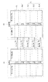
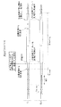
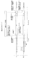
図1は、例えばC−PHY規格やD−PHY規格の通信インタフェースに対応した通信システムの概要を示している。図1に示した通信システムは、送信部TXと、受信部RXとを備えている。また、この通信システムは、送信部TXと受信部RXとに跨がって、クロック信号を伝送するクロックレーンCLと、例えば画像データ等のデータ信号を伝送するデータレーンDLとを備えている。なお、図1では、データレーンDLとして、4つのデータレーンDL1,DL2,DL3,DL4を有した例を示しているが、データレーンDLの数はこれに限らず、例えば1つのデータレーンDL1のみであってもよい。 FIG. 1 shows an outline of a communication system corresponding to, for example, a C-PHY standard or a D-PHY standard communication interface. The communication system shown in FIG. 1 includes a transmission unit TX and a reception unit RX. Further, this communication system includes a clock lane CL that transmits a clock signal across a transmission unit TX and a reception unit RX, and a data lane DL that transmits a data signal such as image data. Note that FIG. 1 shows an example in which four data lanes DL1, DL2, DL3, and DL4 are provided as the data lane DL, but the number of data lane DLs is not limited to this, for example, only one data lane DL1. It may be.
送信部TXは、送信デジタル回路TX−DIGITALと、送信アナログ回路TX−ANALOGとを有している。送信デジタル回路TX−DIGITALと送信アナログ回路TX−ANALOGとの間では、例えば16ビットや8ビットのパラレル信号が伝送される。 The transmission unit TX includes a transmission digital circuit TX-DIGITAL and a transmission analog circuit TX-ANALOG. For example, a 16-bit or 8-bit parallel signal is transmitted between the transmission digital circuit TX-DIGITAL and the transmission analog circuit TX-ANALOG.
受信部RXは、受信デジタル回路RX−DIGITALと、受信アナログ回路RX−ANALOGとを有している。データレーンDL1,DL2,DL3,DL4において、受信アナログ回路RX−ANALOGと受信デジタル回路RX−DIGITALとの間では、例えば16ビットや8ビットのパラレル信号が伝送される。クロックレーンCLにおいて、受信アナログ回路RX−ANALOGと受信デジタル回路RX−DIGITALとの間では、例えば2ビットのシリアル信号が伝送される。 The receiving unit RX has a receiving digital circuit RX-DIGITAL and a receiving analog circuit RX-ANALOG. In the data lanes DL1, DL2, DL3, DL4, for example, a 16-bit or 8-bit parallel signal is transmitted between the reception analog circuit RX-ANALOG and the reception digital circuit RX-DIGITAL. In the clock lane CL, for example, a 2-bit serial signal is transmitted between the reception analog circuit RX-ANALOG and the reception digital circuit RX-DIGITAL.
クロックレーンCLにおいて、送信アナログ回路TX−ANALOGと受信アナログ回路RX−ANALOGとの間は、差動のクロック信号を伝送するクロック信号線30で接続されている。データレーンDL1,DL2,DL3,DL4において、送信アナログ回路TX−ANALOGと受信アナログ回路RX−ANALOGとの間は、差動のデータ信号を伝送するデータ信号線31,32,33,34で接続されている。クロック信号線30とデータ信号線31,32,33,34とはそれぞれ、差動信号を伝送する一対のポジティブ信号線Dpとネガティブ信号線Dnとを有している。クロック信号線30とデータ信号線31,32,33,34とにはそれぞれ、例えば2ビットのシリアル信号が伝送される。
In the clock lane CL, the transmission analog circuit TX-ANALOG and the reception analog circuit RX-ANALOG are connected by a
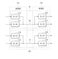
図2は、図1に示した通信システムを実現する、比較例に係る通信システムの一構成例を示している。なお、図2では、図1におけるデータレーンDLとして、1つのデータレーンDL1のみを示すが、他のデータレーンDL2,DL3,DL4についても略同様の構成であってもよい、 FIG. 2 shows a configuration example of a communication system according to a comparative example that realizes the communication system shown in FIG. In FIG. 2, only one data lane DL1 is shown as the data lane DL in FIG. 1, but the other data lanes DL2, DL3, and DL4 may have substantially the same configuration.
この比較例に係る通信システムは、図1の送信部TXに相当する送信部101と、図1の受信部RXに相当する受信部102とを備えている。
The communication system according to this comparative example includes a
クロックレーンCLにおいて、送信部101は、HS差動信号の処理を行うCL−HS回路111と、LP信号の処理を行うCL−LP回路112とを有している。データレーンDL1において、送信部101は、HS差動信号の処理を行うDL−HS回路113と、LP信号の処理を行うDL−LP回路114とを有している。
In the clock lane CL, the
クロックレーンCLにおいて、受信部102は、HS差動信号の処理を行うCL−HS回路121と、LP信号の処理を行うCL−LP回路122とを有している。データレーンDL1において、受信部102は、HS差動信号の処理を行うDL−HS回路123と、LP信号の処理を行うDL−LP回路124とを有している。
In the clock lane CL, the receiving
図3は、図2に示した比較例に係る通信システムの具体的な回路構成例を示している。また、図4は、図2に示した比較例に係る通信システムにおいてクロックレーンCLとデータレーンDL1とに伝送されるそれぞれの信号波形の一例を示している。 FIG. 3 shows a specific circuit configuration example of the communication system according to the comparative example shown in FIG. Further, FIG. 4 shows an example of each signal waveform transmitted to the clock lane CL and the data lane DL1 in the communication system according to the comparative example shown in FIG.
図4に示したように、この比較例に係る通信システムでは、クロックレーンCLにおいて、送信部101からクロック信号線30に出力される信号のステータスは、HS差動信号で伝送する状態となるHPS(High Speed State)の期間と、LP信号で伝送する状態となるLPS(Low Power State)の期間とが存在する。実質的なクロック信号は、HPSの期間にHS差動信号で出力される。
As shown in FIG. 4, in the communication system according to this comparative example, in the clock lane CL, the status of the signal output from the
同様に、データレーンDL1において、送信部101からデータ信号線31に出力される信号のステータスは、HS差動信号で伝送する状態となるHPSの期間と、LP信号で伝送する状態となるLPSの期間とが存在する。実質的なデータ信号は、HPSの期間にHS差動信号で出力される。なお、図4において、実質的なデータ信号の部分をHSTと記す。また、HPSの期間には、TRAIL期間THS-TRAILやSYNC(同期)期間THS-SYNC等が含まれる。実質的なデータ信号の部分を含まないブランキング期間は、LPSの期間に含まれる。実質的なデータ信号は、例えばByte単位で出力される。
Similarly, in the data lane DL1, the status of the signal output from the
図3に示したように、この通信システムは、送信部101内の各回路部にクロック信号を供給する水晶発振器(XTAL)82およびPLL回路81と、受信部102内の各回路部にクロック信号を供給する水晶発振器(XTAL)83とを有している。
As shown in FIG. 3, this communication system has a crystal oscillator (XTAL) 82 and a
CL−HS回路111は、HSステートマシン(HS FSM)51と、セレクタ52と、パラレル/シリアル(PS)変換回路53と、クロック分周器(DIV)54と、HSドライバ(HS DRV)55とを有している。セレクタ52は、Toggle信号と、値0の信号(ALL0)と、値1の信号(ALL1)とを選択的に出力する。Toggle信号は、例えば8ビットのクロック信号(1010_1010)である。
The CL-
CL−LP回路112は、LPステートマシン(LP FSM)41と、LPエンコーダ(LP ENC)42と、LPドライバ(LP DRV)43とを有している。LPステートマシン41には、クロックレーン制御信号が入力される。
The CL-
DL−HS回路113は、HSステートマシン(HS FSM)71と、セレクタ72と、パラレル/シリアル(PS)変換回路73と、HSドライバ(HS DRV)74とを有している。HSステートマシン71からは、データ送信準備完了信号TxReadyHSが出力される。セレクタ72は、送信データTxDataHSと、同期コード信号SYNCと、値0の信号(ALL0)と、値1の信号(ALL1)とを選択的に出力する。
The DL-
DL−LP回路114は、LPステートマシン(LP FSM)61と、LPエンコーダ(LP ENC)62と、LPドライバ(LP DRV)63とを有している。LPステートマシン61には、データ送信要求信号TxRequestHSが入力される。
The DL-
なお、送信部101において、LPドライバ43と、HSドライバ55と、LPドライバ63と、HSドライバ74は、図1における送信アナログ回路TX−ANALOGに相当する。
In the
CL−HS回路121は、クロック信号終端回路としての終端回路(TERM)56と、HSレシーバ(HS RCV)57と、クロック分周器(DIV)58とを有している。終端回路56は、終端抵抗を有している。
The CL-
CL−LP回路122は、LPレシーバ(LP RCV)44と、LPデコーダ(LP DEC)45と、LPステートマシン(LP FSM)46とを有している。LPステートマシン46は、クロックレーンCLのステータス信号を出力する。
The CL-
DL−HS回路123は、データ信号終端回路としての終端回路(TERM)75と、HSレシーバ(HS RCV)76と、クロック分周器(DIV)77と、ワードアライン補正回路(ALN)78とを有している。終端回路75は、終端抵抗を有している。ワードアライン補正回路(ALN)78は、受信同期信号RxSyncHSと、受信有効信号RxValidHSと、受信データRxDataHSとを出力する。
The DL-
DL−LP回路124は、LPレシーバ(LP RCV)64、LPデコーダ(LP DEC)65、LPステートマシン(LP FSM)66とを有している。LPステートマシン66は、受信アクティブ信号RxActiveHSを出力する。
The DL-
なお、受信部102において、主として、LPレシーバ44と、終端回路56と、HSレシーバ57と、LPレシーバ64と、終端回路75と、HSレシーバ76とが、図1における受信アナログ回路RX−ANALOGに相当する。
In the receiving
<1.第1の実施の形態>
次に、本開示の第1の実施の形態について説明する。以下では、上記比較例と略同様の構成および作用を有する部分については、適宜説明を省略する。
<1. First Embodiment>
Next, the first embodiment of the present disclosure will be described. In the following, the description of the portion having substantially the same configuration and operation as the above comparative example will be omitted as appropriate.
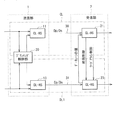
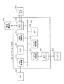
図5は、図1に示した通信システムを実現する、本開示の第1の実施の形態に係る通信システムの概要を示している。図6は、図5に示した通信システムの具体的な回路構成例を示している。なお、図5等では、図1におけるデータレーンDLとして、1つのデータレーンDL1のみを示すが、他のデータレーンDL2,DL3,DL4についても略同様の構成であってもよい。 FIG. 5 shows an outline of the communication system according to the first embodiment of the present disclosure, which realizes the communication system shown in FIG. FIG. 6 shows a specific circuit configuration example of the communication system shown in FIG. In FIG. 5 and the like, only one data lane DL1 is shown as the data lane DL in FIG. 1, but the other data lanes DL2, DL3, and DL4 may have substantially the same configuration.
本実施の形態に係る通信システムは、図1の送信部TXに相当する送信部1(送信装置)と、図1の受信部RXに相当する受信部2(受信装置)とを備えている。送信部1は、ブランキング制御部20を有している。
The communication system according to the present embodiment includes a transmitting unit 1 (transmitting device) corresponding to the transmitting unit TX of FIG. 1 and a receiving unit 2 (receiving device) corresponding to the receiving unit RX of FIG. The
図2ないし図4に示した比較例に係る通信システムでは、クロック信号およびデータ信号のブランキング期間に1.3V程度の電圧のLP信号を出力する通信モードを用いている。しかし、半導体プロセスの進化に伴って、この電圧を維持することが困難になりつつある。 The communication system according to the comparative example shown in FIGS. 2 to 4 uses a communication mode that outputs an LP signal having a voltage of about 1.3 V during the blanking period of the clock signal and the data signal. However, with the evolution of semiconductor processes, it is becoming difficult to maintain this voltage.
そこで、本実施の形態に係る通信システムでは、クロックレーンCLにおいて、送信部1からクロック信号線30に出力される信号を、ブランキング期間も含めてすべてHS差動信号のみとしている。同様に、データレーンDL1において、送信部1からデータ信号線31に出力される信号を、ブランキング期間も含めてすべてHS差動信号のみとしている。
Therefore, in the communication system according to the present embodiment, in the clock lane CL, all the signals output from the
また、本実施の形態に係る通信システムでは、ブランキング期間における通信モード(ブランキングモード)を複数有している。 Further, the communication system according to the present embodiment has a plurality of communication modes (blanking modes) during the blanking period.
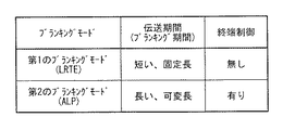
図7は、本実施の形態におけるブランキングモードの一例を示している。本実施の形態では、ブランキングモードとして、例えば、相対的に伝送期間の短い第1のブランキングモードと、相対的に伝送期間の長い第2のブランキングモードとを有している。 FIG. 7 shows an example of the blanking mode in the present embodiment. In the present embodiment, as the blanking mode, for example, a first blanking mode having a relatively short transmission period and a second blanking mode having a relatively long transmission period are provided.
第1のブランキングモードは、ブランキング間隔を極力小さくする通信(Latency Reduction Transport Efficiency:LRTE)モードである。LRTEモードでは、伝送期間は固定長となっている。また、LRTEモードでは、終端制御を行わない(終端抵抗のオン/オフの切り替えを行わない)モードとなっている。 The first blanking mode is a communication (Latency Reduction Transport Efficiency: LRTE) mode in which the blanking interval is minimized. In the LRTE mode, the transmission period is a fixed length. Further, in the LRTE mode, the terminating control is not performed (the terminating resistor is not switched on / off).
第2のブランキングモードは、長期のブランキング期間に適した(AlternateLP:ALP)モードである。ALPモードでは、伝送期間は可変長となっている。また、ALPモードでは、終端制御を行うことが可能(終端抵抗のオン/オフの切り替えが可能)なモードとなっている。 The second blanking mode is an (AlternateLP: ALP) mode suitable for a long blanking period. In the ALP mode, the transmission period has a variable length. Further, in the ALP mode, the terminating control can be performed (the terminating resistor can be switched on / off).
図8は、本実施の形態に係る通信システムで伝送されるイメージデータのフレーム構造の一例を示している。図8では、2フレーム分のイメージデータのフレーム構造を示している。フレームの先頭はFS(フレームスタート)、フレームの終わりはFE(フレームエンド)となっている。フレーム間はフレームブランキング期間(垂直ブランキング期間)Vbとなっている。1フレーム内において、1水平期間の先頭はPH(パケットヘッダ)、1水平期間の終わりはPF(パケットフッタ)となっている。 FIG. 8 shows an example of a frame structure of image data transmitted by the communication system according to the present embodiment. FIG. 8 shows the frame structure of the image data for two frames. The beginning of the frame is FS (frame start), and the end of the frame is FE (frame end). Between frames is a frame blanking period (vertical blanking period) Vb. Within one frame, the beginning of one horizontal period is PH (packet header) and the end of one horizontal period is PF (packet footer).
水平ブランキング期間Hb内には、位相差方式のオートフォーカスに用いられる位相差検出データPDAF(Phase Detection Auto-Focus)等のデータ信号が挿入されてもよい。水平ブランキング期間Hbにおいて、PDAF(Phase Detection Auto-Focus)等のデータ信号が挿入された期間Hb2を除く期間Hb1が実質的な水平ブランキング期間となる。この場合、水平ブランキング期間Hb1は非常に短期間となる。このため、本実施の形態に係る通信システムにおいて、水平ブランキング期間Hb1の通信は、ブランキングモードとして第1のブランキングモード(LRTEモード)が適している。また、垂直ブランキング期間)Vbの通信は、第2のブランキングモード(ALPモード)が適している。 Data signals such as phase difference detection data PDAF (Phase Detection Auto-Focus) used for phase difference type autofocus may be inserted in the horizontal blanking period Hb. In the horizontal blanking period Hb, the period Hb1 excluding the period Hb2 in which the data signal such as PDAF (Phase Detection Auto-Focus) is inserted is the substantial horizontal blanking period. In this case, the horizontal blanking period Hb1 is a very short period. Therefore, in the communication system according to the present embodiment, the first blanking mode (LRTE mode) is suitable as the blanking mode for the communication during the horizontal blanking period Hb1. Further, the second blanking mode (ALP mode) is suitable for the communication of the vertical blanking period) Vb.
このようにブランキング期間に複数の通信モードが混在する場合、受信部2側で複数の通信モードを判別する必要がある。判別手法の1つとしてクロック信号が止まっている期間の長さを計測する手法が考えられるが、この場合、受信部2側でカウンタを用意する必要がある。
When a plurality of communication modes coexist during the blanking period as described above, it is necessary for the receiving
そこで、本実施の形態では、カウンタを用いることなく、複数の通信モードの判別を行うことを可能にする。本実施の形態では、送信部1において、ブランキング制御部20が、通信モードに応じて、データブランキング信号とクロックブランキング信号との信号値を、例えば後述する図9および図10に示したような、通信モードを判別可能な値に制御する。また、受信部2において、後述するクロック状態判別回路59(図6)が、例えば後述する図9および図10に示したような値を参照して通信モードを判別する。
Therefore, in the present embodiment, it is possible to discriminate a plurality of communication modes without using a counter. In the present embodiment, in the
図9は、本実施の形態に係る通信システムにおいてクロックレーンCLとデータレーンDL1とに伝送されるそれぞれの信号波形の第1の例を示している。図9では、ブランキング期間における通信モードが第1のブランキングモード(LRTEモード)の例を示している。 FIG. 9 shows a first example of each signal waveform transmitted to the clock lane CL and the data lane DL1 in the communication system according to the present embodiment. FIG. 9 shows an example in which the communication mode in the blanking period is the first blanking mode (LRTE mode).
図10は、本実施の形態に係る通信システムにおいてクロックレーンCLとデータレーンDL1とに伝送されるそれぞれの信号波形の第2の例を示している。図10では、ブランキング期間における通信モードが第2のブランキングモード(ALPモード)の例を示している。 FIG. 10 shows a second example of each signal waveform transmitted to the clock lane CL and the data lane DL1 in the communication system according to the present embodiment. FIG. 10 shows an example in which the communication mode during the blanking period is the second blanking mode (ALP mode).
なお、図9および図10において、実質的なデータ信号の部分をHSTと記す。実質的なデータ信号の前後の期間にはSYNC(同期)期間THS-SYNCとTRAIL期間THS-TRAILとが含まれていてもよい。 In addition, in FIG. 9 and FIG. 10, the part of the substantial data signal is referred to as HST. The period before and after the substantial data signal may include a SYNC (synchronous) period T HS-SYNC and a TRAIL period T HS-TRAIL .
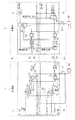
図6に示したように、本実施の形態に係る通信システムは、送信部1内の各回路部にクロック信号を供給する水晶発振器(XTAL)82およびPLL回路81と、受信部2内の各回路部にクロック信号を供給する水晶発振器(XTAL)83およびPLL回路84とを有している。
As shown in FIG. 6, the communication system according to the present embodiment includes a crystal oscillator (XTAL) 82 and a
(送信部1の詳細な構成例)
クロックレーンCLにおいて、送信部1は、HS差動信号の処理を行うCL−HS回路11を有している。データレーンDL1において、送信部1は、HS差動信号の処理を行うDL−HS回路13を有している。
(Detailed configuration example of transmitter 1)
In the clock lane CL, the
CL−HS回路11は、クロック信号およびクロックブランキング信号としてHS差動信号をクロック信号線30に出力する差動クロック信号送信回路であってもよい。DL−HS回路13は、データ信号およびデータブランキング信号としてHS差動信号をデータ信号線31に出力する差動データ信号送信回路であってもよい。
The CL-
本実施の形態における送信部1には、上記比較例におけるLP信号の処理を行うCL−LP回路112およびDL−LP回路114に相当する回路は含まれていなくともよい。
The
CL−HS回路11は、図6に示したように、図3におけるCL−HS回路111と略同様の回路を有していてもよい。すなわち、CL−HS回路11は、HSステートマシン(HS FSM)51と、セレクタ52と、パラレル/シリアル(PS)変換回路53と、クロック分周器(DIV)54と、HSドライバ(HS DRV)55とを有していてもよい。セレクタ52は、Toggle信号と、値0の信号(ALL0)と、値1の信号(ALL1)とを選択的に出力する。Toggle信号は、例えば8ビットのクロック信号(1010_1010)である。本実施の形態では、クロックレーン制御信号とデータ送信要求信号TxRequestHSとが、HSステートマシン51に入力される。
As shown in FIG. 6, the CL-
DL−HS回路13は、図6に示したように、図3におけるDL−HS回路113と略同様の回路を有していてもよい。すなわち、DL−HS回路13は、HSステートマシン(HS FSM)71と、セレクタ72と、パラレル/シリアル(PS)変換回路73と、HSドライバ(HS DRV)74とを有していてもよい。HSステートマシン71からは、データ送信準備完了信号TxReadyHSが出力される。セレクタ72は、送信データTxDataHSと、同期コード信号SYNCと、値0の信号(ALL0)と、値1の信号(ALL1)とを選択的に出力する。
As shown in FIG. 6, the DL-
ブランキング制御部20は、図6に示したように、HSステートマシン51とHSステートマシン71とを有していてもよい。
As shown in FIG. 6, the blanking
(送信部1におけるモード制御動作の例)
図9の第1のブランキングモードによる通信を行う場合、ブランキング制御部20は、データ信号のブランキング期間の開始時刻に同期して、DL−HS回路13からデータ信号線31に、データ信号に代えて、例えば値1のデータブランキング信号が出力されるよう、DL−HS回路13を制御する。
(Example of mode control operation in transmitter 1)
When communicating in the first blanking mode of FIG. 9, the blanking
また、第1のブランキングモードによる通信を行う場合、ブランキング制御部20は、データ信号のブランキング期間の開始時刻に同期して、CL−HS回路11からクロック信号線30に、クロック信号に代えて所定の期間以上に亘って、例えば値0のクロックブランキング信号が連続する差動ブランキング信号が出力されるよう、CL−HS回路11を制御する。ここで、所定の期間とは、クロック信号のクロック周期よりも長い期間である。クロックブランキング信号を、クロック信号のクロック周期よりも長い期間に亘って値0の信号値が連続する信号とすることで、受信部2のクロック状態判別回路59において、信号の変化を検出することができ、ブランキング期間が開始されたことを検出することが可能となる。
Further, when communicating in the first blanking mode, the blanking
また、第1のブランキングモードによる通信を行う場合、ブランキング制御部20は、データ信号のブランキング期間の終了時刻に同期して、CL−HS回路11からクロック信号線30に、クロックブランキング信号に代えて、所定の期間以上に亘ってクロック信号が出力されるよう、CL−HS回路11を制御する。クロックブランキング信号に代えて所定の期間以上に亘るクロック信号を出力することで、受信部2のクロック状態判別回路59において、信号の変化を検出することができ、ブランキング期間が終了し、データ信号の転送が開始されることを検出することが可能となる。
Further, when performing communication in the first blanking mode, the blanking
一方、図10の第2のブランキングモードによる通信を行う場合、ブランキング制御部20は、データ信号のブランキング期間の開始時刻に同期して、DL−HS回路13からデータ信号線31に、データ信号に代えて、値0のデータブランキング信号が出力されるよう、DL−HS回路13を制御する。
On the other hand, when communicating in the second blanking mode of FIG. 10, the blanking
また、第2のブランキングモードによる通信を行う場合、ブランキング制御部20は、データ信号のブランキング期間の開始時刻に同期して、CL−HS回路11からクロック信号線30に、クロック信号に代えて所定の期間以上に亘って、例えば値0のクロックブランキング信号が連続する差動ブランキング信号が出力されるよう、CL−HS回路11を制御する。ここで、所定の期間とは、クロック信号のクロック周期よりも長い期間である。クロックブランキング信号を、クロック信号のクロック周期よりも長い期間に亘って値0の信号値が連続する信号とすることで、受信部2のクロック状態判別回路59において、信号の変化を検出することができ、ブランキング期間が開始されたことを検出することが可能となる。
Further, when performing communication in the second blanking mode, the blanking
また、第2のブランキングモードによる通信を行う場合、ブランキング制御部20は、データ信号のブランキング期間の終了時刻に同期して、CL−HS回路11からクロック信号線30に、値0のクロックブランキング信号に代えて、所定の期間以上に亘って、例えば値1のクロックブランキング信号が出力されるよう、CL−HS回路11を制御する。値0のクロックブランキング信号に代えて所定の期間以上に亘る値1のクロックブランキング信号を出力することで、受信部2のクロック状態判別回路59において、信号の変化を検出することができ、ブランキング期間が終了し、データ信号の転送が開始されることを検出することが可能となる。
Further, when performing communication in the second blanking mode, the blanking
図9および図10に示した例のように、データ信号のブランキング期間の開始時のデータブランキング信号の値を、第1のブランキングモードと第2のブランキングモードとで異なる値とすることで、受信部2のクロック状態判別回路59において、通信モードを判別することが可能となる。
As in the example shown in FIGS. 9 and 10, the value of the data blanking signal at the start of the blanking period of the data signal is set to a different value between the first blanking mode and the second blanking mode. This makes it possible for the clock
なお、図9および図10に示したクロックブランキング信号およびデータブランキング信号の値は一例であり、図9および図10の例とは異なる値を用いても構わない。 The values of the clock blanking signal and the data blanking signal shown in FIGS. 9 and 10 are examples, and values different from the examples of FIGS. 9 and 10 may be used.
なお、図11に、差動信号の値の一例を示す。値0のクロックブランキング信号およびデータブランキング信号は、差動0(Differential-0)となる差動信号であってもよい。また、値1のクロックブランキング信号およびデータブランキング信号は、差動1(Differential-1)となる差動信号であってもよい。より具体的には、図11に示したように、値0の差動信号は、差動信号の伝送線におけるポジティブ信号線Dpの電圧レベルがLowとなり、ネガティブ信号線Dnの電圧レベルがHighとなる差動信号のことであってもよい。また、値1の差動信号は、差動信号の伝送線におけるポジティブ信号線Dpの電圧レベルがHighとなり、ネガティブ信号線Dnの電圧レベルがLowとなる差動信号のことであってもよい。 Note that FIG. 11 shows an example of the value of the differential signal. The clock blanking signal and the data blanking signal having a value of 0 may be differential signals having a differential of 0 (Differential-0). Further, the clock blanking signal and the data blanking signal having a value of 1 may be differential signals having a differential of 1 (Differential-1). More specifically, as shown in FIG. 11, for the differential signal having a value of 0, the voltage level of the positive signal line Dp in the transmission line of the differential signal is Low, and the voltage level of the negative signal line Dn is High. It may be a differential signal. Further, the differential signal having a value of 1 may be a differential signal in which the voltage level of the positive signal line Dp in the transmission line of the differential signal is High and the voltage level of the negative signal line Dn is Low.
(受信部2の詳細な構成例)
クロックレーンCLにおいて、受信部2は、HS差動信号の処理を行うCL−HS回路21を有している。データレーンDL1において、受信部2は、HS差動信号の処理を行うDL−HS回路23を有している。
(Detailed configuration example of receiver 2)
In the clock lane CL, the receiving
DL−HS回路23は、データ信号およびデータブランキング信号としてHS差動信号をデータ信号線31を介して受信する差動データ信号受信回路であってもよい。CL−HS回路21は、クロック信号およびクロックブランキング信号としてHS差動信号をクロック信号線30を介して受信する差動クロック信号受信回路であってもよい。
The DL-
本実施の形態における受信部2には、上記比較例におけるLP信号の処理を行うCL−LP回路122およびDL−LP回路124に相当する回路は含まれていなくともよい。
The receiving
DL−HS回路23は、図6に示したように、図3におけるDL−HS回路123と略同様の回路を有していてもよい。すなわち、データ信号線31に接続されたデータ信号終端回路としての終端回路(TERM)75と、HSレシーバ(HS RCV)76と、クロック分周器(DIV)77と、ワードアライン補正回路(ALN)78とを有していてもよい。終端回路75は、終端抵抗を有している。ワードアライン補正回路(ALN)78は、受信同期信号RxSyncHSと、受信有効信号RxValidHSと、受信データRxDataHSとを出力する。
As shown in FIG. 6, the DL-
CL−HS回路21は、図6に示したように、図3におけるCL−HS回路121と略同様の回路を有していてもよい。すなわち、CL−HS回路21は、クロック信号線30に接続されたクロック信号終端回路としての終端回路(TERM)56と、HSレシーバ(HS RCV)57と、クロック分周器(DIV)58とを有していてもよい。終端回路56は、終端抵抗を有している。
As shown in FIG. 6, the CL-
CL−HS回路21は、さらに、クロック(CL)状態判別回路59を有している。クロック状態判別回路59には、HSレシーバ57を介して送信部1のCL−HS回路11からのクロック信号とクロックブランキング信号とが入力される。また、クロック状態判別回路59には、HSレシーバ76を介して送信部1のDL−HS回路13からのデータブランキング信号が入力される。
The CL-
(受信部2におけるモード判別の例)
クロック状態判別回路59は、例えば、データ信号のブランキング期間の開始時のデータブランキング信号の値を参照することで、ブランキングモードの判別を行う。クロック状態判別回路59は、例えば図9の例のようにデータブランキング信号の値が1の場合には、第1のブランキングモードであると判別する。また、クロック状態判別回路59は、例えば図10の例のようにデータブランキング信号の値が0の場合には、第2のブランキングモードであると判別する。
(Example of mode determination in receiver 2)
The clock
(受信部2における終端制御およびワードアライン制御の例)
図10の例のように第2のブランキングモードの場合、受信部2は終端制御の処理を行ってもよい。クロック状態判別回路59は、終端制御回路としての機能を有している。クロック状態判別回路59は、例えば値0のクロックブランキング信号に基づいて、データ信号終端回路(終端回路75)およびクロック信号終端回路(終端回路56)に対してそれぞれの終端抵抗をオフさせる制御を行う。また、クロック状態判別回路59は、データ信号のブランキング期間の終了時刻に同期して出力された、値1のクロックブランキング信号に基づいて、終端回路75および終端回路56に対してそれぞれの終端抵抗をオンさせる制御を行う。
(Example of termination control and word-aligned control in receiver 2)
In the case of the second blanking mode as in the example of FIG. 10, the receiving
なお、終端抵抗のオン/オフに伴い、図10に示したように、クロックレーンCLおよびデータレーンDL1のブランキング期間における信号の電圧振幅が変化する。また、ブランキング期間において終端抵抗をオフさせることにより、クロック信号線30およびデータ信号線31に流れる電流値を低減することができる。
As shown in FIG. 10, the voltage amplitude of the signal in the blanking period of the clock lane CL and the data lane DL1 changes as the terminating resistor is turned on / off. Further, by turning off the terminating resistor during the blanking period, the current value flowing through the
また、クロック状態判別回路59は、受信アクティブ信号RxActiveHSを出力しワードアライン補正回路78に対して、ワードアライン制御を行う機能を有している。ブランキング期間が終了し、データ信号の転送が開始されることをクロック状態判別回路59において適切に検出することで、同期コード信号SYNCを検出し、ワードアライン補正回路78で適切にワードアライン制御を行うことができる。
Further, the clock
[効果]
以上のように、本実施の形態によれば、データ信号のブランキング期間の開始時刻に同期して、クロック信号線30に、クロック信号に代えて、クロックブランキング信号として、所定の期間以上に亘って所定の値が連続する差動ブランキング信号を出力するようにしたので、データ伝送時の低消費電力化を図ることができる。また、本実施の形態によれば、上記した比較列に係る通信システムと比べて、LP信号の処理を行う回路が不要となり、回路規模を削減することができる。
[effect]
As described above, according to the present embodiment, in synchronization with the start time of the blanking period of the data signal, the
また、本実施の形態によれば、送信部1側でデータブランキング信号の信号値をブランキングモードを判別可能な値に制御し、受信部2側でデータブランキング信号の信号値に基づいてブランキングモードを判別するようにしたので、受信部2側でブランキングモードを判別するためのカウンタを用いることなく、複数のブランキングモードの判別を容易に行うことができる。
Further, according to the present embodiment, the signal value of the data blanking signal is controlled on the transmitting
なお、本明細書に記載された効果はあくまでも例示であって限定されるものではなく、また他の効果があってもよい。以降の他の実施の形態の効果についても同様である。 It should be noted that the effects described in the present specification are merely examples and are not limited, and other effects may be obtained. The same applies to the effects of the other embodiments thereafter.
<2.第2の実施の形態>
次に、本開示の第2の実施の形態について説明する。以下では、上記比較例、または上記第1の実施の形態と略同様の構成および作用を有する部分については、適宜説明を省略する。
<2. Second Embodiment>
Next, a second embodiment of the present disclosure will be described. In the following, description of the comparative example or a portion having substantially the same configuration and operation as that of the first embodiment will be omitted as appropriate.
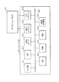
図12は、本開示の第2の実施の形態に係る通信システムの概要を示している。本実施の形態に係る通信システムは、図1の送信部TXに相当する送信部1B(送信装置)と、図1の受信部RXに相当する受信部2B(受信装置)とを備えている。 FIG. 12 shows an outline of the communication system according to the second embodiment of the present disclosure. The communication system according to the present embodiment includes a transmitting unit 1B (transmitting device) corresponding to the transmitting unit TX of FIG. 1 and a receiving unit 2B (receiving device) corresponding to the receiving unit RX of FIG.
上記第1の実施の形態に係る通信システムでは、クロックレーンCLとデータレーンDL1とのそれぞれにおいて伝送される信号を、ブランキング期間も含めてすべてHS差動信号のみにしている。これに対して、本実施の形態に係る通信システムは、LP信号での通信も可能にする切り替え回路を備え、LP信号を用いずにHS差動信号のみで通信を行うモードと、LP信号とHS差動信号との双方を用いて通信を行うモードとを切り替え可能にしたものである。 In the communication system according to the first embodiment, the signals transmitted in each of the clock lane CL and the data lane DL1 are all HS differential signals including the blanking period. On the other hand, the communication system according to the present embodiment includes a switching circuit that enables communication with LP signals, and has a mode in which communication is performed only with HS differential signals without using LP signals, and LP signals. It is possible to switch between the mode in which communication is performed using both the HS differential signal and the HS differential signal.
本実施の形態に係る通信システムにおいて、送信部1Bは、上記第1の実施の形態に係る通信システムと略同様の機能を実現するブランキング制御部20を有している。
In the communication system according to the present embodiment, the transmission unit 1B has a blanking
また、送信部1Bは、クロックレーンCLにおいて、HS差動信号の処理を行うCL−HS回路11と、LP信号の処理を行うCL−LP回路12と、切り替えスイッチ15と、セレクタ17とを有している。
Further, the transmission unit 1B has a CL-
CL−LP回路12は、LP信号として第1のシングルエンド信号を出力する第1のシングルエンド信号送信回路であってもよい。CL−LP回路12は、図2におけるCL−LP回路112と略同様の機能を有するものであってもよい。切り替えスイッチ15は、クロック信号線30に、CL−HS回路11とCL−LP回路12とのいずれか一方から信号出力がなされるよう、信号出力の経路を切り替える第1の送信切り替え回路であってもよい。セレクタ17は、LP信号を用いずにHS差動信号のみで通信を行うモードではブランキング制御部20からの制御信号がCL−HS回路11に入力されるようにし、LP信号とHS差動信号との双方を用いて通信を行うモードでは、ブランキング制御部20からの制御信号がCL−HS回路11に入力されないようにする回路である。
The CL-
また、送信部1Bは、データレーンDL1において、HS差動信号の処理を行うDL−HS回路13と、LP信号の処理を行うDL−LP回路14と、切り替えスイッチ16と、セレクタ18とを有している。
Further, the transmission unit 1B has a DL-
DL−LP回路14は、LP信号として第2のシングルエンド信号を出力する第2のシングルエンド信号送信回路であってもよい。DL−LP回路14は、図2におけるDL−LP回路114と略同様の機能を有するものであってもよい。切り替えスイッチ16は、データ信号線31にDL−HS回路13とDL−LP回路14とのいずれか一方から信号出力がなされるよう、信号出力の経路を切り替える第2の送信切り替え回路であってもよい。セレクタ18は、LP信号を用いずにHS差動信号のみで通信を行うモードではブランキング制御部20からの制御信号がDL−HS回路13に入力されるようにし、LP信号とHS差動信号との双方を用いて通信を行うモードでは、ブランキング制御部20からの制御信号がDL−HS回路13に入力されないようにする回路である。
The DL-
受信部2Bは、クロックレーンCLにおいて、HS差動信号の処理を行うCL−HS回路21と、LP信号の処理を行うCL−LP回路22と、セレクタ25と、セレクタ27と、セレクタ28とを有している。CL−LP回路22は、LP信号として第1のシングルエンド信号をクロック信号線30を介して受信する第1のシングルエンド信号受信回路であってもよい。CL−LP回路22は、図2におけるCL−LP回路122と略同様の機能を有するものであってもよい。
In the clock lane CL, the receiving unit 2B includes a CL-
セレクタ25は、LP信号として第1のシングルエンド信号を受信するか否かを切り替える第1の受信切り替え回路であってもよい。セレクタ25は、LP信号を用いずにHS差動信号のみで通信を行うモードではクロック信号線30を介して受信した信号がCL−LP回路22に入力されないようにし、LP信号とHS差動信号との双方を用いて通信を行うモードでは、クロック信号線30を介して受信した信号がCL−LP回路22に入力されるようにする回路である。セレクタ27は、LP信号を用いずにHS差動信号のみで通信を行うモードではCL−HS回路21からの終端制御の信号がDL−HS回路23に入力されるようにし、LP信号とHS差動信号との双方を用いて通信を行うモードでは、HS回路21からの終端制御の信号が入力されないようにする回路である。セレクタ28は、LP信号を用いずにHS差動信号のみで通信を行うモードではCL−HS回路21からのワードアライン制御の信号がDL−HS回路23に入力されるようにし、LP信号とHS差動信号との双方を用いて通信を行うモードでは、CL−HS回路21からのワードアライン制御の信号が入力されないようにする回路である。
The
また、受信部2Bは、データレーンDL1において、HS差動信号の処理を行うDL−HS回路23と、LP信号の処理を行うDL−LP回路24と、セレクタ26とを有している。DL−LP回路24は、LP信号として第2のシングルエンド信号をデータ信号線31を介して受信する第2のシングルエンド信号受信回路であってもよい。
Further, the receiving unit 2B has a DL-
セレクタ26は、LP信号として第2のシングルエンド信号を受信するか否かを切り替える第2の受信切り替え回路であってもよい。セレクタ26は、LP信号を用いずにHS差動信号のみで通信を行うモードではデータ信号線31を介して受信した信号がDL−LP回路24に入力されないようにし、LP信号とHS差動信号との双方を用いて通信を行うモードでは、データ信号線31を介して受信した信号がDL−LP回路24に入力されるようにする回路である。
The
図13は、本実施の形態に係る通信システムの具体的な適用例を示している。 FIG. 13 shows a specific application example of the communication system according to the present embodiment.
例えば、本実施の形態に係る通信システムは、図13に示したように、イメージセンサISからアプリケーションプロセッサAPへのデータ伝送に適用可能である。送信部1Bは、イメージセンサIS内に設けられる。受信部2Bは、アプリケーションプロセッサAP内に設けられる。イメージセンサISとアプリケーションプロセッサAPとの間は、クロック信号線30とデータ信号線31とによって接続される。クロック信号線30とデータ信号線31とによる信号の伝送は一方向となっている。
For example, the communication system according to the present embodiment can be applied to data transmission from the image sensor IS to the application processor AP, as shown in FIG. The transmission unit 1B is provided in the image sensor IS. The receiving unit 2B is provided in the application processor AP. The image sensor IS and the application processor AP are connected by a
また、イメージセンサISとアプリケーションプロセッサAPとの間は、双方向の制御バス35によって接続される。制御バス35は、I2C(Inter-Integrated Circuit)インタフェースやその拡張版であるI3Cインタフェースを用いることができる。
Further, the image sensor IS and the application processor AP are connected by a
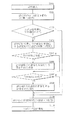
図14は、図13に示したイメージセンサISおよびアプリケーションプロセッサAPを含む機器におけるデータ送信処理の一例を示している。 FIG. 14 shows an example of data transmission processing in the device including the image sensor IS and the application processor AP shown in FIG.
イメージセンサISおよびアプリケーションプロセッサAPを含む機器の電源投入がなされる(ステップS101)と、アプリケーションプロセッサAPが、制御バス35を使用して、イメージセンサISのレジスタ設定を読み込む(ステップS102)。これにより、アプリケーションプロセッサAPは、イメージセンサISがLP信号無しでの通信に対応しているか否かを判断する(ステップS103)。すなわち、LP信号を用いずにHS差動信号のみで通信を行うモードと、LP信号とHS差動信号との双方を用いて通信を行うモードとのいずれのモードに対応しているかを判断する。 When the power of the device including the image sensor IS and the application processor AP is turned on (step S101), the application processor AP reads the register setting of the image sensor IS using the control bus 35 (step S102). As a result, the application processor AP determines whether or not the image sensor IS supports communication without the LP signal (step S103). That is, it is determined which mode corresponds to the mode in which communication is performed using only the HS differential signal without using the LP signal and the mode in which communication is performed using both the LP signal and the HS differential signal. ..
LP信号無しでの通信に対応していないと判断した場合(ステップS103;N)には、アプリケーションプロセッサAPは、LP信号とHS差動信号との双方を用いて通信を行うモードとみなして、制御バス35を使用して、イメージセンサISに送信開始指示の信号を出力する(ステップS109)。次に、イメージセンサISは、送信開始指示の信号を受けて、データ信号の送信を開始する(ステップS110)。
When it is determined that the communication without the LP signal is not supported (step S103; N), the application processor AP considers it as a mode in which communication is performed using both the LP signal and the HS differential signal. The
一方、LP信号無しでの通信に対応していると判断した場合(ステップS103;Y)には、アプリケーションプロセッサAPは、制御バス35を使用して、LP信号無しでの通信を有効化する設定をイメージセンサISに送信する(ステップS104)。
On the other hand, when it is determined that the communication without the LP signal is supported (step S103; Y), the application processor AP is set to enable the communication without the LP signal by using the
次に、アプリケーションプロセッサAPは、イメージセンサISのレジスタ設定を参照して、イメージセンサISが第1のブランキングモード(LRTEモード)での通信に対応しているか否かを判断する(ステップS105)。第1のブランキングモードでの通信に対応していないと判断した場合(ステップS105;N)には、後述するステップS107の処理に進む。第1のブランキングモードでの通信に対応していると判断した場合(ステップS105;Y)には、アプリケーションプロセッサAPは、制御バス35を使用して、第1のブランキングモードでの通信を有効化する設定をイメージセンサISに送信する(ステップS106)。
Next, the application processor AP refers to the register setting of the image sensor IS and determines whether or not the image sensor IS supports communication in the first blanking mode (LRTE mode) (step S105). .. If it is determined that the communication in the first blanking mode is not supported (step S105; N), the process proceeds to step S107 described later. When it is determined that the communication in the first blanking mode is supported (step S105; Y), the application processor AP uses the
次に、アプリケーションプロセッサAPは、イメージセンサISのレジスタ設定を参照して、イメージセンサISが第2のブランキングモード(ALPモード)での通信に対応しているか否かを判断する(ステップS107)。第2のブランキングモードでの通信に対応していないと判断した場合(ステップS107;N)には、アプリケーションプロセッサAPは、制御バス35を使用して、イメージセンサISに送信開始指示の信号を出力する(ステップS109)。次に、イメージセンサISは、送信開始指示の信号を受けて、データ信号の送信を開始する(ステップS110)。
Next, the application processor AP refers to the register setting of the image sensor IS and determines whether or not the image sensor IS supports communication in the second blanking mode (ALP mode) (step S107). .. When it is determined that the communication in the second blanking mode is not supported (step S107; N), the application processor AP uses the
一方、第2のブランキングモードでの通信に対応していると判断した場合(ステップS107;Y)には、アプリケーションプロセッサAPは、制御バス35を使用して、第2のブランキングモードでの通信を有効化する設定をイメージセンサISに送信する(ステップS108)。次に、アプリケーションプロセッサAPは、制御バス35を使用して、イメージセンサISに送信開始指示の信号を出力する(ステップS109)。次に、イメージセンサISは、送信開始指示の信号を受けて、データ信号の送信を開始する(ステップS110)。
On the other hand, when it is determined that the communication in the second blanking mode is supported (step S107; Y), the application processor AP uses the
<3.第3の実施の形態>
次に、本開示の第3の実施の形態について説明する。以下では、上記比較例、上記第1の実施の形態または上記第2の実施の形態と略同様の構成および作用を有する部分については、適宜説明を省略する。
<3. Third Embodiment>
Next, a third embodiment of the present disclosure will be described. In the following, description of the comparative example, the first embodiment, or the portion having substantially the same configuration and operation as that of the second embodiment will be omitted as appropriate.
上記第1および第2の実施の形態では、通信モードの判別として、ブランキングモードの判別を行う例を述べたが、同様の判別手法によりデータ信号の通信モード(データ伝送モード)を判別することも可能である。 In the first and second embodiments described above, an example of determining the blanking mode is described as the determination of the communication mode, but the communication mode (data transmission mode) of the data signal is determined by the same determination method. Is also possible.
図15は、本実施の形態において判別するデータ伝送モードの一例を示している。本実施の形態では、データ伝送モードとして、例えば、相対的に伝送速度が高速な第1のデータ伝送モード(高速伝送モード)と、相対的に伝送速度が低速な第2のデータ伝送モード(低速伝送モード)とを判別する。高速伝送モードと低速伝送モードは共に差動信号の伝送を行うモードであり、例えば電圧振幅を変えることにより伝送速度が互いに異なる。 FIG. 15 shows an example of the data transmission mode to be discriminated in the present embodiment. In the present embodiment, as the data transmission modes, for example, a first data transmission mode (high-speed transmission mode) having a relatively high transmission speed and a second data transmission mode (low speed transmission mode) having a relatively low transmission speed. (Transmission mode) is determined. Both the high-speed transmission mode and the low-speed transmission mode are modes in which differential signals are transmitted. For example, the transmission speeds differ from each other by changing the voltage amplitude.
なお、本実施の形態における通信システムの基本構成は、図5および図6の構成と略同様であってもよい。送信部1において、ブランキング制御部20は、通信モードに応じて、データブランキング信号とクロックブランキング信号との信号値を、例えば後述する図17、図19、および図21に示したような、通信モードを判別可能な値に制御する。また、受信部2において、クロック状態判別回路59は、例えば後述する図17、図19、および図21に示したような値を参照して通信モードを判別する。
The basic configuration of the communication system in the present embodiment may be substantially the same as the configurations of FIGS. 5 and 6. In the
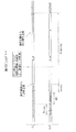
(データ伝送モードの判別方法の第1の例)
図16は、本実施の形態に係る通信システムにおいてクロックレーンCLとデータレーンDL1とに伝送されるそれぞれの信号波形の第1の例を示している。図16では、図9の例と同様、ブランキング期間における通信モードが第1のブランキングモード(LRTEモード)の例を示している。図17は、ブランキング期間における通信モードが第1のブランキングモードである場合におけるデータ信号の通信モードの判別方法の一例を示している。
(First example of data transmission mode determination method)
FIG. 16 shows a first example of each signal waveform transmitted to the clock lane CL and the data lane DL1 in the communication system according to the present embodiment. FIG. 16 shows an example in which the communication mode during the blanking period is the first blanking mode (LRTE mode), as in the example of FIG. FIG. 17 shows an example of a method of determining the communication mode of the data signal when the communication mode in the blanking period is the first blanking mode.
ブランキング制御部20は、データ信号のブランキング期間の開始時刻に同期して、DL−HS回路13からデータ信号線31に、データ信号に代えて、値Dnt0のデータブランキング信号が出力されるよう、DL−HS回路13を制御する。
The blanking
また、ブランキング制御部20は、データ信号のブランキング期間の開始時刻に同期して、CL−HS回路11からクロック信号線30に、クロック信号に代えて所定の期間以上に亘って値Cnt0のクロックブランキング信号が連続する差動ブランキング信号が出力されるよう、CL−HS回路11を制御する。ここで、所定の期間とは、クロック信号のクロック周期よりも長い期間である。クロックブランキング信号を、クロック信号のクロック周期よりも長い期間に亘って値Cnt0の信号値が連続する信号とすることで、受信部2のクロック状態判別回路59において、信号の変化を検出することができ、ブランキング期間が開始されたことを検出することが可能となる。
Further, blanking
また、ブランキング制御部20は、データ信号のブランキング期間の終了時刻に同期して、CL−HS回路11からクロック信号線30に、クロックブランキング信号に代えて、所定の期間以上に亘ってクロック信号が出力されるよう、CL−HS回路11を制御する。クロックブランキング信号に代えて所定の期間以上に亘るクロック信号を出力することで、受信部2のクロック状態判別回路59において、信号の変化を検出することができ、ブランキング期間が終了し、データ信号の転送が開始されることを検出することが可能となる。
Further, the blanking
受信部2において、クロック状態判別回路59は、例えば図17に示したような値を参照して通信モードを判別する。
In the receiving
クロック状態判別回路59は、例えば、(Cnt0=0,Dnt0=0)の場合は高速伝送モード、(Cnt0=1,Dnt0=1)の場合は低速伝送モードであると判別する。また、クロック状態判別回路59は、例えば、(Cnt0=0,Dnt0=1)の場合はブランキング期間における通信モードが第1のブランキングモード(LRTEモード)であると判別する。なお、(Cnt0=1,Dnt0=0)は、例えば将来的にその他の通信モードの判別に利用可能な予備の値(「Reserved」)とする。
The clock
なお、図17に示した値と通信モードとの組み合わせは一例であり、図17とは異なる組み合わせであっても構わない。また、3種類以上のデータ伝送モードの判別を行ってもよい。 The combination of the value shown in FIG. 17 and the communication mode is an example, and may be a combination different from that shown in FIG. Further, three or more types of data transmission modes may be discriminated.
(データ伝送モードの判別方法の第2の例)
図18は、本実施の形態に係る通信システムにおいてクロックレーンCLとデータレーンDL1とに伝送されるそれぞれの信号波形の第2の例を示している。図18では、図10の例と同様、ブランキング期間における通信モードが第2のブランキングモード(ALPモード)の例を示している。図19は、ブランキング期間における通信モードが第2のブランキングモードである場合におけるデータ信号の通信モードの判別方法の一例を示している。
(Second example of data transmission mode determination method)
FIG. 18 shows a second example of each signal waveform transmitted to the clock lane CL and the data lane DL1 in the communication system according to the present embodiment. FIG. 18 shows an example in which the communication mode during the blanking period is the second blanking mode (ALP mode), as in the example of FIG. FIG. 19 shows an example of a method of determining the communication mode of the data signal when the communication mode in the blanking period is the second blanking mode.
ブランキング制御部20は、データ信号のブランキング期間の開始時刻に同期して、DL−HS回路13からデータ信号線31に、データ信号に代えて、値D0のデータブランキング信号が出力されるよう、DL−HS回路13を制御する。また、ブランキング制御部20は、ブランキング期間の終了時刻に同期して、DL−HS回路13からデータ信号線31に、値D0のデータブランキング信号に代えて、値D1のデータブランキング信号が出力されるよう、DL−HS回路13を制御する。
The blanking
また、ブランキング制御部20は、データ信号のブランキング期間の開始時刻に同期して、CL−HS回路11からクロック信号線30に、クロック信号に代えて所定の期間以上に亘って値C0のクロックブランキング信号が連続する差動ブランキング信号が出力されるよう、CL−HS回路11を制御する。ここで、所定の期間とは、クロック信号のクロック周期よりも長い期間である。クロックブランキング信号を、クロック信号のクロック周期よりも長い期間に亘って値C0の信号値が連続する信号とすることで、受信部2のクロック状態判別回路59において、信号の変化を検出することができ、ブランキング期間が開始されたことを検出することが可能となる。
Further, the blanking
また、ブランキング制御部20は、データ信号のブランキング期間の終了時刻に同期して、CL−HS回路11からクロック信号線30に、値C0のクロックブランキング信号に代えて、所定の期間以上に亘って値C1のクロックブランキング信号が出力されるよう、CL−HS回路11を制御する。値C0のクロックブランキング信号に代えて所定の期間以上に亘る値C1のクロックブランキング信号を出力することで、受信部2のクロック状態判別回路59において、信号の変化を検出することができ、ブランキング期間が終了し、データ信号の転送が開始されることを検出することが可能となる。
Further, the blanking
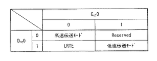
受信部2において、クロック状態判別回路59は、例えば図19に示したような値を参照して通信モードを判別する。
In the receiving
クロック状態判別回路59は、例えば、(C0=0,C1=1)かつ(D0=0,D1=0)の場合は高速伝送モードであると判別する。また、クロック状態判別回路59は、例えば、(C0=0,C1=1)かつ(D0=0,D1=1)の場合は低速伝送モードであると判別する。なお、その他の値は、例えば将来的にその他の通信モードの判別に利用可能な予備の値(「Reserved」)とする。ただし、終端制御を行うためには、クロックブランキング信号の値(C0,C1)およびデータブランキング信号の値(D0,D1)のうち、少なくとも一方の値をブランキング期間内で切り替える必要がある。このため、終端制御を行う場合には、(C0=0,C1=0)かつ(D0=0,D1=0)と、(C0=0,C1=0)かつ(D0=1,D1=1)と、(C0=1,C1=1)かつ(D0=0,D1=0)と、(C0=1,C1=1)かつ(D0=1,D1=1)は、通信モードの判別には使用しない。
For example, when (C0 = 0, C1 = 1) and (D0 = 0, D1 = 0), the clock
なお、図19に示した値と通信モードとの組み合わせは一例であり、図19とは異なる組み合わせであっても構わない。また、3種類以上のデータ伝送モードの判別を行ってもよい。 The combination of the value shown in FIG. 19 and the communication mode is an example, and may be a combination different from that in FIG. Further, three or more types of data transmission modes may be discriminated.
(データ伝送モードの判別方法の第3の例)
図20は、本実施の形態に係る通信システムにおいてクロックレーンCLとデータレーンDL1とに伝送されるそれぞれの信号波形の第3の例を示している。図21は、図20に示した第3の例における通信モードの判別方法の一例を示している。
(Third example of the data transmission mode determination method)
FIG. 20 shows a third example of each signal waveform transmitted to the clock lane CL and the data lane DL1 in the communication system according to the present embodiment. FIG. 21 shows an example of a communication mode determination method in the third example shown in FIG.
図20では、通信モードが、高速伝送モード→LRTEモード→低速伝送モード→高速伝送モードの順に遷移する例を示している。 FIG. 20 shows an example in which the communication mode changes in the order of high-speed transmission mode → LRTE mode → low-speed transmission mode → high-speed transmission mode.
受信部2において、クロック状態判別回路59は、上記第2の例と同様に、例えば図21に示したようなクロックレーンCLの値(C0,C1)とデータレーンDL1の値(D0,D1)とを参照して通信モードを判別する。なお、図21には、モード遷移時の終端抵抗のオン/オフ状態の例も示す。
In the receiving
クロック状態判別回路59は、例えば、(C0=0,C1=1)かつ(D0=0,D1=0)の場合は高速伝送モードに遷移すると判別する。また、クロック状態判別回路59は、例えば、(C0=0,C1=0)かつ(D0=1,D1=1)の場合はLRTEモードに遷移すると判別する。また、クロック状態判別回路59は、例えば、(C0=0,C1=1)かつ(D0=0,D1=1)の場合は低速伝送モードに遷移すると判別する。なお、その他の値は、例えば将来的にその他の通信モードの判別に利用可能な予備の値(「Reserved」)とする。
The clock
なお、図21に示した値と通信モードとの組み合わせは一例であり、図21とは異なる組み合わせであっても構わない。 The combination of the value shown in FIG. 21 and the communication mode is an example, and may be a combination different from that in FIG.
<4.適用例>
次に、上記各実施の形態で説明した通信システムの適用例について説明する。
<4. Application example>
Next, an application example of the communication system described in each of the above embodiments will be described.
[4.1 第1の適用例]
図22は、上記各実施の形態の通信システムが適用されるスマートフォン300(多機能携帯電話)の外観を表すものである。このスマートフォン300には、様々なデバイスが搭載されており、それらのデバイス間でデータのやり取りを行う通信システムにおいて、上記各実施の形態の通信システムが適用されている。
[4.1 First application example]
FIG. 22 shows the appearance of a smartphone 300 (multifunctional mobile phone) to which the communication system of each of the above embodiments is applied. Various devices are mounted on the smartphone 300, and the communication systems of the above embodiments are applied to the communication system for exchanging data between these devices.
図23は、スマートフォン300に用いられるアプリケーションプロセッサ310の一構成例を表すものである。アプリケーションプロセッサ310は、CPU(Central Processing Unit)311と、メモリ制御部312と、電源制御部313と、外部インタフェース314と、GPU(Graphics Processing Unit)315と、メディア処理部316と、ディスプレイ制御部317と、MIPIインタフェース318とを有している。CPU311、メモリ制御部312、電源制御部313、外部インタフェース314、GPU315、メディア処理部316、ディスプレイ制御部317は、この例では、システムバス319に接続され、このシステムバス319を介して、互いにデータのやり取りをすることができるようになっている。
FIG. 23 shows a configuration example of the
CPU311は、プログラムに従って、スマートフォン300で扱われる様々な情報を処理するものである。メモリ制御部312は、CPU311が情報処理を行う際に使用するメモリ501を制御するものである。電源制御部313は、スマートフォン300の電源を制御するものである。
The
外部インタフェース314は、外部デバイスと通信するためのインタフェースであり、この例では、無線通信部502およびイメージセンサ410と接続されている。無線通信部502は、携帯電話の基地局と無線通信をするものであり、例えば、ベースバンド部や、RF(Radio Frequency)フロントエンド部などを含んで構成される。イメージセンサ410は、画像を取得するものであり、例えばCMOSセンサを含んで構成される。
The
GPU315は、画像処理を行うものである。メディア処理部316は、音声や、文字や、図形などの情報を処理するものである。ディスプレイ制御部317は、MIPIインタフェース318を介して、ディスプレイ504を制御するものである。
The
MIPIインタフェース318は画像信号をディスプレイ504に送信するものである。画像信号としては、例えば、YUV形式やRGB形式などの信号を用いることができる。このMIPIインタフェース318とディスプレイ504との間の通信システムには、例えば、上記各実施の形態の通信システムが適用される。
The
図24は、イメージセンサ410の一構成例を表すものである。イメージセンサ410は、センサ部411と、ISP(Image Signal Processor)412と、JPEG(Joint Photographic Experts Group)エンコーダ413と、CPU414と、RAM(Random Access Memory)415と、ROM(Read Only Memory)416と、電源制御部417と、I2C(Inter-Integrated Circuit)インタフェース418と、MIPIインタフェース419とを有している。これらの各ブロックは、この例では、システムバス420に接続され、このシステムバス420を介して、互いにデータのやり取りをすることができるようになっている。
FIG. 24 shows a configuration example of the
センサ部411は、画像を取得するものであり、例えばCMOSセンサにより構成されるものである。ISP412は、センサ部411が取得した画像に対して所定の処理を行うものである。JPEGエンコーダ413は、ISP412が処理した画像をエンコードしてJPEG形式の画像を生成するものである。CPU414は、プログラムに従ってイメージセンサ410の各ブロックを制御するものである。RAM415は、CPU414が情報処理を行う際に使用するメモリである。ROM416は、CPU414において実行されるプログラムを記憶するものである。電源制御部417は、イメージセンサ410の電源を制御するものである。I2Cインタフェース418は、アプリケーションプロセッサ310から制御信号を受け取るものである。また、図示していないが、イメージセンサ410は、アプリケーションプロセッサ310から、制御信号に加えてクロック信号をも受け取るようになっている。具体的には、イメージセンサ410は、様々な周波数のクロック信号に基づいて動作できるよう構成されている。
The
MIPIインタフェース419は、画像信号をアプリケーションプロセッサ310に送信するものである。画像信号としては、例えば、YUV形式やRGB形式などの信号を用いることができる。このMIPIインタフェース419とアプリケーションプロセッサ310との間の通信システムには、例えば、上記各実施の形態の通信システムが適用される。
The
[4.2 第2の適用例]
図25および図26に、撮像装置への適用例として、車載用カメラの構成例を示す。図25は車載用カメラの設置例の一例を示し、図26は車載用カメラの内部構成例を示している。
[4.2 Second Application Example]
25 and 26 show a configuration example of an in-vehicle camera as an application example to the imaging device. FIG. 25 shows an example of installation of the in-vehicle camera, and FIG. 26 shows an example of the internal configuration of the in-vehicle camera.
例えば、図25に示したように、車両301のフロント(前方)に車載用カメラ401、左右に車載用カメラ402,403、さらにリア(後方)に車載用カメラ404が設置される。車載用カメラ401〜404はそれぞれ、車内ネットワークを介してECU302(Electrical Control Unit;電子制御ユニット)に接続されている。
For example, as shown in FIG. 25, the vehicle-mounted
車両301のフロントに備え付けられた車載用カメラ401の画像取り込み角度は、例えば図25にaで示す範囲である。車載用カメラ402の画像取り込み角度は、例えば図25にbで示す範囲である。車載用カメラ403の画像取り込み角度は、例えば図25にcで示す範囲である。車載用カメラ404の画像取り込み角度は、例えば図25にdで示す範囲である。車載用カメラ401〜404はそれぞれ、取り込んだ画像をECU302に出力する。この結果、車両301の前方、左右、後方の360度(全方位)の画像をECU302において取り込むことができる。
The image capture angle of the vehicle-mounted
例えば、図26に示したように、車載用カメラ401〜404はそれぞれ、イメージセンサ431と、DSP(Digital Signal Processing)回路432と、セレクタ433と、SerDes(SERializer/DESerializer)回路434とを有している。
For example, as shown in FIG. 26, the in-
DSP回路432は、イメージセンサ431から出力された撮像信号に対して各種の画像信号処理を行うものである。SerDes回路434は、信号のシリアル/パラレル変換を行うものであり、例えばFPD−Link III等の車載インタフェースチップで構成されている。
The
セレクタ433は、イメージセンサ431から出力された撮像信号を、DSP回路432を介して出力するか、DSP回路432を介さずに出力するかを選択するものである。
The
イメージセンサ431とDSP回路432との間の接続インタフェース441に、例えば、上記各実施の形態の通信システムが適用可能である。また、イメージセンサ431とセレクタ433との間の接続インタフェース442に、例えば、上記各実施の形態の通信システムが適用可能である。
For example, the communication system of each of the above embodiments can be applied to the
<5.その他の実施の形態>
本開示による技術は、上記各実施の形態の説明に限定されず種々の変形実施が可能である。
<5. Other embodiments>
The technique according to the present disclosure is not limited to the description of each of the above embodiments, and various modifications can be implemented.
例えば、本技術は以下のような構成を取ることができる。
(1)
データ信号をデータ信号線を介して受信すると共に、前記データ信号のブランキング期間に前記データ信号線を介してデータブランキング信号を受信するデータ信号受信回路と、
クロック信号と、前記データ信号のブランキング期間に同期して出力されたクロックブランキング信号とを、クロック信号線を介して受信するクロック信号受信回路と、
前記データブランキング信号と前記クロックブランキング信号との少なくとも一方の信号値に基づいて、通信モードを判別する判別回路と
を備える受信装置。
(2)
前記判別回路は、少なくとも前記ブランキング期間における通信モードを判別する
上記(1)に記載の受信装置。
(3)
前記判別回路は、前記ブランキング期間における通信モードとして、第1のブランキングモードと、前記第1のブランキングモードよりも伝送期間の長い第2のブランキングモードとを判別する
上記(2)に記載の受信装置。
(4)
前記判別回路は、少なくとも前記データ信号の通信モードを判別する
上記(1)ないし(3)のいずれか1つに記載の受信装置。
(5)
前記判別回路は、前記データ信号の通信モードとして、第1のデータ伝送モードと、前記第1のデータ伝送モードよりも伝送速度が低速な第2のデータ伝送モードとを判別する
上記(4)に記載の受信装置。
(6)
前記データ信号受信回路は、前記データ信号および前記データブランキング信号として差動の信号を前記データ信号線を介して受信する差動データ信号受信回路であり、
前記クロック信号受信回路は、前記クロック信号および前記クロックブランキング信号として差動の信号を前記クロック信号線を介して受信する差動クロック信号受信回路である
上記(1)ないし(5)のいずれか1つに記載の受信装置。
(7)
データ信号をデータ信号線に出力すると共に、前記データ信号のブランキング期間にデータブランキング信号を前記データ信号線を介して出力するデータ信号送信回路と、
クロック信号をクロック信号線に出力すると共に、前記データ信号のブランキング期間に同期して、前記クロック信号に代えてクロックブランキング信号を出力するクロック信号送信回路と、
前記データブランキング信号と前記クロックブランキング信号との少なくとも一方の信号値を、通信モードを判別可能な値に制御するブランキング制御部と
を備える送信装置。
(8)
前記ブランキング制御部は、前記信号値を、少なくとも前記ブランキング期間における通信モードを判別可能な値に制御する
上記(7)に記載の送信装置。
(9)
前記ブランキング制御部は、前記信号値を、前記ブランキング期間における通信モードとして、第1のブランキングモードと、前記第1のブランキングモードよりも伝送期間の長い第2のブランキングモードとを判別可能な値に制御する
上記(8)に記載の送信装置。
(10)
前記ブランキング制御部は、前記信号値を、少なくとも前記データ信号の通信モードを判別可能な値に制御する
上記(7)ないし(9)のいずれか1つに記載の送信装置。
(11)
前記ブランキング制御部は、前記信号値を、前記データ信号の通信モードとして、第1のデータ伝送モードと、前記第1のデータ伝送モードよりも伝送速度が低速な第2のデータ伝送モードとを判別可能な値に制御する
上記(10)に記載の送信装置。
(12)
前記データ信号送信回路は、前記データ信号および前記データブランキング信号として差動の信号を前記データ信号線を介して出力する差動データ信号送信回路であり、
前記クロック信号送信回路は、前記クロック信号および前記クロックブランキング信号として差動の信号を前記クロック信号線を介して出力する差動クロック信号送信回路である
上記(7)ないし(11)のいずれか1つに記載の送信装置。
(13)
送信装置と、受信装置とを備え、
前記送信装置は、
データ信号をデータ信号線に出力すると共に、前記データ信号のブランキング期間にデータブランキング信号を前記データ信号線を介して出力するデータ信号送信回路と、
クロック信号をクロック信号線に出力すると共に、前記データ信号のブランキング期間に同期して、前記クロック信号に代えてクロックブランキング信号を出力するクロック信号送信回路と、
前記データブランキング信号と前記クロックブランキング信号との少なくとも一方の信号値を、通信モードを判別可能な値に制御するブランキング制御部と
を有し、
前記受信装置は、
前記データ信号と前記データブランキング信号とを前記データ信号線を介して受信するデータ信号受信回路と、
前記クロック信号と前記クロックブランキング信号とを前記クロック信号線を介して受信するクロック信号受信回路と、
前記データブランキング信号と前記クロックブランキング信号との少なくとも一方の信号値に基づいて、前記通信モードを判別する判別回路と
を有する
通信システム。
(14)
データ信号をデータ信号線を介して受信すると共に、前記データ信号のブランキング期間に前記データ信号線を介してデータブランキング信号を受信することと、
クロック信号と、前記データ信号のブランキング期間に同期して出力されたクロックブランキング信号とを、クロック信号線を介して受信することと、
前記データブランキング信号と前記クロックブランキング信号との少なくとも一方の信号値に基づいて、通信モードを判別することと
を含む信号受信方法。
(15)
データ信号をデータ信号線に出力すると共に、前記データ信号のブランキング期間にデータブランキング信号を前記データ信号線を介して出力することと、
クロック信号をクロック信号線に出力すると共に、前記データ信号のブランキング期間に同期して、前記クロック信号に代えてクロックブランキング信号を出力することと、
前記データブランキング信号と前記クロックブランキング信号との少なくとも一方の信号値を、通信モードを判別可能な値に制御することと
を含む信号送信方法。
(16)
データ信号をデータ信号線に出力すると共に、前記データ信号のブランキング期間にデータブランキング信号を前記データ信号線を介して出力することと、
クロック信号をクロック信号線に出力すると共に、前記データ信号のブランキング期間に同期して、前記クロック信号に代えてクロックブランキング信号を出力することと、
前記データブランキング信号と前記クロックブランキング信号との少なくとも一方の信号値を、通信モードを判別可能な値に制御することと、
前記データ信号と前記データブランキング信号とを前記データ信号線を介して受信することと、
前記クロック信号と前記クロックブランキング信号とを前記クロック信号線を介して受信することと、
前記データブランキング信号と前記クロックブランキング信号との少なくとも一方の信号値に基づいて、前記通信モードを判別することと
を含む通信方法。
For example, the present technology can have the following configuration.
(1)
A data signal receiving circuit that receives a data signal via the data signal line and also receives a data blanking signal via the data signal line during the blanking period of the data signal.
A clock signal receiving circuit that receives the clock signal and the clock blanking signal output in synchronization with the blanking period of the data signal via the clock signal line.
A receiving device including a discriminating circuit that discriminates a communication mode based on at least one signal value of the data blanking signal and the clock blanking signal.
(2)
The receiving device according to (1) above, wherein the discrimination circuit discriminates a communication mode at least during the blanking period.
(3)
The discrimination circuit discriminates between the first blanking mode and the second blanking mode having a longer transmission period than the first blanking mode as the communication mode in the blanking period (2). The receiver described.
(4)
The receiving device according to any one of (1) to (3) above, wherein the discrimination circuit discriminates at least the communication mode of the data signal.
(5)
The discrimination circuit discriminates between the first data transmission mode and the second data transmission mode whose transmission speed is lower than that of the first data transmission mode as the communication mode of the data signal in (4). The receiver described.
(6)
The data signal receiving circuit is a differential data signal receiving circuit that receives a differential signal as the data signal and the data blanking signal via the data signal line.
The clock signal receiving circuit is any one of (1) to (5) above, which is a differential clock signal receiving circuit that receives a differential signal as the clock signal and the clock blanking signal via the clock signal line. The receiving device according to one.
(7)
A data signal transmission circuit that outputs a data signal to the data signal line and outputs a data blanking signal via the data signal line during the blanking period of the data signal.
A clock signal transmission circuit that outputs a clock signal to a clock signal line and outputs a clock blanking signal in place of the clock signal in synchronization with the blanking period of the data signal.
A transmission device including a blanking control unit that controls at least one signal value of the data blanking signal and the clock blanking signal to a value capable of determining a communication mode.
(8)
The transmission device according to (7) above, wherein the blanking control unit controls the signal value to a value capable of discriminating at least the communication mode during the blanking period.
(9)
The blanking control unit sets the signal value as a communication mode in the blanking period, that is, a first blanking mode and a second blanking mode having a longer transmission period than the first blanking mode. The transmission device according to (8) above, which is controlled to a discriminable value.
(10)
The transmission device according to any one of (7) to (9) above, wherein the blanking control unit controls the signal value to at least a value capable of discriminating the communication mode of the data signal.
(11)
The blanking control unit uses the signal value as a communication mode for the data signal, and sets the first data transmission mode and the second data transmission mode whose transmission speed is lower than that of the first data transmission mode. The transmission device according to (10) above, which controls to a discriminable value.
(12)
The data signal transmission circuit is a differential data signal transmission circuit that outputs a differential signal as the data signal and the data blanking signal via the data signal line.
The clock signal transmission circuit is any one of (7) to (11) above, which is a differential clock signal transmission circuit that outputs a differential signal as the clock signal and the clock blanking signal via the clock signal line. The transmitter according to one.
(13)
Equipped with a transmitter and a receiver
The transmitter is
A data signal transmission circuit that outputs a data signal to the data signal line and outputs a data blanking signal via the data signal line during the blanking period of the data signal.
A clock signal transmission circuit that outputs a clock signal to a clock signal line and outputs a clock blanking signal in place of the clock signal in synchronization with the blanking period of the data signal.
It has a blanking control unit that controls at least one signal value of the data blanking signal and the clock blanking signal to a value that can determine the communication mode.
The receiving device is
A data signal receiving circuit that receives the data signal and the data blanking signal via the data signal line, and
A clock signal receiving circuit that receives the clock signal and the clock blanking signal via the clock signal line, and
A communication system having a discrimination circuit for discriminating the communication mode based on at least one signal value of the data blanking signal and the clock blanking signal.
(14)
The data signal is received via the data signal line, and the data blanking signal is received via the data signal line during the blanking period of the data signal.
Receiving the clock signal and the clock blanking signal output in synchronization with the blanking period of the data signal via the clock signal line, and
A signal receiving method including determining a communication mode based on at least one signal value of the data blanking signal and the clock blanking signal.
(15)
The data signal is output to the data signal line, and the data blanking signal is output via the data signal line during the blanking period of the data signal.
In addition to outputting the clock signal to the clock signal line, the clock blanking signal is output in place of the clock signal in synchronization with the blanking period of the data signal.
A signal transmission method including controlling at least one signal value of the data blanking signal and the clock blanking signal to a value at which a communication mode can be discriminated.
(16)
The data signal is output to the data signal line, and the data blanking signal is output via the data signal line during the blanking period of the data signal.
In addition to outputting the clock signal to the clock signal line, the clock blanking signal is output in place of the clock signal in synchronization with the blanking period of the data signal.
Controlling at least one signal value of the data blanking signal and the clock blanking signal to a value at which the communication mode can be discriminated, and
Receiving the data signal and the data blanking signal via the data signal line, and
Receiving the clock signal and the clock blanking signal via the clock signal line, and
A communication method including determining the communication mode based on at least one signal value of the data blanking signal and the clock blanking signal.
1,1B…送信部(送信装置)、2,2B…受信部(受信装置)、11…CL−HS回路(差動クロック信号送信回路)、12…CL−LP回路(第1のシングルエンド信号送信回路)、13…DL−HS回路(差動データ信号送信回路)、14…DL−LP回路(第2のシングルエンド信号送信回路)、15…切り替えスイッチ(第1の送信切り替え回路)、16…切り替えスイッチ(第2の送信切り替え回路)、17…セレクタ、18…セレクタ、20…ブランキング制御部、21…CL−HS回路(差動クロック信号受信回路)、22…CL−LP回路(第1のシングルエンド信号受信回路)、23…DL−HS回路(差動データ信号受信回路)、24…DL−LP回路(第2のシングルエンド信号受信回路)、25…セレクタ(第1の受信切り替え回路)、26…セレクタ(第2の受信切り替え回路)、27…セレクタ、28…セレクタ、30…クロック信号線、31…データ信号線、32…データ信号線、33…データ信号線、34…データ信号線、35…制御バス、41…LPステートマシン(LP FSM)、42…LPエンコーダ(LP ENC)、43…LPドライバ(LP DRV)、44…LPレシーバ(LP RCV)、45…LPデコーダ(LP DEC)、46…LPステートマシン(LP FSM)、51…HSステートマシン(HS FSM)、52…セレクタ、53…パラレル/シリアル(PS)変換回路、54…クロック分周器(DIV)、55…HSドライバ(HS DRV)、56…終端回路(TERM)(クロック信号終端回路)、57…HSレシーバ(HS RCV)、58…クロック分周器(DIV)、59…クロック(CL)状態判別回路、61…LPステートマシン(LP FSM)、62…LPエンコーダ(LP ENC)、63…LPドライバ(LP DRV)、64…LPレシーバ(LP RCV)、65…LPデコーダ(LP DEC)、66…LPステートマシン(LP FSM)、71…HSステートマシン(HS FSM)、72…セレクタ、73…パラレル/シリアル(PS)変換回路、74…HSドライバ(HS DRV)、75…終端回路(TERM)(データ信号終端回路)、76…HSレシーバ(HS RCV)、77…クロック分周器(DIV)、78…ワードアライン補正回路(ALN)、81…PLL回路、82…水晶発振器(XTAL)、83…水晶発振器(XTAL)、84…PLL回路、101…送信部、102…受信部、111…CL−HS回路、112…CL−LP回路、113…DL−HS回路、114…DL−LP回路、121…CL−HS回路、122…CL−LP回路、123…DL−HS回路、124…DL−LP回路、300…スマートフォン、301…車両、302…ECU、310…アプリケーションプロセッサ、311…CPU、312…メモリ制御部、313…電源制御部、314…外部インタフェース、315…GPU、316…メディア処理部、317…ディスプレイ制御部、318…メディア処理部、319…システムバス、401,402,403,404…車載用カメラ、410…イメージセンサ、411…センサ部、412…ISP、413…JPEGエンコーダ、414…CPU、415…RAM、416…ROM、417…電源制御部、418…I2Cインタフェース、419…MIPIインタフェース、420…システムバス、431…イメージセンサ、432…DSP回路、433…セレクタ、434…SerDes回路、441…接続インタフェース、442…接続インタフェース、501…メモリ、502…無線通信部、504…ディスプレイ、AP…アプリケーションプロセッサ、IS…イメージセンサ、TX…送信部、RX…受信部、Dp…信号線、Dn…信号線、CL…クロックレーン、DL,DL1,DL2,DL3,DL4…データレーン。 1,1B ... Transmitter (transmitter), 2,2B ... Receiver (receiver), 11 ... CL-HS circuit (differential clock signal transmitter), 12 ... CL-LP circuit (first single-ended signal) Transmission circuit), 13 ... DL-HS circuit (differential data signal transmission circuit), 14 ... DL-LP circuit (second single-ended signal transmission circuit), 15 ... changeover switch (first transmission changeover circuit), 16 ... changeover switch (second transmission changeover circuit), 17 ... selector, 18 ... selector, 20 ... blanking control unit, 21 ... CL-HS circuit (differential clock signal reception circuit), 22 ... CL-LP circuit (first) 1 single-ended signal receiving circuit), 23 ... DL-HS circuit (differential data signal receiving circuit), 24 ... DL-LP circuit (second single-ended signal receiving circuit), 25 ... selector (first receiving switching) Circuit), 26 ... Selector (second reception switching circuit), 27 ... Selector, 28 ... Selector, 30 ... Clock signal line, 31 ... Data signal line, 32 ... Data signal line, 33 ... Data signal line, 34 ... Data Signal line, 35 ... control bus, 41 ... LP state machine (LP FSM), 42 ... LP encoder (LP ENC), 43 ... LP driver (LP DRV), 44 ... LP receiver (LP RCV), 45 ... LP decoder ( LP DEC), 46 ... LP state machine (LP FSM), 51 ... HS state machine (HS FSM), 52 ... selector, 53 ... parallel / serial (PS) conversion circuit, 54 ... clock divider (DIV), 55 ... HS driver (HS DRV), 56 ... Termination circuit (TERM) (clock signal termination circuit), 57 ... HS receiver (HS RCV), 58 ... Clock divider (DIV), 59 ... Clock (CL) state determination circuit , 61 ... LP state machine (LP FSM), 62 ... LP encoder (LP ENC), 63 ... LP driver (LP DRV), 64 ... LP receiver (LP RCV), 65 ... LP decoder (LP DEC), 66 ... LP State machine (LP FSM), 71 ... HS state machine (HS FSM), 72 ... selector, 73 ... parallel / serial (PS) conversion circuit, 74 ... HS driver (HS DRV), 75 ... termination circuit (TERM) (data) Signal termination circuit), 76 ... HS receiver (HS RCV), 77 ... Clock divider (DIV), 78 ... Word alignment correction circuit (ALN), 81 ... PLL circuit, 82 ... Crystal oscillator (XTA) L), 83 ... Crystal oscillator (XTAL), 84 ... PLL circuit, 101 ... Transmitter, 102 ... Receiver, 111 ... CL-HS circuit, 112 ... CL-LP circuit, 113 ... DL-HS circuit, 114 ... DL -LP circuit, 121 ... CL-HS circuit, 122 ... CL-LP circuit, 123 ... DL-HS circuit, 124 ... DL-LP circuit, 300 ... smartphone, 301 ... vehicle, 302 ... ECU, 310 ... application processor, 311 ... CPU, 312 ... Memory control unit, 313 ... Power supply control unit, 314 ... External interface, 315 ... GPU, 316 ... Media processing unit, 317 ... Display control unit, 318 ... Media processing unit, 319 ... System bus, 401, 402 , 403, 404 ... Automotive camera, 410 ... Image sensor, 411 ... Sensor unit, 412 ... ISP, 413 ... PEG encoder, 414 ... CPU, 415 ... RAM, 416 ... ROM, 417 ... Power supply control unit, 418 ... I 2 C interface, 419 ... MIPI interface, 420 ... system bus, 431 ... image sensor, 432 ... DSP circuit, 433 ... selector, 434 ... SerDes circuit, 441 ... connection interface, 442 ... connection interface, 501 ... memory, 502 ... wireless communication Unit, 504 ... Display, AP ... Application processor, IS ... Image sensor, TX ... Transmitter, RX ... Receiver, Dp ... Signal line, Dn ... Signal line, CL ... Clock lane, DL, DL1, DL2, DL3, DL4 … Data lane.
Claims (14)
クロック信号と、前記データ信号のブランキング期間に同期して出力されたクロックブランキング信号とを、クロック信号線を介して受信するクロック信号受信回路と、
前記データブランキング信号と前記クロックブランキング信号との少なくとも一方の信号値に基づいて、通信モードを判別する判別回路と
を備え、
前記データ信号受信回路は、前記データ信号および前記データブランキング信号として差動の信号を前記データ信号線を介して受信する差動データ信号受信回路であり、
前記クロック信号受信回路は、前記クロック信号として差動のクロック信号を前記クロック信号線を介して受信すると共に、前記クロックブランキング信号として前記クロック信号のクロック周期よりも長い期間に亘って所定の値が連続する差動の信号を前記クロック信号線を介して受信する差動クロック信号受信回路である
受信装置。 A data signal receiving circuit that receives a data signal via the data signal line and also receives a data blanking signal via the data signal line during the blanking period of the data signal.
A clock signal receiving circuit that receives the clock signal and the clock blanking signal output in synchronization with the blanking period of the data signal via the clock signal line.
The data blanking signal based on at least one signal value of the clock blanking signal, Bei example a discrimination circuit for discriminating a communication mode,
The data signal receiving circuit is a differential data signal receiving circuit that receives a differential signal as the data signal and the data blanking signal via the data signal line.
The clock signal receiving circuit receives a differential clock signal as the clock signal via the clock signal line, and has a predetermined value as the clock blanking signal over a period longer than the clock period of the clock signal. Is a receiving device that is a differential clock signal receiving circuit that receives a continuous differential signal via the clock signal line .
請求項1に記載の受信装置。 The receiving device according to claim 1, wherein the discrimination circuit discriminates a communication mode at least during the blanking period.
請求項2に記載の受信装置。 The second aspect of the present invention, wherein the discrimination circuit discriminates between a first blanking mode and a second blanking mode having a longer transmission period than the first blanking mode as the communication mode in the blanking period. Receiving device.
請求項1に記載の受信装置。 The receiving device according to claim 1, wherein the discrimination circuit discriminates at least the communication mode of the data signal.
請求項4に記載の受信装置。 The fourth aspect of claim 4, wherein the discrimination circuit discriminates between a first data transmission mode and a second data transmission mode whose transmission speed is lower than that of the first data transmission mode as the communication mode of the data signal. Receiver.
クロック信号をクロック信号線に出力すると共に、前記データ信号のブランキング期間に同期して、前記クロック信号に代えてクロックブランキング信号を出力するクロック信号送信回路と、
前記データブランキング信号と前記クロックブランキング信号との少なくとも一方の信号値を、通信モードを判別可能な値に制御するブランキング制御部と
を備え、
前記データ信号送信回路は、前記データ信号および前記データブランキング信号として差動の信号を前記データ信号線を介して出力する差動データ信号送信回路であり、
前記クロック信号送信回路は、前記クロック信号として差動のクロック信号を前記クロック信号線を介して出力すると共に、前記クロックブランキング信号として前記クロック信号のクロック周期よりも長い期間に亘って所定の値が連続する差動の信号を前記クロック信号線を介して出力する差動クロック信号送信回路である
送信装置。 A data signal transmission circuit that outputs a data signal to the data signal line and outputs a data blanking signal via the data signal line during the blanking period of the data signal.
A clock signal transmission circuit that outputs a clock signal to a clock signal line and outputs a clock blanking signal in place of the clock signal in synchronization with the blanking period of the data signal.
Wherein at least one of the signal values of the data blanking signal and the clock blanking signal, e Bei a blanking control unit for controlling the communication mode to determine possible values,
The data signal transmission circuit is a differential data signal transmission circuit that outputs a differential signal as the data signal and the data blanking signal via the data signal line.
The clock signal transmission circuit outputs a differential clock signal as the clock signal via the clock signal line, and as the clock blanking signal, a predetermined value over a period longer than the clock period of the clock signal. Is a transmission device that is a differential clock signal transmission circuit that outputs a continuous differential signal via the clock signal line .
請求項6に記載の送信装置。 The transmission device according to claim 6 , wherein the blanking control unit controls the signal value to a value capable of discriminating at least a communication mode during the blanking period.
請求項7に記載の送信装置。 The blanking control unit sets the signal value as a communication mode in the blanking period, that is, a first blanking mode and a second blanking mode having a longer transmission period than the first blanking mode. The transmission device according to claim 7 , wherein the transmission device is controlled to a discriminable value.
請求項6に記載の送信装置。 The transmission device according to claim 6 , wherein the blanking control unit controls the signal value to at least a value capable of discriminating the communication mode of the data signal.
請求項9に記載の送信装置。 The blanking control unit uses the signal value as a communication mode for the data signal, and sets the first data transmission mode and the second data transmission mode whose transmission speed is lower than that of the first data transmission mode. The transmission device according to claim 9 , wherein the transmission device is controlled to a discriminable value.
前記送信装置は、
データ信号をデータ信号線に出力すると共に、前記データ信号のブランキング期間にデータブランキング信号を前記データ信号線を介して出力するデータ信号送信回路と、
クロック信号をクロック信号線に出力すると共に、前記データ信号のブランキング期間に同期して、前記クロック信号に代えてクロックブランキング信号を出力するクロック信号送信回路と、
前記データブランキング信号と前記クロックブランキング信号との少なくとも一方の信号値を、通信モードを判別可能な値に制御するブランキング制御部と
を有し、
前記データ信号送信回路は、前記データ信号および前記データブランキング信号として差動の信号を前記データ信号線を介して出力する差動データ信号送信回路であり、
前記クロック信号送信回路は、前記クロック信号として差動のクロック信号を前記クロック信号線を介して出力すると共に、前記クロックブランキング信号として前記クロック信号のクロック周期よりも長い期間に亘って所定の値が連続する差動の信号を前記クロック信号線を介して出力する差動クロック信号送信回路であり、
前記受信装置は、
差動の前記データ信号と差動の前記データブランキング信号とを前記データ信号線を介して受信する差動データ信号受信回路と、
差動の前記クロック信号と差動の前記クロックブランキング信号とを前記クロック信号線を介して受信する差動クロック信号受信回路と、
前記データブランキング信号と前記クロックブランキング信号との少なくとも一方の信号値に基づいて、前記通信モードを判別する判別回路と
を有する
通信システム。 Equipped with a transmitter and a receiver
The transmitter is
A data signal transmission circuit that outputs a data signal to the data signal line and outputs a data blanking signal via the data signal line during the blanking period of the data signal.
A clock signal transmission circuit that outputs a clock signal to a clock signal line and outputs a clock blanking signal in place of the clock signal in synchronization with the blanking period of the data signal.
It has a blanking control unit that controls at least one signal value of the data blanking signal and the clock blanking signal to a value that can determine the communication mode.
The data signal transmission circuit is a differential data signal transmission circuit that outputs a differential signal as the data signal and the data blanking signal via the data signal line.
The clock signal transmission circuit outputs a differential clock signal as the clock signal via the clock signal line, and as the clock blanking signal, a predetermined value over a period longer than the clock period of the clock signal. Is a differential clock signal transmission circuit that outputs a continuous differential signal via the clock signal line.
The receiving device is
A differential data signal receiving circuit for receiving said data blanking signal of said data signal and the differential of the differential via the data signal lines,
A differential clock signal receiving circuit for receiving said clock blanking signal of the clock signal and the differential of the differential via the clock signal line,
A communication system having a discrimination circuit for discriminating the communication mode based on at least one signal value of the data blanking signal and the clock blanking signal.
差動のクロック信号と、前記データ信号のブランキング期間に同期して出力された、前記クロック信号のクロック周期よりも長い期間に亘って所定の値が連続する差動のクロックブランキング信号とを、クロック信号線を介して受信することと、
前記データブランキング信号と前記クロックブランキング信号との少なくとも一方の信号値に基づいて、通信モードを判別することと
を含む信号受信方法。 To receive a differential data signal via the data signal line and to receive the differential data blanking signal via the data signal line during the blanking period of the data signal.
A differential clock signal and a differential clock blanking signal in which a predetermined value is continuous over a period longer than the clock period of the clock signal, which is output in synchronization with the blanking period of the data signal. Is received via the clock signal line,
A signal receiving method including determining a communication mode based on at least one signal value of the data blanking signal and the clock blanking signal.
差動のクロック信号をクロック信号線に出力すると共に、前記データ信号のブランキング期間に同期して、前記クロック信号に代えて前記クロック信号のクロック周期よりも長い期間に亘って所定の値が連続する差動のクロックブランキング信号を出力することと、
前記データブランキング信号と前記クロックブランキング信号との少なくとも一方の信号値を、通信モードを判別可能な値に制御することと
を含む信号送信方法。 The differential data signal is output to the data signal line, and the differential data blanking signal is output via the data signal line during the blanking period of the data signal.
A differential clock signal is output to the clock signal line, and in synchronization with the blanking period of the data signal, a predetermined value is continuously used instead of the clock signal for a period longer than the clock period of the clock signal. To output a differential clock blanking signal
A signal transmission method including controlling at least one signal value of the data blanking signal and the clock blanking signal to a value at which a communication mode can be discriminated.
差動のクロック信号をクロック信号線に出力すると共に、前記データ信号のブランキング期間に同期して、前記クロック信号に代えて前記クロック信号のクロック周期よりも長い期間に亘って所定の値が連続する差動のクロックブランキング信号を出力することと、
前記データブランキング信号と前記クロックブランキング信号との少なくとも一方の信号値を、通信モードを判別可能な値に制御することと、
差動の前記データ信号と差動の前記データブランキング信号とを前記データ信号線を介して受信することと、
差動の前記クロック信号と差動の前記クロックブランキング信号とを前記クロック信号線を介して受信することと、
前記データブランキング信号と前記クロックブランキング信号との少なくとも一方の信号値に基づいて、前記通信モードを判別することと
を含む通信方法。 The differential data signal is output to the data signal line, and the differential data blanking signal is output via the data signal line during the blanking period of the data signal.
A differential clock signal is output to the clock signal line, and in synchronization with the blanking period of the data signal, a predetermined value is continuously used instead of the clock signal for a period longer than the clock period of the clock signal. To output a differential clock blanking signal
Controlling at least one signal value of the data blanking signal and the clock blanking signal to a value at which the communication mode can be discriminated, and
And receiving via said data signal line and the data blanking signal of said data signal and the differential of the differential,
And receiving via the clock signal line and said clock blanking signal of the clock signal and the differential of the differential,
A communication method including determining the communication mode based on at least one signal value of the data blanking signal and the clock blanking signal.
Priority Applications (8)
| Application Number | Priority Date | Filing Date | Title |
|---|---|---|---|
| JP2016084406A JP6790435B2 (en) | 2016-04-20 | 2016-04-20 | Receivers, transmitters, and communication systems, as well as signal receiving, signaling, and communication methods. |
| TW106111321A TWI740926B (en) | 2016-04-20 | 2017-04-05 | Reception device, transmission device, communication system, signal reception method, signal transmission method, and communication method |
| CN201780023570.4A CN109076031B (en) | 2016-04-20 | 2017-04-11 | Receiving apparatus, transmitting apparatus, communication system and communication method |
| EP17722522.4A EP3446451A1 (en) | 2016-04-20 | 2017-04-11 | Reception device, transmission device, communication system, signal reception method, signal transmission method, and communication method |
| SG11201807305YA SG11201807305YA (en) | 2016-04-20 | 2017-04-11 | Reception device, transmission device, communication system, signal reception method, signal transmission method, and communication method |
| PCT/JP2017/014747 WO2017183508A1 (en) | 2016-04-20 | 2017-04-11 | Reception device, transmission device, communication system, signal reception method, signal transmission method, and communication method |
| US16/086,102 US11063737B2 (en) | 2016-04-20 | 2017-04-11 | Reception device, transmission device, communication system, signal reception method, signal transmission method, and communication method |
| KR1020187028424A KR102352905B1 (en) | 2016-04-20 | 2017-04-11 | Receiving apparatus, transmitting apparatus, and communication system, and signal receiving method, signal transmitting method, and communication method |
Applications Claiming Priority (1)
| Application Number | Priority Date | Filing Date | Title |
|---|---|---|---|
| JP2016084406A JP6790435B2 (en) | 2016-04-20 | 2016-04-20 | Receivers, transmitters, and communication systems, as well as signal receiving, signaling, and communication methods. |
Publications (3)
| Publication Number | Publication Date |
|---|---|
| JP2017195500A JP2017195500A (en) | 2017-10-26 |
| JP2017195500A5 JP2017195500A5 (en) | 2019-05-30 |
| JP6790435B2 true JP6790435B2 (en) | 2020-11-25 |
Family
ID=58692546
Family Applications (1)
| Application Number | Title | Priority Date | Filing Date |
|---|---|---|---|
| JP2016084406A Active JP6790435B2 (en) | 2016-04-20 | 2016-04-20 | Receivers, transmitters, and communication systems, as well as signal receiving, signaling, and communication methods. |
Country Status (8)
| Country | Link |
|---|---|
| US (1) | US11063737B2 (en) |
| EP (1) | EP3446451A1 (en) |
| JP (1) | JP6790435B2 (en) |
| KR (1) | KR102352905B1 (en) |
| CN (1) | CN109076031B (en) |
| SG (1) | SG11201807305YA (en) |
| TW (1) | TWI740926B (en) |
| WO (1) | WO2017183508A1 (en) |
Families Citing this family (10)
| Publication number | Priority date | Publication date | Assignee | Title |
|---|---|---|---|---|
| TWI705666B (en) * | 2015-06-15 | 2020-09-21 | 日商新力股份有限公司 | Transmission device, receiving device, communication system |
| JP7003446B2 (en) * | 2017-05-22 | 2022-01-20 | 住友電気工業株式会社 | In-vehicle communication device, in-vehicle communication system, communication control method and communication control program |
| TWI809024B (en) | 2018-01-23 | 2023-07-21 | 日商索尼半導體解決方案公司 | Communication system and communication method |
| WO2019146430A1 (en) | 2018-01-24 | 2019-08-01 | ソニーセミコンダクタソリューションズ株式会社 | Communication system and transmission device |
| JP2020027978A (en) * | 2018-08-09 | 2020-02-20 | ソニーセミコンダクタソリューションズ株式会社 | Imaging device and control method |
| KR102495030B1 (en) * | 2018-11-15 | 2023-02-06 | 매그나칩 반도체 유한회사 | A receiving apparatus for recovering clock failure and transmission system including the same |
| DE102019213982A1 (en) * | 2019-09-13 | 2021-03-18 | Dr. Johannes Heidenhain Gmbh | Device and method for synchronous serial data transmission |
| US11023409B2 (en) * | 2019-10-03 | 2021-06-01 | Qualcomm Incorporated | MIPI D-PHY receiver auto rate detection and high-speed settle time control |
| CN114185828B (en) * | 2021-12-08 | 2024-02-06 | 联芸科技(杭州)股份有限公司 | Serial communication device and method for removing data clock skew in the same |
| CA3178441A1 (en) * | 2022-10-05 | 2024-04-05 | Wilten Nicola | Data transmission between devices |
Family Cites Families (30)
| Publication number | Priority date | Publication date | Assignee | Title |
|---|---|---|---|---|
| JPH08185541A (en) * | 1994-12-28 | 1996-07-16 | Casio Comput Co Ltd | Image controller with printer |
| RU2003121400A (en) * | 2000-12-15 | 2005-02-10 | Квэлкомм Инкорпорейтед (US) | FORMATION AND IMPLEMENTATION OF A DATA-EXCHANGE PROTOCOL AND INTERFACE FOR SENDING SIGNALS WITH A HIGH DATA-TRANSFER SPEED |
| JP3651411B2 (en) | 2001-05-14 | 2005-05-25 | セイコーエプソン株式会社 | Signal receiving circuit, data transfer control device, and electronic device |
| US20030163627A1 (en) * | 2002-02-28 | 2003-08-28 | Deng Brian Tse | Enhanced universal serial bus (USB) bus monitor controller |
| KR100926658B1 (en) * | 2004-06-04 | 2009-11-17 | 퀄컴 인코포레이티드 | High data rate interface apparatus and method |
| JP4918866B2 (en) | 2006-03-13 | 2012-04-18 | ミツミ電機株式会社 | COMMUNICATION DEVICE, SEMICONDUCTOR INTEGRATED CIRCUIT DEVICE, AND COMMUNICATION SYSTEM |
| CN101331771B (en) * | 2006-05-16 | 2010-07-28 | 索尼株式会社 | Communication system, transmission device, reception device, communication method |
| WO2008047568A1 (en) * | 2006-09-27 | 2008-04-24 | Nec Corporation | Display method, display system, mobile communication terminal, and display controller |
| JP4831081B2 (en) * | 2008-01-22 | 2011-12-07 | ソニー株式会社 | Transmitting apparatus and frame rate conversion system |
| JP2010124268A (en) | 2008-11-20 | 2010-06-03 | Sony Corp | Data communication device, communication control method, and program |
| US8548070B2 (en) | 2009-11-13 | 2013-10-01 | Panasonic Corporation | Driver circuit, receiver circuit, and method of controlling a communications system including the circuits |
| KR101688599B1 (en) * | 2010-06-01 | 2016-12-23 | 삼성전자 주식회사 | Mode conversion method, display driving Integrated Circuit and image processing system applying the method |
| KR101729982B1 (en) * | 2010-12-30 | 2017-04-26 | 삼성디스플레이 주식회사 | Display device and method of driving the same |
| JP6126600B2 (en) | 2011-08-16 | 2017-05-10 | シリコン・ライン・ゲー・エム・ベー・ハー | Circuit apparatus and method for transmitting signals |
| JP5690974B2 (en) | 2012-05-01 | 2015-03-25 | 富士フイルム株式会社 | Imaging apparatus and focus control method |
| US8683091B2 (en) * | 2012-06-30 | 2014-03-25 | Intel Corporation | Device disconnect detection |
| CN103068018A (en) * | 2012-12-25 | 2013-04-24 | 上海桑锐电子科技有限公司 | Low-power dissipation data-passthrough method with supper-high speed |
| TWI506443B (en) * | 2012-12-27 | 2015-11-01 | Mediatek Inc | Media peripheral interface and communication method between processor and peripheral device |
| JP6369137B2 (en) * | 2014-05-30 | 2018-08-08 | ソニー株式会社 | Transmitting apparatus, receiving apparatus, and communication system |
| JP2015094806A (en) | 2013-11-11 | 2015-05-18 | シナプティクス・ディスプレイ・デバイス株式会社 | Display driver, display system, and microcomputer |
| KR102166908B1 (en) * | 2014-02-13 | 2020-10-19 | 삼성전자주식회사 | Data interface method having de-skew function and Apparatus there-of |
| JP2015177364A (en) | 2014-03-14 | 2015-10-05 | シナプティクス・ディスプレイ・デバイス合同会社 | Receiver circuit, display panel driver, display device, and operation method of receiver circuit |
| TW202339464A (en) * | 2014-03-25 | 2023-10-01 | 日商新力股份有限公司 | Transmission device |
| TWI752898B (en) * | 2014-03-25 | 2022-01-21 | 日商新力股份有限公司 | Signaling devices and communication systems |
| US9094246B1 (en) * | 2014-04-14 | 2015-07-28 | Analog Devices Global | Pure differential signal based MIPI DSI/CSI-2 receiver systems |
| KR102253703B1 (en) * | 2014-08-06 | 2021-05-20 | 삼성전자주식회사 | Semiconductor device for reducing power consumption at low power mode and system including same |
| CN204539307U (en) | 2015-04-30 | 2015-08-05 | 武汉精测电子技术股份有限公司 | The device of VIDEO and the COMMAND function of MIPI signal is realized based on FPGA |
| TWI705666B (en) * | 2015-06-15 | 2020-09-21 | 日商新力股份有限公司 | Transmission device, receiving device, communication system |
| KR102528611B1 (en) * | 2016-01-22 | 2023-05-04 | 소니그룹주식회사 | Transmission device, transmission method and communication system |
| TW202337178A (en) * | 2016-03-01 | 2023-09-16 | 日商新力股份有限公司 | Transmission device, transmission method, and communication system |
-
2016
- 2016-04-20 JP JP2016084406A patent/JP6790435B2/en active Active
-
2017
- 2017-04-05 TW TW106111321A patent/TWI740926B/en active
- 2017-04-11 KR KR1020187028424A patent/KR102352905B1/en active IP Right Grant
- 2017-04-11 SG SG11201807305YA patent/SG11201807305YA/en unknown
- 2017-04-11 CN CN201780023570.4A patent/CN109076031B/en active Active
- 2017-04-11 WO PCT/JP2017/014747 patent/WO2017183508A1/en active Application Filing
- 2017-04-11 EP EP17722522.4A patent/EP3446451A1/en active Pending
- 2017-04-11 US US16/086,102 patent/US11063737B2/en active Active
Also Published As
| Publication number | Publication date |
|---|---|
| CN109076031A (en) | 2018-12-21 |
| TWI740926B (en) | 2021-10-01 |
| SG11201807305YA (en) | 2018-09-27 |
| WO2017183508A1 (en) | 2017-10-26 |
| EP3446451A1 (en) | 2019-02-27 |
| US11063737B2 (en) | 2021-07-13 |
| KR20180133850A (en) | 2018-12-17 |
| CN109076031B (en) | 2021-11-12 |
| KR102352905B1 (en) | 2022-01-19 |
| JP2017195500A (en) | 2017-10-26 |
| TW201743571A (en) | 2017-12-16 |
| US20200304281A1 (en) | 2020-09-24 |
Similar Documents
| Publication | Publication Date | Title |
|---|---|---|
| JP6790435B2 (en) | Receivers, transmitters, and communication systems, as well as signal receiving, signaling, and communication methods. | |
| US10944536B2 (en) | Transmission device, reception device, communication system, signal transmission method, signal reception method, and communication method | |
| WO2017098871A1 (en) | Communication system and communication method | |
| JP2000333081A (en) | Cmos sensor unit with serial data transmission function, image pickup unit using the same and picture data transmission/reception system | |
| JP2017195500A5 (en) | ||
| KR101316179B1 (en) | Duel camera | |
| US20230222074A1 (en) | Transmission device, reception device, and communication system | |
| TWI809024B (en) | Communication system and communication method | |
| US20210159871A1 (en) | Impedance adjustment method and semiconductor device | |
| KR20220154661A (en) | Communication device, communication system and communication method | |
| KR20070041857A (en) | Camera sensor module, mobile phone used it, and encoding data transmission method by the camera sensor |
Legal Events
| Date | Code | Title | Description |
|---|---|---|---|
| A521 | Written amendment |
Free format text: JAPANESE INTERMEDIATE CODE: A523 Effective date: 20190418 |
|
| A621 | Written request for application examination |
Free format text: JAPANESE INTERMEDIATE CODE: A621 Effective date: 20190418 |
|
| A977 | Report on retrieval |
Free format text: JAPANESE INTERMEDIATE CODE: A971007 Effective date: 20200515 |
|
| A131 | Notification of reasons for refusal |
Free format text: JAPANESE INTERMEDIATE CODE: A131 Effective date: 20200630 |
|
| A521 | Written amendment |
Free format text: JAPANESE INTERMEDIATE CODE: A523 Effective date: 20200828 |
|
| TRDD | Decision of grant or rejection written | ||
| A01 | Written decision to grant a patent or to grant a registration (utility model) |
Free format text: JAPANESE INTERMEDIATE CODE: A01 Effective date: 20201006 |
|
| A61 | First payment of annual fees (during grant procedure) |
Free format text: JAPANESE INTERMEDIATE CODE: A61 Effective date: 20201019 |
|
| R151 | Written notification of patent or utility model registration |
Ref document number: 6790435 Country of ref document: JP Free format text: JAPANESE INTERMEDIATE CODE: R151 |