JP6773698B2 - Variable gain power amplifier - Google Patents
Variable gain power amplifier Download PDFInfo
- Publication number
- JP6773698B2 JP6773698B2 JP2017568253A JP2017568253A JP6773698B2 JP 6773698 B2 JP6773698 B2 JP 6773698B2 JP 2017568253 A JP2017568253 A JP 2017568253A JP 2017568253 A JP2017568253 A JP 2017568253A JP 6773698 B2 JP6773698 B2 JP 6773698B2
- Authority
- JP
- Japan
- Prior art keywords
- coupled
- node
- output
- oscillator
- signal
- Prior art date
- Legal status (The legal status is an assumption and is not a legal conclusion. Google has not performed a legal analysis and makes no representation as to the accuracy of the status listed.)
- Active
Links
Images


Classifications
-
- H—ELECTRICITY
- H03—ELECTRONIC CIRCUITRY
- H03F—AMPLIFIERS
- H03F3/00—Amplifiers with only discharge tubes or only semiconductor devices as amplifying elements
- H03F3/20—Power amplifiers, e.g. Class B amplifiers, Class C amplifiers
- H03F3/21—Power amplifiers, e.g. Class B amplifiers, Class C amplifiers with semiconductor devices only
- H03F3/211—Power amplifiers, e.g. Class B amplifiers, Class C amplifiers with semiconductor devices only using a combination of several amplifiers
-
- H—ELECTRICITY
- H03—ELECTRONIC CIRCUITRY
- H03B—GENERATION OF OSCILLATIONS, DIRECTLY OR BY FREQUENCY-CHANGING, BY CIRCUITS EMPLOYING ACTIVE ELEMENTS WHICH OPERATE IN A NON-SWITCHING MANNER; GENERATION OF NOISE BY SUCH CIRCUITS
- H03B5/00—Generation of oscillations using amplifier with regenerative feedback from output to input
- H03B5/08—Generation of oscillations using amplifier with regenerative feedback from output to input with frequency-determining element comprising lumped inductance and capacitance
- H03B5/12—Generation of oscillations using amplifier with regenerative feedback from output to input with frequency-determining element comprising lumped inductance and capacitance active element in amplifier being semiconductor device
- H03B5/1206—Generation of oscillations using amplifier with regenerative feedback from output to input with frequency-determining element comprising lumped inductance and capacitance active element in amplifier being semiconductor device using multiple transistors for amplification
- H03B5/1212—Generation of oscillations using amplifier with regenerative feedback from output to input with frequency-determining element comprising lumped inductance and capacitance active element in amplifier being semiconductor device using multiple transistors for amplification the amplifier comprising a pair of transistors, wherein an output terminal of each being connected to an input terminal of the other, e.g. a cross coupled pair
-
- H—ELECTRICITY
- H03—ELECTRONIC CIRCUITRY
- H03B—GENERATION OF OSCILLATIONS, DIRECTLY OR BY FREQUENCY-CHANGING, BY CIRCUITS EMPLOYING ACTIVE ELEMENTS WHICH OPERATE IN A NON-SWITCHING MANNER; GENERATION OF NOISE BY SUCH CIRCUITS
- H03B5/00—Generation of oscillations using amplifier with regenerative feedback from output to input
- H03B5/08—Generation of oscillations using amplifier with regenerative feedback from output to input with frequency-determining element comprising lumped inductance and capacitance
- H03B5/12—Generation of oscillations using amplifier with regenerative feedback from output to input with frequency-determining element comprising lumped inductance and capacitance active element in amplifier being semiconductor device
- H03B5/1228—Generation of oscillations using amplifier with regenerative feedback from output to input with frequency-determining element comprising lumped inductance and capacitance active element in amplifier being semiconductor device the amplifier comprising one or more field effect transistors
-
- H—ELECTRICITY
- H03—ELECTRONIC CIRCUITRY
- H03B—GENERATION OF OSCILLATIONS, DIRECTLY OR BY FREQUENCY-CHANGING, BY CIRCUITS EMPLOYING ACTIVE ELEMENTS WHICH OPERATE IN A NON-SWITCHING MANNER; GENERATION OF NOISE BY SUCH CIRCUITS
- H03B5/00—Generation of oscillations using amplifier with regenerative feedback from output to input
- H03B5/08—Generation of oscillations using amplifier with regenerative feedback from output to input with frequency-determining element comprising lumped inductance and capacitance
- H03B5/12—Generation of oscillations using amplifier with regenerative feedback from output to input with frequency-determining element comprising lumped inductance and capacitance active element in amplifier being semiconductor device
- H03B5/1237—Generation of oscillations using amplifier with regenerative feedback from output to input with frequency-determining element comprising lumped inductance and capacitance active element in amplifier being semiconductor device comprising means for varying the frequency of the generator
- H03B5/1262—Generation of oscillations using amplifier with regenerative feedback from output to input with frequency-determining element comprising lumped inductance and capacitance active element in amplifier being semiconductor device comprising means for varying the frequency of the generator the means comprising switched elements
- H03B5/1265—Generation of oscillations using amplifier with regenerative feedback from output to input with frequency-determining element comprising lumped inductance and capacitance active element in amplifier being semiconductor device comprising means for varying the frequency of the generator the means comprising switched elements switched capacitors
-
- H—ELECTRICITY
- H03—ELECTRONIC CIRCUITRY
- H03F—AMPLIFIERS
- H03F1/00—Details of amplifiers with only discharge tubes, only semiconductor devices or only unspecified devices as amplifying elements
- H03F1/02—Modifications of amplifiers to raise the efficiency, e.g. gliding Class A stages, use of an auxiliary oscillation
- H03F1/0205—Modifications of amplifiers to raise the efficiency, e.g. gliding Class A stages, use of an auxiliary oscillation in transistor amplifiers
- H03F1/0211—Modifications of amplifiers to raise the efficiency, e.g. gliding Class A stages, use of an auxiliary oscillation in transistor amplifiers with control of the supply voltage or current
-
- H—ELECTRICITY
- H03—ELECTRONIC CIRCUITRY
- H03F—AMPLIFIERS
- H03F1/00—Details of amplifiers with only discharge tubes, only semiconductor devices or only unspecified devices as amplifying elements
- H03F1/02—Modifications of amplifiers to raise the efficiency, e.g. gliding Class A stages, use of an auxiliary oscillation
- H03F1/0205—Modifications of amplifiers to raise the efficiency, e.g. gliding Class A stages, use of an auxiliary oscillation in transistor amplifiers
- H03F1/0277—Selecting one or more amplifiers from a plurality of amplifiers
-
- H—ELECTRICITY
- H03—ELECTRONIC CIRCUITRY
- H03F—AMPLIFIERS
- H03F3/00—Amplifiers with only discharge tubes or only semiconductor devices as amplifying elements
- H03F3/189—High frequency amplifiers, e.g. radio frequency amplifiers
- H03F3/19—High frequency amplifiers, e.g. radio frequency amplifiers with semiconductor devices only
- H03F3/193—High frequency amplifiers, e.g. radio frequency amplifiers with semiconductor devices only with field-effect devices
-
- H—ELECTRICITY
- H03—ELECTRONIC CIRCUITRY
- H03F—AMPLIFIERS
- H03F3/00—Amplifiers with only discharge tubes or only semiconductor devices as amplifying elements
- H03F3/20—Power amplifiers, e.g. Class B amplifiers, Class C amplifiers
- H03F3/21—Power amplifiers, e.g. Class B amplifiers, Class C amplifiers with semiconductor devices only
- H03F3/213—Power amplifiers, e.g. Class B amplifiers, Class C amplifiers with semiconductor devices only in integrated circuits
-
- H—ELECTRICITY
- H03—ELECTRONIC CIRCUITRY
- H03F—AMPLIFIERS
- H03F3/00—Amplifiers with only discharge tubes or only semiconductor devices as amplifying elements
- H03F3/20—Power amplifiers, e.g. Class B amplifiers, Class C amplifiers
- H03F3/24—Power amplifiers, e.g. Class B amplifiers, Class C amplifiers of transmitter output stages
- H03F3/245—Power amplifiers, e.g. Class B amplifiers, Class C amplifiers of transmitter output stages with semiconductor devices only
-
- H—ELECTRICITY
- H03—ELECTRONIC CIRCUITRY
- H03F—AMPLIFIERS
- H03F3/00—Amplifiers with only discharge tubes or only semiconductor devices as amplifying elements
- H03F3/45—Differential amplifiers
-
- H—ELECTRICITY
- H03—ELECTRONIC CIRCUITRY
- H03F—AMPLIFIERS
- H03F3/00—Amplifiers with only discharge tubes or only semiconductor devices as amplifying elements
- H03F3/45—Differential amplifiers
- H03F3/45071—Differential amplifiers with semiconductor devices only
- H03F3/45076—Differential amplifiers with semiconductor devices only characterised by the way of implementation of the active amplifying circuit in the differential amplifier
- H03F3/45179—Differential amplifiers with semiconductor devices only characterised by the way of implementation of the active amplifying circuit in the differential amplifier using MOSFET transistors as the active amplifying circuit
- H03F3/45197—Pl types
-
- H—ELECTRICITY
- H03—ELECTRONIC CIRCUITRY
- H03G—CONTROL OF AMPLIFICATION
- H03G1/00—Details of arrangements for controlling amplification
- H03G1/0005—Circuits characterised by the type of controlling devices operated by a controlling current or voltage signal
-
- H—ELECTRICITY
- H03—ELECTRONIC CIRCUITRY
- H03G—CONTROL OF AMPLIFICATION
- H03G3/00—Gain control in amplifiers or frequency changers without distortion of the input signal
- H03G3/004—Control by varying the supply voltage
-
- H—ELECTRICITY
- H03—ELECTRONIC CIRCUITRY
- H03G—CONTROL OF AMPLIFICATION
- H03G3/00—Gain control in amplifiers or frequency changers without distortion of the input signal
- H03G3/20—Automatic control
- H03G3/30—Automatic control in amplifiers having semiconductor devices
- H03G3/3036—Automatic control in amplifiers having semiconductor devices in high-frequency amplifiers or in frequency-changers
- H03G3/3042—Automatic control in amplifiers having semiconductor devices in high-frequency amplifiers or in frequency-changers in modulators, frequency-changers, transmitters or power amplifiers
-
- H—ELECTRICITY
- H04—ELECTRIC COMMUNICATION TECHNIQUE
- H04B—TRANSMISSION
- H04B1/00—Details of transmission systems, not covered by a single one of groups H04B3/00 - H04B13/00; Details of transmission systems not characterised by the medium used for transmission
- H04B1/02—Transmitters
- H04B1/04—Circuits
- H04B2001/0408—Circuits with power amplifiers
- H04B2001/0416—Circuits with power amplifiers having gain or transmission power control
Description
本願は、全般的に電気回路に関し、特に、電力増幅器に関する。 The present application relates to electrical circuits in general, and in particular to power amplifiers.
例えば、携帯電話、無線、及びワイヤレス通信等の広範な用途にトランシーバが用いられている。トランシーバは、アンテナを駆動する信号の電力を、信号の電力が相対的に遠い距離に到達するために充分に強くなるように増大させるために、電力増幅器を用い得る。トランシーバ用途の多くのタイプは、電力制限及び/又は面積制限され得る。例えば、携帯電話無線は、電力量が制限されたバッテリーを用い得、トランシーバ構成要素に対するスペース量が制限され得る。低電力、低面積トランシーバに対する電力増幅器を設計することは有意な課題を提示し得る。 For example, transceivers are used in a wide range of applications such as mobile phones, wireless, and wireless communications. The transceiver may use a power amplifier to increase the power of the signal driving the antenna so that the power of the signal is strong enough to reach a relatively long distance. Many types of transceiver applications can be power limited and / or area limited. For example, mobile phone radios may use batteries with limited power and may have limited space for transceiver components. Designing a power amplifier for low power, low area transceivers can present significant challenges.
説明される例において、集積回路がオシレータ及び電力増幅器を含む。オシレータは、第1のノード、第2のノード、及び第1のノードと第2のノードとの間に結合される1つ又は複数のリアクティブ構成要素のネットワークを含む。リアクティブ構成要素のネットワークは、第1のノードと第2のノードとの間に少なくとも1つのタップを有する。オシレータは更に、第2のノードを介してリアクティブ構成要素のネットワークに結合される第1の出力、及びタップを介してリアクティブ構成要素のネットワークに結合される第2の出力を含む。電力増幅器は、オシレータの第1の出力に結合される第1の入力、オシレータの第2の出力に結合される第2の入力、及び出力を含む。 In the examples described, the integrated circuit includes an oscillator and a power amplifier. The oscillator includes a first node, a second node, and a network of one or more reactive components coupled between the first node and the second node. The network of reactive components has at least one tap between the first node and the second node. The oscillator further includes a first output that is coupled to the network of reactive components via a second node and a second output that is coupled to the network of reactive components via taps. The power amplifier includes a first input coupled to the first output of the oscillator, a second input coupled to the second output of the oscillator, and an output.
更なる例に従って、集積回路が、1つ又は複数のリアクティブ構成要素を有する電圧制御オシレータ(VCO)を含む。集積回路は更に、VCOに結合されるプログラム可能受動減衰回路を含む。プログラム可能受動減衰回路は、VCOに含まれる1つ又は複数のリアクティブ構成要素の少なくとも一部を含む。集積回路は更に、プログラム可能受動減衰回路に結合される電力増幅器を含む。 According to a further example, the integrated circuit comprises a voltage controlled oscillator (VCO) having one or more reactive components. The integrated circuit further includes a programmable passive attenuation circuit coupled to the VCO. The programmable passive attenuation circuit includes at least a portion of one or more reactive components contained in the VCO. The integrated circuit also includes a power amplifier coupled to a programmable passive attenuation circuit.
付加的な例に従って、或る方法が、電圧制御オシレータ(VCO)に含まれる1つ又は複数のリアクティブ構成要素のネットワークを用いて第1の振動信号を生成することを含む。この方法は更に、リアクティブ構成要素のネットワークに含まれる1つ又は複数のタップを介して第2の振動信号を出力することを含む。第2の振動信号は、第1の振動信号に比例し、第1の振動信号より小さい規模を有する。この方法は更に、電力増幅された出力信号の生成に用いるために、利得制御に基づいて第1及び第2の振動信号の一方を選択することを含む。この方法は更に、選択された、第1及び第2の振動信号の一方に基づいて、電力増幅された出力信号を生成することを含む。 According to an additional example, one method involves generating a first vibration signal using a network of one or more reactive components contained in a voltage controlled oscillator (VCO). The method further comprises outputting a second vibration signal via one or more taps included in the network of reactive components. The second vibration signal is proportional to the first vibration signal and has a smaller scale than the first vibration signal. The method further comprises selecting one of the first and second vibration signals based on gain control for use in generating a power amplified output signal. The method further comprises generating a power amplified output signal based on one of the selected first and second vibration signals.
本開示は、トランスミッタ及び/又はトランシーバにおいて信号を増幅するために用いられ得る可変利得電力増幅器を説明する。幾つかの例において、電力増幅器が、1つ又は複数のリアクティブ構成要素のネットワークを含むオシレータを含み得る。リアクティブ構成要素のネットワークは、オシレータに、リアクティブ構成要素のネットワークの異なる部分を横切って発生する異なる電圧を出力させる1つ又は複数のタップを含み得る。電力増幅器が、異なる電圧を受け取り得、電力増幅された出力信号を得るために、異なる電圧の1つ又は複数を選択的に増幅し得る。 The present disclosure describes variable gain power amplifiers that can be used to amplify signals in transceivers and / or transceivers. In some examples, the power amplifier may include an oscillator that includes a network of one or more reactive components. A network of reactive components may include one or more taps that cause the oscillator to output different voltages generated across different parts of the network of reactive components. A power amplifier may receive different voltages and selectively amplify one or more of the different voltages in order to obtain a power amplified output signal.
オシレータにおけるリアクティブ構成要素のネットワークの異なる部分を横切って発生する異なる電圧を選択的に増幅することによって、電力増幅器の利得が調整され得、それによって、電力増幅器の出力電力がトランスミッタの動的電力要件に基づいて調整され得る。増幅器の出力電力がトランスミッタの動的電力要件に基づいて調整されることによって、トランスミッタ又はトランシーバの総電力消費が低減され得る。オシレータに含まれるリアクティブ構成要素のネットワークの1つ又は複数のタップを用いて、選択的に増幅される異なる電圧を得ることによって、異なる電圧を得るために必要とされる構成要素の量が低減され得る。このように、相対的に少ない数の構成要素を用いて、可変利得の、相対的に低い電力の増幅器が得られ得る。 By selectively amplifying different voltages generated across different parts of the network of reactive components in an oscillator, the gain of the power amplifier can be adjusted so that the output power of the power amplifier is the dynamic power of the transmitter. Can be adjusted based on requirements. The total power consumption of the transmitter or transceiver can be reduced by adjusting the output power of the amplifier based on the dynamic power requirements of the transmitter. By using one or more taps of a network of reactive components contained in an oscillator to obtain different voltages that are selectively amplified, the amount of components required to obtain different voltages is reduced. Can be done. Thus, with a relatively small number of components, variable gain, relatively low power amplifiers can be obtained.
幾つかの例において、1つ又は複数のリアクティブ構成要素のネットワークは、直列に結合される1つ又は複数のインダクタを含み得る。そのような例において、インダクタの第1の部分を横切って第1の電圧が得られ得、インダクタの第2の部分を横切って第2の電圧が得られ得る。第2の部分は、第1の部分のサブセットであり得る。更なる例において、リアクティブ構成要素のネットワークは、直列に結合される1つ又は複数のキャパシタを含み得る。他の例もまた可能であり、本開示の範囲内である。 In some examples, a network of one or more reactive components may include one or more inductors coupled in series. In such an example, a first voltage can be obtained across the first portion of the inductor and a second voltage can be obtained across the second portion of the inductor. The second part can be a subset of the first part. In a further example, the network of reactive components may include one or more capacitors coupled in series. Other examples are also possible and are within the scope of this disclosure.
幾つかの例において、複数の電圧を選択的に増幅するために、電力増幅器は、利得制御に基づいて電圧の1つを選択し得、選択された電圧を複数の増幅器段を用いて増幅し得る。更なる例において、複数の電圧を選択的に増幅するために、電力増幅器は、電圧の各々を別個の増幅器信号チェーンにおいて増幅し得、その後、利得制御に基づいて、増幅された電圧の1つを選択し得る。 In some examples, in order to selectively amplify multiple voltages, the power amplifier may select one of the voltages based on gain control and amplify the selected voltage using multiple amplifier stages. obtain. In a further example, in order to selectively amplify multiple voltages, the power amplifier may amplify each of the voltages in a separate amplifier signal chain, and then one of the amplified voltages based on gain control. Can be selected.
幾つかの例において、電力増幅器は複数の利得制御を含み得る。例えば、電力増幅器は、電力増幅された出力信号の生成にどのオシレータ電圧を用いるかの選択を制御するコース(coarse)利得制御、及び選択されたオシレータ電圧を増幅する多段増幅器において、増幅器段の1つの又は両方の利得を制御するファイン(fine)利得制御を含み得る。ファイン利得制御は、幾つかの例において、連続利得制御関数を提供し得るが、利得制御関数が線形である利得値の範囲が相対的に小さい。一方、コース利得制御関数は、相対的に大きい範囲の利得値にわたって線形であり得るが、離散利得ステップを用いる離散関数であり得る。 In some examples, the power amplifier may include multiple gain controls. For example, a power amplifier is one of the amplifier stages in a course gain control that controls the choice of which oscillator voltage to use to generate the power amplified output signal, and in a multi-stage amplifier that amplifies the selected oscillator voltage. It may include fine gain control that controls one or both gains. Fine gain control can provide a continuous gain control function in some examples, but the range of gain values for which the gain control function is linear is relatively small. The course gain control function, on the other hand, can be linear over a relatively large range of gain values, but can be a discrete function that uses discrete gain steps.
コース及びファイン利得両方の制御を提供することによって、電力増幅器の利得が、幅広い範囲の利得値にわたって微細に調整されることが可能になる。このように、相対的に大きい範囲の出力電力設定にわたって相対的に高い精度の利得制御を有する電力増幅器が達成され得る。 By providing both course and fine gain control, the gain of the power amplifier can be finely tuned over a wide range of gain values. Thus, a power amplifier with relatively high accuracy gain control over a relatively large range of output power settings can be achieved.
幾つかの例において、電力増幅器における増幅器段の1つ又は複数が、差動自己バイアス増幅器を含み得る。差動自己バイアス増幅器は、電力供給と1つ又は複数のプルアップトランジスタのソース端子との間に結合される第1の可変抵抗、及び接地レールと1つ又は複数のプルダウントランジスタのソース端子との間に結合される第2の可変抵抗を含み得る。 In some examples, one or more of the amplifier stages in a power amplifier may include a differential self-bias amplifier. The differential self-bias amplifier has a first variable resistor coupled between the power supply and the source terminals of one or more pull-up transistors, and a ground rail and the source terminals of one or more pull-down transistors. It may include a second variable resistor coupled between them.
可変抵抗を増加させることは、増幅器段の偶数次高調波抑圧を増加させ得るが、増幅器段の利得を低減させ得る。可変抵抗を低減させることは、逆の効果を有し得る。そのため、可変抵抗を、差動自己バイアス増幅器において上述された位置に置くことによって、偶数次高調波抑圧と増幅器利得との間のトレードオフが電力増幅器において動的に調整及び均衡され得る。 Increasing the variable resistance can increase the even-order harmonic suppression of the amplifier stage, but can reduce the gain of the amplifier stage. Reducing the variable resistance can have the opposite effect. Therefore, by placing the variable resistor in the position described above in the differential self-bias amplifier, the trade-off between even harmonic suppression and amplifier gain can be dynamically adjusted and balanced in the power amplifier.
更なる例において、電力増幅器における増幅器段の1つ又は複数が、自己バイアスモード及び非線形モードで動作するように構成可能であり得る。自己バイアスモードは、非線形モードに比べ、一層高い度合の線形性を提供し得るが、電力効率は一層低くなり得る。他方、非線形モードは、電力効率が一層高くなり得るが、一層低い線形性を提供し得る。自己バイアスモード及び非線形モードで動作するように構成可能な増幅器段を提供することによって、線形性と電力効率との間のトレードオフが電力増幅器において動的に調整及び均衡され得る。 In a further example, one or more of the amplifier stages in the power amplifier may be configured to operate in self-bias mode and non-linear mode. The self-bias mode can provide a higher degree of linearity than the non-linear mode, but can be less power efficient. Non-linear modes, on the other hand, can be more power efficient but can provide lower linearity. By providing an amplifier stage that can be configured to operate in self-bias and non-linear modes, the trade-off between linearity and power efficiency can be dynamically adjusted and balanced in the power amplifier.
付加的な例において、電力増幅器は、段の各々がシングルエンド又は差動自己バイアス増幅器を含む、多段増幅器であり得る。段の各々は更に、独立して調整可能な電力レール電圧を含み得る。特定の増幅器段に対して電力レール電圧を調整することによって、その段の自己バイアス増幅器が、異なるバイアス電流でバイアスされ得、それによって、自己バイアス増幅器の利得が調整され得る。従って、異なる自己バイアス増幅器段に対して、独立して調整可能な電力レール電圧を用いることにより、相対的に少ない数の回路構成要素を用いて、段独立利得調整を備える多段電力増幅器が達成され得る。 In an additional example, the power amplifier can be a multi-stage amplifier, each of which contains a single-ended or differential self-biased amplifier. Each of the stages may further include an independently adjustable power rail voltage. By adjusting the power rail voltage for a particular amplifier stage, the self-biased amplifier in that stage can be biased with different bias currents, thereby adjusting the gain of the self-biased amplifier. Therefore, by using independently adjustable power rail voltages for different self-biased amplifier stages, a multi-stage power amplifier with stage independent gain adjustment is achieved with a relatively small number of circuit components. obtain.
図1は、本開示に従った例示のトランスミッタ10を図示するブロック図である。トランスミッタ10は、オシレータ12、電力増幅器14、マッチングネットワーク16、アンテナ18、接続20、22、24、28、及び利得制御リード26を含む。オシレータ12の第1の出力が、接続20を介して電力増幅器14の第1の入力に結合される。オシレータ12の第2の出力が、接続22を介して電力増幅器14の第2の入力に結合される。電力増幅器14の利得制御入力が利得制御リード26に結合される。電力増幅器14の出力が、接続24を介してマッチングネットワーク16の入力に結合される。マッチングネットワーク16の出力が、接続28を介してアンテナ18の入力に結合される。
FIG. 1 is a block diagram illustrating an
接続20、22、24、28の各々は、シングルエンド接続又は差動接続のいずれかであり得、接続を形成する1つ又は複数のリードを含み得る。シングルエンド接続が単一リードとして実装され得る。差動接続がリードの差動ペアを用いて実装され得る。
Each of the
オシレータ12は、オシレータ12の第1の出力において第1の振動信号を、オシレータ12の第2の出力において第2の振動信号を生成する。第2の振動信号は、第1の振動信号の減衰されたバージョンであり得る。振動信号は、シングルエンド信号又は差動信号であり得る。電力増幅器14は、それぞれ、電力増幅器14の第1及び第2の入力において振動信号を受け取り、振動信号に基づいて、電力増幅された出力信号を電力増幅器14の出力において生成する。電力増幅された出力信号を生成するために、電力増幅器14は、振動信号の一方を選択し得、振動信号のうち選択された振動信号の増幅されたバージョンを生成し得、振動信号のうち選択された振動信号の増幅されたバージョンを、電力増幅された出力信号として出力し得る。電力増幅器14は、電力増幅器14の利得制御入力において受信した利得制御信号に基づいて決定される利得を用いて、振動信号のうち選択された振動信号の増幅されたバージョンを生成し得る。マッチングネットワーク16は、マッチングネットワーク16の入力において、電力増幅された出力信号を受信し、電力増幅された出力信号を変換して、変換された電力増幅された出力信号をマッチングネットワーク16の出力において生成する。マッチングネットワーク16は、電力増幅器14の出力インピーダンスに実質的に調和するように設計される入力インピーダンス、及びアンテナ18のインピーダンスに実質的に調和する出力インピーダンスを有し得る。アンテナ18は、変換された電力増幅された出力信号をマッチングネットワーク16から受信し、この信号を電磁放射として放射する。
The
オシレータ12の第1及び第2の出力において振動信号を生成するために、オシレータ12は、本明細書においてリアクティブ構成要素ネットワークと称される1つ又は複数のリアクティブ構成要素のネットワークを含み得る。リアクティブ構成要素ネットワークは、リアクティブ構成要素ネットワークの第1の端部に接続される第1のノード、リアクティブ構成要素ネットワークの第2の端部に接続される第2のノード、及び第1のノードと第2のノードとの間のそれぞれの位置において接続される1つ又は複数のタップを有し得る。
To generate vibration signals at the first and second outputs of the
幾つかの例において、オシレータ12は、第1及び第2のノードの一方又は両方における電圧に基づいて第1の振動信号を生成し得、1つ又は複数のタップにおける電圧に基づいて第2の振動信号を生成し得る。振動信号が差動信号である例において、リアクティブ構成要素ネットワークは、第1のノードと第2のノードとの間の2つの異なる位置に置かれる少なくとも2つのタップを有し得る。そのような例において、第1の振動信号は、第1のノードと第2のノードとの間の電圧に対応し得、第2の振動信号は、第1のタップと第2のタップとの間の電圧に対応し得る。
In some examples, the
リアクティブ構成要素ネットワークは、1つ又は複数のリアクティブ構成要素(例えば、インダクタ又はキャパシタ)を含み得る。リアクティブ構成要素ネットワークが1つより多くのリアクティブ構成要素を含む場合、リアクティブ構成要素は直列に結合され得る。いずれの場合も、第1のタップと第2のタップとの間の1つ又は複数のリアクティブ構成要素の部分は、第1のノードと第2のノードとの間のリアクティブ構成要素の部分のサブセットであり得る。そのため、第1のタップと第2のタップとの間のリアクタンス(例えば、インダクタンス又はキャパシタンス)は、第1のノードと第2のノードとの間のリアクタンスより小さくなり得る。従って、第1のタップと第2のタップとの間で得られる電圧に対応する第2の振動信号は、第1の振動信号の減衰されたバージョンであり得、それは第1のノードと第2のノードとの間で得られる電圧に対応する。第2の振動信号は、第2の振動信号の増幅が第1の振動信号に比例するが、第1の振動信号より小さいという意味において、第1の振動信号の減衰されたバージョンであり得る。 The reactive component network may include one or more reactive components (eg, inductors or capacitors). Reactive Components If the network contains more than one reactive component, the reactive components may be joined in series. In each case, the portion of one or more reactive components between the first tap and the second tap is the portion of the reactive component between the first node and the second node. Can be a subset of. Therefore, the reactance (for example, inductance or capacitance) between the first tap and the second tap can be smaller than the reactance between the first node and the second node. Thus, the second vibration signal corresponding to the voltage obtained between the first tap and the second tap can be an attenuated version of the first vibration signal, which is the first node and the second. Corresponds to the voltage obtained with and from the node of. The second vibration signal can be an attenuated version of the first vibration signal in the sense that the amplification of the second vibration signal is proportional to the first vibration signal but smaller than the first vibration signal.
振動信号がシングルエンド信号である例において、第1の振動信号は、幾つかの例において、オシレータ12のノードの1つと基準電圧との間の電圧に対応し得、第2の振動信号は、そのような例において、オシレータ12のタップの1つと基準電圧との間の電圧に対応し得る。幾つかの例において、第1のノードは、接地レール又は電力レールに結合され得、基準電圧として働き得る。そのような例において、第1の振動信号は、幾つかの例において、第1のノードと第2のノードとの間の電圧に対応し得、第2の振動信号は、そのような例において、タップの1つと第1のノードとの間の電圧に対応し得る。
In the example where the vibration signal is a single-ended signal, the first vibration signal may correspond to the voltage between one of the nodes of the
タップと第1のノードとの間の1つ又は複数のリアクティブ構成要素の部分は、第1のノードと第2のノードとの間のリアクティブ構成要素の部分のサブセットであり得る。それ故、タップと第1のノードとの間のリアクタンス(例えば、インダクタンス又はキャパシタンス)は、第1のノードと第2のノードとの間のリアクタンスより小さくなり得る。従って、タップと第1のノードとの間で得られる電圧に対応する第2の振動信号は、第1のノードと第2のノードとの間で得られる電圧に対応する第1の振動信号の減衰されたバージョンであり得る。 The portion of one or more reactive components between the tap and the first node can be a subset of the portion of the reactive component between the first node and the second node. Therefore, the reactance between the tap and the first node (eg, inductance or capacitance) can be less than the reactance between the first node and the second node. Therefore, the second vibration signal corresponding to the voltage obtained between the tap and the first node is the first vibration signal corresponding to the voltage obtained between the first node and the second node. It can be an attenuated version.
オシレータ12は、制御信号に基づいて、第1及び第2の振動信号を生成し得る。例えば、オシレータ12は電圧制御オシレータ(VCO)であり得、制御信号は電圧信号であり得る。幾つかの例において、トランスミッタ10は、送信されるデータに基づいて制御信号を生成し得る。そのような例において、オシレータ12は、送信されるデータに基づいて、オシレータ12の第1及び第2の出力における振動信号を周波数変調及び/又は位相変調するために制御信号を用い得る。即ち、そのような例において、振動信号の各々は、周波数変調された(FM)又は位相変調された(PM)信号であり得る。幾つかの例において、振動信号は電圧信号であり得る。
The
幾つかの例において、電力増幅器14は、単一の増幅器信号チェーンを含み得る。そのような例において、電力増幅された出力信号を生成するために、電力増幅器14は、振動信号の1つを選択し得、振動信号のうちの選択された振動信号を単一の増幅器信号チェーンを用いて増幅し得、振動信号のうちの選択された振動信号の増幅されたバージョンを電力増幅された出力信号として出力し得る。
In some examples, the
更なる例において、電力増幅器14は、複数の増幅器信号チェーンを含み得る。そのような例において、電力増幅された出力信号を生成するために、電力増幅器14は、それぞれの増幅器信号チェーンを用いて振動信号の各々を増幅し得、振動信号の増幅されたバージョンの1つを、電力増幅された出力信号として出力するように選択し得る。
In a further example, the
利得制御信号は、電力増幅器14の利得を制御し得る。幾つかの例において、電力増幅器14は、電力増幅された出力信号を生成する際に用いるために、オシレータ12によって出力される振動信号のうちの1つを、又は振動信号のうちの1つの振動信号の増幅されたバージョンを選択する選択ユニットを含み得る。そのような例において、利得制御信号は、選択ユニットの制御入力に結合され得、選択ユニットは、利得制御信号に基づいて信号の1つを選択し得る。
The gain control signal can control the gain of the
幾つかの例において、利得制御信号は、複数の信号成分を含み得る。例えば、利得制御信号は、第1の利得制御信号成分及び第2の利得制御信号成分を含み得る。第1の利得制御信号成分は、選択ユニットの制御入力に結合され得、選択ユニットによって提供される利得(例えば、減衰)を制御し得、第2の利得制御信号成分は、電力増幅器14における1つ又は複数の増幅器段に結合され得、1つ又は複数の増幅器段によって提供される利得を制御し得る。
In some examples, the gain control signal may include multiple signal components. For example, the gain control signal may include a first gain control signal component and a second gain control signal component. The first gain control signal component can be coupled to the control input of the selection unit and can control the gain (eg, attenuation) provided by the selection unit, and the second gain control signal component is 1 in the
電力増幅器14は、単段増幅器又は多段増幅器のいずれかであり得る。単段増幅器は単一の増幅器段を有し得、多段増幅器は複数の増幅器段を有し得る。電力増幅器14が多段増幅器であり、利得制御信号が、増幅器段に結合される利得制御信号成分を含む例において、利得制御信号成分は、各々が多段増幅器のそれぞれの段に結合される複数の利得制御信号サブ構成要素を含み得る。利得制御信号サブ構成要素の各々は、多段増幅器における各段の利得を調整及び制御し得る。そのような例において、多段増幅器における各利得段の利得が独立して調整され得る。
The
電力増幅器14が複数の増幅器信号チェーンを含む例において、増幅器信号チェーンの各々は、単段増幅器信号チェーン又は多段増幅器信号チェーンのいずれかであり得る。複数の増幅器信号チェーンが多段増幅器信号チェーンである例において、増幅器信号チェーンの各々における対応する増幅器段は、幾つかの例において、利得制御信号の同じ利得制御信号サブ構成要素に基づいて制御され得る。別の例において、対応する増幅器段の利得は、独立してプログラム可能であり得る。
In an example where the
付加的な例において、電力増幅器14は、段の各々がシングルエンド又は差動自己バイアス増幅器を含む、多段増幅器であり得る。段の各々は更に、独立して調整可能な電力レール電圧を有し得る。特定の増幅器段に対して電力レール電圧を調整することによって、その段の自己バイアス増幅器が、異なるバイアス電流でバイアスされ得、これは、自己バイアス増幅器の利得を調整し得る。従って、異なる自己バイアス増幅器段に対して独立して調整可能な電力レール電圧を用いることによって、相対的に小さい数の回路構成要素を用いて、段独立利得調整を備える多段電力増幅器が達成され得る。
In an additional example, the
幾つかの例において、調整可能な電力レール電圧は、1つ又は複数の調整可能な電力供給によって供給され得る。例えば、調整可能な電力供給は、調整可能な低ドロップアウトレギュレータ(LDO)等の調整可能な電圧レギュレータであり得る。電圧レギュレータ及び/又はLDOは、レギュレータ及び/又はLDOが、制御入力に基づいて決定される電圧レベルを出力し得るという意味において、調整可能であり得る。 In some examples, the adjustable power rail voltage may be supplied by one or more adjustable power supplies. For example, the adjustable power supply can be an adjustable voltage regulator such as an adjustable low dropout regulator (LDO). The voltage regulator and / or LDO may be adjustable in the sense that the regulator and / or LDO can output a voltage level determined based on the control input.
電力増幅器14における増幅器段の1つ又は複数が1つ又は複数の調整可能な電力供給によって電力供給される例において、調整可能な電力供給の各々に対する制御入力は、利得制御信号のそれぞれの利得制御信号サブ構成要素に結合され得る。そのような例において、増幅器段は、電力供給出力レベル(例えば、電圧レベル)に基づいて決定される利得を有するように構成され得る。
In an example in which one or more of the amplifier stages in the
利得制御信号が複数の信号成分を含む例において、電力増幅器14は、複数の利得制御を含むとされ得る。例えば、電力増幅器14は、電力増幅された出力信号を生成するために用いる振動信号の選択を制御する、コース利得制御、及び選択されたオシレータ電圧を増幅する多段増幅器における増幅器段の1つ又は複数の利得を制御する、ファイン利得制御を含み得る。ファイン利得制御は、幾つかの例において、連続利得制御関数を提供し得るが、利得制御関数が線形である利得値の範囲は、相対的に小さくなり得る。一方、コース利得制御関数は、相対的に大きい利得値の範囲にわたって線形であり得るが、離散利得ステップを用いる離散関数であり得る。
In an example where the gain control signal includes a plurality of signal components, the
コース及びファイン両方の利得制御を提供することによって、電力増幅器14の利得を利得値の幅広い範囲にわたって微細に調整することが可能になり得る。このように、出力電力設定の相対的に大きな範囲にわたって、相対的に高い精度の利得制御を有する電力増幅器が達成され得る。
By providing both course and fine gain control, it may be possible to fine-tune the gain of the
幾つかの例において、電力増幅器14における増幅器段の1つ又は複数が、差動自己バイアス増幅器段であり得る。差動自己バイアス増幅器段は、電力供給と1つ又は複数のプルアップトランジスタのソース端子との間に結合される第1の可変抵抗、及び接地レールと1つ又は複数のプルダウントランジスタのソース端子との間に結合される第2の可変抵抗を含み得る。
In some examples, one or more of the amplifier stages in the
可変抵抗を増加させることは、増幅器段の偶数次高調波抑圧を増加させ得るが、増幅器段の利得を低減させ得る。可変抵抗を低減させることは、逆の効果を有し得る。そのため、可変抵抗を差動自己バイアス増幅器における上述の位置に置くことによって、偶数次高調波抑圧と増幅器利得との間のトレードオフが、電力増幅器14において動的に調整及び均衡され得る。
Increasing the variable resistance can increase the even-order harmonic suppression of the amplifier stage, but can reduce the gain of the amplifier stage. Reducing the variable resistance can have the opposite effect. Therefore, by placing the variable resistor in the above position on the differential self-bias amplifier, the trade-off between even harmonic suppression and amplifier gain can be dynamically adjusted and balanced in the
幾つかの例において、電力増幅器14は、増幅器段もまた調整可能な電力供給(例えば、調整可能なLDO)によって電力供給される前述の例において記載されたように、1つ又は複数の可変抵抗を備える差動自己バイアス増幅器段を含み得る。そのような例において、コース利得制御は可変抵抗に結合され得、ファイン利得制御は調整可能な電力供給に結合され得る。
In some examples, the
更なる例において、電力増幅器14における増幅器段の1つ又は複数が、自己バイアスモード及び非線形モードで動作するように構成可能であり得る。自己バイアスモードは、非線形モードに比べ、一層高い度合の線形性を提供し得るが、電力効率は一層低くなり得る。一方、非線形モードは、電力効率は一層高いが、一層低い線形性を提供し得る。自己バイアスモード及び非線形モードで動作するように構成可能であり得る増幅器段を提供することによって、線形性と電力効率との間のトレードオフが、電力増幅器14において動的に調整及び均衡され得る。
In a further example, one or more of the amplifier stages in the
マッチングネットワーク16は、電力増幅器14とアンテナ18との間にインピーダンスマッチングを提供するように構成可能である任意の構成要素を含み得る。幾つかの例において、マッチングネットワーク16は、マッチングネットワーク16の出力インピーダンスをアンテナ18のインピーダンスにマッチさせるように、及びマッチングネットワーク16の入力インピーダンスを電力増幅器14の出力インピーダンスにマッチさせるように構成される、1つ又は複数のインダクタ又はキャパシタを含み得る。アンテナ18は、電磁信号を遠隔デバイスに送信するように構成される任意のタイプのアンテナであり得る。
The
電力増幅器14は、電力増幅された出力信号を生成するために、オシレータ12によって出力された振動信号を選択的に増幅し得る。振動信号の各々は、オシレータ12に含まれるリアクティブ構成要素のネットワークの異なる部分を横切って発生する異なる電圧に対応し得る。オシレータ12に含まれるリアクティブ構成要素のネットワークの異なる部分を横切って発生する異なる電圧を選択的に増幅することによって、電力増幅器14の利得が調整され得、それによって、電力増幅器14の出力電力が、トランスミッタ10の動的電力要件に基づいて調整され得る。電力増幅器14の出力電力が動的電力要件に基づいて調整され得ることによって、電力増幅器14の総電力消費が低減され得る。電力増幅器14によって選択的に増幅される異なる電圧を得るために、オシレータ12に含まれるリアクティブ構成要素のネットワークの1つ又は複数のタップを用いることによって、異なる電圧を得るために必要となる構成要素の量が低減され得る。このように、相対的に少ない数の構成要素を用いて、可変利得の、相対的に低電力増幅器が得られ得る。
The
図2は、本開示に従った、例示のオシレータ12が更に詳細に図示されている図1の例示のトランスミッタ10のブロック図である。図2において、オシレータ12の第1及び第2の出力は、シングルエンド出力信号を生成するシングルエンド出力である。オシレータ12はオシレータ回路要素32を含み、オシレータ回路要素32はリアクティブ構成要素ネットワーク34を含む。リアクティブ構成要素ネットワーク34は、リアクティブ構成要素ネットワーク34の第1の端部に結合されるノード36、及びリアクティブ構成要素ネットワーク34の第2の端部に接続されるノード38を含む。リアクティブ構成要素ネットワーク34はまた、リアクティブ構成要素ネットワーク34の第1の端部と第2の端部との間で、リアクティブ構成要素ネットワーク34におけるリアクティブ構成要素に結合されるタップ40を含む。
FIG. 2 is a block diagram of an
ノード38は、リード42を介して電力増幅器14の第1の入力に結合され、タップ40は、リード44を介して電力増幅器14の第2の入力に結合される。ノード38は、オシレータ12の第1の出力に結合され得、及び/又はオシレータ12の第1の出力を形成し得る。タップ40は、オシレータ12の第2の出力に結合され得、及び/又はオシレータ12の第2の出力を形成し得る。図2におけるリード42、44は、それぞれ、図1における接続20、22に対応し得る。
The
動作の間、オシレータ12は、オシレータ12の第1の出力において第1の振動信号を、及びオシレータ12の第2の出力において第2の振動信号を生成する。第2の振動信号は、第1の振動信号の減衰されたバージョンであり得る。幾つかの例において、第1の振動信号は、ノード38と基準電圧との間の電圧に対応し得、第2の振動信号は、タップ40と基準電圧との間の電圧に対応し得る。更なる例において、ノード36は、接地レール又は電力レールに結合され得、基準電圧として働き得る。そのような例において、第1の振動信号は、ノード36とノード38との間の電圧に対応し得、第2の振動信号は、タップ40とノード36との間の電圧に対応し得る。
During operation, the
幾つかの例において、図2のトランスミッタ10は、集積回路上に実装され得る。集積回路は、ノード36、ノード38、及びノード36とノード38との間に結合されるリアクティブ構成要素ネットワーク34(即ち、1つ又は複数のリアクティブ構成要素のネットワーク)を有するオシレータ12を含み得る。リアクティブ構成要素ネットワーク34は、ノード36とノード38との間に少なくとも1つのタップ40を有し得る。オシレータ12は更に、ノード38を介してリアクティブ構成要素ネットワーク34に結合される第1の出力、及びタップ40を介してリアクティブ構成要素ネットワーク34に結合される第2の出力を含み得る。集積回路は更に、オシレータ12の第1の出力に結合される第1の入力と、オシレータ12の第2の出力に結合される第2の入力と、出力とを有する電力増幅器14を含み得る。
In some examples, the
幾つかの例において、オシレータ12のノード36は、オシレータ12に対する電力レール又は接地レールの少なくとも一方である。そのような例において、リアクティブ構成要素ネットワーク34は、幾つかの例において、オシレータ12のノード36とノード38との間に直列に結合される1つ又は複数のインダクタを含む。そのような例において、タップ40は、1つ又は複数のインダクタに結合され、オシレータ12のノード36とノード38との間のインダクタンスは、リアクティブ構成要素ネットワーク34のタップ40とオシレータ12のノード36との間のインダクタンスより大きい。
In some examples, the
オシレータ12のノード36がオシレータ12に対する電力レール又は接地レールの少なくとも一方である付加的な例において、リアクティブ構成要素ネットワーク34は、オシレータ12のノード36とノード38との間に直列に結合される1つ又は複数のキャパシタを含む。そのような例において、タップ40は、1つ又は複数のキャパシタに結合され、オシレータ12のノード36とノード38との間のキャパシタンスは、リアクティブ構成要素ネットワーク34のタップ40とオシレータ12のノード36との間のキャパシタンスより大きい。
In an additional example where the
図3は、本開示に従った、別の例示のオシレータの12が更に詳細に図示されている図1の例示のトランスミッタ10のブロック図である。図3に示されるように、オシレータ12はオシレータ回路要素52を含み、オシレータ回路要素52は、(1)ノード36がリード56を介して電力増幅器14に結合され、(2)リアクティブ構成要素ネットワーク34がノード36とノード38との間に付加的なタップ54を含み、(3)タップ54がリード58を介して電力増幅器14に結合される、という点が異なることを除き、図2のオシレータ回路要素32に類似している。図2のオシレータ回路要素32と図3のオシレータ回路要素52との間で同一又は類似の構成要素には同じ参照番号が付されている。
FIG. 3 is a block diagram of an
図3において、オシレータ12の第1及び第2の出力は、差動出力信号を生成する差動出力である。具体的には、ノード36、38は第1の差動出力を形成し得、タップ40、54は第2の差動出力を形成し得る。同様に、電力増幅器14の第1及び第2の入力は差動入力であり得る。オシレータ12の第1の差動出力は、リード42、56を介して電力増幅器14の第1の差動入力に結合される。オシレータ12の第2の差動出力は、リード44、58を介して電力増幅器14の第2の差動入力に結合される。図3におけるリード42、56は集合的に、図1における接続20に対応し得る。同様に、図3におけるリード44、58は集合的に、図1における接続22に対応し得る。
In FIG. 3, the first and second outputs of the
動作の間、オシレータ12は、オシレータ12の第1の出力において第1の差動振動信号を、オシレータ12の第2の出力において第2の差動振動信号を生成する。第2の差動振動信号は、第1の差動振動信号の減衰されたバージョンであり得る。第1の差動振動信号は、ノード36とノード38との間の電圧に対応し得、第2の差動振動信号は、リアクティブ構成要素ネットワーク34のタップ54とタップ40との間の電圧に対応し得る。
During operation, the
幾つかの例において、図3のトランスミッタ10は集積回路上に実装され得る。集積回路は、ノード36と、ノード38と、及びノード36とノード38との間に結合されるリアクティブ構成要素ネットワーク34とを有するオシレータ12を含む。リアクティブ構成要素ネットワーク34は、ノード36とノード38との間にタップ40、54を有し得る。オシレータ12は更に、ノード36、38を介してリアクティブ構成要素ネットワーク34に結合れる第1の出力、及びタップ40、54を介してリアクティブ構成要素ネットワーク34に結合される第2の出力を含み得る。集積回路は更に、オシレータ12の第1の出力に結合される第1の入力、オシレータ12の第2の出力に結合される第2の入力、及び出力を有する電力増幅器14を含み得る。
In some examples, the
幾つかの例において、リアクティブ構成要素ネットワーク34は、ノード36とノード38との間に結合されるタップ40、54を有し得る。そのような例において、オシレータ12の第1の出力は、ノード36を介してリアクティブ構成要素ネットワーク34に結合される第1の端子、及びノード38を介してリアクティブ構成要素ネットワーク34に結合される第2の端子を有する第1の差動出力である。そのような例において、VCOの第2の出力は、タップ54を介してリアクティブ構成要素ネットワーク34に結合される第1の端子、及びタップ40を介してリアクティブ構成要素ネットワーク34に結合される第2の端子を有する第2の差動出力である。
In some examples, the
更なる例において、リアクティブ構成要素ネットワーク34は、オシレータ12のノード36とノード38との間に直列に結合される1つ又は複数のインダクタを含み、タップ40、54は、1つ又は複数のインダクタに結合される。そのような例において、オシレータ12の第1の差動出力の第1の端子と第2の端子との間のインダクタンスは、オシレータ12の第2の差動出力の第1の端子と第2の端子との間のインダクタンスより大きい。
In a further example, the
付加的な例において、リアクティブ構成要素ネットワーク34は、オシレータ12のノード36とノード38との間に直列に結合される1つ又は複数のキャパシタを含み、タップ40、54は1つ又は複数のキャパシタに結合される。そのような例において、オシレータ12の第1の差動出力の第1の端子と第2の端子との間のキャパシタンスは、オシレータ12の第2の差動出力の第1の端子と第2の端子との間のキャパシタンスより大きい。
In an additional example, the
図2及び図3のトランスミッタ10において、オシレータ12は複数の振動信号を出力し得、電力増幅器14は、電力増幅された出力信号を生成するために、振動信号を選択的に増幅し得る。振動信号の各々は、オシレータ12に含まれるリアクティブ構成要素のネットワークの異なる部分を横切って発生する異なる電圧に対応し得る。オシレータ12におけるリアクティブ構成要素のネットワークの異なる部分を横切って発生する異なる電圧を選択的に増幅することによって、電力増幅器14の利得が調整され得、それによって電力増幅器14の出力電力が、トランスミッタ10の動的電力要件に基づいて調整され得る。電力増幅器14の出力電力がトランスミッタ10の動的電力要件に基づいて調整され得ることによって、電力増幅器14の総電力消費が低減され得る。電力増幅器14によって選択的に増幅される異なる電圧を得るために、オシレータ12に含まれるリアクティブ構成要素のネットワークの1つ又は複数のタップを用いることによって、異なる電圧を得るために必要とされる構成要素の量が低減され得る。このように、相対的に少ない数の構成要素を用いて、可変利得の、相対的に低電力増幅器が得られ得る。
In the
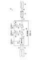
図4は、本開示に従った、例示の電力増幅器14が更に詳細に図示されている図1の例示のトランスミッタ10のブロック図である。電力増幅器14は、選択回路60、増幅器段62、64、調整可能な電源66、68、接続70、72、電力線74、76、及び利得制御リード78、80、82を含む。選択回路60の第1の入力が、接続20を介してオシレータ12の第1の出力に結合される。選択回路60の第2の入力が、接続22を介してオシレータ12の第2の出力に結合される。選択回路60の出力が、接続70を介して増幅器段62の入力に結合される。増幅器段62の出力が、接続72を介して増幅器段64の入力に結合される。増幅器段64の出力が、接続24を介してマッチングネットワーク16の入力に結合される。
FIG. 4 is a block diagram of an
増幅器段64の出力は、電力増幅器14の出力に結合され得、及び/又は電力増幅器14の出力を形成し得る。選択回路60の第1及び第2の入力は、それぞれ、電力増幅器14の第1及び第2の入力に結合され得、及び/又は電力増幅器14の第1及び第2の入力を形成し得る。
The output of the
調整可能な電源66の出力が、電力線74を介して増幅器段62の電力入力に結合される。調整可能な電源68の出力が、電力線76を介して増幅器段64の電力入力に結合される。選択回路60の制御入力が、利得制御Aリード78に結合される。増幅器段62の制御入力が、利得制御Bリード80に結合される。増幅器段64の制御入力が、利得制御Cリード82に結合される。利得制御リード78、80、82は集合的に、図1〜図3に図示される利得制御リード26に対応し得る。
The output of the
接続20、22、24、28、70、72は、シングルエンド接続又は差動接続であり得る。接続20、22がシングルエンド接続であるとき、オシレータ12は、幾つかの例において、図2におけるオシレータ12に対応し得、接続20、22は、図2のリード42、44に対応し得る。オシレータ12の接続20、22が差動接続であるとき、オシレータ12は、幾つかの例において、図3におけるオシレータ12に対応し得、接続20、22は、図3のリード42、44、56、58に対応し得る。
動作の間、選択回路60は、それぞれ、接続20、22を介してオシレータ12から振動信号を受信し、利得制御A信号に基づいて、電力増幅された信号の生成に用いるために振動信号の1つを選択し、選択された信号を接続70上に出力する。増幅器段62は、選択された信号を接続70を介して受信し、選択された信号を利得制御B信号によって決定される利得を用いて増幅し、増幅された信号を接続72上に出力する。増幅器段64は、増幅された信号を接続72を介して増幅器段62から受信し、その信号を、利得制御C信号によって決定される利得を用いて増幅し、増幅された信号を、電力増幅器14に対する電力供給され増幅された信号として、接続24において出力する。
During operation, the selection circuit 60 receives the vibration signal from the
調整可能な電源66は、電力線74を介して増幅器段62に電力供給し得る。同様に、調整可能な電源68は、電力線76を介して増幅器段64に電力供給し得る。調整可能な電源66は、利得制御B信号に基づいて出力電力レベル(例えば、電圧レベル)を生成し得、調整可能な電源68は、利得制御C信号に基づいて出力電力レベル(例えば、電圧レベル)を生成し得る。幾つかの例において、調整可能な電源66、68の一方又は両方が、例えば調整可能なLDO等の調整可能な電圧レギュレータであり得る。増幅器段62は、選択された信号を、調整可能な電源66によって生成された出力電力レベルによって決定される利得に基づいて増幅し得る。増幅器段64は、増幅器段64の入力信号を、調整可能な電源68によって生成された出力電力レベルによって決定される利得に基づいて増幅し得る。
The
図4に示されるように、電力増幅器14は選択回路60を含む。選択回路60は、(1)電力増幅器14の第1の入力に結合される第1の入力、(2)電力増幅器14の第2の入力に結合される第2の入力、及び(3)出力を有する。電力増幅器14は更に増幅器段62を含み、増幅器段62は、(1)選択回路60の出力に結合される入力、及び(2)出力を有する。電力増幅器14は更に増幅器段64を含み、増幅器段64は、(1)増幅器段62の出力に結合される入力、及び(2)出力を有する。選択回路60は、利得制御Aリード78に結合される制御入力を有する。
As shown in FIG. 4, the
増幅器段62、64は、本開示に説明される増幅器段の任意の組み合わせを備えて、又はその他のタイプの増幅器段を備えて実装され得る。幾つかの例において、増幅器段62は、図13に図示される増幅器段を備えて実装され得、増幅器段64は、図14に図示される増幅器段を備えて実装され得る。
The amplifier stages 62, 64 may be implemented with any combination of amplifier stages described herein, or with other types of amplifier stages. In some examples, the
幾つかの例において、電力増幅器14における増幅器段62、64の各々は、シングルエンド又は差動自己バイアス増幅器(例えば、自己バイアスインバータ)を含み得る。増幅器段62、64の各々は更に、それぞれ、調整可能な電源66、68によって提供される、独立して調整可能な電力レール電圧を有し得る。特定の増幅器段に対して電力レール電圧を調整することによって、その段の自己バイアス増幅器が、異なるバイアス電流でバイアスされ得、それによって自己バイアス増幅器の利得が調整され得る。従って、異なる自己バイアス増幅器段に対して、独立して調整可能な電力レール電圧を用いることによって、相対的に少ない数の回路構成要素を用いて、段独立利得調整を備える多段電力増幅器が達成され得る。
In some examples, each of the amplifier stages 62, 64 in the
幾つかの例において、利得制御A信号は、電力増幅された出力信号の生成にどのオシレータ電圧を用いるかの選択を制御する、コース利得制御であり得る。そのような例において、利得制御B信号及び利得制御C信号は集合的に、多段電力増幅器14において増幅器段62、64の利得を制御するファイン利得制御を構成し得る。ファイン利得制御は、幾つかの例において、連続利得制御関数を提供し得るが、利得制御関数が線形である利得値の範囲は相対的に小さくなり得る。一方、コース利得制御関数は、相対的に大きい利得値の範囲にわたって線形であり得るが、離散利得ステップを備える離散関数であり得る。
In some examples, the gain control A signal can be a course gain control that controls the choice of which oscillator voltage to use to generate the power amplified output signal. In such an example, the gain control B signal and the gain control C signal can collectively constitute fine gain control that controls the gains of the amplifier stages 62 and 64 in the
コース及びファイン両方の利得制御を提供することによって、電力増幅器の利得を、幅広い利得値範囲にわたって微細に調整することが可能になり得る。このように、出力電力設定の相対的に大きい範囲にわたって、相対的に高精度の利得制御を持つ電力増幅器が達成され得る。 By providing both course and fine gain control, it may be possible to fine-tune the gain of the power amplifier over a wide gain value range. In this way, a power amplifier with relatively high accuracy gain control can be achieved over a relatively large range of output power settings.
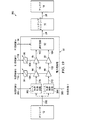
図5は、本開示に従った、別の例示の電力増幅器14が更に詳細に図示されている図1の例示のトランスミッタ10のブロック図である。電力増幅器14は、増幅器段84、86、88、90、選択回路92、調整可能な電源94、96、接続98、100、102、104、電力線106、108、110、112、及び利得制御リード114、116、118を含む。
FIG. 5 is a block diagram of an
増幅器段84の入力が、接続20を介してオシレータ12の第1の出力に結合される。増幅器段84の出力が、接続98を介して増幅器段86の入力に結合される。増幅器段86の出力が、接続100を介して選択回路92の第1の入力に結合される。増幅器段88の入力が、接続22を介してオシレータ12の第2の出力に結合される。増幅器段88の出力が、接続102を介して増幅器段90の入力に結合される。増幅器段90の出力が、接続104を介して選択回路92の第2の入力に結合される。選択回路92の出力が、接続24を介してマッチングネットワーク16の入力に結合される。
The input of the
選択回路92の出力は、電力増幅器14の出力に結合され得、及び/又は電力増幅器14の出力を形成し得る。増幅器段84の入力は、電力増幅器14の第1の入力に結合され得、及び/又は電力増幅器14の第1の入力を構成し得る。同様に、増幅器段88の入力は、電力増幅器14の第2の入力に結合され得、及び/又は電力増幅器14の第2の入力を形成し得る。
The output of the
調整可能な電源94の出力が、電力線106を介して増幅器段84の電力入力に結合される。調整可能な電源94の出力はまた、電力線106、110を介して増幅器段88の電力入力に結合される。調整可能な電源96の出力が、電力線108を介して増幅器段86の電力入力に結合される。調整可能な電源96の出力はまた、電力線108、112を介して増幅器段90の電力入力に結合される。選択回路92の制御入力が利得制御Aリード114に結合される。調整可能な電源94の制御入力が利得制御Bリード116に結合される。調整可能な電源96の制御入力が利得制御Cリード118に結合される。利得制御リード114、116、118は集合的に、図1〜図3に図示される利得制御リード26に対応し得る。
The output of the
接続20、22、24、28、98、100、102、104は、シングルエンド接続又は差動接続であり得る。接続20、22がシングルエンド接続であるとき、オシレータ12は、幾つかの例において、図2におけるオシレータ12に対応し得、接続20、22は、図2のリード42、44に対応し得る。オシレータ12の接続20、22が差動接続であるとき、オシレータ12は、幾つかの例において、図3におけるオシレータ12に対応し得、接続20、22は、図3のリード42、44、56、58に対応し得る。
動作の間、増幅器段84は、第1の入力を介して第1の振動信号を受信し、第1の増幅された信号を生成するために第1の振動信号を増幅し、第1の増幅された信号を接続98を介して出力する。増幅器段86は、第1の増幅された信号を接続98を介して受信し、第2の増幅された信号を生成するために第1の増幅された信号を増幅し、第2の増幅された信号を接続100を介して出力する。増幅器段86は、第2の入力を介して第2の振動信号を受信し、第3の増幅された信号を生成するために第2の振動信号を増幅し、第3の増幅された信号を接続102を介して出力する。増幅器段86は、第1の増幅された信号を接続102を介して受信し、第4の増幅された信号を生成するために第3の増幅された信号を増幅し、第4の増幅された信号を接続104を介して出力する。選択回路92は、それぞれ、接続100及び接続104を介して第3及び第4の増幅された信号を受信し、電力増幅された信号を利得制御A信号に基づいて生成するために用いるために第3及び第4の増幅された信号の一方を選択し、選択された信号を接続24を介して出力する。
During operation, the
増幅器段84、86は第1の増幅器信号チェーンを形成し得、増幅器段88、90は第2の増幅器信号チェーンを形成し得る。第1の増幅器信号チェーンは、接続20において受信した振動信号を増幅し得、第2の増幅器信号チェーンは、接続22において受信した振動信号を増幅し得、選択回路92は増幅された信号のいずれを電力増幅された信号として出力するかを選択し得る。
The amplifier stages 84, 86 may form a first amplifier signal chain, and the amplifier stages 88, 90 may form a second amplifier signal chain. The first amplifier signal chain may amplify the vibration signal received at
調整可能な電源94は、電力線106、110を介して増幅器段84、88に電力供給し得る。同様に、調整可能な電源96は、電力線108、112を介して増幅器段86、90に電力供給し得る。調整可能な電源94は利得制御B信号に基づいて出力電力レベル(例えば、電圧レベル)を生成し得、調整可能な電源96は利得制御C信号に基づいて出力電力レベル(例えば、電圧レベル)を生成し得る。幾つかの例において、調整可能な電源94、96の1つ又は複数が、例えば、調整可能な及び/又はプログラム可能なLDO等、調整可能な及び/又はプログム可能な電力増幅された信号を電圧レギュレータであり得る。増幅器段84、88は、調整可能な電源94によって生成された出力電力レベルによって決定される利得に基づいて、それらのそれぞれの入力信号を増幅し得る。同様に、増幅器段86、90は、調整可能な電源96によって生成された出力電力レベルによって決定される利得に基づいて、それらのそれぞれの入力信号を増幅し得る。
The
図5に示されるように、電力増幅器14は、増幅器段84、86を有する第1の信号チェーンを含む。増幅器段84は、(1)電力増幅器14の第1の入力に結合される入力、及び(2)出力を有する。増幅器段86は、(1)第1の信号チェーンの増幅器段84の出力に結合される入力、及び(2)出力を有する。電力増幅器14は更に、増幅器段88、90を有する第2の信号チェーンを含む。増幅器段88は、(1)電力増幅器の第2の入力に結合される入力、及び(2)出力を有する。増幅器段90は、(1)第2の信号チェーンの第1の増幅器段88の出力に結合される入力、及び(2)出力を有する。
As shown in FIG. 5, the
電力増幅器14は更に選択回路92を含み、選択回路92は、(1)第1の信号チェーンの増幅器段86の出力に結合される第1の入力、(2)第2の信号チェーンの増幅器段90の出力に結合される第2の入力、及び(3)電力増幅器14の出力を形成する出力を有する。選択回路92は、利得制御Aリード114に結合される制御入力を有する。
The
増幅器段84、86、88、90は、本開示に説明される増幅器段の任意の組み合わせを備えて又はその他のタイプ増幅器段を備えて実装され得る。幾つかの例において、増幅器段84、88は、図13に図示される増幅器段を備えて実装され得、増幅器段86、90は、図14に図示される増幅器段を備えて実装され得る。 Amplifier stages 84, 86, 88, 90 may be implemented with any combination of amplifier stages described herein or with other types of amplifier stages. In some examples, amplifier stages 84, 88 may be implemented with the amplifier stages shown in FIG. 13, and amplifier stages 86, 90 may be implemented with the amplifier stages shown in FIG.
幾つかの例において、電力増幅器14の増幅器段84、86、88、90の各々は、シングルエンド又は差動自己バイアス増幅器(例えば、自己バイアスインバータ)を含み得る。増幅器段84、86、88、90の各々は更に、調整可能な電源94、96によって提供される独立して調整可能な電力レール電圧を有し得る。特定の増幅器段に対して電力レール電圧を調整することによって、その段の自己バイアス増幅器が、異なるバイアス電流でバイアスされ得、それによって自己バイアス増幅器の利得が調整され得る。従って、異なる自己バイアス増幅器段に対して、独立して調整可能な電力レール電圧を用いることによって、相対的に少ない数の回路構成要素を用いて、段独立利得調整を備える多段電力増幅器が達成され得る。
In some examples, each of the amplifier stages 84, 86, 88, 90 of the
幾つかの例において、利得制御A信号は、電力増幅された出力信号の生成に、どのオシレータ電圧を用いるかの選択を制御する、コース利得制御であり得る。そのような例において、利得制御B信号及び利得制御C信号は集合的に、多段電力増幅器14において増幅器段84、86、88、90の利得を制御するファイン利得制御を構成し得る。ファイン利得制御は、幾つかの例において、連続利得制御関数を提供し得るが、利得制御関数が線形である利得値の範囲は相対的に小さくなり得る。一方、コース利得制御関数は、相対的に大きい利得値の範囲にわたって線形であり得るが、離散利得ステップを備える離散関数であり得る。
In some examples, the gain control A signal can be a course gain control that controls the choice of which oscillator voltage to use to generate the power amplified output signal. In such an example, the gain control B signal and the gain control C signal can collectively constitute fine gain control that controls the gains of the amplifier stages 84, 86, 88, 90 in the
コース及びファイン両方の利得制御を提供することによって、電力増幅器の利得を幅広い範囲にわたって微細に調整することが可能になり得る。このように、出力電力設定の相対的に大きい範囲にわたって、相対的に高精度の利得制御を持つ電力増幅器が達成され得る。 By providing both course and fine gain control, it may be possible to fine-tune the gain of the power amplifier over a wide range. In this way, a power amplifier with relatively high accuracy gain control can be achieved over a relatively large range of output power settings.
図6は、本開示の例示のオシレータにおいて用いられ得る例示のリアクティブ構成要素ネットワーク34を図示する概略図である。幾つかの例において、リアクティブ構成要素ネットワーク34は、図3において図示されるリアクティブ構成要素ネットワーク34を実装するために用いられ得る。リアクティブ構成要素ネットワーク34はインダクタL1、L2、L3、L4、及びノード36、38、120、122、124を含む。インダクタL1はノード36とノード120との間に結合される。インダクタL2は、ノード120とノード122との間に結合される。インダクタL3は、ノード122とノード124との間に結合される。インダクタL4は、ノード124とノード38との間に結合される。
FIG. 6 is a schematic diagram illustrating an exemplary
タップ54がノード120に結合され、タップ40がノード124に結合される。ノード36、38は第1の差動出力を形成し得、タップ54、40は第2の差動出力を形成し得る。
The
図6に示されるように、タップ54、40は、ノード36とノード38との間のノード120、124に結合される。そのため、ノード36とノード38との間のインダクタンスは、リアクティブ構成要素ネットワーク34のタップ54とタップ40との間のインダクタンスより大きく、それにより、タップ54とタップ40との間の電圧を、ノード36とノード38と間の電圧に比例させるが、ノード36とノード38と間の電圧より小さくする。
As shown in FIG. 6, taps 54, 40 are coupled to
図7は、本開示に従った、図6の例示のリアクティブ構成要素ネットワーク34を組み込む例示のオシレータ12を図示する概略図である。オシレータ12は、トランジスタ126、128、接地レール130、高電圧レール132、及び図6に示されるリアクティブ構成要素ネットワーク34を含む。トランジスタ126のソースが接地レール130に結合される。トランジスタ126のドレインが、ノード36に及びトランジスタ128のゲートに結合される。トランジスタ126のゲートが、ノード38に及びトランジスタ128のドレインに結合される。トランジスタ128のソースが接地レール130に結合される。トランジスタ128のドレインが、ノード38に及びトランジスタ126のゲートに結合される。トランジスタ128のゲートが、ノード36に及びトランジスタ126のドレインに結合される。リアクティブ構成要素ネットワーク34のノード122は高電圧レール132に結合される。
FIG. 7 is a schematic diagram illustrating an
トランジスタ126、128はクロス結合トランジスタの例であり得、クロス結合トランジスタの出力がノード36、38に結合される。ノード36、38はオシレータ12に対する第1の差動出力を形成し、タップ40、54はオシレータ12に対する第2の差動出力を形成する。図7において、インダクタL 1、L2、L3、L4は、オシレータ12のノード36とノード38との間で直列に結合される1つ又は複数のインダクタの構成の例である。
動作の間、トランジスタ126、128は各々、リアクティブ負荷を備える共通ソース増幅器として動作し得る。インダクタL 1、L2、L3、L4は、トランジスタ126、128に対するリアクティブ負荷の全部又は一部を形成し得る。具体的には、トランジスタ126は、トランジスタ128のドレインにおける信号を増幅し得、信号に180度位相シフトを適用し得る。トランジスタ128は、トランジスタ126のドレインにおける信号を増幅し得、信号に180度位相シフトを適用し得る。クロス結合オシレータによって形成されるフィードバックループは集合的に、ノード36、38における2つの差動出力における信号を振動させ得る。インダクタL 1、L2、L3、L4のインダクタンスは、トランジスタ126、128における1つ又は複数の寄生キャパシタンスと共に、オシレータ12に対する振動の周波数を制御し得る。
During operation,
タップ40、54によって形成されるオシレータ12の第2の差動出力は、ノード36、38によって形成されるオシレータ12の第1の差動出力によって提供される出力信号に比例するが、それより小さい振動出力信号を提供し得る。これらの電圧のどれを増幅するかを選択することによって、電力増幅器の利得を変化させることが可能であり得る。異なる電圧の電圧レベルを出力するために、オシレータ12に含まれるリアクティブ構成要素のネットワーク(例えば、インダクタL 1、L2、L3、L4)の1つ又は複数のタップを用いることによって、電力増幅器において又は集積回路の外部に、付加的なリアクティブ構成要素を必要とすることなく、電力増幅器の利得を変化させることが可能になり得る。このように、相対的に少ない数の構成要素を用いて、可変利得の、相対的に低電力の増幅器が得られ得る。
The second differential output of
図8は、本開示の例示のオシレータに用いられ得る別の例示のリアクティブ構成要素ネットワーク34を図示する概略図である。リアクティブ構成要素ネットワーク34は、インダクタL5、L6、L7、L8、L9、L10、ノード134、136、138、140、142、144、146、及びタップ148、150、152、154を含む。インダクタL5は、ノード134とノード136との間に結合される。インダクタL6は、ノード136とノード138との間に結合される。インダクタL7は、ノード138とノード140との間に結合される。インダクタL8は、ノード140とノード142との間に結合される。インダクタL9は、ノード142とノード144との間に結合される。インダクタL10は、ノード144とノード146との間に結合される。図8において、インダクタL5、L6、L7、L8、L9、L10は、オシレータ12のノード134とノード146との間に直列に結合される1つ又は複数のインダクタの構成の例である。
FIG. 8 is a schematic diagram illustrating another exemplary
タップ148はノード136に結合される。タップ150はノード138に結合される。タップ152はノード142に結合される。タップ154はノード144に結合される。
ノード134、146は第1の差動出力を形成し得、タップ136、144は第2の差動出力を形成し得、タップ138、142は第3の差動出力を形成し得る。第2の差動出力は、第1の差動出力によって出力される信号に比例するが、それより小さい、振動信号を出力し得る。第3の差動出力は、第1及び第2の差動出力によって出力される信号に比例するが、それより小さい、振動信号を出力し得る。概して、任意の数の差動出力を形成するため、またそれによって、本開示に従って電力増幅器に対して任意の数の利得ステップを提供するために、直列に接続された一連のインダクタにおいて、任意の数のタップが配置され得る。
図9は、本開示の例示のトランスミッタに用いられ得る例示のリアクティブ構成要素及びスイッチング回路156の概略図である。幾つかの例において、リアクティブ構成要素ネットワーク34は、図3に示されるリアクティブ構成要素ネットワーク34及び/又は図4に示される選択回路60を実装するために用いられ得る。リアクティブ構成要素及びスイッチング回路156は、インダクタL11、L12、L13、スイッチS1、S2、S3、S4、及びノード158、160、162、164、166、168を含む。
FIG. 9 is a schematic representation of an exemplary reactive component and switching
インダクタL11は、ノード158とノード160との間に結合される。インダクタL12は、ノード160とノード162との間に結合される。インダクタL13は、ノード162とノード164との間に結合される。スイッチS1は、ノード158とノード166との間に結合される。スイッチS2は、ノード160とノード166との間に結合される。スイッチS3は、ノード162とノード168との間に結合される。スイッチS4は、ノード164とノード168との間に結合される。
The inductor L11 is coupled between the
ノード158、164は差動入力を形成し得る。ノード166、168は差動出力を形成し得る。
幾つかの例において、インダクタLll、L12、L13及びノード158、160、162、164は、オシレータ12(例えば、図3)のリアクティブ構成要素ネットワーク34に含まれ得、スイッチS1、S2、S3、S4は、電力増幅器14(例えば、図4)の選択回路60に含まれ得る。そのような例において、ノード158、164は、それぞれ、ノード36、38に対応し得、ノード166、168は選択回路60の出力に対応し得る。そのような例において、スイッチS1、S2、S3、S4の制御入力は、利得制御Aリード78に結合され得る。
In some examples, the inductors Lll, L12, L13 and the
動作の間、制御回路が、利得制御信号に基づいてスイッチS1、S2、S3、S4を選択的に開閉し得る。第1の動作状態の間、スイッチS1、S4は閉にされ得、スイッチS2、S3は開にされ得、それによって、ノード158とノード164との間の電圧がノード166、168において出力される。第2の動作状態の間、スイッチS2、S3は閉にされ得、スイッチS1、S4は開にされ得、それによって、ノード160とノード162との間の電圧がノード166、168において出力される。
During operation, the control circuit may selectively open and close switches S1, S2, S3, S4 based on the gain control signal. During the first operating state, switches S1 and S4 may be closed and switches S2 and S3 may be open so that the voltage between
幾つかの例において、インダクタL11、L12、L13はタップ付きインダクタを形成し得る。タップ付きインダクタは、スイッチS1、S2、S3、S4と共に、VCOとPAとの間に利得ステップを提供し得る。幾つかの例において、インダクタL11、L12、L13は、VCOコアの内部にインダクタを備えて実装され得、スイッチS1、S2、S3、S4は減衰器ステップを提供し得る。 In some examples, the inductors L11, L12, L13 may form a tapped inductor. The tapped inductor, along with the switches S1, S2, S3, S4, may provide a gain step between the VCO and PA. In some examples, inductors L11, L12, L13 may be mounted with inductors inside the VCO core, and switches S1, S2, S3, S4 may provide an attenuator step.
図10は、本開示の例示のオシレータに用いられ得る、別の例示のリアクティブ構成要素ネットワーク34を図示する概略図である。リアクティブ構成要素ネットワーク34は、キャパシタC1、C2、C3、C4、C5、C6、C7、C8、スイッチS5、S6、ノード170、172、174、176、178、180、182、184、186、188、及びタップ190、192、194、196を含む。キャパシタC1は、ノード170とノード172との間に結合される。キャパシタC2は、ノード172とノード174との間に結合される。キャパシタC3は、ノード178とノード180との間に結合される。キャパシタC4は、ノード176とノード178との間に結合される。キャパシタC5は、ノード172とノード182との間に結合される。キャパシタC6は、ノード178とノード186との間に結合される。キャパシタC7は、ノード174とノード184との間に結合される。キャパシタC8は、ノード176とノード188との間に結合される。スイッチS5は、ノード182とノード186との間に結合される。スイッチS6は、ノード184とノード188との間に結合される。タップ190はノード172に結合され、タップ192はノード174に結合され、タップ194はノード176に結合され、タップ196はノード178に結合される。
FIG. 10 is a schematic diagram illustrating another exemplary
ノード170及びノード180は、リアクティブ構成要素ネットワーク34の端部を形成し得、リアクティブ構成要素ネットワーク34の第1の差動出力に対応し得る。タップ190、196はリアクティブ構成要素ネットワーク34の第2の差動出力を形成し得、タップ192、194はリアクティブ構成要素ネットワーク34の第3の差動出力を形成し得る。
図10に示されるように、タップ192、194は、タップ190とタップ196との間で、及びノード170とノード180との間で、リアクティブ構成要素ネットワーク34に結合される。同様に、タップ190、196は、ノード170とノード180との間で、リアクティブ構成要素ネットワーク34に結合される。そのため、ノード170とノード180との間のキャパシタンスは、(スイッチS5、S6の一方が閉にされるとき)タップ190とタップ196との間のキャパシタンスより大きく、それによって、タップ190とタップ196との間の電圧が、ノード170とノード180との間の電圧に比例するが、それより小さくなる。同様に、ノード170とノード180との間のキャパシタンスは、(スイッチS6が閉にされるとき)タップ190とタップ196との間のキャパシタンスより大きく、タップ190とタップ196との間のキャパシタンスは、(スイッチS6が閉にされるとき)タップ192とタップ194との間のキャパシタンスより大きく、それによって、タップ192とタップ194との間の電圧が、タップ190とタップ196との間の電圧及びノード170とノード180との間の電圧に比例するが、それらより小さくなる。
As shown in FIG. 10, taps 192 and 194 are coupled to the
図11は、本開示に従った、図10の例示のリアクティブ構成要素ネットワーク34を組み込む例示のオシレータ12を図示する概略図である。オシレータ12は、トランジスタ198、200、インダクタL14、L15、接地レール202、高電圧レール204、ノード206、及び図10に示されるリアクティブ構成要素ネットワーク34を含む。トランジスタ198のソースが接地レール202に結合される。トランジスタ198のドレインが、ノード170に及びトランジスタ200のゲートに結合される。トランジスタ198のゲートが、ノード180に及びトランジスタ200のドレインに結合される。トランジスタ200のソースが接地レール202に結合される。トランジスタ200のドレインが、ノード180に及びトランジスタ198のゲートに結合される。トランジスタ200のゲートが、ノード170に及びトランジスタ198のドレインに結合される。インダクタL14は、ノード170とノード206との間に結合される。インダクタL15は、ノード206とノード180との間に結合される。ノード206は高電圧レール204に結合される。
FIG. 11 is a schematic diagram illustrating an
トランジスタ198、200はクロス結合トランジスタの例であり得、クロス結合トランジスタの出力がノード36、38に結合される。スイッチS5、S6は、制御回路に結合される制御入力を含む。図11において、スイッチS5、S6の一方が閉にされるとき、ノード170とノード180との間のキャパシタンスは、オシレータ12のノード170とノード180との間に直列に結合される1つ又は複数のキャパシタの構成の例であり得る。
動作の間、トランジスタ198、200は各々、リアクティブ負荷を備える共通ソース増幅器として動作し得る。キャパシタC1、C2、C3、C4、C5、C6、C7、C8、及びインダクタL14、L15は、トランジスタ198、200に対するリアクティブ負荷の全部又は一部を形成し得る。具体的には、トランジスタ198は、トランジスタ200のドレインにおける信号を増幅し得、この信号に180度位相シフトを適用し得る。トランジスタ200は、トランジスタ198のドレインにおける信号を増幅し得、この信号に180度位相シフトを適用し得る。クロス結合オシレータによって形成されるフィードバックループは、集合的に、ノード170、180における2つの差動出力における信号を振動させ得る。インダクタL14、L15のインダクタンスは、キャパシタC1、C2、C3、C4、C5、C6、C7、C8の1つ又は複数のキャパシタンス(及び、幾つかの例において、トランジスタ198、200における1つ又は複数の寄生キャパシタンス)と共に、オシレータ12に対する振動の周波数を制御し得る。
During operation,
スイッチS5、S6は、オシレータ12の振動周波数をプログラムするように、選択的に開閉され得る。スイッチS5、S6に対する開閉状態の任意の組み合わせは、異なる振動周波数に対応し得る。
The switches S5, S6 can be selectively opened and closed to program the vibration frequency of the
タップ192、194によって形成されるオシレータ12の第3の差動出力は、振動出力信号を提供し得、その振動出力信号は、タップ190、196によって形成されるオシレータ12の第2の差動出力によって提供される出力信号に比例するが、それより小さく、タップ190、196によって形成されるオシレータ12の第2の差動出力によって提供される出力信号は、ノード170、180によって形成されるオシレータ12の第1の差動出力によって提供される出力信号に比例するが、それより小さい。増幅するためにどの電圧を選択するかによって、電力増幅器の利得を変化させることが可能であり得る。異なる電圧の電圧レベルを出力するために、オシレータ12に含まれるリアクティブ構成要素のネットワークの1つ又は複数のタップ(例えば、キャパシタC1、C2、C3、C4、C5、C6、C7、C8)を用いることにより、電力増幅器において又は集積回路の外部に、付加的なリアクティブ構成要素を必要とすることなく、電力増幅器の利得を変化させることができる。このようにして、相対的に少ない数の構成要素を用いて、可変利得の、相対的に低電力増幅器が得られ得る。
The third differential output of the
図12は、本開示の例示のオシレータにおいて用いられ得る、別の例示のリアクティブ構成要素ネットワーク208を図示する概略図である。リアクティブ構成要素ネットワーク208は、キャパシタC9、C10、C11、C12、C13、C14、スイッチS7、S8、S9、S10、及びノード210、212、214、216、218、220を含む。キャパシタC9は、ノード210とノード212との間に結合される。キャパシタC10は、ノード212とノード214との間に結合される。キャパシタC11は、ノード216とノード218との間に結合される。キャパシタC12は、ノード218とノード220との間に結合される。キャパシタC13は、スイッチS7とスイッチS8との間に結合される。キャパシタC14は、スイッチS9とスイッチS10との間に結合される。スイッチS7は、キャパシタC13とノード212との間に結合される。スイッチS8は、キャパシタC13とノード218との間に結合される。スイッチS9は、キャパシタC14とノード212との間に結合される。スイッチS10は、キャパシタC14とノード218との間に結合される。
FIG. 12 is a schematic diagram illustrating another exemplary
幾つかの例において、図12におけるリアクティブ構成要素ネットワーク208は、本開示のコース利得制御回路において用いられ得る容量減衰回路を実装し得る。容量減衰回路は、トランスミッタにおいて、VCOと電力増幅器との間に利得を提供し得る。幾つかの例において、リアクティブ構成要素ネットワーク208は、VCOコアの内部のキャパシタと組み合わせられ得、スイッチS7、S8、S9、S10は、減衰器ステップを提供し得る。
In some examples, the
図13は、本開示の電力増幅器において用いられ得る例示の増幅器段230を図示する概略図である。増幅器段230は、トランジスタ232、234、236、238、調整可能なLDO240、抵抗器242、244、246、248、バイアス抵抗器250、252、調整可能な抵抗254、256、キャパシタ258、260、接地レール262、及びノード264、266、268、270、272、274、276、278を含む。
FIG. 13 is a schematic diagram illustrating an
トランジスタ232は、抵抗器242とノード268との間に結合される。具体的には、トランジスタ232のソースが抵抗器242に結合され、トランジスタ232のドレインがノード268に結合される。トランジスタ232のゲートがノード276に結合される。トランジスタ234は、抵抗器246とノード268との間に結合される。具体的には、トランジスタ234のソースが抵抗器246に結合され、トランジスタ234のドレインがノード268に結合される。トランジスタ234のゲートがノード276に結合される。
The
トランジスタ236は、抵抗器244とノード270との間に結合される。具体的には、トランジスタ236のソースが抵抗器244に結合され、トランジスタ236のドレインがノード270に結合される。トランジスタ236のゲートがノード278に結合される。トランジスタ238は、抵抗器248とノード270との間に結合される。具体的には、トランジスタ238のソースが抵抗器248に結合され、トランジスタ238のドレインがノード270に結合される。トランジスタ238のゲートがノード278に結合される。
The
抵抗器242は、トランジスタ232とノード272との間に結合される。抵抗器244は、トランジスタ236とノード272との間に結合される。抵抗器246は、トランジスタ234とノード274との間に結合される。抵抗器248は、トランジスタ238とノード274との間に結合される。バイアス抵抗器250は、ノード268とノード276との間に結合される。バイアス抵抗器252は、ノード270とノード278との間に結合される。
The
調整可能な抵抗254は、調整可能なLDO240の出力とノード272との間に結合される。調整可能な抵抗256は、ノード274と接地レール262との間に結合される。キャパシタ258は、ノード264とノード276との間に結合される。キャパシタ260は、ノード266とノード278との間に結合される。
The
トランジスタ232、234及びバイアス抵抗器250は、第1の自己バイアス増幅器(例えば、自己バイアスインバータ)を形成する。トランジスタ236、238及びバイアス抵抗器252は、第2の自己バイアス増幅器(例えば、自己バイアスインバータ)を形成する。トランジスタ232、234、236、238及びバイアス抵抗器250、252は共に、差動自己バイアス増幅器(例えば、差動自己バイアスインバータ)を形成する。
The
ノード264、266は増幅器段230に対する差動入力を形成し得、ノード268、270は、増幅器段230に対する差動出力を形成し得る。具体的には、ノード264は非反転入力を形成し得、ノード266は反転入力を形成し得る。同様に、ノード268は非反転出力を形成し得、ノード270は反転出力を形成し得る。
図13に示されるように、増幅器段230は、(1)電力レール(例えば、調整可能なLDO240の出力に結合されるリード)、調整可能な抵抗254、(2)調整可能な抵抗254を介して電力レールに結合される第1の自己バイアスインバータ(例えば、トランジスタ232、234、及び抵抗器250)、及び(3)調整可能な抵抗254を介して電力レール(例えば、調整可能なLDO240の出力)に結合される第2の自己バイアスインバータ(例えば、トランジスタ236、238、及び抵抗器252)を含む。電力レールは、例えば、調整可能なLDO240等の調整可能な電源に結合される。増幅器段230は更に、調整可能な抵抗256を含む。第1の自己バイアスインバータ(例えば、トランジスタ232、234、及び抵抗器250)は、調整可能な抵抗256を介して接地レール262に結合され、第2の自己バイアスインバータ(例えば、トランジスタ236、238、及び抵抗器252)は、調整可能な抵抗256を介して接地レール262に結合される。
As shown in FIG. 13, the
第1の自己バイアスインバータは、入力(例えば、ノード276)、出力(例えば、ノード268)、及び第1の自己バイアスインバータの入力と出力との間に結合されるバイアス抵抗器250を含む。第2の自己バイアスインバータは、入力(例えば、ノード278)、出力(例えば、ノード270)、及び第2の自己バイアスインバータの入力と出力との間に結合されるバイアス抵抗器252を含む。
The first self-bias inverter includes an input (eg, node 276), an output (eg, node 268), and a
動作の間、バイアス抵抗器250、252は、自己バイアスインバータを、調整可能なLDO240によって出力される電圧と接地との間のおよそ中間である電圧でバイアスする。キャパシタ258、260は、ノード264、266において受け取られる直流(DC)及びその他の低周波数信号成分をフィルタリング除去する。トランジスタ232、234、236、238によって形成される増幅器は、キャパシタ258、260から受信されたフィルタリングされた入力信号を増幅し、増幅された信号をノード268、270において出力する。
During operation, the
幾つかの例において、増幅器段230は、自己バイアスAB級PA段を実装し得る。調整可能な抵抗254、256はPA段の電流消費を制御し得、及びVCOからの第2の高調波音の拒絶を提供し得、一方、抵抗器242、244、246、248は、付加的な高調波が実質的に生成されないように、段に対して線形性を提供し得る。
In some examples, the
幾つかの例において、調整可能な抵抗254、256にコース利得制御が結合され得、調整可能なLDO240にファイン利得制御が結合され得る。付加的な例において、調整可能なLDO240は、可変ではない固定電力供給とし得る。
In some examples, the
調整可能な抵抗254、256の抵抗を増加させることは、増幅器段230の偶数次高調波抑圧を増加させ得るが、増幅器段230の利得を低減させ得る。調整可能な抵抗254、256の抵抗を低減させることは、反対の効果を有し得る。そのため、調整可能な抵抗254、256を図13において図示される箇所に置くことによって、偶数次高調波抑圧と増幅器利得との間のトレードオフが、増幅器段230において動的に調整及び均衡され得る。
Increasing the resistance of the
図14は、本開示の電力増幅器において用いられ得る、別の例示の増幅器段280を図示する概略図である。増幅器段280は、トランジスタ282、284、調整可能なLDO286、スイッチ288、290、292、294、296、バイアス抵抗器298、300、302、キャパシタ304、306、接地レール308、及びノード310、312、314、316、318、320、322、324、326、328を含む。
FIG. 14 is a schematic diagram illustrating another
トランジスタ282は、調整可能なLDO286とノード320との間に結合される。具体的には、トランジスタ282のソースが、調整可能なLDO286の出力に結合され、トランジスタ282のドレインがノード320に結合される。トランジスタ282のゲートがノード312に結合される。トランジスタ284は、ノード320と接地レール308との間に結合される。具体的には、トランジスタ284のソースが接地レール308に結合され、トランジスタ284のドレインがノード320に結合される。トランジスタ284のゲートがノード314に結合される。
スイッチ288は、ノード312とノード324との間に結合される。スイッチ290は、ノード312とノード316との間に結合される。スイッチ292は、ノード316とノード318との間に結合される。スイッチ294は、ノード316とノード314との間に結合される。スイッチ296は、ノード314とノード326との間に結合される。バイアス抵抗器298は、ノード318とノード320との間に結合される。バイアス抵抗器300は、ノード322とノード324との間に結合される。バイアス抵抗器302は、ノード326とノード328との間に結合される。キャパシタ304は、ノード310とノード312との間に結合される。キャパシタ306は、ノード310とノード314との間に結合される。ノード322は、第1のバイアス電圧源(V_BIAS_P)に結合され、ノード328は第2のバイアス電圧源(V_BIAS_N)に結合される。
スイッチ290、292、294が閉にされるとき、トランジスタ282、284、及びバイアス抵抗器298は、自己バイアス増幅器(例えば、自己バイアスインバータ)を形成する。ノード310は増幅器段280に対する入力を形成し得、ノード320は増幅器段280に対する出力を形成し得る。
When the
図14に示されるように、増幅器段280は、(1)トランジスタ282及びトランジスタ284を有するインバータ、(2)インバータの出力(例えば、ノード320)に結合されるバイアス抵抗器298、(3)第1のバイアス電圧源(V_BIAS_P)、(4)第2のバイアス電圧源(V_BIAS_N)、(5)バイアス抵抗器298とトランジスタ282のゲートとの間に結合されるスイッチ290、(6)第1のバイアス電圧源(V_BIAS_P)とトランジスタ282のゲートとの間に結合されるスイッチ288、(7)バイアス抵抗器298とトランジスタ284のゲートとの間に結合されるスイッチ294、及び(8)第2のバイアス電圧源(V_BIAS_N)とトランジスタ284のゲートとの間に結合されるスイッチ296を含む。増幅器段280は制御ユニット(図示されない)を含み得、制御ユニットは、スイッチ288、290、292、294、296に結合され、増幅器段280を自己バイアス動作モードと非線形動作モードとの間で切り替えるように構成される。
As shown in FIG. 14, the
自己バイアス動作モードの間、スイッチ290、292、294は閉であり、スイッチ288、296は開である。バイアス抵抗器298は、トランジスタ282、284によって形成されるインバータを、調整可能なLDO286によって出力される電圧と接地との間のおよそ中間の電圧でバイアスする。キャパシタ304、306は、ノード310において受け取った直流(DC)及びその他の周波数信号成分をフィルタリング除去する。トランジスタ282、284によって形成される増幅器は、ノード312、314において受信されたフィルタリングされた入力信号を増幅し、増幅された信号をノード320において出力する。
During the self-bias operation mode, switches 290, 292, 294 are closed and switches 288, 296 are open. The
非線形動作モードの間、スイッチ290、292、294は開であり、スイッチ288、296は閉である。第1のバイアス電圧源(V_BIAS_P)が、バイアス抵抗器300を介してトランジスタ282をバイアスする。第2のバイアス電圧源(V_BIAS_N)が、バイアス抵抗器302を介してトランジスタ284をバイアスする。キャパシタ304、306は、ノード310において受け取った直流(DC)及びその他の周波数信号成分をフィルタリング除去する。トランジスタ282、284によって形成される増幅器は、ノード312、314において受信されたフィルタリングされた入力信号を増幅し、増幅された信号をノード320において出力する。
During the non-linear operating mode, switches 290, 292, 294 are open and switches 288, 296 are closed. The first bias voltage source (V_BIAS_P) biases the
上述したように、増幅器段280は、スイッチ288、290、292、294、296の構成に応じて自己バイアスモード又は非線形モードで動作し得る。自己バイアスモードは、非線形モードに比べ、一層大きい度合の線形性を提供し得るが、電力効率が一層低くなり得る。一方、非線形モードは、電力効率が一層高くなり得るが、一層小さい線形性を提供し得る。自己バイアスモード及び非線形モードで動作するように構成可能であり得る増幅器段を提供することによって、線形性と電力効率との間のトレードオフが、増幅器において動的に調整及び均衡され得る。
As mentioned above, the
図15は、本開示の電力増幅器において用いられ得る、別の例示の増幅器段330を図示する概略図である。増幅器段330は、(1)抵抗器242、244、246、248、及び調整可能な抵抗254、256が省かれていること、及び(2)トランジスタ232、234及びトランジスタ236、238が、別々に調整可能なLDO240に結合されていることを除くと、図13に図示される増幅器段230に類似している。図13と図15との間で同一又は類似の構成要素には、同じ参照番号が付されている。図15に示されるように、トランジスタ232のソースが、介在する抵抗無しで、調整可能なLDO240の第1の出力に直接結合され、トランジスタ236のソースが、介在する抵抗無しで、調整可能なLDO240の第2の出力に直接結合される。
FIG. 15 is a schematic diagram illustrating another
図16は、本開示に従った別の例示のトランスミッタ340を図示するブロック図である。トランスミッタ340は、図16におけるトランスミッタ340が、選択回路60の代わりにコース利得制御回路342を含むことを除くと、図4に示されるトランスミッタ10に類似している。図4と図16との間で同一又は類似の構成要素には、同じ参照番号が付されている。
FIG. 16 is a block diagram illustrating another
コース利得制御回路342の第1の入力が、接続20を介してオシレータ12の第1の出力に結合される。コース利得制御回路342の第2の入力が、接続22を介してオシレータ12の第2の出力に結合される。コース利得制御回路342の出力が、接続70を介して増幅器段62の入力に結合される。コース利得制御回路342の制御入力が、利得制御Aリード78に結合される。
The first input of the course
コース利得制御回路342は、接続20、22を介して受信される信号を減衰するように構成される1つ又は複数の受動減衰回路(例えば、リアクティブ構成要素)を含み得る。受動減衰回路は、容量減衰回路及び/又は誘導減衰回路を含み得る。受動減衰回路は、回路の利得又は減衰のレベルが変化され得る(例えば、出力信号を生成するためにタップの異なる組み合わせを選択する)可変利得受動減衰回路(例えば、複数のタップを備えるリアクティブ構成要素のネットワーク)であり得る。例示の容量減衰回路が、図10及び図12に図示されている。例示の誘導減衰回路が、図6、図8、及び図9に図示されている。
The course
コース利得制御回路342は、接続20、22を介して受信された信号の1つを選択し得、減衰された信号を接続70において生成するように、1つ又は複数の受動減衰回路を用いて信号を減衰させ得る。コース利得制御回路342は、利得制御A信号に基づいて、信号のどれを選択するかを決定し得る。受動減衰回路が可変利得受動減衰回路である場合、コース利得制御回路342は、利得制御A信号に基づいて、受動減衰回路が信号をどの程度減衰するべきかを決定し得る。幾つかの例において、利得制御A信号は、選択する信号を決定する第1の構成要素、及び受動減衰器が信号を減衰する量を決定する第2の構成要素を含み得る。
The course
図17は、本開示に従った別の例示のトランスミッタ350を図示するブロック図である。トランスミッタ350は、(1)図17におけるトランスミッタ350が、図16に示されるようなデュアル入力コース利得制御回路342の代わりにシングル入力コース利得制御回路352を含むこと、及び(2)オシレータ12がシングル出力オシレータ12であることを除くと、図16に示されるトランスミッタ340に類似し得る。図16と図17との間で同一又は類似の構成要素には同じ参照番号が付されている。
FIG. 17 is a block diagram illustrating another
コース利得制御回路352の入力が、接続354を介してオシレータ12の出力に結合される。コース利得制御回路352の出力が、接続70を介して増幅器段62の入力に結合される。コース利得制御回路352の制御入力が利得制御Aリード78に結合される。
The input of the course
コース利得制御回路352は、接続354を介して受信された信号を減衰するように構成される1つ又は複数の受動減衰回路(例えば、リアクティブ構成要素)を含み得る。受動減衰回路は、図16におけるコース利得制御回路342に関連して上述した受動減衰回路のうちの任意のものを含み得る。
The course
コース利得制御回路352は、接続70において減衰された信号を生成するため、接続354を介して受信された信号を1つ又は複数の受動減衰回路を用いて減衰し得る。受動減衰回路が可変利得受動減衰回路である場合、コース利得制御回路352は、受動減衰回路が、利得制御A信号に基づいて、信号をどの程度減衰するべきかを決定し得る。
Since the course
図17は、全体的なトランスミッタアーキテクチャを図示する。コース利得制御回路352は、タップ付きインダクタ、容量減衰器、又はバイパスであり得る。コース利得制御回路352の要素は、幾つかの例において、VCO位相ノイズのいかなる劣化も提供しない可能性がある。増幅器段62、64は、幾つかの例において、電流消費の実質的に全てを信号処理及び増幅に対して従事させるために、自己バイアス増幅器を用い得る。制御回路は、LDO(例えば、調整可能な電力供給66、68)からの電力供給を変化させることによって増幅器段62、64の出力信号スイングをプログラミングし得る。制御回路が、出力電力に対して広範なプログラミング範囲を網羅するように、増幅器段62、64の各々の段を対応するLDOによってプログラミングし得る。電力消費を改善するために相対的に望ましい動作ポイントにおいてLDOをプログラミングすることによって省電力化が得られ得る。例えば、コース利得制御回路352は、VCO信号に対して減衰を提供し得、その後、有意に一層小さい振幅の信号を処理するためにLDO設定が一層小さくされ得る。各LDOは、幾つかの例において、PA構造に対する基準電圧を得るために、レプリカ回路を用い得る。同様の原理が本開示の他の増幅器アーキテクチャに適用され得る。
FIG. 17 illustrates the overall transmitter architecture. The course
幾つかの例において、コース利得制御回路352は、(a)VCOキャパシタアレイからの容量減衰、(b)VCOインダクタからの対称タッピングポイントを用いることによるタップ付きインダクタ、又は(c)シンプルなバイパス、を用いることにより、少なくとも部分的に実装され得る。
In some examples, the course
図18は、本開示に従った別の例示のトランスミッタ360を図示するブロック図である。トランスミッタ360は、図18のトランスミッタ360が、コース利得制御回路362、364、及び利得制御リード366、368を更に含むことを除くと、図5に示されるトランスミッタ10に類似し得る。図5と図18との間で同一又は類似の構成要素には同じ参照番号が付されている。
FIG. 18 is a block diagram illustrating another
コース利得制御回路362の入力が、接続20を介してオシレータ12の第1の出力に結合される。コース利得制御回路364の入力が、接続22を介してオシレータ12の第2の出力に結合される。コース利得制御回路362の出力が、リード370を介して増幅器段84の入力に結合される。コース利得制御回路364の出力が、リード372を介して増幅器段88の入力に結合される。コース利得制御回路362の制御入力が利得制御リードD366に結合される。コース利得制御回路364の制御入力が利得制御リードE368に結合される。
The input of the course
コース利得制御回路362、364は、接続20、22を介して受信された信号を減衰するように構成される、1つ又は複数の受動減衰回路(例えば、リアクティブ構成要素)を含み得る。受動減衰回路は、図16におけるコース利得制御回路342に関して上述された受動減衰回路の任意のものを含み得る。
The course gain control circuit 362,364 may include one or more passive attenuation circuits (eg, reactive components) configured to attenuate the signal received via the
コース利得制御回路362は、接続20を介して受信された信号を1つ又は複数の受動減衰回路を用いて減衰し得、減衰された信号をリード370において出力し得る。受動減衰回路が可変利得受動減衰回路である場合、コース利得制御回路362は、利得制御リードD366を介して受信された利得制御信号に基づいて、受動減衰回路が信号をどの程度減衰するべきかを決定し得る。
The course
コース利得制御回路364は、接続22を介して受信された信号を1つ又は複数の受動減衰回路を用いて減衰し得、減衰された信号をリード372において出力し得る。受動減衰回路が可変利得受動減衰回路である場合、コース利得制御回路364は、利得制御リードE368を介して受信された利得制御信号に基づいて、受動減衰回路が信号をどの程度減衰するべきかを決定し得る。
The course
図19は、本開示に従った別の例示のトランスミッタ380を図示するブロック図である。トランスミッタ380は、(1)図19におけるトランスミッタ380が、図18に示されるようなデュアル入力電力増幅器14の代わりにシングル入力電力増幅器14を含むこと、(2)オシレータ12がシングル出力オシレータ12であること、及び(3)コース利得制御回路362、364の両方の入力が接続382を介してオシレータ12のシングル出力に結合されることを除くと、図18に示されるトランスミッタ360に類似し得る。図18と図19との間で同一又は類似の構成要素には同じ参照番号が付されている。
FIG. 19 is a block diagram illustrating another
図20は、本開示に従った別の例示のトランスミッタ390を図示するブロック図である。トランスミッタ390は、(1)図20における電力増幅器14から選択回路60及び利得制御Aリード78が省かれていること、及び(2)増幅器段62の入力が接続392を介してオシレータ12の出力に直接的に結合されることを除くと、図4に示されるトランスミッタ10に類似し得る。図4と図20との間で同一又は類似の構成要素には同じ参照番号が付されている。
FIG. 20 is a block diagram illustrating another
例えば図4及び図20に示されるように、電力増幅器14は、(1)入力及び出力を有する増幅器段62、(2)増幅器段62の出力に結合される入力を有する増幅器段64、及び(3)出力を含む。電力増幅器14は更に、(1)増幅器段62に結合される第1の調整可能な電力供給(例えば、調整可能な電源66)、及び(2)増幅器段64に結合される第2の調整可能な電力供給(例えば、調整可能な電源68)を含む。幾つかの例において、第1及び第2の調整可能な電力供給は、プログラム可能なLDO及び/又は調整可能なLDOであり得る。
For example, as shown in FIGS. 4 and 20, the
幾つかの例において、集積回路が、1つ又は複数のリアクティブ構成要素(例えば、リアクティブ構成要素ネットワーク34)を有する電圧制御オシレータ(VCO)(例えば、オシレータ12)を含む。集積回路は更に、VCOに結合されるプログラム可能受動減衰回路(例えば、リアクティブ構成要素ネットワーク34、選択回路60、リアクティブ構成要素及びスイッチング回路156、コース利得制御回路342、コース利得制御回路352、コース利得制御回路362、364)を含む。プログラム可能受動減衰回路は、VCOに含まれる1つ又は複数のリアクティブ構成要素(例えば、リアクティブ構成要素ネットワーク34)の少なくとも一部を含む。集積回路は更に、プログラム可能受動減衰回路に結合される電力増幅器(例えば、電力増幅器14)を含む。
In some examples, the integrated circuit comprises a voltage controlled oscillator (VCO) (eg, oscillator 12) having one or more reactive components (eg, reactive component network 34). The integrated circuits are further programmable passive attenuation circuits coupled to the VCO (eg,
幾つかの例において、プログラム可能受動減衰回路は誘導減衰器である。そのような例において、1つ又は複数のリアクティブ構成要素の一部は、幾つかの例において、1つ又は複数のタップ付きインダクタを含み得る。更なる例において、プログラム可能受動減衰回路は容量減衰器を形成する。そのような例において、1つ又は複数のリアクティブ構成要素は、幾つかの例において、1つ又は複数のキャパシタを含み得る。 In some examples, the programmable passive attenuator is an inductive attenuator. In such examples, some of the reactive components may include one or more tapped inductors in some examples. In a further example, the programmable passive attenuator forms a capacitive attenuator. In such examples, one or more reactive components may include one or more capacitors in some examples.
幾つかの例において、電力増幅器は、第1の電力源、第2の電力源、第1の電力源に結合される第1の増幅器段、及び第2の電力源に結合される第2の増幅器段を含む。そのような例において、第1及び第2の電力源は、プログラム可能電力源、例えばプログラム可能なLDO、であり得る。 In some examples, the power amplifier is a first power source, a second power source, a first amplifier stage coupled to a first power source, and a second power source coupled to a second power source. Includes amplifier stage. In such an example, the first and second power sources can be programmable power sources, such as programmable LDOs.
図21は、本開示に従った、信号の電力を増幅する例示の手法を図示するフローチャートである。図21に示される手法は、本開示において説明される回路の多くに実装され得る。この説明のために、図3に図示されるトランスミッタ10に関して手法を説明する。
FIG. 21 is a flowchart illustrating an exemplary method of amplifying signal power according to the present disclosure. The technique shown in FIG. 21 can be implemented in many of the circuits described in this disclosure. For this purpose, a technique will be described for the
オシレータ12は、オシレータ12に含まれるリアクティブ構成要素ネットワーク34を用いて、第1の振動信号を生成し(400)、リード42、56を介して第1の振動信号を出力する。オシレータ12は、リアクティブ構成要素ネットワーク34に含まれる1つ又は複数のタップ(例えば、タップ40、54)を介して第2の振動信号を出力する(402)。第2の振動信号は、第1の振動信号に比例し、第1の振動信号より小さい規模を有する。
The
電力増幅器14は、電力増幅された出力信号の生成に用いるために、利得制御に基づいて、第1及び第2の振動信号の一方を選択する(404)。電力増幅器14は、第1及び第2の振動信号の選択された一方に基づいて、電力増幅された出力信号を生成する(406)。
The
幾つかの例(例えば、図4)において、電力増幅器14は、選択された振動信号を生成するために、第1及び第2の振動信号の一方を選択し得、電力増幅された出力信号を生成するために、選択された振動信号を増幅し得る。そのような例において、電力増幅器14は、幾つかの例において、調整可能な低ドロップアウトレギュレータ(LDO)によって決定される利得を用いて、選択された振動信号を増幅し得る。
In some examples (eg, FIG. 4), the
更なる例(例えば、図5)において、電力増幅器14は、第1の電力増幅された信号を生成するために第1の振動信号を増幅し得、第2の電力増幅された信号を生成するために第2の振動信号を増幅し得、選択された電力増幅された信号を生成するために、第1及び第2の電力増幅された信号の一方を選択し得、選択された電力増幅された信号を電力増幅された出力信号として出力し得る。そのような例において、電力増幅器14は、幾つかの例において、調整可能な低ドロップアウトレギュレータ(LDO)によって決定される利得を用いて第1の振動信号を増幅し、調整可能なLDOによって決定される利得を用いて第2の振動信号を増幅する。
In a further example (eg, FIG. 5), the
本開示は、低電力無線に対する低電力電力増幅器(PA)アーキテクチャを実現するために用いられ得る、種々の電力増幅器構成を説明する。本開示の手法は、外部部品構成表(external bill of materials)を節約するように、低減された量の外部構成要素を備える低電力で高効率の電力増幅器を実現するアーキテクチャを提供し得る。本開示において説明される低電力PAは、幾つかの例において、(a)高効率、(b)低い帯域外高調波コンテンツ(contents)、及び(c)利得制御を有し得る。これらの特性は、幾つかの例において、相対的に低い量の電流消費を用いて実現され得る。本開示は、種々の自己バイアス送信PA(TXPA)構成を提供する。本開示において説明されるPAアーキテクチャは、幾つかの例において、利得制御に対して、相対的に低面積実装スキームを提供し得る。 The present disclosure describes various power amplifier configurations that can be used to implement a low power power amplifier (PA) architecture for low power radio. The techniques of the present disclosure may provide an architecture that provides a low power, high efficiency power amplifier with a reduced amount of external components so as to save the external bill of materials. The low power PA described in the present disclosure may have (a) high efficiency, (b) low out-of-band harmonic content, and (c) gain control in some examples. These properties can be achieved in some examples using relatively low current consumption. The present disclosure provides a variety of self-biased transmit PA (TXPA) configurations. The PA architecture described in the present disclosure may provide a relatively low area implementation scheme for gain control in some examples.
幾つかの例において、電力増幅器14のアーキテクチャは、多段アーキテクチャであり得る。幾つかの例において、多段アーキテクチャの第1段(例えば、増幅器段62)は、図13に図示される増幅器段230に対応し得る。そのような例において、第2段(例えば、増幅器段64)に対して用いられるアーキテクチャは、図13と同じ構成を用い得るが、抵抗器242、244、246、248及び調整可能な抵抗254、256を備えない(即ち、それらの抵抗器の抵抗値は0に等しい)。このようにして、第2の増幅器段は、外部構成要素の性質(それぞれ、シングルエンド又は差動)に応じて、シングルエンドか又は差動増幅器のいずれかに構成され得る。
In some examples, the architecture of the
効率を更に増大するために、第2の増幅器段は、図14に図示されるように、効率を高めるために、調整可能なLDOに加えて、プログラム可能ゲートバイアスを含み得る。スイッチは、幾つかの例において、最小サイズの金属酸化物半導体(MOS)トランジスタを用いることによって実現され得る。図14における増幅器段280は、(a)自己バイアスAB級アーキテクチャモード、及び(b)非線形タイプの増幅器モードの2つの異なるモードに構成され得る。
To further increase efficiency, the second amplifier stage may include a programmable gate bias in addition to the adjustable LDO to increase efficiency, as illustrated in FIG. The switch can be realized in some examples by using the smallest size metal oxide semiconductor (MOS) transistors. The
増幅器段280を自己バイアスAB級アーキテクチャモードに構成するために、制御回路は、スイッチ290、292、294を閉にし得、スイッチ288、296を開にし得る。このケースでは、自己バイアスすることがバイアス抵抗器298を介して可能にされ、調整可能なLDO286は、所望により、増加された効率及び線形性を提供するようにプログラムされ得る。
To configure the
増幅器段280を、自己バイアスAB級アーキテクチャモードに構成するために、制御回路は、スイッチ290、292、294を開にし得、スイッチ288、296を閉にし得、別個のバイアス電圧源(V_BIAS_P、V_BIAS_N)を介して、各トランジスタを個別にバイアスし得る。増幅器段280の出力は、出力におけるDCレベルが、電圧範囲のおよそ中間にあることを確実にするように、内蔵キャリブレーションを用いて監視され得る。
To configure the
図22は、本開示の例示のオシレータにおいて用いられ得る例示のリアクティブ構成要素ネットワーク410を図示する概略図である。リアクティブ構成要素ネットワーク410は、インダクタL16、L17、L18、L19、L20、L21、及びノード412、414、416、418、420、422、424、426を含む。
FIG. 22 is a schematic diagram illustrating an exemplary
インダクタL16は、ノード412とノード414との間に結合される。インダクタL17は、ノード414とノード416との間に結合される。インダクタL18は、ノード416とノード418との間に結合される。インダクタL19は、ノード420とノード422との間に結合される。インダクタL20は、ノード422とノード424との間に結合される。インダクタL21は、ノード424とノード426との間に結合される。1つ又は複数のノード412、414、416、418、420、422、424、426にタップが結合され得る。
The inductor L16 is coupled between the
インダクタL16はインダクタL19に磁気的に結合される。インダクタL17は、インダクタL20に磁気的に結合される。インダクタL18は、インダクタL21に磁気的に結合される。幾つかの例において、インダクタL16、L19は変圧器であり得、インダクタL17、L20は変圧器であり得、及び/又はインダクタL18、L21は変圧器であり得る。 The inductor L16 is magnetically coupled to the inductor L19. The inductor L17 is magnetically coupled to the inductor L20. The inductor L18 is magnetically coupled to the inductor L21. In some examples, the inductors L16, L19 can be transformers, the inductors L17, L20 can be transformers, and / or the inductors L18, L21 can be transformers.
ノード412、414に結合されるタップは第1の差動出力(VCO+、VCO−)を形成し得る。ノード414、416に結合されるタップは第2の差動出力(PA1+、PA1−)を形成し得る。ノード420、426に結合されるタップは、第3の差動出力(PA2+、PA2−)を形成し得る。ノード422、424に結合されるタップは第4の差動出力(PA3+、PA3−)を形成し得る。差動出力の1つ又は複数が、電力増幅器の対応する入力に結合され得る。
The taps coupled to the
幾つかの例において、ノード420、426は、それぞれ、図2及び図3におけるノード36、38に対応し得る。更なる例において、ノード412、414は、それぞれ、図2及び図3におけるノード36、38に対応し得る。
In some examples,
幾つかの例において、リアクティブ構成要素ネットワーク410は、図2及び図3に示されるリアクティブ構成要素ネットワーク34に対応し得る。そのような例において、リアクティブ構成要素ネットワーク410は、1つ又は複数のリアクティブ構成要素の少なくとも2つのチェーンを含み得、リアクティブ構成要素のチェーンの各々は、直列に結合される1つ又は複数のリアクティブ構成要素を含む(例えば、インダクタL16、L17、L18によって形成される第1のチェーン、及びインダクタL19、L20、L21によって形成される第2のチェーン)。リアクティブ構成要素の少なくとも2つのチェーンは、互いに、誘導的に結合(又は磁気的に結合)され得る。例えば、リアクティブ構成要素の第1のチェーンにおける1つ又は複数のリアクティブ構成要素は、リアクティブ構成要素の第2のチェーンにおける1つ又は複数のリアクティブ構成要素に誘導的に結合(又は磁気的に結合)され得る。1つ又は複数のタップが、1つ又は複数の差動出力を形成するように、リアクティブ構成要素の第1のチェーン及び/又はリアクティブ構成要素の第2のチェーンに結合され得る。
In some examples, the
幾つかの例において、リアクティブ構成要素の第1のチェーンは、オシレータの能動回路要素に電気的に結合され得、リアクティブ構成要素の第2のチェーンは、リアクティブ構成要素の第1のチェーンに誘導的に結合され得る。この例の幾つかの実装において、第1の差動出力が、リアクティブ構成要素の第1のチェーンに結合されるタップを介して形成され得、第2の差動出力が、リアクティブ構成要素の第2のチェーンに結合されるタップを介して形成され得る。この例の更なる実装において、少なくとも2つの差動出力が、リアクティブ構成要素の第1のチェーンに結合されるタップを介して形成され得る。第1の例の付加的な実装において、少なくとも2つの差動出力が、リアクティブ構成要素の第2のチェーンに結合されるタップを介して形成され得る。 In some examples, the first chain of reactive components can be electrically coupled to the active circuit elements of the oscillator, and the second chain of reactive components is the first chain of reactive components. Can be induced to bind to. In some implementations of this example, a first differential output can be formed via a tap coupled to the first chain of reactive components, and a second differential output is the reactive component. It can be formed via a tap coupled to a second chain of. In a further implementation of this example, at least two differential outputs may be formed via taps coupled to a first chain of reactive components. In the additional implementation of the first example, at least two differential outputs may be formed via taps coupled to a second chain of reactive components.
幾つかの例において、インダクタL162及びインダクタL18のインダクタンスは互いに等しくされ得、インダクタL19、L20、L21のインダクタンスは、互いに等しくされ得る。付加的な例において、インダクタL17のインダクタンスは、第1のインダクタンス値に等しくされ得、インダクタL16、L18の各々のインダクタンスは、第2のインダクタンス値に等しくされ得、インダクタL19、L20、L21の各々のインダクタンスは、第3のインダクタンス値に等しくされ得る。 In some examples, the inductances of the inductor L162 and the inductor L18 can be equal to each other, and the inductances of the inductors L19, L20, L21 can be equal to each other. In an additional example, the inductance of the inductor L17 can be equal to the first inductance value, the inductances of the inductors L16, L18 can be equal to the second inductance value, and each of the inductors L19, L20, L21. The inductance of can be equal to the third inductance value.
タップ付きインダクタ(直接的な電気的結合を備える)及び磁気的結合(DC絶縁)の1つ又は両方を用いて、リアクティブ構成要素ネットワークが形成され得る。リアクティブ構成要素ネットワークは、異なるレベルの減衰を備える異なる出力を生成するために、1つ又は複数のコイル(インダクタ)からのタッピングを用い得る。磁気的結合は、固定(コース)ステップ減衰器を実装し得る。 A reactive component network can be formed using one or both of a tapped inductor (with direct electrical coupling) and a magnetic coupling (DC insulation). Reactive component networks may use tapping from one or more coils (inductors) to produce different outputs with different levels of attenuation. Magnetic coupling may implement a fixed (course) step attenuator.
幾つかの例において、減衰の量は、プロセス不変である2つの類似する量の間の比に対応し得るという事実によって、本開示のリアクティブ構成要素におけるコースステップ減衰はプロセス不変であり得る。更なる例において、コースステップ減衰は、周波数独立信号スケーリングを提供し得る。例えば、VCOが2.4GHz対3.0GHzで振動する場合、本開示のコース利得制御手法は、そのような例において、同じ信号減衰を提供する。 In some examples, the course step damping in the reactive components of the present disclosure can be process invariant due to the fact that the amount of attenuation can correspond to the ratio between two similar quantities that are process invariant. In a further example, course step attenuation can provide frequency independent signal scaling. For example, if the VCO oscillates at 2.4 GHz vs. 3.0 GHz, the course gain control techniques of the present disclosure provide the same signal attenuation in such an example.
図23は、本開示の例示のオシレータにおいて用いられ得る、例示のリアクティブ構成要素ネットワーク430を図示する概略図である。リアクティブ構成要素ネットワーク430は、キャパシタC15、C16、C17、及びノード432、434、436、438を含む。
FIG. 23 is a schematic diagram illustrating an exemplary
キャパシタC15は、ノード432とノード434との間に結合される。キャパシタC16は、ノード434とノード436との間に結合される。キャパシタC17は、ノード436とノード438との間に結合される。ノード432、434、436、438の1つ又は複数にタップが結合され得る。
Capacitor C15 is coupled between
ノード432、438に結合されるタップは、第1の差動出力(VCO+、VCO−)を形成し得る。ノード434、436に結合されるタップは、第2の差動出力(PA+、PA−)を形成し得る。図23は、直列に接続される複数のキャパシタを用いてタッピングが実施され得、信号が、電力増幅器とインタフェースするためにリアクティブ構成要素ネットワークから対称的に取り出され得る構成を図示する。
The taps coupled to the
図23の例示の構成におけるキャパシタC15、C16、C17の各々は可変キャパシタンスである。別の例において、キャパシタC15、C16、C17の全ては固定キャパシタンスであり得る。或いは、キャパシタC15、C16、C17の幾つかが可変キャパシタンスであり得、キャパシタC15、C16、C17の幾つかが固定キャパシタンスであり得る。幾つかの例において、可変キャパシタンスは電圧制御され得る。幾つかの例において、キャパシタC15、C17のキャパシタンスは互いに等しくされ得、キャパシタC16のキャパシタンスは、キャパシタC15、C17のキャパシタンスとは異なり得る。 Each of the capacitors C15, C16, and C17 in the illustrated configuration of FIG. 23 has a variable capacitance. In another example, all of the capacitors C15, C16, C17 can be fixed capacitance. Alternatively, some of the capacitors C15, C16, C17 may be variable capacitance and some of the capacitors C15, C16, C17 may be fixed capacitance. In some examples, the variable capacitance can be voltage controlled. In some examples, the capacitances of capacitors C15, C17 can be equal to each other, and the capacitance of capacitor C16 can be different from the capacitance of capacitors C15, C17.
キャパシタC15、C16、C17が固定キャパシタンスである例において、リアクティブ構成要素ネットワーク430は、一定の減衰ファクタを提供し得る。キャパシタC15、C16、C17が電圧制御された可変キャパシタンスである幾つかの実装において、キャパシタC15、C16、C17の全てが、同じ制御電圧によってプログラムされ得、その場合、一定の減衰が達成され得、VCOの中央周波数は、キャパシタの同じセットにより変えられ得る。キャパシタC15、C16、C17が電圧制御された可変キャパシタンスである付加的な実装において、キャパシタC15、C16、C17が、異なる電圧に対してプログラムされ得る。例えば、キャパシタC15、C17のキャパシタンス(C0)は第1の電圧(V0)によってプログラムされ得、キャパシタC16のキャパシタンス(C1)は、第2の電圧(V1)によってプログラムされ得る。そのような実装において、C0及びC1の両方は、周波数制御に関与し得、V1とは異なる方式でV0を変化させることによって、可変減衰器ステップ(コース利得制御に加えてファイン制御)が達成され得る。
In an example where the capacitors C15, C16, C17 have a fixed capacitance, the
超低電力トランシーバは、全体的システム電力の低減のために、複数の利得ステップを備える低電力PAを用い得る。最小数の外部構成要素を用いて、そのようなレシーバを実装することが望まれ得る。 The ultra-low power transceiver may use a low power PA with multiple gain steps to reduce the overall system power. It may be desirable to implement such a receiver with a minimum number of external components.
本開示は、幾つかの例において低電力PAを達成するための種々の手法を説明する。第1の手法に従って、AB級スタイルの2段PAアーキテクチャが電力増幅のために用いられ得、各段は、別個のLDOを介して独立してプログラムされ得る。第2の手法に従って、コース利得ステップが容量減衰器を用いて得られ得、ファイン利得ステップがLDOを介して提供され得る。この手法は利得ステップの設計を簡素化し得る。第3の手法に従って、コース利得ステップが、タップ付きインダクタ(例えば、自動変圧器)を用いて得られる。タップ付きインダクタは、幾つかのケースにおいて、付加的な電力及び面積を一切消費しない可能性がある。ファイン利得ステップがLDOを用いて実施され得る。 The present disclosure describes various techniques for achieving low power PA in some examples. According to the first method, a class AB style two-stage PA architecture can be used for power amplification, and each stage can be programmed independently via a separate LDO. According to the second method, a course gain step can be obtained with a capacitive attenuator and a fine gain step can be provided via an LDO. This technique can simplify the design of the gain step. According to a third technique, a course gain step is obtained using a tapped inductor (eg, an automatic transformer). Tapped inductors may, in some cases, consume no additional power and area. Fine gain steps can be performed using LDOs.
幾つかのケースでは、タップ付きインダクタ及び/又は容量減衰器によって提供されるコース利得ステップのため、LDOは利得ステップの全範囲を網羅する必要がない可能性がある。これは、電力消費及びその結果の増幅器の面積を低減し得る。幾つかの例において、2段PAによってVCOに提供される有限隔離を補償するために、周波数ドリフトに対するオンチップ較正手法が用いられ得る。 In some cases, due to the course gain steps provided by the tapped inductor and / or capacitance attenuator, the LDO may not need to cover the full range of gain steps. This can reduce power consumption and the resulting amplifier area. In some examples, on-chip calibration techniques for frequency drift may be used to compensate for the finite isolation provided to the VCO by the two-stage PA.
幾つかの例において、コース利得制御及びファイン利得制御は、プログラム可能なLDOによって提供され得る。更なる例において、コース利得制御は容量減衰器を用いて提供され得、ファイン利得制御はLDOを用いて提供され得る。付加的な例において、コース利得制御は自動変圧器を用いて提供され得、ファイン利得制御はLDOを用いて提供され得る。 In some examples, course gain control and fine gain control may be provided by programmable LDOs. In a further example, course gain control may be provided using a capacitive attenuator and fine gain control may be provided using an LDO. In an additional example, course gain control may be provided using an automatic transformer and fine gain control may be provided using an LDO.
本開示の手法は、幾つかの例において、AB級PAアーキテクチャを用い得る。これは、幾つかの例において、1つの無線周波数(RF)ピンのみを用い、少ない外部部品を用いる動作を可能にし得る。幾つかの例において、ディジェネレーション(degeneration)が用いられず、それによって、電流消費が低減され、電力効率が良好になる。更なる例において、種々の段が、相対的にシンプルな設計を用いて自己バイアスされ、利得は、LDOによって完全に制御され得る。付加的な例において、利得ステップは、(1)LDO制御(コース及びファインの両方)によって完全に、(2)容量減衰器(容量減衰器を用いるコースステップ、LDOを用いるファインステップ)によって部分的に、及び(3)インダクタタッピング(自動変圧器を用いるコースステップ、LDOを用いるファインステップ)によって部分的に、の1つ又は複数によって実現される。 The method of the present disclosure may use a class AB PA architecture in some examples. This may allow operation with only one radio frequency (RF) pin and fewer external components in some examples. In some examples, degeneration is not used, which reduces current consumption and improves power efficiency. In a further example, the various stages are self-biased using a relatively simple design and the gain can be fully controlled by the LDO. In an additional example, the gain step is (1) completely by LDO control (both course and fine) and (2) partially by capacitive attenuator (course step with capacitive attenuator, fine step with LDO). And (3) by one or more of the inductor tapping (course step using an automatic transformer, fine step using an LDO).
幾つかの例において、増幅器段は自己バイアスされ得、それにより、バイアス電流に関して一切の付加的なオーバーヘッド無しに、バイアスが生じ得る。更なる例において、利得ステップは、(1)LDOのみ、(2)LDO及び容量減衰器、(3)LDO及びタップ付きインダクタ、を用いて実装され得る。付加的な例において、本開示の手法は、独立LDOを用いる2段を用い得、これによって、効率及び高調波性能に関してアーキテクチャが再構成され得る。更なる例において、本開示の手法は、一層低い電力消費に対し、相対的に少ない数の増幅器段を用い得る。利得の変化の結果VCO周波数シフトが生じると、較正エンジンがイネーブルされ得る。 In some examples, the amplifier stage can be self-biased, which can result in bias without any additional overhead with respect to the bias current. In a further example, the gain step can be implemented using (1) LDOs only, (2) LDOs and capacitive attenuators, and (3) LDOs and tapped inductors. In an additional example, the techniques of the present disclosure can use two stages with independent LDOs, which can reconfigure the architecture in terms of efficiency and harmonic performance. In a further example, the techniques of the present disclosure may use a relatively small number of amplifier stages for lower power consumption. The calibration engine can be enabled when a VCO frequency shift occurs as a result of the gain change.
本開示において説明される手法及び回路要素は、幾つかの例において、集積回路及び他のデバイスの1つ又は複数の任意の組み合わせ上で実装され得る。本発明の請求の範囲内で、説明された実施形態において変更が可能であり、また、他の実施形態が可能である。 The techniques and circuit elements described in the present disclosure may be implemented in some examples on any combination of one or more integrated circuits and other devices. Within the claims of the present invention, modifications can be made in the embodiments described, and other embodiments are possible.
Claims (25)
オシレータであって、
第1のノードと、
第2のノードと、
前記第1のノードと前記第2のノードとの間に結合される1つ又は複数のリアクティブ構成要素のネットワークであって、前記第1のノードと前記第2のノードとの間に少なくとも1つのタップを有する、前記リアクティブ構成要素の前記ネットワークと、
前記第2のノードを介して前記リアクティブ構成要素の前記ネットワークに結合される第1の出力と、
前記タップを介して前記リアクティブ構成要素の前記ネットワークに結合される第2の出力と、
を含む、前記オシレータと、
電力増幅器であって、
前記オシレータの前記第1の出力に結合される第1の入力と、
前記オシレータの前記第2の出力に結合される第2の入力と、
出力と、
選択回路であって、前記電力増幅器の第1の入力に結合される第1の入力と、前記電力増幅器の第2の入力に結合される第2の入力と、出力とを有する、前記選択回路と、
第1の増幅器段であって、前記選択回路の出力に結合される入力と、出力とを有する、前記第1の増幅器段と、
を含む、前記電力増幅器と、
を含む、集積回路。 It ’s an integrated circuit,
It ’s an oscillator,
The first node and
The second node and
A network of one or more reactive components coupled between the first node and the second node, at least one between the first node and the second node. With the network of said reactive components having one tap,
With the first output coupled to the network of the reactive component through the second node,
With a second output coupled to the network of the reactive component via the tap,
With the oscillator, including
It ’s a power amplifier,
With the first input coupled to the first output of the oscillator,
With a second input coupled to the second output of the oscillator,
Output and
The selection circuit, the selection circuit, which has a first input coupled to a first input of the power amplifier, a second input coupled to a second input of the power amplifier, and an output. When,
A first amplifier stage, the first amplifier stage having an input and an output coupled to the output of the selection circuit.
With the power amplifier, including
Including integrated circuits.
前記タップが第1のタップであり、
前記リアクティブ構成要素の前記ネットワークが、前記第1のノードと第2のノードとの間に配される第2のタップを有し、
前記オシレータの前記第1の出力が、前記第1のノードを介して前記リアクティブ構成要素の前記ネットワークに結合される第1の端子と、前記第2のノードを介して前記リアクティブ構成要素の前記ネットワークに結合される第2の端子とを有する第1の差動出力であり、
前記オシレータの前記第2の出力が、前記第1のタップを介して前記リアクティブ構成要素の前記ネットワークに結合される第1の端子と、前記第2のタップを介して前記リアクティブ構成要素の前記ネットワークに結合される第2の端子とを有する第2の差動出力である、集積回路。 The integrated circuit according to claim 1.
The tap is the first tap,
The network of said reactive components has a second tap located between the first node and the second node.
The first output of the oscillator is coupled to the network of the reactive component via the first node, and the reactive component of the reactive component via the second node. A first differential output with a second terminal coupled to the network.
The second output of the oscillator is coupled to the network of the reactive component via the first tap, and the reactive component of the reactive component via the second tap. An integrated circuit that is a second differential output with a second terminal coupled to the network.
前記リアクティブ構成要素の前記ネットワークが、前記オシレータの前記第1のノードと前記第2のノードとの間に直列に結合される1つ又は複数のインダクタを含み、
前記第1及び第2のタップが前記1つ又は複数のインダクタに結合され、
前記オシレータの前記第1の差動出力の前記第1の端子と前記第2の端子との間のインダクタンスが、前記オシレータの前記第2の差動出力の前記第1の端子と前記第2の端子との間のインダクタンスより大きい、集積回路。 The integrated circuit according to claim 2.
The network of the reactive components comprises one or more inductors coupled in series between the first node and the second node of the oscillator.
The first and second taps are coupled to the one or more inductors and
The inductance between the first terminal and the second terminal of the first differential output of the oscillator is the first terminal and the second terminal of the second differential output of the oscillator. An integrated circuit that is larger than the inductance between the terminals.
前記リアクティブ構成要素の前記ネットワークが、前記オシレータの前記第1のノードと前記第2のノードとの間に直列に結合される1つ又は複数のキャパシタを含み、
前記第1及び第2のタップが前記1つ又は複数のキャパシタに結合され、
前記オシレータの前記第1の差動出力の前記第1の端子と前記第2の端子との間のキャ
パシタンスが、前記オシレータの前記第2の差動出力の前記第1の端子と前記第2の端子との間のキャパシタンスより大きい、集積回路。 The integrated circuit according to claim 2.
The network of the reactive components comprises one or more capacitors coupled in series between the first node and the second node of the oscillator.
The first and second taps are coupled to the one or more capacitors and
The capacitance between the first terminal and the second terminal of the first differential output of the oscillator is the first terminal and the second terminal of the second differential output of the oscillator. An integrated circuit that is larger than the capacitance between the terminals.
前記オシレータの前記第1のノードが、前記オシレータに対する電力レール又は接地レールの少なくとも1つである、集積回路。 The integrated circuit according to claim 1.
An integrated circuit in which the first node of the oscillator is at least one of a power rail or a ground rail to the oscillator.
前記リアクティブ構成要素の前記ネットワークが、前記オシレータの前記第1のノードと前記第2のノードとの間に直列に結合される1つ又は複数のインダクタを含み、
前記タップが前記1つ又は複数のインダクタに結合され、
前記オシレータの前記第1のノードと前記第2のノードとの間のインダクタンスが、前記リアクティブ構成要素の前記ネットワークの前記タップと前記オシレータの前記第1のノードとの間のインダクタンスより大きい、集積回路。 The integrated circuit according to claim 5.
The network of the reactive components comprises one or more inductors coupled in series between the first node and the second node of the oscillator.
The tap is coupled to the one or more inductors and
An integration in which the inductance between the first node and the second node of the oscillator is greater than the inductance between the tap of the network of the reactive component and the first node of the oscillator. circuit.
前記リアクティブ構成要素の前記ネットワークが、前記オシレータの前記第1のノードと前記第2のノードとの間に直列に結合される1つ又は複数のキャパシタを含み、
前記タップが前記1つ又は複数のキャパシタに結合され、
前記オシレータの前記第1のノードと前記第2のノードとの間のキャパシタンスが、前記リアクティブ構成要素の前記ネットワークの前記タップと前記オシレータの前記第1のノードとの間のキャパシタンスより大きい、集積回路。 The integrated circuit according to claim 5.
The network of the reactive components comprises one or more capacitors coupled in series between the first node and the second node of the oscillator.
The tap is coupled to the one or more capacitors and
An integration in which the capacitance between the first node and the second node of the oscillator is greater than the capacitance between the tap of the network of the reactive component and the first node of the oscillator. circuit.
前記リアクティブ構成要素の前記ネットワークが、前記オシレータの前記第1のノードと前記第2のノードとの間に直列に結合される1つ又は複数のインダクタを含む、集積回路。 The integrated circuit according to claim 1.
An integrated circuit in which the network of reactive components comprises one or more inductors coupled in series between the first node and the second node of the oscillator.
前記リアクティブ構成要素の前記ネットワークが、前記オシレータの前記第1のノードと前記第2のノードとの間に直列に結合される1つ又は複数のキャパシタを含む、集積回路。 The integrated circuit according to claim 1.
An integrated circuit in which the network of reactive components comprises one or more capacitors coupled in series between the first node and the second node of the oscillator.
前記電力増幅器が、
第2の増幅器段であって、前記第1の増幅器段の前記出力に結合される入力と、出力とを有する、前記第2の増幅器段と、
を更に含み、
前記選択回路の出力が、前記第2の増幅器段の出力に結合される、集積回路。 The integrated circuit according to claim 1.
The power amplifier
The second amplifier stage, which is the second amplifier stage and has an input and an output coupled to the output of the first amplifier stage.
Including
An integrated circuit in which the output of the selection circuit is coupled to the output of the second amplifier stage.
前記選択回路が、利得制御リードに結合される制御入力を有する、集積回路。 The integrated circuit according to claim 10.
An integrated circuit in which the selection circuit has a control input coupled to a gain control lead.
前記電力増幅器が、
前記第1の増幅器段に結合される第1の調整可能な電力供給と、
前記第2の増幅器段に結合される第2の調整可能な電力供給と、
を更に含む、集積回路。 The integrated circuit according to claim 10 .
The power amplifier
With a first adjustable power supply coupled to the first amplifier stage,
With a second adjustable power supply coupled to the second amplifier stage,
An integrated circuit that further includes.
前記第1の調整可能な電力供給が第1のプログラム可能な低ドロップアウトレギュレータ(LDO)であり、前記第2の調整可能な電力供給が第2のプログラム可能なLDOである、集積回路。 The integrated circuit according to claim 12 .
An integrated circuit in which the first adjustable power supply is a first programmable low dropout regulator (LDO) and the second adjustable power supply is a second programmable LDO.
前記第1の増幅器段が、
電力レールと、
調整可能な抵抗と、
前記調整可能な抵抗を介して前記電力レールに結合される第1の自己バイアスインバータと、
前記調整可能な抵抗を介して前記電力レールに結合される第2の自己バイアスインバータと、
を含む、集積回路。 The integrated circuit according to claim 1 .
The first amplifier stage
Power rails and
Adjustable resistance and
A first self-bias inverter coupled to the power rail via the adjustable resistor.
With a second self-bias inverter coupled to the power rail via the adjustable resistor,
Including integrated circuits.
前記電力レールが、調整可能な電源に結合される、集積回路。 The integrated circuit according to claim 14 .
An integrated circuit in which the power rail is coupled to an adjustable power supply.
前記調整可能な電源が、調整可能な低ドロップアウトレギュレータ(LDO)である、集積回路。 The integrated circuit according to claim 15 .
An integrated circuit in which the adjustable power supply is an adjustable low dropout regulator (LDO).
前記第1の増幅器段が第2の調整可能な抵抗を含み、
前記第1の自己バイアスインバータが、前記第2の調整可能な抵抗を介して接地レールに結合され、
前記第2の自己バイアスインバータが、前記第2の調整可能な抵抗を介して前記接地レールに結合される、集積回路。 The integrated circuit according to claim 14 .
The first amplifier stage includes a second adjustable resistor.
The first self-bias inverter is coupled to the ground rail via the second adjustable resistor.
An integrated circuit in which the second self-bias inverter is coupled to the ground rail via the second adjustable resistor.
前記第1の自己バイアスインバータが、入力と、出力と、前記第1の自己バイアスインバータの入力と出力との間に結合される抵抗器とを含み、
前記第2の自己バイアスインバータが、入力と、出力と、前記第2の自己バイアスインバータの入力と出力との間に結合される抵抗器とを含む、集積回路。 The integrated circuit according to claim 14 .
The first self-bias inverter comprises an input and an output and a resistor coupled between the input and the output of the first self-bias inverter.
An integrated circuit in which the second self-bias inverter comprises an input and an output and a resistor coupled between the input and the output of the second self-bias inverter.
前記第2の増幅器段が、
第1のトランジスタと第2のトランジスタとを有するインバータと、
前記インバータの出力に結合される抵抗器と、
第1のバイアス電圧源と、
第2のバイアス電圧源と、
前記抵抗器と前記第1のトランジスタのゲートとの間に結合される第1のスイッチと、
前記第1のバイアス電圧源と前記第1のトランジスタのゲートとの間に結合される第2のスイッチと、
前記抵抗器と前記第2のトランジスタのゲートとの間に結合される第3のスイッチと、
前記第2のバイアス電圧源と前記第2のトランジスタのゲートとの間に結合される第4のスイッチと、
を含む、集積回路。 The integrated circuit according to claim 10 .
The second amplifier stage
An inverter having a first transistor and a second transistor,
A resistor coupled to the output of the inverter and
The first bias voltage source and
With a second bias voltage source,
A first switch coupled between the resistor and the gate of the first transistor,
A second switch coupled between the first bias voltage source and the gate of the first transistor,
A third switch coupled between the resistor and the gate of the second transistor,
A fourth switch coupled between the second bias voltage source and the gate of the second transistor,
Including integrated circuits.
前記第1、第2、第3及び第4のスイッチに結合され、自己バイアス動作モードと非線形動作モードとの間で前記第2の増幅器段を切り替えるように構成される制御ユニットを更に含む、集積回路。 The integrated circuit according to claim 19 .
An integrated control unit coupled to the first, second, third and fourth switches and configured to switch the second amplifier stage between self-biased and non-linear operating modes. circuit.
発振器に含まれる1つ又はそれ以上のリアクティブ構成要素のネットワークで第1の発振信号を生成することと、
前記リアクティブ構成要素のネットワークに含まれる1つ又はそれ以上のタップを介して前記第1の発振信号に比例してそれより小さい振幅を有する第2の発振信号を出力することと、
利得制御に基づいて電力増幅出力信号を生成するために使用するように前記第1及び第2の発振信号の一方を選択することと、
前記第1及び第2の発振信号の前記選択された信号に基づいて前記電力増幅出力信号を生成することと、
を含む、方法。 The way
Generating a first oscillation signal in a network of one or more reactive components contained in an oscillator.
To output a second oscillating signal having an amplitude smaller than that of the first oscillating signal through one or more taps included in the network of the reactive components.
Selecting one of the first and second oscillation signals to be used to generate a power amplification output signal based on gain control, and
Generating the power amplification output signal based on the selected signal of the first and second oscillation signals, and
Including methods.
前記第1及び第2の発振信号を選択することが、選択された発振信号を生成するために前記第1及び第2の発振信号の一方を選択することを含み、
前記電力増幅出力信号を生成することが、前記選択された発振信号を増幅することを含む、方法。 The method according to claim 21 .
Selecting the first and second oscillating signals involves selecting one of the first and second oscillating signals to generate the selected oscillating signal.
A method comprising generating the power amplification output signal comprises amplifying the selected oscillation signal.
前記選択された発振信号を増幅することが、調整可能な低ドロップアウトレギュレータ(LDO)により決定される利得で前記選択された発振信号を増幅することを含む、方法。 The method according to claim 22 .
A method comprising amplifying the selected oscillator signal with a gain determined by an adjustable low dropout regulator (LDO).
第1の電力増幅信号を生成するために前記第1の発振信号を増幅することと、
第2の電力増幅信号を生成するために前記第2の発振信号を増幅することと、
を更に含み、
前記第1及び第2の発振信号の一方を選択することが、選択された電力増幅信号を生み出すために前記第1及び第2の電力増幅信号の一方を選択することを含み、
前記電力増幅信号を生成することが、前記選択された電力増幅信号を前記電力増幅出力信号として出力することを含む、方法。 The method according to claim 21 .
Amplifying the first oscillation signal to generate the first power amplification signal, and
Amplifying the second oscillation signal in order to generate a second power amplification signal,
Including
Selecting one of the first and second oscillation signals includes selecting one of the first and second power amplification signals to produce the selected power amplification signal.
A method, wherein generating the power amplification signal comprises outputting the selected power amplification signal as the power amplification output signal.
前記第1の発振信号を増幅することが、調整可能な低ドロップアウトレギュレータ(LDO)により決定される利得で前記第1の発振信号を増幅することを含み、
前記第2の発振信号を増幅することが、前記調整可能なLDOにより決定される前記利得で前記第2の発振信号を増幅することを含む、方法。 24. The method according to claim 24 .
Amplifying the first oscillating signal includes amplifying the first oscillating signal with a gain determined by an adjustable low dropout regulator (LDO).
A method comprising amplifying the second oscillating signal amplifying the second oscillating signal with the gain determined by the adjustable LDO.
Priority Applications (2)
| Application Number | Priority Date | Filing Date | Title |
|---|---|---|---|
| JP2020167244A JP6978714B2 (en) | 2015-06-30 | 2020-10-01 | Variable gain power amplifier |
| JP2021174121A JP2022009471A (en) | 2015-06-30 | 2021-10-25 | Variable gain power amplifier |
Applications Claiming Priority (3)
| Application Number | Priority Date | Filing Date | Title |
|---|---|---|---|
| US14/755,462 | 2015-06-30 | ||
| US14/755,462 US9685907B2 (en) | 2015-06-30 | 2015-06-30 | Variable gain power amplifiers |
| PCT/US2016/040572 WO2017004459A1 (en) | 2015-06-30 | 2016-06-30 | Variable gain power amplifiers |
Related Child Applications (1)
| Application Number | Title | Priority Date | Filing Date |
|---|---|---|---|
| JP2020167244A Division JP6978714B2 (en) | 2015-06-30 | 2020-10-01 | Variable gain power amplifier |
Publications (3)
| Publication Number | Publication Date |
|---|---|
| JP2018519760A JP2018519760A (en) | 2018-07-19 |
| JP2018519760A5 JP2018519760A5 (en) | 2019-07-11 |
| JP6773698B2 true JP6773698B2 (en) | 2020-10-21 |
Family
ID=57609606
Family Applications (3)
| Application Number | Title | Priority Date | Filing Date |
|---|---|---|---|
| JP2017568253A Active JP6773698B2 (en) | 2015-06-30 | 2016-06-30 | Variable gain power amplifier |
| JP2020167244A Active JP6978714B2 (en) | 2015-06-30 | 2020-10-01 | Variable gain power amplifier |
| JP2021174121A Pending JP2022009471A (en) | 2015-06-30 | 2021-10-25 | Variable gain power amplifier |
Family Applications After (2)
| Application Number | Title | Priority Date | Filing Date |
|---|---|---|---|
| JP2020167244A Active JP6978714B2 (en) | 2015-06-30 | 2020-10-01 | Variable gain power amplifier |
| JP2021174121A Pending JP2022009471A (en) | 2015-06-30 | 2021-10-25 | Variable gain power amplifier |
Country Status (4)
| Country | Link |
|---|---|
| US (6) | US9685907B2 (en) |
| JP (3) | JP6773698B2 (en) |
| CN (2) | CN107710601B (en) |
| WO (1) | WO2017004459A1 (en) |
Families Citing this family (5)
| Publication number | Priority date | Publication date | Assignee | Title |
|---|---|---|---|---|
| TWI619354B (en) * | 2017-01-26 | 2018-03-21 | 瑞昱半導體股份有限公司 | Rf transciver and rf trasmitter of the same |
| US11931525B2 (en) | 2018-10-04 | 2024-03-19 | Edwards Lifesciences Corporation | Stabilizer for a delivery system |
| CN111756339A (en) * | 2018-12-07 | 2020-10-09 | 曹秀妹 | Dual-mode power amplifier capable of switching working power and mode switching method |
| CN114586280A (en) | 2019-10-31 | 2022-06-03 | 华为技术有限公司 | Oscillator circuit |
| TWI790867B (en) | 2021-12-21 | 2023-01-21 | 財團法人工業技術研究院 | Voltage-controlled oscillator device |
Family Cites Families (71)
| Publication number | Priority date | Publication date | Assignee | Title |
|---|---|---|---|---|
| US4994757A (en) * | 1989-11-01 | 1991-02-19 | Motorola, Inc. | Efficiency improvement of power amplifiers |
| JP2807853B2 (en) * | 1993-01-29 | 1998-10-08 | リオン株式会社 | Output circuit |
| JP2904113B2 (en) * | 1996-04-15 | 1999-06-14 | 日本電気株式会社 | Variable gain amplifier |
| US6130602A (en) | 1996-05-13 | 2000-10-10 | Micron Technology, Inc. | Radio frequency data communications device |
| SE506841C2 (en) * | 1996-06-28 | 1998-02-16 | Ericsson Telefon Ab L M | Apparatus and method for phase distortion compensation |
| US5834975A (en) * | 1997-03-12 | 1998-11-10 | Rockwell Science Center, Llc | Integrated variable gain power amplifier and method |
| US6397077B1 (en) * | 1998-05-20 | 2002-05-28 | Conexant Systems, Inc. | Wide frequency range couplers and detectors for power detection in multiple frequency band systems |
| US6172567B1 (en) * | 1998-08-31 | 2001-01-09 | Hitachi, Ltd. | Radio communication apparatus and radio frequency power amplifier |
| US6615028B1 (en) * | 1998-12-29 | 2003-09-02 | Skyworks Solutions, Inc. | System and method for selecting amplifiers in a communications device |
| JP4071395B2 (en) * | 1999-07-22 | 2008-04-02 | 富士通株式会社 | Variable gain amplifier |
| US7010276B2 (en) * | 2001-04-11 | 2006-03-07 | Tropian, Inc. | Communications signal amplifiers having independent power control and amplitude modulation |
| JP2002314345A (en) * | 2001-04-16 | 2002-10-25 | Sony Corp | High frequency amplifier circuit and radio communication equipment using the same |
| US6614299B2 (en) * | 2001-11-02 | 2003-09-02 | Nokia Corporation | Method and system for automated current balance adjustment for parallel combined amplification elements |
| US20040009721A1 (en) | 2002-05-14 | 2004-01-15 | Stoelinga Titus Anno | Device for locating and possibly retrieving an object which has fallen into the water |
| US6906596B2 (en) * | 2002-09-25 | 2005-06-14 | Renesas Technology Corp. | Oscillation circuit and a communication semiconductor integrated circuit |
| US6794935B2 (en) * | 2002-10-17 | 2004-09-21 | Motorola Inc. | Power amplification circuit and method for supplying power at a plurality of desired power output levels |
| US7471941B2 (en) * | 2002-12-02 | 2008-12-30 | Broadcom Corporation | Amplifier assembly including variable gain amplifier, parallel programmable amplifiers, and AGC |
| JP4744786B2 (en) * | 2003-04-23 | 2011-08-10 | ルネサスエレクトロニクス株式会社 | High frequency power amplification module |
| US6894563B1 (en) | 2003-04-24 | 2005-05-17 | Atheros Communications, Inc. | Automatic control of amplifier gain using degeneration |
| US7081796B2 (en) * | 2003-09-15 | 2006-07-25 | Silicon Laboratories, Inc. | Radio frequency low noise amplifier with automatic gain control |
| US7421037B2 (en) * | 2003-11-20 | 2008-09-02 | Nokia Corporation | Reconfigurable transmitter with direct digital to RF modulator |
| JP2006013566A (en) * | 2004-06-22 | 2006-01-12 | Renesas Technology Corp | Electronic part for high-frequency power amplification |
| US20060066431A1 (en) * | 2004-09-14 | 2006-03-30 | Anand Seema B | Adjustable differential inductor |
| US8000737B2 (en) * | 2004-10-15 | 2011-08-16 | Sky Cross, Inc. | Methods and apparatuses for adaptively controlling antenna parameters to enhance efficiency and maintain antenna size compactness |
| US7355470B2 (en) * | 2006-04-24 | 2008-04-08 | Parkervision, Inc. | Systems and methods of RF power transmission, modulation, and amplification, including embodiments for amplifier class transitioning |
| US7215202B2 (en) * | 2005-02-25 | 2007-05-08 | Texas Instruments Incorporated | Programmable gain amplifier and method |
| US7345545B2 (en) * | 2005-03-28 | 2008-03-18 | Freescale Semiconductor, Inc. | Enhancement mode transceiver and switched gain amplifier integrated circuit |
| JP2006333060A (en) * | 2005-05-26 | 2006-12-07 | Renesas Technology Corp | High frequency power amplifier and radio communication device using the same |
| US7221222B2 (en) * | 2005-07-28 | 2007-05-22 | Motorola, Inc. | Methods and apparatus of managing a power amplifier |
| JP2007104152A (en) * | 2005-09-30 | 2007-04-19 | Sharp Corp | Voltage controlled oscillator and voltage controlled oscillator unit |
| JP5027472B2 (en) * | 2005-11-09 | 2012-09-19 | ルネサスエレクトロニクス株式会社 | Oscillator and information device using the same |
| US8761305B2 (en) * | 2006-06-14 | 2014-06-24 | Blackberry Limited | Input drive control for switcher regulated power amplifier modules |
| CA2623941C (en) * | 2006-06-14 | 2012-12-04 | Research In Motion Limited | Improved control of switcher regulated power amplifier modules |
| US7724839B2 (en) * | 2006-07-21 | 2010-05-25 | Mediatek Inc. | Multilevel LINC transmitter |
| US7783269B2 (en) * | 2007-09-20 | 2010-08-24 | Quantance, Inc. | Power amplifier controller with polar transmitter |
| US9088258B2 (en) * | 2008-01-14 | 2015-07-21 | Micro Mobio Corporation | RF power amplifier with linearity control |
| US8718582B2 (en) * | 2008-02-08 | 2014-05-06 | Qualcomm Incorporated | Multi-mode power amplifiers |
| KR100952424B1 (en) * | 2008-02-21 | 2010-04-14 | 한국전자통신연구원 | The Differential VCO and quadrature VCO using center-tapped cross-coupling of transformer |
| US7847646B2 (en) * | 2008-05-27 | 2010-12-07 | Favepc, Inc. | Carrier generator with LC network |
| US8502610B2 (en) | 2008-12-22 | 2013-08-06 | Lockheed Martin Corporation | Cascaded local oscillator synthesizer |
| US9374100B2 (en) | 2009-07-01 | 2016-06-21 | Qualcomm Incorporated | Low power LO distribution using a frequency-multiplying subharmonically injection-locked oscillator |
| US8131234B2 (en) * | 2009-07-23 | 2012-03-06 | Panasonic Corporation | Transmitter utilizing a duty cycle envelope reduction and restoration modulator |
| US8842410B2 (en) * | 2009-08-31 | 2014-09-23 | Qualcomm Incorporated | Switchable inductor network |
| KR101101426B1 (en) * | 2010-02-03 | 2012-01-02 | 삼성전기주식회사 | Power amplifirer |
| JP5404473B2 (en) * | 2010-02-26 | 2014-01-29 | ルネサスエレクトロニクス株式会社 | High frequency power amplifier and operation method thereof |
| US8195109B2 (en) * | 2010-03-23 | 2012-06-05 | Texas Instruments Incorporated | Single ended switched power amplifier with tuned load coupling block |
| US8319564B2 (en) * | 2010-03-26 | 2012-11-27 | Altera Corporation | Integrated circuits with configurable inductors |
| US8698570B2 (en) * | 2010-06-07 | 2014-04-15 | Cornell University | Resonator circuit and amplifier circuit |
| US8913970B2 (en) * | 2010-09-21 | 2014-12-16 | Apple Inc. | Wireless transceiver with amplifier bias adjusted based on modulation scheme |
| US8513997B2 (en) | 2010-09-30 | 2013-08-20 | St-Ericsson Sa | RF duty cycle correction circuit |
| JP2012129893A (en) * | 2010-12-16 | 2012-07-05 | Fujitsu Ltd | Amplifier circuit, method for controlling power supply to amplifier circuit, and transmitting device |
| US9099957B2 (en) * | 2011-03-18 | 2015-08-04 | Freescale Semiconductor Inc. | Voltage-controlled oscillators and related systems |
| JP5664385B2 (en) * | 2011-03-20 | 2015-02-04 | 富士通株式会社 | Transmitter |
| US8654805B2 (en) * | 2011-08-23 | 2014-02-18 | Coherent, Inc. | Apparatus and method for balancing combined RF power-supplies for driving a CO2 gas-discharge laser |
| US8699974B2 (en) * | 2011-08-24 | 2014-04-15 | Aviacomm Inc. | Wideband transmitter front-end |
| KR101792260B1 (en) * | 2011-09-01 | 2017-11-02 | 삼성전기주식회사 | Power amplifier for time division multiple access |
| US8929808B2 (en) * | 2011-09-29 | 2015-01-06 | Broadcom Corporation | Antenna driver circuit for NFC reader applications |
| US8629732B2 (en) * | 2011-09-30 | 2014-01-14 | Freescale Semiconductor, Inc. | Voltage-controlled oscillators and related systems |
| JP5283746B2 (en) * | 2011-12-21 | 2013-09-04 | ルネサスエレクトロニクス株式会社 | Transmitter and RF transmission signal processing circuit for use therein |
| US9203348B2 (en) * | 2012-01-27 | 2015-12-01 | Freescale Semiconductor, Inc. | Adjustable power splitters and corresponding methods and apparatus |
| CN102684864B (en) * | 2012-05-02 | 2017-04-19 | 惠州Tcl移动通信有限公司 | Mobile communication terminal |
| US9264005B1 (en) * | 2012-07-06 | 2016-02-16 | Marvell International Ltd. | Techniques for efficient radio frequency power amplifier |
| US8824978B2 (en) * | 2012-10-30 | 2014-09-02 | Eta Devices, Inc. | RF amplifier architecture and related techniques |
| DE102014102940A1 (en) * | 2013-03-13 | 2014-09-18 | Analog Devices, Inc. | Oscillator with LC primary and secondary oscillations |
| KR102287063B1 (en) * | 2013-03-14 | 2021-08-06 | 퀀탄스, 인코포레이티드 | Power supply |
| US20150015222A1 (en) | 2013-07-09 | 2015-01-15 | Texas Instruments Deutschland Gmbh | Low dropout voltage regulator |
| US9099958B2 (en) * | 2013-09-30 | 2015-08-04 | Infineon Technologies Ag | System and method for a voltage controlled oscillator |
| US9160292B2 (en) * | 2013-10-08 | 2015-10-13 | Peregrine Semiconductor Corporation | Load compensation in RF amplifiers |
| US9176188B2 (en) * | 2013-12-20 | 2015-11-03 | Texas Instruments Incorporated | Waveform calibration using built in self test mechanism |
| JP5900756B2 (en) * | 2014-02-28 | 2016-04-06 | 株式会社村田製作所 | Power amplification module |
| CN103916083B (en) * | 2014-04-17 | 2017-01-04 | 重庆西南集成电路设计有限责任公司 | There is the voltage controlled oscillator optimizing wideband frequency covering uniformity |
-
2015
- 2015-06-30 US US14/755,462 patent/US9685907B2/en active Active
-
2016
- 2016-06-30 WO PCT/US2016/040572 patent/WO2017004459A1/en active Application Filing
- 2016-06-30 CN CN201680038816.0A patent/CN107710601B/en active Active
- 2016-06-30 JP JP2017568253A patent/JP6773698B2/en active Active
- 2016-06-30 CN CN202111519675.3A patent/CN114123998A/en active Pending
-
2017
- 2017-06-19 US US15/627,249 patent/US10536113B2/en active Active
-
2019
- 2019-12-11 US US16/710,239 patent/US10797646B2/en active Active
-
2020
- 2020-09-28 US US17/034,099 patent/US11258404B2/en active Active
- 2020-10-01 JP JP2020167244A patent/JP6978714B2/en active Active
-
2021
- 2021-10-25 JP JP2021174121A patent/JP2022009471A/en active Pending
-
2022
- 2022-01-12 US US17/573,662 patent/US11705863B2/en active Active
-
2023
- 2023-05-31 US US18/326,746 patent/US20230318529A1/en active Pending
Also Published As
| Publication number | Publication date |
|---|---|
| JP2018519760A (en) | 2018-07-19 |
| JP2022009471A (en) | 2022-01-14 |
| US9685907B2 (en) | 2017-06-20 |
| US11705863B2 (en) | 2023-07-18 |
| US20210013833A1 (en) | 2021-01-14 |
| US20170005616A1 (en) | 2017-01-05 |
| US20170288796A1 (en) | 2017-10-05 |
| JP2021013174A (en) | 2021-02-04 |
| US20230318529A1 (en) | 2023-10-05 |
| CN107710601B (en) | 2021-12-31 |
| US11258404B2 (en) | 2022-02-22 |
| US20220140787A1 (en) | 2022-05-05 |
| US10536113B2 (en) | 2020-01-14 |
| JP6978714B2 (en) | 2021-12-08 |
| US10797646B2 (en) | 2020-10-06 |
| CN107710601A (en) | 2018-02-16 |
| US20200112286A1 (en) | 2020-04-09 |
| WO2017004459A1 (en) | 2017-01-05 |
| CN114123998A (en) | 2022-03-01 |
Similar Documents
| Publication | Publication Date | Title |
|---|---|---|
| JP6978714B2 (en) | Variable gain power amplifier | |
| US7463106B2 (en) | Push-push voltage controlled oscillator for obtaining differential signals | |
| KR102661617B1 (en) | System and method for biasing an rf circuit | |
| US7352241B2 (en) | Variable gain amplifier | |
| JP5109895B2 (en) | Amplifier circuit and receiver | |
| KR101176615B1 (en) | Ultra wide band signal generator | |
| EP3139506B1 (en) | Apparatus and methods for using tuning information to adaptively and dynamically modify the parameters of an rf signal chain | |
| US10432141B2 (en) | Multimode voltage controlled oscillator | |
| JP5351849B2 (en) | Amplifier circuit | |
| JP5807762B2 (en) | High frequency module and portable terminal using the same | |
| KR20020095618A (en) | LC tank Voltage Controlled Push-Push Oscillator with Differential Configuration | |
| CN111371416A (en) | Bias network capable of switching output impedance, control method and power amplifier system | |
| EP1689074B1 (en) | Ultra wide band signal generator | |
| Domalapally | Reconfigurable radio frequency circuits |
Legal Events
| Date | Code | Title | Description |
|---|---|---|---|
| A521 | Request for written amendment filed |
Free format text: JAPANESE INTERMEDIATE CODE: A821 Effective date: 20171228 |
|
| A521 | Request for written amendment filed |
Free format text: JAPANESE INTERMEDIATE CODE: A523 Effective date: 20190606 |
|
| A621 | Written request for application examination |
Free format text: JAPANESE INTERMEDIATE CODE: A621 Effective date: 20190606 |
|
| A131 | Notification of reasons for refusal |
Free format text: JAPANESE INTERMEDIATE CODE: A131 Effective date: 20200226 |
|
| A977 | Report on retrieval |
Free format text: JAPANESE INTERMEDIATE CODE: A971007 Effective date: 20200226 |
|
| A521 | Request for written amendment filed |
Free format text: JAPANESE INTERMEDIATE CODE: A523 Effective date: 20200515 |
|
| TRDD | Decision of grant or rejection written | ||
| A01 | Written decision to grant a patent or to grant a registration (utility model) |
Free format text: JAPANESE INTERMEDIATE CODE: A01 Effective date: 20200902 |
|
| A61 | First payment of annual fees (during grant procedure) |
Free format text: JAPANESE INTERMEDIATE CODE: A61 Effective date: 20201001 |
|
| R150 | Certificate of patent or registration of utility model |
Ref document number: 6773698 Country of ref document: JP Free format text: JAPANESE INTERMEDIATE CODE: R150 |
|
| S111 | Request for change of ownership or part of ownership |
Free format text: JAPANESE INTERMEDIATE CODE: R313117 |
|
| S111 | Request for change of ownership or part of ownership |
Free format text: JAPANESE INTERMEDIATE CODE: R313117 |
|
| S111 | Request for change of ownership or part of ownership |
Free format text: JAPANESE INTERMEDIATE CODE: R313117 |
|
| R350 | Written notification of registration of transfer |
Free format text: JAPANESE INTERMEDIATE CODE: R350 |
|
| R250 | Receipt of annual fees |
Free format text: JAPANESE INTERMEDIATE CODE: R250 |