JP6772012B2 - Method for manufacturing anisotropic conductive film - Google Patents
Method for manufacturing anisotropic conductive film Download PDFInfo
- Publication number
- JP6772012B2 JP6772012B2 JP2016189386A JP2016189386A JP6772012B2 JP 6772012 B2 JP6772012 B2 JP 6772012B2 JP 2016189386 A JP2016189386 A JP 2016189386A JP 2016189386 A JP2016189386 A JP 2016189386A JP 6772012 B2 JP6772012 B2 JP 6772012B2
- Authority
- JP
- Japan
- Prior art keywords
- anisotropic conductive
- mass
- component
- conductive film
- less
- Prior art date
- Legal status (The legal status is an assumption and is not a legal conclusion. Google has not performed a legal analysis and makes no representation as to the accuracy of the status listed.)
- Active
Links
Landscapes
- Polymerisation Methods In General (AREA)
Description
本発明は、異方性導電フィルムの製造方法に関する。 The present invention relates to a method for producing an anisotropic conductive film.
近年、フレキ基板(フレキシブル性を有する配線基板)とリジット基板(フレキシブル性を有しない配線基板)との接続や、電子部品と配線基板との接続には、異方性導電接着剤(異方性導電フィルム、異方性導電ペースト)を用いた接続方式が利用されている。例えば、電子部品と配線基板とを接続する場合には、電極が形成された電子部品と、電極のパターンが形成された配線基板との間に異方性導電接着剤を配置し、電子部品と配線基板とを熱圧着して電気的接続を確保している。 In recent years, anisotropic conductive adhesives (anisotropic) have been used for connecting flexible boards (wiring boards with flexibility) and rigid boards (wiring boards without flexibility) and for connecting electronic components and wiring boards. A connection method using a conductive film or an anisotropic conductive paste) is used. For example, when connecting an electronic component and a wiring board, an anisotropic conductive adhesive is placed between the electronic component on which the electrode is formed and the wiring board on which the electrode pattern is formed, and the electronic component is connected to the electronic component. The electrical connection is secured by heat-bonding to the wiring board.
異方性導電接着剤としては、熱可塑性樹脂と、(メタ)アクリレート反応性希釈剤と、ラジカル重合開始剤と、はんだ粉末と、活性剤とを含有する異方性導電ペーストが提案されている(例えば、特許文献1)。電子部品と配線基板とを熱圧着させると、接続対象である電子部品および配線基板の電極同士をはんだ接合することができ、これらの電極同士の間での導電性が確保される。一方、電子部品の電極同士の間隙や配線基板の電極同士の間隙では、樹脂成分内にはんだ粉末が埋設されたような状態となり、隣接電極間の絶縁性が確保される。 As the anisotropic conductive adhesive, an anisotropic conductive paste containing a thermoplastic resin, a (meth) acrylate-reactive diluent, a radical polymerization initiator, a solder powder, and an activator has been proposed. (For example, Patent Document 1). When the electronic component and the wiring board are thermocompression-bonded, the electrodes of the electronic component and the wiring board to be connected can be solder-bonded to each other, and conductivity between these electrodes is ensured. On the other hand, in the gap between the electrodes of the electronic component and the gap between the electrodes of the wiring board, the solder powder is embedded in the resin component, and the insulating property between the adjacent electrodes is ensured.
特許文献1に記載のような異方性導電ペーストを用いた場合には、エポキシ樹脂などの熱硬化性樹脂を用いた異方性導電フィルムと比較して、熱圧着時の温度を低温(例えば、180℃以下)に設定できる。一方で、異方性導電ペーストは、塗布条件の管理が必要となるなど、異方性導電フィルムよりも取扱いが煩雑になる。そのため、特許文献1に記載のような異方性導電ペーストと同等の性能を有する異方性導電フィルムが求められている。 When the anisotropic conductive paste as described in Patent Document 1 is used, the temperature at the time of thermocompression bonding is lower (for example, as compared with the anisotropic conductive film using a thermosetting resin such as an epoxy resin). , 180 ° C or less). On the other hand, the anisotropic conductive paste is more complicated to handle than the anisotropic conductive film because it is necessary to control the coating conditions. Therefore, an anisotropic conductive film having the same performance as the anisotropic conductive paste as described in Patent Document 1 is required.
そこで、本発明は、熱圧着時の温度が低温(例えば、180℃以下)の場合にも使用できる異方性導電フィルムを効率よく製造できる異方性導電フィルムの製造方法を提供することを目的とする。 Therefore, an object of the present invention is to provide a method for producing an anisotropic conductive film, which can efficiently produce an anisotropic conductive film that can be used even when the temperature during thermocompression bonding is low (for example, 180 ° C. or lower). And.
前記課題を解決すべく、本発明は、以下のような異方性導電フィルムの製造方法を提供するものである。
本発明の異方性導電フィルムの製造方法は、(A)はんだ粉末と、(B)熱可塑性樹脂と、(C)有機酸と、(D)1分子内に1つ以上の不飽和二重結合を有する重合性化合物と、(E)ラジカル重合開始剤と、を含有し、前記(E)成分が、(E1)熱ラジカル重合開始剤および(E2)光ラジカル重合開始剤を含有する樹脂組成物を、剥離フィルム上に塗布して塗布膜を形成する塗布工程と、前記塗布膜に、紫外線を照射する紫外線照射工程と、を備えることを特徴とする方法である。
In order to solve the above problems, the present invention provides the following method for producing an anisotropic conductive film.
The method for producing an anisotropic conductive film of the present invention comprises (A) a solder powder, (B) a thermoplastic resin, (C) an organic acid, and (D) one or more unsaturated doubles in one molecule. A resin composition containing a polymerizable compound having a bond and (E) a radical polymerization initiator, and the component (E) containing (E1) a thermal radical polymerization initiator and (E2) a photoradical polymerization initiator. The method is characterized by comprising a coating step of coating an object on a release film to form a coating film, and an ultraviolet irradiation step of irradiating the coating film with ultraviolet rays.
本発明の異方性導電フィルムの製造方法においては、前記塗布膜の厚みが、10μm以上120μm以下であることが好ましい。
本発明の異方性導電フィルムの製造方法においては、前記紫外線照射工程での紫外線の露光量は、10mJ/cm2以上300mJ/cm2以下であることが好ましい。
本発明の異方性導電フィルムの製造方法においては、前記(E1)成分が、1,1,3,3−テトラメチルブチルパーオキシ−2−エチルヘキサノエート、およびt−ブチルパーオキシ−2−エチルヘキサノエートからなる群から選択される少なくとも1種であり、前記(E2)成分が、2−ヒドロキシ−2−メチル−1−フェニルプロパン−1−オン、2−ヒドロキシ−1−〔4−[4−(2−ヒドロキシ−2−メチル−プロピオニル)−ベンジル]−フェニル〕−2−メチル−プロパン−1−オン、および1−ヒドロキシシクロヘキシルフェニルケトンからなる群から選択される少なくとも1種であることが好ましい。
In the method for producing an anisotropic conductive film of the present invention, the thickness of the coating film is preferably 10 μm or more and 120 μm or less.
In the method for producing an anisotropic conductive film of the present invention, the exposure amount of ultraviolet rays in the ultraviolet irradiation step is preferably 10 mJ / cm 2 or more and 300 mJ / cm 2 or less.
In the method for producing an anisotropic conductive film of the present invention, the component (E1) is 1,1,3,3-tetramethylbutylperoxy-2-ethylhexanoate and t-butylperoxy-2. At least one selected from the group consisting of -ethylhexanoate, wherein the component (E2) is 2-hydroxy-2-methyl-1-phenylpropan-1-one, 2-hydroxy-1- [4. -[4- (2-Hydroxy-2-methyl-propionyl) -benzyl] -phenyl] -2-methyl-propan-1-one, and at least one selected from the group consisting of 1-hydroxycyclohexylphenylketone. It is preferable to have.
本発明によれば、熱圧着時の温度が低温(例えば、180℃以下)の場合にも使用できる異方性導電フィルムを効率よく製造できる異方性導電フィルムの製造方法を提供できる。 According to the present invention, it is possible to provide a method for producing an anisotropic conductive film capable of efficiently producing an anisotropic conductive film that can be used even when the temperature at the time of thermocompression bonding is low (for example, 180 ° C. or lower).
本発明の異方性導電フィルムの製造方法は、以下説明する樹脂組成物を用いる方法である。まず、本発明に用いる樹脂組成物について説明する。
[樹脂組成物]
本発明に用いる樹脂組成物は、(A)はんだ粉末、(B)熱可塑性樹脂、(C)有機酸、(D)1分子内に1つ以上の不飽和二重結合を有する重合性化合物、および(E)ラジカル重合開始剤を含有するものである。
The method for producing an anisotropic conductive film of the present invention is a method using a resin composition described below. First, the resin composition used in the present invention will be described.
[Resin composition]
The resin composition used in the present invention includes (A) solder powder, (B) thermoplastic resin, (C) organic acid, and (D) a polymerizable compound having one or more unsaturated double bonds in one molecule. And (E) it contains a radical polymerization initiator.
[(A)成分]
本発明に用いる(A)はんだ粉末は、240℃以下の融点を有することが好ましく、低温プロセス化の観点からは、180℃以下の融点を有するものであることがより好ましい。このはんだ粉末の融点が180℃を超えるものを用いる場合には、熱圧着時の温度が低温(例えば、180℃以下)の場合に、はんだ粉末を溶融させることができない傾向にある。また、このはんだ粉末の融点は、熱圧着時の温度を低くするという観点からは、170℃以下であることが好ましく、150℃以下であることがより好ましい。
また、このはんだ粉末は、環境への影響の観点から、鉛フリーはんだ粉末であることが好ましい。ここで、鉛フリーはんだ粉末とは、鉛を添加しないはんだ金属または合金の粉末のことをいう。ただし、鉛フリーはんだ粉末中に、不可避的不純物として鉛が存在することは許容されるが、この場合に、鉛の量は、100質量ppm以下であることが好ましい。
[(A) component]
The solder powder (A) used in the present invention preferably has a melting point of 240 ° C. or lower, and more preferably 180 ° C. or lower from the viewpoint of low temperature process. When the melting point of the solder powder exceeds 180 ° C., the solder powder tends to be unable to be melted when the temperature at the time of thermocompression bonding is low (for example, 180 ° C. or lower). Further, the melting point of the solder powder is preferably 170 ° C. or lower, more preferably 150 ° C. or lower, from the viewpoint of lowering the temperature during thermocompression bonding.
Further, this solder powder is preferably a lead-free solder powder from the viewpoint of the influence on the environment. Here, the lead-free solder powder refers to a solder metal or alloy powder to which lead is not added. However, it is permissible for lead to be present as an unavoidable impurity in the lead-free solder powder, but in this case, the amount of lead is preferably 100 mass ppm or less.
前記(A)成分は、スズ(Sn)、ビスマス(Bi)、銅(Cu)、銀(Ag)、アンチモン(Sb)、インジウム(In)、亜鉛(Zn)、およびチタン(Ti)からなる群から選択される少なくとも1種の金属からなる金属または合金であることが好ましい。例えば、スズ基のはんだとしては、Sn−0.7Cuなどのスズ−銅系;Sn−3.5Agなどのスズ−銀系;Sn−3.0Ag−0.5Cu、Sn−3.5Ag−0.7Cu、Sn−1.0Ag−0.7Cu、Sn−0.3Ag−0.7Cuなどのスズ−銀−銅系;Sn−2.5Ag−1.0Bi−0.5Cu、Sn−1.0Ag−2.0Bi−0.5Cuなどのスズ−銀−ビスマス−銅系;Sn−3.5Ag−0.5Bi−8.0Inなどのスズ−銀−ビスマス−インジウム系;Sn−1.0Ag−0.7Cu−2.0Bi−0.2Inなどのスズ−銀−銅−ビスマス−インジウム系;Sn−58Biなどのスズ−ビスマス系;Sn−1.0Ag−58Biなどのスズ−銀−ビスマス系;Sn−5.0Sbなどのスズーアンチモン系;Sn−9Znなどのスズ−亜鉛系;Sn−8.0Zn−3.0Biなどのスズ−亜鉛−ビスマス系;Sn−30In−12Sb−3Znなどのスズ−インジウム−アンチモン−亜鉛系;Sn−56Bi−4Tiなどのスズ−ビスマス−チタン系;Sn−3.5Ag−4Tiなどのスズ−銀−チタン系;Sn−52Inなどのスズ−インジウム系などが挙げられる。インジウム基のはんだとしては、金属インジウムのインジウム系;In−3.0Agなどのインジウム−銀系が挙げられる。また、上記金属、合金には更に微量成分として、上記の金属以外にも、鉄(Fe)、ニッケル(Ni)、コバルト(Co)、モリブデン(Mo)、リン(P)、セリウム(Ce)、ゲルマニウム(Ge)、シリコン(Si)、ガリウム(Ga)、アルミニウム(Al)、ニオブ(Nb)、バナジウム(V)、カルシウム(Ca)、マグネシウム(Mg)、ジルコニウム(Zr)、金(Au)、パラジウム(Pd)、白金(Pt)、鉛(Pb)などを含有していてもよい。これらの中でも、低融点特性の点からは、スズ−ビスマス系、スズ−銀−ビスマス系、スズ−インジウム系、インジウム系、インジウム−銀系などがより好ましい。 The component (A) is a group consisting of tin (Sn), bismuth (Bi), copper (Cu), silver (Ag), antimony (Sb), indium (In), zinc (Zn), and titanium (Ti). It is preferably a metal or alloy composed of at least one metal selected from. For example, as tin-based solder, tin-copper type such as Sn-0.7Cu; tin-silver type such as Sn-3.5Ag; Sn-3.0Ag-0.5Cu, Sn-3.5Ag-0. .7Cu, Sn-1.0Ag-0.7Cu, Sn-0.3Ag-0.7Cu and other tin-silver-copper systems; Sn-2.5Ag-1.0Bi-0.5Cu, Sn-1.0Ag Tin-silver-bismuth-copper system such as -2.0Bi-0.5Cu; tin-silver-bismus-indium system such as Sn-3.5Ag-0.5Bi-8.0In; Sn-1.0Ag-0 .7 Tin-silver-copper-bismuth-indium system such as Cu-2.0Bi-0.2In; tin-bismas system such as Sn-58Bi; tin-silver-bismas system such as Sn-1.0Ag-58Bi; Sn Tin-antimon system such as −5.0Sb; tin-zinc system such as Sn-9Zn; tin-zinc-bismus system such as Sn-8.0Zn-3.0Bi; tin-such as Sn-30In-12Sb-3Zn Examples include indium-antimon-zinc type; tin-bismuth-titanium type such as Sn-56Bi-4Ti; tin-silver-titanium type such as Sn-3.5Ag-4Ti; tin-indium type such as Sn-52In. .. Examples of the indium-based solder include indium-based metal indium; indium-silver-based solder such as In-3.0Ag. In addition to the above metals, iron (Fe), nickel (Ni), cobalt (Co), molybdenum (Mo), phosphorus (P), cerium (Ce), etc. are added to the above metals and alloys as trace components. Germanium (Ge), Silicon (Si), Gallium (Ga), Aluminum (Al), Niobium (Nb), Vanadium (V), Calcium (Ca), Magnesium (Mg), Zirconium (Zr), Gold (Au), It may contain palladium (Pd), platinum (Pt), lead (Pb) and the like. Among these, tin-bismuth type, tin-silver-bismuth type, tin-indium type, indium type, indium-silver type and the like are more preferable from the viewpoint of low melting point characteristics.
前記(A)成分の平均粒子径は、通常1μm以上40μm以下であるが、はんだ付けパッドのピッチが狭い電子基板にも対応するという観点から、1μm以上20μm以下であることがより好ましく、2μm以上15μm以下であることがさらにより好ましく、3μm以上12μm以下であることが特に好ましい。なお、平均粒子径は、動的光散乱式の粒子径測定装置により測定できる。 The average particle size of the component (A) is usually 1 μm or more and 40 μm or less, but it is more preferably 1 μm or more and 20 μm or less from the viewpoint of supporting an electronic substrate having a narrow solder pad pitch, and 2 μm or more. It is even more preferably 15 μm or less, and particularly preferably 3 μm or more and 12 μm or less. The average particle size can be measured by a dynamic light scattering type particle size measuring device.
前記(A)成分の配合量は、樹脂組成物100質量%に対して、15質量%以上40質量%以下であることが好ましく、17質量%以上30質量%以下であることがより好ましく、18質量%以上25質量%以下であることが特に好ましい。(A)成分の配合量が前記下限以上であれば、得られる異方性導電フィルムの接着強度や導電性を十分に向上できる。他方、(A)成分の配合量が前記上限以下であれば、得られる異方性導電フィルムの絶縁性を十分に向上できる。 The blending amount of the component (A) is preferably 15% by mass or more and 40% by mass or less, more preferably 17% by mass or more and 30% by mass or less, based on 100% by mass of the resin composition. It is particularly preferable that it is by mass% or more and 25% by mass or less. When the blending amount of the component (A) is at least the above lower limit, the adhesive strength and conductivity of the obtained anisotropic conductive film can be sufficiently improved. On the other hand, when the blending amount of the component (A) is not more than the above upper limit, the insulating property of the obtained anisotropic conductive film can be sufficiently improved.
[(B)成分]
本発明に用いる(B)熱可塑性樹脂としては、例えば、ポリエステル樹脂、ポリウレタン樹脂、ポリエステルウレタン樹脂、ポリエーテル樹脂、ポリアミド樹脂、ポリアミドイミド樹脂、ポリイミド樹脂、ポリビニルブチラール樹脂、ポリビニルホルマール樹脂、フェノキシ樹脂、ポリヒドロキシポリエーテル樹脂、アクリル樹脂、ポリスチレン樹脂、ブタジエン樹脂、アクリロニトリル・ブタジエン共重合体、アクリロニトリル・ブタジエン・スチレン共重合体、スチレン・ブタジエン共重合体、およびアクリル酸共重合体が挙げられる。これらの熱可塑性樹脂は、飽和物であってもよく、不飽和物であってもよい。また、これらの熱可塑性樹脂は1種を単独で用いてもよく、2種以上を混合して用いてもよい。また、これらの熱可塑性樹脂の中でも、得られる異方性導電フィルムの接着強度の観点から、飽和ポリエステル樹脂、不飽和ポリエステル樹脂、フェノキシ樹脂が好ましい。
[(B) component]
Examples of the (B) thermoplastic resin used in the present invention include polyester resin, polyurethane resin, polyester urethane resin, polyether resin, polyamide resin, polyamideimide resin, polyimide resin, polyvinyl butyral resin, polyvinylformal resin, and phenoxy resin. Examples thereof include polyhydroxypolyether resins, acrylic resins, polystyrene resins, butadiene resins, acrylonitrile-butadiene copolymers, acrylonitrile-butadiene-styrene copolymers, styrene-butadiene copolymers, and acrylic acid copolymers. These thermoplastic resins may be saturated or unsaturated. In addition, one of these thermoplastic resins may be used alone, or two or more thereof may be mixed and used. Among these thermoplastic resins, saturated polyester resins, unsaturated polyester resins, and phenoxy resins are preferable from the viewpoint of the adhesive strength of the obtained anisotropic conductive film.
前記熱可塑性樹脂の重量平均分子量は、熱可塑性樹脂の流動性の観点から、0.2万〜50万であることが好ましく、0.3万〜25万であることがより好ましく、0.4万〜10万であることが更に好ましく、0.5万〜8万であることが特に好ましい。なお、本明細書において、重量平均分子量とは、ゲルパーミュエーションクロマトグラフィーで測定し、標準ポリスチレン検量線を用いて換算した値を示す。 From the viewpoint of the fluidity of the thermoplastic resin, the weight average molecular weight of the thermoplastic resin is preferably 2,000 to 500,000, more preferably 3,000 to 250,000, and 0.4. It is more preferably 10,000 to 100,000, and particularly preferably 5,000 to 80,000. In the present specification, the weight average molecular weight means a value measured by gel permeation chromatography and converted using a standard polystyrene calibration curve.
前記(B)成分の配合量は、樹脂組成物100質量%に対して、8質量%以上35質量%以下であることが好ましく、10質量%以上30質量%以下であることがより好ましく、12質量%以上25質量%以下であることが特に好ましい。(B)成分の配合量が前記下限以上であれば、得られる異方性導電フィルムの接着強度を十分に向上できる。他方、(B)成分の配合量が前記上限以下であれば、得られる樹脂組成物の塗布性を十分に向上できる。 The blending amount of the component (B) is preferably 8% by mass or more and 35% by mass or less, more preferably 10% by mass or more and 30% by mass or less, based on 100% by mass of the resin composition. It is particularly preferable that it is by mass% or more and 25% by mass or less. When the blending amount of the component (B) is at least the above lower limit, the adhesive strength of the obtained anisotropic conductive film can be sufficiently improved. On the other hand, when the blending amount of the component (B) is not more than the above upper limit, the coatability of the obtained resin composition can be sufficiently improved.
[(C)成分]
本発明に用いる(C)有機酸としては、モノカルボン酸、およびジカルボン酸などが挙げられる。この(C)成分により、はんだ粉末の表面を活性化できる。また、この(C)成分としては、活性作用の観点から、融点150℃以下のモノカルボン酸およびジカルボン酸を用いることが好ましい。
前記有機酸としては、公知の有機酸を適宜用いることができる。このような有機酸の中でも、保管中において結晶の析出が起こりにくいという観点から、アルキレン基を有する二塩基酸を用いることが好ましい。このようなアルキレン基を有する二塩基酸としては、例えば、グルタル酸、アジピン酸、2,5−ジエチルアジピン酸、2,4−ジエチルグルタル酸、2,2−ジエチルグルタル酸、3−メチルグルタル酸、2−エチル−3−プロピルグルタル酸、およびセバシン酸が挙げられる。これらの中でも、絶縁性の観点から、グルタル酸が特に好ましい。
[Component (C)]
Examples of the (C) organic acid used in the present invention include monocarboxylic acid and dicarboxylic acid. The surface of the solder powder can be activated by the component (C). Further, as the component (C), it is preferable to use a monocarboxylic acid and a dicarboxylic acid having a melting point of 150 ° C. or lower from the viewpoint of active action.
As the organic acid, a known organic acid can be appropriately used. Among such organic acids, it is preferable to use a dibasic acid having an alkylene group from the viewpoint that crystal precipitation is unlikely to occur during storage. Examples of the dibasic acid having such an alkylene group include glutaric acid, adipic acid, 2,5-diethyladipic acid, 2,4-diethylglutaric acid, 2,2-diethylglutaric acid, and 3-methylglutaric acid. , 2-Ethyl-3-propylglutaric acid, and sebacic acid. Among these, glutaric acid is particularly preferable from the viewpoint of insulating properties.
前記(C)成分の配合量は、樹脂組成物100質量%に対して、0.2質量%以上10質量%以下であることが好ましく、0.5質量%以上7質量%以下であることがより好ましく、1質量%以上4質量%以下であることが特に好ましい。(C)成分の配合量が前記下限以上であれば、はんだ粉末の表面への活性作用を十分に向上できる。他方、(C)成分の配合量が前記上限以下であれば、得られる異方性導電フィルムの絶縁性や耐湿性を十分に向上できる。 The blending amount of the component (C) is preferably 0.2% by mass or more and 10% by mass or less, and preferably 0.5% by mass or more and 7% by mass or less, based on 100% by mass of the resin composition. More preferably, it is 1% by mass or more and 4% by mass or less. When the blending amount of the component (C) is at least the above lower limit, the active action of the solder powder on the surface can be sufficiently improved. On the other hand, when the blending amount of the component (C) is not more than the above upper limit, the insulating property and moisture resistance of the obtained anisotropic conductive film can be sufficiently improved.
[(D)成分]
本発明に用いる(D)重合性化合物は、1分子内に1つ以上の不飽和二重結合を有するものであり、具体的には、(D1)1分子中に2つ以上の不飽和二重結合を有するラジカル重合性樹脂や、(D2)1分子内に1つの不飽和二重結合を有する反応性希釈剤である。この(D)成分としては、得られる異方性導電フィルムの接着強度および樹脂組成物の塗布性のバランスの観点から、前記(D1)成分および前記(D2)成分の両方を含有することが好ましい。
[(D) component]
The (D) polymerizable compound used in the present invention has one or more unsaturated double bonds in one molecule, and specifically, (D1) two or more unsaturated double bonds in one molecule. A radically polymerizable resin having a double bond and (D2) a reactive diluent having one unsaturated double bond in one molecule. The component (D) preferably contains both the component (D1) and the component (D2) from the viewpoint of the balance between the adhesive strength of the obtained anisotropic conductive film and the coatability of the resin composition. ..
前記(D1)ラジカル重合性樹脂は、1分子内に2つ以上の不飽和二重結合を有する樹脂である。この(D1)成分としては、例えば、重量平均分子量が800以上で、2つ以上の(メタ)アクリロイル基を有するラジカル重合性樹脂である。前記(D1)成分を適量添加することにより、得られる異方性導電フィルムの接着強度を向上できる傾向にある。前記(D1)成分としては、例えば、ウレタンアクリレート樹脂、エポキシアクリレート樹脂、およびシリコンアクリレート樹脂が挙げられる。これらは1種を単独で用いてもよく、2種以上を混合して用いてもよい。
前記(D1)成分の重量平均分子量は、1000以上10000以下であることが好ましく、1200以上5000以下であることがより好ましい。
The (D1) radically polymerizable resin is a resin having two or more unsaturated double bonds in one molecule. The component (D1) is, for example, a radically polymerizable resin having a weight average molecular weight of 800 or more and having two or more (meth) acryloyl groups. By adding an appropriate amount of the component (D1), the adhesive strength of the obtained anisotropic conductive film tends to be improved. Examples of the component (D1) include urethane acrylate resin, epoxy acrylate resin, and silicon acrylate resin. One of these may be used alone, or two or more thereof may be mixed and used.
The weight average molecular weight of the component (D1) is preferably 1000 or more and 10000 or less, and more preferably 1200 or more and 5000 or less.
前記(D1)成分の配合量は、樹脂組成物100質量%に対して、5質量%以上60質量%以下であることが好ましく、10質量%以上50質量%以下であることがより好ましく、15質量%以上40質量%以下であることが特に好ましい。(D1)成分の配合量が前記下限以上であれば、得られる異方性導電フィルムの接着強度を十分に向上できる。他方、(D1)成分の配合量が前記上限以下であれば、得られる樹脂組成物の塗布性を十分に向上できる。 The blending amount of the component (D1) is preferably 5% by mass or more and 60% by mass or less, more preferably 10% by mass or more and 50% by mass or less, based on 100% by mass of the resin composition. It is particularly preferable that it is by mass% or more and 40% by mass or less. When the blending amount of the component (D1) is at least the above lower limit, the adhesive strength of the obtained anisotropic conductive film can be sufficiently improved. On the other hand, when the blending amount of the component (D1) is not more than the above upper limit, the coatability of the obtained resin composition can be sufficiently improved.
前記(D2)反応性希釈剤は、1分子内に1つの不飽和二重結合を有する反応性希釈剤である。この(D2)成分は、常温(25℃)において液体であり、かつ熱可塑性樹脂などを溶解させることができるものである。前記(D2)成分としては、例えば、2−ヒドロキシ−3−フェノキシプロピル(メタ)アクリレート、テトラヒドロフルフリル(メタ)アクリレート、メチル(メタ)アクリレート、エチル(メタ)アクリレート、n−ブチル(メタ)アクリレート、イソブチル(メタ)アクリレート、tert−ブチル(メタ)アクリレート、メトキシジエチレングリコール(メタ)アクリレート、メトキシトリエチレングリコール(メタ)アクリレート、2−エチルヘキシル(メタ)アクリレート、イソデシル(メタ)アクリレート、n−ラウリル(メタ)アクリレート、トリデシル(メタ)アクリレート、n−ステアリル(メタ)アクリレート、シクロヘキシル(メタ)アクリレート、ベンジル(メタ)アクリレート、フェノキシエチル(メタ)アクリレート、2−ヒドロキシエチル(メタ)アクリレート、イソボルニル(メタ)アクリレート、および(メタ)アクリロイルモルフォリンが挙げられる。これらの反応性希釈剤は1種を単独で用いてもよく、2種以上を混合して用いてもよい。また、これらの反応性希釈剤の中でも、熱可塑性樹脂などの溶解性や接着強度の観点からは、テトラヒドロフルフリルアクリレートが好ましい。 The (D2) reactive diluent is a reactive diluent having one unsaturated double bond in one molecule. The component (D2) is a liquid at room temperature (25 ° C.) and can dissolve a thermoplastic resin or the like. Examples of the component (D2) include 2-hydroxy-3-phenoxypropyl (meth) acrylate, tetrahydrofurfuryl (meth) acrylate, methyl (meth) acrylate, ethyl (meth) acrylate, and n-butyl (meth) acrylate. , Isobutyl (meth) acrylate, tert-butyl (meth) acrylate, methoxydiethylene glycol (meth) acrylate, methoxytriethylene glycol (meth) acrylate, 2-ethylhexyl (meth) acrylate, isodecyl (meth) acrylate, n-lauryl (meth) ) Acrylate, tridecyl (meth) acrylate, n-stearyl (meth) acrylate, cyclohexyl (meth) acrylate, benzyl (meth) acrylate, phenoxyethyl (meth) acrylate, 2-hydroxyethyl (meth) acrylate, isobornyl (meth) acrylate , And (meth) acryloylmorpholin. One of these reactive diluents may be used alone, or two or more thereof may be mixed and used. Further, among these reactive diluents, tetrahydrofurfuryl acrylate is preferable from the viewpoint of solubility and adhesive strength of thermoplastic resins and the like.
前記(D2)成分の配合量は、樹脂組成物100質量%に対して、15質量%以上55質量%以下であることが好ましく、20質量%以上50質量%以下であることがより好ましく、25質量%以上40質量%以下であることが特に好ましい。(D2)成分の配合量が前記下限以上であれば、得られる樹脂組成物の塗布性を十分に向上できる。他方、(D2)成分の配合量が前記上限以下であれば、得られる異方性導電フィルムの接着強度を十分に向上できる。 The blending amount of the component (D2) is preferably 15% by mass or more and 55% by mass or less, more preferably 20% by mass or more and 50% by mass or less, based on 100% by mass of the resin composition. It is particularly preferable that it is by mass% or more and 40% by mass or less. When the blending amount of the component (D2) is at least the above lower limit, the coatability of the obtained resin composition can be sufficiently improved. On the other hand, when the blending amount of the component (D2) is not more than the above upper limit, the adhesive strength of the obtained anisotropic conductive film can be sufficiently improved.
前記(D)成分の配合量((D1)成分および(D2)成分の合計の配合量)は、得られる異方性導電フィルムの接着強度および樹脂組成物の塗布性のバランスの観点から、樹脂組成物100質量%に対して、10質量%以上70質量%以下であることが好ましく、15質量%以上60質量%以下であることがより好ましく、20質量%以上55質量%以下であることが特に好ましい。 The blending amount of the component (D) (the total blending amount of the component (D1) and the component (D2)) is a resin from the viewpoint of the balance between the adhesive strength of the obtained anisotropic conductive film and the coatability of the resin composition. It is preferably 10% by mass or more and 70% by mass or less, more preferably 15% by mass or more and 60% by mass or less, and 20% by mass or more and 55% by mass or less with respect to 100% by mass of the composition. Especially preferable.
[(E)成分]
本発明に用いる(E)ラジカル重合開始剤は、前記(D)成分などにおける不飽和二重結合のラジカル重合を開始させるためのものである。この(E)成分は、(E1)熱ラジカル重合開始剤および(E2)光ラジカル重合開始剤を含有することが必要である。
前記(E1)熱ラジカル重合開始剤としては、例えば、ケトンパーオキサイド類、ジアシルパーオキサイド類、ハイドロパーオキサイド類、ジアルキルパーオキサイド類、パーオキシケタール類、アルキルパーエステル類、およびパーカーボネート類などの有機過酸化物が挙げられる。これらの熱ラジカル重合開始剤は1種を単独で用いてもよく、2種以上を混合して用いてもよい。また、これらの熱ラジカル重合開始剤の中でも、反応性と安定性とのバランスの観点から、ハイドロパーオキサイド類が好ましく、1,1,3,3−テトラメチルブチルパーオキシ−2−エチルヘキサノエート、t−ブチルパーオキシ−2−エチルヘキサノエートがより好ましい。
[(E) component]
The (E) radical polymerization initiator used in the present invention is for initiating radical polymerization of an unsaturated double bond in the component (D) or the like. The component (E) needs to contain (E1) a thermal radical polymerization initiator and (E2) a photoradical polymerization initiator.
Examples of the (E1) thermal radical polymerization initiator include ketone peroxides, diacyl peroxides, hydroperoxides, dialkyl peroxides, peroxyketals, alkyl peroxides, and percarbonates. Examples include organic peroxides. One of these thermal radical polymerization initiators may be used alone, or two or more thereof may be mixed and used. Among these thermal radical polymerization initiators, hydroperoxides are preferable from the viewpoint of the balance between reactivity and stability, and 1,1,3,3-tetramethylbutylperoxy-2-ethylhexano More preferred are ate, t-butylperoxy-2-ethylhexanoate.
前記(E2)光ラジカル重合開始剤としては、例えば、オキシム系開始剤、ベンゾイン、ベンゾインメチルエーテル、ベンゾインエチルエーテル、ベンゾインイソプロピルエーテル、ベンゾイン−n−ブチルエーテル、ベンゾインイソブチルエーテル、アセトフェノン、ジメチルアミノアセトフェノン、2,2−ジメトキシ−2−フェニルアセトフェノン、2,2−ジエトキシ−2−フェニルアセトフェノン、2−ヒドロキシ−2−メチル−1−フェニルプロパン−1−オン、2−ヒドロキシ−1−〔4−[4−(2−ヒドロキシ−2−メチル−プロピオニル)−ベンジル]−フェニル〕−2−メチル−プロパン−1−オン、1−ヒドロキシシクロヘキシルフェニルケトン、2−メチル−1−〔4−(メチルチオ)フェニル〕−2−モルフォリノ−プロパン−1−オン、4−(2−ヒドロキシエトキシ)フェニル−2−(ヒドロキシ−2−プロピル)ケトン、ベンゾフェノン、p−フェニルベンゾフェノン、4,4′−ジエチルアミノベンゾフェノン、ジクロルベンゾフェノン、2−メチルアントラキノン、2−エチルアントラキノン、2−ターシャリーブチルアントラキノン、2−アミノアントラキノン、2−メチルチオキサントン、2−エチルチオキサントン、2−クロルチオキサントン、2,4−ジメチルチオキサントン、2,4−ジエチルチオキサントン、ベンジルジメチルケタール、アセトフェノンジメチルケタール、およびP−ジメチルアミノ安息香酸エチルエステルが挙げられる。これらの光ラジカル重合開始剤は1種を単独で用いてもよく、2種以上を混合して用いてもよい。これらの光ラジカル重合開始剤の中でも、表面硬化性の観点から、2−ヒドロキシ−2−メチル−1−フェニルプロパン−1−オン、2−ヒドロキシ−1−〔4−[4−(2−ヒドロキシ−2−メチル−プロピオニル)−ベンジル]−フェニル〕−2−メチル−プロパン−1−オン、および1−ヒドロキシシクロヘキシルフェニルケトンが好ましい。 Examples of the (E2) photoradical polymerization initiator include an oxime-based initiator, benzoin, benzoin methyl ether, benzoin ethyl ether, benzoin isopropyl ether, benzoin-n-butyl ether, benzoin isobutyl ether, acetophenone, dimethylaminoacetophenone, and 2 , 2-Dimethoxy-2-phenylacetophenone, 2,2-diethoxy-2-phenylacetophenone, 2-hydroxy-2-methyl-1-phenylpropan-1-one, 2-hydroxy-1-[4- [4- [4- [4-] (2-Hydroxy-2-methyl-propionyl) -benzyl] -phenyl] -2-methyl-propane-1-one, 1-hydroxycyclohexylphenyl ketone, 2-methyl-1- [4- (methylthio) phenyl]- 2-morpholino-propan-1-one, 4- (2-hydroxyethoxy) phenyl-2- (hydroxy-2-propyl) ketone, benzophenone, p-phenylbenzophenone, 4,4'-diethylaminobenzophenone, dichlorobenzophenone, 2-Methylanthraquinone, 2-Ethylanthraquinone, 2-Terrary butyl anthraquinone, 2-Aminoanthraquinone, 2-Methylthioxanthone, 2-Ethylthioxanthone, 2-Chlorthioxanthone, 2,4-Dimethylthioxanthone, 2,4-diethylthioxanthone , Phenyldimethylketal, acetphenone dimethylketal, and P-dimethylaminobenzoic acid ethyl ester. One of these photoradical polymerization initiators may be used alone, or two or more thereof may be mixed and used. Among these photoradical polymerization initiators, 2-hydroxy-2-methyl-1-phenylpropan-1-one and 2-hydroxy-1- [4- [4- (2-hydroxy)] are selected from the viewpoint of surface curability. -2-Methyl-propionyl) -benzyl] -phenyl] -2-methyl-propane-1-one, and 1-hydroxycyclohexylphenylketone are preferred.
また、樹脂組成物の塗布膜への紫外線照射によるBステージ化と、Bステージ状態の異方性導電フィルムの接着強度などの諸特性とのバランスの観点から、前記(E1)成分と前記(E2)成分との質量比((E1)/(E2))は、1/10以上10/1以下であることが好ましく、1/4以上4/1以下であることがより好ましく、1/2以上2/1以下であることが特に好ましい。
なお、本発明において、Bステージとは、樹脂組成物の反応の中間的な段階であって、材料は加熱により軟化して膨張するが、ある種の液体と接触しても、完全には溶融または溶解しない段階のことをいう。
Further, from the viewpoint of the balance between the B stage formation by irradiating the coating film of the resin composition with ultraviolet rays and various characteristics such as the adhesive strength of the anisotropic conductive film in the B stage state, the component (E1) and the component (E2) are described. ) The mass ratio ((E1) / (E2)) to the component is preferably 1/10 or more and 10/1 or less, more preferably 1/4 or more and 4/1 or less, and 1/2 or more. It is particularly preferable that it is 2/1 or less.
In the present invention, the B stage is an intermediate stage of the reaction of the resin composition, and the material is softened and expanded by heating, but even if it comes into contact with a certain liquid, it is completely melted. Or it refers to the stage where it does not dissolve.
前記(E)成分の配合量は、樹脂組成物100質量%に対して、0.1質量%以上8質量%以下であることが好ましく、0.5質量%以上6質量%以下であることがより好ましく、1質量%以上5質量%以下であることが特に好ましい。(E)成分の配合量が前記下限以上であれば、ラジカル重合における反応性を十分に向上できる。他方、(E)成分の配合量が前記上限以下であれば、得られる異方性導電フィルムの接着強度を十分に向上できる。 The blending amount of the component (E) is preferably 0.1% by mass or more and 8% by mass or less, and preferably 0.5% by mass or more and 6% by mass or less with respect to 100% by mass of the resin composition. More preferably, it is 1% by mass or more and 5% by mass or less. When the blending amount of the component (E) is at least the above lower limit, the reactivity in radical polymerization can be sufficiently improved. On the other hand, when the blending amount of the component (E) is not more than the above upper limit, the adhesive strength of the obtained anisotropic conductive film can be sufficiently improved.
また、本発明に用いる樹脂組成物は、前記(A)成分〜前記(E)成分の他に、(F)有機フィラー、(G)チクソ剤をさらに含有してもよい。 Further, the resin composition used in the present invention may further contain (F) an organic filler and (G) a thixo agent in addition to the components (A) to (E).
[(F)成分]
本発明に用いる(F)有機フィラーとしては、公知の有機フィラーを適宜用いることができる。このような有機フィラーとしては、例えば、アクリル系有機フィラー、シリコーン系フィラー、スチレン系有機フィラーが挙げられる。これらの中でも、得られる異方性導電フィルムの接合強度をほとんど低下させずに、フロー性を向上させることができるという観点から、コアシェル構造を有する(メタ)アクリル系重合体微粒子が好ましい。このコアシェル構造を有する(メタ)アクリル系重合体微粒子は、コア層およびシェル層を有する微粒子であって、コア層およびシェル層がともに(メタ)アクリル系重合体からなるものである。このコアシェル構造を有する(メタ)アクリル系重合体微粒子としては、適宜公知のものを用いることができる。また、この(メタ)アクリル系重合体は、アクリル基およびメタクリル基のうちの少なくとも一方の基を有する(メタ)アクリル系単量体を含む単量体成分を重合させて得られるものである。この(メタ)アクリル系重合体は、単独重合体であってもよく、共重合体であってもよい。
[(F) component]
As the (F) organic filler used in the present invention, a known organic filler can be appropriately used. Examples of such an organic filler include an acrylic-based organic filler, a silicone-based filler, and a styrene-based organic filler. Among these, (meth) acrylic polymer fine particles having a core-shell structure are preferable from the viewpoint that the flowability can be improved without reducing the bonding strength of the obtained anisotropic conductive film. The (meth) acrylic polymer fine particles having this core-shell structure are fine particles having a core layer and a shell layer, and both the core layer and the shell layer are made of a (meth) acrylic polymer. As the (meth) acrylic polymer fine particles having this core-shell structure, known ones can be appropriately used. Further, this (meth) acrylic polymer is obtained by polymerizing a monomer component containing a (meth) acrylic monomer having at least one of an acrylic group and a methacrylic group. This (meth) acrylic polymer may be a homopolymer or a copolymer.
前記(F)成分の平均一次粒子径は、0.1μm以上5μm以下であることが好ましく、0.3μm以上2μm以下であることがより好ましい。なお、平均粒子径は、動的光散乱式の粒子径測定装置により測定できる。
前記(F)成分の比重は、0.8g/cm3以上1.4g/cm3以下であることが好ましく、0.9g/cm3以上1.2g/cm3以下であることがより好ましい。なお、比重は、JIS−K0061の記載に準拠する方法より測定できる。
前記(F)成分のシェル層の軟化点は、60℃以上150℃以下であることが好ましく、75℃以上120℃以下であることがより好ましい。なお、軟化点は、熱機械分析(TMA)装置により測定できる。
The average primary particle size of the component (F) is preferably 0.1 μm or more and 5 μm or less, and more preferably 0.3 μm or more and 2 μm or less. The average particle size can be measured by a dynamic light scattering type particle size measuring device.
The specific gravity of the component (F) is preferably 0.8 g / cm 3 or more and 1.4 g / cm 3 or less, and more preferably 0.9 g / cm 3 or more and 1.2 g / cm 3 or less. The specific gravity can be measured by a method according to the description of JIS-K0061.
The softening point of the shell layer of the component (F) is preferably 60 ° C. or higher and 150 ° C. or lower, and more preferably 75 ° C. or higher and 120 ° C. or lower. The softening point can be measured by a thermomechanical analysis (TMA) apparatus.
前記(F)成分の配合量は、樹脂組成物100質量%に対して、3質量%以上18質量%以下であることが好ましく、5質量%以上15質量%以下であることがより好ましく、7質量%以上12質量%以下であることが特に好ましい。(F)成分の配合量が前記下限以上であれば、(F)成分の添加による効果が得られる。他方、(F)成分の配合量が前記上限以下であれば、得られる異方性導電フィルムの接着強度を十分に向上できる。 The blending amount of the component (F) is preferably 3% by mass or more and 18% by mass or less, more preferably 5% by mass or more and 15% by mass or less, based on 100% by mass of the resin composition. It is particularly preferable that the mass is 1% by mass or more and 12% by mass or less. When the blending amount of the component (F) is at least the above lower limit, the effect of adding the component (F) can be obtained. On the other hand, when the blending amount of the component (F) is not more than the above upper limit, the adhesive strength of the obtained anisotropic conductive film can be sufficiently improved.
[(G)成分]
本発明に用いる(G)チクソ剤としては、公知のチクソ剤を適宜用いることができる。このようなチクソ剤としては、例えば、脂肪酸アマイド、水添ヒマシ油、オレフィン系ワックス、およびアモルファスシリカなどが挙げられる。これらの中でも、脂肪酸アマイド、アモルファスシリカが好ましく、特に、得られる異方性導電フィルムのにじみにくさの観点からは、アモルファスシリカが好ましい。アモルファスシリカとしては、アエロジルR974、およびアエロジル200などが挙げられる。
前記(G)成分の配合量は、樹脂組成物100質量%に対して、0.5質量%以上4質量%以下であることが好ましい。(G)成分の配合量が前記下限以上であれば、チクソ性付与の効果が得られる。他方、(G)成分の配合量が前記上限以下であれば、得られる異方性導電フィルムを硬化させた際の泡残りの発生を十分に抑制できる。
[(G) component]
As the (G) thixo agent used in the present invention, a known thixo agent can be appropriately used. Examples of such a thixo agent include fatty acid amide, hydrogenated castor oil, olefin wax, and amorphous silica. Among these, fatty acid amide and amorphous silica are preferable, and amorphous silica is particularly preferable from the viewpoint of bleeding resistance of the obtained anisotropic conductive film. Examples of amorphous silica include Aerosil R974 and Aerosil 200.
The blending amount of the component (G) is preferably 0.5% by mass or more and 4% by mass or less with respect to 100% by mass of the resin composition. When the blending amount of the component (G) is at least the above lower limit, the effect of imparting chicosis can be obtained. On the other hand, when the blending amount of the component (G) is not more than the above upper limit, the generation of foam residue when the obtained anisotropic conductive film is cured can be sufficiently suppressed.
本発明に用いる樹脂組成物は、必要に応じて、前記(A)成分〜前記(G)成分の他に、前記(D2)成分以外の希釈剤、前記(C)成分以外の活性剤、界面活性剤、消泡剤、粉末表面処理剤、反応抑制剤、沈降防止剤などの添加剤を含有していてもよい。これらの添加剤の配合量は、本発明の効果を阻害しない範囲であればよく、樹脂組成物100質量%に対して、0.01質量%以上10質量%以下であることが好ましく、0.05質量%以上5質量%以下であることがより好ましい。
また、本発明に用いる樹脂組成物は、前記(A)成分〜前記(E)成分などを前記の所定の割合で配合し、撹拌混合することで製造できる。
The resin composition used in the present invention contains, if necessary, a diluent other than the component (D2), an activator other than the component (C), and an interface in addition to the components (A) to (G). It may contain additives such as activators, antifoaming agents, powder surfactants, reaction inhibitors and anti-settling agents. The blending amount of these additives may be as long as it does not impair the effects of the present invention, and is preferably 0.01% by mass or more and 10% by mass or less with respect to 100% by mass of the resin composition. More preferably, it is 05% by mass or more and 5% by mass or less.
Further, the resin composition used in the present invention can be produced by blending the component (A) to the component (E) in the predetermined ratio and stirring and mixing them.
[異方性導電フィルムの製造方法]
本発明の異方性導電フィルムの製造方法は、以下説明する塗布工程および紫外線照射工程を備える方法である。
塗布工程においては、樹脂組成物を、剥離フィルム上に塗布して塗布膜を形成する。
ここで用いる塗布装置としては、例えば、カーテンコーター、スプレーコーター、バーコーター、アプリケーター、スクリーン印刷機、メタルマスク印刷機、ダイコーター、リップコーター、コンマコーター、およびグラビアコーターが挙げられる。
剥離フィルムとしては、公知の剥離フィルムを適宜用いることができ、ポリエチレンテレフタレートフィルム(PETフィルム)、およびポリブチレンテレフタレートフィルム(PBTフィルム)などを用いることができる。
塗布膜の厚みは、特に限定されないが、10μm以上120μm以下であることが好ましく、40μm以上100μm以下であることがより好ましい。
[Manufacturing method of anisotropic conductive film]
The method for producing an anisotropic conductive film of the present invention is a method including a coating step and an ultraviolet irradiation step described below.
In the coating step, the resin composition is applied onto the release film to form a coating film.
Examples of the coating device used here include a curtain coater, a spray coater, a bar coater, an applicator, a screen printing machine, a metal mask printing machine, a die coater, a lip coater, a comma coater, and a gravure coater.
As the release film, a known release film can be appropriately used, and a polyethylene terephthalate film (PET film), a polybutylene terephthalate film (PBT film), and the like can be used.
The thickness of the coating film is not particularly limited, but is preferably 10 μm or more and 120 μm or less, and more preferably 40 μm or more and 100 μm or less.
紫外線照射工程においては、前記塗布膜に紫外線を照射する。
ここで、紫外線の露光量は、10mJ/cm2以上300mJ/cm2以下であることが好ましく、20mJ/cm2以上200mJ/cm2以下であることがより好ましく、50mJ/cm2以上150mJ/cm2以下であることが特に好ましい。露光量が前記範囲内であれば、異方性導電フィルムのべた付きを十分に抑制でき、かつ異方性導電フィルムの接着強度を確保できる。
この紫外線照射工程により、前記樹脂組成物をBステージ状態とすることができる。
紫外線照射工程後の塗布膜の厚みは、特に限定されないが、10μm以上120μm以下であることが好ましく、40μm以上100μm以下であることがより好ましい。厚みが前記下限以下であれば、リジット基板の電極上にフレキ基板を搭載した際の付着力を十分に向上できる。他方、厚みが前記上限以下であれば、接続部分以外にも接着剤がはみ出すことを十分に抑制できる。
In the ultraviolet irradiation step, the coating film is irradiated with ultraviolet rays.
Here, the exposure amount of ultraviolet rays is preferably 10 mJ / cm 2 or more and 300 mJ / cm 2 or less, more preferably 20 mJ / cm 2 or more and 200 mJ / cm 2 or less, and 50 mJ / cm 2 or more and 150 mJ / cm. It is particularly preferably 2 or less. When the exposure amount is within the above range, the stickiness of the anisotropic conductive film can be sufficiently suppressed, and the adhesive strength of the anisotropic conductive film can be ensured.
By this ultraviolet irradiation step, the resin composition can be put into a B stage state.
The thickness of the coating film after the ultraviolet irradiation step is not particularly limited, but is preferably 10 μm or more and 120 μm or less, and more preferably 40 μm or more and 100 μm or less. When the thickness is not more than the lower limit, the adhesive force when the flexible substrate is mounted on the electrodes of the rigid substrate can be sufficiently improved. On the other hand, if the thickness is not more than the upper limit, it is possible to sufficiently prevent the adhesive from squeezing out to areas other than the connecting portion.
[プリント配線基板]
次に、本発明で得られる異方性導電フィルムを用いたプリント配線基板について説明する。
ここでは、異方性導電フィルムを用いて、リジット基板およびフレキ基板の電極同士を接続する場合を例に挙げて説明する。
このようにリジット基板およびフレキ基板の電極同士を接続する方法としては、以下説明する貼付工程および熱圧着工程を備える方法を採用できる。
[Printed wiring board]
Next, a printed wiring board using the anisotropic conductive film obtained in the present invention will be described.
Here, a case where the electrodes of the rigid substrate and the flexible substrate are connected to each other by using an anisotropic conductive film will be described as an example.
As a method of connecting the electrodes of the rigid substrate and the flexible substrate in this way, a method including a pasting step and a thermocompression bonding step described below can be adopted.
貼付工程においては、前記リジット基板上に前記異方性導電フィルムを貼り付ける。
この貼付工程で用いる装置としては、公知のラミネート装置を用いることができる。
ここで、貼付時の温度は、特に限定されないが、40℃以上110℃以下であることが好ましく、60℃以上90℃以下であることがより好ましい。
貼付時の圧力は、特に限定されないが、0.5MPa以上1.5MPa以下であることが好ましい。
貼付時の時間は、特に限定されないが、1秒間以上2秒間以下であることが好ましい。
In the sticking step, the anisotropic conductive film is stuck on the rigid substrate.
As an apparatus used in this pasting step, a known laminating apparatus can be used.
Here, the temperature at the time of sticking is not particularly limited, but is preferably 40 ° C. or higher and 110 ° C. or lower, and more preferably 60 ° C. or higher and 90 ° C. or lower.
The pressure at the time of sticking is not particularly limited, but is preferably 0.5 MPa or more and 1.5 MPa or less.
The time at the time of application is not particularly limited, but is preferably 1 second or more and 2 seconds or less.
熱圧着工程においては、前記異方性導電フィルム上に前記フレキ基板を配置し、前記はんだ粉末の融点よりも1℃以上(好ましくは10℃以上)高い温度で、前記フレキ基板を前記リジット基板に熱圧着する。
熱圧着時の温度が、前記はんだ粉末の融点よりも1℃以上高いという条件を満たす場合には、はんだを十分に溶融させることができ、フレキ基板およびリジット基板の間に十分なはんだ接合を形成でき、フレキ基板およびリジット基板の間の導電性を十分に向上できる。
熱圧着時の温度は、130℃以上200℃以下とすることが好ましく、140℃以上180℃以下とすることがより好ましい。
熱圧着時の圧力は、特に限定されないが、0.05MPa以上3MPa以下とすることが好ましく、0.1MPa以上2MPa以下とすることがより好ましい。圧力が前記下限以上であれば、リジット基板およびフレキ基板の間に十分なはんだ接合を形成でき、リジット基板およびフレキ基板の間の導電性を十分に向上できる。他方、圧力が前記上限以下であれば、リジット基板にストレスがかかり過ぎることはなく、デッドスペースはそれほど広くとらなくてもよい。
なお、本発明においては、上記のように、熱圧着時の圧力を、従来の導電性フィラー系の異方性導電フィルムを用いる方法による場合と比較して、低い圧力範囲に設定することができる。そのため、熱圧着工程に用いる装置の低コスト化を達成することもできる。
熱圧着時の時間は、特に限定されないが、通常、1秒以上60秒以下であり、2秒以上20秒以下であることが好ましく、3秒以上10秒以下であることがより好ましい。
In the thermocompression bonding step, the flexible substrate is placed on the anisotropic conductive film, and the flexible substrate is used on the rigid substrate at a temperature 1 ° C. or higher (preferably 10 ° C. or higher) higher than the melting point of the solder powder. Thermocompression bonding.
If the condition that the temperature at the time of hot bonding is 1 ° C. or more higher than the melting point of the solder powder is satisfied, the solder can be sufficiently melted and a sufficient solder bond is formed between the flexible substrate and the rigid substrate. Therefore, the conductivity between the flexible substrate and the rigid substrate can be sufficiently improved.
The temperature at the time of thermocompression bonding is preferably 130 ° C. or higher and 200 ° C. or lower, and more preferably 140 ° C. or higher and 180 ° C. or lower.
The pressure at the time of thermocompression bonding is not particularly limited, but is preferably 0.05 MPa or more and 3 MPa or less, and more preferably 0.1 MPa or more and 2 MPa or less. When the pressure is at least the above lower limit, a sufficient solder bond can be formed between the rigid substrate and the flexible substrate, and the conductivity between the rigid substrate and the flexible substrate can be sufficiently improved. On the other hand, if the pressure is equal to or less than the upper limit, the rigid substrate is not overstressed and the dead space does not have to be so wide.
In the present invention, as described above, the pressure at the time of thermocompression bonding can be set to a lower pressure range as compared with the case of using the conventional conductive filler-based anisotropic conductive film. .. Therefore, it is possible to reduce the cost of the apparatus used in the thermocompression bonding process.
The time at the time of thermocompression bonding is not particularly limited, but is usually 1 second or more and 60 seconds or less, preferably 2 seconds or more and 20 seconds or less, and more preferably 3 seconds or more and 10 seconds or less.
また、本発明で得られる異方性導電フィルムを用いた接続方法は、前記接続方法に限定されるものではなく、本発明の目的を達成できる範囲での変形、改良などは本発明に含まれるものである。
例えば、前記接続方法では、熱圧着工程により、リジット基板とフレキ基板とを接着しているが、これに限定されない。例えば、熱圧着工程に代えて、レーザー光を用いて異方性導電フィルムを加熱する工程(レーザー加熱工程)により、リジット基板とフレキ基板とを接着してもよい。この場合、レーザー光源としては、特に限定されず、金属の吸収帯に合わせた波長に応じて適宜採用できる。レーザー光源としては、例えば、固体レーザー(ルビー、ガラス、YAGなど)、半導体レーザー(GaAs、InGaAsPなど)、液体レーザー(色素など)および気体レーザー(He−Ne、Ar、CO2、エキシマーなど)が挙げられる。
Further, the connection method using the anisotropic conductive film obtained in the present invention is not limited to the above connection method, and deformation, improvement and the like within a range in which the object of the present invention can be achieved are included in the present invention. It is a thing.
For example, in the connection method, the rigid substrate and the flexible substrate are bonded by a thermocompression bonding step, but the present invention is not limited to this. For example, instead of the thermocompression bonding step, the rigid substrate and the flexible substrate may be adhered by a step of heating the anisotropic conductive film using laser light (laser heating step). In this case, the laser light source is not particularly limited, and can be appropriately adopted according to the wavelength matched to the absorption band of the metal. Laser light sources include, for example, solid-state lasers (ruby, glass, YAG, etc.), semiconductor lasers (GaAs, InGaAsP, etc.), liquid lasers (dye, etc.) and gas lasers (He-Ne, Ar, CO 2 , excimer, etc.). Can be mentioned.
次に、本発明を実施例によりさらに詳細に説明するが、本発明はこれらの例によってなんら限定されるものではない。なお、実施例および比較例にて用いた材料を以下に示す。
((A)成分)
導電性粒子:はんだ粉末、平均粒子径は12μm、はんだの融点は139℃、はんだの組成は42Sn/58Bi
((B)成分)
熱可塑性樹脂:フェノキシ樹脂、軟化点は70℃、重量平均分子量は50,000〜60,000、商品名「フェノトートYP−70」、新日鐵住金化学社製
((C)成分)
有機酸:グルタル酸(1,3−プロパンジカルボン酸)
((D1)成分)
ラジカル重合性樹脂:ウレタンアクリレート樹脂、商品名「アロニックスM−1200」、東亞合成社製
((D2)成分)
反応性希釈剤:テトラヒドロフルフリルアクリレート、商品名「ビスコート♯150」、大阪有機化学工業社製
((E1)成分)
熱ラジカル重合開始剤:1,1,3,3−テトラメチルブチルパーオキシ−2−エチルヘキサノエート、商品名「パーオクタO」、日油社製
((E2)成分)
光ラジカル重合開始剤:2−ヒドロキシ−2−メチル−1−フェニルプロパン−1−オン、商品名「イルガキュア1173」、BASF社製
((F)成分)
有機フィラー:アクリル酸アルキル・メタクリル酸アルキル共重合体微粒子、平均一次粒子径は0.5μm、比重は1.1〜1.2g/cm3、コア層の軟化点は約−40℃、シェル層の軟化点は100〜105℃、商品名「スタフィロイドAC―4030」、アイカ工業社製
((G)成分)
チクソ剤:アモルファスシリカ、商品名「AEROSIL R974」、日本アエロジル社製
Next, the present invention will be described in more detail with reference to Examples, but the present invention is not limited to these examples. The materials used in Examples and Comparative Examples are shown below.
(Ingredient (A))
Conductive particles: Solder powder, average particle diameter 12 μm, solder melting point 139 ° C, solder composition 42 Sn / 58 Bi
(Component (B))
Thermoplastic resin: Phenoxy resin, softening point 70 ° C., weight average molecular weight 50,000 to 60,000, trade name "Phenototo YP-70", manufactured by Nippon Steel & Sumikin Chemical Co., Ltd. ((C) component)
Organic acid: Glutaric acid (1,3-propanedicarboxylic acid)
((D1) component)
Radical polymerizable resin: Urethane acrylate resin, trade name "Aronix M-1200", manufactured by Toagosei Co., Ltd. ((D2) component)
Reactive diluent: tetrahydrofurfuryl acrylate, trade name "Viscoat # 150", manufactured by Osaka Organic Chemical Industry Co., Ltd. ((E1) component)
Thermal radical polymerization initiator: 1,1,3,3-tetramethylbutylperoxy-2-ethylhexanoate, trade name "Perocta O", manufactured by NOF CORPORATION ((E2) component)
Photoradical polymerization initiator: 2-hydroxy-2-methyl-1-phenylpropan-1-one, trade name "Irgacure 1173", manufactured by BASF (component (F))
Organic filler: Fine particles of alkyl acrylate / alkyl methacrylate copolymer, average primary particle diameter is 0.5 μm, specific gravity is 1.1 to 1.2 g / cm 3 , core layer softening point is about -40 ° C, shell layer Softening point is 100 to 105 ° C., trade name "Staffyloid AC-4030", manufactured by Aika Kogyo Co., Ltd. ((G) component)
Chixo agent: Amorphous silica, trade name "AEROSIL R974", manufactured by Nippon Aerosil Co., Ltd.
[実施例1]
熱可塑性樹脂15質量部および反応性希釈剤30質量部を容器に投入し、熱可塑性樹脂を反応性希釈剤に溶解させる。その後、ラジカル重合性樹脂20質量部、有機酸1質量部、有機フィラー10質量部およびチクソ剤2質量部を容器に投入し、攪拌機にて予備混合した後、3本ロールを用いて室温にて混合し分散させて樹脂組成物を得た。
その後、得られた樹脂組成物78質量部に対し、熱ラジカル重合開始剤2質量部、光ラジカル重合開始剤2質量部および導電性粒子20質量部を容器に投入し、混練機にて2時間混合することで樹脂組成物を調製した。
次に、得られた樹脂組成物を離型PETフィルム上にスクリーン印刷で塗布して、塗布膜(厚み:80μm)を形成した。この塗布膜に、露光量100mJ/cm2の紫外線(ランプ:メタルハライド7kW)を照射して、異方性導電フィルム(フィルムの厚み:0.2mm)を作製した。
次いで、リジット基板(基材:FR−4、ライン幅:100μm、ピッチ:200μm、銅厚:18μm、電極:金めっき処理有り)を準備し、リジット基板の櫛形電極上に、得られた異方性導電フィルム(フィルムの厚み:0.2mm)を貼付した。そして、この異方性導電フィルム上に、フレキ基板(基材:ポリイミド、ライン幅:100μm、ピッチ:200μm、銅厚:12μm、電極:金めっき処理有り)を配置し、熱圧着装置(アドバンセル社製)を用いて、温度160℃、圧力1.0MPa、圧着時間6秒の条件で、フレキ基板をリジット基板に熱圧着して、フレキ基板付のリジット基板(評価基板)を作製した。
[Example 1]
15 parts by mass of the thermoplastic resin and 30 parts by mass of the reactive diluent are put into a container, and the thermoplastic resin is dissolved in the reactive diluent. Then, 20 parts by mass of the radically polymerizable resin, 1 part by mass of the organic acid, 10 parts by mass of the organic filler and 2 parts by mass of the thixotropic agent were put into a container, premixed with a stirrer, and then at room temperature using three rolls. The mixture was mixed and dispersed to obtain a resin composition.
Then, 2 parts by mass of the thermal radical polymerization initiator, 2 parts by mass of the photoradical polymerization initiator and 20 parts by mass of the conductive particles were put into the container with respect to 78 parts by mass of the obtained resin composition, and the kneader was used for 2 hours. A resin composition was prepared by mixing.
Next, the obtained resin composition was applied on a release PET film by screen printing to form a coating film (thickness: 80 μm). This coating film was irradiated with ultraviolet rays (lamp: metal halide 7 kW) having an exposure amount of 100 mJ / cm 2 to prepare an anisotropic conductive film (film thickness: 0.2 mm).
Next, a rigid substrate (base material: FR-4, line width: 100 μm, pitch: 200 μm, copper thickness: 18 μm, electrode: with gold plating treatment) was prepared, and the obtained anisotropic electrode was placed on the comb-shaped electrode of the rigid substrate. A conductive conductive film (film thickness: 0.2 mm) was attached. Then, a flexible substrate (base material: polyimide, line width: 100 μm, pitch: 200 μm, copper thickness: 12 μm, electrode: with gold plating) is placed on this anisotropic conductive film, and a thermal pressure bonding device (Advancel) is placed. A rigid substrate (evaluation substrate) with a flexible substrate was produced by thermally crimping a flexible substrate to a rigid substrate under the conditions of a temperature of 160 ° C., a pressure of 1.0 MPa, and a crimping time of 6 seconds.
[参考例1]
熱可塑性樹脂15質量部および反応性希釈剤30質量部を容器に投入し、熱可塑性樹脂を反応性希釈剤に溶解させる。その後、ラジカル重合性樹脂20質量部、有機酸1質量部、有機フィラー10質量部およびチクソ剤2質量部を容器に投入し、攪拌機にて予備混合した後、3本ロールを用いて室温にて混合し分散させて樹脂組成物を得た。
その後、得られた樹脂組成物78質量部に対し、熱ラジカル重合開始剤2質量部および導電性粒子20質量部を容器に投入し、混練機にて2時間混合することで異方性導電ペーストを調製した。
次に、リジット基板(基材:FR−4、ライン幅:100μm、ピッチ:200μm、銅厚:18μm、電極:金めっき処理有り)を準備し、リジット基板の櫛形電極上に、得られた異方性導電ペーストをディスペンサーにて塗布した(塗布厚み:0.2mm)。そして、塗布後の異方性導電ペースト上に、フレキ基板(基材:ポリイミド、ライン幅:100μm、ピッチ:200μm、銅厚:12μm、電極:金めっき処理有り)を配置し、熱圧着装置(アドバンセル社製)を用いて、温度160℃、圧力1.0MPa、圧着時間6秒の条件で、フレキ基板をリジット基板に熱圧着して、フレキ基板付のリジット基板(評価基板)を作製した。
[Reference example 1]
15 parts by mass of the thermoplastic resin and 30 parts by mass of the reactive diluent are put into a container, and the thermoplastic resin is dissolved in the reactive diluent. Then, 20 parts by mass of the radically polymerizable resin, 1 part by mass of the organic acid, 10 parts by mass of the organic filler and 2 parts by mass of the thixotropic agent were put into a container, premixed with a stirrer, and then at room temperature using three rolls. The mixture was mixed and dispersed to obtain a resin composition.
Then, with respect to 78 parts by mass of the obtained resin composition, 2 parts by mass of the thermal radical polymerization initiator and 20 parts by mass of the conductive particles were put into a container and mixed in a kneader for 2 hours to obtain an anisotropic conductive paste. Was prepared.
Next, a rigid substrate (base material: FR-4, line width: 100 μm, pitch: 200 μm, copper thickness: 18 μm, electrode: with gold plating) was prepared, and the obtained difference was obtained on the comb-shaped electrode of the rigid substrate. The anisotropic conductive paste was applied with a dispenser (application thickness: 0.2 mm). Then, a flexible substrate (base material: polyimide, line width: 100 μm, pitch: 200 μm, copper thickness: 12 μm, electrode: with gold plating) is placed on the anisotropic conductive paste after coating, and a thermal pressure bonding device (with gold plating treatment) is placed. A rigid substrate (evaluation substrate) with a flexible substrate was produced by thermally crimping a flexible substrate to a rigid substrate under the conditions of a temperature of 160 ° C., a pressure of 1.0 MPa, and a crimping time of 6 seconds using (manufactured by Advancel). ..
<異方性導電接着剤の評価>
異方性導電接着剤(異方性導電フィルムおよび異方性導電ペースト)の評価(ボイド、接着強度、導通性)を以下のような方法で行った。得られた結果を表1に示す。
(1)ボイド
評価基板を、顕微鏡を用いてフレキ基板側から電極間の状態を観察し、ボイドの発生状態を確認した。なお、ボイドは、以下の基準に従って評価した。
○:ボイドが全く存在していない。
△:ボイドが数個(10個以下)存在している。
×:ボイドが多数存在している。
(2)接着強度(ピール強度)
試験機(Dage社製の「Dage4000」)を用い、評価基板におけるリジット基板に対するフレキ基板の角度が90度となるようにして、フレキ基板を試験速度50mm/minで引っ張り、そのときのピール強度(単位:N/mm)を測定した。そして、接着強度は、以下の基準に従って評価した。
○:ピール強度が0.8N/mm以上である。
△:ピール強度が0.6N/mm以上0.8N/mm未満である。
×:ピール強度が0.6N/mm未満である。
(3)導通性
デジタルマルチメーター(Agilent社製)を用いて、4端子法にて評価基板に電流1mAを流した時の接続抵抗(mΩ)を測定した。そして、導通性は、以下の基準に従って評価した。
○:接続抵抗値が5mΩ未満である。
△:接続抵抗値が5mΩ以上10mΩ未満である。
×:接続抵抗値が10mΩ以上である。
<Evaluation of anisotropic conductive adhesive>
Evaluation (void, adhesive strength, conductivity) of the anisotropic conductive adhesive (anisotropic conductive film and anisotropic conductive paste) was carried out by the following method. The results obtained are shown in Table 1.
(1) The state of the void evaluation substrate between the electrodes was observed from the flexible substrate side using a microscope to confirm the state of void generation. Voids were evaluated according to the following criteria.
◯: There are no voids.
Δ: There are several voids (10 or less).
X: There are many voids.
(2) Adhesive strength (peel strength)
Using a testing machine (“Dage 4000” manufactured by Dage), the flexible substrate was pulled at a test speed of 50 mm / min so that the angle of the flexible substrate with respect to the rigid substrate in the evaluation substrate was 90 degrees, and the peel strength at that time ( Unit: N / mm) was measured. Then, the adhesive strength was evaluated according to the following criteria.
◯: Peel strength is 0.8 N / mm or more.
Δ: Peel strength is 0.6 N / mm or more and less than 0.8 N / mm.
X: Peel strength is less than 0.6 N / mm.
(3) Conductivity Using a digital multimeter (manufactured by Agilent), the connection resistance (mΩ) when a current of 1 mA was passed through the evaluation substrate was measured by the 4-terminal method. Then, the continuity was evaluated according to the following criteria.
◯: The connection resistance value is less than 5 mΩ.
Δ: The connection resistance value is 5 mΩ or more and less than 10 mΩ.
X: The connection resistance value is 10 mΩ or more.
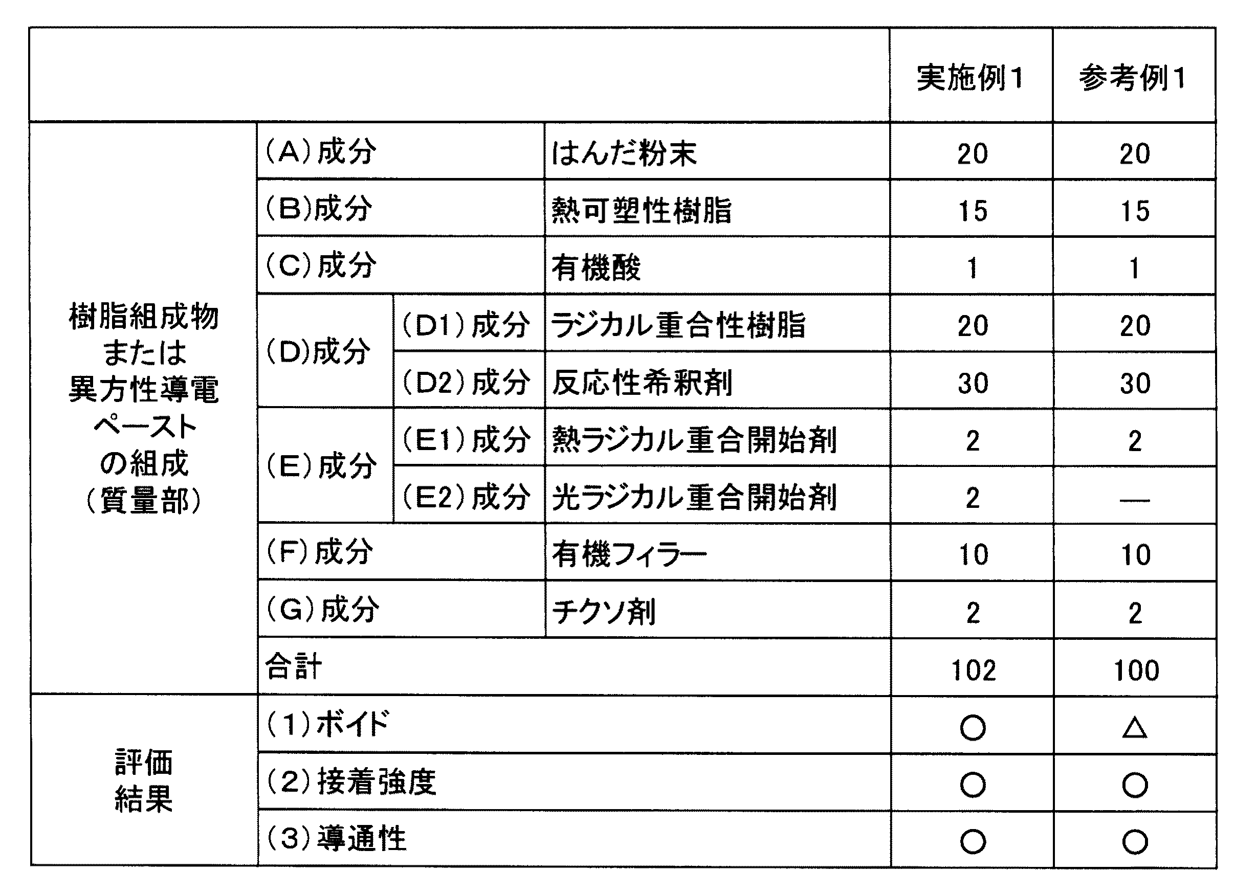
表1に示す結果からも明らかなように、本発明の異方性導電フィルムを用いた場合(実施例1)には、熱圧着時の温度が低温(160℃)の場合にも使用できることが確認された。すなわち、接着強度および導通性については、低温硬化タイプの異方性導電ペーストを用いた場合(参考例1)と同等であった。また、ボイドについては、低温硬化タイプの異方性導電ペーストを用いた場合(参考例1)よりも良好であった。 As is clear from the results shown in Table 1, when the anisotropic conductive film of the present invention is used (Example 1), it can be used even when the temperature at the time of thermocompression bonding is low (160 ° C.). confirmed. That is, the adhesive strength and conductivity were the same as when the low-temperature curing type anisotropic conductive paste was used (Reference Example 1). The voids were better than those in which the low temperature curing type anisotropic conductive paste was used (Reference Example 1).
本発明の異方性導電フィルムの製造方法で得られる異方性導電フィルムは、配線基板同士(例えば、フレキ基板とリジット基板)を接続する技術や、電子部品と配線基板とを接続する技術として好適に用いることができる。 The anisotropic conductive film obtained by the method for producing an anisotropic conductive film of the present invention can be used as a technique for connecting wiring boards (for example, a flexible substrate and a rigid substrate) or a technique for connecting an electronic component and a wiring board. It can be preferably used.
Claims (3)
前記塗布膜に、紫外線を照射する紫外線照射工程と、を備え、
前記(E1)成分が、1,1,3,3−テトラメチルブチルパーオキシ−2−エチルヘキサノエート、およびt−ブチルパーオキシ−2−エチルヘキサノエートからなる群から選択される少なくとも1種であり、
前記(E2)成分が、2−ヒドロキシ−2−メチル−1−フェニルプロパン−1−オン、2−ヒドロキシ−1−〔4−[4−(2−ヒドロキシ−2−メチル−プロピオニル)−ベンジル]−フェニル〕−2−メチル−プロパン−1−オン、および1−ヒドロキシシクロヘキシルフェニルケトンからなる群から選択される少なくとも1種である
ことを特徴とする異方性導電フィルムの製造方法。 (A) solder powder, (B) thermoplastic resin, (C) organic acid, (D) a polymerizable compound having one or more unsaturated double bonds in one molecule, and (E) radical polymerization. A resin composition containing an initiator and the component (E) containing (E1) a thermal radical polymerization initiator and (E2) a photoradical polymerization initiator is applied onto a release film to form a coating film. The coating process to form and
The coating film is provided with an ultraviolet irradiation step of irradiating the coating film with ultraviolet rays .
At least one of the components (E1) selected from the group consisting of 1,1,3,3-tetramethylbutylperoxy-2-ethylhexanoate and t-butylperoxy-2-ethylhexanoate. Seed and
The component (E2) is 2-hydroxy-2-methyl-1-phenylpropan-1-one, 2-hydroxy-1- [4- [4- (2-hydroxy-2-methyl-propionyl) -benzyl]. -Phenyl] A method for producing an anisotropic conductive film, which is at least one selected from the group consisting of -2-methyl-propane-1-one and 1-hydroxycyclohexylphenylketone .
前記塗布膜の厚みが、10μm以上120μm以下である
ことを特徴とする異方性導電フィルムの製造方法。 In the method for producing an anisotropic conductive film according to claim 1,
A method for producing an anisotropic conductive film, wherein the thickness of the coating film is 10 μm or more and 120 μm or less.
前記紫外線照射工程での紫外線の露光量は、10mJ/cm2以上300mJ/cm2以下である
ことを特徴とする異方性導電フィルムの製造方法。 In the method for producing an anisotropic conductive film according to claim 1 or 2.
A method for producing an anisotropic conductive film, wherein the exposure amount of ultraviolet rays in the ultraviolet irradiation step is 10 mJ / cm 2 or more and 300 mJ / cm 2 or less.
Priority Applications (1)
| Application Number | Priority Date | Filing Date | Title |
|---|---|---|---|
| JP2016189386A JP6772012B2 (en) | 2016-09-28 | 2016-09-28 | Method for manufacturing anisotropic conductive film |
Applications Claiming Priority (1)
| Application Number | Priority Date | Filing Date | Title |
|---|---|---|---|
| JP2016189386A JP6772012B2 (en) | 2016-09-28 | 2016-09-28 | Method for manufacturing anisotropic conductive film |
Publications (2)
| Publication Number | Publication Date |
|---|---|
| JP2018053055A JP2018053055A (en) | 2018-04-05 |
| JP6772012B2 true JP6772012B2 (en) | 2020-10-21 |
Family
ID=61835170
Family Applications (1)
| Application Number | Title | Priority Date | Filing Date |
|---|---|---|---|
| JP2016189386A Active JP6772012B2 (en) | 2016-09-28 | 2016-09-28 | Method for manufacturing anisotropic conductive film |
Country Status (1)
| Country | Link |
|---|---|
| JP (1) | JP6772012B2 (en) |
Family Cites Families (7)
| Publication number | Priority date | Publication date | Assignee | Title |
|---|---|---|---|---|
| JPH08325543A (en) * | 1995-06-05 | 1996-12-10 | Soken Chem & Eng Co Ltd | Anisotropically electroconductive adhesive |
| JPH0985489A (en) * | 1995-09-20 | 1997-03-31 | Sony Corp | Solder and soldering method |
| JP3419436B2 (en) * | 1997-12-26 | 2003-06-23 | ソニーケミカル株式会社 | Anisotropic conductive adhesive film |
| JP5540916B2 (en) * | 2010-06-15 | 2014-07-02 | デクセリアルズ株式会社 | Method for manufacturing connection structure |
| JP6061642B2 (en) * | 2012-09-24 | 2017-01-18 | 株式会社タムラ製作所 | Anisotropic conductive paste and printed wiring board using the same |
| JP6068106B2 (en) * | 2012-09-24 | 2017-01-25 | 株式会社タムラ製作所 | Anisotropic conductive paste and printed wiring board using the same |
| JP6435627B2 (en) * | 2014-03-20 | 2018-12-12 | デクセリアルズ株式会社 | Anisotropic conductive film and manufacturing method thereof |
-
2016
- 2016-09-28 JP JP2016189386A patent/JP6772012B2/en active Active
Also Published As
| Publication number | Publication date |
|---|---|
| JP2018053055A (en) | 2018-04-05 |
Similar Documents
| Publication | Publication Date | Title |
|---|---|---|
| JP6293554B2 (en) | Anisotropic conductive paste and method for manufacturing printed wiring board using the same | |
| JP6280981B2 (en) | Anisotropic conductive paste and method for manufacturing printed wiring board using the same | |
| JP6061644B2 (en) | Anisotropic conductive paste and printed wiring board using the same | |
| CA2781958C (en) | Flux for solder paste and solder paste | |
| JP5856747B2 (en) | Soldering flux and solder paste composition | |
| JP5887304B2 (en) | Anisotropic conductive paste and printed wiring board using the same | |
| US20060194920A1 (en) | Thermally conductive adhesive composition and process for device attachment | |
| JP5916376B2 (en) | Adhesive composition and method for connecting solar cell and wiring board using the same | |
| JP6061643B2 (en) | Anisotropic conductive paste and printed wiring board using the same | |
| JP6061642B2 (en) | Anisotropic conductive paste and printed wiring board using the same | |
| JP6230569B2 (en) | Anisotropic conductive adhesive and method for producing printed wiring board using the same | |
| JP6346877B2 (en) | Anisotropic conductive adhesive and method for producing printed wiring board using the same | |
| JP6772012B2 (en) | Method for manufacturing anisotropic conductive film | |
| JP6095639B2 (en) | Anisotropic conductive paste and method for manufacturing printed wiring board using the same | |
| JP6181038B2 (en) | Anisotropic conductive paste and method for manufacturing printed wiring board using the same | |
| JP6148267B2 (en) | Anisotropic conductive paste and method for manufacturing printed wiring board using the same | |
| JP2020164744A (en) | Conductive adhesive and syringe | |
| JP6130422B2 (en) | Electronic component joining method, and solder composition and pretreatment agent used in the method | |
| JP6061645B2 (en) | Anisotropic conductive paste and printed wiring board using the same | |
| JP2018060788A (en) | Conductive adhesive, cured product and electronic component | |
| JP6130417B2 (en) | Electronic component joining method, and solder composition and pretreatment agent used in the method | |
| JP2017069543A (en) | Connection structure and electronic component | |
| JP2002134886A (en) | Soldering flux | |
| JP2016148012A (en) | Curable composition and electronic component |
Legal Events
| Date | Code | Title | Description |
|---|---|---|---|
| A621 | Written request for application examination |
Free format text: JAPANESE INTERMEDIATE CODE: A621 Effective date: 20190709 |
|
| A977 | Report on retrieval |
Free format text: JAPANESE INTERMEDIATE CODE: A971007 Effective date: 20200610 |
|
| A131 | Notification of reasons for refusal |
Free format text: JAPANESE INTERMEDIATE CODE: A131 Effective date: 20200623 |
|
| A521 | Written amendment |
Free format text: JAPANESE INTERMEDIATE CODE: A523 Effective date: 20200722 |
|
| TRDD | Decision of grant or rejection written | ||
| A01 | Written decision to grant a patent or to grant a registration (utility model) |
Free format text: JAPANESE INTERMEDIATE CODE: A01 Effective date: 20200915 |
|
| A61 | First payment of annual fees (during grant procedure) |
Free format text: JAPANESE INTERMEDIATE CODE: A61 Effective date: 20200930 |
|
| R150 | Certificate of patent or registration of utility model |
Ref document number: 6772012 Country of ref document: JP Free format text: JAPANESE INTERMEDIATE CODE: R150 |