JP6705718B2 - Wiring board and manufacturing method thereof - Google Patents
Wiring board and manufacturing method thereof Download PDFInfo
- Publication number
- JP6705718B2 JP6705718B2 JP2016156803A JP2016156803A JP6705718B2 JP 6705718 B2 JP6705718 B2 JP 6705718B2 JP 2016156803 A JP2016156803 A JP 2016156803A JP 2016156803 A JP2016156803 A JP 2016156803A JP 6705718 B2 JP6705718 B2 JP 6705718B2
- Authority
- JP
- Japan
- Prior art keywords
- insulating film
- layer
- wiring
- insulating
- wiring board
- Prior art date
- Legal status (The legal status is an assumption and is not a legal conclusion. Google has not performed a legal analysis and makes no representation as to the accuracy of the status listed.)
- Active
Links
- 238000004519 manufacturing process Methods 0.000 title claims description 44
- 239000010410 layer Substances 0.000 claims description 683
- 239000011347 resin Substances 0.000 claims description 117
- 229920005989 resin Polymers 0.000 claims description 117
- 239000004065 semiconductor Substances 0.000 claims description 101
- 229910000679 solder Inorganic materials 0.000 claims description 99
- 238000000034 method Methods 0.000 claims description 52
- 230000003014 reinforcing effect Effects 0.000 claims description 41
- 230000008569 process Effects 0.000 claims description 18
- 239000012790 adhesive layer Substances 0.000 claims description 8
- 238000010030 laminating Methods 0.000 claims description 8
- 239000000758 substrate Substances 0.000 claims description 6
- 239000011888 foil Substances 0.000 description 57
- 229910052751 metal Inorganic materials 0.000 description 46
- 239000002184 metal Substances 0.000 description 46
- RYGMFSIKBFXOCR-UHFFFAOYSA-N Copper Chemical compound [Cu] RYGMFSIKBFXOCR-UHFFFAOYSA-N 0.000 description 45
- 239000010949 copper Substances 0.000 description 40
- 229910052802 copper Inorganic materials 0.000 description 33
- 239000000463 material Substances 0.000 description 32
- 230000004888 barrier function Effects 0.000 description 30
- 230000004048 modification Effects 0.000 description 28
- 238000012986 modification Methods 0.000 description 28
- PXHVJJICTQNCMI-UHFFFAOYSA-N nickel Substances [Ni] PXHVJJICTQNCMI-UHFFFAOYSA-N 0.000 description 27
- 238000005530 etching Methods 0.000 description 23
- 238000005520 cutting process Methods 0.000 description 15
- 239000000945 filler Substances 0.000 description 15
- 238000007789 sealing Methods 0.000 description 14
- 239000011889 copper foil Substances 0.000 description 13
- 239000004593 Epoxy Substances 0.000 description 11
- 239000003963 antioxidant agent Substances 0.000 description 11
- 230000003078 antioxidant effect Effects 0.000 description 11
- 238000007772 electroless plating Methods 0.000 description 11
- 239000000654 additive Substances 0.000 description 10
- 238000010586 diagram Methods 0.000 description 10
- 238000009413 insulation Methods 0.000 description 10
- 229910052759 nickel Inorganic materials 0.000 description 9
- 229920001187 thermosetting polymer Polymers 0.000 description 9
- 229910045601 alloy Inorganic materials 0.000 description 8
- 239000000956 alloy Substances 0.000 description 8
- 239000003990 capacitor Substances 0.000 description 7
- 238000009713 electroplating Methods 0.000 description 7
- 239000003822 epoxy resin Substances 0.000 description 7
- 229920000647 polyepoxide Polymers 0.000 description 7
- 239000000243 solution Substances 0.000 description 7
- 239000007864 aqueous solution Substances 0.000 description 6
- 239000011521 glass Substances 0.000 description 6
- 238000012545 processing Methods 0.000 description 6
- 238000003672 processing method Methods 0.000 description 6
- 229910052718 tin Inorganic materials 0.000 description 6
- 239000004744 fabric Substances 0.000 description 5
- 230000000149 penetrating effect Effects 0.000 description 5
- XEEYBQQBJWHFJM-UHFFFAOYSA-N Iron Chemical compound [Fe] XEEYBQQBJWHFJM-UHFFFAOYSA-N 0.000 description 4
- VYPSYNLAJGMNEJ-UHFFFAOYSA-N Silicium dioxide Chemical compound O=[Si]=O VYPSYNLAJGMNEJ-UHFFFAOYSA-N 0.000 description 4
- NIXOWILDQLNWCW-UHFFFAOYSA-N acrylic acid group Chemical group C(C=C)(=O)O NIXOWILDQLNWCW-UHFFFAOYSA-N 0.000 description 4
- ROOXNKNUYICQNP-UHFFFAOYSA-N ammonium persulfate Chemical compound [NH4+].[NH4+].[O-]S(=O)(=O)OOS([O-])(=O)=O ROOXNKNUYICQNP-UHFFFAOYSA-N 0.000 description 4
- 230000005012 migration Effects 0.000 description 4
- 238000013508 migration Methods 0.000 description 4
- 239000005011 phenolic resin Substances 0.000 description 4
- 238000007747 plating Methods 0.000 description 4
- 229910052709 silver Inorganic materials 0.000 description 4
- HEMHJVSKTPXQMS-UHFFFAOYSA-M Sodium hydroxide Chemical compound [OH-].[Na+] HEMHJVSKTPXQMS-UHFFFAOYSA-M 0.000 description 3
- -1 azole compound Chemical class 0.000 description 3
- 239000007788 liquid Substances 0.000 description 3
- 238000000206 photolithography Methods 0.000 description 3
- 238000004528 spin coating Methods 0.000 description 3
- VYZAMTAEIAYCRO-UHFFFAOYSA-N Chromium Chemical compound [Cr] VYZAMTAEIAYCRO-UHFFFAOYSA-N 0.000 description 2
- MHAJPDPJQMAIIY-UHFFFAOYSA-N Hydrogen peroxide Chemical compound OO MHAJPDPJQMAIIY-UHFFFAOYSA-N 0.000 description 2
- QAOWNCQODCNURD-UHFFFAOYSA-N Sulfuric acid Chemical compound OS(O)(=O)=O QAOWNCQODCNURD-UHFFFAOYSA-N 0.000 description 2
- 229910001870 ammonium persulfate Inorganic materials 0.000 description 2
- 229920006231 aramid fiber Polymers 0.000 description 2
- 229910052804 chromium Inorganic materials 0.000 description 2
- 239000011651 chromium Substances 0.000 description 2
- ORTQZVOHEJQUHG-UHFFFAOYSA-L copper(II) chloride Chemical compound Cl[Cu]Cl ORTQZVOHEJQUHG-UHFFFAOYSA-L 0.000 description 2
- XLJMAIOERFSOGZ-UHFFFAOYSA-M cyanate Chemical compound [O-]C#N XLJMAIOERFSOGZ-UHFFFAOYSA-M 0.000 description 2
- 238000011161 development Methods 0.000 description 2
- 239000003365 glass fiber Substances 0.000 description 2
- RAXXELZNTBOGNW-UHFFFAOYSA-N imidazole Natural products C1=CNC=N1 RAXXELZNTBOGNW-UHFFFAOYSA-N 0.000 description 2
- 150000003949 imides Chemical class 0.000 description 2
- 229910052742 iron Inorganic materials 0.000 description 2
- 230000001678 irradiating effect Effects 0.000 description 2
- 239000000155 melt Substances 0.000 description 2
- 239000004745 nonwoven fabric Substances 0.000 description 2
- 238000007650 screen-printing Methods 0.000 description 2
- 125000006850 spacer group Chemical group 0.000 description 2
- 238000001721 transfer moulding Methods 0.000 description 2
- 238000001039 wet etching Methods 0.000 description 2
- 239000002759 woven fabric Substances 0.000 description 2
- KAESVJOAVNADME-UHFFFAOYSA-N 1H-pyrrole Natural products C=1C=CNC=1 KAESVJOAVNADME-UHFFFAOYSA-N 0.000 description 1
- LCPVQAHEFVXVKT-UHFFFAOYSA-N 2-(2,4-difluorophenoxy)pyridin-3-amine Chemical compound NC1=CC=CN=C1OC1=CC=C(F)C=C1F LCPVQAHEFVXVKT-UHFFFAOYSA-N 0.000 description 1
- 239000004925 Acrylic resin Substances 0.000 description 1
- 229920000178 Acrylic resin Polymers 0.000 description 1
- 229920000049 Carbon (fiber) Polymers 0.000 description 1
- 229910021578 Iron(III) chloride Inorganic materials 0.000 description 1
- 239000006061 abrasive grain Substances 0.000 description 1
- 230000000996 additive effect Effects 0.000 description 1
- 239000000853 adhesive Substances 0.000 description 1
- 230000001070 adhesive effect Effects 0.000 description 1
- PNEYBMLMFCGWSK-UHFFFAOYSA-N aluminium oxide Inorganic materials [O-2].[O-2].[O-2].[Al+3].[Al+3] PNEYBMLMFCGWSK-UHFFFAOYSA-N 0.000 description 1
- 230000015572 biosynthetic process Effects 0.000 description 1
- 238000005422 blasting Methods 0.000 description 1
- 239000004917 carbon fiber Substances 0.000 description 1
- 230000008859 change Effects 0.000 description 1
- 239000011248 coating agent Substances 0.000 description 1
- 238000000576 coating method Methods 0.000 description 1
- 229960003280 cupric chloride Drugs 0.000 description 1
- 238000000151 deposition Methods 0.000 description 1
- 230000008021 deposition Effects 0.000 description 1
- 230000000994 depressogenic effect Effects 0.000 description 1
- 238000013461 design Methods 0.000 description 1
- 238000005516 engineering process Methods 0.000 description 1
- 239000000835 fiber Substances 0.000 description 1
- 238000010438 heat treatment Methods 0.000 description 1
- 230000006872 improvement Effects 0.000 description 1
- RBTARNINKXHZNM-UHFFFAOYSA-K iron trichloride Chemical compound Cl[Fe](Cl)Cl RBTARNINKXHZNM-UHFFFAOYSA-K 0.000 description 1
- VNWKTOKETHGBQD-UHFFFAOYSA-N methane Chemical compound C VNWKTOKETHGBQD-UHFFFAOYSA-N 0.000 description 1
- 239000000203 mixture Substances 0.000 description 1
- 238000000059 patterning Methods 0.000 description 1
- 238000005498 polishing Methods 0.000 description 1
- 229920001721 polyimide Polymers 0.000 description 1
- 239000003755 preservative agent Substances 0.000 description 1
- 230000002335 preservative effect Effects 0.000 description 1
- 238000003825 pressing Methods 0.000 description 1
- 239000011241 protective layer Substances 0.000 description 1
- 238000000926 separation method Methods 0.000 description 1
- 229910052710 silicon Inorganic materials 0.000 description 1
- 239000010703 silicon Substances 0.000 description 1
- 229920002050 silicone resin Polymers 0.000 description 1
- CHQMHPLRPQMAMX-UHFFFAOYSA-L sodium persulfate Substances [Na+].[Na+].[O-]S(=O)(=O)OOS([O-])(=O)=O CHQMHPLRPQMAMX-UHFFFAOYSA-L 0.000 description 1
- 239000000126 substance Substances 0.000 description 1
- 238000006467 substitution reaction Methods 0.000 description 1
- 239000002335 surface treatment layer Substances 0.000 description 1
Images


Classifications
-
- H—ELECTRICITY
- H01—ELECTRIC ELEMENTS
- H01L—SEMICONDUCTOR DEVICES NOT COVERED BY CLASS H10
- H01L23/00—Details of semiconductor or other solid state devices
- H01L23/48—Arrangements for conducting electric current to or from the solid state body in operation, e.g. leads, terminal arrangements ; Selection of materials therefor
- H01L23/488—Arrangements for conducting electric current to or from the solid state body in operation, e.g. leads, terminal arrangements ; Selection of materials therefor consisting of soldered or bonded constructions
- H01L23/498—Leads, i.e. metallisations or lead-frames on insulating substrates, e.g. chip carriers
- H01L23/49822—Multilayer substrates
-
- H—ELECTRICITY
- H01—ELECTRIC ELEMENTS
- H01L—SEMICONDUCTOR DEVICES NOT COVERED BY CLASS H10
- H01L21/00—Processes or apparatus adapted for the manufacture or treatment of semiconductor or solid state devices or of parts thereof
- H01L21/02—Manufacture or treatment of semiconductor devices or of parts thereof
- H01L21/04—Manufacture or treatment of semiconductor devices or of parts thereof the devices having potential barriers, e.g. a PN junction, depletion layer or carrier concentration layer
- H01L21/48—Manufacture or treatment of parts, e.g. containers, prior to assembly of the devices, using processes not provided for in a single one of the subgroups H01L21/06 - H01L21/326
- H01L21/4814—Conductive parts
- H01L21/4846—Leads on or in insulating or insulated substrates, e.g. metallisation
- H01L21/4857—Multilayer substrates
-
- H—ELECTRICITY
- H01—ELECTRIC ELEMENTS
- H01L—SEMICONDUCTOR DEVICES NOT COVERED BY CLASS H10
- H01L23/00—Details of semiconductor or other solid state devices
- H01L23/16—Fillings or auxiliary members in containers or encapsulations, e.g. centering rings
-
- H—ELECTRICITY
- H01—ELECTRIC ELEMENTS
- H01L—SEMICONDUCTOR DEVICES NOT COVERED BY CLASS H10
- H01L21/00—Processes or apparatus adapted for the manufacture or treatment of semiconductor or solid state devices or of parts thereof
- H01L21/02—Manufacture or treatment of semiconductor devices or of parts thereof
- H01L21/04—Manufacture or treatment of semiconductor devices or of parts thereof the devices having potential barriers, e.g. a PN junction, depletion layer or carrier concentration layer
- H01L21/50—Assembly of semiconductor devices using processes or apparatus not provided for in a single one of the subgroups H01L21/06 - H01L21/326, e.g. sealing of a cap to a base of a container
- H01L21/56—Encapsulations, e.g. encapsulation layers, coatings
- H01L21/561—Batch processing
-
- H—ELECTRICITY
- H01—ELECTRIC ELEMENTS
- H01L—SEMICONDUCTOR DEVICES NOT COVERED BY CLASS H10
- H01L21/00—Processes or apparatus adapted for the manufacture or treatment of semiconductor or solid state devices or of parts thereof
- H01L21/02—Manufacture or treatment of semiconductor devices or of parts thereof
- H01L21/04—Manufacture or treatment of semiconductor devices or of parts thereof the devices having potential barriers, e.g. a PN junction, depletion layer or carrier concentration layer
- H01L21/50—Assembly of semiconductor devices using processes or apparatus not provided for in a single one of the subgroups H01L21/06 - H01L21/326, e.g. sealing of a cap to a base of a container
- H01L21/56—Encapsulations, e.g. encapsulation layers, coatings
- H01L21/568—Temporary substrate used as encapsulation process aid
-
- H—ELECTRICITY
- H01—ELECTRIC ELEMENTS
- H01L—SEMICONDUCTOR DEVICES NOT COVERED BY CLASS H10
- H01L2224/00—Indexing scheme for arrangements for connecting or disconnecting semiconductor or solid-state bodies and methods related thereto as covered by H01L24/00
- H01L2224/01—Means for bonding being attached to, or being formed on, the surface to be connected, e.g. chip-to-package, die-attach, "first-level" interconnects; Manufacturing methods related thereto
- H01L2224/10—Bump connectors; Manufacturing methods related thereto
- H01L2224/12—Structure, shape, material or disposition of the bump connectors prior to the connecting process
- H01L2224/13—Structure, shape, material or disposition of the bump connectors prior to the connecting process of an individual bump connector
- H01L2224/13001—Core members of the bump connector
- H01L2224/13099—Material
- H01L2224/131—Material with a principal constituent of the material being a metal or a metalloid, e.g. boron [B], silicon [Si], germanium [Ge], arsenic [As], antimony [Sb], tellurium [Te] and polonium [Po], and alloys thereof
- H01L2224/13101—Material with a principal constituent of the material being a metal or a metalloid, e.g. boron [B], silicon [Si], germanium [Ge], arsenic [As], antimony [Sb], tellurium [Te] and polonium [Po], and alloys thereof the principal constituent melting at a temperature of less than 400°C
- H01L2224/13111—Tin [Sn] as principal constituent
-
- H—ELECTRICITY
- H01—ELECTRIC ELEMENTS
- H01L—SEMICONDUCTOR DEVICES NOT COVERED BY CLASS H10
- H01L2224/00—Indexing scheme for arrangements for connecting or disconnecting semiconductor or solid-state bodies and methods related thereto as covered by H01L24/00
- H01L2224/01—Means for bonding being attached to, or being formed on, the surface to be connected, e.g. chip-to-package, die-attach, "first-level" interconnects; Manufacturing methods related thereto
- H01L2224/10—Bump connectors; Manufacturing methods related thereto
- H01L2224/12—Structure, shape, material or disposition of the bump connectors prior to the connecting process
- H01L2224/13—Structure, shape, material or disposition of the bump connectors prior to the connecting process of an individual bump connector
- H01L2224/13001—Core members of the bump connector
- H01L2224/13099—Material
- H01L2224/131—Material with a principal constituent of the material being a metal or a metalloid, e.g. boron [B], silicon [Si], germanium [Ge], arsenic [As], antimony [Sb], tellurium [Te] and polonium [Po], and alloys thereof
- H01L2224/13101—Material with a principal constituent of the material being a metal or a metalloid, e.g. boron [B], silicon [Si], germanium [Ge], arsenic [As], antimony [Sb], tellurium [Te] and polonium [Po], and alloys thereof the principal constituent melting at a temperature of less than 400°C
- H01L2224/13116—Lead [Pb] as principal constituent
-
- H—ELECTRICITY
- H01—ELECTRIC ELEMENTS
- H01L—SEMICONDUCTOR DEVICES NOT COVERED BY CLASS H10
- H01L2224/00—Indexing scheme for arrangements for connecting or disconnecting semiconductor or solid-state bodies and methods related thereto as covered by H01L24/00
- H01L2224/01—Means for bonding being attached to, or being formed on, the surface to be connected, e.g. chip-to-package, die-attach, "first-level" interconnects; Manufacturing methods related thereto
- H01L2224/10—Bump connectors; Manufacturing methods related thereto
- H01L2224/15—Structure, shape, material or disposition of the bump connectors after the connecting process
- H01L2224/16—Structure, shape, material or disposition of the bump connectors after the connecting process of an individual bump connector
- H01L2224/161—Disposition
- H01L2224/16151—Disposition the bump connector connecting between a semiconductor or solid-state body and an item not being a semiconductor or solid-state body, e.g. chip-to-substrate, chip-to-passive
- H01L2224/16221—Disposition the bump connector connecting between a semiconductor or solid-state body and an item not being a semiconductor or solid-state body, e.g. chip-to-substrate, chip-to-passive the body and the item being stacked
- H01L2224/16225—Disposition the bump connector connecting between a semiconductor or solid-state body and an item not being a semiconductor or solid-state body, e.g. chip-to-substrate, chip-to-passive the body and the item being stacked the item being non-metallic, e.g. insulating substrate with or without metallisation
- H01L2224/16227—Disposition the bump connector connecting between a semiconductor or solid-state body and an item not being a semiconductor or solid-state body, e.g. chip-to-substrate, chip-to-passive the body and the item being stacked the item being non-metallic, e.g. insulating substrate with or without metallisation the bump connector connecting to a bond pad of the item
-
- H—ELECTRICITY
- H01—ELECTRIC ELEMENTS
- H01L—SEMICONDUCTOR DEVICES NOT COVERED BY CLASS H10
- H01L2224/00—Indexing scheme for arrangements for connecting or disconnecting semiconductor or solid-state bodies and methods related thereto as covered by H01L24/00
- H01L2224/01—Means for bonding being attached to, or being formed on, the surface to be connected, e.g. chip-to-package, die-attach, "first-level" interconnects; Manufacturing methods related thereto
- H01L2224/10—Bump connectors; Manufacturing methods related thereto
- H01L2224/15—Structure, shape, material or disposition of the bump connectors after the connecting process
- H01L2224/16—Structure, shape, material or disposition of the bump connectors after the connecting process of an individual bump connector
- H01L2224/161—Disposition
- H01L2224/16151—Disposition the bump connector connecting between a semiconductor or solid-state body and an item not being a semiconductor or solid-state body, e.g. chip-to-substrate, chip-to-passive
- H01L2224/16221—Disposition the bump connector connecting between a semiconductor or solid-state body and an item not being a semiconductor or solid-state body, e.g. chip-to-substrate, chip-to-passive the body and the item being stacked
- H01L2224/16225—Disposition the bump connector connecting between a semiconductor or solid-state body and an item not being a semiconductor or solid-state body, e.g. chip-to-substrate, chip-to-passive the body and the item being stacked the item being non-metallic, e.g. insulating substrate with or without metallisation
- H01L2224/16238—Disposition the bump connector connecting between a semiconductor or solid-state body and an item not being a semiconductor or solid-state body, e.g. chip-to-substrate, chip-to-passive the body and the item being stacked the item being non-metallic, e.g. insulating substrate with or without metallisation the bump connector connecting to a bonding area protruding from the surface of the item
-
- H—ELECTRICITY
- H01—ELECTRIC ELEMENTS
- H01L—SEMICONDUCTOR DEVICES NOT COVERED BY CLASS H10
- H01L2224/00—Indexing scheme for arrangements for connecting or disconnecting semiconductor or solid-state bodies and methods related thereto as covered by H01L24/00
- H01L2224/01—Means for bonding being attached to, or being formed on, the surface to be connected, e.g. chip-to-package, die-attach, "first-level" interconnects; Manufacturing methods related thereto
- H01L2224/26—Layer connectors, e.g. plate connectors, solder or adhesive layers; Manufacturing methods related thereto
- H01L2224/2612—Auxiliary members for layer connectors, e.g. spacers
- H01L2224/26152—Auxiliary members for layer connectors, e.g. spacers being formed on an item to be connected not being a semiconductor or solid-state body
- H01L2224/26175—Flow barriers
-
- H—ELECTRICITY
- H01—ELECTRIC ELEMENTS
- H01L—SEMICONDUCTOR DEVICES NOT COVERED BY CLASS H10
- H01L2224/00—Indexing scheme for arrangements for connecting or disconnecting semiconductor or solid-state bodies and methods related thereto as covered by H01L24/00
- H01L2224/01—Means for bonding being attached to, or being formed on, the surface to be connected, e.g. chip-to-package, die-attach, "first-level" interconnects; Manufacturing methods related thereto
- H01L2224/26—Layer connectors, e.g. plate connectors, solder or adhesive layers; Manufacturing methods related thereto
- H01L2224/31—Structure, shape, material or disposition of the layer connectors after the connecting process
- H01L2224/32—Structure, shape, material or disposition of the layer connectors after the connecting process of an individual layer connector
- H01L2224/321—Disposition
- H01L2224/32151—Disposition the layer connector connecting between a semiconductor or solid-state body and an item not being a semiconductor or solid-state body, e.g. chip-to-substrate, chip-to-passive
- H01L2224/32221—Disposition the layer connector connecting between a semiconductor or solid-state body and an item not being a semiconductor or solid-state body, e.g. chip-to-substrate, chip-to-passive the body and the item being stacked
- H01L2224/32225—Disposition the layer connector connecting between a semiconductor or solid-state body and an item not being a semiconductor or solid-state body, e.g. chip-to-substrate, chip-to-passive the body and the item being stacked the item being non-metallic, e.g. insulating substrate with or without metallisation
-
- H—ELECTRICITY
- H01—ELECTRIC ELEMENTS
- H01L—SEMICONDUCTOR DEVICES NOT COVERED BY CLASS H10
- H01L2224/00—Indexing scheme for arrangements for connecting or disconnecting semiconductor or solid-state bodies and methods related thereto as covered by H01L24/00
- H01L2224/73—Means for bonding being of different types provided for in two or more of groups H01L2224/10, H01L2224/18, H01L2224/26, H01L2224/34, H01L2224/42, H01L2224/50, H01L2224/63, H01L2224/71
- H01L2224/732—Location after the connecting process
- H01L2224/73201—Location after the connecting process on the same surface
- H01L2224/73203—Bump and layer connectors
- H01L2224/73204—Bump and layer connectors the bump connector being embedded into the layer connector
-
- H—ELECTRICITY
- H01—ELECTRIC ELEMENTS
- H01L—SEMICONDUCTOR DEVICES NOT COVERED BY CLASS H10
- H01L2224/00—Indexing scheme for arrangements for connecting or disconnecting semiconductor or solid-state bodies and methods related thereto as covered by H01L24/00
- H01L2224/80—Methods for connecting semiconductor or other solid state bodies using means for bonding being attached to, or being formed on, the surface to be connected
- H01L2224/81—Methods for connecting semiconductor or other solid state bodies using means for bonding being attached to, or being formed on, the surface to be connected using a bump connector
- H01L2224/81001—Methods for connecting semiconductor or other solid state bodies using means for bonding being attached to, or being formed on, the surface to be connected using a bump connector involving a temporary auxiliary member not forming part of the bonding apparatus
- H01L2224/81005—Methods for connecting semiconductor or other solid state bodies using means for bonding being attached to, or being formed on, the surface to be connected using a bump connector involving a temporary auxiliary member not forming part of the bonding apparatus being a temporary or sacrificial substrate
-
- H—ELECTRICITY
- H01—ELECTRIC ELEMENTS
- H01L—SEMICONDUCTOR DEVICES NOT COVERED BY CLASS H10
- H01L2224/00—Indexing scheme for arrangements for connecting or disconnecting semiconductor or solid-state bodies and methods related thereto as covered by H01L24/00
- H01L2224/80—Methods for connecting semiconductor or other solid state bodies using means for bonding being attached to, or being formed on, the surface to be connected
- H01L2224/83—Methods for connecting semiconductor or other solid state bodies using means for bonding being attached to, or being formed on, the surface to be connected using a layer connector
- H01L2224/83001—Methods for connecting semiconductor or other solid state bodies using means for bonding being attached to, or being formed on, the surface to be connected using a layer connector involving a temporary auxiliary member not forming part of the bonding apparatus
- H01L2224/83005—Methods for connecting semiconductor or other solid state bodies using means for bonding being attached to, or being formed on, the surface to be connected using a layer connector involving a temporary auxiliary member not forming part of the bonding apparatus being a temporary or sacrificial substrate
-
- H—ELECTRICITY
- H01—ELECTRIC ELEMENTS
- H01L—SEMICONDUCTOR DEVICES NOT COVERED BY CLASS H10
- H01L2224/00—Indexing scheme for arrangements for connecting or disconnecting semiconductor or solid-state bodies and methods related thereto as covered by H01L24/00
- H01L2224/91—Methods for connecting semiconductor or solid state bodies including different methods provided for in two or more of groups H01L2224/80 - H01L2224/90
- H01L2224/92—Specific sequence of method steps
- H01L2224/921—Connecting a surface with connectors of different types
- H01L2224/9212—Sequential connecting processes
- H01L2224/92122—Sequential connecting processes the first connecting process involving a bump connector
- H01L2224/92125—Sequential connecting processes the first connecting process involving a bump connector the second connecting process involving a layer connector
-
- H—ELECTRICITY
- H01—ELECTRIC ELEMENTS
- H01L—SEMICONDUCTOR DEVICES NOT COVERED BY CLASS H10
- H01L2224/00—Indexing scheme for arrangements for connecting or disconnecting semiconductor or solid-state bodies and methods related thereto as covered by H01L24/00
- H01L2224/93—Batch processes
- H01L2224/95—Batch processes at chip-level, i.e. with connecting carried out on a plurality of singulated devices, i.e. on diced chips
- H01L2224/97—Batch processes at chip-level, i.e. with connecting carried out on a plurality of singulated devices, i.e. on diced chips the devices being connected to a common substrate, e.g. interposer, said common substrate being separable into individual assemblies after connecting
-
- H—ELECTRICITY
- H01—ELECTRIC ELEMENTS
- H01L—SEMICONDUCTOR DEVICES NOT COVERED BY CLASS H10
- H01L2225/00—Details relating to assemblies covered by the group H01L25/00 but not provided for in its subgroups
- H01L2225/03—All the devices being of a type provided for in the same subgroup of groups H01L27/00 - H01L33/648 and H10K99/00
- H01L2225/10—All the devices being of a type provided for in the same subgroup of groups H01L27/00 - H01L33/648 and H10K99/00 the devices having separate containers
- H01L2225/1005—All the devices being of a type provided for in the same subgroup of groups H01L27/00 - H01L33/648 and H10K99/00 the devices having separate containers the devices being of a type provided for in group H01L27/00
- H01L2225/1011—All the devices being of a type provided for in the same subgroup of groups H01L27/00 - H01L33/648 and H10K99/00 the devices having separate containers the devices being of a type provided for in group H01L27/00 the containers being in a stacked arrangement
- H01L2225/1017—All the devices being of a type provided for in the same subgroup of groups H01L27/00 - H01L33/648 and H10K99/00 the devices having separate containers the devices being of a type provided for in group H01L27/00 the containers being in a stacked arrangement the lowermost container comprising a device support
- H01L2225/1023—All the devices being of a type provided for in the same subgroup of groups H01L27/00 - H01L33/648 and H10K99/00 the devices having separate containers the devices being of a type provided for in group H01L27/00 the containers being in a stacked arrangement the lowermost container comprising a device support the support being an insulating substrate
-
- H—ELECTRICITY
- H01—ELECTRIC ELEMENTS
- H01L—SEMICONDUCTOR DEVICES NOT COVERED BY CLASS H10
- H01L2225/00—Details relating to assemblies covered by the group H01L25/00 but not provided for in its subgroups
- H01L2225/03—All the devices being of a type provided for in the same subgroup of groups H01L27/00 - H01L33/648 and H10K99/00
- H01L2225/10—All the devices being of a type provided for in the same subgroup of groups H01L27/00 - H01L33/648 and H10K99/00 the devices having separate containers
- H01L2225/1005—All the devices being of a type provided for in the same subgroup of groups H01L27/00 - H01L33/648 and H10K99/00 the devices having separate containers the devices being of a type provided for in group H01L27/00
- H01L2225/1011—All the devices being of a type provided for in the same subgroup of groups H01L27/00 - H01L33/648 and H10K99/00 the devices having separate containers the devices being of a type provided for in group H01L27/00 the containers being in a stacked arrangement
- H01L2225/1047—Details of electrical connections between containers
- H01L2225/1058—Bump or bump-like electrical connections, e.g. balls, pillars, posts
-
- H—ELECTRICITY
- H01—ELECTRIC ELEMENTS
- H01L—SEMICONDUCTOR DEVICES NOT COVERED BY CLASS H10
- H01L23/00—Details of semiconductor or other solid state devices
- H01L23/12—Mountings, e.g. non-detachable insulating substrates
- H01L23/14—Mountings, e.g. non-detachable insulating substrates characterised by the material or its electrical properties
- H01L23/145—Organic substrates, e.g. plastic
-
- H—ELECTRICITY
- H01—ELECTRIC ELEMENTS
- H01L—SEMICONDUCTOR DEVICES NOT COVERED BY CLASS H10
- H01L23/00—Details of semiconductor or other solid state devices
- H01L23/28—Encapsulations, e.g. encapsulating layers, coatings, e.g. for protection
- H01L23/31—Encapsulations, e.g. encapsulating layers, coatings, e.g. for protection characterised by the arrangement or shape
- H01L23/3107—Encapsulations, e.g. encapsulating layers, coatings, e.g. for protection characterised by the arrangement or shape the device being completely enclosed
- H01L23/3121—Encapsulations, e.g. encapsulating layers, coatings, e.g. for protection characterised by the arrangement or shape the device being completely enclosed a substrate forming part of the encapsulation
- H01L23/3128—Encapsulations, e.g. encapsulating layers, coatings, e.g. for protection characterised by the arrangement or shape the device being completely enclosed a substrate forming part of the encapsulation the substrate having spherical bumps for external connection
-
- H—ELECTRICITY
- H01—ELECTRIC ELEMENTS
- H01L—SEMICONDUCTOR DEVICES NOT COVERED BY CLASS H10
- H01L23/00—Details of semiconductor or other solid state devices
- H01L23/48—Arrangements for conducting electric current to or from the solid state body in operation, e.g. leads, terminal arrangements ; Selection of materials therefor
- H01L23/488—Arrangements for conducting electric current to or from the solid state body in operation, e.g. leads, terminal arrangements ; Selection of materials therefor consisting of soldered or bonded constructions
- H01L23/498—Leads, i.e. metallisations or lead-frames on insulating substrates, e.g. chip carriers
- H01L23/49811—Additional leads joined to the metallisation on the insulating substrate, e.g. pins, bumps, wires, flat leads
- H01L23/49816—Spherical bumps on the substrate for external connection, e.g. ball grid arrays [BGA]
-
- H—ELECTRICITY
- H01—ELECTRIC ELEMENTS
- H01L—SEMICONDUCTOR DEVICES NOT COVERED BY CLASS H10
- H01L23/00—Details of semiconductor or other solid state devices
- H01L23/48—Arrangements for conducting electric current to or from the solid state body in operation, e.g. leads, terminal arrangements ; Selection of materials therefor
- H01L23/488—Arrangements for conducting electric current to or from the solid state body in operation, e.g. leads, terminal arrangements ; Selection of materials therefor consisting of soldered or bonded constructions
- H01L23/498—Leads, i.e. metallisations or lead-frames on insulating substrates, e.g. chip carriers
- H01L23/49827—Via connections through the substrates, e.g. pins going through the substrate, coaxial cables
-
- H—ELECTRICITY
- H01—ELECTRIC ELEMENTS
- H01L—SEMICONDUCTOR DEVICES NOT COVERED BY CLASS H10
- H01L23/00—Details of semiconductor or other solid state devices
- H01L23/52—Arrangements for conducting electric current within the device in operation from one component to another, i.e. interconnections, e.g. wires, lead frames
- H01L23/538—Arrangements for conducting electric current within the device in operation from one component to another, i.e. interconnections, e.g. wires, lead frames the interconnection structure between a plurality of semiconductor chips being formed on, or in, insulating substrates
- H01L23/5389—Arrangements for conducting electric current within the device in operation from one component to another, i.e. interconnections, e.g. wires, lead frames the interconnection structure between a plurality of semiconductor chips being formed on, or in, insulating substrates the chips being integrally enclosed by the interconnect and support structures
-
- H—ELECTRICITY
- H01—ELECTRIC ELEMENTS
- H01L—SEMICONDUCTOR DEVICES NOT COVERED BY CLASS H10
- H01L24/00—Arrangements for connecting or disconnecting semiconductor or solid-state bodies; Methods or apparatus related thereto
- H01L24/01—Means for bonding being attached to, or being formed on, the surface to be connected, e.g. chip-to-package, die-attach, "first-level" interconnects; Manufacturing methods related thereto
- H01L24/10—Bump connectors ; Manufacturing methods related thereto
- H01L24/12—Structure, shape, material or disposition of the bump connectors prior to the connecting process
- H01L24/13—Structure, shape, material or disposition of the bump connectors prior to the connecting process of an individual bump connector
-
- H—ELECTRICITY
- H01—ELECTRIC ELEMENTS
- H01L—SEMICONDUCTOR DEVICES NOT COVERED BY CLASS H10
- H01L24/00—Arrangements for connecting or disconnecting semiconductor or solid-state bodies; Methods or apparatus related thereto
- H01L24/01—Means for bonding being attached to, or being formed on, the surface to be connected, e.g. chip-to-package, die-attach, "first-level" interconnects; Manufacturing methods related thereto
- H01L24/10—Bump connectors ; Manufacturing methods related thereto
- H01L24/15—Structure, shape, material or disposition of the bump connectors after the connecting process
- H01L24/16—Structure, shape, material or disposition of the bump connectors after the connecting process of an individual bump connector
-
- H—ELECTRICITY
- H01—ELECTRIC ELEMENTS
- H01L—SEMICONDUCTOR DEVICES NOT COVERED BY CLASS H10
- H01L24/00—Arrangements for connecting or disconnecting semiconductor or solid-state bodies; Methods or apparatus related thereto
- H01L24/80—Methods for connecting semiconductor or other solid state bodies using means for bonding being attached to, or being formed on, the surface to be connected
- H01L24/81—Methods for connecting semiconductor or other solid state bodies using means for bonding being attached to, or being formed on, the surface to be connected using a bump connector
-
- H—ELECTRICITY
- H01—ELECTRIC ELEMENTS
- H01L—SEMICONDUCTOR DEVICES NOT COVERED BY CLASS H10
- H01L24/00—Arrangements for connecting or disconnecting semiconductor or solid-state bodies; Methods or apparatus related thereto
- H01L24/80—Methods for connecting semiconductor or other solid state bodies using means for bonding being attached to, or being formed on, the surface to be connected
- H01L24/83—Methods for connecting semiconductor or other solid state bodies using means for bonding being attached to, or being formed on, the surface to be connected using a layer connector
-
- H—ELECTRICITY
- H01—ELECTRIC ELEMENTS
- H01L—SEMICONDUCTOR DEVICES NOT COVERED BY CLASS H10
- H01L24/00—Arrangements for connecting or disconnecting semiconductor or solid-state bodies; Methods or apparatus related thereto
- H01L24/91—Methods for connecting semiconductor or solid state bodies including different methods provided for in two or more of groups H01L24/80 - H01L24/90
- H01L24/92—Specific sequence of method steps
-
- H—ELECTRICITY
- H01—ELECTRIC ELEMENTS
- H01L—SEMICONDUCTOR DEVICES NOT COVERED BY CLASS H10
- H01L24/00—Arrangements for connecting or disconnecting semiconductor or solid-state bodies; Methods or apparatus related thereto
- H01L24/93—Batch processes
- H01L24/95—Batch processes at chip-level, i.e. with connecting carried out on a plurality of singulated devices, i.e. on diced chips
- H01L24/97—Batch processes at chip-level, i.e. with connecting carried out on a plurality of singulated devices, i.e. on diced chips the devices being connected to a common substrate, e.g. interposer, said common substrate being separable into individual assemblies after connecting
-
- H—ELECTRICITY
- H01—ELECTRIC ELEMENTS
- H01L—SEMICONDUCTOR DEVICES NOT COVERED BY CLASS H10
- H01L2924/00—Indexing scheme for arrangements or methods for connecting or disconnecting semiconductor or solid-state bodies as covered by H01L24/00
- H01L2924/15—Details of package parts other than the semiconductor or other solid state devices to be connected
- H01L2924/151—Die mounting substrate
- H01L2924/153—Connection portion
- H01L2924/1531—Connection portion the connection portion being formed only on the surface of the substrate opposite to the die mounting surface
- H01L2924/15311—Connection portion the connection portion being formed only on the surface of the substrate opposite to the die mounting surface being a ball array, e.g. BGA
-
- H—ELECTRICITY
- H01—ELECTRIC ELEMENTS
- H01L—SEMICONDUCTOR DEVICES NOT COVERED BY CLASS H10
- H01L2924/00—Indexing scheme for arrangements or methods for connecting or disconnecting semiconductor or solid-state bodies as covered by H01L24/00
- H01L2924/15—Details of package parts other than the semiconductor or other solid state devices to be connected
- H01L2924/151—Die mounting substrate
- H01L2924/153—Connection portion
- H01L2924/1532—Connection portion the connection portion being formed on the die mounting surface of the substrate
- H01L2924/1533—Connection portion the connection portion being formed on the die mounting surface of the substrate the connection portion being formed both on the die mounting surface of the substrate and outside the die mounting surface of the substrate
- H01L2924/15331—Connection portion the connection portion being formed on the die mounting surface of the substrate the connection portion being formed both on the die mounting surface of the substrate and outside the die mounting surface of the substrate being a ball array, e.g. BGA
-
- H—ELECTRICITY
- H01—ELECTRIC ELEMENTS
- H01L—SEMICONDUCTOR DEVICES NOT COVERED BY CLASS H10
- H01L2924/00—Indexing scheme for arrangements or methods for connecting or disconnecting semiconductor or solid-state bodies as covered by H01L24/00
- H01L2924/19—Details of hybrid assemblies other than the semiconductor or other solid state devices to be connected
- H01L2924/1901—Structure
- H01L2924/1904—Component type
- H01L2924/19041—Component type being a capacitor
-
- H—ELECTRICITY
- H01—ELECTRIC ELEMENTS
- H01L—SEMICONDUCTOR DEVICES NOT COVERED BY CLASS H10
- H01L2924/00—Indexing scheme for arrangements or methods for connecting or disconnecting semiconductor or solid-state bodies as covered by H01L24/00
- H01L2924/19—Details of hybrid assemblies other than the semiconductor or other solid state devices to be connected
- H01L2924/191—Disposition
- H01L2924/19101—Disposition of discrete passive components
- H01L2924/19105—Disposition of discrete passive components in a side-by-side arrangement on a common die mounting substrate
-
- H—ELECTRICITY
- H01—ELECTRIC ELEMENTS
- H01L—SEMICONDUCTOR DEVICES NOT COVERED BY CLASS H10
- H01L2924/00—Indexing scheme for arrangements or methods for connecting or disconnecting semiconductor or solid-state bodies as covered by H01L24/00
- H01L2924/30—Technical effects
- H01L2924/35—Mechanical effects
- H01L2924/351—Thermal stress
- H01L2924/3511—Warping
Landscapes
- Engineering & Computer Science (AREA)
- Physics & Mathematics (AREA)
- Condensed Matter Physics & Semiconductors (AREA)
- General Physics & Mathematics (AREA)
- Computer Hardware Design (AREA)
- Microelectronics & Electronic Packaging (AREA)
- Power Engineering (AREA)
- Ceramic Engineering (AREA)
- Manufacturing & Machinery (AREA)
- Production Of Multi-Layered Print Wiring Board (AREA)
Description
本発明は、配線基板及びその製造方法に関する。 The present invention relates to a wiring board and a method for manufacturing the same.
従来、配線層と絶縁層とが交互に積層され、配線層同士が絶縁層を貫通するビアホールを介して接続された所謂ビルドアップ配線基板が知られている。このような配線基板において、絶縁層が補強部材を有していない場合には、配線基板としての強度が弱くなるおそれがある。そのため、最外の絶縁層として、補強部材に絶縁性樹脂を含浸させた所謂プリプレグを用い、配線基板としての強度を確保している(例えば、特許文献1参照)。 Conventionally, there is known a so-called build-up wiring board in which wiring layers and insulating layers are alternately laminated, and the wiring layers are connected to each other through via holes penetrating the insulating layers. In such a wiring board, if the insulating layer does not have a reinforcing member, the strength of the wiring board may be weakened. Therefore, a so-called prepreg in which a reinforcing member is impregnated with an insulating resin is used as the outermost insulating layer to secure the strength as a wiring board (see, for example, Patent Document 1).
しかしながら、絶縁層としてプリプレグを用いると、最外の絶縁層を薄くした場合に、ガラスクロス等の補強部材が最外の絶縁層に埋め込まれた配線層と接触し、絶縁信頼性を低下させる問題があった。 However, when prepreg is used as the insulating layer, when the outermost insulating layer is thinned, a reinforcing member such as glass cloth comes into contact with the wiring layer embedded in the outermost insulating layer, which lowers the insulation reliability. was there.
又、プリプレグは溶融粘度が高く樹脂の埋め込み性が十分ではないため、最外の絶縁層に埋め込まれた配線層が微細な場合には、配線層間に樹脂が十分に埋め込まれずにボイド等が発生し、絶縁信頼性を低下させる問題があった。 Also, since the prepreg has a high melt viscosity and the resin embeddability is not sufficient, when the wiring layer embedded in the outermost insulating layer is fine, the resin is not sufficiently embedded between the wiring layers and voids or the like occur. However, there is a problem that insulation reliability is reduced.
本発明は、上記の点に鑑みてなされたものであり、強度を確保すると共に絶縁信頼性を向上させた配線基板を提供することを課題とする。 The present invention has been made in view of the above points, and an object of the present invention is to provide a wiring board that secures strength and improves insulation reliability.
本配線基板は、第1絶縁膜の一方の面に第2絶縁膜が積層され、前記第1絶縁膜の他方の面が外部に露出する絶縁層と、前記第1絶縁膜に埋め込まれ、所定面が前記第1絶縁膜の他方の面から露出する第1配線層と、を有し、前記絶縁層は、前記第1絶縁膜及び前記第2絶縁膜を貫通し、前記第1配線層の前記所定面の反対面を露出する開口部を備え、前記開口部の前記第1絶縁膜に形成された部分に、前記開口部の内壁を前記第1絶縁膜側に後退させる凹部が形成され、前記開口部の前記第2絶縁膜に形成された部分は、前記凹部と連通する部分で径が最小となる逆円錐台形状であり、前記第1絶縁膜は前記第2絶縁膜よりもエッチングされやすく、前記第1絶縁膜は、前記第1配線層の側面と、前記所定面の反対面を被覆し、前記第1絶縁膜は樹脂のみから構成され、前記第2絶縁膜は補強部材に樹脂を含浸させた構成とされていることを要件とする。 In the wiring board, the second insulating film is laminated on one surface of the first insulating film, the other surface of the first insulating film is exposed to the outside, and the second insulating film is embedded in the first insulating film. A first wiring layer having a surface exposed from the other surface of the first insulating film, the insulating layer penetrating the first insulating film and the second insulating film, An opening that exposes a surface opposite to the predetermined surface is formed, and a recess that retreats an inner wall of the opening toward the first insulating film is formed in a portion of the opening formed in the first insulating film; A portion of the opening formed in the second insulating film has an inverted truncated cone shape having a minimum diameter in a portion communicating with the recess, and the first insulating film is etched more than the second insulating film. That is, the first insulating film covers the side surface of the first wiring layer and the surface opposite to the predetermined surface, the first insulating film is made of only resin, and the second insulating film is made of resin as a reinforcing member. It is required that the structure be impregnated with.
開示の技術によれば、強度を確保すると共に絶縁信頼性を向上させた配線基板を提供できる。 According to the disclosed technology, it is possible to provide a wiring board that ensures strength and improves insulation reliability.
以下、図面を参照して発明を実施するための形態について説明する。なお、各図面において、同一構成部分には同一符号を付し、重複した説明を省略する場合がある。 Hereinafter, embodiments for carrying out the invention will be described with reference to the drawings. In addition, in each drawing, the same components may be denoted by the same reference numerals, and redundant description may be omitted.
〈第1の実施の形態〉
[第1の実施の形態に係る配線基板の構造]
まず、第1の実施の形態に係る配線基板の構造について説明する。図1は、第1の実施の形態に係る配線基板を例示する図であり、図1(a)は断面図、図1(b)は部分底面図である。
<First Embodiment>
[Structure of Wiring Board According to First Embodiment]
First, the structure of the wiring board according to the first embodiment will be described. FIG. 1 is a diagram illustrating a wiring board according to the first embodiment, FIG. 1A is a cross-sectional view, and FIG. 1B is a partial bottom view.
図1を参照するに、第1の実施の形態に係る配線基板1は、配線層10と、絶縁層20と、配線層40と、ソルダーレジスト層50及び60とを有するコアレスのビルドアップ配線基板である。
Referring to FIG. 1, a wiring board 1 according to a first embodiment is a coreless build-up wiring board having a
なお、本実施の形態では、便宜上、配線基板1のソルダーレジスト層50側を上側又は一方の側、ソルダーレジスト層60側を下側又は他方の側とする。又、各部位のソルダーレジスト層50側の面を一方の面又は上面、ソルダーレジスト層60側の面を他方の面又は下面とする。但し、配線基板1は天地逆の状態で用いることができ、又は任意の角度で配置することができる。又、平面視とは対象物をソルダーレジスト層50の一方の面の法線方向から視ることを指し、平面形状とは対象物をソルダーレジスト層50の一方の面の法線方向から視た形状を指すものとする。
In the present embodiment, for convenience, the
配線基板1において、第1配線層である配線層10は、半導体チップとの接続端子となる複数のパッド10aと、パッド10aと接続された配線パターン10bとを含んでいる。なお、主として、ソルダーレジスト層60の開口部60xから露出している部分がパッド10aであり、ソルダーレジスト層60に被覆されている部分が配線パターン10bである。しかし、配線パターン10bの一部がソルダーレジスト層60の開口部60xから露出してもよい。配線層10の材料としては、例えば、銅(Cu)等を用いることができる。配線層10の厚さは、例えば、1〜35μm程度とすることができる。
In the wiring board 1, the
絶縁層20は、第1絶縁膜21と、第1絶縁膜21の上面(一方の面)に積層された第2絶縁膜22とを備えている。第1絶縁膜21は最外の絶縁層であり、第1絶縁膜21の下面(他方の面)の一部は配線基板1の外部に露出している。本実施の形態では、第1絶縁膜21の下面が半導体チップを搭載するチップ搭載面である。第1絶縁膜21は、絶縁性樹脂のみから構成されている。なお、本願において『絶縁性樹脂のみから構成されている』とは、補強部材を含有していないことを意味し、フィラー等の添加物の含有を妨げるものではない。
The insulating
第1絶縁膜21は、配線層10を被覆している。より詳しくは、第1絶縁膜21は、配線層10の側面及び上面を被覆している。言い換えれば、配線層10は第1絶縁膜21に埋め込まれ、下面が第1絶縁膜21の下面から露出している。第1絶縁膜21の下面と配線層10の下面とは、例えば、面一とすることができる。
The first insulating
第1絶縁膜21に用いる絶縁性樹脂としては、例えば、エポキシ系樹脂、イミド系樹脂、フェノール系樹脂、シアネート系樹脂等を挙げることができる。第1絶縁膜21に用いる絶縁性樹脂は、例えば、熱硬化性樹脂とすることができる。第1絶縁膜21の厚さは、例えば、1〜100μm程度とすることができる。第1絶縁膜21は、シリカ(SiO2)等のフィラーを含有しても構わない。
Examples of the insulating resin used for the first insulating
第2絶縁膜22は、補強部材30に絶縁性樹脂を含浸させた構成とされている。なお、本願において『補強部材に絶縁性樹脂を含浸させた構成とされている』とは、絶縁膜が少なくとも補強部材及び絶縁性樹脂を有していることを意味し、フィラー等の添加物の含有を妨げるものではない。
The second insulating
補強部材30としては、例えば、ガラス繊維、炭素繊維、アラミド繊維等の織布や不織布等を用いることができる。第2絶縁膜22に用いる絶縁性樹脂としては、例えば、エポキシ系樹脂、イミド系樹脂、フェノール系樹脂、シアネート系樹脂等を挙げることができる。第2絶縁膜22に用いる絶縁性樹脂は、例えば、熱硬化性樹脂とすることができる。第2絶縁膜22の厚さは、例えば、15〜200μm程度とすることができる。第2絶縁膜22は、シリカ(SiO2)等のフィラーを含有しても構わない。
As the reinforcing
なお、第1絶縁膜21と第2絶縁膜22に用いる絶縁性樹脂の種類や厚さは独立に決定することができる。つまり、第1絶縁膜21と第2絶縁膜22には、同一の絶縁性樹脂を用いてもよいし、異なる絶縁性樹脂を用いてもよい。又、第1絶縁膜21と第2絶縁膜22とは、同一の厚さであってもよいし、異なる厚さであってもよい。又、第1絶縁膜21と第2絶縁膜22の何れか一方がフィラーを含有してもよいし、双方がフィラーを含有してもよい。又、双方がフィラーを含有する場合、フィラーの種類や含有量は同一としてもよいし、異なっていてもよい。なお、第1絶縁膜21と第2絶縁膜22の何れについても、絶縁性樹脂の種類や厚さ、フィラーの種類や含有量等を調整し、CTE(熱膨張係数)を15ppm/℃以下にすることにより、配線基板1の反りを抑制可能となる。
The type and thickness of the insulating resin used for the first insulating
第2配線層である配線層40は、絶縁層20上に形成されている。配線層40は、絶縁層20(第2絶縁膜22及び第1絶縁膜21)を貫通し配線層10の上面を露出するビアホールである開口部20x内に充填されたビア配線、及び第2絶縁膜22の上面に形成された配線パターンを含んで構成されている。開口部20xは、ソルダーレジスト層50側に開口されている部分の径が配線層10の上面によって形成された開口部の底面の径よりも大きい逆円錐台状の凹部となっている。
The
配線層40は、開口部20xの底部に露出した配線層10と電気的に接続されている。配線層40の材料としては、例えば、銅(Cu)等を用いることができる。配線層40を構成する配線パターンの厚さは、例えば1〜35μm程度とすることができる。
The
ソルダーレジスト層50は、第2絶縁膜22の上面に、配線層40を被覆するように形成されている。ソルダーレジスト層50は開口部50xを有し、開口部50xの底部には配線層40の一部が露出している。開口部50xの底部に露出する配線層40は、他の配線基板や半導体パッケージ、半導体チップ等と電気的に接続されるパッドとして機能する。ソルダーレジスト層50の材料としては、例えば、感光性のエポキシ系絶縁性樹脂やアクリル系絶縁性樹脂等を用いることができる。ソルダーレジスト層50の厚さは、例えば5〜40μm程度とすることができる。
The solder resist
必要に応じ、開口部50xから露出する配線層40の上面に金属層を形成してもよい。金属層の例としては、Au層や、Ni/Au層(Ni層とAu層をこの順番で積層した金属層)、Ni/Pd/Au層(Ni層とPd層とAu層をこの順番で積層した金属層)等を挙げることができる。又、金属層の形成に代えて、OSP(Organic Solderability Preservative)処理等の酸化防止処理を施してもよい。なお、OSP処理により形成される表面処理層は、アゾール化合物やイミダゾール化合物等からなる有機被膜である。
If necessary, a metal layer may be formed on the upper surface of the
ソルダーレジスト層60は、第1絶縁膜21の下面に、配線層10を被覆するように形成されている。ソルダーレジスト層60は開口部60xを有し、開口部60xの底部には配線層10のパッド10aが主に露出している。ソルダーレジスト層60の材料としては、例えば、感光性のエポキシ系絶縁性樹脂やアクリル系絶縁性樹脂等を用いることができる。ソルダーレジスト層60の厚さは、例えば5〜40μm程度とすることができる。必要に応じ、開口部60xから露出する配線層10の下面に前述の金属層を形成したり、酸化防止処理を施したりしてもよい。
The solder resist
なお、配線層10のパッド10aは、数μm〜10数μm程度の間隔で隣接するため、ソルダーレジスト層60に、各パッド10aの下面を個別に露出する複数の開口部を設けることは困難である。そこで、本実施の形態では、ソルダーレジスト層60に、配線層10の全パッド10aの下面を一括で露出する1つの開口部60xを設けている。もちろん、パッド10aが狭ピッチでなければ、ソルダーレジスト層60に、各パッド10aの下面を個別に露出する複数の開口部を設けてもよい。
Since the
[第1の実施の形態に係る配線基板の製造方法]
次に、第1の実施の形態に係る配線基板の製造方法について説明する。図2及び図3は、第1の実施の形態に係る配線基板の製造工程を例示する図である。本実施の形態では、支持体上に複数の配線基板となる部分を作製し支持体を除去後個片化して各配線基板とする工程の例を示すが、支持体上に1個ずつ配線基板を作製し支持体を除去する工程としてもよい。
[Method for Manufacturing Wiring Board According to First Embodiment]
Next, a method of manufacturing the wiring board according to the first embodiment will be described. 2 and 3 are views exemplifying the manufacturing process of the wiring board according to the first embodiment. In this embodiment mode, an example of a step in which a plurality of wiring board portions are formed over a support body, and the support body is removed and then divided into individual wiring boards is shown. However, one wiring board is formed on each support body. May be prepared and the support may be removed.
まず、図2(a)に示す工程では、上面が平坦面である支持体300を準備し、支持体300の上面に配線層10を形成する。支持体300としては、金属板や金属箔等を用いることができるが、本実施の形態では、支持体300として銅箔を用いる例を示す。支持体300の厚さは、例えば18〜100μm程度とすることができる。
First, in the step shown in FIG. 2A, the
配線層10を形成するには、まず、支持体300の上面に、配線層10を形成する部分に開口部を備えたレジスト層(例えば、ドライフィルムレジスト等)を形成する。そして、支持体300をめっき給電層に利用する電解めっき法等により、レジスト層の開口部内に露出する支持体300の上面に配線層10を形成する。その後、レジスト層を除去する。配線層10の材料や厚さは、前述の通りである。
To form the
次に、図2(b)に示す工程では、例えば、支持体300の上面に配線層10の上面及び側面を被覆するように熱硬化性のエポキシ系絶縁性樹脂等をラミネートし、Bステージ状態(半硬化状態)の第1絶縁膜21を形成する。第1絶縁膜21は、絶縁性樹脂のみから構成されている。この工程では、第1絶縁膜21の硬化は行わない。
Next, in the step shown in FIG. 2B, for example, a thermosetting epoxy-based insulating resin or the like is laminated on the upper surface of the
なお、配線層10を形成する工程で、ドライフィルムレジスト等のレジスト層に代えて、感光性の永久絶縁膜を使用してもよい。この場合には、永久絶縁膜の開口部に配線層10を形成後、永久絶縁膜を除去することなく、そのまま第1絶縁膜21として使用することができる。
In the step of forming the
次に、図2(c)に示す工程では、例えば、第1絶縁膜21の上面に熱硬化性のエポキシ系絶縁性樹脂等をラミネートし、Bステージ状態(半硬化状態)の第2絶縁膜22を積層する。第2絶縁膜22は補強部材30に絶縁性樹脂を含浸させた構造の所謂プリプレグである。補強部材30の材料は、前述の通りである。第1絶縁膜21の上面に第2絶縁膜22を積層後、第1絶縁膜21及び第2絶縁膜22を所定温度に加熱して硬化させ、絶縁層20を作製する。必要に応じて、加圧しながら加熱してもよい。
Next, in the step shown in FIG. 2C, for example, a thermosetting epoxy insulating resin or the like is laminated on the upper surface of the first insulating
ここで、樹脂のみからなる第1絶縁膜21の溶融粘度に比較し、補強部材30を含む第2絶縁膜22の溶融粘度は高くなる。本実施の形態では、配線層10は比較的溶融粘度の低い第1絶縁膜21に被覆されているため、配線層10の配線密度が高い場合や、配線層10の残銅率が高い場合であっても、配線層10同士の隙間に、溶融した絶縁性樹脂が入り込む。そのため、配線層10を比較的溶融粘度の高い補強部材入りの絶縁膜で被覆した場合のように、絶縁性樹脂の埋め込みが不十分でボイドが発生する問題が生じ難い。なお、残銅率とは、絶縁層表面に占める配線層の面積の割合である。
Here, the melt viscosity of the second insulating
又、一般に、配線層が補強部材と接触すると、補強部材に沿ってマイグレーションが発生する場合がある。例えば、補強部材としてガラスクロスを用いた場合、ガラスクロスの繊維に沿ってマイグレーションが発生し、隣接する配線パターン同士が短絡するおそれがある。配線基板1では、配線層10が補強部材と接触するおそれがないため、マイグレーションの発生を抑制可能となり、配線基板1の絶縁信頼性を向上できる。
Further, generally, when the wiring layer contacts the reinforcing member, migration may occur along the reinforcing member. For example, when glass cloth is used as the reinforcing member, migration may occur along the fibers of the glass cloth, and adjacent wiring patterns may be short-circuited. In the wiring board 1, since there is no possibility that the
特に、配線基板1では、最外の配線層10はパッド10aのみから構成されているのではなく、パッド10aと配線パターン10bとを含んでいる。そのため、残銅率が場所により大きく異なる場合があるが、そのような場合でも比較的溶融粘度の低い第1絶縁膜21により配線層10同士の隙間を十分に埋め込むことが可能となる。
In particular, in the wiring board 1, the
次に、図2(d)に示す工程では、絶縁層20に、絶縁層20(第2絶縁膜22及び第1絶縁膜21)を貫通し配線層10の上面を露出させるビアホールとなる開口部20xを形成する。開口部20xは、例えばCO2レーザ等を用いたレーザ加工法により形成できる。レーザ加工法により形成した開口部20xは、ソルダーレジスト層50が形成される側に開口されている部分の径が配線層10の上面によって形成された開口部の底面の径よりも大きい逆円錐台状の凹部となる。開口部20xをレーザ加工法により形成した場合には、デスミア処理を行い、開口部20xの底部に露出する配線層10の上面に付着した絶縁層20の樹脂残渣を除去することが好ましい。
Next, in the step shown in FIG. 2D, an opening serving as a via hole that penetrates the insulating layer 20 (the second insulating
なお、第1絶縁膜21と第2絶縁膜22に異なる樹脂を用いていたり、夫々のフィラー含有量を変えていたりする場合がある。この場合には、第2絶縁膜22にレーザを照射する段階と、第2絶縁膜22が貫通して第1絶縁膜21にレーザを照射する段階で、レーザの照射条件等を変更しても構わない。第1絶縁膜21と第2絶縁膜22との境界部において、開口部20xの内壁面に段差等を生じさせないためである。或いは、デスミア処理の条件を調整することで、開口部20xの内壁面の形状を制御することも可能である。
Note that different resins may be used for the first insulating
次に、図3(a)に示す工程では、絶縁層20上に配線層40を形成する。配線層40は、開口部20x内に充填されたビア配線、及び絶縁層20の上面に形成された配線パターンを含んで構成される。配線層40は、開口部20xの底部に露出した配線層10と電気的に接続される。配線層40の材料としては、例えば銅(Cu)等を用いることができる。配線層40は、セミアディティブ法やサブトラクティブ法等の各種の配線層形成方法を用いて形成できる。
Next, in the step shown in FIG. 3A, the
次に、図3(b)に示す工程では、絶縁層20上に配線層40を被覆するソルダーレジスト層50を形成する。ソルダーレジスト層50は、例えば、液状又はペースト状の感光性のエポキシ系絶縁性樹脂やアクリル系絶縁性樹脂等を、配線層40を被覆するように絶縁層20上にスクリーン印刷法、ロールコート法、又は、スピンコート法等で塗布することにより形成できる。或いは、例えば、フィルム状の感光性のエポキシ系絶縁性樹脂やアクリル系絶縁性樹脂等を、配線層40を被覆するように絶縁層20上にラミネートすることにより形成してもよい。
Next, in a step shown in FIG. 3B, a solder resist
そして、塗布又はラミネートした絶縁性樹脂を露光及び現像することで開口部50xを形成する(フォトリソグラフィ法)。これにより、開口部50xを有するソルダーレジスト層50が形成される。なお、予め開口部50xを形成したフィルム状の絶縁性樹脂を、配線層40を被覆するように絶縁層20上にラミネートしても構わない。なお、ソルダーレジスト層50の材料として、非感光性の絶縁性樹脂を用いてもよい。この場合には、絶縁層20上にソルダーレジスト層50を形成して硬化させた後、例えばCO2レーザ等を用いたレーザ加工法や、アルミナ砥粒等の研磨剤を用いたブラスト処理により開口部50xを形成できる。又は、スクリーン印刷により、開口部50xを有するソルダーレジスト層50を形成してもよい。
Then, the coated or laminated insulating resin is exposed and developed to form the
これにより、配線層40の一部が開口部50x内に露出する。開口部50x内に露出する配線層40は、他の配線基板や半導体パッケージ、半導体チップ等と電気的に接続されるパッドとして機能する。必要に応じ、開口部50xの底部に露出する配線層40の上面に、例えば無電解めっき法等により金属層を形成してもよい。金属層の例としては、前述の通りである。又、開口部50xの底部に露出する配線層40の上面に、OSP処理等の酸化防止処理を施してもよい。なお、ソルダーレジスト層50を形成する工程は、支持体300の除去後であってもよい。この場合、ソルダーレジスト層50とソルダーレジスト層60を同時に形成するとよい。
As a result, a part of the
次に、図3(c)に示す工程では、図3(b)に示す支持体300を除去した後、絶縁層20の下面に、配線層10のパッド10aを主に露出する開口部60xを備えたソルダーレジスト層60を形成する。銅箔である支持体300は、例えば、塩化第二鉄水溶液や塩化第二銅水溶液、過硫酸アンモニウム水溶液等を用いたウェットエッチングにより除去できる。ソルダーレジスト層60は、ソルダーレジスト層50と同様の方法で形成できる。必要に応じ、開口部60xから露出する配線層10の下面に金属層を形成したり、酸化防止処理を施したりしてもよい。なお、前述のように、配線層10のパッド10aは数μm〜10数μm程度の間隔で隣接するため、本実施の形態では、一例として、ソルダーレジスト層60に、配線層10の全パッド10aの下面を一括で露出する1つの開口部60xを設けている。
Next, in the step shown in FIG. 3C, after removing the
図3(c)に示す工程の後、図3(c)に示す構造体をスライサー等により切断位置Cで切断して個片化することにより、複数の配線基板1(図1参照)が完成する。必要に応じ、ソルダーレジスト層50の開口部50x内に露出する配線層40上や、ソルダーレジスト層60の開口部60x内に露出する配線層10上に、はんだボール等の外部接続端子を設けたり、チップキャパシタ等の電子部品を搭載したりしてもよい。又、切断前の構造体に外部接続端子を設けたり電子部品を搭載したりし、その後、構造体を切断して個片化する工程としてもよい。
After the step shown in FIG. 3C, a plurality of wiring boards 1 (see FIG. 1) are completed by cutting the structure shown in FIG. To do. If necessary, an external connection terminal such as a solder ball may be provided on the
このように、第1の実施の形態に係る配線基板1では、最外の配線層10が、樹脂のみからなり比較的溶融粘度の低い第1絶縁膜21に埋め込まれている。そのため、配線層10の配線密度が高い場合や、配線層10の残銅率が高い場合であっても、絶縁性樹脂の埋め込みが不十分でボイドが発生する問題が生じ難く、又、配線層10が補強部材と接触するおそれもない。その結果、配線基板1の絶縁信頼性を向上できる。
As described above, in the wiring board 1 according to the first embodiment, the
又、絶縁層20は、樹脂のみからなる第1絶縁膜21と補強部材を備えた第2絶縁膜22との2層構造であるため、絶縁層20全体の強度は従来のプリプレグと同程度であり、配線基板1としての強度を確保できる。
Further, since the insulating
又、従来のように、補強部材を備えた絶縁膜を用いて配線層を埋め込むと、補強部材を備えた絶縁膜では埋め込みに使用できる樹脂の量が少ないため、絶縁膜の上面に凹凸が生じやすく、絶縁膜の上面に配線層を形成することが困難となる。これに対し、本実施の形態では、補強部材を備えた第2絶縁膜22は第1絶縁膜21上に形成され、第2絶縁膜22の樹脂は配線層10の埋め込みには使用されないため、第2絶縁膜22の上面は平坦面となる。従って、第2絶縁膜22の上面に容易に配線層40を形成できる。
Further, when the wiring layer is embedded using the insulating film including the reinforcing member as in the conventional case, the insulating film including the reinforcing member has a small amount of resin that can be used for the embedding, so that the upper surface of the insulating film is uneven. It is easy to form a wiring layer on the upper surface of the insulating film. On the other hand, in the present embodiment, the second insulating
又、第1絶縁膜21と第2絶縁膜22の特性は任意に設定できるため、設計自由度を向上できる。例えば、第1絶縁膜21として配線層10との密着性に優れた樹脂を選択したり、絶縁性の高い樹脂(耐マイグレーション性が高い樹脂)を選択したり、溶融粘度の特に低い樹脂を選択したりすることが可能となる。これらは、何れも配線基板1の絶縁信頼性の向上に寄与できる。或いは、フィラー含有量等により、第1絶縁膜21と第2絶縁膜22のCTEを個別に調整できるため、配線基板1全体での反りを低減することが容易となる。
Moreover, since the characteristics of the first insulating
又、本実施の形態では、配線層10の側面だけではなく、配線層10の上面も樹脂のみからなる第1絶縁膜21で被覆されている。そのため、配線層10と第2絶縁膜22内の補強部材30との距離を十分に確保できるため、特に吸湿したときの絶縁信頼性を向上することができる。
Further, in the present embodiment, not only the side surface of the
なお、支持体300と配線層10とが同じ金属(例えば、銅等)からなる場合、図3(c)の工程で支持体300を除去した際に、配線層10の下面がエッチングされ、配線層10の下面が第1絶縁膜21の下面よりも窪んだ状態になる場合がある。この場合、図4に示す配線基板1Aの構造となる。配線基板1Aも配線基板1と同等の性能である。
When the
又、配線基板1の製造工程を以下のように変形してもよい。例えば、図2(c)の工程において、第1絶縁膜21の上面に、銅箔付きのプリプレグを積層し、第2絶縁膜22を形成してもよい。この場合、プリプレグの片面全面に銅箔が積層されており、銅箔を上面として、第1絶縁膜21の上面にプリプレグを積層する。又は、第1絶縁膜21の上面に、プリプレグと共に銅箔を積層して、第2絶縁膜22を形成してもよい。
Further, the manufacturing process of the wiring board 1 may be modified as follows. For example, in the step of FIG. 2C, a prepreg with a copper foil may be laminated on the upper surface of the first insulating
この結果、図2(c)において、第1絶縁膜21、第2絶縁膜22、銅箔がこの順に積層された状態となる。その後、図2(d)の工程において、銅箔ごとレーザ加工を施し、絶縁層20に開口部20xを形成する。次いで、図3(a)の工程において、セミアディティブ法やサブトラクティブ法により、配線層40を形成する。この際、銅箔は配線層40の一部として残る。
As a result, in FIG. 2C, the first insulating
又、配線基板1の製造工程を以下のように変形してもよい。例えば、図2(c)の工程において、第1絶縁膜21の上面に、プリプレグと共にプライマー層付き銅箔を積層し、第2絶縁膜22を形成してもよい。
Further, the manufacturing process of the wiring board 1 may be modified as follows. For example, in the step of FIG. 2C, the second insulating
この結果、図2(c)において、第1絶縁膜21、第2絶縁膜22、プライマー層、銅箔がこの順に積層された状態となる。その後、銅箔を除去する。次いで、図2(d)の工程において、プライマー層ごとレーザ加工を施し、絶縁層20に開口部20xを形成する。次いで、図3(a)の工程において、セミアディティブ法やサブトラクティブ法により、配線層40を形成する。この際、プライマー層は絶縁層20の一部として残る。なお、プライマー層の材料等は、後述の第3絶縁膜23と同様とすることができる。
As a result, in FIG. 2C, the first insulating
〈第1の実施の形態の変形例1〉
第1の実施の形態の変形例1では、配線層10の上面が第1絶縁膜21から露出する例を示す。なお、第1の実施の形態の変形例1において、既に説明した実施の形態と同一構成部についての説明は省略する場合がある。
<Modification 1 of the first embodiment>
The first modification of the first embodiment shows an example in which the upper surface of the
図5は、第1の実施の形態の変形例1に係る配線基板を例示する断面図である。図5を参照するに、第1の実施の形態の変形例1に係る配線基板1Bは、配線層10の上面が第1絶縁膜21から露出している点が配線基板1(図1参照)と相違する。
FIG. 5 is a cross-sectional view illustrating a wiring board according to Modification 1 of the first embodiment. Referring to FIG. 5, the
つまり、配線基板1Bでは、第1絶縁膜21は、配線層10の側面のみを被覆している。第1絶縁膜21の下面と配線層10の下面とは、例えば、面一とすることができる。又、第1絶縁膜21の上面と配線層10の上面とは、例えば、面一とすることができる。言い換えれば、第1絶縁膜21の厚さは、配線層10の厚さと同一とすることができる。又、配線層10の上面は第2絶縁膜22により被覆されており、配線層40を構成するビア配線は、第2絶縁膜22のみを貫通する開口部20xを介して、配線層10の上面に接続されている。
That is, in the
配線基板1Bを作製するには、まず、第1の実施の形態の図2(a)及び図2(b)に示す工程を実行し、支持体300の上面に配線層10及び第1絶縁膜21を形成する。或いは、以下のようにして、配線層10及び第1絶縁膜21を形成してもよい。まず、支持体300の上面に、例えばエポキシ系の感光性の絶縁性樹脂を設け、感光性の絶縁性樹脂を露光及び現像によりパターニングして配線層10を形成する部分に支持体300の上面を露出する開口部を形成する。これにより、開口部を有する第1絶縁膜21が作製される。そして、支持体300をめっき給電層に利用する電解めっき法等により、第1絶縁膜21の開口部内に露出する支持体300の上面に電解めっきを析出させ、配線層10を形成する。
In order to fabricate the
その後、図6(a)に示す工程では、半硬化状態の第1絶縁膜21を平坦面を有する板等により支持体300側に押圧し、第1絶縁膜21の上面と配線層10の上面とを面一とする。或いは、配線層10よりも上側の部分の第1絶縁膜21を研磨して、第1絶縁膜21の上面と配線層10の上面とを面一としてもよい。
After that, in the step shown in FIG. 6A, the semi-cured first insulating
次に、図6(b)に示す工程では、図2(c)に示す工程と同様にして、第1絶縁膜21の上面にBステージ状態(半硬化状態)の第2絶縁膜22を積層する。そして、第1絶縁膜21の上面に第2絶縁膜22を積層後、第1絶縁膜21及び第2絶縁膜22を所定温度に加熱して硬化させる。必要に応じて、加圧しながら加熱してもよい。この工程では、図2(c)に示す工程とは異なり、配線層10の上面は、第2絶縁膜22により被覆される。
Next, in the step shown in FIG. 6B, in the same manner as the step shown in FIG. 2C, the second insulating
次に、図6(c)に示す工程では、図2(d)に示す工程と同様にして、配線層10の上面を露出させる開口部20xを形成する。但し、本実施の形態では、配線層10の上面は第2絶縁膜22により被覆されているため、第2絶縁膜22のみを貫通する開口部20xを形成する。つまり、第1絶縁膜21には、開口部20xは形成されない。そのため、第1絶縁膜21と第2絶縁膜22の両方に開口部20xを形成する場合のように、レーザの照射条件の変更やデスミア処理の条件の調整等を考慮する必要がなく、簡易な製造工程とすることができる。
Next, in the step shown in FIG. 6C, similar to the step shown in FIG. 2D, the
その後、第1の実施の形態の図3(a)〜図3(c)に示す工程を実行し、更に、作製された構造体をスライサー等により個片化することにより、複数の配線基板1B(図5参照)が完成する。必要に応じ、ソルダーレジスト層50の開口部50x内に露出する配線層40上や、ソルダーレジスト層60の開口部60x内に露出する配線層10上に、はんだボール等の外部接続端子を設けたり、チップキャパシタ等の電子部品を搭載したりしてもよい。又、切断前の構造体に外部接続端子を設けたり電子部品を搭載したりし、その後、構造体を切断して個片化する工程としてもよい。
After that, the steps shown in FIGS. 3A to 3C of the first embodiment are executed, and further, the manufactured structure is singulated by a slicer or the like, whereby a plurality of
〈第1の実施の形態の変形例2〉
第1の実施の形態の変形例2では、配線層10の上面が第1絶縁膜21から突出する例を示す。なお、第1の実施の形態の変形例2において、既に説明した実施の形態と同一構成部についての説明は省略する場合がある。
<Modification 2 of the first embodiment>
The second modification of the first embodiment shows an example in which the upper surface of the
図7は、第1の実施の形態の変形例2に係る配線基板を例示する断面図である。図7を参照するに、第1の実施の形態の変形例2に係る配線基板1Cは、配線層10の上面が第1絶縁膜21の上面から第2絶縁膜22内に突出している点が配線基板1(図1参照)と相違する。
FIG. 7 is a cross-sectional view illustrating a wiring board according to Modification 2 of the first embodiment. Referring to FIG. 7, the wiring board 1C according to the modified example 2 of the first embodiment is that the upper surface of the
つまり、配線基板1Cでは、第1絶縁膜21は、配線層10の側面の下側のみを被覆している。第1絶縁膜21の下面と配線層10の下面とは、例えば、面一とすることができる。又、配線層10の側面の上側と、配線層10の上面は、第2絶縁膜22により被覆されている。
That is, in the wiring board 1C, the first insulating
配線基板1Cを作製するには、まず、図8に示す工程を実行する。図8に示す工程では、第1絶縁膜21と第2絶縁膜22を予め積層したBステージ状態(半硬化状態)の絶縁層20を準備しておく。又、図8に示す工程と並行して、第1の実施の形態の図2(a)に示す工程を実行して、支持体300の上面に配線層10を形成しておく。
To manufacture the wiring board 1C, first, the steps shown in FIG. 8 are performed. In the step shown in FIG. 8, the insulating
そして、第1絶縁膜21を支持体300側に向けて、支持体300の上面に配線層10を被覆するように絶縁層20を貼り付け(ラミネートし)、第1絶縁膜21及び第2絶縁膜22を所定温度に加熱して硬化させる。必要に応じて、加圧しながら加熱してもよい。第1絶縁膜21の厚さを予め配線層10よりも薄くしておくことにより、図8の下側に示すように、配線層10の上面が第1絶縁膜21から突出した構造とすることができる。但し、配線層10の突出量は、配線層10の上面が補強部材30と接することがない程度の量に設定する必要がある。
Then, with the first insulating
なお、図8に示す工法では、第1絶縁膜21の厚さを適宜調整することにより、図1の構造や図5の構造の配線基板を作製することもできる。又、第1絶縁膜21の厚さによっては、図1の構造、図5の構造、及び図7の構造が1つの配線基板内に混在する場合もあり得るが、そのような構造でも問題となる点はない。
In the method shown in FIG. 8, the wiring board having the structure shown in FIG. 1 or the structure shown in FIG. 5 can be manufactured by appropriately adjusting the thickness of the first insulating
又、図8の絶縁層20に代えて、図9(a)に示す3層構造の絶縁層20Aを用いてもよい。絶縁層20Aは、絶縁層20の第2絶縁膜22上に更に第3絶縁膜23を積層した構造である。第3絶縁膜23は、補強部材を有していない絶縁膜であり、プライマー層とも称される。
Further, instead of the insulating
第2絶縁膜22のような補強部材30を有する絶縁膜では、補強部材30の存在により、第2絶縁膜22の上面に無電解めっきが析出し難い場合がある。この場合、セミアディティブ法等の無電解めっきを用いる配線層形成方法を採用できない。そこで、図9(a)では、第2絶縁膜22の上面に第3絶縁膜23を積層して、無電解めっきの析出を可能としている。これにより、例えばセミアディティブ法による配線層形成が可能となる。
In an insulating film having the reinforcing
第3絶縁膜23の材料としては、例えば、第2絶縁膜22と同じ材料系の絶縁性樹脂を、無電解めっきが析出し易いように組成調整したものを用いることができる。第3絶縁膜23の厚さは、例えば、1〜10μm程度とすることができる。
As the material of the third insulating
図9(a)に示すように、第1絶縁膜21を支持体300側に向けて、支持体300の上面に配線層10を被覆するように絶縁層20Aを貼り付け(ラミネートし)、第1絶縁膜21、第2絶縁膜22及び第3絶縁膜23を所定温度に加熱して硬化させる。必要に応じて、加圧しながら加熱してもよい。第1絶縁膜21の厚さを予め配線層10よりも薄くしておくことにより、図9(a)の下側に示すように、配線層10の上面が第1絶縁膜21から突出した構造とすることができる。
As shown in FIG. 9A, with the first insulating
その後、第1の実施の形態の図2(d)及び図3(a)と同様の工程を実行することにより、図9(b)に示すように、配線層40を形成できる。配線層40をセミアディティブ法で形成する場合には、まず、無電解めっき法により、開口部20xの底部に露出した配線層10の上面、及び開口部20xの内壁面を含む絶縁層20A上に銅(Cu)等からなるシード層を形成する。更に、シード層上に配線層40に対応する開口部を備えたレジスト層を形成する。
After that, the
そして、シード層を給電層に利用した電解めっき法により、レジスト層の開口部に銅(Cu)等からなる配線層を形成する。続いて、レジスト層を除去した後に、配線層をマスクにして、配線層に覆われていない部分のシード層をエッチングにより除去する。これにより、絶縁層20A上に開口部20x内に充填されたビア配線、及び絶縁層20A上(第3絶縁膜23上)に形成された配線パターンを含む配線層40が形成される。
Then, a wiring layer made of copper (Cu) or the like is formed in the opening of the resist layer by an electrolytic plating method using the seed layer as a power feeding layer. Then, after removing the resist layer, the seed layer in a portion not covered with the wiring layer is removed by etching using the wiring layer as a mask. As a result, the
図9(b)の工程の後、第1の実施の形態の図3(b)及び図3(c)に示す工程を実行し、更に、作製された構造体をスライサー等により個片化することにより、図10に示す配線基板1Dが複数個完成する。必要に応じ、ソルダーレジスト層50の開口部50x内に露出する配線層40上や、ソルダーレジスト層60の開口部60x内に露出する配線層10上に、はんだボール等の外部接続端子を設けたり、チップキャパシタ等の電子部品を搭載したりしてもよい。又、切断前の構造体に外部接続端子を設けたり電子部品を搭載したりし、その後、構造体を切断して個片化する工程としてもよい。
After the step of FIG. 9B, the steps of the first embodiment shown in FIGS. 3B and 3C are performed, and the manufactured structure is further singulated by a slicer or the like. As a result, a plurality of wiring boards 1D shown in FIG. 10 are completed. If necessary, an external connection terminal such as a solder ball may be provided on the
なお、他の実施の形態においても、第2絶縁膜22上に第3絶縁膜23を積層することにより、セミアディティブ法を用いた配線層形成を行ってもよい。つまり、図1に示す配線基板1、図4に示す配線基板1A、図5に示す配線基板1B、後述の図11に示す配線基板1Eにおいて、絶縁層20に代えて絶縁層20Aを用いてもよい。
In addition, also in the other embodiments, the wiring layer may be formed by using the semi-additive method by stacking the third insulating
〈第2の実施の形態〉
第2の実施の形態では、3層構造の配線基板の例を示す。なお、第2の実施の形態において、既に説明した実施の形態と同一構成部についての説明は省略する場合がある。
<Second Embodiment>
The second embodiment shows an example of a wiring board having a three-layer structure. In addition, in the second embodiment, description of the same components as those in the above-described embodiments may be omitted.
図11は、第2の実施の形態に係る配線基板を例示する断面図である。図11を参照するに、第2の実施の形態に係る配線基板1Eは、配線層40とソルダーレジスト層50との間に、絶縁層70及び配線層80が挿入されている点が配線基板1(図1参照)と相違する。
FIG. 11 is a cross-sectional view illustrating the wiring board according to the second embodiment. Referring to FIG. 11, the
絶縁層70は、絶縁層20の上面に、配線層40を被覆するように形成されている。絶縁層70の材料としては、例えば、エポキシ系絶縁性樹脂等を用いることができる。絶縁層70は、シリカ(SiO2)等のフィラーを含有しても構わない。絶縁層70の厚さは、例えば15〜35μm程度とすることができる。
The insulating
なお、絶縁層70として、第1絶縁膜21及び第2絶縁膜22を含む積層体を用いてもよい。この場合は、第1絶縁膜21及び第2絶縁膜22を含む積層体である絶縁層20上に、第1絶縁膜21及び第2絶縁膜22を含む積層体である絶縁層70が積層された構造となる。或いは、絶縁層70は、補強部材を有してもよい。この場合、絶縁層70を構成する絶縁性樹脂や補強部材の材質として、第2絶縁膜22及び補強部材30と同様のものを使用できる。
As the insulating
第3配線層である配線層80は、絶縁層70上に形成されている。配線層80は、絶縁層70を貫通し配線層40の上面を露出するビアホール70x内に充填されたビア配線、及び絶縁層70の上面に形成された配線パターンを含んで構成されている。ビアホール70xは、ソルダーレジスト層50側に開口されている開口部の径が配線層40の上面によって形成された開口部の底面の径よりも大きい逆円錐台状の凹部となっている。
The
配線層80は、ビアホール70xの底部に露出した配線層40と電気的に接続されている。配線層80の材料としては、例えば、銅(Cu)等を用いることができる。配線層80を構成する配線パターンの厚さは、例えば1〜35μm程度とすることができる。
The
ソルダーレジスト層50は、絶縁層70の上面に、配線層80を被覆するように形成されている。ソルダーレジスト層50は開口部50xを有し、開口部50xの底部には配線層80の一部が露出している。開口部50xの底部に露出する配線層80は、他の配線基板や半導体パッケージ、半導体チップ等と電気的に接続されるパッドとして機能する。ソルダーレジスト層50の材料や厚さは、前述の通りである。
The solder resist
配線基板1Eを作製するには、まず、第1の実施の形態の図2(a)〜図3(a)に示す工程を実行する。その後、図12(a)に示す工程では、絶縁層20上に配線層40を被覆するように、例えば熱硬化性を有するフィルム状のエポキシ系絶縁性樹脂等をラミネートする。或いは、絶縁層20上に配線層40を被覆するように、例えば熱硬化性を有する液状又はペースト状のエポキシ系絶縁性樹脂等をスクリーン印刷、スピンコート法等により塗布する。そして、ラミネート又は塗布した絶縁性樹脂を押圧しつつ、硬化温度以上に加熱して硬化させ、絶縁層70を作製する。必要に応じて、加圧しながら加熱してもよい。
To manufacture the
次に、図12(b)に示す工程では、第1の実施の形態の図2(d)に示す工程と同様にして、絶縁層70に、絶縁層70を貫通し配線層40の上面を露出させるビアホール70xを形成する。ビアホール70xをレーザ加工法により形成した場合には、デスミア処理を行い、ビアホール70xの底部に露出する配線層40の上面に付着した絶縁層20の樹脂残渣を除去することが好ましい。
Next, in the step shown in FIG. 12B, similar to the step shown in FIG. 2D of the first embodiment, the insulating
次に、図12(c)に示す工程では、第1の実施の形態の図3(a)に示す工程と同様にして、絶縁層70上に配線層80を形成する。その後、第1の実施の形態の図3(b)及び図3(c)に示す工程を実行し、更に、作製された構造体をスライサー等により個片化することにより、複数の配線基板1E(図11参照)が完成する。必要に応じ、ソルダーレジスト層50の開口部50x内に露出する配線層80上や、ソルダーレジスト層60の開口部60x内に露出する配線層10上に、はんだボール等の外部接続端子を設けたり、チップキャパシタ等の電子部品を搭載したりしてもよい。又、切断前の構造体に外部接続端子を設けたり電子部品を搭載したりし、その後、構造体を切断して個片化する工程としてもよい。
Next, in the step shown in FIG. 12C, the
このように、配線層40上に絶縁層70及び配線層80を積層することで、3層構造の配線基板1Eを実現できる。配線層40上に絶縁層及び配線層を必要数交互に積層し、4層構造以上の配線基板とすることも可能である。この際、配線層40上に積層する1つ又は2つ以上の絶縁層として、第1絶縁膜21及び第2絶縁膜22を含む積層体を用いることにより、絶縁信頼性を更に高めることができる点で好適である。
Thus, by laminating the insulating
〈配線基板の応用例1〉
配線基板の応用例1では、第1の実施の形態及び第2の実施の形態に係る配線基板に半導体チップが搭載(フリップチップ実装)された半導体パッケージの例を示す。なお、配線基板の応用例1において、既に説明した実施の形態と同一構成部についての説明は省略する場合がある。
<Application example 1 of wiring board>
Application Example 1 of the wiring board shows an example of a semiconductor package in which a semiconductor chip is mounted (flip chip mounting) on the wiring board according to the first embodiment and the second embodiment. In the application example 1 of the wiring board, description of the same components as those in the above-described embodiments may be omitted.
図13(a)及び図13(b)は、応用例1に係る半導体パッケージを例示する断面図である。図13(a)を参照するに、半導体パッケージ5は、図1に示す配線基板1と、半導体チップ100と、バンプ110と、アンダーフィル樹脂120と、バンプ130とを有する。半導体パッケージ5において、配線基板1の第1絶縁膜21側が半導体チップ100が搭載されるチップ搭載面となり、配線基板1のソルダーレジスト層50側が外部接続端子が形成される外部接続端子面となる。
13A and 13B are cross-sectional views illustrating a semiconductor package according to Application Example 1. Referring to FIG. 13A, the
半導体チップ100は、例えば、シリコン等からなる薄板化された半導体基板(図示せず)上に半導体集積回路(図示せず)等が形成されたものである。半導体基板(図示せず)には、半導体集積回路(図示せず)と電気的に接続された電極パッド(図示せず)が形成されている。
The
バンプ110は、半導体チップ100の電極パッド(図示せず)と、配線基板1のソルダーレジスト層60の開口部60xから露出する配線層10とを電気的に接続している。アンダーフィル樹脂120は、半導体チップ100と配線基板1(第1絶縁膜21)との間に充填されている。バンプ130は、ソルダーレジスト層50の開口部50xの底部に露出する配線層40の上面に形成された外部接続端子である。バンプ130は、例えば、他の配線基板(マザーボード等)や他の半導体パッケージ等と電気的に接続される。バンプ110及び130は、例えば、はんだバンプである。はんだバンプの材料としては、例えばPbを含む合金、SnとCuの合金、SnとAgの合金、SnとAgとCuの合金等を用いることができる。
The
このように、第1の実施の形態に係る配線基板1に半導体チップを搭載することにより、半導体パッケージ5を実現できる。又、図13(b)に示す半導体パッケージ5Aのように、第2の実施の形態に係る配線基板1Eに半導体チップを搭載することにより、半導体パッケージを実現してもよい。もちろん、配線基板1や1Eに代えて、配線基板1A、1B、1C、又は1Dを用いることも可能である。
In this way, the
なお、第1絶縁膜21として、アンダーフィル樹脂120との相性の良い樹脂を選定することで、アンダーフィル樹脂120の充填性を高めることができる。
The filling property of the
なお、図13の例では、配線層10側に半導体チップ100を搭載し、配線層40又は80にバンプ130を設ける例を示したが、配線層40又は80側に半導体チップ100を搭載し、配線層10にバンプ130を設けてもよい。
In the example of FIG. 13, the
〈配線基板の応用例2〉
配線基板の応用例2では、半導体パッケージ上に更に他の半導体パッケージが搭載された所謂POP(Package on package)構造の半導体パッケージの例を示す。なお、配線基板の応用例2において、既に説明した実施の形態と同一構成部についての説明は省略する場合がある。
<Application example 2 of wiring board>
The second application example of the wiring board shows an example of a semiconductor package having a so-called POP (Package on package) structure in which another semiconductor package is mounted on the semiconductor package. In the application example 2 of the wiring board, the description of the same components as those of the above-described embodiment may be omitted.
図14は、応用例2に係る半導体パッケージを例示する断面図である。図14を参照するに、半導体パッケージ5Bは、配線基板1Eを含む第1の半導体パッケージ上に、配線基板1を含む第2の半導体パッケージが搭載された構造である。
FIG. 14 is a cross-sectional view illustrating a semiconductor package according to Application Example 2. Referring to FIG. 14, the semiconductor package 5B has a structure in which the second semiconductor package including the wiring board 1 is mounted on the first semiconductor package including the
第1の半導体パッケージにおいて、配線基板1Eの絶縁層20側に、バンプ220を介して半導体チップ210が実装され、ソルダーレジスト層50の開口部50xから露出する配線層80にはバンプ130が形成されている。又、第2の半導体パッケージにおいて、配線基板1の絶縁層20側に、バンプ260を介して半導体チップ250が実装され、バンプ280を介してチップコンデンサ270が実装されている。
In the first semiconductor package, the
第1の半導体パッケージと第2の半導体パッケージとは、銅コアボール231の周囲をはんだ232で覆った構造のはんだボール230を介して接続されている。より詳しくは、第1の半導体パッケージを構成する配線基板1Eの配線層10と、第2の半導体パッケージを構成する配線基板1の配線層40とが、はんだボール230を介して接続されている。
The first semiconductor package and the second semiconductor package are connected via a
はんだボール230は、第1の半導体パッケージと第2の半導体パッケージとを接続(接合)する接合材として機能すると共に、両パッケージ間の距離(離間距離)を規定値に保持するスペーサとしても機能する。つまり、はんだ232が接合材として機能し、銅コアボール231がスペーサとして機能する。なお、はんだボール230の高さは、半導体チップ210の厚さとバンプ220の厚さとを合算した高さよりも高く設定されている。
The
配線基板1と配線基板1Eとの間の空間には、封止樹脂240が充填されている。封止樹脂240の充填によって、配線基板1が配線基板1Eに対して固定されると共に、配線基板1Eに実装された半導体チップ210が封止される。すなわち、封止樹脂240は、第1の半導体パッケージと第2の半導体パッケージとを接着する接着剤として機能すると共に、半導体チップ210を保護する保護層として機能する。又、封止樹脂240を設けることにより、半導体パッケージ5B全体の機械的強度を高めることができる。
The space between the wiring board 1 and the
このように、第1の実施の形態に係る配線基板1や第2の実施の形態に係る配線基板1Eを用いて、能動部品(半導体チップ210等)や受動部品(チップコンデンサ270)を搭載したPOP構造の半導体パッケージ5Bを実現できる。もちろん、配線基板1や1Eに代えて、配線基板1A、1B、1C、又は1Dを用いることも可能である。
As described above, the wiring board 1 according to the first embodiment and the
〈第3の実施の形態〉
第3の実施の形態では、微細配線を有する配線基板の例を示す。なお、第3の実施の形態において、既に説明した実施の形態と同一構成部についての説明は省略する場合がある。
<Third Embodiment>
The third embodiment shows an example of a wiring board having fine wiring. In addition, in the third embodiment, description of the same components as those in the above-described embodiments may be omitted.
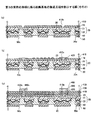
[第3の実施の形態に係る配線基板の構造]
まず、第3の実施の形態に係る配線基板の構造について説明する。図15は、第3の実施の形態に係る配線基板を例示する断面図である。図15を参照するに、第3の実施の形態に係る配線基板1Fは、配線基板1(図1参照)の絶縁層20上に絶縁層410、配線層420、絶縁層430、配線層440、絶縁層450、配線層460を順次積層した構造である。なお、図15では、配線層10、絶縁層20等が図1とは上下を反転した状態で描かれている。
[Structure of Wiring Board According to Third Embodiment]
First, the structure of the wiring board according to the third embodiment will be described. FIG. 15 is a cross-sectional view illustrating a wiring board according to the third embodiment. With reference to FIG. 15, a
絶縁層410、430、及び450の厚さは、絶縁層20の厚さよりも薄く形成されている。又、配線層420及び440を構成する配線パターンの厚さは、配線層10及び40を構成する配線パターンの厚さよりも薄く形成されている。配線層420及び440を構成する配線パターンは、配線層10及び40を構成する配線パターンよりも高密度(微細配線)である。なお、絶縁層450上に、配線層460を構成するパッドを露出するソルダーレジスト層を設けてもよい。
The thicknesses of the insulating
配線基板1Fにおいて、配線層10の他方の面と絶縁層20の他方の面(第1絶縁膜21の他方の面)は研磨されて平坦面とされている。絶縁層410は、配線層10の他方の面と絶縁層20の他方の面が形成する平坦面に形成されている。絶縁層410の材料としては、例えば、エポキシ系樹脂やフェノール系樹脂等を主成分とする感光性の絶縁性樹脂(熱硬化性)を用いることができる。絶縁層410は、シリカ(SiO2)等のフィラーを含有しても構わない。絶縁層410の厚さは、例えば、3〜30μm程度とすることができる。
In the
配線層420は、絶縁層410の他方の側に形成されている。配線層420は、ビアホール410x内に充填されたビア配線、及び絶縁層410の他方の面に形成された配線パターンを含んで構成されている。ビアホール410xは、絶縁層430側に開口されている開口部の径が配線層10の他方の面によって形成された開口部の底面の径よりも大きい逆円錐台状の凹部となっている。配線層420は、ビアホール410xを介して、配線層10と電気的に接続されている。配線層420の材料としては、例えば、銅(Cu)等を用いることができる。配線層420を構成する配線パターンの厚さは、例えば、1〜3μm程度とすることができる。
The
絶縁層430は、絶縁層410の他方の面に、配線層420を被覆するように形成されている。絶縁層430の材料や厚さは、例えば、絶縁層410と同様とすることができる。
The insulating
配線層440は、絶縁層430の他方の側に形成されている。配線層440は、ビアホール430x内に充填されたビア配線、及び絶縁層430の他方の面に形成された配線パターンを含んで構成されている。ビアホール430xは、絶縁層450側に開口されている開口部の径が配線層420の他方の面によって形成された開口部の底面の径よりも大きい逆円錐台状の凹部となっている。配線層440は、ビアホール430xを介して、配線層420と電気的に接続されている。配線層440の材料や配線層440を構成する配線パターンの厚さは、例えば、配線層420と同様とすることができる。
The
絶縁層450は、絶縁層430の他方の面に、配線層440を被覆するように形成されている。絶縁層450の材料や厚さは、例えば、絶縁層410と同様とすることができる。
The insulating
配線層460は、絶縁層450の他方の側に形成されている。配線層460は、ビアホール450x内に充填されたビア配線、及び絶縁層450の他方の面から突出するパッド(ポスト)を含んで構成されている。ビアホール450xは、配線基板1Fの外側に開口されている開口部の径が配線層440の他方の面によって形成された開口部の底面の径よりも大きい逆円錐台状の凹部となっている。配線層460は、ビアホール450xを介して、配線層440と電気的に接続されている。
The
配線層460の材料は、例えば、配線層420と同様とすることができる。配線層460の厚さ(絶縁層450の他方の面から突出するパッド部分も含む)は、例えば、10μm程度とすることができる。配線層460を構成するパッドの平面形状は、例えば、直径が20〜30μm程度の円形とすることができる。配線層460を構成するパッドのピッチは、例えば、40〜50μm程度とすることができる。配線層460を構成するパッドは、半導体チップ等と電気的に接続されるパッドとして機能する。なお、配線層460を構成するパッドの表面(上面のみ、又は上面及び側面)に前述の金属層を形成したり、酸化防止処理を施したりしてもよい。
The material of the
[第3の実施の形態に係る配線基板の製造方法]
次に、第3の実施の形態に係る配線基板の製造方法について説明する。図16及び図17は、第3の実施の形態に係る配線基板の製造工程を例示する図である。本実施の形態では、支持体上に複数の配線基板となる部分を作製し支持体を除去後個片化して各配線基板とする工程の例を示すが、支持体上に1個ずつ配線基板を作製し支持体を除去する工程としてもよい。
[Method for Manufacturing Wiring Board According to Third Embodiment]
Next, a method of manufacturing the wiring board according to the third embodiment will be described. 16 and 17 are views exemplifying the manufacturing process of the wiring board according to the third embodiment. In this embodiment mode, an example of a step in which a plurality of wiring board portions are formed over a support body, and the support body is removed and then divided into individual wiring boards is shown. However, one wiring board is formed on each support body. May be prepared and the support may be removed.
まず、図16(a)に示す工程では、図2(a)〜図3(b)と同様の工程を実行し、支持体300上に配線層10、絶縁層20、配線層40、及びソルダーレジスト層50を形成する。
First, in the step shown in FIG. 16A, the same steps as those in FIGS. 2A to 3B are performed, and the
次に、図16(b)に示す工程では、図3(c)に示す工程と同様にして、図16(a)に示す支持体300を除去する。ここで、支持体300と配線層10とが同じ金属(例えば、銅等)からなる場合、配線層10の他方の面がエッチングされ、配線層10の他方の面が第1絶縁膜21の他方の面よりも窪んだ状態になる。
Next, in the step shown in FIG. 16B, the
次に、図16(c)に示す工程では、図16(b)に示す構造体の絶縁層20の他方の面(第1絶縁膜21の他方の面)をCMP法(chemical mechanical polishing法)等を用いて研磨する。この際、配線層10の他方の面の一部を同時に研磨してもよい。これにより、配線層10の他方の面と絶縁層20の他方の面とは平坦面(面一)となる。なお、絶縁層20の第1絶縁膜21は絶縁性樹脂のみから構成されており、ガラスクロス等の補強部材を含有していないため、ガラスクロス等の補強部材が表面から突出するおそれがなく平坦化することが容易である。
Next, in the step shown in FIG. 16C, the other surface of the insulating
次に、図17(a)に示す工程では、配線層10の他方の面と絶縁層20の他方の面が形成する平坦面に絶縁層410を形成する。そして、絶縁層410に、絶縁層410を貫通し配線層10の他方の面を露出するビアホール410xを形成する。絶縁層410の材料としては、例えば、エポキシ系樹脂やフェノール系樹脂等を主成分とする感光性の絶縁性樹脂(熱硬化性)を用いることができる。
Next, in the step shown in FIG. 17A, the insulating
具体的には、例えば、配線層10の他方の面と絶縁層20の他方の面が形成する平坦面に、液状又はペースト状の絶縁性樹脂をスピンコート法等により塗布し、加熱して硬化させ、絶縁層410を形成する。そして、絶縁層410を露光及び現像し、ビアホール410xを形成する(フォトリソグラフィ法)。このように、絶縁層410の材料として感光性の絶縁性樹脂を用いることにより、フォトリソグラフィ法によりビアホール410xを形成できるため、微細配線の形成に好適である。なお、図17(a)〜図17(c)は、図16(a)〜図16(c)に対して上下が反転して描かれている。
Specifically, for example, a liquid or paste insulating resin is applied to a flat surface formed by the other surface of the
次に、図17(b)に示す工程では、絶縁層410の他方の側に、例えば、セミアディティブ法等により配線層420を形成する。次に、図17(c)に示す工程では、図17(a)及び図17(b)に示す工程を繰り返し、絶縁層410の他方の側に絶縁層430、配線層440、絶縁層450、及び配線層460を順次積層する。
Next, in the step shown in FIG. 17B, the
図17(c)の工程の後、図17(c)に示す構造体をスライサー等により個片化することにより、図15に示す配線基板1Fが複数個完成する。必要に応じ、配線層460を構成するパッドの表面(上面のみ、又は上面及び側面)に前述の金属層を形成したり、酸化防止処理を施したりしてもよい。又、絶縁層450の他方の面に、配線層460を構成するパッドを露出するソルダーレジスト層を設けてもよい。
After the step of FIG. 17C, the structure shown in FIG. 17C is separated into individual pieces by a slicer or the like to complete a plurality of
このように、第3の実施の形態に係る配線基板1Fでは、配線層10の他方の面と絶縁層20の他方の面(第1絶縁膜21の他方の面)は研磨されて平坦面とされている。そのため、その上に形成される絶縁層410、430、及び450の他方の面も平坦面となる。その結果、絶縁層410、430、及び450の各平坦面に微細な配線層420、440、及び460を容易に形成することができる。
As described above, in the
〈配線基板の応用例3〉
配線基板の応用例3では、第3の実施の形態に係る配線基板に半導体チップが搭載(フリップチップ実装)された半導体パッケージの例を示す。なお、配線基板の応用例3において、既に説明した実施の形態と同一構成部についての説明は省略する場合がある。
<Application example 3 of wiring board>
Application Example 3 of wiring board shows an example of a semiconductor package in which a semiconductor chip is mounted (flip-chip mounted) on the wiring board according to the third embodiment. In application example 3 of the wiring board, description of the same components as those in the above-described embodiments may be omitted.
図18は、応用例3に係る半導体パッケージを例示する断面図である。図18を参照するに、半導体パッケージ5Cは、図15に示す配線基板1Fと、半導体チップ100と、はんだバンプ140と、アンダーフィル樹脂120と、バンプ130とを有する。半導体パッケージ5Cにおいて、配線基板1Fの絶縁層450側が半導体チップ100が搭載されるチップ搭載面となり、配線基板1Fのソルダーレジスト層50側が外部接続端子が形成される外部接続端子面となる。
FIG. 18 is a cross-sectional view illustrating a semiconductor package according to Application Example 3. Referring to FIG. 18, the semiconductor package 5C has the
はんだバンプ140は、半導体チップ100の電極パッド(図示せず)と、配線基板1Fの配線層460を構成するパッドとを電気的に接続している。なお、半導体チップ100は銅ピラーを有していてもよい。はんだバンプ140の材料としては、例えばPbを含む合金、SnとCuの合金、SnとAgの合金、SnとAgとCuの合金等を用いることができる。
The solder bumps 140 electrically connect the electrode pads (not shown) of the
アンダーフィル樹脂120は、半導体チップ100と配線基板1F(絶縁層450)との間に充填されている。バンプ130は、ソルダーレジスト層50の開口部50xの底部に露出する配線層40の表面に形成された外部接続端子である。
The
このように、第3の実施の形態に係る配線基板1Fに半導体チップ100を搭載することにより、半導体パッケージ5Cを実現できる。
In this way, by mounting the
〈第4の実施の形態〉
第4の実施の形態では、配線層及び絶縁層が1層の配線基板の例を示す。なお、第4の実施の形態において、既に説明した実施の形態と同一構成部についての説明は省略する場合がある。
<Fourth Embodiment>
The fourth embodiment shows an example of a wiring board having one wiring layer and one insulating layer. In the fourth embodiment, description of the same components as those in the above-described embodiments may be omitted.
[第4の実施の形態に係る配線基板の構造]
まず、第4の実施の形態に係る配線基板の構造について説明する。図19は、第4の実施の形態に係る配線基板を例示する断面図であり、図19(a)は全体図、図19(b)は図19(a)のA部の部分拡大図である。図19を参照するに、第4の実施の形態に係る配線基板1Gは、配線層40並びにソルダーレジスト層50及び60を有していない点が、配線基板1(図1参照)と相違する。
[Structure of Wiring Board According to Fourth Embodiment]
First, the structure of the wiring board according to the fourth embodiment will be described. 19A and 19B are cross-sectional views illustrating the wiring board according to the fourth embodiment. FIG. 19A is an overall view, and FIG. 19B is a partially enlarged view of part A of FIG. 19A. is there. Referring to FIG. 19,
配線基板1Gは、1層の配線層10と、1層の絶縁層20とにより構成されている。配線層10は、配線基板1と同様に、半導体チップとの接続端子となる複数のパッド10aと、パッド10aと接続された配線パターン10bとを含んでいる(図1(b)参照)。
The
絶縁層20には、配線基板1と同様に、配線層10の上面を露出する開口部20xが形成されている。開口部20xは、例えば、配線層10側の径より開口側の径が大きい逆円錐台形状に形成される。但し、配線基板1とは異なり、開口部20xの第1絶縁膜21に形成された部分に、開口部20xの内壁を第1絶縁膜21側に後退させる環状の凹部20yが形成されている。凹部20yの幅W1は、例えば、1〜5μm程度とすることができる。
Like the wiring board 1, the insulating
開口部20x内に露出する配線層10は外部接続用のパッドとなる。外部接続用のパッドは、例えば、他の配線基板や半導体パッケージ、半導体チップ等と電気的に接続される。必要に応じ、開口部20x内に露出する配線層10の上面に、はんだバンプ等の外部接続端子を設けてもよい。
The
開口部20x内に露出する配線層10の上面に、はんだバンプを設けた場合、はんだバンプが凹部20y内にも入り込むため、はんだバンプの脱落を防止できる(後述の図28(b)参照)。又、凹部20yを形成したことにより、開口部20x内に露出する配線層10の上面の面積が増加するため、配線層10の上面とはんだバンプとの接触面積が拡大し、両者間の接続信頼性を向上できる。
When solder bumps are provided on the upper surface of the
なお、配線基板1と同様に、必要に応じ、開口部20x内に露出する配線層10の上面、配線層10のパッド10aの下面に金属層の形成やOSP処理を行ってもよい。
Similar to the wiring board 1, if necessary, a metal layer may be formed on the upper surface of the
[第4の実施の形態に係る配線基板の製造方法]
次に、第4の実施の形態に係る配線基板の製造方法について説明する。図20〜図22は、第4の実施の形態に係る配線基板の製造工程を例示する図である。本実施の形態では、支持体上に複数の配線基板となる部分を作製し支持体を除去後個片化して各配線基板とする工程の例を示すが、支持体上に1個ずつ配線基板を作製し支持体を除去する工程としてもよい。
[Method of Manufacturing Wiring Board According to Fourth Embodiment]
Next, a method of manufacturing the wiring board according to the fourth embodiment will be described. 20 to 22 are views exemplifying the manufacturing steps of the wiring board according to the fourth embodiment. In this embodiment mode, an example of a step in which a plurality of wiring board portions are formed over a support body, and the support body is removed and then divided into individual wiring boards is shown. However, one wiring board is formed on each support body. May be prepared and the support may be removed.
まず、図20(a)に示す工程では、上面が平坦面である支持体900を準備する。支持体900としては、例えば、プリプレグ910上にキャリア付き金属箔920が積層されたものを用いることができる。支持体900の厚さは、例えば18〜100μm程度とすることができる。
First, in the step shown in FIG. 20A, a
プリプレグ910は、例えば、ガラス繊維やアラミド繊維等の織布や不織布(図示せず)にエポキシ系樹脂等の絶縁樹脂を含侵させたものである。キャリア付き金属箔920は、銅からなる厚さ10〜50μm程度の厚箔(キャリア箔)922上に、剥離層(図示せず)を介して、銅からなる厚さ1.5〜5μm程度の薄箔921が剥離可能な状態で貼着されたものである。厚箔922は、薄箔921の取り扱いを容易にするための支持材として設けられている。厚箔922の下面は、プリプレグ910の上面に接着されている。
The
次に、図20(b)に示す工程では、支持体900を構成する薄箔921の上面に、例えば、キャリア付き金属箔920をめっき給電層に利用する電解めっき法等により、バリア層930を形成する。バリア層930は、後工程で薄箔921をエッチングで除去する際のエッチングストップ層となるものである。バリア層930の材料としては、銅からなる薄箔921のエッチング液で除去されない金属、例えば、ニッケル(Ni)等を用いることができる。バリア層930の厚さは、例えば、数μm程度とすることができる。
Next, in the step shown in FIG. 20B, a
次に、図20(c)及び図20(d)に示す工程では、バリア層930の上面に配線層10を選択的に形成する。まず、図20(c)に示す工程では、バリア層930の上面に、配線層10を形成する部分に開口部940xを備えたレジスト層940を形成する。具体的には、例えば、バリア層930の上面に、レジスト層940として感光性樹脂からなるドライフィルムレジストをラミネートする。そして、ドライフィルムレジストを露光及び現像によりパターニングし、配線層10を形成する部分にバリア層930の上面を露出する開口部940xを形成する。
Next, in the process shown in FIGS. 20C and 20D, the
次に、キャリア付き金属箔920及びバリア層930をめっき給電層に利用する電解めっき法により、レジスト層940の開口部940x内に露出するバリア層930の上面に配線層10を形成する。配線層10は、一方の面がバリア層930の上面に接し、他方の面が開口部940x内に露出する。配線層10の材料や厚さは、前述の通りである。
Next, the
次に、図20(d)に示す工程では、図20(c)に示すレジスト層940を剥離する。レジスト層940は、例えば、水酸化ナトリウム等を含有する剥離液を用いて剥離できる。これにより、バリア層930の上面に、配線層10が選択的に形成される。
Next, in the step shown in FIG. 20D, the resist
次に、図21(a)に示す工程では、図2(b)に示す工程と同様にして、バリア層930の上面に配線層10を被覆するBステージ状態(半硬化状態)の第1絶縁膜21を形成する。第1絶縁膜21は、絶縁性樹脂のみから構成されている。この工程では、第1絶縁膜21の硬化は行わない。
Next, in the step shown in FIG. 21A, similar to the step shown in FIG. 2B, the first insulation in the B stage state (semi-cured state) for covering the
次に、図21(b)に示す工程では、図2(c)に示す工程と同様にして、第1絶縁膜21の上面に、Bステージ状態(半硬化状態)の第2絶縁膜22を積層する。第2絶縁膜22は補強部材30に絶縁性樹脂を含浸させた構造の所謂プリプレグである。補強部材30の材料は、前述の通りである。第1絶縁膜21の上面に第2絶縁膜22を積層後、第1絶縁膜21及び第2絶縁膜22を所定温度に加熱して硬化させ、絶縁層20を作製する。必要に応じて、加圧しながら加熱してもよい。
Next, in the step shown in FIG. 21B, similar to the step shown in FIG. 2C, the second insulating
次に、図21(c)に示す工程では、図2(d)に示す工程と同様にして、絶縁層20に、レーザ加工法により絶縁層20(第2絶縁膜22及び第1絶縁膜21)を貫通し配線層10の上面を露出させる開口部20xを形成する。開口部20xは、例えば、配線層10側の径より開口側の径が大きい逆円錐台形状に形成される。
Next, in the step shown in FIG. 21C, similar to the step shown in FIG. 2D, the insulating layer 20 (the second insulating
次に、図21(d)に示す工程では、デスミア処理を行い、開口部20xの底部に露出する配線層10の上面に付着した絶縁層20の樹脂残渣を除去する。補強部材を有していない第1絶縁膜21は、補強部材30を有している第2絶縁膜22よりもエッチングされやすい。そのため、デスミア処理の条件を調整することで、開口部20xの第1絶縁膜21に形成された部分に、開口部20xの内壁を第1絶縁膜21側に後退させる環状の凹部20yを形成することができる。つまり、開口部20xの内壁面に段差を形成することができる。ここで、図21(d)は、1つの開口部20xの近傍の拡大断面図である。
Next, in the step shown in FIG. 21D, a desmear process is performed to remove the resin residue of the insulating
なお、デスミア処理は必要に応じて行えばよい。デスミア処理を行わない場合であって、凹部20yを形成したい場合には、図21(c)に示す工程で、レーザの照射条件を調整することで、レーザ加工のみにより凹部20yを形成できる。又、レーザ加工により凹部20yを形成し、その後デスミア処理を行って、凹部20yを拡幅することも可能である。又、第1絶縁膜21を構成する樹脂として、第2絶縁膜22を構成する樹脂よりもエッチングされやすい樹脂を選択し、凹部20yを形成し易くすることも可能である。
Note that the desmear process may be performed as needed. In the case where the desmear process is not performed and the
もちろん、レーザの照射条件を調整すること、及びデスミア処理の条件を調整することで、第1〜第3の実施の形態で示したように、開口部20xの内壁に凹部20yを形成しないようにすることも可能である。
Of course, by adjusting the laser irradiation condition and the desmearing condition, as shown in the first to third embodiments, the
次に、図22(a)に示す工程では、図21(d)に示す構造体から支持体900の一部を除去する。具体的には、支持体900に機械的な力を加え、キャリア付き金属箔920の薄箔921と厚箔922との界面を剥離する。前述のように、キャリア付き金属箔920は、薄箔921上に剥離層(図示せず)を介して厚箔922が貼着された構造を有するため、厚箔922は、剥離層(図示せず)とともに薄箔921から容易に剥離する。
Next, in the step shown in FIG. 22A, a part of the
これにより、薄箔921のみがバリア層930側に残り、支持体900を構成する他の部材(プリプレグ910及び厚箔922)が除去される。但し、剥離層とともに薄箔921から厚箔922が剥離する場合の他に、剥離層内で凝集破壊が起こり、薄箔921から厚箔922が剥離する場合もある。又、剥離層から厚箔922が剥離することで、薄箔921から厚箔922を剥離する場合もある。
As a result, only the
次に、図22(b)に示す工程では、エッチングにより銅からなる薄箔921(図22(a)参照)を除去する。銅からなる薄箔921は、例えば、過酸化水素/硫酸系水溶液や、過硫酸ナトリウム水溶液、過硫酸アンモニウム水溶液等を用いたウェットエッチングにより除去できる。なお、バリア層930がニッケル(Ni)からなる場合には、銅の上記エッチング液では除去されず、エッチングストップ層として機能するため、配線層10はエッチングされない。
Next, in the step shown in FIG. 22B, the
次に、図22(c)に示す工程では、バリア層930(図22(b)参照)を除去する。バリア層930がニッケル(Ni)からなる場合には、銅を除去せずにニッケル(Ni)を除去するエッチング液を選択することで、配線層10はエッチングせずにバリア層930のみをエッチングすることができる。これにより、絶縁層20の一方の面に配線層10の一方の面が露出する。配線層10の一方の面は、例えば、絶縁層20の一方の面と面一とすることができる。
Next, in the step shown in FIG. 22C, the barrier layer 930 (see FIG. 22B) is removed. When the
なお、必要に応じ、開口部20x内に露出する配線層10の上面、及び配線層10のパッド10aの下面に、例えば無電解めっき法等により金属層を形成してもよい。金属層の例としては、前述の通りである。又、金属層の形成に代えて、OSP処理等の酸化防止処理を施してもよい。
If necessary, a metal layer may be formed on the upper surface of the
図22(c)に示す工程の後、図22(c)に示す構造体をスライサー等により切断位置Cで切断して個片化することにより、複数の配線基板1G(図19参照)が完成する。必要に応じ、配線層10の下面や、開口部20x内に露出する配線層10の上面に、はんだバンプ等の外部接続端子を設けてもよい。
After the step shown in FIG. 22C, the plurality of
又、必要に応じ、図1に示す配線基板1と同様に、配線基板1Gのチップ搭載面側に開口部60xを備えたソルダーレジスト層60を形成してもよい。ソルダーレジスト層60は、図22(c)に示す構造体をスライサー等により切断位置Cで切断する前に形成してもよいし、後に形成してもよい。
Further, if necessary, similar to the wiring board 1 shown in FIG. 1, a solder resist
このように、配線基板1Gは1層の配線層及び絶縁層から構成されているため、薄型化が可能となる。薄型化すると配線基板に反りが発生するおそれがあるが、配線基板1Gでは、絶縁層20を第1絶縁膜21上に、補強部材30を備えた第2絶縁膜22を積層した構造としているため、反りの発生を抑制できる。具体的には、前述のように、第1絶縁膜21と第2絶縁膜22の何れについても、絶縁性樹脂の種類や厚さ、フィラーの種類や含有量等を調整し、CTE(熱膨張係数)を15ppm/℃以下にすることにより、配線基板1Gの反りを抑制可能となる。
As described above, the
又、配線基板1Gにおいて、開口部20x内に露出する配線層10の上面に、はんだバンプを設けた場合、はんだバンプが凹部20y内にも入り込むため、はんだバンプの脱落を防止できる。又、凹部20yを形成したことにより、開口部20x内に露出する配線層10の上面の面積が増加するため、配線層10の上面とはんだバンプとの接触面積が拡大し、両者間の接続信頼性を向上できる。
Further, in the
〈第4の実施の形態の変形例1〉
第4の実施の形態の変形例1では、配線基板1Gの製造方法の他の例を示す。なお、第4の実施の形態の変形例1において、既に説明した実施の形態と同一構成部についての説明は省略する場合がある。
<Modification 1 of Fourth Embodiment>
In Modification 1 of the fourth embodiment, another example of the method of manufacturing the
図23は、第4の実施の形態の変形例1に係る配線基板の製造工程を例示する図である。第4の実施の形態の変形例1では、プリプレグ910上にキャリア付き金属箔920Aが積層された支持体900Aを用いる。キャリア付き金属箔920Aは、銅からなる厚さ10〜50μm程度の厚箔(キャリア箔)922上に、剥離層(図示せず)を介して、ニッケルからなる厚さ1.5〜5μm程度の薄箔921Aが剥離可能な状態で貼着されたものである。なお、薄箔921Aがエッチングストップ層となるため、支持体900Aにバリア層930を形成しない。
FIG. 23 is a diagram illustrating a manufacturing process of the wiring board according to the modified example 1 of the fourth embodiment. In the first modification of the fourth embodiment, a
まず、図23(a)に示す工程では、図20(a)に示す工程と同様にして支持体900Aを作製する。そして、図20(c)〜図21(d)と同様の工程を実行し、支持体900A上に、直接、配線層10及び絶縁層20を積層し、絶縁層20に開口部20x及び凹部20yを形成する。
First, in the step shown in FIG. 23A, the
次に、図23(b)に示す工程では、図22(a)に示す工程と同様にして、図23(a)に示す構造体から支持体900Aを構成するプリプレグ910及び厚箔922を剥離する。これにより、薄箔921Aのみが絶縁層20側に残り、支持体900Aを構成する他の部材(プリプレグ910及び厚箔922)が除去される。
Next, in the step shown in FIG. 23B, similar to the step shown in FIG. 22A, the
次に、図23(c)に示す工程では、エッチングによりニッケルからなる薄箔921A(図23(b)参照)を除去する。銅を除去せずにニッケル(Ni)を除去するエッチング液を選択することで、配線層10はエッチングせずに薄箔921Aのみをエッチングすることができる。これにより、絶縁層20の一方の面に配線層10の一方の面が露出する。配線層10の一方の面は、例えば、絶縁層20の一方の面と面一とすることができる。
Next, in the step shown in FIG. 23C, the
図23(c)に示す工程の後、図23(c)に示す構造体をスライサー等により切断位置Cで切断して個片化することにより、複数の配線基板1G(図19参照)が完成する。
After the step shown in FIG. 23(c), the plurality of
必要に応じ、開口部20x内に露出する配線層10の上面、及び配線層10のパッド10aの下面に、例えば無電解めっき法等により金属層を形成してもよい。金属層の例としては、前述の通りである。又、金属層の形成に代えて、OSP処理等の酸化防止処理を施してもよい。又、必要に応じ、開口部20x内に露出する配線層10の上面や配線層10のパッド10aの下面に、はんだバンプ等の外部接続端子を設けてもよい。又、必要に応じ、図1に示す配線基板1と同様に、配線基板1Gのチップ搭載面側(配線層10のパッド10aの下面側)に開口部60xを備えたソルダーレジスト層60を形成してもよい。
If necessary, a metal layer may be formed on the upper surface of the
〈第4の実施の形態の変形例2〉
第4の実施の形態の変形例2では、配線層10の一方の面と絶縁層20の一方の面との位置関係が第4の実施の形態とは異なる例を示す。なお、第4の実施の形態の変形例2において、既に説明した実施の形態と同一構成部についての説明は省略する場合がある。
<Modification 2 of the fourth embodiment>
Modification 2 of the fourth embodiment shows an example in which the positional relationship between one surface of the
図24は、第4の実施の形態の変形例2に係る配線基板を例示する断面図であり、図19に対応する断面を示している。 24 is a cross-sectional view illustrating a wiring board according to Modification 2 of the fourth embodiment, and shows a cross section corresponding to FIG.
図24を参照するに、配線基板1Hは、絶縁層20の一方の面に厚さ方向に窪む凹部20zが形成され、配線層10の一方の面が凹部20z内において絶縁層20の一方の面よりも窪んだ位置に露出している点が、配線基板1G(図19参照)と相違する。配線基板1Hは、例えば、以下に示す工程により製造できる。
Referring to FIG. 24, in wiring board 1H, recessed
図25は、第4の実施の形態の変形例2に係る配線基板の製造工程を例示する図である。第4の実施の形態の変形例2では、支持体900上にバリア層930を形成しない。
FIG. 25 is a diagram illustrating a manufacturing process of the wiring board according to the second modification of the fourth embodiment. In Modification 2 of the fourth embodiment, the
まず、図25(a)に示す工程では、図20(a)に示す工程の後、図20(c)〜図21(d)と同様の工程を実行し、支持体900上に、直接、配線層10及び絶縁層20を積層し、絶縁層20に開口部20x及び凹部20yを形成する。なお、図20(b)に示す工程は実行しない(バリア層930を形成しない)。
First, in the step shown in FIG. 25A, after the step shown in FIG. 20A, the same steps as those shown in FIGS. 20C to 21D are performed to directly and directly on the
次に、図25(b)に示す工程では、図22(a)に示す工程と同様にして、図25(a)に示す構造体から支持体900を構成するプリプレグ910及び厚箔922を剥離する。これにより、薄箔921のみが絶縁層20側に残り、支持体900を構成する他の部材(プリプレグ910及び厚箔922)が除去される。
Next, in the step shown in FIG. 25B, the
次に、図25(c)に示す工程では、エッチングにより銅からなる薄箔921(図25(b)参照)を除去する。本実施の形態では、エッチングストップ層となるバリア層930が存在しないため、銅からなる配線層10の一方の面側もエッチングされ、絶縁層20の一方の面に凹部20zが形成される。そして、配線層10の一方の面が凹部20z内において絶縁層20の一方の面よりも窪んだ位置に露出する。
Next, in the step shown in FIG. 25C, the
図25(c)に示す工程の後、図25(c)に示す構造体をスライサー等により切断位置Cで切断して個片化することにより、複数の配線基板1H(図24参照)が完成する。 After the step shown in FIG. 25C, the plurality of wiring boards 1H (see FIG. 24) are completed by cutting the structure shown in FIG. 25C at a cutting position C using a slicer or the like to divide the structure into individual pieces. To do.
必要に応じ、開口部20x内に露出する配線層10の上面、及び凹部20z内に露出する配線層10のパッド10aの下面に、例えば無電解めっき法等により金属層を形成してもよい。金属層の例としては、前述の通りである。又、金属層の形成に代えて、OSP処理等の酸化防止処理を施してもよい。又、必要に応じ、開口部20x内に露出する配線層10の上面や凹部20z内に露出する配線層10のパッド10aの下面に、はんだバンプ等の外部接続端子を設けてもよい。又、必要に応じ、図1に示す配線基板1と同様に、配線基板1Hのチップ搭載面側(配線層10のパッド10aの下面側)に開口部60xを備えたソルダーレジスト層60を形成してもよい。
If necessary, a metal layer may be formed on the upper surface of the
〈第4の実施の形態の変形例3〉
第4の実施の形態の変形例3では、絶縁層20の他方の面に支持体(キャリア)を設けた例を示す。なお、第4の実施の形態の変形例3において、既に説明した実施の形態と同一構成部についての説明は省略する場合がある。
<Modification 3 of the fourth embodiment>
Modification 3 of the fourth embodiment shows an example in which a support (carrier) is provided on the other surface of the insulating
図26は、第4の実施の形態の変形例3に係る配線基板を例示する断面図であり、図19に対応する断面を示している。 FIG. 26 is a cross-sectional view illustrating a wiring board according to Modification 3 of the fourth embodiment, and shows a cross section corresponding to FIG.
図26を参照するに、配線基板1Iは、絶縁層20の他方の面に粘着層91を介して支持体95が設けられている点が、配線基板1G(図19参照)と相違する。配線基板1Iは、例えば、以下に示す工程により製造できる。
Referring to FIG. 26, wiring board 1I is different from wiring
図27は、第4の実施の形態の変形例3に係る配線基板の製造工程を例示する図である。 FIG. 27 is a diagram illustrating a manufacturing process of the wiring board according to the modification 3 of the fourth embodiment.
まず、図27(a)に示す工程では、図20(a)〜図21(d)と同様の工程を実行して図21(d)の構造体を作製する。そして、図21(d)の構造体の絶縁層20の他方の面に粘着層91を介して支持体95を設ける。粘着層91としては、例えば、アクリル系、シリコーン系、エポキシ系等の樹脂を用いることができる。支持体95としては、例えば、金属箔(例えば、銅箔)、樹脂フィルム(例えば、ポリイミドフィルム)、樹脂基板(例えば、ガラスエポキシ基板)等を用いることができる。
First, in the step shown in FIG. 27A, steps similar to those in FIGS. 20A to 21D are performed to manufacture the structure shown in FIG. Then, the
なお、後述のように、粘着層91及び支持体95を備えた配線基板1Iに半導体チップを実装する場合があるため、粘着層91及び支持体95は、リフロー等の実装工程における加熱に耐える耐熱性を有している必要がある。
As will be described later, since the semiconductor chip may be mounted on the wiring board 1I including the
次に、図27(b)に示す工程では、図22(a)に示す工程と同様にして、図27(a)に示す構造体から支持体900を構成するプリプレグ910及び厚箔922を剥離する。これにより、薄箔921のみがバリア層930側に残り、支持体900を構成する他の部材(プリプレグ910及び厚箔922)が除去される。
Next, in the step shown in FIG. 27B, similar to the step shown in FIG. 22A, the
次に、図27(c)に示す工程では、図22(b)に示す工程と同様にして、エッチングにより銅からなる薄箔921(図27(b)参照)を除去する。次に、図27(d)に示す工程では、図22(c)に示す工程と同様にして、バリア層930(図27(c)参照)を除去する。これにより、絶縁層20の一方の面に配線層10の一方の面が露出する。配線層10の一方の面は、例えば、絶縁層20の一方の面と面一とすることができる。
Next, in the step shown in FIG. 27C, the
図27(d)に示す工程の後、図27(d)に示す構造体をスライサー等により切断位置Cで切断して個片化することにより、複数の配線基板1I(図26参照)が完成する。 After the step shown in FIG. 27(d), the wiring board 1I (see FIG. 26) is completed by cutting the structure shown in FIG. 27(d) at a cutting position C by a slicer or the like to divide it into individual pieces. To do.
必要に応じ、図21(d)の構造体に支持体95を設けて図27(a)の構造体とする前に、図21(d)の構造体の開口部20x内に露出する配線層10の上面に、例えば無電解めっき法等により金属層を形成してもよい。金属層の例としては、前述の通りである。又、金属層の形成に代えて、OSP処理等の酸化防止処理を施してもよい。
If necessary, before providing the
又、必要に応じ、図27(d)に示す工程よりも後に、配線層10のパッド10aの下面に、例えば無電解めっき法等により金属層を形成してもよい。金属層の例としては、前述の通りである。又、金属層の形成に代えて、OSP処理等の酸化防止処理を施してもよい。
If necessary, after the step shown in FIG. 27D, a metal layer may be formed on the lower surface of the
又、必要に応じ、図27(d)に示す工程よりも後に、図1に示す配線基板1と同様に、配線基板1Iのチップ搭載面側(配線層10のパッド10aの下面側)に開口部60xを備えたソルダーレジスト層60を形成してもよい。
Further, if necessary, after the step shown in FIG. 27D, similar to the wiring board 1 shown in FIG. 1, an opening is made on the chip mounting surface side of the wiring board 1I (the lower surface side of the
又、図27(c)に示す構造体、すなわち、バリア層930が設けられた状態の支持体95付き配線基板を製品出荷形態としてもよい。又、図27(c)に示す構造体又は図27(d)に示す構造体は、個片化前の状態を製品出荷形態としてもよいし、個片化後の状態を製品出荷形態としてもよい。
The structure shown in FIG. 27C, that is, the wiring board with the
配線基板1Iは、絶縁層20の他方の面に支持体95が設けられているため、配線基板1I全体の剛性を高めることができる。そのため、例えば、後述の図29に示すように、配線基板1Iの出荷後に半導体チップを実装する際の取り扱いが容易となる。
Since the wiring board 1I is provided with the
なお、図24に示す配線基板1Hに支持体95を設けてもよい。又、配線基板1Hの製造途中の構造体を用い、図27の工程を行ってもよい。
The
〈配線基板の応用例4〉
配線基板の応用例4では、第4の実施の形態に係る配線基板に半導体チップが搭載(フリップチップ実装)された半導体パッケージの例を示す。なお、配線基板の応用例4において、既に説明した実施の形態と同一構成部についての説明は省略する場合がある。
<Application example 4 of wiring board>
The wiring board application example 4 shows an example of a semiconductor package in which a semiconductor chip is mounted (flip-chip mounted) on the wiring board according to the fourth embodiment. In the application example 4 of the wiring board, description of the same components as those in the above-described embodiments may be omitted.
図28は、応用例4に係る半導体パッケージを例示する断面図であり、図28(a)は全体図、図28(b)は図28(a)のB部の部分拡大図である。図28を参照するに、半導体パッケージ5Dは、図19に示す配線基板1Gと、半導体チップ100と、バンプ110と、アンダーフィル樹脂120と、バンプ130と、封止樹脂150とを有する。
28A and 28B are cross-sectional views illustrating a semiconductor package according to Application Example 4, FIG. 28A is an overall view, and FIG. 28B is a partially enlarged view of a portion B of FIG. 28A. Referring to FIG. 28, the semiconductor package 5D has the
封止樹脂150は、半導体チップ100とアンダーフィル樹脂120を被覆するように配線基板1G上に形成されている。但し、封止樹脂150の上面に半導体チップ100の上面(背面)を露出させてもよい。封止樹脂150としては、例えば、フィラーを含有した熱硬化性のエポキシ系樹脂等の絶縁樹脂(所謂モールド樹脂)を用いることができる。
The sealing
但し、アンダーフィル樹脂120は、必要に応じて設ければよい。又、封止樹脂150は設けずに、アンダーフィル樹脂120のみを設けてもよい。
However, the
バンプ130は、開口部20xに露出する配線層10の一方の面に形成された外部接続端子である。前述のように、バンプ130は、例えば、はんだバンプである。配線基板1Gでは、開口部20xの第1絶縁膜21に形成された部分に、開口部20xの内壁を第1絶縁膜21側に後退させる環状の凹部20yが形成されているため、バンプ130の一部が凹部20y内にも入り込む。そのため、はんだバンプ130の脱落を防止できる。又、凹部20yを形成したことにより、開口部20x内に露出する配線層10の一方の面の面積が増加するため、配線層10の一方の面とバンプ130との接触面積が拡大し、両者間の接続信頼性を向上できる。
The
半導体パッケージ5Dを作製するには、例えば、配線基板1Gのチップ搭載面に、ペースト状のバンプ110を介して半導体チップ100をフェースダウンで搭載する。そして、リフロー等により、バンプ110を溶融後凝固させ、半導体チップ100の電極パッド(図示せず)と、配線基板1Gのパッド10aとを電気的に接続する。
To manufacture the semiconductor package 5D, for example, the
その後、半導体チップ100と配線基板1G(絶縁層20)との間に必要に応じてアンダーフィル樹脂120を充填後、半導体チップ100とアンダーフィル樹脂120を被覆するように配線基板1G上に封止樹脂150を形成する。封止樹脂150は、例えば、封止金型を用いたトランスファーモールド法等により形成することができる。
After that, after filling the
なお、半導体パッケージ5Dにおいて、配線基板1Gに代えて配線基板1H又は1Iを用いてもよい。配線基板1Iを用いる場合には、図29(a)に示すように、図27(d)の工程を経た配線基板1Iを個片化せずに、配線基板1Iとなる各領域のチップ搭載面に、ペースト状のバンプ110を介して半導体チップ100をフェースダウンで搭載する。
In the semiconductor package 5D, the wiring board 1H or 1I may be used instead of the
そして、リフロー等により、バンプ110を溶融後凝固させ、半導体チップ100の電極パッド(図示せず)と、配線基板1Iとなる各領域のパッド10aとを電気的に接続する。そして、半導体チップ100と絶縁層20との間に必要に応じてアンダーフィル樹脂120を充填する。更に、半導体チップ100とアンダーフィル樹脂120を被覆するように配線基板1Iとなる各領域上にトランスファーモールド法等により封止樹脂150を形成する。なお、図27と図29とは、配線基板の上下が反転した状態で描かれている。
Then, the
次に、図29(b)に示すように、図29(a)に示す支持体95に機械的な力を加え、粘着層91及び支持体95を絶縁層20から剥離する。そして、図29(c)に示すように、開口部20x内に露出する配線層10上に、はんだバンプ等のバンプ130を形成する。
Next, as shown in FIG. 29B, a mechanical force is applied to the
図29(c)に示す工程の後、図29(c)に示す構造体をスライサー等により切断位置Cで切断して個片化することにより、複数の半導体パッケージ5D(図28参照)が完成する。 After the step shown in FIG. 29C, the structure shown in FIG. 29C is cut at a cutting position C by a slicer or the like to be separated into a plurality of semiconductor packages 5D (see FIG. 28). To do.
このように、配線基板1G〜1Iに半導体チップ100を搭載することにより、半導体パッケージ5Dを実現できる。図29に示す製造方法では、封止樹脂150を形成後に支持体95を除去するため、配線基板の剛性が低い場合でも配線基板の変形を防止できる。
In this way, the semiconductor package 5D can be realized by mounting the
以上、好ましい実施の形態等について詳説したが、上述した実施の形態等に制限されることはなく、特許請求の範囲に記載された範囲を逸脱することなく、上述した実施の形態等に種々の変形及び置換を加えることができる。 Although the preferred embodiments and the like have been described in detail above, the present invention is not limited to the above-described embodiments and the like, and various embodiments and the like described above can be performed without departing from the scope described in the claims. Modifications and substitutions can be added.
例えば、上記の実施の形態等では、第1絶縁膜21の下面と配線層10の下面(露出面)とが面一である例や、配線層10の下面が第1絶縁膜21の下面よりも窪んだ位置にある例を示した。しかし、配線層10の下面は第1絶縁膜21の下面よりも突出した位置にあってもよい。
For example, in the above-described embodiments, the lower surface of the first insulating
又、第1〜第3の実施の形態において、支持体300として、銅以外に、ニッケル、クロム、鉄等、銅からなる配線層10とは異なるエッチング液で除去可能な金属箔や金属板を用いてもよい。この場合、配線層10の下面が第1絶縁膜21の下面と面一となる。
In addition, in the first to third embodiments, as the
又、第1〜第3の実施の形態において、配線層10と同じ金属からなる支持体300の上面に、配線層10と異なる金属からなるエッチングバリア層を設けてもよい。例えば、配線層10及び支持体300が共に銅である場合、支持体300の上面全面に、電解めっき法等により、ニッケル、クロム、鉄等からなるエッチングバリア層を形成する。その後、エッチングバリア層上に配線層10、絶縁層20等を順次積層する。そして、支持体300をエッチングで除去し、次いで、エッチングバリア層を(配線層10をエッチングしないエッチング液を用いて)エッチングで除去し、配線基板が完成する。この場合も、配線層10の下面が第1絶縁膜21の下面と面一となる。
Further, in the first to third embodiments, an etching barrier layer made of a metal different from the
1、1A、1B、1C、1D、1E、1F、1G、1H、1I 配線基板
5、5A、5B、5C、5D 半導体パッケージ
10、40、80、420、440、460 配線層
10a パッド
10b 配線パターン
20、20A、70、410、430、450 絶縁層
20x、50x、60x 開口部
20y 凹部
21 第1絶縁膜
22 第2絶縁膜
23 第3絶縁膜
30 補強部材
50、60 ソルダーレジスト層
70x、410x、430x、450x ビアホール
91 粘着層
95、300、900 支持体
100、210、250 半導体チップ
110、130、220、260、280 バンプ
120 アンダーフィル樹脂
140 はんだバンプ
150、240 封止樹脂
230 はんだボール
231 銅コアボール
232 はんだ
270 チップコンデンサ
910 プリプレグ
920、920A キャリア付き金属箔
921、921A 薄箔
922 厚箔
930 バリア層
940 レジスト層
1, 1A, 1B, 1C, 1D, 1E, 1F, 1G, 1H,
Claims (14)
前記第1絶縁膜に埋め込まれ、所定面が前記第1絶縁膜の他方の面から露出する第1配線層と、を有し、
前記絶縁層は、前記第1絶縁膜及び前記第2絶縁膜を貫通し、前記第1配線層の前記所定面の反対面を露出する開口部を備え、
前記開口部の前記第1絶縁膜に形成された部分に、前記開口部の内壁を前記第1絶縁膜側に後退させる凹部が形成され、
前記開口部の前記第2絶縁膜に形成された部分は、前記凹部と連通する部分で径が最小となる逆円錐台形状であり、
前記第1絶縁膜は前記第2絶縁膜よりもエッチングされやすく、
前記第1絶縁膜は、前記第1配線層の側面と、前記所定面の反対面を被覆し、
前記第1絶縁膜は樹脂のみから構成され、
前記第2絶縁膜は補強部材に樹脂を含浸させた構成とされている配線基板。 An insulating layer in which a second insulating film is laminated on one surface of the first insulating film, and the other surface of the first insulating film is exposed to the outside;
A first wiring layer embedded in the first insulating film and having a predetermined surface exposed from the other surface of the first insulating film,
The insulating layer includes an opening that penetrates the first insulating film and the second insulating film and exposes a surface of the first wiring layer opposite to the predetermined surface.
In a portion of the opening formed in the first insulating film, a concave portion is formed to recede an inner wall of the opening toward the first insulating film,
The portion of the opening formed in the second insulating film has an inverted truncated cone shape having a minimum diameter in a portion communicating with the recess,
The first insulating film is more easily etched than the second insulating film,
The first insulating film covers a side surface of the first wiring layer and a surface opposite to the predetermined surface,
The first insulating film is composed only of resin,
The second insulating film is a wiring board in which a reinforcing member is impregnated with a resin.
前記他の絶縁層に積層され、前記第2配線層の配線パターンと接続される第3配線層と、を有する請求項5記載の配線基板。 Another insulating layer laminated on the second insulating film so as to cover the wiring pattern of the second wiring layer,
The wiring board according to claim 5 , further comprising a third wiring layer laminated on the other insulating layer and connected to a wiring pattern of the second wiring layer.
前記支持体の上面に、前記第1配線層の上面及び側面を被覆するように、樹脂のみから構成された半硬化状態の第1絶縁膜を形成する工程と、
前記第1絶縁膜の一方の面上に、補強部材に樹脂を含浸させた構成とされた半硬化状態の第2絶縁膜を積層する工程と、
前記第1絶縁膜及び前記第2絶縁膜を硬化させ、前記第1絶縁膜上に前記第2絶縁膜が積層された絶縁層を作製する工程と、
前記絶縁層の前記第1絶縁膜及び前記第2絶縁膜を貫通し、前記第1配線層の上面を露出する開口部を形成する工程と、
前記開口部の前記第1絶縁膜に形成された部分に、デスミア処理の条件を調整することで、前記開口部の内壁を前記第1絶縁膜側に後退させる凹部を形成する工程と、を有し、
前記開口部の前記第2絶縁膜に形成された部分は、前記凹部と連通する部分で径が最小となる逆円錐台形状となり、
前記第1絶縁膜は前記第2絶縁膜よりもエッチングされやすい配線基板の製造方法。 A step of forming a first wiring layer on the upper surface of the support,
Forming a semi-cured first insulating film made of only resin on the upper surface of the support so as to cover the upper surface and side surfaces of the first wiring layer;
Stacking a semi-cured second insulating film having a structure in which a reinforcing member is impregnated with a resin on one surface of the first insulating film;
Curing the first insulating film and the second insulating film to produce an insulating layer in which the second insulating film is laminated on the first insulating film;
Forming an opening that penetrates the first insulating film and the second insulating film of the insulating layer and exposes an upper surface of the first wiring layer;
Forming a recess in the portion of the opening formed in the first insulating film to adjust the conditions of the desmearing process so that the inner wall of the opening recedes toward the first insulating film. Then
A portion of the opening formed in the second insulating film has an inverted truncated cone shape having a minimum diameter in a portion communicating with the recess,
The method of manufacturing a wiring board, wherein the first insulating film is more easily etched than the second insulating film .
樹脂のみから構成された半硬化状態の第1絶縁膜、及び前記第1絶縁膜の一方の面上に積層された、補強部材に樹脂を含浸させた構成とされた半硬化状態の第2絶縁膜、を有する絶縁層を準備する工程と、
前記第1絶縁膜を前記支持体側に向けて、前記支持体の上面に前記第1配線層の上面及び側面を被覆するように前記絶縁層を貼り付け、前記絶縁層を硬化させる工程と、
前記絶縁層の前記第1絶縁膜及び前記第2絶縁膜を貫通し、前記第1配線層の上面を露出する開口部を形成する工程と、
前記開口部の前記第1絶縁膜に形成された部分に、デスミア処理の条件を調整することで、前記開口部の内壁を前記第1絶縁膜側に後退させる凹部を形成する工程と、を有し、
前記開口部の前記第2絶縁膜に形成された部分は、前記凹部と連通する部分で径が最小となる逆円錐台形状となり、
前記第1絶縁膜は前記第2絶縁膜よりもエッチングされやすい配線基板の製造方法。 A step of forming a first wiring layer on the upper surface of the support,
A semi-cured first insulating film composed only of a resin, and a semi-cured second insulating film laminated on one surface of the first insulating film and having a reinforcing member impregnated with the resin. A step of preparing an insulating layer having a film,
A step of sticking the insulating layer to the upper surface of the support so as to cover the upper surface and side surfaces of the first wiring layer with the first insulating film facing the support, and curing the insulating layer;
Forming an opening that penetrates the first insulating film and the second insulating film of the insulating layer and exposes an upper surface of the first wiring layer;
Forming a recess in the portion of the opening formed in the first insulating film to adjust the conditions of the desmearing process so that the inner wall of the opening recedes toward the first insulating film. Then
A portion of the opening formed in the second insulating film has an inverted truncated cone shape having a minimum diameter in a portion communicating with the recess,
The method of manufacturing a wiring board, wherein the first insulating film is more easily etched than the second insulating film .
Priority Applications (3)
| Application Number | Priority Date | Filing Date | Title |
|---|---|---|---|
| JP2016156803A JP6705718B2 (en) | 2016-08-09 | 2016-08-09 | Wiring board and manufacturing method thereof |
| US15/663,962 US20180047661A1 (en) | 2016-08-09 | 2017-07-31 | Wiring board |
| US16/701,416 US11152293B2 (en) | 2016-08-09 | 2019-12-03 | Wiring board having two insulating films and hole penetrating therethrough |
Applications Claiming Priority (1)
| Application Number | Priority Date | Filing Date | Title |
|---|---|---|---|
| JP2016156803A JP6705718B2 (en) | 2016-08-09 | 2016-08-09 | Wiring board and manufacturing method thereof |
Publications (3)
| Publication Number | Publication Date |
|---|---|
| JP2018026437A JP2018026437A (en) | 2018-02-15 |
| JP2018026437A5 JP2018026437A5 (en) | 2019-05-09 |
| JP6705718B2 true JP6705718B2 (en) | 2020-06-03 |
Family
ID=61160417
Family Applications (1)
| Application Number | Title | Priority Date | Filing Date |
|---|---|---|---|
| JP2016156803A Active JP6705718B2 (en) | 2016-08-09 | 2016-08-09 | Wiring board and manufacturing method thereof |
Country Status (2)
| Country | Link |
|---|---|
| US (2) | US20180047661A1 (en) |
| JP (1) | JP6705718B2 (en) |
Families Citing this family (6)
| Publication number | Priority date | Publication date | Assignee | Title |
|---|---|---|---|---|
| JP7147223B2 (en) * | 2018-03-30 | 2022-10-05 | 住友ベークライト株式会社 | Method for manufacturing coreless substrate and method for manufacturing printed wiring board |
| JP7202785B2 (en) * | 2018-04-27 | 2023-01-12 | 新光電気工業株式会社 | Wiring board and method for manufacturing wiring board |
| CN110556356A (en) * | 2018-06-01 | 2019-12-10 | 夏普株式会社 | power module |
| JP7289620B2 (en) * | 2018-09-18 | 2023-06-12 | 新光電気工業株式会社 | Wiring substrates, laminated wiring substrates, semiconductor devices |
| US10978417B2 (en) * | 2019-04-29 | 2021-04-13 | Advanced Semiconductor Engineering, Inc. | Wiring structure and method for manufacturing the same |
| JP2022030237A (en) * | 2020-08-06 | 2022-02-18 | 新光電気工業株式会社 | Manufacturing method of wiring board and insulation sheet |
Family Cites Families (17)
| Publication number | Priority date | Publication date | Assignee | Title |
|---|---|---|---|---|
| JPH11224918A (en) * | 1997-12-03 | 1999-08-17 | Mitsui High Tec Inc | Semiconductor device and manufacture thereof |
| JP4045708B2 (en) * | 1999-12-08 | 2008-02-13 | ソニー株式会社 | Semiconductor device, electronic circuit device and manufacturing method |
| JP4108643B2 (en) | 2004-05-12 | 2008-06-25 | 日本電気株式会社 | Wiring board and semiconductor package using the same |
| US8044505B2 (en) | 2005-12-01 | 2011-10-25 | Sumitomo Bakelite Company Limited | Prepreg, method for manufacturing prepreg, substrate, and semiconductor device |
| CN101321813B (en) * | 2005-12-01 | 2012-07-04 | 住友电木株式会社 | Prepreg, process for producing prepreg, substrate, and semiconductor device |
| JP2007329303A (en) * | 2006-06-08 | 2007-12-20 | Matsushita Electric Ind Co Ltd | Carrier for transfer of thin printed wiring circuit board |
| JP5117692B2 (en) | 2006-07-14 | 2013-01-16 | ルネサスエレクトロニクス株式会社 | Manufacturing method of semiconductor device |
| JP5324051B2 (en) * | 2007-03-29 | 2013-10-23 | 新光電気工業株式会社 | Wiring substrate manufacturing method, semiconductor device manufacturing method, and wiring substrate |
| TWI389279B (en) | 2009-01-23 | 2013-03-11 | Unimicron Technology Corp | Printed circuit board structure and fabrication method thereof |
| EP2448378A1 (en) * | 2010-10-26 | 2012-05-02 | ATOTECH Deutschland GmbH | Composite build-up materials for embedding of active components |
| JP2013149941A (en) * | 2011-12-22 | 2013-08-01 | Ngk Spark Plug Co Ltd | Multilayer wiring substrate and manufacturing method of the same |
| JP5990421B2 (en) * | 2012-07-20 | 2016-09-14 | 新光電気工業株式会社 | Wiring substrate, manufacturing method thereof, and semiconductor package |
| KR20160010960A (en) * | 2014-07-21 | 2016-01-29 | 삼성전기주식회사 | Printed circuit board and manufacturing method thereof |
| JP2016035969A (en) * | 2014-08-01 | 2016-03-17 | 味の素株式会社 | Circuit board and method for manufacturing the same |
| JP5795415B1 (en) * | 2014-08-29 | 2015-10-14 | 新光電気工業株式会社 | Wiring board and manufacturing method thereof |
| JP2016063130A (en) | 2014-09-19 | 2016-04-25 | イビデン株式会社 | Printed wiring board and semiconductor package |
| US9426891B2 (en) * | 2014-11-21 | 2016-08-23 | Advanced Semiconductor Engineering, Inc. | Circuit board with embedded passive component and manufacturing method thereof |
-
2016
- 2016-08-09 JP JP2016156803A patent/JP6705718B2/en active Active
-
2017
- 2017-07-31 US US15/663,962 patent/US20180047661A1/en not_active Abandoned
-
2019
- 2019-12-03 US US16/701,416 patent/US11152293B2/en active Active
Also Published As
| Publication number | Publication date |
|---|---|
| US20180047661A1 (en) | 2018-02-15 |
| US20200105651A1 (en) | 2020-04-02 |
| JP2018026437A (en) | 2018-02-15 |
| US11152293B2 (en) | 2021-10-19 |
Similar Documents
| Publication | Publication Date | Title |
|---|---|---|
| JP6705718B2 (en) | Wiring board and manufacturing method thereof | |
| JP6358887B2 (en) | Support, wiring board, method for manufacturing the same, and method for manufacturing semiconductor package | |
| JP5795415B1 (en) | Wiring board and manufacturing method thereof | |
| JP4334005B2 (en) | Wiring board manufacturing method and electronic component mounting structure manufacturing method | |
| JP6133227B2 (en) | Wiring board and manufacturing method thereof | |
| JP5410660B2 (en) | WIRING BOARD AND ITS MANUFACTURING METHOD, ELECTRONIC COMPONENT DEVICE AND ITS MANUFACTURING METHOD | |
| JP5649490B2 (en) | Wiring board and manufacturing method thereof | |
| JP6584939B2 (en) | Wiring board, semiconductor package, semiconductor device, wiring board manufacturing method, and semiconductor package manufacturing method | |
| JP6761064B2 (en) | Wiring board and its manufacturing method | |
| JP4635033B2 (en) | Wiring board manufacturing method and electronic component mounting structure manufacturing method | |
| JP2005216936A (en) | Semiconductor device and its production process | |
| JP6594264B2 (en) | Wiring board, semiconductor device, and manufacturing method thereof | |
| JP6691451B2 (en) | Wiring board, manufacturing method thereof, and electronic component device | |
| US9334576B2 (en) | Wiring substrate and method of manufacturing wiring substrate | |
| KR20150004749A (en) | Wiring substrate, method for manufacturing wiring substrate, and semiconductor package | |
| JP2019192886A (en) | Wiring board and method for manufacturing wiring board | |
| JP6341714B2 (en) | Wiring board and manufacturing method thereof | |
| US9961767B2 (en) | Circuit board and method of manufacturing circuit board | |
| JP6671256B2 (en) | Wiring board and manufacturing method thereof | |
| JP5432354B2 (en) | Temporary board for manufacturing wiring board and method for manufacturing the same | |
| JP6107021B2 (en) | Wiring board manufacturing method | |
| JP2008181920A (en) | Substrate with built-in electronic component and electronic equipment using the same, and method of manufacturing substrate with built-in electronic component | |
| JP6623056B2 (en) | Wiring board, semiconductor device | |
| JP2016152362A (en) | Wiring board and semiconductor package | |
| JP2019016683A (en) | Wiring board and manufacturing method of the same, and semiconductor package |
Legal Events
| Date | Code | Title | Description |
|---|---|---|---|
| A521 | Written amendment |
Free format text: JAPANESE INTERMEDIATE CODE: A523 Effective date: 20190319 |
|
| A621 | Written request for application examination |
Free format text: JAPANESE INTERMEDIATE CODE: A621 Effective date: 20190319 |
|
| A977 | Report on retrieval |
Free format text: JAPANESE INTERMEDIATE CODE: A971007 Effective date: 20191213 |
|
| A131 | Notification of reasons for refusal |
Free format text: JAPANESE INTERMEDIATE CODE: A131 Effective date: 20191224 |
|
| A521 | Written amendment |
Free format text: JAPANESE INTERMEDIATE CODE: A523 Effective date: 20200218 |
|
| TRDD | Decision of grant or rejection written | ||
| A01 | Written decision to grant a patent or to grant a registration (utility model) |
Free format text: JAPANESE INTERMEDIATE CODE: A01 Effective date: 20200428 |
|
| A61 | First payment of annual fees (during grant procedure) |
Free format text: JAPANESE INTERMEDIATE CODE: A61 Effective date: 20200514 |
|
| R150 | Certificate of patent or registration of utility model |
Ref document number: 6705718 Country of ref document: JP Free format text: JAPANESE INTERMEDIATE CODE: R150 |