JP6700933B2 - Image forming device - Google Patents

Image forming device Download PDF

Info

Publication number
JP6700933B2
JP6700933B2 JP2016084761A JP2016084761A JP6700933B2 JP 6700933 B2 JP6700933 B2 JP 6700933B2 JP 2016084761 A JP2016084761 A JP 2016084761A JP 2016084761 A JP2016084761 A JP 2016084761A JP 6700933 B2 JP6700933 B2 JP 6700933B2
Authority
JP
Japan
Prior art keywords
image
color
streak
toner
streaks
Prior art date
Legal status (The legal status is an assumption and is not a legal conclusion. Google has not performed a legal analysis and makes no representation as to the accuracy of the status listed.)
Active
Application number
JP2016084761A
Other languages
Japanese (ja)
Other versions
JP2017194573A5 (en
JP2017194573A (en
Inventor
弘 冨井
弘 冨井
Current Assignee (The listed assignees may be inaccurate. Google has not performed a legal analysis and makes no representation or warranty as to the accuracy of the list.)
Canon Inc
Original Assignee
Canon Inc
Priority date (The priority date is an assumption and is not a legal conclusion. Google has not performed a legal analysis and makes no representation as to the accuracy of the date listed.)
Filing date
Publication date
Application filed by Canon Inc filed Critical Canon Inc
Priority to JP2016084761A priority Critical patent/JP6700933B2/en
Priority to US15/478,450 priority patent/US10386767B2/en
Publication of JP2017194573A publication Critical patent/JP2017194573A/en
Publication of JP2017194573A5 publication Critical patent/JP2017194573A5/ja
Application granted granted Critical
Publication of JP6700933B2 publication Critical patent/JP6700933B2/en
Active legal-status Critical Current
Anticipated expiration legal-status Critical

Links

Images

Classifications

    • GPHYSICS
    • G03PHOTOGRAPHY; CINEMATOGRAPHY; ANALOGOUS TECHNIQUES USING WAVES OTHER THAN OPTICAL WAVES; ELECTROGRAPHY; HOLOGRAPHY
    • G03GELECTROGRAPHY; ELECTROPHOTOGRAPHY; MAGNETOGRAPHY
    • G03G15/00Apparatus for electrographic processes using a charge pattern
    • G03G15/50Machine control of apparatus for electrographic processes using a charge pattern, e.g. regulating differents parts of the machine, multimode copiers, microprocessor control
    • G03G15/5054Machine control of apparatus for electrographic processes using a charge pattern, e.g. regulating differents parts of the machine, multimode copiers, microprocessor control by measuring the characteristics of an intermediate image carrying member or the characteristics of an image on an intermediate image carrying member, e.g. intermediate transfer belt or drum, conveyor belt
    • G03G15/5058Machine control of apparatus for electrographic processes using a charge pattern, e.g. regulating differents parts of the machine, multimode copiers, microprocessor control by measuring the characteristics of an intermediate image carrying member or the characteristics of an image on an intermediate image carrying member, e.g. intermediate transfer belt or drum, conveyor belt using a test patch
    • GPHYSICS
    • G03PHOTOGRAPHY; CINEMATOGRAPHY; ANALOGOUS TECHNIQUES USING WAVES OTHER THAN OPTICAL WAVES; ELECTROGRAPHY; HOLOGRAPHY
    • G03GELECTROGRAPHY; ELECTROPHOTOGRAPHY; MAGNETOGRAPHY
    • G03G15/00Apparatus for electrographic processes using a charge pattern
    • G03G15/50Machine control of apparatus for electrographic processes using a charge pattern, e.g. regulating differents parts of the machine, multimode copiers, microprocessor control
    • G03G15/5062Machine control of apparatus for electrographic processes using a charge pattern, e.g. regulating differents parts of the machine, multimode copiers, microprocessor control by measuring the characteristics of an image on the copy material
    • GPHYSICS
    • G03PHOTOGRAPHY; CINEMATOGRAPHY; ANALOGOUS TECHNIQUES USING WAVES OTHER THAN OPTICAL WAVES; ELECTROGRAPHY; HOLOGRAPHY
    • G03GELECTROGRAPHY; ELECTROPHOTOGRAPHY; MAGNETOGRAPHY
    • G03G15/00Apparatus for electrographic processes using a charge pattern
    • G03G15/55Self-diagnostics; Malfunction or lifetime display
    • G03G15/553Monitoring or warning means for exhaustion or lifetime end of consumables, e.g. indication of insufficient copy sheet quantity for a job
    • GPHYSICS
    • G03PHOTOGRAPHY; CINEMATOGRAPHY; ANALOGOUS TECHNIQUES USING WAVES OTHER THAN OPTICAL WAVES; ELECTROGRAPHY; HOLOGRAPHY
    • G03GELECTROGRAPHY; ELECTROPHOTOGRAPHY; MAGNETOGRAPHY
    • G03G2215/00Apparatus for electrophotographic processes
    • G03G2215/01Apparatus for electrophotographic processes for producing multicoloured copies
    • G03G2215/0103Plural electrographic recording members
    • G03G2215/0119Linear arrangement adjacent plural transfer points
    • G03G2215/0122Linear arrangement adjacent plural transfer points primary transfer to an intermediate transfer belt
    • G03G2215/0125Linear arrangement adjacent plural transfer points primary transfer to an intermediate transfer belt the linear arrangement being horizontal or slanted
    • G03G2215/0129Linear arrangement adjacent plural transfer points primary transfer to an intermediate transfer belt the linear arrangement being horizontal or slanted horizontal medium transport path at the secondary transfer
    • GPHYSICS
    • G03PHOTOGRAPHY; CINEMATOGRAPHY; ANALOGOUS TECHNIQUES USING WAVES OTHER THAN OPTICAL WAVES; ELECTROGRAPHY; HOLOGRAPHY
    • G03GELECTROGRAPHY; ELECTROPHOTOGRAPHY; MAGNETOGRAPHY
    • G03G2215/00Apparatus for electrophotographic processes
    • G03G2215/01Apparatus for electrophotographic processes for producing multicoloured copies
    • G03G2215/0151Apparatus for electrophotographic processes for producing multicoloured copies characterised by the technical problem
    • G03G2215/0164Uniformity control of the toner density at separate colour transfers

Description

本発明は画像形成装置およびテストチャートに関する。   The present invention relates to an image forming apparatus and a test chart.

電子写真方式の画像形成装置は、帯電部、露光部および現像部など様々な交換可能な部品を有している。ユーザやサービスマンは出力画像を目視してどの交換部品を交換すべきかを判断するが、この判断は難しい。交換部品の見極めに時間がかかれば、ユーザが画像を形成できない時間(いわゆるダウンタイム)が長くなってしまう。   The electrophotographic image forming apparatus has various replaceable parts such as a charging part, an exposing part, and a developing part. A user or a service person visually checks the output image to determine which replacement part should be replaced, but this determination is difficult. If it takes time to identify replacement parts, the time during which the user cannot form an image (so-called downtime) becomes long.

特許文献1によればイエローパターン、マゼンタパターン、シアンパターンおよびブラックパターンを形成し、異常の発生したカラーパターンを形成したプロセスユニットの交換が必要と報知することが記載されている。プロセスユニットには感光ドラム、帯電部、現像部およびクリーニング部が一体化されているため、これらの部品がまとめて交換される。特許文献2によれば、露光がない状態と露光が有る状態でテスト画像を形成することで画像エラーの原因が露光部にあるのか、帯電部にあるのかを判定する画像形成装置が提案されている。   According to Patent Document 1, it is described that a yellow pattern, a magenta pattern, a cyan pattern, and a black pattern are formed, and that it is necessary to replace the process unit in which the abnormal color pattern is formed. Since the photosensitive drum, the charging unit, the developing unit, and the cleaning unit are integrated in the process unit, these parts are collectively replaced. According to Patent Document 2, an image forming apparatus is proposed which determines whether the cause of an image error is in an exposed portion or a charged portion by forming a test image in a state where there is no exposure and a state where there is exposure. There is.

特開2009―42691号公報JP, 2009-42691, A 特開2009―63810号公報JP, 2009-63810, A

特許文献1ではどの色のプロセスユニットを交換すべきかが特定されるが、帯電部と現像部とを個別に交換することができない。つまり、特許文献1では帯電部と現像部とのどちらを交換すべきかを特定することができない。特許文献2では露光部と帯電部とのどちらを交換すべきかを特定できるが、帯電部と現像部とのどちらを交換すべきかを特定することができない。そこで、本発明は、帯電手段と現像手段とのどちらを交換すべきかを特定可能なテスト画像を形成する画像形成装置を提供することを目的とする。   Although Patent Document 1 specifies which color of the process unit should be replaced, the charging unit and the developing unit cannot be replaced individually. That is, in Patent Document 1, it is not possible to specify which of the charging unit and the developing unit should be replaced. In Patent Document 2, it is possible to specify which of the exposed section and the charging section should be replaced, but it is not possible to specify which of the charging section and the developing section should be replaced. Therefore, an object of the present invention is to provide an image forming apparatus for forming a test image capable of specifying which of the charging unit and the developing unit should be replaced.

本願発明は、たとえば、
第一色のトナーにより現像されたトナー画像を担持する第一感光体と、
前記第一感光体に対して設けられた第一帯電器と、
前記第一感光体に対して光を照射して静電潜像を形成する第一露光器と、
前記第一色のトナーを用いてトナー画像を形成する第一現像器と、
中間転写体と、
前記中間転写体に前記第一色のトナーを用いて形成されたトナー画像を一次転写する第一の一次転写器と、
第二色のトナーにより現像されたトナー画像を担持する第二感光体と、
前記第二感光体に対して設けられた第二帯電器と、
前記第二感光体に対して光を照射して静電潜像を形成する第二露光器と、
前記第二色のトナーを用いてトナー画像を形成する第二現像器と、
前記中間転写体に前記第二色のトナーを用いて形成されたトナー画像を一次転写する第二の一次転写器と、
前記中間転写体に一次転写されたトナー画像をシートに二次転写する二次転写手段と、
前記シートに二次転写されたトナー画像を当該シートに定着させる定着手段と、
前記シートに形成された、交換部品を特定するためのテスト画像であって、露光が適用されて形成されるトナー画像である露光像と、第一帯電電位が適用されかつ露光が適用されずに形成されたトナー画像である第一非露光像と、前記第一帯電電位と異なる第二帯電電位が適用されかつ露光が適用されずに形成されたトナー画像である第二非露光像とを有するテスト画像を読み取る読取手段と、
前記第一色のトナーのみにより形成された前記テスト画像の読取結果と、前記第二色のトナーのみにより形成された前記テスト画像の読取結果と、前記交換部品を特定するための特定条件とを比較することで前記交換部品を特定する特定手段と、
前記特定手段により特定された前記交換部品を示すメッセージを出力する出力手段と、を有し、
前記特定手段は、
前記テスト画像の周囲に形成された白地部に前記第一色のスジが形成されている場合、前記第一感光体の清掃手段を前記交換部品として特定し、
前記テスト画像の周囲に形成された白地部に前記第二色のスジが形成されている場合、前記第二感光体の清掃手段を前記交換部品として特定し、
前記テスト画像の周囲に形成された白地部に前記第一色と前記第二色とによる混色のスジが形成されている場合、前記中間転写体の清掃手段を前記交換部品として特定し、
前記第一色の前記露光像と前記第二色の前記露光像との両方にスジがある場合、前記中間転写体を、前記交換部品として特定し、
前記第一色の前記露光像にスジがあり、かつ、前記第二色の前記露光像にスジがなく、かつ、前記第一色の前記第一非露光像にスジがない場合、前記第一露光器の清掃が必要と特定し、
前記第一色の前記露光像にスジがなく、かつ、前記第二色の前記露光像にスジがあり、かつ、前記第二色の前記第一非露光像にスジがない場合、前記第二露光器の清掃が必要と特定し、
前記第一色の前記露光像にスジがあり、かつ、前記第二色の前記露光像にスジがなく、かつ、前記第一色の前記第一非露光像に発生したスジが前記第一色の前記第二非露光像に発生したスジよりも顕著である場合、前記第一帯電器を前記交換部品として特定し、
前記第一色の前記露光像にスジがあり、かつ、前記第二色の前記露光像にスジがなく、かつ、前記第一色の前記第一非露光像に発生したスジの濃度が前記第一色の前記第二非露光像に発生したスジの濃度と同程度である場合、前記第一現像器を前記交換部品として特定し、
前記第一色の前記露光像にスジがなく、かつ、前記第二色の前記露光像にスジがあり、かつ、前記第二色の前記第一非露光像に発生したスジが前記第二色の前記第二非露光像に発生したスジよりも顕著である場合、前記第二帯電器を前記交換部品として特定し、
前記第一色の前記露光像にスジがなく、かつ、前記第二色の前記露光像にスジがあり、かつ、前記第二色の前記第一非露光像に発生したスジの濃度が前記第二色の前記第二非露光像に発生したスジの濃度と同程度である場合、前記第二現像器を前記交換部品として特定することを特徴とする画像形成装置を提供する。
The present invention is, for example,
A first photoconductor carrying a toner image developed with a first color toner;
A first charger provided for the first photoreceptor,
A first exposure device that irradiates light on the first photoconductor to form an electrostatic latent image;
A first developing device that forms a toner image using the toner of the first color;
An intermediate transfer member,
A first primary transfer device that primarily transfers a toner image formed using the toner of the first color to the intermediate transfer member;
A second photosensitive member carrying a toner image developed with a second color toner;
A second charger provided for the second photoconductor,
A second exposure device that irradiates the second photoconductor with light to form an electrostatic latent image,
A second developing device that forms a toner image using the second color toner;
A second primary transfer device for primarily transferring a toner image formed by using the toner of the second color on the intermediate transfer member;
Secondary transfer means for secondarily transferring the toner image primarily transferred to the intermediate transfer member to a sheet;
A fixing unit that fixes the toner image secondarily transferred to the sheet onto the sheet;
A test image formed on the sheet for identifying a replacement part, which is a toner image formed by applying exposure, and an exposure image to which a first charging potential is applied and exposure is not applied. A first non-exposed image that is a formed toner image, and a second non-exposed image that is a toner image that is formed by applying a second charging potential different from the first charging potential and not applying exposure. Reading means for reading a test image,
A read result of the test image formed only by the toner of the first color, a read result of the test image formed by only the toner of the second color, and a specific condition for specifying the replacement part. Specifying means for specifying the replacement part by comparing,
An output unit that outputs a message indicating the replacement part specified by the specifying unit,
The identifying means is
When the streak of the first color is formed in the white background portion formed around the test image, the cleaning unit for the first photoconductor is specified as the replacement part,
When the second color streak is formed in the white background portion formed around the test image, the cleaning means of the second photoconductor is specified as the replacement part,
When a streak of a mixed color of the first color and the second color is formed in the white background portion formed around the test image, the cleaning unit of the intermediate transfer member is specified as the replacement part,
When there is a streak in both the exposure image of the first color and the exposure image of the second color, the intermediate transfer member is specified as the replacement part,
If the exposed image of the first color has streaks, and the exposed image of the second color has no streaks, and the first non-exposed image of the first color has no streaks, the first Identified that the exposure unit needs cleaning,
If the exposed image of the first color has no streaks, and the exposed image of the second color has streaks, and the first non-exposed image of the second color has no streaks, the second Identified that the exposure unit needs cleaning,
There is a streak in the exposed image of the first color, and there is no streak in the exposed image of the second color, and the streak generated in the first non-exposed image of the first color is the first color Of the second non-exposed image is more noticeable than the streaks, the first charger is specified as the replacement part,
There is a streak in the exposed image of the first color, and there is no streak in the exposed image of the second color, and the density of the streak generated in the first non-exposed image of the first color is the first When the density of the streak generated in the second non-exposed image of one color is similar, the first developing device is specified as the replacement part,
There is no streak in the exposed image of the first color, and there is a streak in the exposed image of the second color, and the streak generated in the first non-exposed image of the second color is the second color. If it is more noticeable than the streaks generated in the second non-exposed image, the second charger is specified as the replacement part,
The exposed image of the first color has no streaks, and the exposed image of the second color has streaks, and the density of streaks generated in the first non-exposed image of the second color is the There is provided an image forming apparatus, wherein the second developing device is specified as the replacement part when the density of the streak generated in the second non-exposed image of two colors is approximately the same .

本発明によれば、帯電手段と現像手段とのどちらを交換すべきかを特定可能なテスト画像を形成する画像形成装置が提供される。   According to the present invention, there is provided an image forming apparatus for forming a test image capable of specifying which of the charging unit and the developing unit should be replaced.

画像形成装置を説明する図。FIG. 3 illustrates an image forming apparatus. 制御システムを説明する図。The figure explaining a control system. チャートを説明する図。The figure explaining a chart. スジ、帯電電位および現像電位の関係を説明する図。FIG. 5 is a diagram illustrating the relationship between streaks, charging potentials, and developing potentials. スジの種類と交換部品との関係を説明する図。The figure explaining the relationship between a line type and replacement parts. 現像コートの不良を説明する図Diagram for explaining defective development coat スジ、帯電電位および現像電位の関係を説明する図。FIG. 5 is a diagram illustrating the relationship between streaks, charging potentials, and developing potentials. 露光不良と塑性変形を説明する図。The figure explaining exposure failure and plastic deformation. スジ、帯電電位および現像電位の関係を説明する図。FIG. 5 is a diagram illustrating the relationship between streaks, charging potentials, and developing potentials. 感光ドラムの清掃不良とスジとの関係を説明する図。FIG. 6 is a diagram illustrating a relationship between defective cleaning of a photosensitive drum and a streak. スジ、帯電電位および現像電位の関係を説明する図。FIG. 5 is a diagram illustrating the relationship between streaks, charging potentials, and developing potentials. チャートの作成処理と交換部品の特定処理を示すフローチャート。6 is a flowchart showing chart creation processing and replacement part identification processing. 交換部品を示すメッセージの一例を説明する図。The figure explaining an example of the message which shows a replacement part. 交換部品の特定処理を示すフローチャート。The flowchart which shows the identification process of a replacement part. 帯電器の帯電電圧と感光ドラムの帯電電位との関係を説明する図。FIG. 6 is a diagram illustrating a relationship between a charging voltage of a charger and a charging potential of a photosensitive drum. 交換部品の特定処理を示すフローチャート。The flowchart which shows the identification process of a replacement part.

[画像形成装置]
図1は画像形成装置1を説明する断面図である。画像形成装置1はイメージリーダー2とプリンタ3を有している。イメージリーダー2は原稿やテストチャートなどを読み取る読み取り手段である。光源23は原稿台ガラス22上に置かれた原稿21に光を照射する。光学系24は原稿21から反射光をCCDセンサ25に導き、結像させる。CCDはチャージカップルドデバイスの略称である。CCDセンサ25はレッド、グリーン、ブルーのラインセンサを有しており、レッド、グリーン、ブルーの色成分信号を生成する。画像処理部28はCCDセンサ25により得られた画像信号に画像処理(例:シェーディング補正など)を実行し、プリンタ3のプリンタ制御部29に出力する。
[Image forming device]
FIG. 1 is a sectional view illustrating the image forming apparatus 1. The image forming apparatus 1 has an image reader 2 and a printer 3. The image reader 2 is a reading unit that reads a document or a test chart. The light source 23 irradiates the document 21 placed on the document table glass 22 with light. The optical system 24 guides the reflected light from the original 21 to the CCD sensor 25 and forms an image. CCD is an abbreviation for charge coupled device. The CCD sensor 25 has red, green, and blue line sensors and generates red, green, and blue color component signals. The image processing unit 28 performs image processing (eg, shading correction) on the image signal obtained by the CCD sensor 25, and outputs the image signal to the printer control unit 29 of the printer 3.

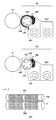
プリンタ3の画像形成部10は画像情報に応じたトナー画像をシートPに形成する電子写真方式の画像形成エンジンである。画像形成部10は、Y(イエロー)、M(マゼンタ)、C(シアン)、Bk(ブラック)の各色のトナー画像を形成する四つのステーションを有している。なお、本発明は単色画像を形成するモノクロプリンタにも適用可能である。図1が示すように、画像形成部10は左側から順にY、M、C、Bkの各色に対応した4つの感光ドラム11を備えている。各感光ドラム11の周囲にはローラ状の帯電器12、露光器13、現像器14、一次転写器17、ドラムクリーナ15などが配置される。以下では、四つの色を代表してBk色のトナー画像を形成する手順が説明される。他色のトナー画像を形成する手順も同様である The image forming unit 10 of the printer 3 is an electrophotographic image forming engine that forms a toner image according to image information on the sheet P. The image forming unit 10 has four stations that form toner images of Y (yellow), M (magenta), C (cyan), and Bk (black). The present invention can also be applied to a monochrome printer that forms a monochrome image. As shown in FIG. 1, the image forming unit 10 includes four photosensitive drums 11 corresponding to the colors Y, M, C, and Bk in order from the left side. Around each photosensitive drum 11, a roller-shaped charger 12, an exposure device 13, a developing device 14, a primary transfer device 17, a drum cleaner 15, and the like are arranged. In the following, a procedure for forming a Bk toner image on behalf of four colors will be described. The procedure for forming toner images of other colors is similar .

画像形成が開始されると、感光ドラム11は矢印方向に回転する。帯電器12は感光ドラム11の表面を均一に帯電させる。露光器13は、プリンタ制御部29が出力される画像情報に応じて感光ドラム11の表面を露光し、静電潜像を形成する。現像器14は静電潜像にトナーを付着させて現像し、トナー画像を形成する。一次転写器17は感光ドラム11に担持されているトナー画像を中間転写ベルト31に一次転写する。中間転写ベルトは三つのローラ34、36、37に吊架されている。ドラムクリーナ15は感光ドラム11に残ったトナーを除去する。これにより感光ドラム11は次の画像を形成可能な状態となる。   When image formation is started, the photosensitive drum 11 rotates in the arrow direction. The charger 12 uniformly charges the surface of the photosensitive drum 11. The exposure device 13 exposes the surface of the photosensitive drum 11 according to the image information output by the printer control unit 29 to form an electrostatic latent image. The developing device 14 attaches toner to the electrostatic latent image and develops the electrostatic latent image to form a toner image. The primary transfer device 17 primarily transfers the toner image carried on the photosensitive drum 11 onto the intermediate transfer belt 31. The intermediate transfer belt is suspended by three rollers 34, 36 and 37. The drum cleaner 15 removes the toner remaining on the photosensitive drum 11. As a result, the photosensitive drum 11 is ready to form the next image.

一方、レジストローラ対26は、給送カセット20又はマルチ給送トレイ30から給紙されたシートPを一旦止めて、シートPを搬送方向と平行となるように斜行補正する。さらに、レジストローラ対26は、中間転写ベルト31上のトナー画像と同期を取ってシートPを中間転写ベルト31と二次転写器27との間に送り込む。二次転写器27は中間転写ベルト31上のトナー画像をシートPに二次転写する。転写クリーナ35は中間転写ベルト31上に残ったトナーを除去する。これにより中間転写ベルト31は次の画像を形成可能な状態となる。定着器40はシートPに対してトナー画像を定着させる。感光ドラム11、帯電器12およびドラムクリーナ15はプロセスカートリッジ50として一体化されている。   On the other hand, the registration roller pair 26 temporarily stops the sheet P fed from the feeding cassette 20 or the multi-feed tray 30 and corrects the skew of the sheet P so that it is parallel to the conveying direction. Further, the registration roller pair 26 sends the sheet P between the intermediate transfer belt 31 and the secondary transfer device 27 in synchronization with the toner image on the intermediate transfer belt 31. The secondary transfer device 27 secondarily transfers the toner image on the intermediate transfer belt 31 onto the sheet P. The transfer cleaner 35 removes the toner remaining on the intermediate transfer belt 31. As a result, the intermediate transfer belt 31 is ready to form the next image. The fixing device 40 fixes the toner image on the sheet P. The photosensitive drum 11, the charger 12, and the drum cleaner 15 are integrated as a process cartridge 50.

[帯電方式]
ここで、帯電器12について詳しく説明する。一般に、帯電方式として、非接触帯電方式と接触式帯電方式の2種類がある。非接触帯電方式は、金属ワイヤなどに高圧電圧を印加することで発生するコロナ放電により帯電を実現する方式である。しかし、コロナ放電は、オゾンや酸化窒素(NOx)などの放電生成物を発生させ、感光ドラム11の劣化や画像ボケの原因となる。また、放電生成物が金属ワイヤに付着すると、放電の不均一が発生し、画像に帯電不良が発生しうる。このため、定期的に金属ワイヤが清掃部材などで清掃される必要がある。接触帯電方式は、帯電器12の帯電部材を感光ドラム11に接触させて帯電処理を行う方式である。一般に、接触帯電方式の方が非接触帯電方式よりも印加電圧が低く、オゾンや酸化窒素(NOx)などの放電生成物の発生が非常に少ない。しかし、ドラムクリーナ15をすり抜けてきたトナーやトナー外添剤が帯電部材に付着や融着すると、帯電不良が発生しうる。
[Charging method]
Here, the charger 12 will be described in detail. Generally, there are two types of charging methods, a non-contact charging method and a contact charging method. The non-contact charging method is a method for realizing charging by corona discharge generated by applying a high voltage to a metal wire or the like. However, the corona discharge generates discharge products such as ozone and nitric oxide (NOx), which causes deterioration of the photosensitive drum 11 and image blur. Further, if the discharge product adheres to the metal wire, the discharge becomes non-uniform, and the image may be defectively charged. Therefore, it is necessary to regularly clean the metal wire with a cleaning member or the like. The contact charging method is a method in which the charging member of the charger 12 is brought into contact with the photosensitive drum 11 to perform the charging process. Generally, the applied voltage is lower in the contact charging method than in the non-contact charging method, and the generation of discharge products such as ozone and nitrogen oxide (NOx) is very small. However, if the toner or toner external additive that has slipped through the drum cleaner 15 adheres to or is fused to the charging member, charging failure may occur.

[交換部品]
本実施例では、感光ドラム11、帯電器12およびドラムクリーナ15を一つのプロセスカートリッジ50に一体化されている。プロセスカートリッジ50を交換することで、感光ドラム11、帯電器12およびドラムクリーナ15を速やかに交換すること可能となる。接触帯電方式は非接触帯電方式よりも帯電器12を小型化することが可能である。本実施例では帯電器12がプロセスカートリッジ50に内蔵されるため、接触帯電方式が採用されている。本実施例では現像器14が画像形成装置1に対して容易に脱着可能である。本実施例では少なくとも一次転写器17と中間転写ベルト31が転写ユニットを形成している。転写ユニットも画像形成装置1に対して容易に脱着可能な構成である。従って、転写ユニットを交換することで、一次転写器17と中間転写ベルト31を速やかに交換することが可能である。このように、プロセスカートリッジ50、現像器14および転写ユニットを交換部品とすることで、ユーザおよびサービスマンによるメンテナンスの平易化とメンテナンス時間の短縮化が実現される。転写クリーナ35も画像形成装置1に対して容易に脱着可能であってもよい。
[Replacement parts]
In this embodiment, the photosensitive drum 11, the charger 12, and the drum cleaner 15 are integrated into one process cartridge 50. By replacing the process cartridge 50, the photosensitive drum 11, the charger 12, and the drum cleaner 15 can be replaced quickly. The contact charging method can make the charger 12 smaller than the non-contact charging method. In this embodiment, since the charger 12 is built in the process cartridge 50, the contact charging method is adopted. In this embodiment, the developing device 14 can be easily attached to and detached from the image forming apparatus 1. In this embodiment, at least the primary transfer device 17 and the intermediate transfer belt 31 form a transfer unit. The transfer unit is also configured to be easily removable from the image forming apparatus 1. Therefore, the primary transfer device 17 and the intermediate transfer belt 31 can be quickly replaced by replacing the transfer unit. As described above, by using the process cartridge 50, the developing device 14, and the transfer unit as replacement parts, the maintenance by the user and the service person can be simplified and the maintenance time can be shortened. The transfer cleaner 35 may also be easily removable from the image forming apparatus 1.

[現像剤]
本実施例で使用される現像剤は非磁性トナーと低磁化高抵抗キャリアで構成される二成分現像剤である。非磁性トナーは、スチレン系樹脂やポリエステル樹脂等の結着樹脂、カーボンブラックや染料、顔料等の着色剤、ワックス等の離型剤、荷電制御剤等を適当量用いることにより構成される。このような非磁性トナーは、粉砕法や重合法なとどの方法により製造される。磁性キャリアとしては、既知のものを使用可能である。例えば、樹脂中に磁性材料としてマグネタイトを分散し、導電化及び抵抗調整のためにカーボンブラックを分散して形成した樹脂キャリアも用いられる。また、フェライト等のマグネタイト単体表面を酸化、還元処理して抵抗調整を行ったものも用いられる。また、フェライト等のマグネタイト単体表面樹脂でコーティングし抵抗調整を行ったものなども用いられる。
[Developer]
The developer used in this embodiment is a two-component developer composed of a non-magnetic toner and a low-magnetization high-resistance carrier. The non-magnetic toner is constituted by using an appropriate amount of a binder resin such as a styrene resin or a polyester resin, a coloring agent such as carbon black, a dye or a pigment, a release agent such as a wax, a charge control agent or the like. Such a non-magnetic toner is manufactured by any method such as a pulverization method or a polymerization method. Known magnetic carriers can be used as the magnetic carrier. For example, a resin carrier formed by dispersing magnetite as a magnetic material in a resin and dispersing carbon black for conductivity and resistance adjustment is also used. Further, a magnetite such as ferrite whose surface is oxidized and reduced to adjust its resistance is also used. Further, a magnetite coated surface resin such as ferrite may be used for resistance adjustment.

[制御システム]
図2は画像形成装置1の制御システムを示している。画像形成装置1はネットワーク123を介して、PC124やサーバ128などのネットワーク機器と接続されている。PCはパーソナルコンピュータの略称である。サーバ128は、たとえば、画像形成装置1のメンテナンスを担当するサービス会社のコンピュータやメールサーバなどである。プリンタ制御部29はイメージリーダー2やプリンタ3を制御するコントローラである。プリンタ制御部29は、画像処理などを担当するプリンタコントローラと、画像形成部10などを制御するエンジン制御とに分かれていてもよい。通信IF55はPC124などから印刷データを受信したり、画像形成装置1から各種のメッセージをPC124やサーバ128に送信したりする通信回路である。IFはインターフェースの略称である。CPU60は画像形成装置1の各部を統括的に制御する制御回路や演算回路である。CPU60は記憶装置63に記憶されている制御プログラムを実行することで各種の機能を実現する。なお、CPU60の機能の一部またはすべてがASICやFPGAなどのハードウエアによって実現されてもよい。ASICは特定用途集積回路の略称である。FPGAはフィールドプログラマブルゲートアレイの略称である。表示装置61は様々な情報を表示するユニットである。入力装置62は様々な情報の入力を受け付けるユニットである。記憶装置63はROMやRAMなどのメモリや、ハードディクスドライブなどの大容量記憶装置を含む。CPU60はイメージリーダー2などから入力された画像データをYMCK形式の画像データに変換し、さらに階調補正などを実行して画像信号を生成し、露光器13に出力する。
[Control system]
FIG. 2 shows a control system of the image forming apparatus 1. The image forming apparatus 1 is connected to network devices such as the PC 124 and the server 128 via the network 123. PC is an abbreviation for personal computer. The server 128 is, for example, a computer or a mail server of a service company in charge of maintenance of the image forming apparatus 1. The printer control unit 29 is a controller that controls the image reader 2 and the printer 3. The printer control unit 29 may be divided into a printer controller that is in charge of image processing and the like, and an engine control that controls the image forming unit 10 and the like. The communication IF 55 is a communication circuit that receives print data from the PC 124 and sends various messages from the image forming apparatus 1 to the PC 124 and the server 128. IF is an abbreviation for interface. The CPU 60 is a control circuit or an arithmetic circuit that comprehensively controls each unit of the image forming apparatus 1. The CPU 60 realizes various functions by executing the control program stored in the storage device 63. Note that some or all of the functions of the CPU 60 may be realized by hardware such as ASIC and FPGA. ASIC is an abbreviation for an application specific integrated circuit. FPGA is an abbreviation for field programmable gate array. The display device 61 is a unit that displays various information. The input device 62 is a unit that receives input of various information. The storage device 63 includes a memory such as a ROM and a RAM, and a mass storage device such as a hard disk drive. The CPU 60 converts the image data input from the image reader 2 or the like into image data in the YMCK format, further executes gradation correction or the like to generate an image signal, and outputs the image signal to the exposure device 13.

CPU60は様々な機能を実現するが、ここでは本実施例に関与する代表的な機能について説明する。チャート生成部64は、交換部品を特定するためのテスト画像をシートP上に形成するよう、プリンタ3を制御する。テスト画像自体またはテスト画像が形成されたシートPはテストチャートまたは単にチャートと呼ばれる。帯電制御部65は帯電器12に印加される帯電電圧を帯電電源68に生成させる。現像制御部66は現像器14に印加される現像電圧を現像電源69に生成させる。診断部67はイメージリーダー2により読み取られたチャートの読取結果に基づいて交換部品を特定する。なお、ユーザやサービスマンがチャートを目視して交換部品を特定する場合、診断部67は省略されてもよい。   The CPU 60 realizes various functions, but here, typical functions related to the present embodiment will be described. The chart generator 64 controls the printer 3 so as to form a test image on the sheet P for identifying the replacement part. The test image itself or the sheet P on which the test image is formed is called a test chart or simply a chart. The charging controller 65 causes the charging power supply 68 to generate a charging voltage applied to the charger 12. The developing control unit 66 causes the developing power supply 69 to generate a developing voltage applied to the developing device 14. The diagnosis unit 67 identifies the replacement part based on the reading result of the chart read by the image reader 2. The diagnostic unit 67 may be omitted when the user or the service person visually identifies the chart to identify the replacement part.

[チャート]
プロセスカートリッジ50や現像器14などが交換時期を迎えると、画像に縦スジが発生することがある。縦スジとは、シートPの搬送方向と平行に延在する直線状の画像である。従来はスジの原因が露光器13にあるのか、帯電器12にあるのかを判別することができたが、帯電器12にあるのか現像器14にあるのかを判別することができなかった。そこで、本実施例は、帯電器12と現像器14とのどちらを交換すべきかを特定可能なチャートを提供する。このチャートをユーザやサービスマンが目視したり、イメージリーダー2に読み取らせたりすることで、交換部品が特定される。とりわけ、本実施例のチャートは、像担持体の帯電電位がそれぞれ異なる複数の画像形成条件で形成された複数のアナログパターンを含むことを特徴としている。
[chart]
When the process cartridge 50, the developing device 14, and the like are about to be replaced, vertical stripes may occur on the image. The vertical stripe is a linear image extending in parallel with the conveyance direction of the sheet P. Conventionally, it was possible to determine whether the streak is due to the exposure device 13 or the charger 12, but it was not possible to determine whether the streaks were due to the charger 12 or the developing device 14. Therefore, the present embodiment provides a chart capable of specifying which of the charging device 12 and the developing device 14 should be replaced. The replacement part is specified by visually checking this chart by a user or a service person or by causing the image reader 2 to read it. In particular, the chart of the present embodiment is characterized by including a plurality of analog patterns formed under a plurality of image forming conditions in which the charged potentials of the image carrier are different from each other.

本実施例ではチャートのサイズとしてA3サイズ(幅方向長さ297mm、搬送方向長さ420mm)が採用されるが、これは一例に過ぎない。画像形成装置1に対して通紙可能な最大のサイズが選択されると、たとえば、帯電器12や現像器14において副走査方向の端部に生じたスジも検出可能となろう。このように、画像形成装置1で印刷可能な最大サイズのシートが採用されれば、交換備品を精度良く特定することが可能となろう。なお、チャートの枚数は1枚であってもよいし、複数枚であってもよい。   In this embodiment, the chart size is A3 size (width-direction length 297 mm, conveyance-direction length 420 mm), but this is only an example. If the maximum size that allows the sheet to pass through the image forming apparatus 1 is selected, for example, it is possible to detect a streak generated at the end of the charging device 12 and the developing device 14 in the sub-scanning direction. In this way, if the maximum size sheet that can be printed by the image forming apparatus 1 is adopted, it will be possible to accurately identify the replacement equipment. The number of charts may be one or may be plural.

図3は例示的なチャート70を示している。チャート70には画像パターンが形成されない白地領域Wと、デジタルパターンDと、2種類のアナログパターンA1、A2が含まれている。なお、参照符号の末尾に付与されているYMCKは、各パターンを形成するために使用されるトナーの色を示している。各パターンを形成する際に使用されるトナーの色は単色であり、YMCKのいずれか一色である。これは、交換されるべき部品がどの色のステーションに存在するかを特定するためである。各パターンの搬送方向の長さは、たとえば、30mm程度である。これは、パターンの長さが30mm程度以上であれば、縦スジの検出が可能だからである。なお、感光ドラム11の外径は30mmであり、その外周は約94.2mmであると仮定されている。   FIG. 3 shows an exemplary chart 70. The chart 70 includes a white background area W in which an image pattern is not formed, a digital pattern D, and two types of analog patterns A1 and A2. Note that YMCK added to the end of the reference numeral indicates the color of the toner used to form each pattern. The color of the toner used when forming each pattern is a single color and is any one of YMCK. This is to identify in which color station the part to be replaced is located. The length of each pattern in the transport direction is, for example, about 30 mm. This is because vertical stripes can be detected if the pattern length is about 30 mm or more. It is assumed that the outer diameter of the photosensitive drum 11 is 30 mm and the outer circumference thereof is about 94.2 mm.

デジタルパターンDの主走査方向の長さは画像形成装置1で形成可能な全域の長さよりは若干短く、デジタルパターンDの主走査方向の両端には余白領域が設けられている。一方、アナログパターンA1、A2の主走査方向の長さはシートPの主走査方向の長さと同じであり、余白は形成されない。   The length of the digital pattern D in the main scanning direction is slightly shorter than the length of the entire area that can be formed by the image forming apparatus 1, and blank areas are provided at both ends of the digital pattern D in the main scanning direction. On the other hand, the length of the analog patterns A1 and A2 in the main scanning direction is the same as the length of the sheet P in the main scanning direction, and no margin is formed.

図10が示すように、4つのデジタルパターンDは露光器13により露光されて形成された露光像(トナー画像)である。アナログパターンA1は、露光器13による露光が実行されず、帯電器12による感光ドラム11の帯電電位が第一帯電電位に設定されて形成された非露光像(トナー画像)である。アナログパターンA2は、露光器13による露光が実行されず、帯電器12による感光ドラム11の帯電電位が第一帯電電位よりも低い第二帯電電位に設定されて形成された非露光像(トナー画像)である。なお、ここでの「高い」や「低い」という用語は絶対値での電位における高低を意味している。帯電器12が原因となるスジと現像器14が原因となるスジの出現の仕方は、アナログパターンA1とアナログパターンA2との間で異なる。つまり、アナログパターンA1に発生したスジとアナログパターンA2に発生したスジとを比較すれば、スジの原因が帯電器12にあるのか現像器14にあるのかが判別可能である。   As shown in FIG. 10, the four digital patterns D are exposure images (toner images) formed by being exposed by the exposure device 13. The analog pattern A1 is a non-exposed image (toner image) formed by the exposure unit 13 not performing the exposure and the charging unit 12 setting the charging potential of the photosensitive drum 11 to the first charging potential. The analog pattern A2 is a non-exposed image (toner image) formed by the exposure unit 13 not performing the exposure and the charging unit 12 setting the charging potential of the photosensitive drum 11 to the second charging potential lower than the first charging potential. ). Note that the terms “high” and “low” here mean high and low in potential in absolute value. The appearance of the streak caused by the charging device 12 and the streak caused by the developing device 14 are different between the analog pattern A1 and the analog pattern A2. That is, by comparing the streak generated in the analog pattern A1 with the streak generated in the analog pattern A2, it is possible to determine whether the cause of the streak is in the charger 12 or the developing device 14.

図4(A)はデジタルパターンDを形成する際に帯電器12によって帯電した感光ドラム11上における各主走査位置における電位を示している。図4(B)はシートPに形成されるデジタルパターンDの濃度d1と白地部Wの濃度d0を示している。濃度d0はシートPの下地(白地)の光学濃度である。   FIG. 4A shows the potential at each main scanning position on the photosensitive drum 11 charged by the charger 12 when the digital pattern D is formed. FIG. 4B shows the density d1 of the digital pattern D and the density d0 of the white background W formed on the sheet P. The density d0 is the optical density of the base (white background) of the sheet P.

帯電制御部65は、感光ドラム11の表面における帯電電位がVd_Dになるように帯電電源68を制御し、帯電器12に感光ドラム11を帯電させる。露光器13は、チャート生成部64により生成された画像データにしたがって感光ドラム11の表面を露光する。その結果、感光ドラム11の表面のうち露光された部分の電位がVl_Dに変化する。現像制御部66は現像器14の現像スリーブの電位が現像バイアスである直流電位Vdc_Dとなるように現像電源69を制御する。Vdc_Dは、帯電電位Vd_Dと露光部の電位Vl_Dとの間に設定される。デジタルパターンDの両端に設けられた余白mは露光されない。そのため、余白mの電位はVd_Dに維持される。このように非露光部である余白mにはかぶりとり電圧Vbが形成される。かぶりとり電圧Vbにより、余白mにはトナーが付着しないようになる。デジタルパターンDの画像信号値は50%に設定される。これは光学濃度で0.6の画像に相当する(つまり、d1=0.6)。このような中間調のパターンはベタのパターンよりも縦スジの検出精度が高くなるからである。   The charging controller 65 controls the charging power source 68 so that the charging potential on the surface of the photosensitive drum 11 becomes Vd_D, and causes the charger 12 to charge the photosensitive drum 11. The exposure device 13 exposes the surface of the photosensitive drum 11 according to the image data generated by the chart generation unit 64. As a result, the potential of the exposed portion of the surface of the photosensitive drum 11 changes to Vl_D. The developing control unit 66 controls the developing power source 69 so that the potential of the developing sleeve of the developing device 14 becomes the DC potential Vdc_D which is the developing bias. Vdc_D is set between the charging potential Vd_D and the potential Vl_D of the exposed portion. The margins m provided at both ends of the digital pattern D are not exposed. Therefore, the potential of the blank space m is maintained at Vd_D. Thus, the fog-removing voltage Vb is formed in the margin m which is the non-exposed portion. The fogging voltage Vb prevents toner from adhering to the margin m. The image signal value of the digital pattern D is set to 50%. This corresponds to an image with an optical density of 0.6 (that is, d1=0.6). This is because such a halftone pattern has a higher vertical stripe detection accuracy than a solid pattern.

図4(C)は第一のアナログパターンA1を形成する際に帯電器12によって帯電した感光ドラム11上における各主走査位置における電位を示している。図4(D)はシートPに形成されるアナログパターンA1の濃度d1を示している。アナログパターンA1を形成すべく、チャート生成部64からの指示に従って帯電制御部65は帯電電源68を制御し、感光ドラム11の表面の電位が帯電電位Vd_A1に調整される。チャート生成部64からの指示に従って現像制御部66は現像電源69を制御し、現像器14の現像スリーブの電位を現像バイアスVdc_A1に調整する。現像バイアスVdc_A1は帯電電位Vd_A1よりも高い現像電位である。なお、チャート生成部64は露光器13にレーザ光の照射を行わせない。これにより、感光ドラム11と現像スリーブとの間には電位差として現像電圧Vc_A1が形成される。つまり、アナログパターンA1に対応した静電潜像が形成され、現像器14から供給されたトナーにより感光ドラム11上にトナー画像が形成される。図4(C)が示すように、アナログパターンA1では、露光が適用されないため、主走査位置によらず一定の現像電圧Vc_A1が形成される。よって、アナログパターンA1の両端には余白が形成されない。また、露光が適用されないため中間調処理を行うことはできない。そこで、本実施例では、アナログパターンA1の各色の光学濃度が0.6になるように、現像制御部66が現像電源69を制御して現像電圧Vc_A1を調整する。図4(D)が示すように、シートPには光学濃度d1(=0.6)のアナログパターンA1が形成される。   FIG. 4C shows the potential at each main scanning position on the photosensitive drum 11 charged by the charger 12 when forming the first analog pattern A1. FIG. 4D shows the density d1 of the analog pattern A1 formed on the sheet P. In order to form the analog pattern A1, the charging controller 65 controls the charging power source 68 according to the instruction from the chart generator 64, and the surface potential of the photosensitive drum 11 is adjusted to the charging potential Vd_A1. The development controller 66 controls the developing power source 69 according to the instruction from the chart generator 64, and adjusts the potential of the developing sleeve of the developing device 14 to the developing bias Vdc_A1. The developing bias Vdc_A1 is a developing potential higher than the charging potential Vd_A1. The chart generation unit 64 does not cause the exposure device 13 to emit the laser light. As a result, the developing voltage Vc_A1 is formed as a potential difference between the photosensitive drum 11 and the developing sleeve. That is, an electrostatic latent image corresponding to the analog pattern A1 is formed, and a toner image is formed on the photosensitive drum 11 by the toner supplied from the developing device 14. As shown in FIG. 4C, in the analog pattern A1, since the exposure is not applied, the constant developing voltage Vc_A1 is formed regardless of the main scanning position. Therefore, no margin is formed at both ends of the analog pattern A1. Further, since exposure is not applied, halftone processing cannot be performed. Therefore, in this embodiment, the developing control unit 66 controls the developing power source 69 to adjust the developing voltage Vc_A1 so that the optical density of each color of the analog pattern A1 becomes 0.6. As shown in FIG. 4D, the analog pattern A1 having the optical density d1 (=0.6) is formed on the sheet P.

図4(E)は第二のアナログパターンA2を形成する際に帯電器12によって帯電した感光ドラム11上における各主走査位置における電位を示している。図4(F)はシートPに形成されるアナログパターンA2の濃度d1を示している。アナログパターンA2を形成すべく、チャート生成部64からの指示に従って帯電制御部65は帯電電源68を制御し、感光ドラム11の表面の電位が帯電電位Vd_A2に調整される。チャート生成部64からの指示に従って現像制御部66は現像電源69を制御し、現像器14の現像スリーブの電位が現像バイアスVdc_A2に調整される。現像バイアスVdc_A2は帯電電位Vd_A2よりも高い電位である。なお、チャート生成部64は露光器13にレーザ光の照射を行わせない。これにより、感光ドラム11と現像スリーブとの間には現像電圧Vc_A2が形成される。つまり、アナログパターンA2に対応した静電潜像が形成され、現像器14から供給されたトナーにより感光ドラム11上にトナー画像が形成される。図4(E)が示すように、アナログパターンA2では、露光が適用されないため、主走査位置によらず一定の現像電圧Vc_A2が形成される。よって、アナログパターンA2の両端には余白が形成されない。また、露光が適用されないため中間調処理を行うことはできない。そこで、本実施例では、アナログパターンA2の各色の光学濃度が0.6になるように、現像制御部66が現像電源69を制御して現像電圧Vc_A2を調整する。図4(F)が示すように、シートPには光学濃度d1(=0.6)のアナログパターンA2が形成される。   FIG. 4E shows the potential at each main scanning position on the photosensitive drum 11 charged by the charger 12 when the second analog pattern A2 is formed. FIG. 4F shows the density d1 of the analog pattern A2 formed on the sheet P. In order to form the analog pattern A2, the charging controller 65 controls the charging power source 68 according to the instruction from the chart generator 64, and the surface potential of the photosensitive drum 11 is adjusted to the charging potential Vd_A2. The development controller 66 controls the developing power source 69 according to the instruction from the chart generator 64, and the potential of the developing sleeve of the developing device 14 is adjusted to the developing bias Vdc_A2. The developing bias Vdc_A2 is higher than the charging potential Vd_A2. The chart generation unit 64 does not cause the exposure device 13 to emit the laser light. As a result, the developing voltage Vc_A2 is formed between the photosensitive drum 11 and the developing sleeve. That is, an electrostatic latent image corresponding to the analog pattern A2 is formed, and a toner image is formed on the photosensitive drum 11 by the toner supplied from the developing device 14. As shown in FIG. 4E, in the analog pattern A2, since the exposure is not applied, the constant developing voltage Vc_A2 is formed regardless of the main scanning position. Therefore, no margin is formed at both ends of the analog pattern A2. Further, since exposure is not applied, halftone processing cannot be performed. Therefore, in this embodiment, the developing control unit 66 controls the developing power source 69 to adjust the developing voltage Vc_A2 so that the optical density of each color of the analog pattern A2 becomes 0.6. As shown in FIG. 4F, the analog pattern A2 having the optical density d1 (=0.6) is formed on the sheet P.

ここで、アナログパターンA2を形成するための第二の帯電電位Vd_A2は、アナログパターンA1を形成するための帯電電位Vd_A1よりも低く設定される(|Vd_A1|>|Vd_A2|)。この結果、アナログパターンA1と比較してアナログパターンA2では、画像エラーに対する帯電器12の寄与率が低減する。なお、現像制御部66は、現像電源69を制御して現像電圧Vc_A1と同じとなるように現像電圧Vc_A2を調整する。これによりアナログパターンA2の各色の光学濃度が0.6になる。   Here, the second charging potential Vd_A2 for forming the analog pattern A2 is set lower than the charging potential Vd_A1 for forming the analog pattern A1 (|Vd_A1|>|Vd_A2|). As a result, in the analog pattern A2, the contribution rate of the charger 12 to the image error is reduced as compared with the analog pattern A1. The developing control unit 66 controls the developing power source 69 to adjust the developing voltage Vc_A2 so that it becomes the same as the developing voltage Vc_A1. As a result, the optical density of each color of the analog pattern A2 becomes 0.6.

なお、非接触帯電方式が用いられる場合、帯電電源68が金属ワイヤに流す電流の量を変えることで、感光ドラム11の帯電電位が調整される。これにより、非接触帯電方式でもアナログパターンA1とアナログパターンA2が形成される。   When the non-contact charging method is used, the charging potential of the photosensitive drum 11 is adjusted by changing the amount of current supplied from the charging power source 68 to the metal wire. Accordingly, the analog pattern A1 and the analog pattern A2 are formed even in the non-contact charging method.

[縦スジ]
図5(A)を用いて、本実施例の画像形成装置1で発生する画像エラーの一つである縦スジについて説明する。図5(A)は縦スジの種類、交換部品または対処方法、白地部の状態、スジが発生するパターンの色、デジタルパターン及びアナログパターンの各々においてスジ発生の有無、アナログパターンにおいて帯電電位を下げた影響を示している。なお、スジが存在しない正常部よりも濃度が薄くなるスジは白スジと呼ばれる。正常部に対して濃度が濃くなるスジは黒スジと呼ばれる。
[Vertical stripes]
A vertical streak, which is one of the image errors that occurs in the image forming apparatus 1 according to the present exemplary embodiment, will be described with reference to FIG. FIG. 5(A) shows the type of vertical stripes, replacement parts or countermeasures, the state of the white background, the color of the pattern in which stripes occur, the presence or absence of stripes in each of the digital pattern and the analog pattern, and the charging potential in the analog pattern is lowered. It shows the impact. A streak whose density is lower than that of a normal part where no streak exists is called a white streak. A streak whose density is higher than that of a normal part is called a black streak.

●現像コート不良に起因したスジ
図5(A)が示す現像コート不良スジとは、現像コートが不十分で発生する縦スジである。図6(A)および図6(B)は現像コート不良に起因したスジが発生する要因を説明する図である。現像コートとは現像スリーブ142の表面に現像剤を均一の厚さで付着させることをいう。現像スリーブ142の内部には現像剤担持体として機能するマグネット141が設けられている。現像スリーブ142は回転自在に現像容器143に支持されている。最近接部145は現像スリーブ142と感光ドラム11との距離が最も近い部分である。現像スリーブ142の回転方向において最近接部145よりも上流側に規制ブレード146が設けられている。規制ブレード146は、現像スリーブ142に対する距離が一定となるように配置されており、最近接部145に供給される二成分現像剤の量を規制する。
● Streaks caused by defective development coat The defective development coat streaks shown in FIG. 5A are vertical streaks caused by insufficient development coat. FIG. 6A and FIG. 6B are diagrams for explaining the factors that cause streaks due to defective development coat. The development coat means that the developer is attached to the surface of the development sleeve 142 with a uniform thickness. Inside the developing sleeve 142, a magnet 141 that functions as a developer carrying member is provided. The developing sleeve 142 is rotatably supported by the developing container 143. The closest portion 145 is a portion where the distance between the developing sleeve 142 and the photosensitive drum 11 is the shortest. A regulating blade 146 is provided on the upstream side of the closest portion 145 in the rotation direction of the developing sleeve 142. The regulation blade 146 is arranged so that the distance to the developing sleeve 142 is constant, and regulates the amount of the two-component developer supplied to the closest portion 145.

図6(B)が示すように、ホコリや髪の毛などの異物148が現像スリーブ142と規制ブレード146との間に詰まることがある。この場合、異物148が現像剤の流れを妨げてしま。図6(C)が示すように、現像スリーブ142上に現像剤が担持されない縦スジ151が発生する。縦スジ151には現像剤が存在しないため、感光ドラム11の表面のうち縦スジ151に対向する部分には現像剤が供給されない。よって感光ドラム11の表面には一直線の連続する縦スジ152が発生する。図5(A)が示すように、このような現像コート不良スジを解消するために交換すべきユニットは現像器14である。 As shown in FIG. 6B, foreign matter 148 such as dust or hair may be clogged between the developing sleeve 142 and the regulation blade 146. In this case, the foreign matter 148 intends want to interfere with the flow of the developer. As shown in FIG. 6C, vertical stripes 151 on which the developer is not carried occur on the developing sleeve 142. Since no developer is present on the vertical stripe 151, the developer is not supplied to the portion of the surface of the photosensitive drum 11 that faces the vertical stripe 151. Therefore, a straight continuous vertical stripe 152 is generated on the surface of the photosensitive drum 11. As shown in FIG. 5A, the developing unit 14 is a unit to be replaced in order to eliminate such a defective development coat streak.

さらに、図5(A)を用いて、現像コートの不良で発生する白スジの特徴を説明する。まず、画像パターンが形成されない白地部Wにはスジが発生しない。そして、スジが発生する色は、現像コート不良が起こった現像器の色のみである。   Further, the features of white streaks caused by defective development coat will be described with reference to FIG. First, no streak is generated in the white background portion W where the image pattern is not formed. Then, the only color in which streaks occur is the color of the developing device in which the development coat defect has occurred.

図7(A)はデジタルパターンDを形成したときの感光ドラム11の各主走査位置における電位を示している。図7(B)はデジタルパターンDを形成したときのシートPの各主走査位置における光学濃度を示している。図7(C)はアナログパターンA1を形成したときの感光ドラム11の各主走査位置における電位を示している。図7(D)はアナログパターンA1を形成したときのシートPの各主走査位置における光学濃度を示している。図7(E)はアナログパターンA2を形成したときの感光ドラム11の各主走査位置における電位を示している。図7(F)はアナログパターンA2を形成したときのシートPの各主走査位置における光学濃度を示している。これらが示すように、現像コート不良スジは現像スリーブ142上に現像剤が供給されないことに起因する。したがって、デジタルパターンD、アナログパターンA1およびアナログパターンA2のすべてで縦スジが発生する。さらに、アナログパターンA1に発生するスジの濃度とアナログパターンA2に発生するスジの濃度に差はない。   FIG. 7A shows the potential at each main scanning position of the photosensitive drum 11 when the digital pattern D is formed. FIG. 7B shows the optical density at each main scanning position of the sheet P when the digital pattern D is formed. FIG. 7C shows the potential at each main scanning position of the photosensitive drum 11 when the analog pattern A1 is formed. FIG. 7D shows the optical density at each main scanning position of the sheet P when the analog pattern A1 is formed. FIG. 7E shows the potential at each main scanning position of the photosensitive drum 11 when the analog pattern A2 is formed. FIG. 7F shows the optical density at each main scanning position of the sheet P when the analog pattern A2 is formed. As shown by these, the defective development coat streak is caused by the fact that the developer is not supplied onto the developing sleeve 142. Therefore, vertical stripes occur in all of the digital pattern D, the analog pattern A1, and the analog pattern A2. Further, there is no difference between the density of streaks generated in the analog pattern A1 and the density of streaks generated in the analog pattern A2.

●露光不良に起因したスジ
次に、図5(A)に示した露光不良に起因した白スジについて説明する。図8(A)は露光不良に起因した白スジの発生メカニズムを説明する図である。露光器13から出力されるレーザ光が通過する光路には防塵ガラス132が設けられている。防塵ガラス132の一部に髪の毛やトナーなどの異物135が付着すると、感光ドラム11の表面に照射されるレーザ光が遮られてしまう。つまり、感光ドラム11の表面のうち異物135によってレーザ光が照射されなかった部分の静電潜像の電位が低下し、縦スジが発生する。この縦スジは、トナーの付着量が減少することで発生するため、白スジとなる。露光不良に起因した白スジを低減するための対処方法は、防塵ガラス132の清掃作業を行うか、露光器13を交換することである。
Streaks Due to Poor Exposure Next, white streaks due to poor exposure shown in FIG. 5A will be described. FIG. 8A is a diagram for explaining the mechanism of white streak generation due to exposure failure. A dustproof glass 132 is provided in the optical path through which the laser light output from the exposure device 13 passes. If foreign matter 135 such as hair or toner adheres to part of the dust-proof glass 132, the laser light emitted to the surface of the photosensitive drum 11 is blocked. That is, the potential of the electrostatic latent image on the surface of the photosensitive drum 11 which is not irradiated with the laser beam due to the foreign matter 135 is lowered, and vertical stripes are generated. The vertical streaks are white streaks because they occur when the amount of adhered toner decreases. A coping method for reducing white streaks caused by poor exposure is to clean the dustproof glass 132 or replace the exposure device 13.

図5(A)を用いて露光不良に起因した白スジの特徴を説明する。まず、画像パターンが形成されない白地部Wにはスジが発生しない。そして、デジタルパターンDにおいてスジが発生する色は、露光不良の起こった露光器13が担当している色である。   The features of white streaks caused by poor exposure will be described with reference to FIG. First, no streak is generated in the white background portion W where the image pattern is not formed. The color in which streaks occur in the digital pattern D is the color that the exposure device 13 in which the exposure failure has occurred is in charge.

図9(A)はデジタルパターンDを形成したときの感光ドラム11の各主走査位置における電位を示している。図9(B)はデジタルパターンDを形成したときのシートPの各主走査位置における光学濃度を示している。図9(C)はアナログパターンA1を形成したときの感光ドラム11の各主走査位置における電位を示している。図9(D)はアナログパターンA1を形成したときのシートPの各主走査位置における光学濃度を示している。図9(E)はアナログパターンA2を形成したときの感光ドラム11の各主走査位置における電位を示している。図9(F)はアナログパターンA2を形成したときのシートPの各主走査位置における光学濃度を示している。   FIG. 9A shows the potential at each main scanning position of the photosensitive drum 11 when the digital pattern D is formed. FIG. 9B shows the optical density at each main scanning position of the sheet P when the digital pattern D is formed. FIG. 9C shows the potential at each main scanning position of the photosensitive drum 11 when the analog pattern A1 is formed. FIG. 9D shows the optical density at each main scanning position of the sheet P when the analog pattern A1 is formed. FIG. 9E shows the potential at each main scanning position of the photosensitive drum 11 when the analog pattern A2 is formed. FIG. 9F shows the optical density at each main scanning position of the sheet P when the analog pattern A2 is formed.

図9(A)や図9(B)が示すように、白スジは露光不良(露光光量が少なくなること)が原因で発生する。このため、デジタルパターンDでは、感光ドラム11の主走査位置の一部において表面電位がVl_Dよりも高くなることで白スジが発生する。一方、図9(C)ないし図9(F)が示すように、アナログパターンA1、A2は露光が適用されずに形成されるため、スジが発生しない。   As shown in FIGS. 9(A) and 9(B), white streaks are caused by defective exposure (reduction in the amount of exposure light). For this reason, in the digital pattern D, a white stripe occurs due to the surface potential being higher than Vl_D at a part of the main scanning position of the photosensitive drum 11. On the other hand, as shown in FIGS. 9C to 9F, since the analog patterns A1 and A2 are formed without exposure, no stripes are generated.

●帯電不良に起因したスジ
本実施例の帯電器12は帯電部材を感光ドラム11に接触させて帯電を行う接触帯電方式を採用している。接触帯電方式では、感光ドラム11の表面のうち主走査方向のある位置でクリーニングが不十分となることで、シリコンなどの外添剤が帯電部材に付着しうる。図10(A)は感光ドラム11の表面電位(帯電電位)を示す図である。図10(B)は画像信号と光学濃度との関係を示す図である。図10(A)が示すように、感光ドラム11の表面のうち一部の主走査位置において帯電部材の抵抗が大きくなり、その位置の帯電電位が高くなる。抵抗が大きくなった主走査領域は高抵抗化部と呼ばれる。帯電電位が高くなると、図10(B)が示すように、感光ドラム11の各主走査位置を同じ画像信号を用いて露光しても、高抵抗化部の濃度は正常部の濃度よりも低くなり、白スジが発生する。
Streaks Due to Poor Charging The charger 12 of the present embodiment employs a contact charging method in which a charging member is brought into contact with the photosensitive drum 11 to perform charging. In the contact charging method, cleaning is insufficient at a certain position in the main scanning direction on the surface of the photosensitive drum 11, so that an external additive such as silicon may adhere to the charging member. FIG. 10A is a diagram showing the surface potential (charging potential) of the photosensitive drum 11. FIG. 10B is a diagram showing the relationship between the image signal and the optical density. As shown in FIG. 10A, the resistance of the charging member becomes large at a part of the main scanning position on the surface of the photosensitive drum 11, and the charging potential at that position becomes high. The main scanning area where the resistance is increased is called a high resistance portion. When the charging potential becomes high, as shown in FIG. 10B, even if each main scanning position of the photosensitive drum 11 is exposed using the same image signal, the density of the high resistance portion is lower than that of the normal portion. And white stripes occur.

一方、感光ドラム11の表面のうち一部の主走査位置においてクリーニング不良が発生すると、トナーが帯電部材に付着することがある。帯電部材の表面のうちトナーが付着した部分の抵抗は小さくなる。帯電部材は耐久により徐々に高抵抗化するが、帯電部材の表層が剥れることでも帯電部材の抵抗が部分的に小さくなる。その結果、図10(A)が示すように、一部の主走査領域で部分的に帯電部材の抵抗が小さくなり、帯電電位が低くなる。この部分は低抵抗化部と呼ばれる。帯電電位が低くなると、図10(B)が示すように、感光ドラム11の各主走査位置を同じ画像信号を用いて露光しても、低抵抗化部の濃度は正常部の濃度よりも高くなり、黒スジが発生する。   On the other hand, if cleaning failure occurs at some main scanning positions on the surface of the photosensitive drum 11, toner may adhere to the charging member. The resistance of the portion of the surface of the charging member to which the toner adheres becomes small. The resistance of the charging member gradually increases due to durability, but the resistance of the charging member partially decreases even when the surface layer of the charging member is peeled off. As a result, as shown in FIG. 10A, the resistance of the charging member partially decreases in a part of the main scanning region, and the charging potential decreases. This portion is called a low resistance portion. When the charging potential becomes low, as shown in FIG. 10B, even if each main scanning position of the photosensitive drum 11 is exposed using the same image signal, the density of the low resistance portion is higher than that of the normal portion. And black streaks occur.

図5(A)を用いて帯電不良スジの特徴を説明する。まず、画像パターンが形成されない白地部Wにはスジが発生しない。そして、YMCKのうちスジの発生する色は、帯電不良の起こった帯電器12が担当している色である。   The characteristics of the charging failure streak will be described with reference to FIG. First, no streak is generated in the white background portion W where the image pattern is not formed. The color in which streaks occur in YMCK is the color in charge of the charger 12 in which the charging failure has occurred.

図11(A)はデジタルパターンDを形成したときの感光ドラム11の各主走査位置における電位を示している。図11(B)はデジタルパターンDを形成したときのシートPの各主走査位置における光学濃度を示している。図11(C)はアナログパターンA1を形成したときの感光ドラム11の各主走査位置における電位を示している。図11(D)はアナログパターンA1を形成したときのシートPの各主走査位置における光学濃度を示している。図11(E)はアナログパターンA2を形成したときの感光ドラム11の各主走査位置における電位を示している。図11(F)はアナログパターンA2を形成したときのシートPの各主走査位置における光学濃度を示している。   FIG. 11A shows the potential at each main scanning position of the photosensitive drum 11 when the digital pattern D is formed. FIG. 11B shows the optical density at each main scanning position of the sheet P when the digital pattern D is formed. FIG. 11C shows the potential at each main scanning position of the photosensitive drum 11 when the analog pattern A1 is formed. FIG. 11D shows the optical density at each main scanning position of the sheet P when the analog pattern A1 is formed. FIG. 11E shows the potential at each main scanning position of the photosensitive drum 11 when the analog pattern A2 is formed. FIG. 11F shows the optical density at each main scanning position of the sheet P when the analog pattern A2 is formed.

図11(A)や図11(B)が示すように、デジタルパターンDでは露光された感光ドラム11の一部の主走査位置における帯電電位がVl_Dとは異なる。帯電電位がVl_Dよりも低い位置では黒スジが発生し、帯電電位がVl_Dよりも高い位置では白スジが発生する。図11(C)や図11(D)が示すように、アナログパターンA1でも、主走査方向の一部で帯電電位がVd_A1とは異なるため、黒スジや白スジが発生する。帯電不良は帯電部材の抵抗差に起因して発生するため、帯電器12の帯電電位を低下させすることで帯電不良が低減する。図11(E)や図11(F)が示すように、アナログパターンA2では、アナログパターンA1と比較して、帯電不良の影響が小さくなる。つまり、スジが良化する。スジが良化するとは、スジの光学濃度とその周囲の正常部の光学濃度との差が減少することをいう。つまり、スジが良化すると、視覚的にスジが目立ちにくくなる。   As shown in FIGS. 11A and 11B, in the digital pattern D, the charging potential at a part of the main scanning position of the exposed photosensitive drum 11 is different from Vl_D. Black streaks occur at positions where the charging potential is lower than Vl_D, and white streaks occur at positions where the charging potential is higher than Vl_D. As shown in FIGS. 11C and 11D, even in the analog pattern A1, black stripes and white stripes are generated because the charging potential is different from Vd_A1 in part in the main scanning direction. Since the charging failure occurs due to the resistance difference of the charging member, the charging failure is reduced by lowering the charging potential of the charger 12. As shown in FIGS. 11E and 11F, in the analog pattern A2, the influence of charging failure is smaller than that in the analog pattern A1. That is, the streaks are improved. The improvement of the streak means that the difference between the optical density of the streak and the optical density of the normal part around the streak is reduced. That is, when the streaks are improved, the streaks become less visible visually.

●中間転写ベルトの塑性変形に起因したスジ
次に、図5(A)に示した中間転写ベルト31の塑性変形に起因したスジについて説明する。長期の使用による中間転写ベルト31の内面が削れて粉が発生しうる。転写ユニットを構成する部品の一部などがローラ36、37の表面に付着することがある。図8(B)が示すように、中間転写ベルト31の一部が凸形状に塑性変形する。この部分は凸形状部311と呼ばれる。このように中間転写ベルト31に凸形状部311が発生すると、凸形状部311の両側は感光ドラム11やシートPと接触しにくくなる。よって、両側部分はシートPに対してトナー画像を二次転写しにくくなり、白スジが発生する。凸形状部311はシートPに対して多くのトナーを二次転写するため、黒スジが発生する。よって、中間転写ベルト31の塑性変形によるスジを解消するために交換すべき部品は中間転写ユニットである。なお、白スジとは白色のスジではなく濃度が薄くなる(トナーが少なくなる)淡スジのことである。また、黒スジとは濃度が濃くなる(トナーが多くなる)濃スジのことである。
Streaks Due to Plastic Deformation of Intermediate Transfer Belt Next, streaks due to plastic deformation of the intermediate transfer belt 31 shown in FIG. 5A will be described. The powder may be generated by scraping the inner surface of the intermediate transfer belt 31 due to long-term use. Part of the components that form the transfer unit may adhere to the surfaces of the rollers 36 and 37. As shown in FIG. 8B, a part of the intermediate transfer belt 31 is plastically deformed into a convex shape. This portion is called a convex portion 311. When the convex portion 311 is generated on the intermediate transfer belt 31 in this way, both sides of the convex portion 311 are less likely to come into contact with the photosensitive drum 11 or the sheet P. Therefore, it becomes difficult to secondarily transfer the toner image to the sheet P on both side portions, and white streaks occur. The convex portion 311 secondarily transfers a large amount of toner onto the sheet P, so that black streaks occur. Therefore, the component to be replaced in order to eliminate streaks due to plastic deformation of the intermediate transfer belt 31 is the intermediate transfer unit. The white stripe is not a white stripe but a light stripe whose density is low (toner is reduced). The black streak is a dark streak whose density is high (the amount of toner increases).

図5(A)を用いて塑性変形に起因したスジの特徴を説明する。画像パターンが形成されない白地部Wにはスジが発生しない。YMCKのうちスジの発生する色は全ての色である。なぜなら、このタイプのスジは二次転写部分で発生するためである。また、露光の有無や帯電電位とは無関係であるため、デジタルパターンDだけでなく、アナログパターンA1、A2でもスジが発生する。   Features of streaks caused by plastic deformation will be described with reference to FIG. No streak is generated in the white background portion W where the image pattern is not formed. The colors in which streaks occur in YMCK are all colors. This is because this type of streak occurs in the secondary transcription part. Further, since it is irrelevant to the presence or absence of exposure and the charging potential, streaks are generated not only in the digital pattern D but also in the analog patterns A1 and A2.

●感光ドラムのクリーニング不良に起因したスジ
感光ドラム11のクリーニング不良に起因したスジは黒スジとなる。ドラムクリーナ15のうち、感光ドラム11との当接部材(ブレード)の一部が欠損することがある。この欠損部分は、一次転写後に感光ドラム11上に残ったトナーを掻き取ることができない。これが黒スジの原因となる。このタイプの黒スジは、クリーニング不良が発生したドラムクリーナ15が担当している色で発生する。たとえば、イエローステーションのドラムクリーナ15でクリーニング不良が発生すると、イエローのスジが発生する。また、クリーニング不良にともなう黒スジは白地部Wにほぼ一直線状のスジとして発生する。よって、感光ドラム11のクリーニング不良に伴うスジを低減するために交換すべき部品はプロセスカートリッジ50である。このようにドラムクリーナ15を含むアセンブリユニットが交換部品となる。
Streaks due to poor cleaning of the photosensitive drum Streaks due to poor cleaning of the photosensitive drum 11 are black streaks. In the drum cleaner 15, a part of the abutting member (blade) with the photosensitive drum 11 may be damaged. The defective portion cannot scrape off the toner remaining on the photosensitive drum 11 after the primary transfer. This causes black streaks. This type of black streak occurs in the color that the drum cleaner 15 in which the cleaning failure occurs is in charge. For example, if cleaning failure occurs in the drum cleaner 15 of the yellow station, yellow streaks occur. Further, black streaks due to poor cleaning occur as substantially straight streaks on the white background portion W. Therefore, the process cartridge 50 is a component to be replaced in order to reduce streaks caused by defective cleaning of the photosensitive drum 11. Thus, the assembly unit including the drum cleaner 15 is a replacement part.

図5(A)を用いてクリーニング不良に起因したスジの特徴を説明する。クリーニング不良に起因してスジが発生するため、画像パターンが形成されない白地部Wにもスジが発生する。白地部Wに発生するスジの色は、ドラムクリーナ15に蓄積されたトナーの色と同じ色である。よってこのタイプのスジは単色のスジとなる。スジは画像を形成していない色でも発生するため、イエロー、マゼンタ、シアン、ブラックの全ての色のパターンで発生する。たとえば、イエローを担当するドラムクリーナ15が欠損すると、シートPの副走査方向の全域にわたってイエローのスジが発生するため、すべての色のパターンにスジが発生する。また、露光の有無や帯電電位とは無関係であるため、デジタルパターンD、アナログパターンA1、A2のいずれでもスジが発生する。   Features of streaks caused by defective cleaning will be described with reference to FIG. Since streaks are generated due to poor cleaning, streaks are also generated on the white background portion W where the image pattern is not formed. The color of the streak generated on the white background portion W is the same as the color of the toner accumulated in the drum cleaner 15. Therefore, this type of streak is a monochromatic streak. Since streaks occur even in a color that does not form an image, they occur in patterns of all colors of yellow, magenta, cyan, and black. For example, if the drum cleaner 15 in charge of yellow is missing, yellow streaks are generated over the entire area of the sheet P in the sub-scanning direction, and streaks are generated in the patterns of all colors. Further, since there is no relation to the presence or absence of exposure and the charging potential, streaks are generated in any of the digital pattern D and the analog patterns A1 and A2.

●中間転写ベルトのクリーニング不良に起因したスジ
図5(A)を用いて中間転写ベルト31のクリーニング不良に起因して発生する黒スジについて説明する。転写クリーナ35のうち中間転写ベルト31との当接部材(ブレードなど)の一部が欠損すると、黒スジが発生する。これは二次転写後に中間転写ベルト31上に残存しているトナーを掻き取ることができないために発生する。このタイプのスジの色は、イエロー、マゼンタ、シアン、ブラックの各トナーが混ざった色(混色)となる。よって、中間転写ベルト31のクリーニング不良に起因して発生する黒スジを低減するために交換すべきユニットは転写クリーナ35である。
Streaks Due to Poor Cleaning of Intermediate Transfer Belt Black streaks that occur due to poor cleaning of the intermediate transfer belt 31 will be described with reference to FIG. When a part of a member (a blade or the like) of the transfer cleaner 35 that contacts the intermediate transfer belt 31 is missing, a black streak occurs. This occurs because the toner remaining on the intermediate transfer belt 31 cannot be scraped off after the secondary transfer. The color of this type of streak is a color (mixed color) in which toners of yellow, magenta, cyan, and black are mixed. Therefore, the transfer cleaner 35 is the unit to be replaced in order to reduce the black stripes caused by poor cleaning of the intermediate transfer belt 31.

図5(A)を用いて中間転写ベルト31のクリーニング不良に起因したスジの特徴を説明する。クリーニング不良が原因であるため、画像パターンが形成されない白地部Wにもスジが発生する。そして、白地部Wに発生するスジは転写クリーナ35に蓄積されたトナーによるものなので、スジの色はイエロー、マゼンタ、シアン、ブラックの混色となる。また、露光の有無や帯電電位とは無関係であるため、デジタルパターンD、アナログパターンA1、A2のいずれでもスジが発生する。   The characteristics of streaks caused by poor cleaning of the intermediate transfer belt 31 will be described with reference to FIG. Due to poor cleaning, streaks also occur on the white background portion W where the image pattern is not formed. Since the streak generated on the white background portion W is due to the toner accumulated in the transfer cleaner 35, the color of the streak is a mixed color of yellow, magenta, cyan, and black. Further, since there is no relation to the presence or absence of exposure and the charging potential, streaks are generated in any of the digital pattern D and the analog patterns A1 and A2.

[交換部品の特定処理]
図12を用いて交換部品を特定するためのチャート70の作成処理と交換部品の特定処理が説明される。CPU60は、入力装置62から交換部品の特定指示またはチャート70の作成指示が入力されると、以下の処理を実行する。
[Specifying replacement parts]
The process of creating the chart 70 for identifying the replacement part and the process of identifying the replacement part will be described with reference to FIG. When the instruction to specify the replacement part or the instruction to create the chart 70 is input from the input device 62, the CPU 60 executes the following processing.

S101でCPU60(チャート生成部64)はプリンタ3を制御してシートPに白地部W、デジタルパターンD、アナログパターンA1、A2を形成することで、チャート70を作成する。チャート生成部64は、白地部Wを形成するために帯電器12に所定の帯電電位を設定し、現像器14に所定の現像電位を設定し、かつ、露光器13に発光を禁止する。これにより、シートP(チャート70)に白地部Wが形成される。さらに、チャート生成部64は、デジタルパターンDYを形成するために、イエローステーションの帯電器12に帯電電位Vd_Dを設定する。また、チャート生成部64は、イエローステーションの現像器14に現像電位Vdc_Dを設定する。さらに、チャート生成部64は、イエローステーションの露光器13にデジタルパターンDYを形成するための画像信号を出力する。これにより、デジタルパターンDYが形成される。同様に、デジタルパターンDM、DC、DBkが形成される。次に、CPU60はアナログパターンA1Yを形成するために、各色のステーションの帯電器12に帯電電位Vd_A1を設定する。また、チャート生成部64は、各色のステーションの現像器14に現像電位Vdc_A1を設定する。これにより、アナログパターンA1Y、A1M、A1C、A1Bkが形成される。次に、CPU60はアナログパターンA2Yを形成するために、各色のステーションの帯電器12に帯電電位Vd_A2を設定する。また、チャート生成部64は、各色のステーションの現像器14に現像電位Vdc_A2を設定する。これにより、アナログパターンA2Y、A2M、A2C、A2Bkが形成される。以上によりチャート70が形成され、画像形成装置1の排出トレイに排出される。なお、チャート70をユーザまたはサービスマンが目視により交換部品を特定する場合は、以下の処理が省略される。   In S101, the CPU 60 (chart generation unit 64) controls the printer 3 to form the white background portion W, the digital pattern D, and the analog patterns A1 and A2 on the sheet P, thereby creating the chart 70. The chart generation unit 64 sets a predetermined charging potential in the charger 12 to form the white background W, sets a predetermined developing potential in the developing unit 14, and prohibits the exposure unit 13 from emitting light. As a result, the white background portion W is formed on the sheet P (chart 70). Further, the chart generation unit 64 sets the charging potential Vd_D to the charger 12 of the yellow station in order to form the digital pattern DY. Further, the chart generator 64 sets the developing potential Vdc_D to the developing device 14 of the yellow station. Furthermore, the chart generation unit 64 outputs an image signal for forming the digital pattern DY to the exposure device 13 of the yellow station. As a result, the digital pattern DY is formed. Similarly, digital patterns DM, DC, DBk are formed. Next, the CPU 60 sets the charging potential Vd_A1 to the charger 12 of each color station in order to form the analog pattern A1Y. Further, the chart generation unit 64 sets the development potential Vdc_A1 to the developing device 14 of each color station. As a result, analog patterns A1Y, A1M, A1C, A1Bk are formed. Next, the CPU 60 sets the charging potential Vd_A2 to the charger 12 of each color station in order to form the analog pattern A2Y. Further, the chart generator 64 sets the developing potential Vdc_A2 to the developing device 14 of each color station. As a result, analog patterns A2Y, A2M, A2C, A2Bk are formed. The chart 70 is formed as described above and is discharged to the discharge tray of the image forming apparatus 1. When the user or the service person visually identifies the replacement part on the chart 70, the following processing is omitted.

S102でCPU60(診断部67)はイメージリーダー2を制御し、チャート70を読み取る。診断部67はチャート70を原稿台ガラス22に載置して、読取開始ボタンを押すことを促すガイダンスを表示装置61に表示してもよい。チャート70の読取結果は記憶装置63に格納される。   In S102, the CPU 60 (diagnosis unit 67) controls the image reader 2 to read the chart 70. The diagnosis unit 67 may place the chart 70 on the platen glass 22 and display guidance on the display device 61 to prompt the user to press the reading start button. The reading result of the chart 70 is stored in the storage device 63.

S103でCPU60(診断部67)はチャート70の読取結果からスジを検出する。たとえば、診断部67は読取結果である画像データを解析し、スジを検出するための特徴量を取得してもよい。読取結果にはRGBの輝度値が含まれており、診断部67はR画像、G画像、B画像に読取結果を分割して、色ごとに個別に解析を実行する。つまり、診断部67は、R画像、G画像、B画像の各々の画像データについて縦スジを検出する。なお、診断部67はR画像、G画像、B画像をY画像、M画像、C画像、K画像に変換してから各色について縦スジを検出してもよい。診断部67は、画像データの縦方向(チャート70の搬送方向やイメージリーダー2のスキャン方向)に並んだ複数の画素の輝度値の平均値を演算する。これは、イメージリーダー2で重畳された電気的なノイズを低減するためである。本実施例では各色のパターンの幅(副走査方向の長さ)が30mmであることから、30mmに相当する複数の画素に平均化が適用される。診断部67は、画像データの横方向(縦方向に垂直な方向、主走査方向)に沿って輝度値(縦方向での平均値)の傾きを補正する傾き補正処理を行う。これによりイメージリーダー2や画像パターンの濃度ムラの影響が低減される。診断部67は、画像データにおいて一様な部分(正常部)に対して輝度値の差がある画素群(領域)を検出する。たとえば、診断部67は、画像パターンの全体での平均輝度値と各主走査位置の輝度値(傾き補正された輝度値)との差分(輝度差)を算出する。診断部67は、輝度差が予め定められた閾値(例:平均値の20%)を超える画素群を縦スジとして検出する。診断部67は、正常部の輝度よりも輝度が低い(濃度が高い)スジを黒スジと判別し、逆に輝度が高い(濃度が低い)スジを白スジと判別してもよい。診断部67は、スジが検出された主走査位置および副走査位置、スジの色、輝度差などをスジの特徴量として記憶装置63に格納する。なお、スジの位置は白地部W、デジタルパターンD、アナログパターンA1、A2のどこでスジが発生しているかを示している。スジの色は、交換部品を特定するのに役立つ。アナログパターンA1におけるスジについての輝度差とアナログパターンA2におけるスジについての輝度差はスジが良化しているどうかを判定するのに役立つ。   In S103, the CPU 60 (diagnosis unit 67) detects streaks from the reading result of the chart 70. For example, the diagnosis unit 67 may analyze the image data that is the read result and acquire the feature amount for detecting the streak. The reading result includes RGB brightness values, and the diagnosis unit 67 divides the reading result into R image, G image, and B image, and executes analysis individually for each color. That is, the diagnosis unit 67 detects vertical stripes in each image data of the R image, the G image, and the B image. The diagnosis unit 67 may detect the vertical stripes for each color after converting the R image, the G image, and the B image into the Y image, the M image, the C image, and the K image. The diagnosis unit 67 calculates the average value of the brightness values of a plurality of pixels arranged in the vertical direction of the image data (the conveyance direction of the chart 70 or the scanning direction of the image reader 2). This is to reduce the electrical noise superimposed on the image reader 2. In this embodiment, since the width of each color pattern (length in the sub-scanning direction) is 30 mm, averaging is applied to a plurality of pixels corresponding to 30 mm. The diagnostic unit 67 performs a tilt correction process for correcting the tilt of the brightness value (the average value in the vertical direction) along the horizontal direction (direction perpendicular to the vertical direction, main scanning direction) of the image data. As a result, the influence of the image reader 2 and the uneven density of the image pattern is reduced. The diagnosis unit 67 detects a pixel group (region) having a difference in luminance value with respect to a uniform portion (normal portion) in the image data. For example, the diagnosis unit 67 calculates the difference (luminance difference) between the average luminance value of the entire image pattern and the luminance value of each main scanning position (luminance value after inclination correction). The diagnosis unit 67 detects a pixel group in which the brightness difference exceeds a predetermined threshold value (eg, 20% of the average value) as a vertical stripe. The diagnosis unit 67 may determine streaks having lower luminance (higher density) than the luminance of the normal portion as black streaks, and conversely may determine streaks having higher luminance (lower density) as white streaks. The diagnosis unit 67 stores the main scanning position and the sub-scanning position where the streak is detected, the color of the streak, the brightness difference, and the like in the storage device 63 as the feature amount of the streak. The position of the streak indicates where the streak occurs in the white background portion W, the digital pattern D, and the analog patterns A1 and A2. The color of the streak helps identify the replacement part. The luminance difference for the streak in the analog pattern A1 and the luminance difference for the streak in the analog pattern A2 are useful for determining whether or not the streak is improved.

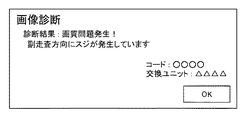
S104でCPU60(診断部67)はチャート70の読取結果(スジの検出結果)に基づきスジの原因と交換部品(または対処方法)を特定する。たとえば、診断部67は記憶装置63に記憶したスジの特徴量に基づき白地部WやYMCKのパターンごとにスジの有無やスジの色(単色(YMCK)/混色など)を判別する。診断部67は、この判別結果と、原因および交換部品を特定するための特定条件とを比較することで、原因および交換部品を特定する。S105でCPU60(診断部67)は交換部品や対処方法を示すメッセージを表示装置61に表示したり、通信IF55を介してPC124やサーバ128に送信したりする。   In S104, the CPU 60 (diagnosis unit 67) identifies the cause of the streak and the replacement part (or the coping method) based on the reading result (the streak detection result) of the chart 70. For example, the diagnosis unit 67 determines the presence/absence of a stripe and the color of the stripe (a single color (YMCK)/mixed color, etc.) for each pattern of the white background portion W and YMCK based on the feature amount of the stripe stored in the storage device 63. The diagnosis unit 67 specifies the cause and the replacement part by comparing the determination result with the specific condition for specifying the cause and the replacement part. In S105, the CPU 60 (diagnosis unit 67) displays a message indicating a replacement part or a coping method on the display device 61 or transmits the message to the PC 124 or the server 128 via the communication IF 55.

図13は交換部品や対処方法を示すメッセージの一例を示している。この例では、チャート70に縦スジ(副走査方向に延在するスジ)が発生していることや、原因を示すコード、交換部品の名称などの情報が含まれている。ユーザやサービスマンはメッセージを参照することで、スジの原因や交換部品を容易に理解することができる。なお、縦スジが検出されなければ、診断部67は画像形成装置1が正常であることを示すメッセージを表示装置61に表示する。このように、具体的な情報で縦スジの発生および交換部品がわかるため、ユーザおよびサービスマン等が交換部品を容易に理解できるようになる。   FIG. 13 shows an example of a message indicating a replacement part and a coping method. In this example, the chart 70 includes information such as vertical streaks (streaks extending in the sub-scanning direction), codes indicating causes, names of replacement parts, and the like. The user or service person can easily understand the cause of the streak and the replacement part by referring to the message. If the vertical stripe is not detected, the diagnosis unit 67 displays a message indicating that the image forming apparatus 1 is normal on the display device 61. As described above, since the generation of the vertical stripes and the replacement part can be known from the specific information, the user and the service person can easily understand the replacement part.

[交換部品の特定処理の詳細]
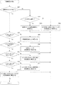
図14は交換部品や対処方法を特定する処理の詳細を示すフローチャートである。CPU60(診断部67)は、主走査位置ごと(例:1mmごと)に縦スジを検出する。このため、複数の主走査位置で縦スジが検出されることもあろう。また、複数の縦ジスの原因がそれぞれ異なることもある。したがって、CPU60(診断部67)はスジごとに原因と交換部品を特定する。なお、スジの発生原因を特定することで、交換部品が特定されてもよい。図14に示した各判定処理は、交換部品や原因を特定するための特定条件の集合体でもある。
[Details of replacement part identification processing]
FIG. 14 is a flowchart showing the details of the process for identifying the replacement part and the coping method. The CPU 60 (diagnosis unit 67) detects a vertical stripe for each main scanning position (for example, every 1 mm). Therefore, vertical stripes may be detected at a plurality of main scanning positions. Further, the causes of the vertical stripes may be different from each other. Therefore, the CPU 60 (diagnosis unit 67) identifies the cause and the replacement part for each stripe. The replacement part may be specified by specifying the cause of the streak. Each determination process shown in FIG. 14 is also a set of specific conditions for specifying replacement parts and causes.

S200でCPU60は記憶装置63から特徴量を読み出し、白地部Wにスジが無いかどうかを判定する。チャート70における白地部Wの座標は既知である。CPU60はスジの位置と白地部Wの座標とを比較することで、白地部Wにおけるスジの有無を判別する。白地部Wにスジが有れば、CPU60はS201に進む。   In S200, the CPU 60 reads the characteristic amount from the storage device 63 and determines whether or not there is a streak in the white background portion W. The coordinates of the white background portion W in the chart 70 are known. The CPU 60 determines the presence/absence of a streak in the white background portion W by comparing the position of the streak with the coordinates of the white background portion W. If there is a streak on the white background portion W, the CPU 60 advances to S201.

S201でCPU60はスジの色が混色かどうかを判定する。スジの色が混色であればCPU60はS202に進む。S202でCPU60は、スジの原因を中間転写ベルト31のクリーニング不良と判別し、転写クリーナ35を交換部品に特定する。一方で、スジの色がYMCKいずれかの単色であればCPU60はS203に進む。S203でCPU60はスジの原因を感光ドラム11のクリーニング不良と判別し、スジの色に対応したプロセスカートリッジ50を交換部品に特定する。S200で白地部Wにおいてスジが検出されなければ、CPU60はS204に進む。   In S201, the CPU 60 determines whether the streak color is a color mixture. If the color of the streak is a mixed color, the CPU 60 advances to S202. In S202, the CPU 60 determines that the cause of the streak is poor cleaning of the intermediate transfer belt 31, and specifies the transfer cleaner 35 as a replacement part. On the other hand, if the color of the streak is a single color of YMCK, the CPU 60 advances to S203. In S203, the CPU 60 determines that the cause of the streak is defective cleaning of the photosensitive drum 11, and identifies the process cartridge 50 corresponding to the streak color as a replacement part. If the streak is not detected in the white background portion W in S200, the CPU 60 proceeds to S204.

S204でCPU60は記憶装置63から特徴量を読み出し、デジタルパターンDY〜DBkにスジが存在するかどうかを判定する。チャート70におけるデジタルパターンDY〜DBkの座標は既知である。CPU60はスジの位置とデジタルパターンDY〜DBkの座標とを比較することで、デジタルパターンDY〜DBkにおけるスジの有無を判別する。デジタルパターンDY〜DBkのいずれにもスジがなければ、CPU60はS205に進む。S205でCPU60は交換部品がない(正常)と特定する。一方で、CPU60はデジタルパターンDY〜DBkのいずれかにスジを検出すると、S206に進む。   In S204, the CPU 60 reads the characteristic amount from the storage device 63 and determines whether or not there are streaks in the digital patterns DY to DBk. The coordinates of the digital patterns DY to DBk on the chart 70 are known. The CPU 60 determines the presence/absence of streaks in the digital patterns DY to DBk by comparing the positions of the streaks with the coordinates of the digital patterns DY to DBk. If there is no streak in any of the digital patterns DY to DBk, the CPU 60 proceeds to S205. In S205, the CPU 60 identifies that there is no replacement part (normal). On the other hand, when the CPU 60 detects a streak in any of the digital patterns DY to DBk, the process proceeds to S206.

S206でCPU60は記憶装置63から特徴量を読み出し、スジが特定色で発生しているかどうかを判定する。これはスジが全色(デジタルパターンDY〜DBkのすべて)で発生しているかどうかを判定することと同じである。スジが全色で発生していれば、CPU60はS207に進む。S207でCPU60はスジの原因を中間転写ベルト31の塑性変形と判別し、中間転写ベルト31を含む転写ユニットを交換部品に特定する。一方で、スジが特定色でのみ発生していれば、CPU60はS208に進む。   In step S206, the CPU 60 reads the characteristic amount from the storage device 63 and determines whether streaks occur in a specific color. This is the same as determining whether streaks occur in all colors (all of the digital patterns DY to DBk). If streaks occur in all colors, the CPU 60 advances to S207. In S207, the CPU 60 determines that the cause of the streak is the plastic deformation of the intermediate transfer belt 31, and specifies the transfer unit including the intermediate transfer belt 31 as a replacement part. On the other hand, if the streak is generated only in the specific color, the CPU 60 proceeds to S208.

S208でCPU60はスジが発生しているデジタルパターンDの色と同じ色のアナログパターンA1にスジが発生しているかどうかを判定する。アナログパターンA1にスジがなければ、CPU60はS209に進む。S209でCPU60は、スジの原因を露光不良と判別し、スジの色に対応した露光器13を交換部品に特定する。なお、CPU60は、スジの色に対応した露光器13の清掃を対処方法として特定してもよい。スジが発生しているデジタルパターンDの色と同じ色のアナログパターンA1にスジが発生していれば、CPU60はS210に進む。   In S208, the CPU 60 determines whether or not there is a streak in the analog pattern A1 of the same color as the color of the digital pattern D in which the streak has occurred. If there is no stripe in the analog pattern A1, the CPU 60 advances to S209. In S209, the CPU 60 determines that the cause of the streak is defective exposure, and specifies the exposure unit 13 corresponding to the streak color as a replacement part. Note that the CPU 60 may specify cleaning of the exposure device 13 corresponding to the color of the streak as a coping method. If there is a streak in the analog pattern A1 of the same color as the color of the digital pattern D in which the streak has occurred, the CPU 60 proceeds to S210.

S210でCPU60はアナログパターンA1のスジに対してアナログパターンA2のスジが良化しているかどうかを判定する。なお、アナログパターンA1とアナログパターンA2は同じ色のものである。たとえば、CPU60は記憶装置63から特徴量を読み出し、アナログパターンA1のスジの輝度差(濃度差)とアナログパターンA2のスジの輝度差(濃度差)を比較してもよい。アナログパターンA2のスジの濃度差がアナログパターンA1のスジの濃度差がよりも小さければ、スジが良化しているため、CPU60はS212に進む。S212でCPU60はスジの原因を帯電不良と判別し、スジの色に対応したプロセスカートリッジ50を交換部品に特定する。一方で、アナログパターンA2のスジがアナログパターンA1のスジと比較して良化していなければ、CPU60はS211に進む。S211でCPU60はスジの原因を現像コート不良と判別し、スジの色に対応した現像器14を交換部品に特定する。   In S210, the CPU 60 determines whether the streak of the analog pattern A2 is better than the streak of the analog pattern A1. The analog pattern A1 and the analog pattern A2 have the same color. For example, the CPU 60 may read the feature amount from the storage device 63 and compare the luminance difference (density difference) of the stripes of the analog pattern A1 with the luminance difference (density difference) of the stripes of the analog pattern A2. If the density difference of the streaks of the analog pattern A2 is smaller than the density difference of the streaks of the analog pattern A1, the streak has been improved, and the CPU 60 proceeds to S212. In S212, the CPU 60 determines that the cause of the streak is defective charging, and identifies the process cartridge 50 corresponding to the streak color as a replacement part. On the other hand, if the stripes of the analog pattern A2 are not improved as compared with the stripes of the analog pattern A1, the CPU 60 proceeds to S211. In S211, the CPU 60 determines the cause of the streak to be a defective development coat, and identifies the developing device 14 corresponding to the streak color as a replacement part.

このようにCPU60はチャート70を作成し、チャート70に発生したスジを分析することでスジの原因と交換部品を特定する。また、CPU60はスジの原因や交換部品を示すメッセージを表示装置61などに出力してもよい。これのより、ユーザやサービスマンがスジの原因や交換部品を容易に認識できるようになる。そのため、メンテナンスに必要な作業時間(ダウンタイム)が大幅に短縮されよう。また、スジに関与した部品が特定されるため、スジに関与していない部品まで交換されることはなくなるであろう。よって、メンテナンス時間に加えてメンテナンスコストも削減されよう。スジの原因や交換部品を示すメッセージはネットワークを介してサービスマンのサーバ128に送信されてもよい。サービスマンは事前に交換部品を把握できるため、交換部品を確実に携帯してメンテナンスを行うことができる。図14に示したスジの原因や交換部品等を特定する処理はユーザやサービスマンがチャート70を目視して実行してもよい。ここでは、カラープリンタが一例として採用されているが、モノクロプリンタに本実施例が適用されてもよい。   In this way, the CPU 60 creates the chart 70 and analyzes the streak generated on the chart 70 to identify the cause of the streak and the replacement part. Further, the CPU 60 may output a message indicating the cause of the streak and the replacement part to the display device 61 or the like. As a result, the user or service person can easily recognize the cause of the streak and the replacement part. Therefore, the work time (downtime) required for maintenance will be greatly reduced. In addition, since the parts involved in the streak are specified, the parts not involved in the streak will not be replaced. Therefore, the maintenance cost will be reduced in addition to the maintenance time. The message indicating the cause of the streak and the replacement part may be transmitted to the serviceman's server 128 via the network. Since the service person can grasp the replacement part in advance, the replacement part can be reliably carried for maintenance. The process of identifying the cause of the streak, the replacement part, and the like shown in FIG. 14 may be executed by the user or a service person by visually observing the chart 70. Although a color printer is adopted here as an example, this embodiment may be applied to a monochrome printer.

図3に示したチャート70は一例に過ぎない。チャート70における白地部W、デジタルパターンD、アナログパターンA1、A2の順序は他の順序であってもよい。要するに、チャート70に白地部W、デジタルパターンD、アナログパターンA1、A2が含まれていれば十分である。とりわけ、スジの原因が帯電器12にあるのか、それとも現像器14にあるのかを特定するには、アナログパターンA1、A2がチャート70に含まれていれば十分である。   The chart 70 shown in FIG. 3 is merely an example. The white background portion W, the digital pattern D, and the analog patterns A1 and A2 in the chart 70 may be in another order. In short, it is sufficient if the chart 70 includes the white background portion W, the digital pattern D, and the analog patterns A1 and A2. In particular, it is sufficient to include the analog patterns A1 and A2 in the chart 70 in order to identify whether the streak is caused by the charger 12 or the developer 14.

縦スジ以外の画像エラーの例としては、シートPの搬送方向に直交した方向に回転部品の回転周期に応じて発生する横スジや回転部品に傷がついて発生する画像傷がある。チャート70の搬送方向の長さを、横スジや画像傷の原因となる回転部品の長さ以上とすること、横スジや画像傷なども検出可能となる。横スジや画像傷の特徴と、その特徴に対応する部品とを対応付けた特定条件が記憶装置63に格納されていてもよい。この場合、CPU60は検出された横スジや画像傷の特徴と特定条件とを比較することで交換部品を特定する。   Examples of image errors other than the vertical stripes include horizontal stripes that occur in the direction orthogonal to the transport direction of the sheet P in accordance with the rotation cycle of the rotary component and image scratches that occur when the rotary component is scratched. When the length of the chart 70 in the transport direction is set to be equal to or longer than the length of the rotating component that causes horizontal stripes or image scratches, horizontal stripes or image scratches can be detected. The storage device 63 may store the specific condition in which the feature of the horizontal stripe or the image scratch and the component corresponding to the feature are associated with each other. In this case, the CPU 60 identifies the replacement part by comparing the characteristics of the detected horizontal stripes or image scratches with the identification conditions.

[実施例2]
実施例1では、帯電電位が異なるものの同一の光学濃度である複数のアナログパターンA1、A2を含むチャート70を作成することで、スジの原因が帯電器12にあるのか、それとも現像器14にあるのかが特定されている。しかし、軽微な帯電不良は、帯電電位を異ならしめただけでは、検出することが難しい。これは、軽微な帯電不良ではアナログパターンA1のスジとアナログパターンA2のスジとの差が十分に大きくないからである。そこで、実施例2では画像形成装置1が帯電器12による帯電処理を行ってアナログパターンA1を形成する一方で、帯電器12による帯電処理を行わずにアナログパターンA2を形成する。これにより、アナログパターンA2は帯電不良の影響が及ばない画像パターンになる。このため、帯電処理が適用されて形成されたアナログパターンA1と帯電処理を適用されずに形成されたアナログパターンA2を比較することで、軽微な帯電不良も検出可能となる。つまり、スジの原因が帯電不良なのか、それとも現像コート不良なのかを区別可能となる。なお、アナログパターンA2の形成方法と交換部品の特定処理を除き、実施例2は実施例1と同様である。よって、すでに説明した部分は省略される。
[Example 2]
In the first embodiment, by creating the chart 70 including the plurality of analog patterns A1 and A2 having different charging potentials but the same optical density, the cause of the streak is in the charger 12 or the developing device 14. It has been specified. However, it is difficult to detect a slight charging failure only by changing the charging potential. This is because the difference between the streak of the analog pattern A1 and the streak of the analog pattern A2 is not sufficiently large in the case of a slight charging failure. Therefore, in the second embodiment, the image forming apparatus 1 performs the charging process by the charger 12 to form the analog pattern A1, while forming the analog pattern A2 without performing the charging process by the charger 12. As a result, the analog pattern A2 becomes an image pattern that is not affected by the charging failure. Therefore, by comparing the analog pattern A1 formed by applying the charging process and the analog pattern A2 formed by not applying the charging process, it is possible to detect a slight charging failure. That is, it is possible to distinguish whether the cause of the streak is defective charging or defective development coating. The second embodiment is the same as the first embodiment except for the method of forming the analog pattern A2 and the replacement part specifying process. Therefore, the parts already described are omitted.

[アナログパターンA2の形成方法]
図15を用いて帯電器12による帯電処理を行わずに画像形成する方法を説明する。図15は接触帯電方式における印加電圧Vinと感光ドラム11の帯電電位Vdとの関係を示している。帯電制御部65が帯電器12の帯電部材に印加される印加電圧Vinを放電開始電圧Vth以下に設定すると、感光ドラム11の帯電電位Vdがほぼ0[V]になる。このように実施例2では印加電圧Vinを放電開始電圧Vth(例:400[V])以下の電圧(例:0[V])に設定することで、感光ドラム11の帯電電位がほぼ0[V]に制御される。
[Method of forming analog pattern A2]
A method of forming an image without performing the charging process by the charger 12 will be described with reference to FIG. FIG. 15 shows the relationship between the applied voltage Vin and the charging potential Vd of the photosensitive drum 11 in the contact charging method. When the charging controller 65 sets the applied voltage Vin applied to the charging member of the charger 12 to the discharge start voltage Vth or less, the charging potential Vd of the photosensitive drum 11 becomes almost 0 [V]. As described above, in the second embodiment, the applied voltage Vin is set to a voltage (example: 0 [V]) equal to or lower than the discharge start voltage Vth (example: 400 [V]), so that the charging potential of the photosensitive drum 11 is almost 0 [. V].

アナログパターンA2への帯電器12の影響をさらに低減させるために感光ドラム11の表面の電荷が除去されてもよい。たとえば、ドラムクリーナ15により清掃された感光ドラム11の表面に対して前露光光源から除電のための光照射が実行されてもよい。非接触帯電方式が用いられる場合、帯電制御部65が金属ワイヤに電流を流さないように帯電電源68を制御することで、感光ドラム11に帯電処理を適用しなくてもよい。   In order to further reduce the influence of the charger 12 on the analog pattern A2, the charge on the surface of the photosensitive drum 11 may be removed. For example, the surface of the photosensitive drum 11 cleaned by the drum cleaner 15 may be irradiated with light from the pre-exposure light source for discharging electricity. When the non-contact charging method is used, the charging control unit 65 controls the charging power source 68 so as not to pass a current through the metal wire, so that the charging process may not be applied to the photosensitive drum 11.

[交換部品の特定処理]
図5(B)は画像形成装置1において検出される縦スジの種類と各パターンにおけるスジの有無との関係を説明している。図5(B)において図5(A)と異なる点は、帯電処理が適用されずに形成されるアナログパターンA2において帯電不良に起因したスジが発生しないことである。
[Specifying replacement parts]
FIG. 5B illustrates the relationship between the types of vertical stripes detected by the image forming apparatus 1 and the presence or absence of stripes in each pattern. 5B is different from FIG. 5A in that streaks due to poor charging do not occur in the analog pattern A2 formed without applying the charging process.

図12に示したフローチャートにしたがってCPU60はチャート70を作成するが、実施例2ではアナログパターンA2を作成する際に帯電処理を適用しない。実施例2においてその他の処理は実施例1と共通である。たとえば、アナログパターンA2を作成する際の帯電電位と現像電位との差は、アナログパターンA1を作成する際の帯電電位と現像電位との差と等しくなるように制御される。これにより、アナログパターンA1の光学濃度とアナログパターンA2と光学濃度が同じになる。   Although the CPU 60 creates the chart 70 according to the flowchart shown in FIG. 12, the charging process is not applied when creating the analog pattern A2 in the second embodiment. Other processes in the second embodiment are common to those in the first embodiment. For example, the difference between the charging potential and the developing potential when creating the analog pattern A2 is controlled to be equal to the difference between the charging potential and the developing potential when creating the analog pattern A1. As a result, the optical density of the analog pattern A1 and the optical density of the analog pattern A2 become the same.

図16は交換部品や対処方法を特定する処理の詳細を示すフローチャートである。図16において図14と異なる点はS210がS300に置換されている点である。S300でCPU60は、記憶装置63から特徴量を読み出し、アナログパターンA2にスジが無いかどうかを判定する。アナログパターンA2にスジが存在すれば、CPU60はS211に進む。アナログパターンA2にスジが無ければ、CPU60はS212に進む。つまり、アナログパターンA2にスジが無ければ、CPU60は帯電不良をスジの原因として特定し、帯電器12を含むプロセスカートリッジ50を交換部品として特定する。また、交換部品は、スジの色に対応した交換部品である。たとえば、イエローのアナログパターンA1にスジがあるものの、イエローのアナログパターンA2にスジがなければ、イエローを担当しているプロセスカートリッジ50が交換部品として特定される。   FIG. 16 is a flowchart showing the details of the process for identifying the replacement part and the coping method. 16 is different from FIG. 14 in that S210 is replaced with S300. In S300, the CPU 60 reads the characteristic amount from the storage device 63 and determines whether or not there is a streak in the analog pattern A2. If there are streaks in the analog pattern A2, the CPU 60 advances to S211. If there is no streak in the analog pattern A2, the CPU 60 advances to S212. That is, if there is no streak in the analog pattern A2, the CPU 60 identifies the charging failure as the cause of the streak and identifies the process cartridge 50 including the charger 12 as a replacement part. The replacement part is a replacement part corresponding to the color of the streak. For example, if there is a streak in the yellow analog pattern A1 but there is no streak in the yellow analog pattern A2, the process cartridge 50 in charge of yellow is specified as a replacement part.

このように実施例2では、帯電処理が適用されて形成されるアナログパターンA1と帯電処理が適用されずに形成されたアナログパターンA2とを含むチャート70が作成される。これにより、軽微な帯電不良に起因したスジと、現像器14に起因したスジとを区別可能となる。このように実施例2では実施例1で区別の困難な軽微な帯電不良であっても確実に区別できるようになる。つまり、スジの原因が帯電器12にあるのか、現像器14にあるのかを精度よく特定できるようになる。   As described above, in the second embodiment, the chart 70 including the analog pattern A1 formed by applying the charging process and the analog pattern A2 formed by not applying the charging process is created. As a result, it becomes possible to distinguish the streak caused by the slight charging failure from the streak caused by the developing device 14. As described above, in the second embodiment, even a slight charging failure, which is difficult to distinguish in the first embodiment, can be reliably distinguished. That is, it is possible to accurately specify whether the cause of the streak is in the charger 12 or the developing device 14.

[まとめ]
以上で説明したように、感光ドラム11は像担持体として機能する。帯電器12は感光ドラム11の表面を所定の電位となるように帯電させる帯電手段として機能する。露光器13は感光ドラム11に対して光を照射して静電潜像を形成する露光手段として機能する。現像器14は感光ドラム11に形成された静電潜像にトナーを付着させて現像し、トナー画像を形成する現像手段として機能する。一次転写器17や二次転写器27などはトナー画像をシートPに転写する転写手段として機能する。定着器40はシートPに転写されたトナー画像を当該シートに定着させる定着手段として機能する。CPU60は交換部品を特定するためのテスト画像をシートPに形成するよう、帯電器12および現像器14を制御する制御手段として機能する。シートPに形成されたパターンまたはチャート70はテスト画像の一例である。なお、テスト画像が形成されたシートPをチャート70と称したが、テスト画像自体がチャート70であると理解されてもよい。アナログパターンA1は、第一帯電電位(例:Vd_A1)が適用されかつ露光が適用されずに形成されたトナー画像である第一非露光像の一例である。アナログパターンA2は第一帯電電位と異なる第二帯電電位(例:Vd_A2)が適用されかつ露光が適用されずに形成されたトナー画像である第二非露光像の一例である。このように帯電電位の異なる二つのアナログパターンを用いることで帯電器12と現像器14とのどちらを交換すべきかが容易に判別可能となる。つまり、本実施例により、帯電手段と現像手段とのどちらを交換すべきかを特定可能なテスト画像を形成する画像形成装置1が提供される。なお、チャート70を用いてユーザやサービスマンが目視で交換部品を特定してもよいし、画像形成装置1がチャート70を読み取って交換部品を特定してもよい。
[Summary]
As described above, the photosensitive drum 11 functions as an image carrier. The charger 12 functions as a charging unit that charges the surface of the photosensitive drum 11 to a predetermined potential. The exposure device 13 functions as an exposure unit that irradiates the photosensitive drum 11 with light to form an electrostatic latent image. The developing device 14 functions as a developing unit for forming a toner image by attaching toner to the electrostatic latent image formed on the photosensitive drum 11 to develop the electrostatic latent image. The primary transfer device 17, the secondary transfer device 27, and the like function as a transfer unit that transfers the toner image onto the sheet P. The fixing device 40 functions as a fixing unit that fixes the toner image transferred to the sheet P on the sheet. The CPU 60 functions as a control unit that controls the charging device 12 and the developing device 14 so as to form a test image on the sheet P for identifying a replacement part. The pattern or chart 70 formed on the sheet P is an example of a test image. Although the sheet P on which the test image is formed is referred to as the chart 70, it may be understood that the test image itself is the chart 70. The analog pattern A1 is an example of a first non-exposed image that is a toner image formed by applying a first charging potential (eg, Vd_A1) and not applying exposure. The analog pattern A2 is an example of a second non-exposed image that is a toner image formed by applying a second charging potential (eg, Vd_A2) different from the first charging potential and not applying exposure. By using the two analog patterns having different charging potentials, it becomes possible to easily determine which of the charging device 12 and the developing device 14 should be replaced. That is, the present embodiment provides the image forming apparatus 1 that forms a test image capable of specifying which of the charging unit and the developing unit should be replaced. A user or a service person may visually identify the replacement part using the chart 70, or the image forming apparatus 1 may read the chart 70 to identify the replacement part.

図1を用いて説明したように、中間転写ベルト31はトナー画像が一次転写される中間転写体として機能する。一次転写器17はトナー画像を中間転写ベルト31に一次転写する一次転写手段として機能する。ドラムクリーナ15は感光ドラム11を清掃する第一清掃手段として機能する。二次転写器27は中間転写ベルト31に一次転写されたトナー画像をシートPに二次転写する二次転写手段として機能する。転写クリーナ35は中間転写ベルト31を清掃する第二清掃手段として機能する。このような中間転写方式が採用されてもよい、感光ドラム11からトナー画像がシートPに直接転写される直接転写方式が採用されてもよい。   As described with reference to FIG. 1, the intermediate transfer belt 31 functions as an intermediate transfer body on which the toner image is primarily transferred. The primary transfer device 17 functions as a primary transfer unit that primarily transfers the toner image onto the intermediate transfer belt 31. The drum cleaner 15 functions as a first cleaning unit that cleans the photosensitive drum 11. The secondary transfer device 27 functions as a secondary transfer unit that secondarily transfers the toner image primarily transferred onto the intermediate transfer belt 31 onto the sheet P. The transfer cleaner 35 functions as a second cleaning unit that cleans the intermediate transfer belt 31. Such an intermediate transfer method may be adopted, or a direct transfer method in which a toner image is directly transferred from the photosensitive drum 11 to the sheet P may be adopted.

図4を用いて説明したように、CPU60は、第一帯電電位と現像器14の現像電位(例:Vdc_A1)との差分(例:Vc_A1)と第二帯電電位と現像器14の現像電位(例:Vdc_A2)との差分(例:Vc_A2)とが等しくなるように現像器14の現像電位を設定してもよい。これにより、アナログパターンA1の光学濃度とアナログパターンA2の光学濃度とが等しくなるため、これらのパターンに発生するスジの違いを区別しやすくなろう。   As described with reference to FIG. 4, the CPU 60 causes the difference (example: Vc_A1) between the first charging potential and the developing potential of the developing device 14 (example: Vdc_A1), the second charging potential and the developing potential of the developing device 14 ( The developing potential of the developing device 14 may be set such that the difference (example: Vdc_A2) and the difference (example: Vc_A2) are equal. As a result, the optical density of the analog pattern A1 and the optical density of the analog pattern A2 become equal to each other, so that it becomes easy to distinguish the difference in stripes generated in these patterns.

画像形成装置1がチャート70を読み取って交換部品を特定する場合、イメージリーダー2はテスト画像を読み取る読取手段として機能する。CPU60(診断部67)はチャート70の読取結果と、交換部品を特定するための特定条件とを比較することで交換部品を特定する特定手段として機能する。特定条件の一例は図14のフローチャートとして示されている。CPU60、表示装置61および通信IF55などは特定された交換部品を示すメッセージを出力する出力手段として機能する。これによりユーザやサービスマンは交換部品を容易に知ることができ、画像形成を実行できない期間が短縮される。   When the image forming apparatus 1 reads the chart 70 and specifies a replacement part, the image reader 2 functions as a reading unit that reads a test image. The CPU 60 (diagnosis unit 67) functions as a specifying unit that specifies a replacement part by comparing the reading result of the chart 70 with a specific condition for specifying a replacement part. An example of the specific condition is shown as a flowchart in FIG. The CPU 60, the display device 61, the communication IF 55, and the like function as an output unit that outputs a message indicating the specified replacement part. As a result, the user or service person can easily know the replacement part, and the period during which image formation cannot be executed is shortened.

S210に関して説明したように、CPU60は、アナログパターンA1にシートPの搬送方向に沿ったスジ(例:縦スジ)が存在し、かつ、アナログパターンA2にアナログパターンA1に存在する縦スジよりも目立たない縦スジが存在する場合に帯電器12を交換部品として特定してもよい。また、S300に関して説明したように、CPU60は、アナログパターンA1にシートPの搬送方向に沿ったスジ(例:縦スジ)が存在し、かつ、アナログパターンA2にアナログパターンA2にスジが存在しない場合に帯電器12を交換部品として特定してもよい。このような縦ジスは帯電器12の帯電不良が典型的な原因であるため、帯電器12を交換することで縦ジスが低減されよう。   As described with regard to S210, the CPU 60 has the stripes (eg, vertical stripes) along the conveyance direction of the sheet P in the analog pattern A1, and is more prominent than the vertical stripes in the analog pattern A1 in the analog pattern A2. The charger 12 may be specified as a replacement part when there is no vertical stripe. Further, as described in S300, the CPU 60 determines that the analog pattern A1 has a streak (eg, a vertical streak) along the conveyance direction of the sheet P, and the analog pattern A2 has no streak in the analog pattern A2. Alternatively, the charger 12 may be specified as a replacement part. Since such a vertical stripe is typically caused by poor charging of the charger 12, the vertical stripe may be reduced by replacing the charger 12.

S211に関して説明したように、CPU60はアナログパターンA1に縦スジが存在し、かつ、アナログパターンA2にもアナログパターンA1に存在するスジと同程度の光学濃度の縦スジが存在する場合に現像器14を交換部品として特定してもよい。現像器14の現像コート不良が発生すると、帯電電位に依存しない光学濃度の縦スジが発生する。したがって、アナログパターンA1のスジとアナログパターンA2のスジとを比較することで精度よく現像器14を交換部品として特定可能となる。   As described with respect to S211, the CPU 60 determines that the vertical stripe exists in the analog pattern A1 and the vertical stripe having the optical density similar to the stripe existing in the analog pattern A1 also exists in the analog pattern A2. May be specified as a replacement part. When the developing coat failure of the developing device 14 occurs, vertical streaks of optical density that do not depend on the charging potential occur. Therefore, by comparing the streak of the analog pattern A1 and the streak of the analog pattern A2, the developing device 14 can be accurately specified as a replacement part.

本発明は単色画像を形成する画像形成装置だけでなく、それぞれ色の異なる複数のトナーを用いて多色画像を形成する画像形成装置にも適用可能である。上述の実施例ではYMCKといった4色が例示されたが、2色以上が使用されていれば十分である。たとえば、イエローを担当する感光ドラム11は第一色のトナーにより現像されたトナー画像を担持する第一感光体の一例である。マゼンタ、シアンまたはブラックを担当する感光ドラム11は第二色のトナーにより現像されたトナー画像を担持する第二感光体の一例である。イエローステーションに配置された帯電器12は第一感光体に対して設けられた第一帯電器の一例である。マゼンタ、シアンまたはブラックのステーションに配置された帯電器12は第二感光体に対して設けられた第二帯電器の一例である。イエローステーションに配置された現像器14は第一色のトナーを用いてトナー画像を形成する第一現像器の一例である。マゼンタ、シアンまたはブラックのステーションに配置された現像器14は第二色のトナーを用いてトナー画像を形成する第二現像器の一例である。図3に示したように、チャート70には、第一色のトナーのみを用いて形成されたアナログパターンA1およびアナログパターンA2が含まれる。同様にチャート70には第二色のトナーのみを用いて形成されたアナログパターンA1およびアナログパターンA2も含まれている。S211やS212に関して説明したようにCPU60は第一色のトナーのみを用いて形成されたアナログパターンA1およびアナログパターンA2においてスジが検出されると、第一帯電器または第一現像器を交換部品として特定する。また、CPU60は第二色のトナーのみを用いて形成されたアナログパターンA1およびアナログパターンA2においてスジが検出されると、第二帯電器または第二現像器を交換部品として特定する。このように単色のトナーを用いてアナログパターンを形成することで、どの色を担当しているステーションの部品が交換されるべきかを特定可能となる。   The present invention is applicable not only to an image forming apparatus that forms a single color image, but also to an image forming apparatus that forms a multicolor image using a plurality of toners of different colors. Although four colors such as YMCK are illustrated in the above embodiment, it is sufficient if two or more colors are used. For example, the photosensitive drum 11 in charge of yellow is an example of a first photoconductor that carries a toner image developed with the first color toner. The photosensitive drum 11 in charge of magenta, cyan, or black is an example of a second photoconductor that carries a toner image developed with a second color toner. The charger 12 arranged at the yellow station is an example of a first charger provided for the first photoconductor. The charger 12 arranged at the magenta, cyan or black station is an example of the second charger provided for the second photoconductor. The developing device 14 arranged at the yellow station is an example of a first developing device that forms a toner image using the toner of the first color. The developing device 14 arranged at the magenta, cyan, or black station is an example of a second developing device that forms a toner image using the toner of the second color. As shown in FIG. 3, the chart 70 includes the analog pattern A1 and the analog pattern A2 formed using only the toner of the first color. Similarly, the chart 70 also includes an analog pattern A1 and an analog pattern A2 formed using only the second color toner. As described with regard to S211 and S212, when the streak is detected in the analog pattern A1 and the analog pattern A2 formed using only the first color toner, the CPU 60 uses the first charger or the first developer as a replacement part. Identify. Further, when the streak is detected in the analog pattern A1 and the analog pattern A2 formed by using only the second color toner, the CPU 60 specifies the second charger or the second developer as a replacement part. By forming an analog pattern using a single-color toner in this manner, it becomes possible to specify which color the station component in charge is to be replaced.

チャート70はデジタルパターンDを有していてもよい。デジタルパターンDは露光器13による露光が適用されて形成されるトナー画像である露光像の一例である。デジタルパターンDはそれぞれ色の異なる単色のトナーで形成された複数の露光パターン(デジタルパターンDY〜DBk)を有していてもよい。S206やS207に関して説明したように、CPU60は複数の露光パターンのそれぞれで(つまり全色で)スジが検出されると、中間転写ベルト31を交換部品として特定してもよい。中間転写ベルト31の塑性変形などが発生すると、全色でスジが発生する。この特徴に基づき、中間転写ベルト31が交換部品として特定可能となる。   The chart 70 may have a digital pattern D. The digital pattern D is an example of an exposure image that is a toner image formed by applying the exposure by the exposure device 13. The digital pattern D may have a plurality of exposure patterns (digital patterns DY to DBk) formed of monochromatic toners of different colors. As described with regard to S206 and S207, the CPU 60 may specify the intermediate transfer belt 31 as a replacement part when a streak is detected in each of the plurality of exposure patterns (that is, in all colors). When plastic deformation of the intermediate transfer belt 31 occurs, streaks occur in all colors. Based on this feature, the intermediate transfer belt 31 can be specified as a replacement part.

図3に例示したように、チャート70はトナー画像が形成されない白地部Wをさらに有していてもよい。S200、S201およびS203に関して説明したように、CPU60は白地部Wに単色のトナーを用いて形成されたスジが検出されるとドラムクリーナ15を交換部品として特定してもよい。ドラムクリーナ15の一部が欠損すると、単色の縦スジが発生する。たとえば、イエローの縦ジスが白地部Wに発生すれば、イエローを担当しているドラムクリーナ15のスジの原因である。この特徴に基づき、CPU60はドラムクリーナ15を交換部品として特定できるようになる。   As illustrated in FIG. 3, the chart 70 may further include a white background portion W on which a toner image is not formed. As described with respect to S200, S201, and S203, the CPU 60 may specify the drum cleaner 15 as a replacement part when a streak formed by using a monochrome toner on the white background W is detected. When a part of the drum cleaner 15 is missing, a single-color vertical stripe is generated. For example, if a vertical stripe of yellow occurs on the white background portion W, it is a cause of the stripe of the drum cleaner 15 that is in charge of yellow. Based on this feature, the CPU 60 can identify the drum cleaner 15 as a replacement part.

S201、S202に関して説明したように、CPU60は、白地部Wに複数の色のトナーを混色して形成されたスジが検出されると、転写クリーナ35を交換部品として特定してもよい。転写クリーナ35が寿命を迎えると、中間転写ベルト31に残存しているトナーを十分に清掃できなくなる。このような特徴に基づきCPU60は転写クリーナ35を交換部品として特定できる。   As described with regard to S201 and S202, the CPU 60 may specify the transfer cleaner 35 as a replacement part when a streak formed by mixing toner of a plurality of colors in the white background W is detected. When the transfer cleaner 35 reaches the end of its life, the toner remaining on the intermediate transfer belt 31 cannot be sufficiently cleaned. Based on such characteristics, the CPU 60 can identify the transfer cleaner 35 as a replacement part.

S208,S209に関して説明したように、デジタルパターンDにスジが発生し、かつ、アナログパターンA1にスジが発生していなければ、露光器13の清掃が必要であると特定してもよいし、露光器13を交換部品として特定してもよい。図8(A)を用いて説明したように露光器13に異物135が付着すると光が遮光され、縦スジが発生してしまう。よって、露光器13を交換するか、露光器13を清掃すればスジが解消されるようになろう。このように露光器13に起因したスジも特定可能となり、ユーザやサービスマンは効率よくメンテナンスを実行できるようになろう。   As described with respect to S208 and S209, if the digital pattern D has a streak and the analog pattern A1 does not have a streak, it may be specified that the exposure unit 13 needs to be cleaned. The container 13 may be specified as a replacement part. As described with reference to FIG. 8A, when the foreign matter 135 adheres to the exposure device 13, light is blocked and vertical stripes occur. Therefore, the streaks will be eliminated by replacing the exposure unit 13 or cleaning the exposure unit 13. In this way, the streak caused by the exposure device 13 can be identified, and the user and the service person can efficiently perform the maintenance.

図1で説明したように、帯電器12、感光ドラム11およびドラムクリーナ15はプロセス部品(例:プロセスカートリッジ50)として一体化されていてもよい。CPU60は、帯電器12またはドラムクリーナ15の交換が必要になると、プロセスカートリッジ50を交換部品として特定する。これによりユーザやサービスマンは効率よく部品を交換できるようになろう。帯電器12、ドラムクリーナ15および感光ドラム11の各寿命は等しくなるように設計されているため、いずれかが寿命を迎えれば他の部品もすぐに寿命を迎えるだろう。よって、カートリッジ化やアセンブリ化を採用することで、寿命を迎えた部品や寿命が近づいた部品を一括して効率よく交換できるようになる。また、交換作業も容易となる。   As described with reference to FIG. 1, the charger 12, the photosensitive drum 11, and the drum cleaner 15 may be integrated as a process component (eg, the process cartridge 50). When the charger 12 or the drum cleaner 15 needs to be replaced, the CPU 60 identifies the process cartridge 50 as a replacement part. This will allow users and service personnel to efficiently replace parts. Since the charger 12, the drum cleaner 15, and the photosensitive drum 11 are designed to have the same life, other parts will soon reach the end of their lives. Therefore, by adopting a cartridge or an assembly, it becomes possible to efficiently replace a part that has reached the end of its life or a part that has reached the end of its life in a batch. Also, the replacement work becomes easy.

図1で説明したように、中間転写ベルト31および転写クリーナ35も転写部品(例:転写ユニット)として一体化されていてもよい。CPU60は中間転写ベルト31の交換が必要になると、転写部品を交換部品として特定する。これにより、寿命を迎えた部品や寿命が近づいた部品を一括して効率よく交換できるようになる。   As described with reference to FIG. 1, the intermediate transfer belt 31 and the transfer cleaner 35 may be integrated as a transfer component (example: transfer unit). When the intermediate transfer belt 31 needs to be replaced, the CPU 60 identifies the transfer component as a replacement component. As a result, it becomes possible to efficiently replace parts that have reached their end of life or parts that have reached the end of their life in a batch.

表示装置61は交換部品を示すメッセージを表示する表示手段として機能する。これによりユーザやサービスマンはメッセージを読むことで交換部品を容易に把握できるようになる。通信IF55は交換部品を示すメッセージをサーバ128に送信する送信手段として機能する。これによりネットワークを介してサービスマンはメッセージを読むことで交換部品を容易に把握し、交換部品を準備することが可能となる。   The display device 61 functions as a display unit that displays a message indicating a replacement part. This allows the user or service person to easily understand the replacement part by reading the message. The communication IF 55 functions as a transmission unit that transmits a message indicating a replacement part to the server 128. This allows the service person to easily understand the replacement part by reading the message via the network and prepare the replacement part.

上述したように、アナログパターンA1の光学濃度とアナログパターンA2の光学濃度とを同じにすることで、これらのパターンに発生するスジの違いを区別しやすくなろう。CPU60(チャート生成部64、現像制御部66)は、アナログパターンA1の光学濃度とアナログパターンA2の光学濃度とが同じ値(例:0.6)になるように現像器14の現像電位を調整してもよい。なお、これらの濃度を中間調(中間濃度)に設定することで、スジが検出しやすくなろう。   As described above, by setting the optical density of the analog pattern A1 and the optical density of the analog pattern A2 to be the same, it becomes easy to distinguish the difference in stripes generated in these patterns. The CPU 60 (chart generation unit 64, development control unit 66) adjusts the development potential of the developing device 14 so that the optical density of the analog pattern A1 and the optical density of the analog pattern A2 are the same value (eg, 0.6). You may. By setting these densities to halftones (intermediate densities), it becomes easier to detect streaks.

実施例2で説明したように、第二帯電電位は0V以上であって放電開始電圧以下の電位であってもよい。これにより微小な帯電不良を起こしている帯電器12も交換部品として特定可能となる。   As described in the second embodiment, the second charging potential may be 0 V or higher and a discharge firing voltage or lower. As a result, it is possible to identify the charger 12 that causes a small charging failure as a replacement part.

感光ドラム11の回転方向においてドラムクリーナ15と帯電器12との間には前露光を実行する前露光光源が設けられていてもよい。前露光光源は、ドラムクリーナ15により清掃された感光ドラム11の表面を除電する除電手段として機能する。帯電器12は、前露光光源により除電された感光ドラム11の表面を帯電させる。これにより感光ドラム11の表面をより均一に帯電させることが可能となる。その結果、チャート70における濃度ムラが減少し、スジを精度よく検出することが可能となろう。   A pre-exposure light source that performs pre-exposure may be provided between the drum cleaner 15 and the charger 12 in the rotation direction of the photosensitive drum 11. The pre-exposure light source functions as a static eliminator that neutralizes the surface of the photosensitive drum 11 cleaned by the drum cleaner 15. The charger 12 charges the surface of the photosensitive drum 11 that has been neutralized by the pre-exposure light source. This makes it possible to charge the surface of the photosensitive drum 11 more uniformly. As a result, density unevenness in the chart 70 is reduced, and it becomes possible to detect streaks with high accuracy.

ところで、イエローステーションの露光器13は第一感光体に対して光を照射して静電潜像を形成する第一露光器の一例である。イエローステーションの一次転写器17は中間転写ベルト31に第一色のトナーを用いて形成されたトナー画像を一次転写する第一の一次転写器の一例である。マゼンタ、シアンまたはブラックのステーションに配置された露光器13は第二感光体に対して光を照射して静電潜像を形成する第二露光器の一例である。マゼンタ、シアンまたはブラックのステーションに配置された一次転写器17は中間転写体に第二色のトナーを用いて形成されたトナー画像を一次転写する第二の一次転写器の一例である。上述したようにCPU60は第一色のトナーのみにより形成されたテスト画像の読取結果と、第二色のトナーのみにより形成されたテスト画像の読取結果と、交換部品を特定するための特定条件とを比較することで交換部品を特定する。ここで、図14や図16に図示した特定条件について振り返る。第一条件はテスト画像の周囲に形成された白地部Wに第一色のスジが形成されていることである。第一条件が満たされるとCPU60は第一感光体の清掃手段を交換部品として特定する。第二条件はテスト画像の周囲に形成された白地部Wに第二色のスジが形成されていることである。第二条件が満たされるとCPU60は第二感光体の清掃手段を交換部品として特定する。第三条件はテスト画像の周囲に形成された白地部Wに第一色と第二色とによる混色のスジが形成されていることである。第三条件が満たされるとCPU60は中間転写体の清掃手段を交換部品として特定する。第四条件は第一色の露光像と第二色の露光像との両方に(つまり全色に)スジがあることである。第四条件が満たされるとCPU60は中間転写体を交換部品として特定する。第五条件は第一色の露光像にスジがあり、かつ、第二色の露光像にスジがなく、かつ、第一色の第一非露光像にスジがないことである。第五条件が満たされるとCPU60は第一露光器の清掃が必要と特定する。第六条件は第一色の露光像にスジがなく、かつ、第二色の露光像にスジがあり、かつ、第二色の第一非露光像にスジがないことである。第六条件が満たされるとCPU60は第二露光器の清掃が必要と特定する。第七条件は第一色の露光像にスジがあり、かつ、第二色の露光像にスジがなく、かつ、第一色の第一非露光像に発生したスジが第一色の第二非露光像に発生したスジよりも顕著であることである。つまり、第一色の第一非露光像に発生したスジと比較して第一色の第二非露光像に発生したスジが良化していることがある。第七条件が満たされるとCPU60は第一色を担当している第一帯電器を交換部品として特定する。第八条件は第一色の露光像にスジがあり、かつ、第二色の露光像にスジがなく、かつ、第一色の第一非露光像に発生したスジの濃度が第一色の第二非露光像に発生したスジの濃度と同程度であることである。第八条件が満たされるとCPU60は第一色を担当する第一現像器を交換部品として特定する。第九条件は第一色の露光像にスジがなく、かつ、第二色の露光像にスジがあり、かつ、第二色の第一非露光像に発生したスジが第二色の第二非露光像に発生したスジよりも顕著であることである。つまり、第二色の第一非露光像に発生したスジと比較して第二色の第二非露光像に発生したスジが良化していることがある。第九条件が満たされるとCPU60は第二帯電器を交換部品として特定する。第十条件は第一色の露光像にスジがなく、かつ、第二色の露光像にスジがあり、かつ、第二色の第一非露光像に発生したスジの濃度が第二色の第二非露光像に発生したスジの濃度と同程度であることである。第十条件が満たされるとCPU60は第二現像器を交換部品として特定する。このような特定条件を採用することで、画像形成に関与する様々な部品を交換部品として特定することが可能となる。これらの特定条件はデータまたはプログラムとして記憶装置63に記憶されており、CPU60(診断部67)によって参照される。   Incidentally, the exposure device 13 of the yellow station is an example of a first exposure device that irradiates the first photoconductor with light to form an electrostatic latent image. The primary transfer device 17 of the yellow station is an example of a first primary transfer device that primarily transfers the toner image formed by using the toner of the first color on the intermediate transfer belt 31. The exposure device 13 arranged at the magenta, cyan, or black station is an example of a second exposure device that irradiates the second photoconductor with light to form an electrostatic latent image. The primary transfer device 17 arranged in the magenta, cyan, or black station is an example of a second primary transfer device that primarily transfers the toner image formed by using the toner of the second color on the intermediate transfer member. As described above, the CPU 60 reads the test image read result formed by only the first color toner, the test image read result formed by only the second color toner, and the specific condition for specifying the replacement part. The replacement part is specified by comparing Here, the specific conditions illustrated in FIGS. 14 and 16 will be reviewed. The first condition is that streaks of the first color are formed on the white background portion W formed around the test image. When the first condition is satisfied, the CPU 60 identifies the cleaning unit for the first photoconductor as a replacement part. The second condition is that streaks of the second color are formed on the white background portion W formed around the test image. When the second condition is satisfied, the CPU 60 identifies the cleaning unit for the second photoconductor as a replacement part. The third condition is that streaks of a mixed color of the first color and the second color are formed on the white background portion W formed around the test image. When the third condition is satisfied, the CPU 60 specifies the cleaning means for the intermediate transfer body as a replacement part. The fourth condition is that streaks are present in both the first-color exposure image and the second-color exposure image (that is, in all colors). When the fourth condition is satisfied, the CPU 60 identifies the intermediate transfer body as a replacement part. The fifth condition is that the exposed image of the first color has streaks, the exposed image of the second color has no streaks, and the first unexposed image of the first color has no streaks. When the fifth condition is satisfied, the CPU 60 specifies that the first exposure unit needs to be cleaned. The sixth condition is that the exposed image of the first color has no streaks, the exposed image of the second color has streaks, and the first unexposed image of the second color has no streaks. When the sixth condition is satisfied, the CPU 60 specifies that the second exposure unit needs to be cleaned. The seventh condition is that the exposure image of the first color has streaks, the exposure image of the second color has no streaks, and the streaks generated in the first unexposed image of the first color are the second color of the first color. It is more remarkable than the streaks generated in the non-exposed image. That is, the streaks generated in the second non-exposed image of the first color may be improved as compared with the streaks generated in the first non-exposed image of the first color. When the seventh condition is satisfied, the CPU 60 identifies the first charger that is in charge of the first color as a replacement part. The eighth condition is that the exposed image of the first color has streaks, the exposed image of the second color has no streaks, and the density of streaks generated in the first unexposed image of the first color is That is, the density is approximately the same as the density of streaks generated in the second non-exposed image. When the eighth condition is satisfied, the CPU 60 specifies the first developing device in charge of the first color as a replacement part. The ninth condition is that there is no streak in the exposed image of the first color, and there is a streak in the exposed image of the second color, and the streak generated in the first unexposed image of the second color is the second It is more remarkable than the streaks generated in the non-exposed image. That is, the streaks generated in the second non-exposed image of the second color may be improved as compared with the streaks generated in the first non-exposed image of the second color. When the ninth condition is satisfied, the CPU 60 identifies the second charger as a replacement part. The tenth condition is that there are no streaks in the exposed image of the first color, and there are streaks in the exposed image of the second color, and the density of streaks generated in the first unexposed image of the second color is That is, the density is approximately the same as the density of streaks generated in the second non-exposed image. When the tenth condition is satisfied, the CPU 60 identifies the second developing device as a replacement part. By adopting such a specific condition, it becomes possible to specify various parts involved in image formation as replacement parts. These specific conditions are stored in the storage device 63 as data or programs, and are referred to by the CPU 60 (diagnosis unit 67).

なお、チャート70は画像形成装置1の交換部品を特定するためのテスト画像が形成されたテストチャートの一例である。このようなチャート70を提供することでユーザやサービスマンは帯電器を交換すべきか、現像器を交換すべきかを容易に特定可能となる。   The chart 70 is an example of a test chart on which a test image for specifying a replacement part of the image forming apparatus 1 is formed. By providing such a chart 70, a user or a service person can easily specify whether to replace the charging device or the developing device.

1…画像形成装置、12…帯電器、14…現像器、15…ドラムクリーナ、17…一次転写器、29…プリンタ制御部、31…中間転写ベルト、35…転写クリーナ、40…定着器、A1…アナログパターン、A2…アナログパターン   DESCRIPTION OF SYMBOLS 1... Image forming apparatus, 12... Charging device, 14... Developing device, 15... Drum cleaner, 17... Primary transfer device, 29... Printer control part, 31... Intermediate transfer belt, 35... Transfer cleaner, 40... Fixing device, A1 …Analog pattern, A2…Analog pattern

Claims (1)

第一色のトナーにより現像されたトナー画像を担持する第一感光体と、
前記第一感光体に対して設けられた第一帯電器と、
前記第一感光体に対して光を照射して静電潜像を形成する第一露光器と、
前記第一色のトナーを用いてトナー画像を形成する第一現像器と、
中間転写体と、
前記中間転写体に前記第一色のトナーを用いて形成されたトナー画像を一次転写する第一の一次転写器と、
第二色のトナーにより現像されたトナー画像を担持する第二感光体と、
前記第二感光体に対して設けられた第二帯電器と、
前記第二感光体に対して光を照射して静電潜像を形成する第二露光器と、
前記第二色のトナーを用いてトナー画像を形成する第二現像器と、
前記中間転写体に前記第二色のトナーを用いて形成されたトナー画像を一次転写する第二の一次転写器と、
前記中間転写体に一次転写されたトナー画像をシートに二次転写する二次転写手段と、
前記シートに二次転写されたトナー画像を当該シートに定着させる定着手段と、
前記シートに形成された、交換部品を特定するためのテスト画像であって、露光が適用されて形成されるトナー画像である露光像と、第一帯電電位が適用されかつ露光が適用されずに形成されたトナー画像である第一非露光像と、前記第一帯電電位と異なる第二帯電電位が適用されかつ露光が適用されずに形成されたトナー画像である第二非露光像とを有するテスト画像を読み取る読取手段と、
前記第一色のトナーのみにより形成された前記テスト画像の読取結果と、前記第二色のトナーのみにより形成された前記テスト画像の読取結果と、前記交換部品を特定するための特定条件とを比較することで前記交換部品を特定する特定手段と、
前記特定手段により特定された前記交換部品を示すメッセージを出力する出力手段と、を有し、
前記特定手段は、
前記テスト画像の周囲に形成された白地部に前記第一色のスジが形成されている場合、前記第一感光体の清掃手段を前記交換部品として特定し、
前記テスト画像の周囲に形成された白地部に前記第二色のスジが形成されている場合、前記第二感光体の清掃手段を前記交換部品として特定し、
前記テスト画像の周囲に形成された白地部に前記第一色と前記第二色とによる混色のスジが形成されている場合、前記中間転写体の清掃手段を前記交換部品として特定し、
前記第一色の前記露光像と前記第二色の前記露光像との両方にスジがある場合、前記中間転写体を、前記交換部品として特定し、
前記第一色の前記露光像にスジがあり、かつ、前記第二色の前記露光像にスジがなく、かつ、前記第一色の前記第一非露光像にスジがない場合、前記第一露光器の清掃が必要と特定し、
前記第一色の前記露光像にスジがなく、かつ、前記第二色の前記露光像にスジがあり、かつ、前記第二色の前記第一非露光像にスジがない場合、前記第二露光器の清掃が必要と特定し、
前記第一色の前記露光像にスジがあり、かつ、前記第二色の前記露光像にスジがなく、かつ、前記第一色の前記第一非露光像に発生したスジが前記第一色の前記第二非露光像に発生したスジよりも顕著である場合、前記第一帯電器を前記交換部品として特定し、
前記第一色の前記露光像にスジがあり、かつ、前記第二色の前記露光像にスジがなく、かつ、前記第一色の前記第一非露光像に発生したスジの濃度が前記第一色の前記第二非露光像に発生したスジの濃度と同程度である場合、前記第一現像器を前記交換部品として特定し、
前記第一色の前記露光像にスジがなく、かつ、前記第二色の前記露光像にスジがあり、かつ、前記第二色の前記第一非露光像に発生したスジが前記第二色の前記第二非露光像に発生したスジよりも顕著である場合、前記第二帯電器を前記交換部品として特定し、
前記第一色の前記露光像にスジがなく、かつ、前記第二色の前記露光像にスジがあり、かつ、前記第二色の前記第一非露光像に発生したスジの濃度が前記第二色の前記第二非露光像に発生したスジの濃度と同程度である場合、前記第二現像器を前記交換部品として特定することを特徴とする画像形成装置。
A first photoconductor carrying a toner image developed with a first color toner;
A first charger provided for the first photoreceptor,
A first exposure device that irradiates light on the first photoconductor to form an electrostatic latent image;
A first developing device that forms a toner image using the toner of the first color;
An intermediate transfer member,
A first primary transfer device that primarily transfers a toner image formed using the toner of the first color to the intermediate transfer member;
A second photosensitive member carrying a toner image developed with a second color toner;
A second charger provided for the second photoconductor,
A second exposure device that irradiates the second photoconductor with light to form an electrostatic latent image,
A second developing device that forms a toner image using the second color toner;
A second primary transfer device for primarily transferring a toner image formed by using the toner of the second color on the intermediate transfer member;
Secondary transfer means for secondarily transferring the toner image primarily transferred to the intermediate transfer member to a sheet;
A fixing unit that fixes the toner image secondarily transferred to the sheet onto the sheet;
A test image formed on the sheet for identifying a replacement part, which is a toner image formed by applying exposure, and an exposure image to which a first charging potential is applied and exposure is not applied. A first non-exposed image that is a formed toner image, and a second non-exposed image that is a toner image that is formed by applying a second charging potential different from the first charging potential and not applying exposure. Reading means for reading a test image,
A read result of the test image formed only by the toner of the first color, a read result of the test image formed by only the toner of the second color, and a specific condition for specifying the replacement part. Specifying means for specifying the replacement part by comparing,
An output unit that outputs a message indicating the replacement part specified by the specifying unit,
The identifying means is
When the streak of the first color is formed in the white background portion formed around the test image, the cleaning unit for the first photoconductor is specified as the replacement part,
When the second color streak is formed in the white background portion formed around the test image, the cleaning means of the second photoconductor is specified as the replacement part,
When a streak of a mixed color of the first color and the second color is formed in the white background portion formed around the test image, the cleaning unit of the intermediate transfer member is specified as the replacement part,
When there is a streak in both the exposure image of the first color and the exposure image of the second color, the intermediate transfer member is specified as the replacement part,
If the exposed image of the first color has streaks, and the exposed image of the second color has no streaks, and the first non-exposed image of the first color has no streaks, the first Identified that the exposure unit needs cleaning,
If the exposed image of the first color has no streaks, and the exposed image of the second color has streaks, and the first non-exposed image of the second color has no streaks, the second Identified that the exposure unit needs cleaning,
There is a streak in the exposed image of the first color, and there is no streak in the exposed image of the second color, and the streak generated in the first non-exposed image of the first color is the first color If it is more noticeable than the streaks generated in the second non-exposed image, the first charger is specified as the replacement part,
There is a streak in the exposed image of the first color, and there is no streak in the exposed image of the second color, and the density of the streak generated in the first non-exposed image of the first color is the first When the density of the streak generated in the second non-exposed image of one color is similar, the first developing device is specified as the replacement part,
There is no streak in the exposed image of the first color, and there is a streak in the exposed image of the second color, and the streak generated in the first non-exposed image of the second color is the second color. If it is more noticeable than the streaks generated in the second non-exposed image, the second charger is specified as the replacement part,
The exposed image of the first color has no streaks, and the exposed image of the second color has streaks, and the density of streaks generated in the first non-exposed image of the second color is the An image forming apparatus, wherein the second developing device is specified as the replacement part when the density of the streak generated in the second non-exposed image of two colors is approximately the same.
JP2016084761A 2016-04-20 2016-04-20 Image forming device Active JP6700933B2 (en)

Priority Applications (2)

Application Number Priority Date Filing Date Title
JP2016084761A JP6700933B2 (en) 2016-04-20 2016-04-20 Image forming device
US15/478,450 US10386767B2 (en) 2016-04-20 2017-04-04 Image forming apparatus and method of controlling image forming apparatus and detecting streaks

Applications Claiming Priority (1)

Application Number Priority Date Filing Date Title
JP2016084761A JP6700933B2 (en) 2016-04-20 2016-04-20 Image forming device

Publications (3)

Publication Number Publication Date
JP2017194573A JP2017194573A (en) 2017-10-26
JP2017194573A5 JP2017194573A5 (en) 2019-05-30
JP6700933B2 true JP6700933B2 (en) 2020-05-27

Family

ID=60090253

Family Applications (1)

Application Number Title Priority Date Filing Date
JP2016084761A Active JP6700933B2 (en) 2016-04-20 2016-04-20 Image forming device

Country Status (2)

Country Link
US (1) US10386767B2 (en)
JP (1) JP6700933B2 (en)

Families Citing this family (16)

* Cited by examiner, † Cited by third party
Publication number Priority date Publication date Assignee Title
JP6732514B2 (en) * 2016-04-22 2020-07-29 キヤノン株式会社 Image forming device
JP6337949B1 (en) * 2016-12-15 2018-06-06 オムロン株式会社 Line-shaped region detection device and line-shaped region detection method
JP2018132719A (en) * 2017-02-17 2018-08-23 キヤノン株式会社 Image formation device, and control method of image formation device
EP3438755B1 (en) 2017-08-04 2022-06-22 Canon Kabushiki Kaisha Image forming apparatus
EP3438756B1 (en) 2017-08-04 2021-09-08 Canon Kabushiki Kaisha Image forming apparatus
EP3438757B1 (en) 2017-08-04 2021-03-24 Canon Kabushiki Kaisha Image forming apparatus
JP6952583B2 (en) 2017-11-14 2021-10-20 キヤノン株式会社 Image forming device
JP6965723B2 (en) * 2017-12-19 2021-11-10 沖電気工業株式会社 Image formation system and image formation condition setting method
JP7069782B2 (en) * 2018-02-08 2022-05-18 富士フイルムビジネスイノベーション株式会社 Image forming device
JP2019174758A (en) * 2018-03-29 2019-10-10 株式会社リコー Failure diagnosis device, failure diagnosis method, failure diagnosis program, and failure diagnosis system
JP7129197B2 (en) * 2018-04-06 2022-09-01 キヤノン株式会社 image forming device
US10969723B2 (en) 2018-04-06 2021-04-06 Canon Kabushiki Kaisha Method for detecting fault location of image forming apparatus
JP7075563B2 (en) * 2018-05-21 2022-05-26 京セラドキュメントソリューションズ株式会社 Image processing device, abnormality judgment method
JP7251235B2 (en) * 2019-03-18 2023-04-04 コニカミノルタ株式会社 IMAGE FORMING APPARATUS, IMAGE INSPECTION METHOD, IMAGE READING APPARATUS, AND PROGRAM
KR20210039878A (en) * 2019-10-02 2021-04-12 휴렛-팩커드 디벨롭먼트 컴퍼니, 엘.피. Remove vertical streak in scanned images based on server
JP7468044B2 (en) 2020-03-24 2024-04-16 富士フイルムビジネスイノベーション株式会社 Image forming apparatus and program

Family Cites Families (7)

* Cited by examiner, † Cited by third party
Publication number Priority date Publication date Assignee Title
JPH07168484A (en) * 1993-12-16 1995-07-04 Fuji Xerox Co Ltd Diagnostic method for image quality trouble for image forming device
US7400339B2 (en) * 2004-09-30 2008-07-15 Xerox Corporation Method and system for automatically compensating for diagnosed banding defects prior to the performance of remedial service
JP2009042691A (en) 2007-08-10 2009-02-26 Ricoh Co Ltd Image forming apparatus and management system
JP2009063810A (en) 2007-09-06 2009-03-26 Fuji Xerox Co Ltd Image forming device
JP5110291B2 (en) * 2008-03-28 2012-12-26 株式会社リコー Toner seal member, toner seal device, cleaning device, process cartridge, image forming device, and toner seal device manufacturing method
JP2015082053A (en) * 2013-10-23 2015-04-27 富士ゼロックス株式会社 Image forming apparatus
JP5999113B2 (en) * 2014-01-09 2016-09-28 コニカミノルタ株式会社 Image forming apparatus

Also Published As

Publication number Publication date
US10386767B2 (en) 2019-08-20
US20170308017A1 (en) 2017-10-26
JP2017194573A (en) 2017-10-26

Similar Documents

Publication Publication Date Title
JP6700933B2 (en) Image forming device
JP6700817B2 (en) Image forming apparatus and method of controlling image forming apparatus
JP7175670B2 (en) image forming device
JP7170451B2 (en) image forming device
JP7193944B2 (en) image forming device
JP2018132682A (en) Image formation device
JP6258769B2 (en) Image forming apparatus
US10969723B2 (en) Method for detecting fault location of image forming apparatus
JP5847647B2 (en) Image forming apparatus
JP7129197B2 (en) image forming device
JP2021117323A (en) Image forming apparatus
JP2013054182A (en) Image forming apparatus
JP2009042432A (en) Image forming apparatus
US10324400B2 (en) Image forming apparatus
JP2020008701A (en) Image formation device
US9436118B2 (en) Image forming apparatus for forming an image to change the potential of a photoconductor
JP6205879B2 (en) Image forming apparatus and image forming method
US11385585B2 (en) Determination of remaining life of photoconductor
JP2020106557A (en) Image forming device
JP2019128464A (en) Image forming apparatus and image forming method
US10496006B2 (en) Image forming apparatus having variable exposure start timing depending on image information
JP2023118624A (en) Image forming apparatus
JP2020064237A (en) Image forming apparatus and photoreceptor life monitoring method
JP2005128484A (en) Image forming apparatus
JP2019008146A (en) Image formation device and control method

Legal Events

Date Code Title Description
A521 Request for written amendment filed

Free format text: JAPANESE INTERMEDIATE CODE: A523

Effective date: 20190415

A621 Written request for application examination

Free format text: JAPANESE INTERMEDIATE CODE: A621

Effective date: 20190415

A977 Report on retrieval

Free format text: JAPANESE INTERMEDIATE CODE: A971007

Effective date: 20200128

A131 Notification of reasons for refusal

Free format text: JAPANESE INTERMEDIATE CODE: A131

Effective date: 20200207

A521 Request for written amendment filed

Free format text: JAPANESE INTERMEDIATE CODE: A523

Effective date: 20200313

TRDD Decision of grant or rejection written
A01 Written decision to grant a patent or to grant a registration (utility model)

Free format text: JAPANESE INTERMEDIATE CODE: A01

Effective date: 20200403

A61 First payment of annual fees (during grant procedure)

Free format text: JAPANESE INTERMEDIATE CODE: A61

Effective date: 20200501

R151 Written notification of patent or utility model registration

Ref document number: 6700933

Country of ref document: JP

Free format text: JAPANESE INTERMEDIATE CODE: R151