JP6688763B2 - Plasma processing method - Google Patents
Plasma processing method Download PDFInfo
- Publication number
- JP6688763B2 JP6688763B2 JP2017106733A JP2017106733A JP6688763B2 JP 6688763 B2 JP6688763 B2 JP 6688763B2 JP 2017106733 A JP2017106733 A JP 2017106733A JP 2017106733 A JP2017106733 A JP 2017106733A JP 6688763 B2 JP6688763 B2 JP 6688763B2
- Authority
- JP
- Japan
- Prior art keywords
- heaters
- high frequency
- applying
- plasma treatment
- power supply
- Prior art date
- Legal status (The legal status is an assumption and is not a legal conclusion. Google has not performed a legal analysis and makes no representation as to the accuracy of the status listed.)
- Active
Links
- 238000003672 processing method Methods 0.000 title claims description 52
- 238000012545 processing Methods 0.000 claims description 94
- 239000000758 substrate Substances 0.000 claims description 94
- 239000007789 gas Substances 0.000 claims description 87
- 238000009832 plasma treatment Methods 0.000 claims description 85
- 238000000034 method Methods 0.000 claims description 51
- UFHFLCQGNIYNRP-UHFFFAOYSA-N Hydrogen Chemical compound [H][H] UFHFLCQGNIYNRP-UHFFFAOYSA-N 0.000 claims description 8
- 239000001257 hydrogen Substances 0.000 claims description 7
- 229910052739 hydrogen Inorganic materials 0.000 claims description 7
- VYPSYNLAJGMNEJ-UHFFFAOYSA-N Silicium dioxide Chemical compound O=[Si]=O VYPSYNLAJGMNEJ-UHFFFAOYSA-N 0.000 claims description 6
- 230000005540 biological transmission Effects 0.000 claims description 5
- 229910052814 silicon oxide Inorganic materials 0.000 claims description 4
- 239000010408 film Substances 0.000 description 63
- 230000008569 process Effects 0.000 description 42
- 238000009826 distribution Methods 0.000 description 19
- 238000005530 etching Methods 0.000 description 12
- 230000002093 peripheral effect Effects 0.000 description 12
- 239000000919 ceramic Substances 0.000 description 11
- 230000006870 function Effects 0.000 description 9
- 230000003287 optical effect Effects 0.000 description 7
- YCKRFDGAMUMZLT-UHFFFAOYSA-N Fluorine atom Chemical compound [F] YCKRFDGAMUMZLT-UHFFFAOYSA-N 0.000 description 5
- 229910052782 aluminium Inorganic materials 0.000 description 5
- XAGFODPZIPBFFR-UHFFFAOYSA-N aluminium Chemical compound [Al] XAGFODPZIPBFFR-UHFFFAOYSA-N 0.000 description 5
- 229910052731 fluorine Inorganic materials 0.000 description 5
- 239000011737 fluorine Substances 0.000 description 5
- 238000005259 measurement Methods 0.000 description 5
- 238000003860 storage Methods 0.000 description 5
- XKRFYHLGVUSROY-UHFFFAOYSA-N Argon Chemical compound [Ar] XKRFYHLGVUSROY-UHFFFAOYSA-N 0.000 description 4
- 239000003990 capacitor Substances 0.000 description 4
- 238000010586 diagram Methods 0.000 description 4
- 238000012986 modification Methods 0.000 description 4
- 230000004048 modification Effects 0.000 description 4
- XUIMIQQOPSSXEZ-UHFFFAOYSA-N Silicon Chemical compound [Si] XUIMIQQOPSSXEZ-UHFFFAOYSA-N 0.000 description 3
- 230000004308 accommodation Effects 0.000 description 3
- QVGXLLKOCUKJST-UHFFFAOYSA-N atomic oxygen Chemical compound [O] QVGXLLKOCUKJST-UHFFFAOYSA-N 0.000 description 3
- 238000006243 chemical reaction Methods 0.000 description 3
- 238000009792 diffusion process Methods 0.000 description 3
- 229910052751 metal Inorganic materials 0.000 description 3
- 239000002184 metal Substances 0.000 description 3
- SIWVEOZUMHYXCS-UHFFFAOYSA-N oxo(oxoyttriooxy)yttrium Chemical compound O=[Y]O[Y]=O SIWVEOZUMHYXCS-UHFFFAOYSA-N 0.000 description 3
- 239000001301 oxygen Substances 0.000 description 3
- 229910052760 oxygen Inorganic materials 0.000 description 3
- 239000004065 semiconductor Substances 0.000 description 3
- 229910052710 silicon Inorganic materials 0.000 description 3
- 239000010703 silicon Substances 0.000 description 3
- CPELXLSAUQHCOX-UHFFFAOYSA-N Hydrogen bromide Chemical compound Br CPELXLSAUQHCOX-UHFFFAOYSA-N 0.000 description 2
- 239000000853 adhesive Substances 0.000 description 2
- 230000001070 adhesive effect Effects 0.000 description 2
- 238000002048 anodisation reaction Methods 0.000 description 2
- 229910052786 argon Inorganic materials 0.000 description 2
- NBVXSUQYWXRMNV-UHFFFAOYSA-N fluoromethane Chemical compound FC NBVXSUQYWXRMNV-UHFFFAOYSA-N 0.000 description 2
- 239000000463 material Substances 0.000 description 2
- 239000010453 quartz Substances 0.000 description 2
- 239000003507 refrigerant Substances 0.000 description 2
- 230000004044 response Effects 0.000 description 2
- OKTJSMMVPCPJKN-UHFFFAOYSA-N Carbon Chemical compound [C] OKTJSMMVPCPJKN-UHFFFAOYSA-N 0.000 description 1
- MYMOFIZGZYHOMD-UHFFFAOYSA-N Dioxygen Chemical compound O=O MYMOFIZGZYHOMD-UHFFFAOYSA-N 0.000 description 1
- 229910003481 amorphous carbon Inorganic materials 0.000 description 1
- 229910052799 carbon Inorganic materials 0.000 description 1
- 239000011248 coating agent Substances 0.000 description 1
- 238000000576 coating method Methods 0.000 description 1
- 238000004891 communication Methods 0.000 description 1
- 239000004020 conductor Substances 0.000 description 1
- 229910001882 dioxygen Inorganic materials 0.000 description 1
- 230000005611 electricity Effects 0.000 description 1
- 238000010438 heat treatment Methods 0.000 description 1
- 229910000042 hydrogen bromide Inorganic materials 0.000 description 1
- 229910000039 hydrogen halide Inorganic materials 0.000 description 1
- 239000012433 hydrogen halide Substances 0.000 description 1
- 238000009616 inductively coupled plasma Methods 0.000 description 1
- 239000011810 insulating material Substances 0.000 description 1
- 150000002500 ions Chemical class 0.000 description 1
- 238000004519 manufacturing process Methods 0.000 description 1
- 230000007246 mechanism Effects 0.000 description 1
- 239000011368 organic material Substances 0.000 description 1
- 238000000206 photolithography Methods 0.000 description 1
- 239000010409 thin film Substances 0.000 description 1
- 238000012546 transfer Methods 0.000 description 1
Images


Classifications
-
- H—ELECTRICITY
- H01—ELECTRIC ELEMENTS
- H01L—SEMICONDUCTOR DEVICES NOT COVERED BY CLASS H10
- H01L21/00—Processes or apparatus adapted for the manufacture or treatment of semiconductor or solid state devices or of parts thereof
- H01L21/02—Manufacture or treatment of semiconductor devices or of parts thereof
- H01L21/04—Manufacture or treatment of semiconductor devices or of parts thereof the devices having at least one potential-jump barrier or surface barrier, e.g. PN junction, depletion layer or carrier concentration layer
- H01L21/18—Manufacture or treatment of semiconductor devices or of parts thereof the devices having at least one potential-jump barrier or surface barrier, e.g. PN junction, depletion layer or carrier concentration layer the devices having semiconductor bodies comprising elements of Group IV of the Periodic System or AIIIBV compounds with or without impurities, e.g. doping materials
- H01L21/30—Treatment of semiconductor bodies using processes or apparatus not provided for in groups H01L21/20 - H01L21/26
- H01L21/302—Treatment of semiconductor bodies using processes or apparatus not provided for in groups H01L21/20 - H01L21/26 to change their surface-physical characteristics or shape, e.g. etching, polishing, cutting
- H01L21/306—Chemical or electrical treatment, e.g. electrolytic etching
- H01L21/3065—Plasma etching; Reactive-ion etching
-
- H—ELECTRICITY
- H01—ELECTRIC ELEMENTS
- H01J—ELECTRIC DISCHARGE TUBES OR DISCHARGE LAMPS
- H01J37/00—Discharge tubes with provision for introducing objects or material to be exposed to the discharge, e.g. for the purpose of examination or processing thereof
- H01J37/32—Gas-filled discharge tubes
- H01J37/32431—Constructional details of the reactor
- H01J37/32458—Vessel
- H01J37/32522—Temperature
-
- H—ELECTRICITY
- H01—ELECTRIC ELEMENTS
- H01J—ELECTRIC DISCHARGE TUBES OR DISCHARGE LAMPS
- H01J37/00—Discharge tubes with provision for introducing objects or material to be exposed to the discharge, e.g. for the purpose of examination or processing thereof
- H01J37/32—Gas-filled discharge tubes
- H01J37/32431—Constructional details of the reactor
- H01J37/32715—Workpiece holder
- H01J37/32724—Temperature
-
- H—ELECTRICITY
- H01—ELECTRIC ELEMENTS
- H01L—SEMICONDUCTOR DEVICES NOT COVERED BY CLASS H10
- H01L21/00—Processes or apparatus adapted for the manufacture or treatment of semiconductor or solid state devices or of parts thereof
- H01L21/02—Manufacture or treatment of semiconductor devices or of parts thereof
- H01L21/04—Manufacture or treatment of semiconductor devices or of parts thereof the devices having at least one potential-jump barrier or surface barrier, e.g. PN junction, depletion layer or carrier concentration layer
- H01L21/18—Manufacture or treatment of semiconductor devices or of parts thereof the devices having at least one potential-jump barrier or surface barrier, e.g. PN junction, depletion layer or carrier concentration layer the devices having semiconductor bodies comprising elements of Group IV of the Periodic System or AIIIBV compounds with or without impurities, e.g. doping materials
- H01L21/26—Bombardment with radiation
- H01L21/263—Bombardment with radiation with high-energy radiation
-
- H—ELECTRICITY
- H01—ELECTRIC ELEMENTS
- H01L—SEMICONDUCTOR DEVICES NOT COVERED BY CLASS H10
- H01L21/00—Processes or apparatus adapted for the manufacture or treatment of semiconductor or solid state devices or of parts thereof
- H01L21/02—Manufacture or treatment of semiconductor devices or of parts thereof
- H01L21/04—Manufacture or treatment of semiconductor devices or of parts thereof the devices having at least one potential-jump barrier or surface barrier, e.g. PN junction, depletion layer or carrier concentration layer
- H01L21/18—Manufacture or treatment of semiconductor devices or of parts thereof the devices having at least one potential-jump barrier or surface barrier, e.g. PN junction, depletion layer or carrier concentration layer the devices having semiconductor bodies comprising elements of Group IV of the Periodic System or AIIIBV compounds with or without impurities, e.g. doping materials
- H01L21/30—Treatment of semiconductor bodies using processes or apparatus not provided for in groups H01L21/20 - H01L21/26
- H01L21/31—Treatment of semiconductor bodies using processes or apparatus not provided for in groups H01L21/20 - H01L21/26 to form insulating layers thereon, e.g. for masking or by using photolithographic techniques; After treatment of these layers; Selection of materials for these layers
- H01L21/3105—After-treatment
- H01L21/311—Etching the insulating layers by chemical or physical means
- H01L21/31105—Etching inorganic layers
- H01L21/31111—Etching inorganic layers by chemical means
- H01L21/31116—Etching inorganic layers by chemical means by dry-etching
-
- H—ELECTRICITY
- H01—ELECTRIC ELEMENTS
- H01L—SEMICONDUCTOR DEVICES NOT COVERED BY CLASS H10
- H01L21/00—Processes or apparatus adapted for the manufacture or treatment of semiconductor or solid state devices or of parts thereof
- H01L21/02—Manufacture or treatment of semiconductor devices or of parts thereof
- H01L21/04—Manufacture or treatment of semiconductor devices or of parts thereof the devices having at least one potential-jump barrier or surface barrier, e.g. PN junction, depletion layer or carrier concentration layer
- H01L21/18—Manufacture or treatment of semiconductor devices or of parts thereof the devices having at least one potential-jump barrier or surface barrier, e.g. PN junction, depletion layer or carrier concentration layer the devices having semiconductor bodies comprising elements of Group IV of the Periodic System or AIIIBV compounds with or without impurities, e.g. doping materials
- H01L21/30—Treatment of semiconductor bodies using processes or apparatus not provided for in groups H01L21/20 - H01L21/26
- H01L21/31—Treatment of semiconductor bodies using processes or apparatus not provided for in groups H01L21/20 - H01L21/26 to form insulating layers thereon, e.g. for masking or by using photolithographic techniques; After treatment of these layers; Selection of materials for these layers
- H01L21/3105—After-treatment
- H01L21/311—Etching the insulating layers by chemical or physical means
- H01L21/31127—Etching organic layers
- H01L21/31133—Etching organic layers by chemical means
- H01L21/31138—Etching organic layers by chemical means by dry-etching
-
- H—ELECTRICITY
- H01—ELECTRIC ELEMENTS
- H01L—SEMICONDUCTOR DEVICES NOT COVERED BY CLASS H10
- H01L21/00—Processes or apparatus adapted for the manufacture or treatment of semiconductor or solid state devices or of parts thereof
- H01L21/02—Manufacture or treatment of semiconductor devices or of parts thereof
- H01L21/04—Manufacture or treatment of semiconductor devices or of parts thereof the devices having at least one potential-jump barrier or surface barrier, e.g. PN junction, depletion layer or carrier concentration layer
- H01L21/18—Manufacture or treatment of semiconductor devices or of parts thereof the devices having at least one potential-jump barrier or surface barrier, e.g. PN junction, depletion layer or carrier concentration layer the devices having semiconductor bodies comprising elements of Group IV of the Periodic System or AIIIBV compounds with or without impurities, e.g. doping materials
- H01L21/30—Treatment of semiconductor bodies using processes or apparatus not provided for in groups H01L21/20 - H01L21/26
- H01L21/31—Treatment of semiconductor bodies using processes or apparatus not provided for in groups H01L21/20 - H01L21/26 to form insulating layers thereon, e.g. for masking or by using photolithographic techniques; After treatment of these layers; Selection of materials for these layers
- H01L21/3105—After-treatment
- H01L21/311—Etching the insulating layers by chemical or physical means
- H01L21/31144—Etching the insulating layers by chemical or physical means using masks
-
- H—ELECTRICITY
- H01—ELECTRIC ELEMENTS
- H01L—SEMICONDUCTOR DEVICES NOT COVERED BY CLASS H10
- H01L21/00—Processes or apparatus adapted for the manufacture or treatment of semiconductor or solid state devices or of parts thereof
- H01L21/02—Manufacture or treatment of semiconductor devices or of parts thereof
- H01L21/04—Manufacture or treatment of semiconductor devices or of parts thereof the devices having at least one potential-jump barrier or surface barrier, e.g. PN junction, depletion layer or carrier concentration layer
- H01L21/18—Manufacture or treatment of semiconductor devices or of parts thereof the devices having at least one potential-jump barrier or surface barrier, e.g. PN junction, depletion layer or carrier concentration layer the devices having semiconductor bodies comprising elements of Group IV of the Periodic System or AIIIBV compounds with or without impurities, e.g. doping materials
- H01L21/30—Treatment of semiconductor bodies using processes or apparatus not provided for in groups H01L21/20 - H01L21/26
- H01L21/31—Treatment of semiconductor bodies using processes or apparatus not provided for in groups H01L21/20 - H01L21/26 to form insulating layers thereon, e.g. for masking or by using photolithographic techniques; After treatment of these layers; Selection of materials for these layers
- H01L21/3205—Deposition of non-insulating-, e.g. conductive- or resistive-, layers on insulating layers; After-treatment of these layers
- H01L21/321—After treatment
- H01L21/3213—Physical or chemical etching of the layers, e.g. to produce a patterned layer from a pre-deposited extensive layer
- H01L21/32133—Physical or chemical etching of the layers, e.g. to produce a patterned layer from a pre-deposited extensive layer by chemical means only
- H01L21/32135—Physical or chemical etching of the layers, e.g. to produce a patterned layer from a pre-deposited extensive layer by chemical means only by vapour etching only
- H01L21/32136—Physical or chemical etching of the layers, e.g. to produce a patterned layer from a pre-deposited extensive layer by chemical means only by vapour etching only using plasmas
- H01L21/32137—Physical or chemical etching of the layers, e.g. to produce a patterned layer from a pre-deposited extensive layer by chemical means only by vapour etching only using plasmas of silicon-containing layers
-
- H—ELECTRICITY
- H01—ELECTRIC ELEMENTS
- H01L—SEMICONDUCTOR DEVICES NOT COVERED BY CLASS H10
- H01L21/00—Processes or apparatus adapted for the manufacture or treatment of semiconductor or solid state devices or of parts thereof
- H01L21/67—Apparatus specially adapted for handling semiconductor or electric solid state devices during manufacture or treatment thereof; Apparatus specially adapted for handling wafers during manufacture or treatment of semiconductor or electric solid state devices or components ; Apparatus not specifically provided for elsewhere
- H01L21/67005—Apparatus not specifically provided for elsewhere
- H01L21/67011—Apparatus for manufacture or treatment
- H01L21/67098—Apparatus for thermal treatment
- H01L21/67103—Apparatus for thermal treatment mainly by conduction
-
- H—ELECTRICITY
- H01—ELECTRIC ELEMENTS
- H01L—SEMICONDUCTOR DEVICES NOT COVERED BY CLASS H10
- H01L21/00—Processes or apparatus adapted for the manufacture or treatment of semiconductor or solid state devices or of parts thereof
- H01L21/67—Apparatus specially adapted for handling semiconductor or electric solid state devices during manufacture or treatment thereof; Apparatus specially adapted for handling wafers during manufacture or treatment of semiconductor or electric solid state devices or components ; Apparatus not specifically provided for elsewhere
- H01L21/67005—Apparatus not specifically provided for elsewhere
- H01L21/67242—Apparatus for monitoring, sorting or marking
- H01L21/67248—Temperature monitoring
-
- H—ELECTRICITY
- H01—ELECTRIC ELEMENTS
- H01L—SEMICONDUCTOR DEVICES NOT COVERED BY CLASS H10
- H01L21/00—Processes or apparatus adapted for the manufacture or treatment of semiconductor or solid state devices or of parts thereof
- H01L21/67—Apparatus specially adapted for handling semiconductor or electric solid state devices during manufacture or treatment thereof; Apparatus specially adapted for handling wafers during manufacture or treatment of semiconductor or electric solid state devices or components ; Apparatus not specifically provided for elsewhere
- H01L21/683—Apparatus specially adapted for handling semiconductor or electric solid state devices during manufacture or treatment thereof; Apparatus specially adapted for handling wafers during manufacture or treatment of semiconductor or electric solid state devices or components ; Apparatus not specifically provided for elsewhere for supporting or gripping
- H01L21/6831—Apparatus specially adapted for handling semiconductor or electric solid state devices during manufacture or treatment thereof; Apparatus specially adapted for handling wafers during manufacture or treatment of semiconductor or electric solid state devices or components ; Apparatus not specifically provided for elsewhere for supporting or gripping using electrostatic chucks
- H01L21/6833—Details of electrostatic chucks
-
- H—ELECTRICITY
- H01—ELECTRIC ELEMENTS
- H01J—ELECTRIC DISCHARGE TUBES OR DISCHARGE LAMPS
- H01J2237/00—Discharge tubes exposing object to beam, e.g. for analysis treatment, etching, imaging
- H01J2237/20—Positioning, supporting, modifying or maintaining the physical state of objects being observed or treated
- H01J2237/2001—Maintaining constant desired temperature
-
- H—ELECTRICITY
- H01—ELECTRIC ELEMENTS
- H01J—ELECTRIC DISCHARGE TUBES OR DISCHARGE LAMPS
- H01J2237/00—Discharge tubes exposing object to beam, e.g. for analysis treatment, etching, imaging
- H01J2237/32—Processing objects by plasma generation
- H01J2237/33—Processing objects by plasma generation characterised by the type of processing
- H01J2237/334—Etching
-
- H—ELECTRICITY
- H01—ELECTRIC ELEMENTS
- H01L—SEMICONDUCTOR DEVICES NOT COVERED BY CLASS H10
- H01L21/00—Processes or apparatus adapted for the manufacture or treatment of semiconductor or solid state devices or of parts thereof
- H01L21/67—Apparatus specially adapted for handling semiconductor or electric solid state devices during manufacture or treatment thereof; Apparatus specially adapted for handling wafers during manufacture or treatment of semiconductor or electric solid state devices or components ; Apparatus not specifically provided for elsewhere
- H01L21/67005—Apparatus not specifically provided for elsewhere
- H01L21/67011—Apparatus for manufacture or treatment
- H01L21/67017—Apparatus for fluid treatment
- H01L21/67063—Apparatus for fluid treatment for etching
- H01L21/67069—Apparatus for fluid treatment for etching for drying etching
-
- H—ELECTRICITY
- H01—ELECTRIC ELEMENTS
- H01L—SEMICONDUCTOR DEVICES NOT COVERED BY CLASS H10
- H01L21/00—Processes or apparatus adapted for the manufacture or treatment of semiconductor or solid state devices or of parts thereof
- H01L21/67—Apparatus specially adapted for handling semiconductor or electric solid state devices during manufacture or treatment thereof; Apparatus specially adapted for handling wafers during manufacture or treatment of semiconductor or electric solid state devices or components ; Apparatus not specifically provided for elsewhere
- H01L21/683—Apparatus specially adapted for handling semiconductor or electric solid state devices during manufacture or treatment thereof; Apparatus specially adapted for handling wafers during manufacture or treatment of semiconductor or electric solid state devices or components ; Apparatus not specifically provided for elsewhere for supporting or gripping
- H01L21/6831—Apparatus specially adapted for handling semiconductor or electric solid state devices during manufacture or treatment thereof; Apparatus specially adapted for handling wafers during manufacture or treatment of semiconductor or electric solid state devices or components ; Apparatus not specifically provided for elsewhere for supporting or gripping using electrostatic chucks
Description
本開示の実施形態は、プラズマ処理方法に関するものである。 Embodiments of the present disclosure relate to a plasma processing method.
半導体デバイスといった電子デバイスの製造においては、プラズマ処理装置が用いられている。プラズマ処理装置は、一般的に、チャンバ本体及びステージを備えている。チャンバ本体は、その内部空間をチャンバとして提供している。ステージは、チャンバ内に設けられている。ステージは、その上に載置される基板を支持するように構成されている。 A plasma processing apparatus is used in the manufacture of electronic devices such as semiconductor devices. The plasma processing apparatus generally includes a chamber body and a stage. The chamber body provides its internal space as a chamber. The stage is provided in the chamber. The stage is configured to support a substrate placed on it.
ステージは、静電チャックを含む。静電チャックは、基台及びチャック本体を有する。基台には、高周波電源が接続されている。チャック本体は基台上に設けられている。チャック本体は、当該チャック本体とその上に載置される基板との間で静電引力を発生し、発生した静電引力により基板を保持するように構成されている。 The stage includes an electrostatic chuck. The electrostatic chuck has a base and a chuck body. A high frequency power supply is connected to the base. The chuck body is provided on the base. The chuck main body is configured to generate an electrostatic attractive force between the chuck main body and the substrate placed on the chuck main body, and hold the substrate by the generated electrostatic attractive force.
ステージは、一般的に、温度調整機能を有する。温度調整機能を有するステージを備えたプラズマ処理装置は、特許文献1に記載されている。特許文献1に記載されたプラズマ処理装置のステージには、熱交換媒体(例えば、冷媒)が供給される流路が形成されている。また、チャック本体内には、複数のヒータ(抵抗発熱ヒータ)が設けられている。複数のヒータはそれぞれ、交流電源により交流駆動される。 The stage generally has a temperature adjusting function. A plasma processing apparatus including a stage having a temperature adjusting function is described in Patent Document 1. A flow path to which a heat exchange medium (for example, a refrigerant) is supplied is formed on the stage of the plasma processing apparatus described in Patent Document 1. A plurality of heaters (resistance heating heaters) are provided in the chuck body. Each of the plurality of heaters is AC-driven by an AC power supply.
プラズマ処理では、基板に対して複数の工程が行われることがある。複数の工程では、基台に供給される高周波のパワー、及び、要求される基板の面内温度分布が異なる。このような複数の工程を基板に対して適用するために、通常は、複数の工程のそれぞれに専用の複数のプラズマ処理装置が用いられている。このような背景から、単一のプラズマ処理装置を用いて、基台に供給される高周波のパワー、及び、要求される基板の面内温度分布が異なる複数の工程を実行することが求められている。 In plasma processing, multiple steps may be performed on the substrate. In a plurality of steps, the high frequency power supplied to the base and the required in-plane temperature distribution of the substrate are different. In order to apply such a plurality of steps to the substrate, a plurality of plasma processing apparatuses dedicated to each of the plurality of steps are usually used. From such a background, it is required to perform a plurality of processes in which the high frequency power supplied to the base and the required in-plane temperature distribution of the substrate are different using a single plasma processing apparatus. There is.
一態様においては、プラズマ処理方法が提供される。このプラズマ処理方法は、プラズマ処理装置を用いて実行される。プラズマ処理装置は、チャンバ本体、ステージ、及び、高周波電源を備える。チャンバ本体は、その内部空間をチャンバとして提供する。ステージは、チャンバ内において基板を支持するよう構成されている。ステージは、給電部及び静電チャックを有する。給電部は、高周波電源からの高周波を伝送する伝送路を提供する。静電チャックは、基台及びチャック本体を有する。基台は、導電性を有し、給電部上に設けられており、給電部に電気的に接続されている。チャック本体は、基台上に設けられており、基板を静電引力により保持するよう構成されている。チャック本体は、複数の第1のヒータ、及び、複数の第2のヒータを有する。複数の第1のヒータは、チャック本体の中心軸線に直交する該チャック本体内の面上で分布するよう該チャック本体内に設けられている。複数の第2のヒータの個数は、複数の第1のヒータの個数よりも多い。複数の第2のヒータは、チャック本体の中心軸線に直交する該チャック本体内の別の面上で分布するよう該チャック本体内に設けられている。プラズマ処理装置は、第1のヒータコントローラ及び第2のヒータコントローラを更に備える。第1のヒータコントローラは、第1の電源からの交流又は直流の出力により、複数の第1のヒータを駆動するように構成されている。第2のヒータコントローラは、第1の電源からの出力の電力よりも低い電力を有する第2の電源からの交流又は直流の出力により、複数の第2のヒータを駆動するように構成されている。 In one aspect, a plasma processing method is provided. This plasma processing method is executed using a plasma processing apparatus. The plasma processing apparatus includes a chamber body, a stage, and a high frequency power supply. The chamber body provides its internal space as a chamber. The stage is configured to support the substrate within the chamber. The stage has a power supply unit and an electrostatic chuck. The power supply unit provides a transmission path for transmitting high frequency waves from the high frequency power source. The electrostatic chuck has a base and a chuck body. The base has conductivity, is provided on the power feeding unit, and is electrically connected to the power feeding unit. The chuck body is provided on the base and is configured to hold the substrate by electrostatic attraction. The chuck body has a plurality of first heaters and a plurality of second heaters. The plurality of first heaters are provided in the chuck body so as to be distributed on a surface in the chuck body orthogonal to the central axis of the chuck body. The number of the plurality of second heaters is larger than the number of the plurality of first heaters. The plurality of second heaters are provided in the chuck body so as to be distributed on another surface in the chuck body orthogonal to the central axis of the chuck body. The plasma processing apparatus further includes a first heater controller and a second heater controller. The first heater controller is configured to drive the plurality of first heaters by the AC or DC output from the first power supply. The second heater controller is configured to drive the plurality of second heaters by the AC or DC output from the second power supply having a power lower than the output power from the first power supply. .
一態様に係るプラズマ処理方法は、チャック本体上に基板が載置された状態で実行される。このプラズマ処理方法は、チャンバ内において基板に第1のプラズマ処理を適用する工程と、チャンバ内において基板に第2のプラズマ処理を適用する工程と、を含む。第2のプラズマ処理を適用する工程において高周波電源から基台に供給される高周波の電力は、第1のプラズマ処理を適用する工程において高周波電源から基台に供給される高周波の電力よりも大きい。第1のプラズマ処理を適用する工程において、第1のヒータコントローラからの複数の第1の出力によって複数の第1のヒータが駆動され、第2のヒータコントローラからの複数の第2の出力によって複数の第2のヒータが駆動される。第2のプラズマ処理を適用する工程において、少なくとも複数の第2のヒータの駆動が停止され、第2の電源と第2のヒータコントローラとの間の接続が遮断される。 The plasma processing method according to one aspect is performed with the substrate placed on the chuck body. This plasma processing method includes the steps of applying a first plasma processing to a substrate in a chamber and applying a second plasma processing to a substrate in a chamber. The high frequency power supplied from the high frequency power supply to the base in the step of applying the second plasma treatment is larger than the high frequency power supplied from the high frequency power supply to the base in the step of applying the first plasma treatment. In the step of applying the first plasma treatment, the plurality of first heaters are driven by the plurality of first outputs from the first heater controller, and the plurality of first heaters are driven by the plurality of second outputs from the second heater controller. The second heater is driven. In the step of applying the second plasma treatment, the driving of at least the plurality of second heaters is stopped, and the connection between the second power supply and the second heater controller is cut off.
一態様に係るプラズマ処理方法の第1のプラズマ処理を適用する工程では、複数の第1のヒータが駆動され、複数の第2のヒータが駆動され、比較的低いパワーの高周波が基台に供給される。即ち、第1のプラズマ処理は、基板の面内温度分布の微細な調整と低い高周波のパワーの要求に対応した処理である。一方、第2のプラズマ処理を適用する工程では、少なくとも複数の第2のヒータの駆動が停止され、比較的高いパワーの高周波が基台に供給される。即ち、第2のプラズマ処理は、第1のプラズマ処理よりも低い基板の面内温度分布の精度と高い高周波のパワーの要求に対応した処理である。したがって、一態様に係るプラズマ処理方法によれば、基台に供給される高周波のパワー、及び、要求される基板の面内温度分布が異なる複数の工程が単一のプラズマ処理装置を用いて実行される。また、第2のプラズマ処理を適用する工程の実行中には、第2の電源と第2のヒータコントローラとの間の接続が遮断される。したがって、基台に供給された高周波が第2の電源に流入することが防止される。 In the step of applying the first plasma treatment of the plasma treatment method according to one aspect, the plurality of first heaters are driven, the plurality of second heaters are driven, and a high frequency of relatively low power is supplied to the base. To be done. That is, the first plasma treatment is a treatment that meets the demands for fine adjustment of the in-plane temperature distribution of the substrate and low high-frequency power. On the other hand, in the step of applying the second plasma treatment, the driving of at least the plurality of second heaters is stopped, and a high frequency of relatively high power is supplied to the base. That is, the second plasma treatment is a treatment that meets the requirements of lower accuracy of the in-plane temperature distribution of the substrate and higher high-frequency power than the first plasma treatment. Therefore, according to the plasma processing method of one aspect, a plurality of steps in which the high-frequency power supplied to the base and the required in-plane temperature distribution of the substrate are different are performed using a single plasma processing apparatus. To be done. Further, the connection between the second power supply and the second heater controller is cut off during the execution of the step of applying the second plasma treatment. Therefore, the high frequency supplied to the base is prevented from flowing into the second power supply.
一実施形態の第2のプラズマ処理を適用する工程では、複数の第1のヒータの駆動が停止され、第1の電源と第1のヒータコントローラとの間の接続が遮断される。この実施形態によれば、基台に供給された高周波が第1の電源に流入することが防止される。 In the step of applying the second plasma treatment according to the embodiment, the driving of the plurality of first heaters is stopped, and the connection between the first power supply and the first heater controller is cut off. According to this embodiment, the high frequency supplied to the base is prevented from flowing into the first power supply.
一実施形態において、基台には熱交換媒体が供給される流路が形成されている。第2のプラズマ処理を適用する工程において、基板の温度は、基台の流路に熱交換媒体が供給されることにより制御される。 In one embodiment, the base is formed with a flow path through which the heat exchange medium is supplied. In the step of applying the second plasma treatment, the temperature of the substrate is controlled by supplying the heat exchange medium to the channel of the base.
一実施形態の第2のプラズマ処理を適用する工程において、高周波電源から基台に供給される高周波の電力は、2000W以上であり得る。 In the step of applying the second plasma treatment of the embodiment, the high frequency power supplied from the high frequency power supply to the base may be 2000 W or more.
一実施形態において、基板は、酸化シリコンから形成された絶縁膜、該絶縁膜上に設けられた有機膜、該有機膜上に設けられたマスク膜、及び、該マスク膜上に設けられたレジストマスクを有する。この実施形態のプラズマ処理方法は、第1のプラズマ処理を適用する工程と第2のプラズマ処理を適用する工程との間において、チャンバ内において基板に第3のプラズマ処理を適用する工程と、第3のプラズマ処理を適用する工程と第2のプラズマ処理を適用する工程との間において、チャンバ内において基板に第4のプラズマ処理を適用する工程と、を更に含む。第1のプラズマ処理を適用する工程では、チャンバ内において生成される水素含有ガスのプラズマからの水素の活性種がレジストマスクに供給される。第3のプラズマ処理を適用する工程では、複数の第1のヒータが駆動され、複数の第2のヒータが駆動され、チャンバ内において生成される処理ガスのプラズマからの活性種によってマスク膜がエッチングされる。第4のプラズマ処理を適用する工程では、複数の第1のヒータが駆動され、複数の第2のヒータが駆動され、チャンバ内において生成される処理ガスのプラズマからの活性種によって有機膜がエッチングされる。第2のプラズマ処理を適用する工程において高周波電源から基台に供給される高周波の電力は、第3のプラズマ処理を適用する工程において高周波電源から基台に供給される高周波の電力、及び、第4のプラズマ処理を適用する工程において高周波電源から基台に供給される高周波の電力よりも大きい。第2のプラズマ処理を適用する工程では、チャンバ内において生成される処理ガスのプラズマからの活性種によって絶縁膜がエッチングされる。この実施形態では、第1のプラズマ処理によりレジストマスクが改質され、第3のプラズマ処理によりマスク膜がエッチングされ、第4のプラズマ処理により有機膜がエッチングされる。レジストマスクの改質、マスク膜のエッチング、及び、有機膜のエッチングは、絶縁膜のエッチング用のマスクを形成するために行われるので、高い精度での加工が要求される。第1のプラズマ処理、第3のプラズマ処理、及び、第4のプラズマ処理は、基板の面内温度分布が微細に調整された状態で、比較的低いパワーの高周波を用いるので、レジストマスクの改質、マスク膜のエッチング、及び、有機膜のエッチングに適している。一方、第2のプラズマ処理では、少なくとも複数の第2のヒータの駆動が停止され、高いパワーの高周波を用いて、絶縁膜がエッチングされる。かかる第2のプラズマ処理は、基板の面内温度分布の微細な調整は要求されないが、高いパワーの高周波の利用が要求される絶縁膜のエッチングに適している。 In one embodiment, the substrate is an insulating film formed of silicon oxide, an organic film provided on the insulating film, a mask film provided on the organic film, and a resist provided on the mask film. Have a mask. In the plasma processing method of this embodiment, between the step of applying the first plasma processing and the step of applying the second plasma processing, the step of applying the third plasma processing to the substrate in the chamber, Between the step of applying the third plasma treatment and the step of applying the second plasma treatment, the step of applying the fourth plasma treatment to the substrate in the chamber is further included. In the step of applying the first plasma treatment, active species of hydrogen from the plasma of the hydrogen-containing gas generated in the chamber are supplied to the resist mask. In the step of applying the third plasma treatment, the plurality of first heaters are driven, the plurality of second heaters are driven, and the mask film is etched by the active species from the plasma of the processing gas generated in the chamber. To be done. In the step of applying the fourth plasma treatment, the plurality of first heaters are driven, the plurality of second heaters are driven, and the organic film is etched by the active species from the plasma of the processing gas generated in the chamber. To be done. The high frequency power supplied from the high frequency power supply to the base in the step of applying the second plasma treatment is the high frequency power supplied from the high frequency power supply to the base in the step of applying the third plasma treatment, and It is higher than the high frequency power supplied from the high frequency power supply to the base in the step of applying the plasma treatment of No. 4. In the step of applying the second plasma treatment, the insulating film is etched by the active species from the plasma of the treatment gas generated in the chamber. In this embodiment, the resist mask is modified by the first plasma treatment, the mask film is etched by the third plasma treatment, and the organic film is etched by the fourth plasma treatment. Since the modification of the resist mask, the etching of the mask film, and the etching of the organic film are performed to form a mask for etching the insulating film, processing with high accuracy is required. The first plasma treatment, the third plasma treatment, and the fourth plasma treatment use a high frequency of relatively low power in a state where the in-plane temperature distribution of the substrate is finely adjusted. Suitable for quality, etching of mask film, and etching of organic film. On the other hand, in the second plasma treatment, driving of at least the plurality of second heaters is stopped, and the insulating film is etched by using high-frequency power. The second plasma treatment is suitable for etching an insulating film that requires the use of high-frequency power, although fine adjustment of the in-plane temperature distribution of the substrate is not required.
一実施形態において、プラズマ処理方法は、チャンバ内において基板に別のプラズマ処理を適用する工程を更に含む。第2のプラズマ処理を適用する工程において高周波電源から基台に供給される高周波の電力は、第1のプラズマ処理を適用する工程において高周波電源から基台に供給される高周波の電力よりも大きい。別のプラズマ処理を適用する工程において高周波電源から基台に供給される高周波の電力は、第2のプラズマ処理を適用する工程において高周波電源から基台に供給される高周波の電力よりも大きい。第2のプラズマ処理を適用する工程において、複数の第1のヒータが駆動され、複数の第2のヒータの駆動が停止され、第2の電源と第2のヒータコントローラとの間の接続が遮断される。別のプラズマ処理を適用する工程において、複数の第1のヒータの駆動が停止され、第1の電源と第1のヒータコントローラとの間の接続が遮断され、複数の第2のヒータの駆動が停止され、第2の電源と第2のヒータコントローラとの間の接続が遮断される。 In one embodiment, the plasma treatment method further comprises applying another plasma treatment to the substrate in the chamber. The high frequency power supplied from the high frequency power supply to the base in the step of applying the second plasma treatment is larger than the high frequency power supplied from the high frequency power supply to the base in the step of applying the first plasma treatment. The high-frequency power supplied from the high-frequency power supply to the base in the step of applying another plasma treatment is larger than the high-frequency power supplied from the high-frequency power supply to the base in the step of applying the second plasma treatment. In the step of applying the second plasma treatment, the plurality of first heaters are driven, the driving of the plurality of second heaters is stopped, and the connection between the second power supply and the second heater controller is cut off. To be done. In the step of applying another plasma treatment, the driving of the plurality of first heaters is stopped, the connection between the first power source and the first heater controller is cut off, and the driving of the plurality of second heaters is stopped. It is stopped and the connection between the second power supply and the second heater controller is cut off.
一実施形態において、第1のヒータコントローラは、第1の電源からの出力である交流出力を分配することにより生成した交流の複数の第1の出力により、複数の第1のヒータを交流駆動するように構成されている。第2のヒータコントローラは、第2の電源からの出力である直流出力を分配することにより生成した直流の複数の第2の出力により、複数の第2のヒータをそれぞれ直流駆動するように構成されている。 In one embodiment, the first heater controller AC-drives the plurality of first heaters with a plurality of AC first outputs generated by distributing an AC output that is an output from the first power supply. Is configured. The second heater controller is configured to drive the plurality of second heaters with direct current by the plurality of second outputs of direct current generated by distributing the direct current output which is the output from the second power source. ing.
以上説明したように、単一のプラズマ処理装置を用いて、基台に供給される高周波のパワー、及び、要求される基板の面内温度分布が異なる複数の工程を実行することが可能となる。 As described above, using a single plasma processing apparatus, it is possible to perform a plurality of processes in which the high-frequency power supplied to the base and the required in-plane temperature distribution of the substrate are different. .
以下、図面を参照して種々の実施形態について詳細に説明する。なお、各図面において同一又は相当の部分に対しては同一の符号を附すこととする。 Hereinafter, various embodiments will be described in detail with reference to the drawings. In each drawing, the same or corresponding parts are designated by the same reference numerals.
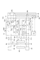
図1は、一実施形態に係るプラズマ処理方法を示す流れ図である。図1に示すプラズマ処理方法MT1は、プラズマ処理装置を用いて実行される。図2は、種々の実施形態に係るプラズマ処理方法において用いることができる一実施形態のプラズマ処理装置を概略的に示す図である。図2には、一実施形態に係るプラズマ処理装置10の縦断面における構造が概略的に示されている。図2に示すプラズマ処理装置10は、容量結合型のプラズマ処理装置である。
FIG. 1 is a flowchart showing a plasma processing method according to an embodiment. The plasma processing method MT1 shown in FIG. 1 is executed using a plasma processing apparatus. FIG. 2 is a diagram schematically showing a plasma processing apparatus of one embodiment that can be used in the plasma processing methods according to various embodiments. FIG. 2 schematically shows a structure in a vertical cross section of the
プラズマ処理装置10は、チャンバ本体12を備えている。チャンバ本体12は、略円筒形状を有している。チャンバ本体12は、その内部空間をチャンバ12cとして提供している。チャンバ本体12は、例えばアルミニウムから構成されている。チャンバ本体12は接地電位に接続されている。チャンバ本体12の内壁面、即ち、チャンバ12cを画成する壁面には、耐プラズマ性を有する膜が形成されている。この膜は、陽極酸化処理によって形成された膜、又は、酸化イットリウムから形成された膜といったセラミック製の膜であり得る。チャンバ本体12の側壁には通路12gが形成されている。基板Wがチャンバ12cに搬入されるとき、また、基板Wがチャンバ12cから搬出されるときに、基板Wは通路12gを通過する。チャンバ本体12の側壁にはゲートバルブ14が取り付けられている。通路12gは、ゲートバルブ14により開閉可能となっている。
The
チャンバ12c内では、支持部15が、チャンバ本体12の底部から上方に延在している。支持部15は、略円筒形状を有しており、石英といった絶縁材料から形成されている。支持部15上にはステージ16が搭載されている。ステージ16は支持部15によって支持されている。
In the
ステージ16は、チャンバ12c内において基板Wを支持するように構成されている。ステージ16は、給電部18及び静電チャック20を含んでいる。給電部18は、後述する高周波電源からの高周波を伝送する伝送路を提供する。静電チャック20は、給電部18上に設けられている。静電チャック20は、基台22及びチャック本体26を含んでいる。基台22は、導電性を有し、下部電極を構成している。基台22は、給電部18上に設けられており、給電部18に電気的に接続されている。
The
基台22内には、流路22fが設けられている。流路22fは、熱交換媒体用の流路である。熱交換媒体は、例えば冷媒である。流路22fには、チャンバ本体12の外部に設けられたチラーユニットTUから熱交換媒体が供給される。流路22fに供給された熱交換媒体は、チラーユニットTUに戻される。このように、流路22fには、当該流路22fとチラーユニットとの間で循環するように、熱交換媒体が供給される。
A
チャック本体26は、基台22上に設けられている。チャック本体26は、基台22に例えば接着剤を介して固定されている。チャック本体26は、基板Wを静電引力により保持するよう構成されている。チャック本体26内には、電極26aが設けられている(図3参照)。電極26aは、膜状の電極である。電極26aには、スイッチSWCを介して直流電源DSCが接続されている。直流電源DSCからの電圧が電極26aに印加されると、チャック本体26上に載置された基板Wとチャック本体26との間で静電引力が発生する。発生した静電引力により、基板Wは、チャック本体26に引き付けられ、当該チャック本体26によって保持される。また、プラズマ処理装置10は、チャック本体26の上面と基板Wの裏面との間に、ガス供給機構からの伝熱ガス、例えばHeガスを供給するガス供給ラインを提供する。
The
チャンバ本体12の底部からは、筒状部28が上方に延在している。筒状部28は、支持部15の外周に沿って延在している。筒状部28は、導電性を有し、略円筒形状を有している。筒状部28は、接地電位に接続されている。支持部15上には、絶縁部29が設けられている。絶縁部29は、絶縁性を有し、石英といったセラミックから形成されている。絶縁部29は、略円筒形状を有しており、給電部18の外周及び静電チャック20の外周に沿って延在している。基台22及びチャック本体26の外周領域上には、フォーカスリングFRが搭載される。フォーカスリングFRは、略環状板形状を有しており、例えばシリコン又は酸化シリコンから形成されている。フォーカスリングFRは、チャック本体26の基板搭載領域のエッジ及び基板Wのエッジを囲むように設けられる。
A
プラズマ処理装置10は、上部電極30を更に備えている。上部電極30は、ステージ16の上方に設けられている。上部電極30は、部材32と共にチャンバ本体12の上部開口を閉じている。部材32は、絶縁性を有している。上部電極30は、この部材32を介してチャンバ本体12の上部に支持されている。
The
上部電極30は、天板34及び支持体36を含んでいる。天板34の下面は、チャンバ12cを画成している。天板34には、複数のガス吐出孔34aが設けられている。複数のガス吐出孔34aの各々は、天板34を板厚方向(鉛直方向)に貫通している。この天板34は、限定されるものではないが、例えばシリコンから形成されている。或いは、天板34は、アルミニウム製の母材の表面に耐プラズマ性の膜を設けた構造を有し得る。この膜は、陽極酸化処理によって形成された膜、又は、酸化イットリウムから形成された膜といったセラミック製の膜であり得る。
The
支持体36は、天板34を着脱自在に支持する部品である。支持体36は、例えばアルミニウムといった導電性材料から形成され得る。支持体36の内部には、ガス拡散室36aが設けられている。ガス拡散室36aからは、複数のガス孔36bが下方に延びている。複数のガス孔36bは、複数のガス吐出孔34aにそれぞれ連通している。支持体36には、ガス拡散室36aにガスを導くガス導入口36cが形成されており、このガス導入口36cには、ガス供給管38が接続されている。
The
ガス供給管38には、バルブ群42及び流量制御器群44を介して、ガスソース群40が接続されている。ガスソース群40は、複数のガスソースを含んでいる。バルブ群42は複数のバルブを含んでおり、流量制御器群44は複数の流量制御器を含んでいる。流量制御器群44の複数の流量制御器の各々は、マスフローコントローラ又は圧力制御式の流量制御器である。ガスソース群40の複数のガスソースはそれぞれ、バルブ群42の対応のバルブ及び流量制御器群44の対応の流量制御器を介して、ガス供給管38に接続されている。プラズマ処理装置10は、ガスソース群40の複数のガスソースのうち選択された一以上のガスソースからのガスを、個別に調整された流量で、チャンバ12cに供給することが可能である。
A
筒状部28とチャンバ本体12の側壁との間には、バッフルプレート48が設けられている。バッフルプレート48は、例えば、アルミニウム製の母材に酸化イットリウム等のセラミックを被覆することにより構成され得る。このバッフルプレート48には、多数の貫通孔が形成されている。バッフルプレート48の下方においては、排気管52がチャンバ本体12の底部に接続されている。この排気管52には、排気装置50が接続されている。排気装置50は、自動圧力制御弁といった圧力制御器、及び、ターボ分子ポンプといった真空ポンプを有しており、チャンバ12cを減圧することができる。
A
プラズマ処理装置10は、第1の高周波電源62を更に備えている。第1の高周波電源62は、プラズマ生成用の第1の高周波を発生する電源である。第1の高周波は、27〜100MHzの範囲内の周波数、例えば60MHzの周波数を有する。第1の高周波電源62は、整合器63を介して上部電極30に接続されている。整合器63は、第1の高周波電源62の出力インピーダンスと負荷側(上部電極30側)のインピーダンスを整合させるための回路を有している。なお、第1の高周波電源62は、整合器63を介して給電部18に接続されていてもよい。第1の高周波電源62が給電部18に接続されている場合には、上部電極30は接地電位に接続される。
The
プラズマ処理装置10は、第2の高周波電源64を更に備えている。第2の高周波電源64は、基板Wにイオンを引き込むためのバイアス用の第2の高周波を発生する電源である。第2の高周波の周波数は、第1の高周波の周波数よりも低い。第2の高周波の周波数は、400kHz〜13.56MHzの範囲内の周波数であり、例えば、400kHzである。第2の高周波電源64は、整合器65及び給電体66を介して給電部18に接続されている。整合器65は、第2の高周波電源64の出力インピーダンスと負荷側(給電部18側)のインピーダンスを整合させるための回路を有している。
The
一実施形態においては、プラズマ処理装置10は、主制御部MCを更に備え得る。主制御部MCは、プロセッサ、記憶装置、入力装置、表示装置等を備えるコンピュータであり、プラズマ処理装置10の各部を制御する。具体的に、主制御部MCは、記憶装置に記憶されている制御プログラムを実行し、当該記憶装置に記憶されているレシピデータに基づいてプラズマ処理装置10の各部を制御する。これにより、プラズマ処理装置10は、レシピデータによって指定されたプロセスを実行するようになっている。
In one embodiment, the
以下、ステージ16について詳細に説明する。図3は、一実施形態に係るステージの断面図である。図4は、一実施形態に係るステージを、プラズマ処理装置の他の構成部品と共に概略的に示す図である。図3及び図4に示すように、ステージ16は、給電部18及び静電チャック20を有している。
Hereinafter, the
給電部18は、上述したように、高周波電源(例えば、第2の高周波電源64)からの高周波の伝送路を提供する。給電部18は、導電性を有しており、例えば金属から形成されている。給電部18には、上述の給電体66が接続されている。給電部18は、一実施形態では、その内部空間を収容空間18sとして提供している。
The
一実施形態において、給電部18は、第1の部材18a、第2の部材18b、及び、第3の部材18cを有している。第1の部材18a、第2の部材18b、及び、第3の部材18cは、導電性を有しており、例えば、金属から形成されている。第1の部材18aは、平面視では略円形の部材であり、その中央部分において下方に突出している。第1の部材18aの中央部分には、給電体66が接続されている。第2の部材18bは、第1の部材18a上に搭載されており、当該第1の部材18aに接続されている。第2の部材18bは、略リング形状を有している。第3の部材18cは、第2の部材18b上に搭載されており、第2の部材18bに接続されている。第3の部材18cは、略円盤形状を有している。第1の部材18a、第2の部材18b、及び、第3の部材18cは、高周波の伝送路を構成している。第1の部材18a、第2の部材18b、及び、第3の部材18cから構成された組立体は、収容空間18sを画成している。
In one embodiment, the
静電チャック20は、給電部18上に設けられている。静電チャック20は、上述したように、基台22及びチャック本体26を有している。基台22は、略円盤形状を有している。上述したように、基台22内には熱交換媒体用の流路22fが形成されている。基台22は、導電性を有しており、アルミニウムといった金属から形成されている。基台22は、給電部18上に設けられており、給電部18に電気的に接続されている。基台22は、プラズマ処理装置10の下部電極を構成している。
The
チャック本体26は、基台22上に設けられている。チャック本体26は、基台22の上面に、例えば接着剤を介して、固定されている。チャック本体26は、セラミック本体260を有している。セラミック本体260は、セラミックから形成されており、略円盤形状を有している。
The
セラミック本体260は、基板搭載領域260a及び外周領域260bを有している。基板搭載領域260aは、略円盤形状の領域である。基板搭載領域260aの上面は、その上に基板Wが載置されるチャック本体26の上面である。外周領域260bは、略環状板形状の領域であり、基板搭載領域260aを囲むように延在している。即ち、外周領域260bは、基板搭載領域260aの外側で、チャック本体26及びセラミック本体260の中心軸線AXに対して周方向に延在している。基板搭載領域260a及び外周領域260bは、チャック本体26の連続する平坦な下面(裏面)を提供している。外周領域260bの上面は、基板搭載領域260aの上面よりも、チャック本体26の裏面の近くにおいて延在している。外周領域260b上には図2に示すようにフォーカスリングFRが搭載される。
The
チャック本体26は、電極26a、複数の第1のヒータ26b、及び、複数の第2のヒータ26cを有している。電極26aは、基板搭載領域260a内において中心軸線AXに直交する方向に延在している。複数の第1のヒータ26b及び複数の第2のヒータ26cの各々は、薄膜抵抗ヒータである。複数の第1のヒータ26b及び複数の第2のヒータ26cは、セラミック本体260内に設けられている。複数の第1のヒータ26b及び複数の第2のヒータ26cは、電極26aとチャック本体26の裏面との間に設けられている。複数の第1のヒータ26bは、中心軸線AXに直交するチャック本体26内の面上で分布されている。複数の第2のヒータ26cの個数は、複数の第1のヒータ26bの個数よりも多い。複数の第2のヒータ26cは、中心軸線AXに直交するチャック本体26内の別の面上で分布されている。
The
図5は、図3に示すステージの複数の第1のヒータのレイアウトの例を示す平面図である。図5は、中心軸線AXに直交する面内での複数の第1のヒータ26bのレイアウトを例示している。図5に示すように、一実施形態において、複数の第1のヒータ26bは、中心軸線AXに対して同軸に設けられている。具体的に、複数の第1のヒータ26bのうち中央に設けられている第1のヒータ26bの平面形状は円形である。他の第1のヒータ26bは、中央に設けられている第1のヒータ26bを囲む環形状を有している。即ち、中央に設けられている第1のヒータ26b以外の第1のヒータ26bは、周方向に延在する帯状をなしている。一実施形態において、複数の第1のヒータ26bのうち一部のヒータは少なくとも外周領域260b内に設けられている。例えば、複数の第1のヒータ26bのうち中心軸線AXに対して最も外側で延在する第1のヒータ26bは、外周領域260b内に設けられており、他の第1のヒータ26bは、基板搭載領域260a内に設けられている。複数の第1のヒータ26bは、当該複数の第1のヒータ26bがそれぞれ配置されている複数のゾーンZ1を加熱する。
FIG. 5 is a plan view showing a layout example of the plurality of first heaters of the stage shown in FIG. FIG. 5 illustrates the layout of the plurality of
なお、複数の第1のヒータ26bは、更に中心軸線AXに対して周方向に沿って配列されていてもよい。即ち、複数のゾーンZ1は、中心のゾーン、及び、当該中心のゾーンの外側の同軸の複数の領域内において周方向に並ぶ複数のゾーンを含んでいてもよく、これら複数のゾーンZ1内に複数の第1のヒータ26bがそれぞれ設けられていてもよい。
The plurality of
図6は、図3に示すステージの複数の第2のヒータのレイアウトの例を示す平面図である。図6は、中心軸線AXに直交する面内での複数の第2のヒータ26cのレイアウトを例示している。複数の第2のヒータ26cは、基板搭載領域260a内で分布するように設けられている。図6に示すように、一例においては、複数の第2のヒータ26cは、複数のゾーンZ2内にそれぞれ設けられている。複数のゾーンZ2は、中心軸線AXに交差する中心のゾーン、及び、中心軸線AXに対して同軸の複数の領域内で周方向に並ぶ複数のゾーンを含む。なお、複数のゾーンZ2の各々、即ち、複数の第2のヒータ26cは、複数のゾーンZ1の何れかの中に内包される。
FIG. 6 is a plan view showing an example of the layout of the plurality of second heaters of the stage shown in FIG. FIG. 6 illustrates the layout of the plurality of
図3及び図4に示すように、複数の第2のヒータ26cは、チャック本体26の上面(即ち、基板搭載領域260aの上面)と複数の第1のヒータ26bとの間に設けられている。即ち、複数の第2のヒータ26cは、複数の第1のヒータ26bに対して上側に設けられている。なお、複数の第2のヒータ26cは、複数の第1のヒータ26bに対して下側に設けられていてもよい。
As shown in FIGS. 3 and 4, the plurality of
複数の第1のヒータ26bは、第1の電源80からの出力によって駆動されることにより発熱する。第1の電源80の出力は、交流又は直流の出力である。即ち、第1の電源80の出力は、交流出力及び直流出力の何れであってもよい。複数の第2のヒータ26cは、第2の電源82からの出力によって駆動されることにより発熱する。第2の電源82の出力は、交流又は直流の出力である。即ち、第2の電源82の出力は、交流出力及び直流出力の何れであってもよい。一実施形態では、複数の第1のヒータ26bは、第1の電源からの交流出力により交流駆動され、複数の第2のヒータ26cは、第2の電源からの直流出力により直流駆動される。複数の第1のヒータ26b及び複数の第2のヒータ26cの駆動のために、ステージ16は、第1のヒータコントローラ71及び第2のヒータコントローラ72を有している。以下、図3及び図4と共に、図7及び図8を参照する。図7は、図3に示すステージのチャック本体の裏面における端子のレイアウトの例を示す平面図である。図8は、図3に示すステージの制御に関連する一実施形態の構成を示す図である。
The plurality of
複数の第1のヒータ26bのそれぞれには、複数の第1の給電線73が電気的に接続されている。複数の第1のヒータ26bの各々には、一対の第1の給電線73が接続されている。複数の第2のヒータ26cのそれぞれには、複数の第2の給電線74が電気的に接続されている。複数の第2のヒータ26cの各々には、一対の第2の給電線74が接続されている。一実施形態において、複数の第2の給電線74は、複数のフレキシブルプリント回路基板によって提供され得る。複数のフレキシブルプリント回路基板の各々は、複数の第2の給電線74のうち対応の幾つかの第2の給電線74を提供している。一実施形態において、第1のヒータコントローラ71、複数の第1の給電線73、第2のヒータコントローラ72、及び、複数の第2の給電線74は、収容空間18s内に設けられている。
A plurality of first
図7に示すように、チャック本体26の裏面には、複数の端子26e及び複数の端子26fが設けられている。複数の端子26eには、複数の第1の給電線73がそれぞれ接続されている。複数の端子26eは、チャック本体26内の内部配線を介して、複数の第1のヒータ26bに接続されている。複数の端子26fには、複数の第2の給電線74が接続されている。複数の第2の給電線74が複数のフレキシブルプリント回路基板によって提供されている場合には、複数の端子26fは、複数の端子群にグループ化されている。複数の端子26fは、チャック本体26内の内部配線を介して、複数の第2のヒータ26cに接続されている。一実施形態において、複数の端子26e及び複数の端子26fは、外周領域260b内に設けられている。一実施形態において、複数の端子26e及び複数の端子26f(又は複数の端子群)は、外周領域260bの全周にわたって周方向に分散されている。
As shown in FIG. 7, a plurality of
複数の第1の給電線73は、第1のヒータコントローラ71に接続されている。第1のヒータコントローラ71は、第1の電源80に接続されている。第1のヒータコントローラ71は、第1の電源80からの出力により複数の第1のヒータ26bを駆動するよう構成されている。一実施形態では、第1のヒータコントローラ71は、第1の電源80からの出力を分配することにより生成した複数の第1の出力により複数の第1のヒータ26bをそれぞれ駆動するように構成されている。複数の第1のヒータ26bを駆動するために、第1のヒータコントローラ71は、複数の第1の給電線73を介して、複数の第1のヒータ26bに複数の第1の出力をそれぞれ供給する。第1のヒータコントローラ71は、複数の第1のヒータ26bにそれぞれ供給される複数の第1の出力の電力量を個別に調整するように構成されている。一実施形態では、第1の電源80からの出力は交流出力であり、第1のヒータコントローラ71は、各々が交流出力である複数の第1の出力により、複数の第1のヒータ26bを交流駆動するよう構成されている。
The plurality of first
複数の第2の給電線74は、第2のヒータコントローラ72に接続されている。第2のヒータコントローラ72は、第2の電源82に接続されている。第2のヒータコントローラ72は、第2の電源82からの出力により複数の第2のヒータ26cを駆動するよう構成されている。一実施形態では、第2のヒータコントローラ72は、第2の電源82からの出力を分配することにより生成した複数の第2の出力により複数の第2のヒータ26cをそれぞれ駆動するように構成されている。複数の第2のヒータ26cを駆動する電力は複数の第1のヒータ26bを駆動する電力よりも低い。複数の第2のヒータ26cを駆動するために、第2のヒータコントローラ72は、複数の第2の給電線74を介して、複数の第2のヒータ26cに複数の第2の出力をそれぞれ供給する。第2のヒータコントローラ72は、複数の第2のヒータ26cにそれぞれ供給される複数の第2の出力の電力量を個別に調整するように構成されている。
The plurality of second
一実施形態では、第2の電源82からの出力は直流出力であり、第2のヒータコントローラ72は、各々が直流出力である複数の第2の出力により、複数の第2のヒータ26cを直流駆動するよう構成されている。第1の電源80が交流電源であり、第2の電源82が直流電源である場合には、第2の電源82は、図示されるように、第1の電源80に接続される。この場合に、第2の電源82は、第1の電源80からの交流出力を直流に変換するAC/DCコンバータであり、例えば、スイッチング電源である。
In one embodiment, the output from the
図8に示すように、第1のヒータコントローラ71内には、複数の配線71f及び複数の配線71rが設けられている。複数の配線71fの各々の一端は、複数の第1の給電線73のうち対応の第1の給電線73を介して、複数の第1のヒータ26bのうち対応の第1のヒータ26bに接続されている。複数の配線71rの各々の一端は、複数の第1の給電線73のうち対応の第1の給電線73を介して、複数の第1のヒータ26bのうち対応の第1のヒータ26bに接続されている。
As shown in FIG. 8, a plurality of
複数の配線71fの各々の他端は、フィルタF11(第1のフィルタ)を介して第1の電源80に接続されている。具体的には、複数の配線71fの他端は、図3に示す端子ET11に接続しており、当該端子ET11は、フィルタユニットFUの端子FT11に接続している。フィルタユニットFUは、フィルタF11、フィルタF12(第1のフィルタ)、フィルタF21(第2のフィルタ)、及び、フィルタF22(第2のフィルタ)を有している。フィルタF11、フィルタF12、フィルタF21、及び、フィルタF22を含むフィルタユニットFUは、上述した収容空間18sに対して給電部18の外側に設けられている。
The other end of each of the plurality of
端子FT11は、フィルタF11に接続されている。フィルタF11は、第1の電源80への高周波の流入を抑制する。フィルタF11は、例えばLCフィルタである。フィルタF11のコイルの一端には、端子FT11が接続されている。フィルタF11のコイルは、第1の電源80と第1のヒータコントローラ71との間の給電線を部分的に構成している。フィルタF11のコイルの他端は、当該フィルタF11のコンデンサを介してグランドに接続されている。
The terminal FT11 is connected to the filter F11. The filter F11 suppresses the inflow of high frequency waves into the
複数の配線71rの各々の他端は、フィルタF12を介して第1の電源80に接続されている。具体的には、複数の配線71rの他端は、図3に示す端子ET12に接続しており、当該端子ET12は、フィルタユニットFUの端子FT12に接続している。端子FT12は、フィルタF12に接続されている。フィルタF12は、第1の電源80への高周波の流入を抑制する。フィルタF12は、例えばLCフィルタである。フィルタF12のコイルの一端には、端子FT12が接続されている。フィルタF12のコイルは、第1の電源80と第1のヒータコントローラ71との間の配線を部分的に構成している。フィルタF12のコイルの他端は、当該フィルタF12のコンデンサを介してグランドに接続されている。
The other end of each of the plurality of
なお、図10を参照して後述する実施形態では、第1の電源80と第1のヒータコントローラ71との間の給電線及び配線上には、スイッチング部84が設けられている。具体的に、スイッチング部84は、フィルタF11と第1の電源80との間、及び、フィルタF12と第1の電源80との間に設けられている。スイッチング部84は、第1の電源80と第1のヒータコントローラ71との間の接続を遮断可能に構成されている。
In the embodiment described later with reference to FIG. 10, the switching
図8に示すように、第2のヒータコントローラ72内には、複数の配線72p及び複数の配線72gが設けられている。複数の配線72pの各々の一端は、複数の第2の給電線74のうち対応の第2の給電線74を介して、複数の第2のヒータ26cのうち対応の第2のヒータ26cに接続されている。複数の配線72gの各々の一端は、複数の第2の給電線74のうち対応の第2の給電線74を介して、複数の第2のヒータ26cのうち対応の第2のヒータ26cに接続されている。
As shown in FIG. 8, a plurality of
複数の配線72pの各々の他端は、フィルタF21を介して第2の電源82に接続されている。具体的には、複数の配線72pの他端は、図3に示す端子ET21に接続しており、当該端子ET21は、フィルタユニットFUの端子FT21に接続している。端子FT21は、フィルタF21に接続されている。フィルタF21は、第2の電源82への高周波の流入を抑制する。フィルタF21は、例えばLCフィルタである。フィルタF21のコイルの一端には、端子FT21が接続されている。フィルタF21のコイルは、第2の電源82と第2のヒータコントローラ72との間の給電線を部分的に構成している。フィルタF21のコイルの他端は、当該フィルタF21のコンデンサを介してグランドに接続されている。
The other end of each of the plurality of
複数の配線72gの各々の他端は、フィルタF22を介して第2の電源82に接続されている。具体的には、複数の配線72gの他端は、別の端子に接続しており、当該別の端子は、フィルタユニットFUの別の端子に接続している。フィルタユニットFUの当該別の端子は、フィルタF22に接続されている。フィルタF22は、第2の電源82への高周波の流入を抑制するためのフィルタである。フィルタF22は、例えばLCフィルタである。フィルタF22のコイルの一端には、フィルタユニットFUの当該別の端子が接続されている。フィルタF22のコイルは、第2の電源82のグランドと第2のヒータコントローラ72との間の配線を部分的に構成している。フィルタF22のコイルの他端は、当該フィルタF22のコンデンサを介してグランドに接続されている。
The other end of each of the plurality of wires 72g is connected to the
第2の電源82と第2のヒータコントローラ72との間の給電線及び配線上には、スイッチング部86が設けられている。具体的に、スイッチング部86は、フィルタF21と第2の電源82との間、及び、フィルタF22と第2の電源82との間に設けられている。スイッチング部86は、第2の電源82と第2のヒータコントローラ72との間の接続を遮断可能に構成されている。
A switching
図8に示すように、第1のヒータコントローラ71は、制御回路71c及び複数のスイッチング素子SWAを有している。複数のスイッチング素子SWAは、複数の配線71f上にそれぞれ設けられている。複数のスイッチング素子SWAの各々は、半導体スイッチング素子であることができ、例えばトライアックであり得る。第1のヒータコントローラ71は、第1の電源80からの出力(例えばAC200Vの交流出力)を受けて、複数の第1のヒータ26bのそれぞれに対する複数の第1の出力(例えばAC200Vの交流出力)を生成する。第1のヒータコントローラ71では、複数のスイッチング素子SWAの状態が導通状態と遮断状態の間で切り替えられることにより、複数の第1のヒータ26bのそれぞれに対する複数の第1の出力の供給と供給停止とが切り替えられる。複数のスイッチング素子SWAの状態は、制御回路71cにより設定される。
As shown in FIG. 8, the
第1の電源80が交流電源である実施形態において、第1のヒータコントローラ71は、AC/DCコンバータ71a、及び、DC/DCコンバータ71dを更に有している。AC/DCコンバータ71aは、第1の電源80の交流出力から直流出力(例えばDC15Vの直流出力)を生成する。DC/DCコンバータ71dは、AC/DCコンバータ71aによって生成される直流出力から、別の直流出力(例えばDC3.3Vの直流出力)を生成する。DC/DCコンバータ71dによって生成された直流出力は、制御回路71cといった第1のヒータコントローラ71内のデバイスの動作電源として利用される。
In the embodiment in which the
図4及び図8に示すように、ステージ16には、複数の温度センサTSが設けられている。複数の温度センサTSは、チャック本体26の複数のゾーンZ1のそれぞれの温度を測定するよう、ステージ16に取り付けられている。例えば、複数の温度センサTSは、複数のゾーンZ1のそれぞれの温度をチャック本体26の裏面から測定する。複数の温度センサTSの各々は、例えば蛍光式温度センサである。複数の温度センサTSはセンサ回路TCに接続されている。複数の温度センサTSそれぞれの出力は、センサ回路TCにおいてデジタルの電気信号、即ち、複数のゾーンZ1のそれぞれの温度の測定値に変換される。複数のゾーンZ1のそれぞれの温度の測定値は、上位コントローラUCに与えられる。
As shown in FIGS. 4 and 8, the
第2のヒータコントローラ72は、内部コントローラ72f、制御回路72c、及び、複数のスイッチング素子SWDを有している。複数のスイッチング素子SWDは、複数の配線72p上にそれぞれ設けられている。複数のスイッチング素子SWDの各々は、半導体スイッチング素子であることができ、例えばフォトMOSリレーであり得る。第2のヒータコントローラ72は、第2の電源82からの出力(例えば、DC15Vの直流出力)を受けて、複数の第2のヒータ26cのそれぞれに対する複数の第2の出力を生成する。第2のヒータコントローラ72では、複数のスイッチング素子SWDの状態が導通状態と遮断状態の間で切り替えられることにより、複数の第2のヒータ26cのそれぞれに対する複数の第2の出力の供給と供給停止とが切り替えられる。複数のスイッチング素子SWDの状態は、制御回路72cにより設定される。
The
第2のヒータコントローラ72は、DC/DCコンバータ72dを更に有している。DC/DCコンバータ72dは、AC/DCコンバータ71aによって生成される直流出力から、別の直流出力(例えばDC3.3Vの直流出力)を生成する。DC/DCコンバータ72dによって生成された直流出力は、内部コントローラ72f及び制御回路72cといった第2のヒータコントローラ72内のデバイスの動作電源として利用される。
The
複数の配線72p上には、複数の抵抗素子72rがそれぞれ設けられている。第2のヒータコントローラ72は、複数の測定器72mを更に有している。複数の測定器72mは、複数の抵抗素子72rの両端間の電圧をそれぞれ測定し、複数の配線72pを流れる電流をそれぞれ測定する。複数の測定器72mによって取得された電圧の測定値及び電流の測定値は、内部コントローラ72f、及び、光ブリッジOBを介して上位コントローラUCに与えられる。
A plurality of
第2のヒータコントローラ72の内部コントローラ72fは、光ブリッジOBを介して上位コントローラUCに接続されている。内部コントローラ72fは、例えばFPGA(field−programmable gate array)から構成され得る。内部コントローラ72fは、光ブリッジOBを介して上位コントローラUCと通信し、制御回路71c及び制御回路72cを制御する。上位コントローラUCは、CPUといったプロセッサ、及び、メモリといった記憶装置を備えるマイクロコンピュータから構成され得る。プラズマ処理装置10では、主制御部MCから上位コントローラUCに基板Wの面内温度分布の設定データが与えられる。
The
上位コントローラUCは、基板Wの面内温度分布の設定データから、複数のゾーンZ1それぞれの目標温度、及び、複数の第2の出力それぞれの所定時間当りの電力量の目標値を決定する。上位コントローラUCは、複数のゾーンZ1それぞれの目標温度に応じた電力量(所定時間当りの電力量)の複数の第1の出力が複数の第1のヒータ26bに供給されるよう、光ブリッジOBを介して内部コントローラ72fに制御信号を送出する。内部コントローラ72fは、上位コントローラUCからの制御信号に応答して、制御回路71cを制御することにより、複数の第1のヒータ26bにそれぞれ供給される複数の第1の出力の電力量を制御する。
The upper controller UC determines the target temperature of each of the plurality of zones Z1 and the target value of the power amount per predetermined time of each of the plurality of second outputs from the setting data of the in-plane temperature distribution of the substrate W. The host controller UC uses the optical bridge OB so that the plurality of first outputs having the power amounts (power amounts per predetermined time) according to the target temperatures of the plurality of zones Z1 are supplied to the plurality of
上位コントローラUCは、複数の温度センサTS及びセンサ回路TCによって取得される複数のゾーンZ1のそれぞれの温度の測定値と複数のゾーンZ1のそれぞれの目標温度との間の誤差を減少させるよう、複数の第1のヒータ26bにそれぞれ供給される複数の第1の出力の電力量のフィードバック制御を実行する。複数の第1のヒータ26bにそれぞれ供給される複数の第1の出力の電力量のフィードバック制御は、例えばPID制御である。なお、上位コントローラUCは、複数の第1のヒータ26bにそれぞれ供給される複数の第1の出力の電力量のフィードバック制御において、複数のゾーンZ1のそれぞれの温度の測定値の時系列から求められる複数のゾーンZ1のそれぞれの温度の移動平均値と複数のゾーンZ1のそれぞれの目標温度との間の誤差を求めてもよい。
The upper controller UC is configured to reduce the error between the measured value of each temperature of the plurality of zones Z1 acquired by the plurality of temperature sensors TS and the sensor circuit TC and the target temperature of each of the plurality of zones Z1. The feedback control of the electric energy of the plurality of first outputs respectively supplied to the
一実施形態では、第1のヒータコントローラ71の複数の第1の出力の電力は実質的に同一であり且つ一定である。この実施形態において、第1のヒータコントローラ71は、複数の第1のデューティー比を制御するように構成されている。複数の第1のデューティー比は、複数の第1の出力がそれぞれ複数の第1のヒータ26bに供給される供給時間長の所定時間長(例えば100ミリ秒)中の比率である。上位コントローラUCは、複数の第1のデューティー比を、光ブリッジOBを介して、内部コントローラ72fに指定する。内部コントローラ72fは、制御回路71cを制御することにより、指定された複数の第1のデューティー比に応じて、所定時間内での複数のスイッチング素子SWAそれぞれの状態(導通状態と遮断状態)を切り替える。これにより、複数の第1のヒータ26bのそれぞれに対する複数の第1の出力の供給と供給停止とが交互に切り替えられる。
In one embodiment, the power of the plurality of first outputs of the
上位コントローラUCは、複数の温度センサTS及びセンサ回路TCによって取得される複数のゾーンZ1のそれぞれの温度の測定値と複数のゾーンZ1のそれぞれの目標温度との間の誤差を減少させるよう、複数の第1のデューティー比を調整する。即ち、上位コントローラUCは、複数の第1のデューティー比のフィードバック制御を実行する。複数の第1のデューティー比のフィードバック制御は、例えばPID制御である。なお、上位コントローラUCは、複数の第1のデューティー比のフィードバック制御において、複数のゾーンZ1のそれぞれの温度の測定値の時系列から求められる複数のゾーンZ1のそれぞれの温度の移動平均値と複数のゾーンZ1のそれぞれの目標温度との間の誤差を求めてもよい。 The upper controller UC is configured to reduce the error between the measured value of each temperature of the plurality of zones Z1 acquired by the plurality of temperature sensors TS and the sensor circuit TC and the target temperature of each of the plurality of zones Z1. The first duty ratio of is adjusted. That is, the host controller UC executes feedback control of the plurality of first duty ratios. The feedback control of the plurality of first duty ratios is, for example, PID control. In the feedback control of the plurality of first duty ratios, the host controller UC uses a moving average value of each temperature of the plurality of zones Z1 and a plurality of moving average values of the temperature of each of the plurality of zones Z1 obtained from the time series of the measured values of the respective temperatures of the plurality of zones Z1. The error between each of the target temperatures of the zone Z1 may be obtained.
上位コントローラUCは、基板Wの面内温度分布の設定データに基づいて決定した所定時間当りの電力量の目標値に応じた複数の第2の出力が複数の第2のヒータ26cにそれぞれ供給されるよう、光ブリッジOBを介して内部コントローラ72fに制御信号を送出する。内部コントローラ72fは、上位コントローラUCからの制御信号に応答して、制御回路72cを制御することにより、複数の第2のヒータ26cにそれぞれ供給される複数の第2の出力の電力量(所定時間当りの電力量)を制御する。
The host controller UC supplies a plurality of second outputs to the plurality of
上位コントローラUCは、複数の電力の測定値に基づいて、複数の第2の出力の電力量のフィードバック制御を実行する。複数の第2の出力の電力量のフィードバック制御は、例えばPID制御である。複数の電力の測定値の各々は、複数の測定器72mのうち対応の測定器72mによって取得された電圧の測定値と電流の測定器の積である。なお、複数の第2の出力の各々が交流出力である場合には、複数の電力の測定値の各々は、複数の測定器72mのうち対応の測定器72mによって取得された電圧の測定値と電流の測定器の積から求められる実効値であり得る。別の実施形態において、複数の第2の出力の電力量の各々は、複数の測定器72mのうち対応の測定器72mによって取得された電圧の測定値と電流の測定器の積の時系列の移動平均値に基づいて制御されてもよい。なお、複数の第2の出力の各々が交流出力である場合には、複数の電力の測定値の各々は、複数の測定器72mのうち対応の測定器72mによって取得された電圧の測定値と電流の測定器の積から求められる実効値の時系列の移動平均値であり得る。
The upper controller UC executes feedback control of the power amounts of the plurality of second outputs based on the measured values of the plurality of powers. The feedback control of the power amounts of the plurality of second outputs is, for example, PID control. Each of the plurality of measured values of electric power is the product of the measured value of voltage and the measured value of current obtained by the
一実施形態では、第2のヒータコントローラ72の複数の第2の出力の電力は実質的に同一且つ一定である。この実施形態において、第2のヒータコントローラ72は、複数の第2のデューティー比を制御するように構成されている。複数の第2のデューティー比は、複数の第2の出力がそれぞれ複数の第2のヒータ26cに供給される供給時間長の所定時間長(例えば100ミリ秒)中の比率である。上位コントローラUCは、複数の第2のデューティー比を、光ブリッジOBを介して、内部コントローラ72fに指定する。内部コントローラ72fは、制御回路72cを制御することにより、指定された複数の第2のデューティー比に応じて、所定時間内での複数のスイッチング素子SWDそれぞれの状態(導通状態と遮断状態)を切り替える。これにより、複数の第2のヒータ26cのそれぞれに対する複数の第2の出力の供給と供給停止とが交互に切り替えられる。
In one embodiment, the power of the second outputs of the
上位コントローラUCは、複数の第2の出力の各々の電力の測定値と複数の第2のデューティー比のうち対応の第2のデューティー比との積と電力量の目標値との間の誤差を減少させるように、複数の第2のデューティー比を調整する。即ち、上位コントローラUCは、複数の第2のデューティー比のフィードバック制御を実行する。複数の第2のデューティー比のフィードバック制御は、例えばPID制御である。なお、上位コントローラは、複数の第2のデューティー比のフィードバック制御において、複数の第2の出力の各々の電力の測定値と対応の第2のデューティー比との積の時系列の移動平均値と目標値との誤差を求めてもよい。 The host controller UC determines the error between the product of the measured value of each of the plurality of second outputs and the corresponding second duty ratio among the plurality of second duty ratios and the target value of the electric energy. The plurality of second duty ratios are adjusted so as to decrease. That is, the upper controller UC executes feedback control of the plurality of second duty ratios. The feedback control of the plurality of second duty ratios is, for example, PID control. Note that, in the feedback control of the plurality of second duty ratios, the host controller sets the time-series moving average value of the product of the measured value of the power of each of the plurality of second outputs and the corresponding second duty ratio. An error from the target value may be obtained.
上述したように、上位コントローラUCは、基板Wの面内温度分布の設定データから、複数の第2の出力それぞれの所定時間当りの電力量の目標値を決定する。具体的に、上位コントローラUCは、基板Wの面内温度分布の設定データから、複数の第2のヒータ26cそれぞれによる目標温度上昇量を決定し、当該目標温度上昇量から、複数の第2のヒータ26cそれぞれに供給される第2の出力の所定時間当りの電力量の目標値を決定する。このために、上位コントローラUCは、複数の第2のヒータ26cそれぞれによる温度上昇量を、複数の第2のヒータ26cそれぞれに供給される第2の出力の所定時間当りの電力量に変換する関数を予め保持している。以下、図9を参照し、複数の第2のヒータ26cそれぞれによる温度上昇量を、複数の第2のヒータ26cそれぞれに供給される第2の出力の所定時間当りの電力量に変換する関数を求める手法について説明する。
As described above, the upper controller UC determines the target value of the amount of power per predetermined time of each of the plurality of second outputs from the setting data of the in-plane temperature distribution of the substrate W. Specifically, the host controller UC determines the target temperature increase amount by each of the plurality of
この関数を求める際には、複数の第2のヒータ26cのうち、それらの下方に温度センサTS(以下、「特定の温度センサTS」という)が配置されている特定の第2のヒータ26cに第2の出力が与えられる。なお、特定の第2のヒータ26cの個数は、図9に示す例では三つである。そして、当該特定の第2のヒータ26cの上方のチャック本体26の上面内の特定の領域の赤外線エネルギーが、赤外線カメラIRCによって取得される。なお、当該特定の領域の個数は、特定の第2のヒータ26cの個数と同数である。赤外線カメラIRCによって取得された特定の領域の赤外線エネルギーの測定値は、コンピュータPCに入力される。コンピュータPCには、特定の温度センサTSからの温度の測定値も入力される。そして、コンピュータPCにおいて、特定の温度センサTSからの温度の測定値と赤外線カメラIRCからの特定の領域の赤外線エネルギーの測定値から、赤外線エネルギーの測定値を温度に変換する変換係数が作成される。
When obtaining this function, among the plurality of
変換係数が作成された後、特定の第2のヒータ26cに第2の出力が与えられる。そして、特定の領域の赤外線エネルギーが赤外線カメラIRCによって測定される。赤外線カメラIRCによって取得された特定の領域の赤外線エネルギーの測定値は、コンピュータPCに入力される。そして、コンピュータPCにおいて、変換係数を用いて、特定の領域の赤外線エネルギーの測定値から当該特定の領域の温度が計算される。かかる処理が、上述した第2のデューティー比を変更することによって第2の出力の所定時間当りの電力量を変更しつつ、繰り返される。そして、計算された特定の領域の温度から得られる温度上昇量と、与えられた第2の出力の所定時間当りの電力量との関係から、特定の第2のヒータ26cの各々に関して、温度上昇量を第2の出力の所定時間当りの電力量に変換する関数が求められる。
After the conversion coefficient is created, the second output is given to the specific
上位コントローラUCは、目標温度上昇量に対応する第2の出力の所定時間当りの電力量を、求められた対応の関数を用いて特定することにより、複数の第2のヒータ26cそれぞれに供給される第2の出力の所定時間当りの電力量の目標値を決定する。なお、特定の第2のヒータ26cのうち任意の一つの第2のヒータ26cと同一のゾーンZ1に内包される他の第2のヒータ26cに供給される第2の出力の所定時間当りの電力量の目標値を決定する際には、当該任意の一つの第2のヒータ26cを用いて求められた関数が用いられる。
The upper controller UC supplies each of the plurality of
図4及び図8を再び参照する。上述したように、第2の電源82と第2のヒータコントローラ72との間の給電線上には、スイッチング部86が設けられている。スイッチング部86は、第2の電源82と第2のヒータコントローラ72との間の接続を遮断可能に構成されている。スイッチング部86は、例えばマグネティックコンタクタから構成されている。スイッチング部86は、制御部CBに接続されている。制御部CBは、第2のヒータコントローラ72と第2の電源82との間の接続状態を設定するよう、スイッチング部86を制御する。
Please refer to FIG. 4 and FIG. 8 again. As described above, the switching
主制御部MCは、複数の第2のヒータ26cを駆動する場合には、制御部CBに制御信号を送出して、スイッチング部86に第2のヒータコントローラ72と第2の電源82とを互いに接続させる。一方、主制御部MCは、複数の第2のヒータ26cを利用しない場合、即ち、複数の第2のヒータ26cの駆動を停止する場合には、制御部CBに制御信号を送出して、スイッチング部86に第2のヒータコントローラ72と第2の電源82との間の接続を遮断させる。主制御部MCは、第2のヒータコントローラ72と第2の電源82との間の接続を遮断する場合には、第2のヒータコントローラ72と第2の電源82との間の接続が遮断されていることを伝達する信号を上位コントローラUCに送出する。これにより、第2のヒータコントローラ72から上位コントローラUCに送信される信号によって上位コントローラUCが誤動作することが防止される。
When driving the plurality of
以下、図10を参照する。図10は、図3に示すステージの制御に関連する別の実施形態の構成を示す図である。図10に示す実施形態は、第1の電源80と第1のヒータコントローラ71との間の給電線上にスイッチング部84が設けられている点で、図8に示した実施形態と異なっている。スイッチング部84は、第1の電源80と第1のヒータコントローラ71との間の接続を遮断可能に構成されている。スイッチング部84は、例えばマグネティックコンタクタから構成されている。スイッチング部84は、制御部CBに接続されている。制御部CBは、上述したスイッチング部86の制御に加え、第1のヒータコントローラ71と第1の電源80との間の接続状態を設定するよう、スイッチング部84を制御する。
Hereinafter, FIG. 10 will be referred to. FIG. 10 is a diagram showing the configuration of another embodiment related to the control of the stage shown in FIG. The embodiment shown in FIG. 10 differs from the embodiment shown in FIG. 8 in that a
主制御部MCは、複数の第1のヒータ26bを駆動する場合には、制御部CBに制御信号を送出して、スイッチング部84に第1のヒータコントローラ71と第1の電源80とを互いに接続させる。一方、主制御部MCは、複数の第1のヒータ26bを利用しない場合、即ち、複数の第1のヒータ26bの駆動を停止する場合には、制御部CBに制御信号を送出して、スイッチング部84に第1のヒータコントローラ71と第1の電源80との間の接続を遮断させる。主制御部MCは、第1のヒータコントローラ71と第1の電源80との間の接続を遮断する場合には、第1のヒータコントローラ71と第1の電源80との間の接続が遮断されていることを伝達する信号を上位コントローラUCに送出する。これにより、第1のヒータコントローラ71から上位コントローラUCに送信される信号によって上位コントローラUCが誤動作することが防止される。
When driving the plurality of
再び図1を参照し、プラズマ処理方法MT1について説明する。プラズマ処理方法MT1は、図8に示した実施形態又は図10に示した実施形態を採用したプラズマ処理装置10において実行可能である。図1に示すように、プラズマ処理方法MT1は、工程ST1及び工程ST2を含んでいる。図1に示す例では、工程ST1の実行後に工程ST2が実行されるが、工程ST2の実行後に工程ST1が実行されてもよい。
The plasma processing method MT1 will be described with reference to FIG. 1 again. The plasma processing method MT1 can be executed in the
プラズマ処理方法MT1は、基板Wがチャック本体26上に載置された状態で実行される。工程ST1では、基板Wに対してプラズマ処理(第1のプラズマ処理)が実行される。工程ST2では、基板Wに対して別のプラズマ処理(第2のプラズマ処理)が実行される。
The plasma processing method MT1 is executed with the substrate W placed on the
工程ST1では、チャンバ12cに処理ガスが供給され、チャンバ12cの圧力が指定された圧力に設定される。工程ST1では、チャンバ12cに供給された処理ガスのプラズマが生成される。工程ST1では、基台22に第2の高周波電源64からの高周波が供給される。工程ST1では、第2の高周波電源64からの高周波に加えて、プラズマを生成するために第1の高周波電源62からの高周波が利用されてもよい。工程ST1では、第1のヒータコントローラ71からの複数の第1の出力によって複数の第1のヒータ26bが駆動され、第2のヒータコントローラ72からの複数の第2の出力によって複数の第2のヒータ26cが駆動される。工程ST1では、チラーユニットTUから流路22fに熱交換媒体が供給される。
In step ST1, the processing gas is supplied to the
工程ST2では、チャンバ12cに処理ガスが供給され、チャンバ12cの圧力が指定された圧力に設定される。工程ST2において利用される処理ガスは、工程ST1において利用される処理ガスと同じであってもよく、異なっていてもよい。工程ST2では、チャンバ12cに供給された処理ガスのプラズマが生成される。工程ST2では、基台22に第2の高周波電源64からの高周波が供給される。工程ST2において基台22に供給される高周波の電力は、工程ST1において基台22に供給される高周波の電力よりも大きい。工程ST2において基台22に供給される高周波の電力は、例えば2000W以上である。工程ST2では、第2の高周波電源64からの高周波に加えて、プラズマを生成するために第1の高周波電源62からの高周波が利用されてもよい。
In step ST2, the processing gas is supplied to the
工程ST2では、第1のヒータコントローラ71からの複数の第1の出力によって複数の第1のヒータ26bが駆動される。工程ST2では、複数の第2のヒータ26cの駆動が停止され、第2の電源82と第2のヒータコントローラ72との間の接続がスイッチング部86によって遮断される。工程ST2では、チラーユニットTUから流路22fに熱交換媒体が供給される。
In step ST2, the plurality of first outputs from the
プラズマ処理方法MT1の工程ST1では、複数の第1のヒータ26bが駆動され、複数の第2のヒータ26cが駆動され、比較的低いパワーの高周波が基台22に供給される。即ち、工程ST1のプラズマ処理は、基板Wの面内温度分布の微細な調整と低い高周波のパワーの要求に対応した処理である。一方、工程ST2では、少なくとも複数の第2のヒータ26cの駆動が停止され、比較的高いパワーの高周波が基台22に供給される。即ち、工程ST2のプラズマ処理は、工程ST1のプラズマ処理よりも低い基板Wの面内温度分布の精度と高い高周波のパワーの要求に対応した処理である。したがって、プラズマ処理方法MT1によれば、基台22に供給される高周波のパワー、及び、要求される基板Wの面内温度分布が異なる複数の工程が、単一のプラズマ処理装置10を用いて実行される。また、工程ST2の実行中には、第2の電源82と第2のヒータコントローラ72との間の接続が遮断される。したがって、基台22に供給された高周波が第2の電源82に流入することが防止される。
In step ST1 of the plasma processing method MT1, the plurality of
以下、図11を参照し、別の実施形態に係るプラズマ処理方法について説明する。図11は、別の実施形態に係るプラズマ処理方法を示す流れ図である。図11に示すプラズマ処理方法MT2は、図10に示した実施形態を採用したプラズマ処理装置10において実行可能である。図11に示すように、プラズマ処理方法MT2は、工程ST21及び工程ST22を含んでいる。図11に示す例では、工程ST21の実行後に工程ST22が実行されるが、工程ST22の実行後に工程ST21が実行されてもよい。
Hereinafter, a plasma processing method according to another embodiment will be described with reference to FIG. 11. FIG. 11 is a flowchart showing a plasma processing method according to another embodiment. The plasma processing method MT2 shown in FIG. 11 can be executed in the
プラズマ処理方法MT2は、基板Wがチャック本体26上に載置された状態で実行される。工程ST21では、基板Wに対してプラズマ処理(第1のプラズマ処理)が実行される。工程ST21は工程ST1と同様の工程である。
The plasma processing method MT2 is executed with the substrate W placed on the
工程ST22では、基板Wに対して別のプラズマ処理(第2のプラズマ処理)が実行される。工程ST22では、チャンバ12cに処理ガスが供給され、チャンバ12cの圧力が指定された圧力に設定される。工程ST22において利用される処理ガスは、工程ST21において利用される処理ガスと同じであってもよく、異なっていてもよい。工程ST22では、チャンバ12cに供給された処理ガスのプラズマが生成される。工程ST22では、基台22に第2の高周波電源64からの高周波が供給される。工程ST22において基台22に供給される高周波の電力は、工程ST21において基台22に供給される高周波の電力よりも大きい。工程ST22において基台22に供給される高周波の電力は、例えば2000W以上である。工程ST22では、第2の高周波電源64からの高周波に加えて、プラズマを生成するために第1の高周波電源62からの高周波が利用されてもよい。
In step ST22, another plasma treatment (second plasma treatment) is performed on the substrate W. In step ST22, the processing gas is supplied to the
工程ST22では、複数の第2のヒータ26cの駆動が停止され、第2の電源82と第2のヒータコントローラ72との間の接続がスイッチング部86によって遮断される。また、工程ST22では、複数の第1のヒータ26bの駆動が停止され、第1の電源80と第1のヒータコントローラ71との間の接続がスイッチング部84によって遮断される。工程ST22では、チラーユニットTUから流路22fに熱交換媒体が供給される。工程ST22では、基板Wの面内温度分布の制御に、複数の第1のヒータ26b及び複数の第2のヒータ26cは利用されず、チラーユニットTUからの熱交換媒体のみが利用される。工程ST22では、基台22に供給された高周波が第1の電源80及び第2の電源82に流入することが防止される。
In step ST22, the driving of the plurality of
以下、図12を参照し、更に別の実施形態に係るプラズマ処理方法について説明する。図12は、更に別の実施形態に係るプラズマ処理方法を示す流れ図である。図12に示すプラズマ処理方法MT3は、図10に示した実施形態を採用したプラズマ処理装置10において実行可能である。図12に示すように、プラズマ処理方法MT3は、工程ST31、工程ST32、及び、工程ST33を含んでいる。図12に示す例では、工程ST31の実行後に工程ST32が実行され、工程ST32の実行後に工程ST33が実行されるが、工程ST31、工程ST32、及び、工程ST33の実行順序は任意の順序であり得る。
Hereinafter, a plasma processing method according to another embodiment will be described with reference to FIG. FIG. 12 is a flowchart showing a plasma processing method according to still another embodiment. The plasma processing method MT3 shown in FIG. 12 can be executed in the
工程ST31は、工程ST1又は工程ST21と同様の工程である。工程ST32は、工程ST2と同様の工程である。工程ST32は、工程ST22と同様の工程である。工程ST31で利用される処理ガス、工程ST32で利用される処理ガス、工程ST33で利用される処理ガスは、互いに同一であってもよく、異なっていてもよい。工程ST32において基台22に供給される高周波の電力は、工程ST31において基台22に供給される高周波の電力よりも大きい。工程ST33において基台22に供給される高周波の電力は、工程ST33において基台22に供給される高周波の電力よりも大きい。 Process ST31 is a process similar to process ST1 or process ST21. Step ST32 is a step similar to step ST2. Process ST32 is a process similar to process ST22. The process gas used in step ST31, the process gas used in step ST32, and the process gas used in step ST33 may be the same or different from each other. The high frequency power supplied to the base 22 in step ST32 is larger than the high frequency power supplied to the base 22 in step ST31. The high frequency power supplied to the base 22 in step ST33 is larger than the high frequency power supplied to the base 22 in step ST33.
以下、図13を参照し、更に別の実施形態に係るプラズマ処理方法について説明する。図13は、更に別の実施形態に係るプラズマ処理方法を示す流れ図である。図13に示すプラズマ処理方法MT4は、図8に示した実施形態又は図10に示した実施形態を採用したプラズマ処理装置10において実行可能である。プラズマ処理方法MT4は、図14に示す基板Wの加工に適用可能である。図14は、図13に示すプラズマ処理方法の実行前の一例の基板の一部拡大断面図である。
Hereinafter, a plasma processing method according to another embodiment will be described with reference to FIG. 13. FIG. 13 is a flowchart showing a plasma processing method according to still another embodiment. The plasma processing method MT4 shown in FIG. 13 can be executed in the
図14に示す基板Wは、絶縁膜IF、有機膜OF、マスク膜MF、及び、レジストマスクRMを有する。絶縁膜IFは、下地層UL上に設けられている。絶縁膜IFは、例えば酸化シリコンから形成されている。有機膜OFは、絶縁膜IF上に設けられている。有機膜OFは、有機材料から形成されている。有機膜OFは、例えばスピンオンカーボン膜等の有機誘電体膜、又は、アモルファスカーボン膜を含み得る。マスク膜MFは、有機膜OF上に設けられている。マスク膜MFは、例えばシリコン含有反射防止膜であり得る。レジストマスクRMは、マスク膜MF上に設けられている。レジストマスクRMは、開口を提供するパターンを有する。レジストマスクRMのパターンは、フォトリソグラフィ技術により形成され得る。 The substrate W shown in FIG. 14 includes an insulating film IF, an organic film OF, a mask film MF, and a resist mask RM. The insulating film IF is provided on the underlayer UL. The insulating film IF is formed of, for example, silicon oxide. The organic film OF is provided on the insulating film IF. The organic film OF is formed of an organic material. The organic film OF may include an organic dielectric film such as a spin-on carbon film, or an amorphous carbon film. The mask film MF is provided on the organic film OF. The mask film MF can be, for example, a silicon-containing antireflection film. The resist mask RM is provided on the mask film MF. The resist mask RM has a pattern that provides an opening. The pattern of the resist mask RM can be formed by a photolithography technique.
以下、図13及び図14と共に、図15の(a)、図15の(b)、及び、図15の(c)を参照する。図15の(a)及び図15の(b)は、図13に示すプラズマ処理方法の実行中の一例の基板の一部拡大断面図であり、図15の(c)は、図13に示すプラズマ処理方法の実行後の一例の基板の一部拡大断面図である。プラズマ処理方法MT4は、基板Wがチャック本体26上に載置された状態で実行される。
Hereinafter, with reference to FIGS. 13 and 14, FIG. 15A, FIG. 15B, and FIG. 15C will be referred to. FIGS. 15A and 15B are partially enlarged cross-sectional views of the example substrate during execution of the plasma processing method shown in FIG. 13, and FIG. 15C is shown in FIG. It is a partially expanded sectional view of an example of a substrate after execution of a plasma processing method. The plasma processing method MT4 is executed with the substrate W placed on the
図13に示すように、プラズマ処理方法MT4は、工程ST41、工程ST42、工程ST43、及び、工程ST44を含んでいる。工程ST41では、図14に示した基板Wに対してプラズマ処理(第1のプラズマ処理)が実行される。工程ST42では、工程ST41の適用後の基板Wに対して別のプラズマ処理(第3のプラズマ処理)が実行される。工程ST43では、工程ST42の適用後の基板Wに対して更に別のプラズマ処理(第4のプラズマ処理)が実行される。工程ST44では、工程ST43の適用後の基板Wに対して更に別のプラズマ処理(第2のプラズマ処理)が実行される。 As shown in FIG. 13, the plasma processing method MT4 includes a process ST41, a process ST42, a process ST43, and a process ST44. In step ST41, the plasma treatment (first plasma treatment) is performed on the substrate W shown in FIG. In step ST42, another plasma treatment (third plasma treatment) is performed on the substrate W after the application of step ST41. In step ST43, another plasma treatment (fourth plasma treatment) is performed on the substrate W after the application of step ST42. In step ST44, another plasma treatment (second plasma treatment) is performed on the substrate W after the application of step ST43.
プラズマ処理方法MT4は、工程ST41で開始する。工程ST41では、チャンバ12cに処理ガスが供給され、チャンバ12cの圧力が指定された圧力に設定される。工程ST41で用いられる処理ガスは、水素含有ガス及び希ガス(例えば、アルゴンガス)を含む。水素含有ガスは、例えば水素ガス(H2ガス)、又は、臭化水素ガスといったハロゲン化水素ガスである。工程ST41では、チャンバ12cに供給された処理ガスのプラズマが生成される。工程ST41では、プラズマを生成するために第1の高周波電源62からの高周波が上部電極30に供給される。工程ST41では、第2の高周波電源64からの高周波が基台22に供給されてもよく、供給されなくてもよい。即ち、工程ST41では、基台22に供給される高周波の電力は比較的低いか、或いは、ゼロである。
The plasma processing method MT4 starts in step ST41. In step ST41, the processing gas is supplied to the
工程ST41では、基板Wの温度は、比較的低温、例えば−60℃以上且つ−20℃以下の温度に設定される。工程ST41では、基板Wの面内における温度のバラツキは1℃以内であり得る。工程ST41では、第1のヒータコントローラ71からの複数の第1の出力によって複数の第1のヒータ26bが駆動され、第2のヒータコントローラ72からの複数の第2の出力によって複数の第2のヒータ26cが駆動される。工程ST41では、チラーユニットTUから流路22fに熱交換媒体が供給される。工程ST41では、処理ガスのプラズマからの水素の活性種によって、レジストマスクRMが改質される。
In step ST41, the temperature of the substrate W is set to a relatively low temperature, for example, a temperature of -60 ° C or higher and -20 ° C or lower. In the process ST41, the temperature variation in the plane of the substrate W may be within 1 ° C. In step ST41, the plurality of first outputs from the
続く工程ST42では、チャンバ12cに処理ガスが供給され、チャンバ12cの圧力が指定された圧力に設定される。工程ST42で用いられる処理ガスは、フッ素含有ガスを含む。フッ素含有ガスは、例えば、SF6ガス、又は、CF4ガスといったフルオロカーボンガスである。工程ST42では、チャンバ12cに供給された処理ガスのプラズマが生成される。工程ST42では、プラズマを生成するために第1の高周波電源62からの高周波が上部電極30に供給される。工程ST42では、第2の高周波電源64からの高周波が基台22に供給されてもよく、供給されなくてもよい。即ち、工程ST42では、基台22に供給される高周波の電力は比較的低いか、或いは、ゼロである。
In the subsequent step ST42, the processing gas is supplied to the
工程ST42では、基板Wの温度は、比較的低温、例えば0℃以上且つ30℃以下の温度に設定される。工程ST42では、基板Wの面内における温度のバラツキは1℃以内であり得る。工程ST42では、第1のヒータコントローラ71からの複数の第1の出力によって複数の第1のヒータ26bが駆動され、第2のヒータコントローラ72からの複数の第2の出力によって複数の第2のヒータ26cが駆動される。工程ST42では、チラーユニットTUから流路22fに熱交換媒体が供給される。工程ST42では、処理ガスのプラズマからのフッ素の活性種によって、マスク膜MFがエッチングされる。この工程ST42により、図15の(a)に示すように、レジストマスクRMのパターンがマスク膜MFに転写される。
In step ST42, the temperature of the substrate W is set to a relatively low temperature, for example, a temperature of 0 ° C. or higher and 30 ° C. or lower. In the step ST42, the temperature variation within the surface of the substrate W may be within 1 ° C. In step ST42, the plurality of first outputs from the
続く工程ST43では、チャンバ12cに処理ガスが供給され、チャンバ12cの圧力が指定された圧力に設定される。工程ST43で用いられる処理ガスは、酸素含有ガス及び希ガス(例えばアルゴンガス)を含む。酸素含有ガスは、例えば酸素ガス(O2ガス)CO2ガス、又は、COガスである。工程ST43では、チャンバ12cに供給された処理ガスのプラズマが生成される。工程ST43では、プラズマを生成するために第1の高周波電源62からの高周波が上部電極30に供給される。工程ST43では、第2の高周波電源64からの高周波が基台22に供給されてもよく、供給されなくてもよい。即ち、工程ST43では、基台22に供給される高周波の電力は比較的低いか、或いは、ゼロである。
In the subsequent step ST43, the processing gas is supplied to the
工程ST43では、基板Wの温度は、比較的低温、例えば0℃以上且つ20℃以下の温度に設定される。工程ST43では、基板Wの面内における温度のバラツキは1℃以内であり得る。工程ST43では、第1のヒータコントローラ71からの複数の第1の出力によって複数の第1のヒータ26bが駆動され、第2のヒータコントローラ72からの複数の第2の出力によって複数の第2のヒータ26cが駆動される。工程ST43では、チラーユニットTUから流路22fに熱交換媒体が供給される。工程ST43では、処理ガスのプラズマからの酸素の活性種によって、有機膜OFがエッチングされる。この工程ST43により、図15の(b)に示すように、マスク膜MFのパターンが有機膜OFに転写される。なお、工程ST43の実行中に、レジストマスクRMは除去される。
In step ST43, the temperature of the substrate W is set to a relatively low temperature, for example, a temperature of 0 ° C. or higher and 20 ° C. or lower. In the step ST43, the temperature variation within the surface of the substrate W may be within 1 ° C. In step ST43, the plurality of first outputs from the
続く工程ST44では、チャンバ12cに処理ガスが供給され、チャンバ12cの圧力が指定された圧力に設定される。工程ST44で用いられる処理ガスは、フッ素含有ガスを含む。フッ素含有ガスは、例えば、CF4ガスといったフルオロカーボンガスである。工程ST44では、チャンバ12cに供給された処理ガスのプラズマが生成される。工程ST44では、プラズマを生成するために第1の高周波電源62からの高周波が上部電極30に供給される。工程ST44では、第2の高周波電源64からの高周波が基台22に供給される。工程ST44では、基台22に供給される高周波の電力は、工程ST41、工程ST42、及び、工程ST43の各々において基台22に供給される高周波の電力よりも大きく、例えば2000W以上である。
In the subsequent step ST44, the processing gas is supplied to the
工程ST44では、基板Wの温度は、比較的高温、例えば20℃以上且つ50℃以下の温度に設定される。基板Wの面内における温度のバラツキは5〜10℃以内であり得る。工程ST44では、複数の第2のヒータ26cの駆動が停止され、第2の電源82と第2のヒータコントローラ72との間の接続がスイッチング部86によって遮断される。工程ST44では、第1のヒータコントローラ71からの複数の第1の出力によって複数の第1のヒータ26bが駆動されてもよい。この場合には、図8に示した実施形態又は図10に示した実施形態を採用したプラズマ処理装置10が利用され得る。或いは、工程ST44では、複数の第1のヒータ26bの駆動が更に停止され、第1の電源80と第1のヒータコントローラ71との間の接続がスイッチング部84によって遮断されてもよい。この場合には、図10に示した実施形態を採用したプラズマ処理装置10が利用され得る。工程ST44では、チラーユニットTUから流路22fに熱交換媒体が供給される。工程ST44では、処理ガスのプラズマからの活性種によって、絶縁膜IFがエッチングされる。この工程ST44により、図15の(c)に示すように、有機膜OFのパターンが絶縁膜IFに転写される。なお、工程ST44の実行中に、マスク膜MFは除去され得る。
In step ST44, the temperature of the substrate W is set to a relatively high temperature, for example, a temperature of 20 ° C. or higher and 50 ° C. or lower. The in-plane temperature variation of the substrate W may be within 5 to 10 ° C. In step ST44, the driving of the plurality of
プラズマ処理方法MT4では、工程ST41のプラズマ処理によりレジストマスクRMが改質され、工程ST42のプラズマ処理によりマスク膜MFがエッチングされ、工程ST43のプラズマ処理により有機膜OFがエッチングされる。レジストマスクRMの改質、マスク膜MFのエッチング、及び、有機膜OFのエッチングは、絶縁膜IFのエッチング用のマスクを形成するために行われるので、高い精度での加工が要求される。工程ST41のプラズマ処理、工程ST42のプラズマ処理、及び、工程ST43のプラズマ処理は、基板Wの面内温度分布が微細に調整された状態で、比較的低いパワーの高周波を用いるので、レジストマスクRMの改質、マスク膜MFのエッチング、及び、有機膜OFのエッチングに適している。一方、工程ST44のプラズマ処理では、少なくとも複数の第2のヒータ26cの駆動が停止され、高いパワーの高周波を用いて、絶縁膜IFがエッチングされる。かかる工程ST44のプラズマ処理は、基板Wの面内温度分布の微細な調整は要求されないが、高いパワーの高周波の利用が要求される絶縁膜IFのエッチングに適している。
In the plasma processing method MT4, the resist mask RM is modified by the plasma processing of step ST41, the mask film MF is etched by the plasma processing of step ST42, and the organic film OF is etched by the plasma processing of step ST43. Since the modification of the resist mask RM, the etching of the mask film MF, and the etching of the organic film OF are performed to form a mask for etching the insulating film IF, processing with high accuracy is required. Since the plasma treatment of step ST41, the plasma treatment of step ST42, and the plasma treatment of step ST43 use high frequency of relatively low power in the state where the in-plane temperature distribution of the substrate W is finely adjusted, the resist mask RM Are suitable for the modification, the etching of the mask film MF, and the etching of the organic film OF. On the other hand, in the plasma processing in step ST44, the driving of at least the plurality of
以上、種々の実施形態について説明してきたが、上述した実施形態に限定されることなく種々の変形態様を構成可能である。例えば、上述した種々の実施形態に係るプラズマ処理方法では、誘導結合型のプラズマ処理装置、マイクロ波といった表面波を用いてプラズマを生成するプラズマ処理装置といった任意のプラズマ源を利用するプラズマ処理装置が用いられてもよい。 Although various embodiments have been described above, various modifications can be configured without being limited to the above-described embodiments. For example, in the plasma processing methods according to the various embodiments described above, a plasma processing apparatus that uses an arbitrary plasma source, such as an inductively coupled plasma processing apparatus or a plasma processing apparatus that generates plasma using surface waves such as microwaves, is used. It may be used.
10…プラズマ処理装置、12…チャンバ本体、12c…チャンバ、16…ステージ、18…給電部、18s…収容空間、20…静電チャック、22…基台、22f…流路、26…チャック本体、26a…電極、26b…第1のヒータ、26c…第2のヒータ、26e,26f…端子、62…第1の高周波電源、64…第2の高周波電源、71…第1のヒータコントローラ、72…第2のヒータコントローラ、72m…測定器、73…第1の給電線、74…第2の給電線、80…第1の電源、82…第2の電源、260…セラミック本体、260a…基板搭載領域、260b…外周領域、AX…中心軸線、F11,F12,F21,F22…フィルタ、MC…主制御部、TS…温度センサ、TU…チラーユニット、UC…上位コントローラ。
DESCRIPTION OF
Claims (7)
前記プラズマ処理装置は、
チャンバを提供するチャンバ本体と、
前記チャンバ内において基板を支持するよう構成されたステージと、
高周波電源と、
を備え、
前記ステージは、
前記高周波電源からの高周波を伝送する伝送路を提供する給電部と、
前記給電部上に設けられており、前記給電部に電気的に接続された導電性の基台、及び、前記基台上に設けられており、基板を静電引力により保持するよう構成されたチャック本体を有する静電チャックと、
を有し、
前記チャック本体は、
該チャック本体の中心軸線に直交する該チャック本体内の面上で分布するよう該チャック本体内に設けられた複数の第1のヒータと、
前記中心軸線に直交する該チャック本体内の別の面上で分布するよう複数の第2のヒータであり、該複数の第2のヒータの個数は前記複数の第1のヒータの個数よりも多い、該複数の第2のヒータと、
を有し、
前記プラズマ処理装置は、
第1の電源からの交流又は直流の出力により、前記複数の第1のヒータを駆動するように構成された第1のヒータコントローラと、
前記第1の電源からの前記出力の電力よりも低い電力を有する第2の電源からの交流又は直流の出力により、前記複数の第2のヒータを駆動するように構成された第2のヒータコントローラと、
を更に備え、
該プラズマ処理方法は、前記チャック本体上に前記基板が載置された状態で実行され、
前記チャンバ内において前記基板に第1のプラズマ処理を適用する工程と、
前記チャンバ内において前記基板に第2のプラズマ処理を適用する工程と、
を含み、
第2のプラズマ処理を適用する前記工程において前記高周波電源から前記基台に供給される前記高周波の電力は、第1のプラズマ処理を適用する前記工程において前記高周波電源から前記基台に供給される前記高周波の電力よりも大きく、
第1のプラズマ処理を適用する前記工程において、前記第1のヒータコントローラからの複数の第1の出力によって前記複数の第1のヒータが駆動され、前記第2のヒータコントローラからの複数の第2の出力によって前記複数の第2のヒータが駆動され、
第2のプラズマ処理を適用する前記工程において、少なくとも前記複数の第2のヒータの駆動が停止され、前記第2の電源と前記第2のヒータコントローラとの間の接続が遮断される、
プラズマ処理方法。 A plasma processing method executed using a plasma processing apparatus, comprising:
The plasma processing apparatus,
A chamber body that provides a chamber,
A stage configured to support a substrate within the chamber,
High frequency power supply,
Equipped with
The stage is
A power supply unit that provides a transmission path for transmitting a high frequency from the high frequency power source,
It is provided on the feeding unit, electrically connected to a conductive base to said feeding portion, and is provided on the base, configured to hold the substrate by electrostatic attraction An electrostatic chuck having a chuck body,
Have
The chuck body is
A plurality of first heaters provided in the chuck body so as to be distributed on a surface in the chuck body orthogonal to the central axis of the chuck body;
The plurality of second heaters are distributed so as to be distributed on another surface in the chuck body orthogonal to the central axis , and the number of the plurality of second heaters is larger than the number of the plurality of first heaters. , The plurality of second heaters ,
Have
The plasma processing apparatus,
A first heater controller configured to drive the plurality of first heaters by an AC or DC output from a first power supply;
A second heater controller configured to drive the plurality of second heaters by an AC or DC output from a second power supply having a power lower than that of the output from the first power supply. When,
Further equipped with,
The plasma processing method is performed in a state where the substrate is placed on the chuck body,
Applying a first plasma treatment to the substrate in the chamber;
Applying a second plasma treatment to the substrate in the chamber;
Including,
The high frequency power supplied to the base from the high frequency power source in said step of applying the second plasma treatment is supplied to the base from the high frequency power source in said step of applying a first plasma treatment wherein greater than the high frequency power,
In the step of applying the first plasma treatment, the first heaters are driven by the first outputs from the first heater controller, and the second heaters from the second heater controller are driven. The plurality of second heaters are driven by the output of
In the step of applying the second plasma treatment, at least the driving of the plurality of second heaters is stopped, and the connection between the second power source and the second heater controller is cut off.
Plasma processing method.
第2のプラズマ処理を適用する前記工程において、前記基板の温度は、前記基台の前記流路に前記熱交換媒体が供給されることにより制御される、請求項2に記載の方法。 The base has the flow path heat exchange medium is a channel formed in the base stand is provided,
The method according to claim 2, wherein in the step of applying a second plasma treatment, the temperature of the substrate is controlled by supplying the heat exchange medium to the flow path of the base.
該プラズマ処理方法は、
第1のプラズマ処理を適用する前記工程と第2のプラズマ処理を適用する前記工程との間において、前記チャンバ内において前記基板に第3のプラズマ処理を適用する工程と、
第3のプラズマ処理を適用する前記工程と第2のプラズマ処理を適用する前記工程との間において、前記チャンバ内において前記基板に第4のプラズマ処理を適用する工程と、
を更に含み、
第1のプラズマ処理を適用する前記工程では、前記チャンバ内において生成される水素含有ガスのプラズマからの水素の活性種が前記レジストマスクに供給され、
第3のプラズマ処理を適用する前記工程では、前記複数の第1のヒータが駆動され、前記複数の第2のヒータが駆動され、前記チャンバ内において生成される処理ガスのプラズマからの活性種によって前記マスク膜がエッチングされ、
第4のプラズマ処理を適用する前記工程では、前記複数の第1のヒータが駆動され、前記複数の第2のヒータが駆動され、前記チャンバ内において生成される処理ガスのプラズマからの活性種によって前記有機膜がエッチングされ、
第2のプラズマ処理を適用する前記工程において前記高周波電源から前記基台に供給される前記高周波の前記電力は、第3のプラズマ処理を適用する前記工程において前記高周波電源から前記基台に供給される前記高周波の電力、及び、第4のプラズマ処理を適用する前記工程において前記高周波電源から前記基台に供給される前記高周波の電力よりも大きく、
第2のプラズマ処理を適用する前記工程では、前記チャンバ内において生成される処理ガスのプラズマからの活性種によって前記絶縁膜がエッチングされる、
請求項1〜4の何れか一項に記載の方法。 The substrate has an insulating film formed of silicon oxide, an organic film provided on the insulating film, a mask film provided on the organic film, and a resist mask provided on the mask film. ,
The plasma treatment method is
Applying a third plasma treatment to the substrate in the chamber between the step of applying the first plasma treatment and the step of applying the second plasma treatment;
Applying a fourth plasma treatment to the substrate in the chamber between the step of applying a third plasma treatment and the step of applying a second plasma treatment;
Further including,
In the step of applying the first plasma treatment, active species of hydrogen from a plasma of a hydrogen-containing gas generated in the chamber are supplied to the resist mask,
In the step of applying the third plasma treatment, the plurality of first heaters are driven, the plurality of second heaters are driven, and the activated species from the plasma of the processing gas generated in the chamber are activated. The mask film is etched,
In the step of applying the fourth plasma treatment, the plurality of first heaters are driven, the plurality of second heaters are driven, and the activated species from the plasma of the processing gas generated in the chamber are activated. The organic film is etched,
The power of the high frequency supplied to the base from the high frequency power source in said step of applying the second plasma treatment is supplied from the high frequency power source to said base in said step of applying a third plasma treatment that the high-frequency power, and greater than the frequency of the power supplied from the high frequency power source to said base in said step of applying a fourth plasma processing,
In the step of applying the second plasma treatment, the insulating film is etched by active species from the plasma of the treatment gas generated in the chamber,
The method according to any one of claims 1 to 4.
第2のプラズマ処理を適用する前記工程において前記高周波電源から前記基台に供給される前記高周波の電力は、第1のプラズマ処理を適用する前記工程において前記高周波電源から前記基台に供給される前記高周波の電力よりも大きく、
別のプラズマ処理を適用する前記工程において前記高周波電源から前記基台に供給される前記高周波の電力は、第2のプラズマ処理を適用する前記工程において前記高周波電源から前記基台に供給される前記高周波の前記電力よりも大きく、
第2のプラズマ処理を適用する前記工程において、前記複数の第1のヒータが駆動され、前記複数の第2のヒータの駆動が停止され、前記第2の電源と前記第2のヒータコントローラとの間の接続が遮断され、
別のプラズマ処理を適用する前記工程において、前記複数の第1のヒータの駆動が停止され、前記第1の電源と前記第1のヒータコントローラとの間の接続が遮断され、前記複数の第2のヒータの駆動が停止され、前記第2の電源と前記第2のヒータコントローラとの間の接続が遮断される、
請求項1に記載のプラズマ処理方法。 Further comprising applying another plasma treatment to the substrate in the chamber,
The high frequency power supplied to the base from the high frequency power source in said step of applying the second plasma treatment is supplied to the base from the high frequency power source in said step of applying a first plasma treatment wherein greater than the high frequency power,
The high frequency power in said step of applying a different plasma treatment is supplied to the base from the high frequency power source, the supplied to the base from the high frequency power source in said step of applying the second plasma treatment Greater than the high frequency power,
In the step of applying the second plasma processing, the plurality of first heaters are driven, the driving of the plurality of second heaters is stopped, and the second power source and the second heater controller are connected. The connection between the
In the step of applying another plasma treatment, the driving of the plurality of first heaters is stopped, the connection between the first power source and the first heater controller is cut off, and the plurality of second heaters are disconnected. Driving of the heater is stopped, and the connection between the second power source and the second heater controller is cut off.
The plasma processing method according to claim 1.
前記第2のヒータコントローラは、前記第2の電源からの前記出力である直流出力を分配することにより生成した直流の前記複数の第2の出力により、前記複数の第2のヒータをそれぞれ直流駆動するように構成されている、
請求項1〜6の何れか一項に記載のプラズマ処理方法。 The first heater controller AC-drives the plurality of first heaters with the plurality of first outputs of AC generated by distributing the AC output that is the output from the first power supply. Is configured as
The second heater controller DC-drives the plurality of second heaters by the plurality of second outputs of DC generated by distributing the DC output that is the output from the second power supply. Is configured to
The plasma processing method according to claim 1.
Priority Applications (6)
| Application Number | Priority Date | Filing Date | Title |
|---|---|---|---|
| JP2017106733A JP6688763B2 (en) | 2017-05-30 | 2017-05-30 | Plasma processing method |
| US15/989,291 US10361089B2 (en) | 2017-05-30 | 2018-05-25 | Plasma processing method |
| KR1020180059824A KR102505679B1 (en) | 2017-05-30 | 2018-05-25 | Plasma processing method |
| TW107118073A TWI751340B (en) | 2017-05-30 | 2018-05-28 | Plasma processing method |
| CN202010467289.3A CN111653466B (en) | 2017-05-30 | 2018-05-30 | Plasma processing method |
| CN201810539508.7A CN108987231B (en) | 2017-05-30 | 2018-05-30 | Plasma processing method |
Applications Claiming Priority (1)
| Application Number | Priority Date | Filing Date | Title |
|---|---|---|---|
| JP2017106733A JP6688763B2 (en) | 2017-05-30 | 2017-05-30 | Plasma processing method |
Publications (3)
| Publication Number | Publication Date |
|---|---|
| JP2018206805A JP2018206805A (en) | 2018-12-27 |
| JP2018206805A5 JP2018206805A5 (en) | 2020-03-19 |
| JP6688763B2 true JP6688763B2 (en) | 2020-04-28 |
Family
ID=64459936
Family Applications (1)
| Application Number | Title | Priority Date | Filing Date |
|---|---|---|---|
| JP2017106733A Active JP6688763B2 (en) | 2017-05-30 | 2017-05-30 | Plasma processing method |
Country Status (5)
| Country | Link |
|---|---|
| US (1) | US10361089B2 (en) |
| JP (1) | JP6688763B2 (en) |
| KR (1) | KR102505679B1 (en) |
| CN (2) | CN111653466B (en) |
| TW (1) | TWI751340B (en) |
Families Citing this family (2)
| Publication number | Priority date | Publication date | Assignee | Title |
|---|---|---|---|---|
| US10541137B2 (en) * | 2018-06-01 | 2020-01-21 | Varian Semiconductor Equipment Associates, Inc. | Method and apparatus for non line-of-sight doping |
| TW202226897A (en) * | 2020-11-06 | 2022-07-01 | 日商東京威力科創股份有限公司 | Filter circuit |
Family Cites Families (18)
| Publication number | Priority date | Publication date | Assignee | Title |
|---|---|---|---|---|
| US6847014B1 (en) * | 2001-04-30 | 2005-01-25 | Lam Research Corporation | Method and apparatus for controlling the spatial temperature distribution across the surface of a workpiece support |
| JP4616605B2 (en) * | 2004-09-27 | 2011-01-19 | 東京エレクトロン株式会社 | Plasma processing method, plasma processing apparatus, and storage medium |
| JP5192209B2 (en) * | 2006-10-06 | 2013-05-08 | 東京エレクトロン株式会社 | Plasma etching apparatus, plasma etching method, and computer-readable storage medium |
| JP5128421B2 (en) * | 2008-09-04 | 2013-01-23 | 東京エレクトロン株式会社 | Plasma processing method and resist pattern modification method |
| JP5657262B2 (en) * | 2009-03-27 | 2015-01-21 | 東京エレクトロン株式会社 | Plasma processing equipment |
| US8637794B2 (en) * | 2009-10-21 | 2014-01-28 | Lam Research Corporation | Heating plate with planar heating zones for semiconductor processing |
| JP5674375B2 (en) * | 2010-08-03 | 2015-02-25 | 東京エレクトロン株式会社 | Plasma processing method and plasma processing apparatus |
| US10157758B2 (en) * | 2010-12-27 | 2018-12-18 | Creative Technology Corporation | Work heating device and work treatment device |
| JP5973731B2 (en) * | 2012-01-13 | 2016-08-23 | 東京エレクトロン株式会社 | Plasma processing apparatus and heater temperature control method |
| KR102137617B1 (en) * | 2012-10-19 | 2020-07-24 | 도쿄엘렉트론가부시키가이샤 | Plasma processing apparatus |
| US10049948B2 (en) | 2012-11-30 | 2018-08-14 | Lam Research Corporation | Power switching system for ESC with array of thermal control elements |
| JP6276919B2 (en) * | 2013-02-01 | 2018-02-07 | 株式会社日立ハイテクノロジーズ | Plasma processing apparatus and sample stage |
| US11158526B2 (en) * | 2014-02-07 | 2021-10-26 | Applied Materials, Inc. | Temperature controlled substrate support assembly |
| JP6284786B2 (en) * | 2014-02-27 | 2018-02-28 | 東京エレクトロン株式会社 | Cleaning method for plasma processing apparatus |
| US9543171B2 (en) | 2014-06-17 | 2017-01-10 | Lam Research Corporation | Auto-correction of malfunctioning thermal control element in a temperature control plate of a semiconductor substrate support assembly that includes deactivating the malfunctioning thermal control element and modifying a power level of at least one functioning thermal control element |
| JP6325424B2 (en) * | 2014-11-21 | 2018-05-16 | 日本特殊陶業株式会社 | Electrostatic chuck |
| JP6530220B2 (en) * | 2015-03-30 | 2019-06-12 | 日本特殊陶業株式会社 | Ceramic heater and control method thereof, and electrostatic chuck and control method thereof |
| JP6541439B2 (en) * | 2015-05-29 | 2019-07-10 | 東京エレクトロン株式会社 | Etching method |
-
2017
- 2017-05-30 JP JP2017106733A patent/JP6688763B2/en active Active
-
2018
- 2018-05-25 KR KR1020180059824A patent/KR102505679B1/en active IP Right Grant
- 2018-05-25 US US15/989,291 patent/US10361089B2/en active Active
- 2018-05-28 TW TW107118073A patent/TWI751340B/en active
- 2018-05-30 CN CN202010467289.3A patent/CN111653466B/en active Active
- 2018-05-30 CN CN201810539508.7A patent/CN108987231B/en active Active
Also Published As
| Publication number | Publication date |
|---|---|
| CN108987231B (en) | 2020-06-26 |
| US20180350569A1 (en) | 2018-12-06 |
| CN111653466B (en) | 2023-11-28 |
| CN111653466A (en) | 2020-09-11 |
| TWI751340B (en) | 2022-01-01 |
| US10361089B2 (en) | 2019-07-23 |
| KR20180131421A (en) | 2018-12-10 |
| KR102505679B1 (en) | 2023-03-02 |
| TW201907478A (en) | 2019-02-16 |
| CN108987231A (en) | 2018-12-11 |
| JP2018206805A (en) | 2018-12-27 |
Similar Documents
| Publication | Publication Date | Title |
|---|---|---|
| JP7158131B2 (en) | Stage and plasma processing equipment | |
| WO2019239944A1 (en) | Plasma processing device, and method for controlling high-frequency power supply of plasma processing device | |
| TWI635563B (en) | Temperature control mechanism, temperature control method, and substrate processing device | |
| JP5657262B2 (en) | Plasma processing equipment | |
| US10699883B2 (en) | Plasma processing apparatus, method of operating plasma processing apparatus, and power supply device | |
| JP2011187758A (en) | Temperature control system, temperature control method, plasma treatment device, and computer storage medium | |
| US20210134629A1 (en) | Temperature controlling apparatus, temperature controlling method, and placing table | |
| JP2007067036A (en) | Vacuum processing device | |
| TW201248676A (en) | Modulatable focus ring and method for modulating plasma processor using the same | |
| JP6688763B2 (en) | Plasma processing method | |
| KR102628181B1 (en) | Part for semiconductor manufacturing apparatus and semiconductor manufacturing apparatus | |
| US20210028029A1 (en) | Temperature adjusting device | |
| JP7090149B2 (en) | Plasma processing equipment and plasma etching method | |
| TWI834724B (en) | Circuits for edge ring control in shaped dc pulse plasma process device | |
| JP2020113752A (en) | Plasma processing device | |
| JP2011176161A (en) | Plasma processing apparatus and processing method |
Legal Events
| Date | Code | Title | Description |
|---|---|---|---|
| A521 | Request for written amendment filed |
Free format text: JAPANESE INTERMEDIATE CODE: A523 Effective date: 20200206 |
|
| A621 | Written request for application examination |
Free format text: JAPANESE INTERMEDIATE CODE: A621 Effective date: 20200206 |
|
| A871 | Explanation of circumstances concerning accelerated examination |
Free format text: JAPANESE INTERMEDIATE CODE: A871 Effective date: 20200206 |
|
| A975 | Report on accelerated examination |
Free format text: JAPANESE INTERMEDIATE CODE: A971005 Effective date: 20200213 |
|
| TRDD | Decision of grant or rejection written | ||
| A01 | Written decision to grant a patent or to grant a registration (utility model) |
Free format text: JAPANESE INTERMEDIATE CODE: A01 Effective date: 20200310 |
|
| A61 | First payment of annual fees (during grant procedure) |
Free format text: JAPANESE INTERMEDIATE CODE: A61 Effective date: 20200406 |
|
| R150 | Certificate of patent or registration of utility model |
Ref document number: 6688763 Country of ref document: JP Free format text: JAPANESE INTERMEDIATE CODE: R150 |
|
| R250 | Receipt of annual fees |
Free format text: JAPANESE INTERMEDIATE CODE: R250 |
|
| R250 | Receipt of annual fees |
Free format text: JAPANESE INTERMEDIATE CODE: R250 |