JP6657626B2 - Physical quantity sensors, electronic devices and moving objects - Google Patents
Physical quantity sensors, electronic devices and moving objects Download PDFInfo
- Publication number
- JP6657626B2 JP6657626B2 JP2015138780A JP2015138780A JP6657626B2 JP 6657626 B2 JP6657626 B2 JP 6657626B2 JP 2015138780 A JP2015138780 A JP 2015138780A JP 2015138780 A JP2015138780 A JP 2015138780A JP 6657626 B2 JP6657626 B2 JP 6657626B2
- Authority
- JP
- Japan
- Prior art keywords
- fixed
- movable electrode
- electrode side
- movable
- side fixed
- Prior art date
- Legal status (The legal status is an assumption and is not a legal conclusion. Google has not performed a legal analysis and makes no representation as to the accuracy of the status listed.)
- Expired - Fee Related
Links
- 239000000758 substrate Substances 0.000 claims description 110
- 238000000926 separation method Methods 0.000 claims 2
- 239000000463 material Substances 0.000 description 13
- 238000001514 detection method Methods 0.000 description 10
- 230000006870 function Effects 0.000 description 10
- 238000000034 method Methods 0.000 description 10
- 230000005484 gravity Effects 0.000 description 9
- 238000006073 displacement reaction Methods 0.000 description 8
- XUIMIQQOPSSXEZ-UHFFFAOYSA-N Silicon Chemical compound [Si] XUIMIQQOPSSXEZ-UHFFFAOYSA-N 0.000 description 7
- 229910052710 silicon Inorganic materials 0.000 description 7
- 239000010703 silicon Substances 0.000 description 7
- 239000000470 constituent Substances 0.000 description 5
- XLOMVQKBTHCTTD-UHFFFAOYSA-N Zinc monoxide Chemical compound [Zn]=O XLOMVQKBTHCTTD-UHFFFAOYSA-N 0.000 description 4
- 230000001133 acceleration Effects 0.000 description 4
- 238000005530 etching Methods 0.000 description 4
- 239000011521 glass Substances 0.000 description 4
- 238000003384 imaging method Methods 0.000 description 4
- 230000003287 optical effect Effects 0.000 description 4
- BASFCYQUMIYNBI-UHFFFAOYSA-N platinum Chemical compound [Pt] BASFCYQUMIYNBI-UHFFFAOYSA-N 0.000 description 4
- 238000004891 communication Methods 0.000 description 3
- 230000005684 electric field Effects 0.000 description 3
- 239000010931 gold Substances 0.000 description 3
- 230000035945 sensitivity Effects 0.000 description 3
- 229910052581 Si3N4 Inorganic materials 0.000 description 2
- 229910052782 aluminium Inorganic materials 0.000 description 2
- 239000011651 chromium Substances 0.000 description 2
- 239000010949 copper Substances 0.000 description 2
- PMHQVHHXPFUNSP-UHFFFAOYSA-M copper(1+);methylsulfanylmethane;bromide Chemical compound Br[Cu].CSC PMHQVHHXPFUNSP-UHFFFAOYSA-M 0.000 description 2
- 230000007423 decrease Effects 0.000 description 2
- 239000007772 electrode material Substances 0.000 description 2
- -1 etc. Inorganic materials 0.000 description 2
- 229910052737 gold Inorganic materials 0.000 description 2
- 150000002500 ions Chemical class 0.000 description 2
- 229910052751 metal Inorganic materials 0.000 description 2
- 239000002184 metal Substances 0.000 description 2
- 239000010955 niobium Substances 0.000 description 2
- 230000003071 parasitic effect Effects 0.000 description 2
- 238000000206 photolithography Methods 0.000 description 2
- 229910052697 platinum Inorganic materials 0.000 description 2
- 239000004065 semiconductor Substances 0.000 description 2
- VYPSYNLAJGMNEJ-UHFFFAOYSA-N silicon dioxide Inorganic materials O=[Si]=O VYPSYNLAJGMNEJ-UHFFFAOYSA-N 0.000 description 2
- HQVNEWCFYHHQES-UHFFFAOYSA-N silicon nitride Chemical compound N12[Si]34N5[Si]62N3[Si]51N64 HQVNEWCFYHHQES-UHFFFAOYSA-N 0.000 description 2
- 239000002210 silicon-based material Substances 0.000 description 2
- 229910052709 silver Inorganic materials 0.000 description 2
- 239000004332 silver Substances 0.000 description 2
- 230000003068 static effect Effects 0.000 description 2
- 239000010936 titanium Substances 0.000 description 2
- 238000007740 vapor deposition Methods 0.000 description 2
- 239000011787 zinc oxide Substances 0.000 description 2
- RZVAJINKPMORJF-UHFFFAOYSA-N Acetaminophen Chemical compound CC(=O)NC1=CC=C(O)C=C1 RZVAJINKPMORJF-UHFFFAOYSA-N 0.000 description 1
- 241000251468 Actinopterygii Species 0.000 description 1
- 229910001316 Ag alloy Inorganic materials 0.000 description 1
- 229910000838 Al alloy Inorganic materials 0.000 description 1
- 229910001020 Au alloy Inorganic materials 0.000 description 1
- ZOXJGFHDIHLPTG-UHFFFAOYSA-N Boron Chemical compound [B] ZOXJGFHDIHLPTG-UHFFFAOYSA-N 0.000 description 1
- VYZAMTAEIAYCRO-UHFFFAOYSA-N Chromium Chemical compound [Cr] VYZAMTAEIAYCRO-UHFFFAOYSA-N 0.000 description 1
- RYGMFSIKBFXOCR-UHFFFAOYSA-N Copper Chemical compound [Cu] RYGMFSIKBFXOCR-UHFFFAOYSA-N 0.000 description 1
- 229910000599 Cr alloy Inorganic materials 0.000 description 1
- WQZGKKKJIJFFOK-GASJEMHNSA-N Glucose Natural products OC[C@H]1OC(O)[C@H](O)[C@@H](O)[C@@H]1O WQZGKKKJIJFFOK-GASJEMHNSA-N 0.000 description 1
- XEEYBQQBJWHFJM-UHFFFAOYSA-N Iron Chemical compound [Fe] XEEYBQQBJWHFJM-UHFFFAOYSA-N 0.000 description 1
- ZOKXTWBITQBERF-UHFFFAOYSA-N Molybdenum Chemical compound [Mo] ZOKXTWBITQBERF-UHFFFAOYSA-N 0.000 description 1
- OAICVXFJPJFONN-UHFFFAOYSA-N Phosphorus Chemical compound [P] OAICVXFJPJFONN-UHFFFAOYSA-N 0.000 description 1
- 229910004298 SiO 2 Inorganic materials 0.000 description 1
- BQCADISMDOOEFD-UHFFFAOYSA-N Silver Chemical compound [Ag] BQCADISMDOOEFD-UHFFFAOYSA-N 0.000 description 1
- RTAQQCXQSZGOHL-UHFFFAOYSA-N Titanium Chemical compound [Ti] RTAQQCXQSZGOHL-UHFFFAOYSA-N 0.000 description 1
- 239000000853 adhesive Substances 0.000 description 1
- 230000001070 adhesive effect Effects 0.000 description 1
- 229910045601 alloy Inorganic materials 0.000 description 1
- 239000000956 alloy Substances 0.000 description 1
- XAGFODPZIPBFFR-UHFFFAOYSA-N aluminium Chemical compound [Al] XAGFODPZIPBFFR-UHFFFAOYSA-N 0.000 description 1
- 239000008280 blood Substances 0.000 description 1
- 210000004369 blood Anatomy 0.000 description 1
- 229910052796 boron Inorganic materials 0.000 description 1
- 239000005388 borosilicate glass Substances 0.000 description 1
- 229910052804 chromium Inorganic materials 0.000 description 1
- 239000000788 chromium alloy Substances 0.000 description 1
- 229910017052 cobalt Inorganic materials 0.000 description 1
- 239000010941 cobalt Substances 0.000 description 1
- GUTLYIVDDKVIGB-UHFFFAOYSA-N cobalt atom Chemical compound [Co] GUTLYIVDDKVIGB-UHFFFAOYSA-N 0.000 description 1
- 229910052802 copper Inorganic materials 0.000 description 1
- 230000000694 effects Effects 0.000 description 1
- 230000005489 elastic deformation Effects 0.000 description 1
- 230000005611 electricity Effects 0.000 description 1
- 238000005516 engineering process Methods 0.000 description 1
- 238000007667 floating Methods 0.000 description 1
- 239000008103 glucose Substances 0.000 description 1
- PCHJSUWPFVWCPO-UHFFFAOYSA-N gold Chemical compound [Au] PCHJSUWPFVWCPO-UHFFFAOYSA-N 0.000 description 1
- 239000003353 gold alloy Substances 0.000 description 1
- 239000012535 impurity Substances 0.000 description 1
- AMGQUBHHOARCQH-UHFFFAOYSA-N indium;oxotin Chemical compound [In].[Sn]=O AMGQUBHHOARCQH-UHFFFAOYSA-N 0.000 description 1
- 239000007769 metal material Substances 0.000 description 1
- 229910052750 molybdenum Inorganic materials 0.000 description 1
- 239000011733 molybdenum Substances 0.000 description 1
- 229910021421 monocrystalline silicon Inorganic materials 0.000 description 1
- 229910052758 niobium Inorganic materials 0.000 description 1
- GUCVJGMIXFAOAE-UHFFFAOYSA-N niobium atom Chemical compound [Nb] GUCVJGMIXFAOAE-UHFFFAOYSA-N 0.000 description 1
- 238000000059 patterning Methods 0.000 description 1
- 230000002093 peripheral effect Effects 0.000 description 1
- 229910052698 phosphorus Inorganic materials 0.000 description 1
- 239000011574 phosphorus Substances 0.000 description 1
- 229910021420 polycrystalline silicon Inorganic materials 0.000 description 1
- 229920005591 polysilicon Polymers 0.000 description 1
- 239000005297 pyrex Substances 0.000 description 1
- 239000010453 quartz Substances 0.000 description 1
- 229910052594 sapphire Inorganic materials 0.000 description 1
- 239000010980 sapphire Substances 0.000 description 1
- VSZWPYCFIRKVQL-UHFFFAOYSA-N selanylidenegallium;selenium Chemical compound [Se].[Se]=[Ga].[Se]=[Ga] VSZWPYCFIRKVQL-UHFFFAOYSA-N 0.000 description 1
- 229910052814 silicon oxide Inorganic materials 0.000 description 1
- 238000004544 sputter deposition Methods 0.000 description 1
- 239000000725 suspension Substances 0.000 description 1
- JBQYATWDVHIOAR-UHFFFAOYSA-N tellanylidenegermanium Chemical compound [Te]=[Ge] JBQYATWDVHIOAR-UHFFFAOYSA-N 0.000 description 1
- 229910052719 titanium Inorganic materials 0.000 description 1
- WFKWXMTUELFFGS-UHFFFAOYSA-N tungsten Chemical compound [W] WFKWXMTUELFFGS-UHFFFAOYSA-N 0.000 description 1
- 229910052721 tungsten Inorganic materials 0.000 description 1
- 239000010937 tungsten Substances 0.000 description 1
Images


Classifications
-
- G—PHYSICS
- G01—MEASURING; TESTING
- G01C—MEASURING DISTANCES, LEVELS OR BEARINGS; SURVEYING; NAVIGATION; GYROSCOPIC INSTRUMENTS; PHOTOGRAMMETRY OR VIDEOGRAMMETRY
- G01C19/00—Gyroscopes; Turn-sensitive devices using vibrating masses; Turn-sensitive devices without moving masses; Measuring angular rate using gyroscopic effects
- G01C19/56—Turn-sensitive devices using vibrating masses, e.g. vibratory angular rate sensors based on Coriolis forces
- G01C19/5642—Turn-sensitive devices using vibrating masses, e.g. vibratory angular rate sensors based on Coriolis forces using vibrating bars or beams
- G01C19/5656—Turn-sensitive devices using vibrating masses, e.g. vibratory angular rate sensors based on Coriolis forces using vibrating bars or beams the devices involving a micromechanical structure
-
- G—PHYSICS
- G01—MEASURING; TESTING
- G01P—MEASURING LINEAR OR ANGULAR SPEED, ACCELERATION, DECELERATION, OR SHOCK; INDICATING PRESENCE, ABSENCE, OR DIRECTION, OF MOVEMENT
- G01P15/00—Measuring acceleration; Measuring deceleration; Measuring shock, i.e. sudden change of acceleration
- G01P15/02—Measuring acceleration; Measuring deceleration; Measuring shock, i.e. sudden change of acceleration by making use of inertia forces using solid seismic masses
- G01P15/08—Measuring acceleration; Measuring deceleration; Measuring shock, i.e. sudden change of acceleration by making use of inertia forces using solid seismic masses with conversion into electric or magnetic values
- G01P15/125—Measuring acceleration; Measuring deceleration; Measuring shock, i.e. sudden change of acceleration by making use of inertia forces using solid seismic masses with conversion into electric or magnetic values by capacitive pick-up
-
- B—PERFORMING OPERATIONS; TRANSPORTING
- B81—MICROSTRUCTURAL TECHNOLOGY
- B81B—MICROSTRUCTURAL DEVICES OR SYSTEMS, e.g. MICROMECHANICAL DEVICES
- B81B3/00—Devices comprising flexible or deformable elements, e.g. comprising elastic tongues or membranes
- B81B3/0064—Constitution or structural means for improving or controlling the physical properties of a device
- B81B3/0067—Mechanical properties
- B81B3/0072—For controlling internal stress or strain in moving or flexible elements, e.g. stress compensating layers
-
- B—PERFORMING OPERATIONS; TRANSPORTING
- B81—MICROSTRUCTURAL TECHNOLOGY
- B81B—MICROSTRUCTURAL DEVICES OR SYSTEMS, e.g. MICROMECHANICAL DEVICES
- B81B2201/00—Specific applications of microelectromechanical systems
- B81B2201/02—Sensors
- B81B2201/0228—Inertial sensors
- B81B2201/0235—Accelerometers
-
- B—PERFORMING OPERATIONS; TRANSPORTING
- B81—MICROSTRUCTURAL TECHNOLOGY
- B81B—MICROSTRUCTURAL DEVICES OR SYSTEMS, e.g. MICROMECHANICAL DEVICES
- B81B2201/00—Specific applications of microelectromechanical systems
- B81B2201/03—Microengines and actuators
- B81B2201/033—Comb drives
-
- B—PERFORMING OPERATIONS; TRANSPORTING
- B81—MICROSTRUCTURAL TECHNOLOGY
- B81B—MICROSTRUCTURAL DEVICES OR SYSTEMS, e.g. MICROMECHANICAL DEVICES
- B81B2203/00—Basic microelectromechanical structures
- B81B2203/03—Static structures
- B81B2203/0307—Anchors
-
- B—PERFORMING OPERATIONS; TRANSPORTING
- B81—MICROSTRUCTURAL TECHNOLOGY
- B81B—MICROSTRUCTURAL DEVICES OR SYSTEMS, e.g. MICROMECHANICAL DEVICES
- B81B2203/00—Basic microelectromechanical structures
- B81B2203/05—Type of movement
- B81B2203/051—Translation according to an axis parallel to the substrate
-
- G—PHYSICS
- G01—MEASURING; TESTING
- G01P—MEASURING LINEAR OR ANGULAR SPEED, ACCELERATION, DECELERATION, OR SHOCK; INDICATING PRESENCE, ABSENCE, OR DIRECTION, OF MOVEMENT
- G01P15/00—Measuring acceleration; Measuring deceleration; Measuring shock, i.e. sudden change of acceleration
- G01P15/02—Measuring acceleration; Measuring deceleration; Measuring shock, i.e. sudden change of acceleration by making use of inertia forces using solid seismic masses
- G01P15/08—Measuring acceleration; Measuring deceleration; Measuring shock, i.e. sudden change of acceleration by making use of inertia forces using solid seismic masses with conversion into electric or magnetic values
- G01P2015/0805—Measuring acceleration; Measuring deceleration; Measuring shock, i.e. sudden change of acceleration by making use of inertia forces using solid seismic masses with conversion into electric or magnetic values being provided with a particular type of spring-mass-system for defining the displacement of a seismic mass due to an external acceleration
- G01P2015/0808—Measuring acceleration; Measuring deceleration; Measuring shock, i.e. sudden change of acceleration by making use of inertia forces using solid seismic masses with conversion into electric or magnetic values being provided with a particular type of spring-mass-system for defining the displacement of a seismic mass due to an external acceleration for defining in-plane movement of the mass, i.e. movement of the mass in the plane of the substrate
- G01P2015/0811—Measuring acceleration; Measuring deceleration; Measuring shock, i.e. sudden change of acceleration by making use of inertia forces using solid seismic masses with conversion into electric or magnetic values being provided with a particular type of spring-mass-system for defining the displacement of a seismic mass due to an external acceleration for defining in-plane movement of the mass, i.e. movement of the mass in the plane of the substrate for one single degree of freedom of movement of the mass
- G01P2015/0814—Measuring acceleration; Measuring deceleration; Measuring shock, i.e. sudden change of acceleration by making use of inertia forces using solid seismic masses with conversion into electric or magnetic values being provided with a particular type of spring-mass-system for defining the displacement of a seismic mass due to an external acceleration for defining in-plane movement of the mass, i.e. movement of the mass in the plane of the substrate for one single degree of freedom of movement of the mass for translational movement of the mass, e.g. shuttle type
Landscapes
- Engineering & Computer Science (AREA)
- Physics & Mathematics (AREA)
- General Physics & Mathematics (AREA)
- Mechanical Engineering (AREA)
- Computer Hardware Design (AREA)
- Microelectronics & Electronic Packaging (AREA)
- Radar, Positioning & Navigation (AREA)
- Remote Sensing (AREA)
- Pressure Sensors (AREA)
Description
本発明は、物理量センサー、電子機器および移動体に関するものである。 The present invention relates to a physical quantity sensor, an electronic device, and a moving body.
近年、シリコンMEMS(Micro Electro Mechanical System)技術を用いて製造されたセンサーが開発されている。このようなセンサーとして、固定配置された固定電極と、固定電極に対して間隔を隔てて対向するとともに変位可能に設けられた可動電極と、を有し、これら2つの電極間の静電容量に基づいて、加速度、角速度等の物理量を検出する静電容量型の物理量センサーが知られている(例えば、特許文献1参照)。 In recent years, sensors manufactured using silicon MEMS (Micro Electro Mechanical System) technology have been developed. As such a sensor, it has a fixed electrode that is fixedly arranged, and a movable electrode that is opposed to the fixed electrode at an interval and is displaceable, and has a capacitance between these two electrodes. 2. Description of the Related Art An electrostatic capacitance type physical quantity sensor that detects a physical quantity such as an acceleration or an angular velocity based on the same is known (for example, see Patent Document 1).
例えば、特許文献1に係る物理量センサーは、1枚のシリコンウエハから分離して形成された2つの固定電極部および可動電極部を有する。この物理量センサーにおいて、各固定電極部は、基板表面に固定された支持導通部と、支持導通部から直線的に延びる一定の幅寸法の電極支持部と、電極支持部から櫛歯状をなすように延びて配列されている複数の対向電極と、を有する。一方、可動電極部は、基板表面に固定された2つの支持導通部と、各支持導通部から延びる支持腕部と、2つの支持腕部に挟まれた領域に配置された錘部と、錘部を各支持腕部に対して支持する弾性支持部と、前述した固定電極部の複数の対向電極に対向するように錘部から延びて配置されている複数の可動対向電極と、を有する。 For example, a physical quantity sensor according to Patent Literature 1 has two fixed electrode portions and a movable electrode portion formed separately from one silicon wafer. In this physical quantity sensor, each fixed electrode portion is formed in a comb-like shape from the support conducting portion fixed to the substrate surface, the electrode supporting portion having a fixed width linearly extending from the support conducting portion, and the electrode supporting portion. And a plurality of opposing electrodes arranged so as to extend. On the other hand, the movable electrode portion includes two support conduction portions fixed to the substrate surface, a support arm portion extending from each support conduction portion, a weight portion disposed in a region sandwiched between the two support arm portions, An elastic support portion that supports the portion with respect to each support arm portion; and a plurality of movable opposing electrodes that extend from the weight portion so as to face the plurality of opposing electrodes of the fixed electrode portion.
このような従来の物理量センサーでは、可動電極や固定電極を複数の接続部(特許文献1の支持導通部)にて基板に接続して固定しているが、その複数の接続部間に平面視で可動電極の一部(特許文献1の錘部)が位置している。そのため、従来の物理量センサーでは、当該複数の接続部間の距離を短くすることが難しく、温度変化に伴って基板が反ったとき、固定電極や可動電極が接続部を介して基板の反りの影響を受けて歪みやすく、その結果、温度特性が悪化してしまうという問題があった。ここで、温度変化に伴う基板の反りは、例えば、基板とその基板に接合された部材(例えば、可動電極および固定電極を含む構造体や、基板とともにその構造体を収納するパッケージを構成するための蓋部材)との間の線膨張係数差に起因して生じる。 In such a conventional physical quantity sensor, a movable electrode and a fixed electrode are connected and fixed to a substrate by a plurality of connecting portions (supporting conductive portions in Patent Document 1). , A part of the movable electrode (the weight portion of Patent Document 1) is located. Therefore, in the conventional physical quantity sensor, it is difficult to shorten the distance between the plurality of connection parts, and when the substrate warps due to a temperature change, the fixed electrode or the movable electrode is affected by the warpage of the substrate via the connection part. As a result, there is a problem that the temperature characteristic deteriorates as a result. Here, the warpage of the substrate due to the temperature change is caused, for example, by forming a substrate and a member bonded to the substrate (for example, a structure including a movable electrode and a fixed electrode, and a package accommodating the structure together with the substrate). Due to a difference in linear expansion coefficient between the first and second cover members.
本発明の目的は、優れた温度特性を有する物理量センサーを提供すること、および、この物理量センサーを備える電子機器および移動体を提供することにある。 An object of the present invention is to provide a physical quantity sensor having excellent temperature characteristics, and to provide an electronic device and a moving body including the physical quantity sensor.
上記目的は、下記の本発明により達成される。
本発明の物理量センサーは、可動電極側固定部と、
第1方向に沿うように配置されている第1固定電極部を有する第1固定電極側固定部および第2固定電極部を有する第2固定電極側固定部と、
前記第1固定電極部に対向している部分を有する第1可動電極部、および、前記第2固定電極部に対向している部分を有する第2可動電極部を有し、平面視で前記可動電極側固定部、前記第1固定電極側固定部および前記第2固定電極側固定部を囲む形状をなしている可動質量部と、
前記可動質量部を前記第1方向に変位可能に前記可動電極側固定部と前記可動質量部とを接続している弾性部と、を備えていることを特徴とする。
The above object is achieved by the present invention described below.
The physical quantity sensor of the present invention, a movable electrode side fixed portion,
A first fixed electrode-side fixed portion having a first fixed electrode portion and a second fixed electrode-side fixed portion having a second fixed electrode portion disposed along the first direction;
A first movable electrode portion having a portion opposed to the first fixed electrode portion, and a second movable electrode portion having a portion opposed to the second fixed electrode portion, wherein the movable electrode portion has An electrode-side fixed portion, a movable mass portion having a shape surrounding the first fixed electrode-side fixed portion and the second fixed electrode-side fixed portion,
The movable mass portion includes an elastic portion connecting the movable electrode side fixed portion and the movable mass portion so as to be displaceable in the first direction.
このような物理量センサーによれば、平面視で、可動質量部を枠体化し、かつ、その可動質量部の内側に、第1固定電極側固定部、第2固定電極側固定部および可動電極側固定部を配置することにより、第1固定電極側固定部、第2固定電極側固定部および可動電極側固定部を固定する基板が温度変化に伴って反ってしまっても、固定電極部(第1固定電極部および第2固定電極部)や可動電極部が反りの影響を受けても電極部間の歪み差を低減することができる。その結果、温度特性を優れたものとすることができる。しかも、可動電極部を枠体化し、可動質量部が変位する方向(検出軸方向)と同じ方向である第1方向に沿うように2つの固定電極部を配置していることにより、各固定電極部間の距離を短くすることができる。その結果、より高感度な物理量センサーを提供することができる。 According to such a physical quantity sensor, the movable mass portion is framed in plan view, and the first fixed electrode side fixed portion, the second fixed electrode side fixed portion, and the movable electrode side are provided inside the movable mass portion. By disposing the fixed portion, even if the substrate for fixing the first fixed electrode side fixed portion, the second fixed electrode side fixed portion, and the movable electrode side fixed portion warps due to a temperature change, the fixed electrode portion (the Even if the first fixed electrode portion and the second fixed electrode portion) and the movable electrode portion are affected by warpage, a difference in distortion between the electrode portions can be reduced. As a result, the temperature characteristics can be improved. In addition, the movable electrode section is formed into a frame, and the two fixed electrode sections are arranged along the first direction which is the same direction as the direction in which the movable mass section is displaced (the detection axis direction). The distance between the parts can be shortened. As a result, a more sensitive physical quantity sensor can be provided.
本発明の物理量センサーでは、前記第1可動電極部は、前記第1方向に交差する第2方向に沿って延びている複数の第1可動電極指を有し、
前記第2可動電極部は、前記第2方向に沿って延びている複数の第2可動電極指を有し、
前記第1固定電極部は、前記第2方向に沿って延びている複数の第1固定電極指を有し、
前記第2固定電極部は、前記第2方向に沿って延びている複数の第2固定電極指を有することが好ましい。
In the physical quantity sensor according to the aspect of the invention, the first movable electrode unit includes a plurality of first movable electrode fingers extending along a second direction that intersects the first direction.
The second movable electrode unit has a plurality of second movable electrode fingers extending along the second direction,
The first fixed electrode unit has a plurality of first fixed electrode fingers extending along the second direction,
It is preferable that the second fixed electrode section has a plurality of second fixed electrode fingers extending along the second direction.
これにより、可動質量部の変位に伴う、第1固定電極部と第1可動電極部との間、および、第2固定電極部と第2可動電極部との間のそれぞれの静電容量変化を大きくすることができる。そのため、物理量センサーの高感度化を図ることができる。 Thereby, the respective capacitance changes between the first fixed electrode unit and the first movable electrode unit and between the second fixed electrode unit and the second movable electrode unit due to the displacement of the movable mass unit can be reduced. Can be bigger. Therefore, the sensitivity of the physical quantity sensor can be improved.
本発明の物理量センサーでは、前記第1固定電極側固定部は、前記第1方向に沿って延びていて前記複数の第1固定電極指を支持している第1延出部を有し、
前記第2固定電極側固定部は、前記第1方向に沿って延びていて前記複数の第2固定電極指を支持している第2延出部を有することが好ましい。
In the physical quantity sensor of the present invention, the first fixed electrode side fixing portion has a first extension portion extending along the first direction and supporting the plurality of first fixed electrode fingers,
It is preferable that the second fixed electrode side fixing portion has a second extending portion extending along the first direction and supporting the plurality of second fixed electrode fingers.
これにより、固定電極指および可動電極指の数を効率的に多くすることができる。そのため、可動質量部の変位に伴う、第1固定電極部と第1可動電極部との間、および、第2固定電極部と第2可動電極部との間のそれぞれの静電容量変化をより大きくすることができる。 Thereby, the number of fixed electrode fingers and movable electrode fingers can be efficiently increased. Therefore, the change in the capacitance between the first fixed electrode unit and the first movable electrode unit and between the second fixed electrode unit and the second movable electrode unit due to the displacement of the movable mass unit is further reduced. Can be bigger.
本発明の物理量センサーでは、前記第1延出部は、前記可動電極側固定部に対して前記第1方向での一方側に配置され、
前記第2延出部は、前記可動電極側固定部に対して前記第1方向での他方側に配置されていることが好ましい。
In the physical quantity sensor according to the aspect of the invention, the first extension portion is disposed on one side in the first direction with respect to the movable electrode side fixed portion,
It is preferable that the second extension portion is disposed on the other side in the first direction with respect to the movable electrode side fixed portion.
これにより、第1固定電極部と第1可動電極部との間の静電容量変化による信号と、第2固定電極部と第2可動電極部との間の静電容量変化による信号とを差動演算することにより、ノイズを低減することができる。 Thus, a signal caused by a change in capacitance between the first fixed electrode unit and the first movable electrode unit is different from a signal caused by a change in capacitance between the second fixed electrode unit and the second movable electrode unit. By performing the dynamic operation, noise can be reduced.
本発明の物理量センサーでは、基板と、
前記基板に設けられ、前記第1固定電極指に電気的に接続されている第1固定電極側配線と、
前記基板に設けられ、前記第2固定電極指に電気的に接続されている第2固定電極側配線と、を備え、
前記第1延出部は、平面視で前記第1固定電極側配線と重なる部分を有し、
前記第2延出部は、平面視で前記第2固定電極側配線と重なる部分を有することが好ましい。
In the physical quantity sensor of the present invention, a substrate,
A first fixed electrode-side wiring provided on the substrate and electrically connected to the first fixed electrode finger;
A second fixed electrode-side wiring provided on the substrate and electrically connected to the second fixed electrode finger;
The first extension portion has a portion overlapping the first fixed electrode-side wiring in plan view,
The second extension preferably has a portion overlapping the second fixed electrode side wiring in plan view.
これにより、延出部と固定電極側配線とが互いに同電位であるため、これらを平面視で重ねることで、基板と各延出部との間に生じる寄生容量を低減することができる。その結果、物理量センサーの検出特性を優れたものとすることができる。 As a result, since the extension and the fixed electrode side wiring have the same potential, by overlapping them in a plan view, it is possible to reduce the parasitic capacitance generated between the substrate and each extension. As a result, the detection characteristics of the physical quantity sensor can be improved.
本発明の物理量センサーでは、基板と、
前記基板に設けられ、前記第1可動電極指および前記第2可動電極指のそれぞれに電気的に接続されている可動電極側配線と、を備え、
前記第1可動電極指および前記第2可動電極指のそれぞれの先端部は、平面視で前記可動電極側配線と重なっていることが好ましい。
In the physical quantity sensor of the present invention, a substrate,
A movable electrode side wiring provided on the substrate and electrically connected to each of the first movable electrode finger and the second movable electrode finger;
It is preferable that respective distal ends of the first movable electrode finger and the second movable electrode finger overlap with the movable electrode side wiring in plan view.
これにより、可動電極側固定部を含む構造体と基板とを陽極接合する際に、可動電極指の先端部がこれと同電位の可動電極側配線に対向することとなるため、可動電極指の先端部と基板との間に生じる電界を低減し、その結果、各可動電極指が基板に張り付くのを防止または低減することができる。 With this, when the structure including the movable electrode side fixing portion and the substrate are anodic-bonded, the tip of the movable electrode finger faces the movable electrode side wiring having the same potential as the movable electrode finger. The electric field generated between the tip portion and the substrate can be reduced, so that each movable electrode finger can be prevented or reduced from sticking to the substrate.
本発明の物理量センサーでは、平面視で前記可動質量部と重なって前記基板の主面に設けられている突起部を備えることが好ましい。 In the physical quantity sensor according to the aspect of the invention, it is preferable that the physical quantity sensor includes a protrusion provided on the main surface of the substrate so as to overlap with the movable mass in a plan view.
これにより、可動質量部の面外方向での移動を突起部により規制することができ、その結果、可動質量部が基板に張り付くのを防止または低減することができる。 Thereby, the movement of the movable mass portion in the out-of-plane direction can be restricted by the projection, and as a result, the movable mass portion can be prevented or reduced from sticking to the substrate.
本発明の物理量センサーでは、前記可動電極側固定部は、前記第1方向に交差する第2方向に沿って並んで配置されている第1可動電極側固定部および第2可動電極側固定部を有することが好ましい。 In the physical quantity sensor according to the aspect of the invention, the movable electrode-side fixed portion includes a first movable electrode-side fixed portion and a second movable electrode-side fixed portion that are arranged side by side along a second direction that intersects the first direction. It is preferred to have.
このように、可動電極側固定部を第1可動電極側固定部および第2可動電極側固定部に分けることで、平面視で第1可動電極側固定部と第2可動電極側固定部との間で2つの固定電極側固定部を互いに接近させて配置することができる。そのため、2つの固定電極側固定部間の距離を短くすることができ、その結果、温度特性をより優れたものとすることができる。 As described above, by dividing the movable electrode-side fixed portion into the first movable electrode-side fixed portion and the second movable electrode-side fixed portion, the first movable electrode-side fixed portion and the second movable electrode-side fixed portion can be viewed in plan. The two fixed electrode-side fixing portions can be arranged close to each other between them. Therefore, the distance between the two fixed electrode-side fixed portions can be reduced, and as a result, the temperature characteristics can be further improved.
本発明の物理量センサーでは、前記第1可動電極側固定部と前記第2可動電極側固定部との離間距離は、前記第1固定電極側固定部と前記第2固定電極側固定部との離間距離よりも短いことが好ましい。 In the physical quantity sensor according to the aspect of the invention, a distance between the first movable electrode side fixed portion and the second movable electrode side fixed portion is a distance between the first fixed electrode side fixed portion and the second fixed electrode side fixed portion. Preferably, it is shorter than the distance.
これにより、基板が第2方向に反ったときに、その基板の反りの影響を第1可動電極側固定部および第2可動電極側固定部が受けることを低減することができる。その結果、温度特性をより優れたものとすることができる。 Accordingly, when the substrate is warped in the second direction, it is possible to reduce the influence of the warpage of the substrate on the first movable electrode side fixed portion and the second movable electrode side fixed portion. As a result, the temperature characteristics can be made more excellent.
本発明の物理量センサーでは、前記第1可動電極側固定部と前記第2可動電極側固定部との離間距離は、前記第1固定電極側固定部と前記第2固定電極側固定部との離間距離よりも長いことが好ましい。 In the physical quantity sensor according to the aspect of the invention, a distance between the first movable electrode side fixed portion and the second movable electrode side fixed portion is a distance between the first fixed electrode side fixed portion and the second fixed electrode side fixed portion. Preferably, it is longer than the distance.
これにより、基板が第1方向に反ったときに、その基板の反りの影響を第1固定電極側固定部および第2固定電極側固定部が受けることを低減することができる。その結果、温度特性をより優れたものとすることができる。 Thereby, when the substrate is warped in the first direction, it is possible to reduce the influence of the warpage of the substrate on the first fixed electrode side fixing portion and the second fixed electrode side fixing portion. As a result, the temperature characteristics can be made more excellent.
本発明の物理量センサーでは、前記弾性部は、前記可動質量部を前記第1方向に変位可能に前記第1可動電極側固定部と前記可動質量部とを接続している第1弾性部と、前記可動質量部を前記第1方向に変位可能に前記第2可動電極側固定部と前記可動質量部とを接続している第2弾性部と、を有することが好ましい。 In the physical quantity sensor of the present invention, the elastic portion connects the first movable electrode-side fixed portion and the movable mass portion so that the movable mass portion can be displaced in the first direction; It is preferable to have a 2nd elastic part which connects the 2nd movable electrode side fixed part and the movable mass part so that the movable mass part can be displaced in the 1st direction.
これにより、可動質量部をより安定して支持することができ、よって、物理量センサーの特性を高めることができる。 Thereby, the movable mass portion can be more stably supported, and thus the characteristics of the physical quantity sensor can be improved.
本発明の物理量センサーでは、前記可動電極側固定部は、前記第1方向に交差する第2方向に沿って延びている部分を有する第1支持部と、前記第1支持部とは反対側に前記第2方向に沿って延びている部分を有する第2支持部と、を有し、
前記第1弾性部は、前記第1支持部に接続され、
前記第2弾性部は、前記第2支持部に接続されていることが好ましい。
In the physical quantity sensor according to the aspect of the invention, the movable electrode side fixed portion includes a first support portion having a portion extending along a second direction that intersects the first direction, and a first support portion that is opposite to the first support portion. A second support having a portion extending along the second direction,
The first elastic portion is connected to the first support portion,
It is preferable that the second elastic portion is connected to the second support portion.
これにより、第1支持部と第1接続部との接続部分と、第2支持部と第2接続部との接続部分との間の距離を大きくすることができる。そのため、可動質量部の面外方向での変位を低減することや、面外方向を軸とした面内の捩れ振動を低減することができる。そのため、物理量センサーの耐衝撃性を高めることができる。 Thereby, the distance between the connection portion between the first support portion and the first connection portion and the connection portion between the second support portion and the second connection portion can be increased. Therefore, the displacement of the movable mass portion in the out-of-plane direction can be reduced, and in-plane torsional vibration about the out-of-plane direction can be reduced. Therefore, the impact resistance of the physical quantity sensor can be improved.
本発明の物理量センサーでは、前記可動電極側固定部は、平面視で前記第1固定電極側固定部と前記第2固定電極側固定部との間に位置している部分を有することが好ましい。 In the physical quantity sensor according to the aspect of the invention, it is preferable that the movable electrode-side fixed portion has a portion located between the first fixed electrode-side fixed portion and the second fixed electrode-side fixed portion in a plan view.
これにより、平面視で可動電極側固定部を例えば可動質量部の重心上または重心近傍で、可動電極側固定部の基板に接続される部分(接続部)を一点に集中して配置することができる。その結果、基板の反りの影響を可動電極側固定部が受けることを低減することができ、よって、温度特性をより優れたものとすることができる。 Thereby, in the plan view, the portion (connection portion) of the movable electrode-side fixed portion connected to the substrate of the movable electrode-side fixed portion can be arranged at one point, for example, on or near the center of gravity of the movable mass portion. it can. As a result, it is possible to reduce the influence of the warpage of the substrate on the movable electrode side fixed portion, and thus it is possible to further improve the temperature characteristics.
本発明の物理量センサーでは、前記可動電極側固定部は、平面視で前記可動質量部の重心と重なっている部分を有することが好ましい。 In the physical quantity sensor according to the aspect of the invention, it is preferable that the movable electrode-side fixed portion has a portion overlapping a center of gravity of the movable mass portion in a plan view.
これにより、平面視で可動電極側固定部を可動質量部の重心上または重心近傍で、可動電極側固定部の基板に接続される部分(接続部)を一点に集中して配置することができる。その結果、基板の反りの影響を可動電極側固定部が受けることを低減することができ、よって、温度特性をより優れたものとすることができる。 Thereby, the portion (connection portion) of the movable electrode side fixed portion connected to the substrate of the movable electrode side fixed portion can be arranged at one point on or near the center of gravity of the movable mass portion in plan view. . As a result, it is possible to reduce the influence of the warpage of the substrate on the movable electrode side fixed portion, and thus it is possible to further improve the temperature characteristics.
本発明の電子機器は、本発明の物理量センサーを備えることを特徴とする。
このような電子機器によれば、物理量センサーが優れた温度特性を有するため、信頼性を高めることができる。
An electronic device according to the present invention includes the physical quantity sensor according to the present invention.
According to such an electronic device, since the physical quantity sensor has excellent temperature characteristics, reliability can be improved.
本発明の移動体は、本発明の物理量センサーを備えることを特徴とする。
このような移動体によれば、物理量センサーが優れた温度特性を有するため、信頼性を高めることができる。
A moving object according to the present invention includes the physical quantity sensor according to the present invention.
According to such a moving body, since the physical quantity sensor has excellent temperature characteristics, reliability can be improved.
以下、本発明の物理量センサー、電子機器および移動体を添付図面に示す好適実施形態に基づいて詳細に説明する。 Hereinafter, a physical quantity sensor, an electronic device, and a moving object of the present invention will be described in detail based on preferred embodiments shown in the accompanying drawings.
1.物理量センサー
まず、本発明の物理量センサーについて説明する。
1. First, the physical quantity sensor of the present invention will be described.
<第1実施形態>
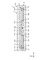
図1は、本発明の第1実施形態に係る物理量センサーを示す平面図、図2は、図1中のA−A線断面図、図3は、図1中のB−B線断面図である。図4は、図1に示す物理量センサーが備える第1固定電極部および第1可動電極部を説明するための部分拡大平面図である。図5は、図1に示す物理量センサーが備える第1弾性部を説明するための部分拡大平面図である。図6は、図1に示す物理量センサーが備える支持基板および配線パターンを説明するための平面図である。
<First embodiment>
1 is a plan view showing a physical quantity sensor according to a first embodiment of the present invention, FIG. 2 is a sectional view taken along line AA in FIG. 1, and FIG. 3 is a sectional view taken along line BB in FIG. is there. FIG. 4 is a partially enlarged plan view illustrating a first fixed electrode unit and a first movable electrode unit included in the physical quantity sensor shown in FIG. FIG. 5 is a partially enlarged plan view for explaining a first elastic portion provided in the physical quantity sensor shown in FIG. FIG. 6 is a plan view for explaining a support substrate and a wiring pattern included in the physical quantity sensor shown in FIG.
なお、各図では、説明の便宜上、互いに直交する3つの軸であるX軸、Y軸およびZ軸を矢印で図示しており、その矢印の先端側を「+(プラス)」、基端側を「−(マイナス)」としている。また、以下では、X軸に平行な方向(第2方向)を「X軸方向」、Y軸に平行な方向(第1方向)を「Y軸方向」、Z軸に平行な方向を「Z軸方向」という。また、以下では、説明の便宜上、図2および図3中の上側(+Z軸方向側)を「上」、下側(−Z軸方向側)を「下」という。 In each of the drawings, for convenience of explanation, three axes orthogonal to each other, that is, the X axis, the Y axis, and the Z axis are illustrated by arrows, and the leading end of the arrows is “+ (plus)” and the base end is Is “-(minus)”. Hereinafter, a direction parallel to the X axis (second direction) is referred to as an “X axis direction”, a direction parallel to the Y axis (first direction) is referred to as a “Y axis direction”, and a direction parallel to the Z axis is referred to as “Z direction”. "Axial direction". In the following, for convenience of description, the upper side (+ Z-axis direction side) in FIGS. 2 and 3 is referred to as “upper”, and the lower side (−Z-axis direction side) is referred to as “lower”.
図1〜3に示すように、本実施形態の物理量センサー1は、センサー素子10と、このセンサー素子10を支持している基板4と、この基板4上においてセンサー素子10に電気的に接続されている配線パターン5と、センサー素子10を覆うようにして基板4に接合されている蓋部材6と、を有している。ここで、基板4および蓋部材6は、センサー素子10を収納している空間Sを形成しているパッケージ20を構成している。以下、物理量センサー1の各部を順次説明する。
As shown in FIGS. 1 to 3, the physical quantity sensor 1 of the present embodiment is configured such that a
(センサー素子10)
図1に示すように、センサー素子10は、基板4に固定されている第1固定電極側固定部21a、第2固定電極側固定部21bおよび可動電極側固定部31と、これら固定部を平面視で囲む可動質量部32と、可動電極側固定部31と可動質量部32とを接続している弾性部33と、を有している。
(Sensor element 10)
As shown in FIG. 1, the
ここで、可動電極側固定部31、可動質量部32および弾性部33は、一体的に形成されていて、可動電極側構造体3を構成している。すなわち、センサー素子10は、互いに間隔を隔てて配置されている第1固定電極側固定部21a、第2固定電極側固定部21bおよび可動電極側構造体3を有し、可動電極側構造体3が、一体的に形成されている可動電極側固定部31、可動質量部32および弾性部33を有している。また、可動電極側固定部31は、第1可動電極側固定部31aおよび第2可動電極側固定部31bを有する。また、弾性部33は、2つの第1弾性部33aおよび2つの第2弾性部33bを有する。なお、本実施形態では、センサー素子10は、平面視で回転対称な形状であり、X軸方向およびY軸方向に関して対称な形状をなしている。
Here, the movable electrode side fixed
第1固定電極側固定部21aおよび第2固定電極側固定部21bは、Y軸方向に沿って並んで配置されている。ここで、第1固定電極側固定部21aは、センサー素子10の中心に対して+Y軸方向側に配置され、一方、第2固定電極側固定部21bは、センサー素子10の中心に対して−Y軸方向側に配置されている。
The first fixed electrode side fixed
第1固定電極側固定部21aは、基板4に接続されている接続部211aと、接続部211aから+Y軸方向に沿って延出している第1延出部212aと、第1延出部212aに接続されている第1固定電極部213aと、を有している。第1固定電極部213aは、第1延出部212aに一端が支持されている複数の第1固定電極指2131aで構成されている(図4参照)。複数の第1固定電極指2131aは、第1延出部212aから+X軸方向および−X軸方向のそれぞれの方向に沿って延出するとともにY軸方向に沿って間隔を隔てて並んで配置されていて、櫛歯状をなす「第1固定電極櫛部」を構成している。
The first fixed electrode-side fixed
同様に、第2固定電極側固定部21bは、基板4に接続されている接続部211bと、接続部211bから−Y軸方向に沿って延出している第2延出部212bと、第2延出部212bに接続されている第2固定電極部213bと、を有している。第2固定電極部213bは、前述した第1固定電極部213aに対してY軸方向に沿って並んで配置されており、第2延出部212bに一端が支持されている複数の第2固定電極指2131bで構成されている。複数の第2固定電極指2131bは、第2延出部212bから+X軸方向および−X軸方向のそれぞれの方向に沿って延出するとともにY軸方向に沿って間隔を隔てて並んで配置されていて、櫛歯状をなす「第2固定電極櫛部」を構成している。
Similarly, the second fixed electrode
一方、第1可動電極側固定部31aおよび第2可動電極側固定部31bは、Y軸方向に交差するX軸方向に沿って並んで配置されている。ここで、第1可動電極側固定部31aは、センサー素子10の中心に対して+X軸方向側に配置され、一方、第2可動電極側固定部31bは、センサー素子10の中心に対して−X軸方向側に配置されている。本実施形態では、平面視で、接続部211a、211bに対して、+X軸方向側に第1可動電極側固定部31a、−X軸方向側に第2可動電極側固定部31bが配置されている。したがって、第1固定電極側固定部21aおよび第2固定電極側固定部21bは、それぞれ、平面視で第1可動電極側固定部31aと第2可動電極側固定部31bとの間に位置している部分(接続部211a、211b)を有する。
On the other hand, the first movable electrode side fixed
第1可動電極側固定部31aは、基板4に接続されている接続部311aと、接続部311aに接続されている第1支持部312aと、を有している。第1支持部312aは、平面視でT字状をなし、接続部311aから+X軸方向に沿って延出している部分と、該部分の接続部311aとは反対の端部から+Y軸方向および−Y軸方向のそれぞれの方向に沿って延出している部分と、を有している。
The first movable electrode side fixed
同様に、第2可動電極側固定部31bは、基板4に接続されている接続部311bと、接続部311bに接続されている第2支持部312bと、を有している。第2支持部312bは、平面視でT字状をなし、接続部311bから−X軸方向に沿って延出している部分と、該部分の接続部311bとは反対の端部から+Y軸方向および−Y軸方向のそれぞれの方向に沿って延出している部分と、を有している。
Similarly, the second movable electrode side fixed
このような第1固定電極側固定部21a、第2固定電極側固定部21bおよび可動電極側固定部31は、平面視で枠状をなす可動質量部32の内側に配置されている。言い換えると、可動質量部32は、平面視で、第1固定電極側固定部21a、第2固定電極側固定部21bおよび可動電極側固定部31を囲む形状をなしている。
The first fixed electrode-side fixed
この可動質量部32は、平面視で枠状をなす枠部321と、枠部321に接続されている第1錘部323aおよび第2錘部323bと、第1錘部323aに接続されている第1可動電極部322aと、第2錘部323bに接続されている第2可動電極部322bと、を有している。
The
枠部321は、センサー素子10の外縁部を構成しており、前述したように、枠部321の内側には、第1固定電極側固定部21a、第2固定電極側固定部21bおよび可動電極側固定部31が配置されている。
The
第1錘部323aは、枠部321の内側にて枠部321に接続され、平面視で第1固定電極側固定部21a(主に第1固定電極部213a)の周囲を囲むように形成されている。一方、第2錘部323bは、枠部321の内側にて枠部321に接続され、平面視で第2固定電極側固定部21b(主に第2固定電極部213b)の周囲を囲むように形成されている。
The
第1可動電極部322aは、前述した第1固定電極部213aに対向している部分を有する。具体的には、第1可動電極部322aは、第1錘部323aに一端が支持されていて、前述した第1固定電極部213aの複数の第1固定電極指2131a(第1固定電極櫛部)に対して間隔dを隔てて噛み合うように第1錘部323aから延出して配置されている複数の第1可動電極指3221aで構成されている(図4参照)。複数の第1可動電極指3221aは、第1錘部323aからX軸方向に沿って延出するとともにY軸方向に沿って間隔を隔てて並んで配置されていて、櫛歯状をなす「第1可動電極櫛部」を構成している。
The first
同様に、第2可動電極部322bは、前述した第2固定電極部213bに対向している部分を有する。具体的には、第2可動電極部322bは、第2錘部323bに一端が支持されていて、前述した第2固定電極部213bの複数の第2固定電極指2131bに対して間隔を隔てて噛み合うように第2錘部323bから延出して配置されている複数の第2可動電極指3221bで構成されている。複数の第2可動電極指3221bは、第2錘部323bからX軸方向に沿って延出するとともにY軸方向に沿って間隔を隔てて並んで配置されていて、櫛歯状をなす「第2可動電極櫛部」を構成している。
Similarly, the second
このような可動質量部32は、前述した第1可動電極側固定部31aに対して2つの第1弾性部33aを介して支持されているとともに、前述した第2可動電極側固定部31bに対して2つの第2弾性部33bを介して支持されている。したがって、平面視で、枠状をなす枠部321の内側には、前述した第1固定電極側固定部21a、第2固定電極側固定部21b、第1可動電極側固定部31aおよび第2可動電極側固定部31bだけでなく、2つの第1弾性部33aおよび2つの第2弾性部33bも配置されることとなる。
Such a
2つの第1弾性部33aは、それぞれ、可動質量部32をY軸方向に変位可能に第1可動電極側固定部31aと可動質量部32とを接続している。2つの第1弾性部33aのうちの一方の第1弾性部33aは、第1可動電極側固定部31aが有する第1支持部312aの+Y軸方向側の端部に接続され、他方の第1弾性部33aは、第1支持部312aの−Y軸方向側の端部に接続されている。同様に、2つの第2弾性部33bは、それぞれ、可動質量部32をY軸方向に変位可能に第2可動電極側固定部31bと可動質量部32とを接続している。2つの第2弾性部33bのうちの一方の第2弾性部33bは、第2可動電極側固定部31bが有する第2支持部312bの+Y軸方向側の端部に接続され、他方の第2弾性部33bは、第2支持部312bの−Y軸方向側の端部に接続されている。
The two first
第1支持部312aの+Y軸方向側の端部に接続された第1弾性部33aと、第2支持部312bの+Y軸方向側の端部に接続された第2弾性部33bとは、X軸方向に互いに接近と離間とを繰り返すように蛇行しながらそれぞれY軸方向に延びている形状をなしている。同様に、第1支持部312aの−Y軸方向側の端部に接続された第1弾性部33aと、第2支持部312bの−Y軸方向側の端部に接続された第2弾性部33bとは、X軸方向に互いに接近と離間とを繰り返すように蛇行しながらそれぞれY軸方向に延びている形状をなしている。
The first
図5に示すように、第1弾性部33aは、X軸方向に沿って延びている部分331a(梁)および部分332a(梁)と、これらの部分331a、332aの端部同士を連結している部分333a(連結部)と、を有している。同様に、第2弾性部33bは、X軸方向に沿って延びている部分331b(梁)および部分332b(梁)と、これらの部分331b、332bの端部同士を連結している部分333b(連結部)と、を有している。
As shown in FIG. 5, the first
なお、第1弾性部33aおよび第2弾性部33bの形状は、可動質量部32をY軸方向に変位可能とすることができれば、前述したものに限定されず、例えば、X軸方向に沿って延びている1つの梁で構成されていてもよいし、3本以上の梁とこれらの梁を連結する2つ以上の連結部とで構成されていてもよい。
Note that the shapes of the first
以上説明したような第1固定電極側固定部21a、第2固定電極側固定部21bおよび可動電極側構造体3の構成材料としては、それぞれ、特に限定されないが、例えば、リン、ボロン等の不純物をドープされることにより導電性が付与されたシリコン材料(単結晶シリコン、ポリシリコン等)を用いるのが好ましい。
The constituent materials of the first fixed electrode-side fixed
また、第1固定電極側固定部21a、第2固定電極側固定部21bおよび可動電極側構造体3は、1つの基板(例えばシリコン基板)をエッチングすることより一括して形成することができる。この場合、センサー素子10の各部の厚さを簡単かつ高精度に揃えることができる。また、シリコンはエッチングにより高精度に加工することができる。
Further, the first fixed electrode-side fixed
以上説明したように構成されたセンサー素子10では、センサー素子10が検出軸方向であるY軸方向の加速度を受けると、第1弾性部33aおよび第2弾性部33bの弾性変形を伴って、可動質量部32がY軸方向に変位する。すると、第1固定電極部213aの第1固定電極指2131aと第1可動電極部322aの第1可動電極指3221aとの間の距離、および、第2固定電極部213bの第2固定電極指2131bと第2可動電極部322bの第2可動電極指3221bとの間の距離がそれぞれ変化する。
In the
したがって、これらの間の静電容量に基づいて、センサー素子10が受けた加速度の大きさを検出することができる。本実施形態では、第1固定電極指2131aと第1可動電極指3221aとの間の距離、および、第2固定電極指2131bと第2可動電極指3221bとの間の距離は、一方の距離が大きくなると、他方の距離が小さくなる。そのため、第1固定電極指2131aと第1可動電極指3221aとの間の静電容量、および、第2固定電極指2131bと第2可動電極指3221bとの間の静電容量も、一方の静電容量が大きくなると、他方の静電容量が小さくなる。したがって、第1固定電極部213aの第1固定電極指2131aと第1可動電極部322aの第1可動電極指3221aとの間の静電容量に基づく信号と、第2固定電極部213bの第2固定電極指2131bと第2可動電極部322bの第2可動電極指3221bとの間の静電容量に基づく信号とを差動演算する。これにより、検出軸方向以外の可動質量部32の変位に伴う信号成分を除去してノイズを低減しつつ、センサー素子10が受けた加速度に応じた信号を出力することができる。
Therefore, the magnitude of the acceleration received by the
(基板)
基板4(支持基板)は、板状をなし、X軸およびY軸を含む平面であるXY平面(基準面)に沿って配置されている。この基板4の上面(センサー素子10が設けられている側の面)には、図2および図3に示すように、凹部41が設けられている。この凹部41は、センサー素子10の可動部分(具体的には、可動質量部32等)が基板4に接触するのを防止する機能を有する。これにより、センサー素子10の駆動を許容しつつ、基板4がセンサー素子10を支持することができる。
(substrate)
The substrate 4 (support substrate) has a plate shape and is arranged along an XY plane (reference plane) which is a plane including the X axis and the Y axis. On the upper surface of the substrate 4 (the surface on which the
また、図4に示すように、基板4の上面には、凹部41の底面から突出している第1突起部(第1固定電極側固定部用の突起部)42a、第2突起部(第1固定電極側固定部用の突起部)42b、2つの第3突起部(第1可動電極側固定部用の突起部)43a、および、2つの第4突起部(第2可動電極側固定部用の突起部)43bが設けられている。さらに、基板4の上面には、凹部41の底面から突出している4つの突起部44、および、4つの突起部45が設けられている。
As shown in FIG. 4, on the upper surface of the substrate 4, a first protruding portion (a protruding portion for the first fixed electrode side fixing portion) 42 a protruding from the bottom surface of the
第1突起部42a、第2突起部42b、第3突起部43aおよび第4突起部43bは、それぞれ、センサー素子10の可動部分を基板4に対して浮遊(離間)させた状態でセンサー素子10を支持する機能を有する。
The first protruding
第1突起部42aには、前述した第1固定電極側固定部21aの接続部211aが接合されている。第2突起部42bには、前述した第2固定電極側固定部21bの接続部211bが接合されている。2つの第3突起部43aには、前述した第1可動電極側固定部31aの接続部311aが接合されている。2つの第4突起部43bには、前述した第2可動電極側固定部31bの接続部311bが接合されている。
The
4つの突起部44および4つの突起部45は、センサー素子10の浮遊部分(特に可動質量部32)が基板4に張り付くのを防止する機能を有する。
Four
具体的に説明すると、4つの突起部44は、平面視で、前述した可動質量部32の外周部(より具体的には、平面視で四角形の外形を有する枠部321の4つの角部)に重なる位置に配置されている。これにより、可動質量部32が基板4に張り付くのを効果的に低減することができる。
More specifically, the four
また、4つの突起部45は、平面視で、後述する配線パターン5から基板4の上面が露出する部分(陽極接合時に大きな電界がかかる部分)近傍であって、可動質量部32に重なる位置に配置されている。これにより、可動質量部32が基板4に張り付くのを効果的に低減することができる。
In addition, the four
また、基板4の構成材料としては、特に限定されないが、絶縁性を有する基板材料を用いることが好ましく、具体的には、石英基板、サファイヤ基板、ガラス基板を用いるのが好ましく、特に、アルカリ金属イオン(可動イオン)を含むガラス材料(例えば、パイレックスガラス(登録商標)のような硼珪酸ガラス)を用いるのが好ましい。これにより、センサー素子10や蓋部材6がシリコンを主材料として構成されている場合、これらを基板4に対して陽極接合することができる。
Further, the constituent material of the substrate 4 is not particularly limited, but it is preferable to use a substrate material having an insulating property. Specifically, it is preferable to use a quartz substrate, a sapphire substrate, or a glass substrate. It is preferable to use a glass material containing ions (mobile ions) (for example, borosilicate glass such as Pyrex glass (registered trademark)). Thereby, when the
なお、図示では、基板4は、1部材で構成されているが、2以上の部材を接合して構成されていてもよい。例えば、枠状の部材と板状の部材とを貼り合わせることにより、基板4が構成されていてもよい。 In the drawing, the substrate 4 is formed of one member, but may be formed by joining two or more members. For example, the substrate 4 may be configured by bonding a frame-shaped member and a plate-shaped member.
また、基板4は、例えば、フォトリソグラフィー法およびエッチング法等を用いて形成することができる。 The substrate 4 can be formed using, for example, a photolithography method, an etching method, or the like.
(配線パターン)
図6に示すように、配線パターン5は、前述した基板4の上面上に設けられている。この配線パターン5は、前述した第1固定電極側固定部21aに電気的に接続されている第1固定電極側配線51aと、第2固定電極側固定部21bに電気的に接続されている第2固定電極側配線51bと、可動電極側固定部31に電気的に接続されている可動電極側配線52a、52b、53と、を有している。
(Wiring pattern)
As shown in FIG. 6, the wiring pattern 5 is provided on the upper surface of the substrate 4 described above. The wiring pattern 5 includes a first fixed electrode-
第1固定電極側配線51aは、前述した第1突起部42a付近から+Y軸方向側に延びて配置されている。第1固定電極側配線51aの−Y軸方向側の端部は、第1コンタクト部54aを介して、第1固定電極側固定部21aに接続されている。また、第1固定電極側配線51aの+Y軸方向側の端部は、パッケージ20の外部へ引き出されて、図示しない外部端子に電気的に接続されている。同様に、第2固定電極側配線51bは、前述した第2突起部42b付近から−Y軸方向側に延びて配置されている。第2固定電極側配線51bの+Y軸方向側の端部は、第2コンタクト部54bを介して、第2固定電極側固定部21bに接続されている。また、第2固定電極側配線51bの−Y軸方向側の端部は、パッケージ20の外部へ引き出されて、図示しない外部端子に電気的に接続されている。ここで、第1固定電極側固定部21aの第1コンタクト部54aと接続している部分は、前述した第1固定電極側固定部21aの基板4と接続している接続部211aの一部を構成しているとも言える。同様に、第2固定電極側固定部21bの第2コンタクト部54bと接続している部分は、前述した第2固定電極側固定部21bの基板4と接続している接続部211bの一部を構成しているとも言える。
The first fixed electrode-
可動電極側配線52a、52bは、それぞれ、平面視で、センサー素子10の可動質量部32とできるだけ重なるように配置されている。可動電極側配線52aは、第1固定電極側配線51aおよび第2固定電極側配線51bに対して+X軸方向側に配置されている。可動電極側配線52bは、第1固定電極側配線51aおよび第2固定電極側配線51bに対して−X軸方向側に配置されている。
The movable
可動電極側配線53は、第1突起部42aと第2突起部42bとの間に配置されている部分を有し、可動電極側配線52aと可動電極側配線52bとを接続している。そして、可動電極側配線53は、第3コンタクト部55aを介して、第1可動電極側固定部31aに接続されているとともに、第4コンタクト部55bを介して、第2可動電極側固定部31bに接続されている。ここで、第1可動電極側固定部31aの第3コンタクト部55aと接続している部分は、前述した第1可動電極側固定部31aの基板4と接続している接続部311aの一部を構成しているとも言える。同様に、第2可動電極側固定部31bの第4コンタクト部55bと接続している部分は、前述した第2可動電極側固定部31bの基板4と接続している接続部311bの一部を構成しているとも言える。
The movable
このような配線パターン5の構成材料としては、それぞれ、導電性を有するものであれば、特に限定されず、各種電極材料を用いることができ、例えば、ITO(酸化インジウムスズ)、ZnO(酸化亜鉛)等の透明電極材料、金(Au)、金合金、白金(Pt)、アルミニウム(Al)、アルミニウム合金、銀(Ag)、銀合金、クロム(Cr)、クロム合金、銅(Cu)、モリブデン(Mo)、ニオブ(Nb)、タングステン(W)、鉄(Fe)、チタン(Ti)、コバルト(Co)、亜鉛(Zn)、ジルコニウム(Zr)等の金属材料、シリコン(Si)等の半導体材料を用いることができる。 The constituent material of the wiring pattern 5 is not particularly limited as long as it has conductivity, and various electrode materials can be used. For example, ITO (indium tin oxide), ZnO (zinc oxide) can be used. ), Gold (Au), gold alloy, platinum (Pt), aluminum (Al), aluminum alloy, silver (Ag), silver alloy, chromium (Cr), chromium alloy, copper (Cu), molybdenum (Mo), niobium (Nb), tungsten (W), iron (Fe), titanium (Ti), cobalt (Co), zinc (Zn), zirconium (Zr) and other metal materials, and silicon (Si) and other semiconductors Materials can be used.
また、配線パターン5は、前述したような材料をスパッタリング法、蒸着法等の気相成膜法を用いて成膜した膜を、フォトリソグラフィー法およびエッチング法等を用いてパターニングすることによって一括して形成される。なお、基板4がシリコンのような半導体材料で構成されている場合には、基板4と配線パターン5との間に絶縁層を設けることが好ましい。かかる絶縁層の構成材料としては、例えば、SiO2(酸化ケイ素)、AlN(窒化アルミ)、SiN(窒化ケイ素)等を用いることができる。 In addition, the wiring pattern 5 is formed by patterning a film formed from the above-described material using a vapor deposition method such as a sputtering method or a vapor deposition method using a photolithography method, an etching method, or the like. Formed. When the substrate 4 is made of a semiconductor material such as silicon, it is preferable to provide an insulating layer between the substrate 4 and the wiring pattern 5. As a constituent material of such an insulating layer, for example, SiO 2 (silicon oxide), AlN (aluminum nitride), SiN (silicon nitride) and the like can be used.
また、各コンタクト部の構成材料としては、それぞれ、導電性を有するものであれば、特に限定されず、配線パターン5と同様、各種電極材料を用いることができるが、例えば、Au、Pt、Ag、Cu、Al等の金属単体またはこれらを含む合金等の金属が好適に用いられる。このような金属を用いて各コンタクト部を構成することにより、配線パターン5とセンサー素子10との間の接点抵抗を小さくすることができる。
The material of each contact portion is not particularly limited as long as it has conductivity, and various electrode materials can be used as in the case of the wiring pattern 5. For example, Au, Pt, Ag , Cu, Al, etc., or a metal such as an alloy containing them is preferably used. By configuring each contact portion using such a metal, the contact resistance between the wiring pattern 5 and the
(蓋部材)
図2および図3に示すように、蓋部材6は、前述したセンサー素子10を保護する機能を有する。
(Lid member)
As shown in FIGS. 2 and 3, the lid member 6 has a function of protecting the
この蓋部材6は、前述した基板4に接合され、基板4との間にセンサー素子10を収納する空間Sを形成する。
The lid member 6 is joined to the above-described substrate 4 and forms a space S for accommodating the
具体的に説明すると、この蓋部材6は、板状をなし、その下面(センサー素子10側の面)に凹部61が設けられている。この凹部61は、センサー素子10の可動部分の変位を許容するように形成されている。
More specifically, the lid member 6 has a plate shape, and a
そして、蓋部材6の下面の凹部61よりも外側の部分は、前述した基板4の上面に接合されている。蓋部材6と基板4との接合方法としては、特に限定されず、例えば、接着剤を用いた接合方法、陽極接合法、直接接合法等を用いることができる。
The portion of the lower surface of the lid member 6 outside the
また、蓋部材6の構成材料としては、前述したような機能を発揮し得るものであれば、特に限定されないが、例えば、シリコン材料、ガラス材料等を好適に用いることができる。 Further, the constituent material of the lid member 6 is not particularly limited as long as it can exhibit the above-described functions, and for example, a silicon material, a glass material, or the like can be suitably used.
以上説明したような物理量センサー1によれば、平面視で、可動質量部32を枠体化し、かつ、その可動質量部32の枠部321の内側に、第1固定電極側固定部21aおよび第2固定電極側固定部21bと、第1可動電極側固定部31aおよび第2可動電極側固定部31bとを配置することができる。これにより、第1固定電極側固定部21aと第2固定電極側固定部21bとの間の距離、および、第1可動電極側固定部31aと第2可動電極側固定部31bとの間の距離をそれぞれ短くすることができる。より具体的には、接続部211aと接続部211bとの距離、および、接続部311aと接続部311bとの距離をそれぞれ短くすることができる。そのため、基板4が温度変化に伴って反ってしまっても、電極部間の歪み差を低減することができる。その結果、温度特性を優れたものとすることができる。しかも、可動質量部32を枠体化し、可動質量部32が変位する方向(検出軸方向)と同じ方向であるY軸方向に沿うように第1固定電極部213aおよび第2固定電極部213bを配置していることにより、第1固定電極部213aおよび第2固定電極部213b間の距離を短くすることができる。その結果、物理量センサー1の感度をより高めることができる。
According to the physical quantity sensor 1 described above, the
ここで、温度変化による基板4の反りは、例えば、基板4とセンサー素子10または蓋部材6との線膨張係数差に起因して生じる。このため、特にこのような線膨張係数差がある場合に、前述したような温度特性を向上させる効果を顕著に生じさせることができる。
Here, the warpage of the substrate 4 due to the temperature change occurs due to, for example, a difference in linear expansion coefficient between the substrate 4 and the
また、前述したように、第1固定電極側固定部21aの接続部211aおよび第2固定電極側固定部21bの接続部211bは、それぞれ、平面視で第1可動電極側固定部31aの接続部311aと第2可動電極側固定部31bの接続部311bとの間に位置している。そして、接続部211aと接続部211bとの離間距離は、接続部311aと接続部311bとの離間距離よりも短くなっている。すなわち、第1可動電極側固定部31aと第2可動電極側固定部31bとの離間距離は、第1固定電極側固定部21aと第2固定電極側固定部21bとの離間距離よりも長くなっている。
In addition, as described above, the
これにより、基板4がY軸方向に反ったときに、その基板4の反りの影響を第1固定電極側固定部21aおよび第2固定電極側固定部21bが受けることを低減することができる。その結果、温度特性をより優れたものとすることができる。
Accordingly, when the substrate 4 warps in the Y-axis direction, it is possible to reduce the influence of the warpage of the substrate 4 on the first fixed electrode
また、物理量センサー1は、各第1可動電極指3221a、各第2可動電極指3221b、各第1固定電極指2131aおよび各第2固定電極指2131bが検出軸方向に対して直交するX軸方向に沿って延びているため、可動質量部32の変位に伴う、第1固定電極部213aと第1可動電極部322aとの間、および、第2固定電極部213bと第2可動電極部322bとの間のそれぞれの静電容量変化を大きくすることができる。そのため、物理量センサー1の高感度化を図ることができる。
The physical quantity sensor 1 has an X-axis direction in which each of the first
また、第1延出部212aおよび第2延出部212bのそれぞれが検出軸方向であるY軸方向に沿って延びているため、第1可動電極指3221a、第2可動電極指3221b、第1固定電極指2131aおよび第2固定電極指2131bのそれぞれの数を効率的に多くすることができる。そのため、可動質量部32の変位に伴う、第1固定電極部213aと第1可動電極部322aとの間、および、第2固定電極部213bと第2可動電極部322bとの間のそれぞれの静電容量変化をより大きくすることができる。
Further, since each of the
また、前述したように、第1延出部212aが第1可動電極側固定部31aおよび第2可動電極側固定部31bに対してY軸方向での一方側に配置され、第2延出部212bが第1可動電極側固定部31aおよび第2可動電極側固定部31bに対してY軸方向での他方側に配置されている。これにより、前述したように、第1固定電極部213aと第1可動電極部322aとの間の静電容量変化による信号と、第2固定電極部213bと第2可動電極部322bとの間の静電容量変化による信号とを差動演算することにより、ノイズを低減することができる。
Further, as described above, the
また、第1延出部212aは、平面視で、第1固定電極指2131aに電気的に接続されている第1固定電極側配線51aと重なる部分を有する。同様に、第2延出部212bは、平面視で、第2固定電極指2131bに電気的に接続されている第2固定電極側配線51bと重なる部分を有する。ここで、第1延出部212aと第1固定電極側配線51aとが互いに同電位であり、また、第2延出部212bと第2固定電極側配線51bとが互いに同電位である。そのため、第1延出部212aと第1固定電極側配線51aとを平面視で重ねるとともに第2延出部212bと第2固定電極側配線51bとを平面視で重ねることで、基板4と第1延出部212aおよび第2延出部212bとの間に生じる寄生容量を低減することができる。その結果、物理量センサー1の検出特性を優れたものとすることができる。
Further, the
また、平面視で、第1可動電極指3221aの先端部が、第1可動電極指3221aに電気的に接続されている可動電極側配線52aに重なり、第2可動電極指3221bの先端部が、第2可動電極指3221bに電気的に接続されている可動電極側配線52bと重なっている。これにより、例えば、第1固定電極側固定部21aおよび第2固定電極側固定部21bを含む構造体であるセンサー素子10と基板4とを陽極接合する際に、第1可動電極指3221aの先端部がこれと同電位の可動電極側配線52aに対向することとなるとともに、第2可動電極指3221bの先端部がこれと同電位の可動電極側配線52bに対向することとなる。そのため、その陽極接合の際に、第1可動電極指3221aおよび第2可動電極指3221bの先端部と基板4との間に生じる電界を低減し、その結果、各第1可動電極指3221aおよび各第2可動電極指3221bが基板4に張り付くのを防止または低減することができる。
Further, in plan view, the tip of the first
また、前述したように、第1可動電極側固定部31aの接続部311aおよび第2可動電極側固定部31bの接続部311bの双方が可動電極側配線53に接続されている。これにより、互いに同電位となる第1可動電極側固定部31aおよび第2可動電極側固定部31bを含む構造体である可動電極側構造体3と可動電極側配線53との電気的なコンタクトを第1コンタクト部54aおよび第2コンタクト部54bによる複数箇所で行うことができる。そのため、当該コンタクトの信頼性を高めることができる。
Further, as described above, both the
また、前述したように、導電性の第1コンタクト部54aが接続部311aと可動電極側配線53との間にこれら両者に接して設けられているとともに、導電性の第2コンタクト部54bが接続部311bと可動電極側配線53との間に両者に接して設けられている。これにより、可動電極側構造体3と可動電極側配線53との電気的なコンタクトの信頼性を高めることができる。
Further, as described above, the conductive
また、前述したように、基板4の主面には、平面視で可動質量部32と重なって複数の突起部44および複数の突起部45が設けられている。これにより、可動質量部32の面外方向での移動を突起部44、45により規制することができ、その結果、可動質量部32が基板4に張り付くのを防止または低減することができる。
Further, as described above, the main surface of the substrate 4 is provided with the plurality of
また、前述したように、弾性部33が、可動質量部32をY軸方向に変位可能に第1可動電極側固定部31aと可動質量部32とを接続している第1弾性部33aと、可動質量部32をY軸方向に変位可能に第2可動電極側固定部31bと可動質量部32とを接続している第2弾性部33bと、を有している。このような弾性部33によって、可動質量部32をより安定して支持することができる。そのため、物理量センサー1の特性を高めることができる。
Further, as described above, the
また、前述したように、第1支持部312aが接続部311aから+X軸方向に延出する部分を有し、第2支持部312bが接続部311bから−X軸方向に延出する部分を有している。このため、第1支持部312aと第1弾性部33aとの接続部分と、第2支持部312bと第2弾性部33bとの接続部分の間の距離を大きくすることができる。そのため、可動質量部32の面外方向(Z軸方向)での変位を低減することや、面外方向を軸とした面内の捩れ振動を低減することができる。そのため、物理量センサー1の耐衝撃性を高めることができる。
Further, as described above, the
<第2実施形態>
図7は、本発明の第2実施形態に係る物理量センサーを示す平面図である。
<Second embodiment>
FIG. 7 is a plan view showing a physical quantity sensor according to the second embodiment of the present invention.
本実施形態に係る物理量センサーは、第1固定電極側固定部の接続部、第2固定電極側固定部の接続部、第1可動電極側固定部の接続部および第2可動電極側固定部の接続部の配置が異なる以外は、前述した第1実施形態に係る物理量センサーと同様である。 The physical quantity sensor according to the present embodiment includes a connection portion of the first fixed electrode side fixed portion, a connection portion of the second fixed electrode side fixed portion, a connection portion of the first movable electrode side fixed portion, and a connection portion of the second movable electrode side fixed portion. It is the same as the physical quantity sensor according to the above-described first embodiment except that the arrangement of the connection portions is different.
なお、以下の説明では、第2実施形態に関し、前述した実施形態との相違点を中心に説明し、同様の事項に関してはその説明を省略する。また、図7では、前述した第1実施形態と同様の構成について、同一符号を付している。 In the following description, the second embodiment will be described focusing on differences from the above-described embodiment, and the description of the same items will be omitted. In FIG. 7, the same reference numerals are given to the same components as those in the above-described first embodiment.
図7に示すように、本実施形態の物理量センサー1Aが有するセンサー素子10Aは、第1固定電極側固定部21aと、第2固定電極側固定部21bと、可動電極側構造体3Aと、を有する。可動電極側構造体3Aは、第1可動電極側固定部31cおよび第2可動電極側固定部31dを有する第1可動電極側固定部31Aと、可動質量部32と、弾性部33とを有する。
As shown in FIG. 7, the sensor element 10A included in the
第1可動電極側固定部31cは、基板4に接続されている接続部311cと、接続部311cに接続されている第1支持部312aと、を有している。同様に、第2可動電極側固定部31dは、基板4に接続されている接続部311dと、接続部311dに接続されている第2支持部312bと、を有している。
The first movable electrode side fixed
本実施形態では、接続部311cおよび接続部311dが、平面視で、第1固定電極側固定部21aが有する接続部211aと第2固定電極側固定部21bが有する接続部211bとの間に位置している。そして、接続部311cと接続部311dとの離間距離が、接続部211aと接続部211bとの離間距離よりも短くなっている。すなわち、第1可動電極側固定部31cと第2可動電極側固定部31dとの離間距離が、第1固定電極側固定部21aと第2固定電極側固定部21bとの離間距離よりも短くなっている。これにより、基板4がX軸方向に反ったときに、その基板4の反りの影響を第1可動電極側固定部31cおよび第2可動電極側固定部31dが受けることを低減することができる。その結果、温度特性をより優れたものとすることができる。
In the present embodiment, the
以上説明したような第2実施形態に係る物理量センサー1Aによっても、優れた温度特性を実現することができる。
Excellent temperature characteristics can also be realized by the
<第3実施形態>
図8は、本発明の第3実施形態に係る物理量センサーを示す平面図である。
<Third embodiment>
FIG. 8 is a plan view showing a physical quantity sensor according to the third embodiment of the present invention.
本実施形態に係る物理量センサーは、可動電極側固定部の構成が異なる以外は、前述した第1実施形態に係る物理量センサーと同様である。 The physical quantity sensor according to the present embodiment is the same as the physical quantity sensor according to the above-described first embodiment except that the configuration of the movable electrode side fixed portion is different.
なお、以下の説明では、第3実施形態に関し、前述した実施形態との相違点を中心に説明し、同様の事項に関してはその説明を省略する。また、図8では、前述した第1実施形態と同様の構成について、同一符号を付している。 In the following description, the third embodiment will be described with a focus on differences from the above-described embodiment, and a description of similar items will be omitted. In FIG. 8, the same components as those in the first embodiment are denoted by the same reference numerals.
(センサー素子10B)
図8に示すように、本実施形態の物理量センサー1Bが有するセンサー素子10Bは、第1固定電極側固定部21aと、第2固定電極側固定部21bと、可動電極側構造体3Bと、を有する。可動電極側構造体3Bは、可動電極側固定部31Bと、可動質量部32と、弾性部33とを有している。
(Sensor element 10B)
As shown in FIG. 8, the sensor element 10B included in the physical quantity sensor 1B of the present embodiment includes a first fixed electrode side fixed
可動電極側固定部31Bは、センサー素子10Bの中心に対して+X軸方向側に配置された第1可動電極側固定部31eと、センサー素子10Bの中心に対して−X軸方向側に配置された第2可動電極側固定部31fと、第1可動電極側固定部31eおよび第2可動電極側固定部31fを連結する連結部34と、を有している。第1可動電極側固定部31e、第2可動電極側固定部31fおよび連結部34は、一体的に形成されている。
The movable electrode
第1可動電極側固定部31eは、基板4に接続されている基部311eと、基部311eに接続されている第1支持部312aと、を有している。同様に、第2可動電極側固定部31fは、基板4に接続されている基部311fと、基部311fに接続されている第2支持部312bと、を有している。
The first movable electrode side fixed
連結部34は、平面視で、可動質量部32の重心O32上を通り、第1固定電極側固定部21aが有する接続部211aと第2固定電極側固定部21bが有する接続部211bとの間を通ってY軸方向に沿って延びていて、基部311eと基部311fとを接続している。言い換えると、可動電極側固定部31Bは、平面視で、第1固定電極側固定部21aが有する接続部211aと第2固定電極側固定部21bが有する接続部211bとの間に位置している部分(連結部34)を備えている。このような連結部34を備えることにより、第1可動電極側固定部31eと第2可動電極側固定部31fとの電位差が生じるのを低減し、安定したセンサー特性を実現することができる。
The connecting
(基板4B)
基板4Bの上面には、第1突起部(第1固定電極側固定部用の突起部)42a、第2突起部(第1固定電極側固定部用の突起部)42bおよび1つの第3突起部(第1可動電極側固定部用の突起部)43cが設けられている。
(Substrate 4B)
On the upper surface of the substrate 4B, a first protrusion (a protrusion for the first fixed electrode-side fixing portion) 42a, a second protrusion (a protrusion for the first fixed electrode-side fixing portion) 42b, and one third protrusion A portion (projection portion for the first movable electrode side fixed portion) 43c is provided.
第1突起部42a、第2突起部42bおよび第3突起部43cは、それぞれ、センサー素子10Bの可動部分を基板4Bに対して浮遊(離間)させた状態でセンサー素子10Bを支持する機能を有する。
Each of the
第1突起部42aには、接続部211aが接合され、第2突起部42bには、接続部211bが接合されている。
The
第3突起部43cには、前述した可動電極側固定部31Bの連結部34が接合されている。すなわち、連結部34は、第3突起部43cに接続される接続部としての機能を有する。
The connecting
本実施形態では、前述したように、連結部34が、可動質量部32の重心O32上に位置しており、その連結部34が基板4Bに接続されている。このように、平面視で、重心O32上または重心O32近傍に位置する連結部34にて基板4Bに配置することができることで、基板4Bの反りの影響を可動電極側固定部31Bが受けることをより低減することができる。その結果、温度特性をより優れたものとすることができる。
In the present embodiment, as described above, the connecting
特に、前述したように、平面視で、連結部34を接続部211aと接続部211bとの間に位置させることで、連結部34(可動電極側固定部31Bの一部)を可動質量部32の重心O32上または重心O32近傍に配置させ易くなる。その結果、前述したように、温度特性をより高めることができる。
In particular, as described above, by positioning the connecting
以上説明したような第3実施形態に係る物理量センサー1Bによっても、優れた温度特性を実現することができる。 Excellent temperature characteristics can be realized also by the physical quantity sensor 1B according to the third embodiment described above.
<第4実施形態>
図9は、本発明の第4実施形態に係る物理量センサーを示す平面図である。
<Fourth embodiment>
FIG. 9 is a plan view showing a physical quantity sensor according to the fourth embodiment of the present invention.
本実施形態に係る物理量センサーは、第1固定電極側固定部21aの接続部211a、第2固定電極側固定部21bの接続部211b、第1可動電極側固定部31aの接続部311aおよび第2可動電極側固定部31bの接続部311bの構成が異なる以外は、前述した第1実施形態に係る物理量センサーと同様である。
The physical quantity sensor according to the present embodiment includes a
なお、以下の説明では、第4実施形態に関し、前述した実施形態との相違点を中心に説明し、同様の事項に関してはその説明を省略する。また、図9では、前述した第1実施形態と同様の構成について、同一符号を付している。 In the following description, the fourth embodiment will be described with a focus on differences from the above-described embodiment, and a description of similar items will be omitted. In FIG. 9, the same reference numerals are given to the same components as those in the above-described first embodiment.
図9に示すように、本実施形態の物理量センサー1Cが有するセンサー素子10Cは、第1固定電極側固定部21cと、第2固定電極側固定部21dと、可動電極側構造体3Cと、を有する。可動電極側構造体3Cは、第1可動電極側固定部31gおよび第2可動電極側固定部31hを有する可動電極側固定部31Cと、可動質量部32と、弾性部33とを有する。
As shown in FIG. 9, the sensor element 10C included in the physical quantity sensor 1C of the present embodiment includes a first fixed electrode side fixed
第1固定電極側固定部21cは、基板4に接続されている接続部211cと、接続部211cから延出している第1延出部212aと、第1延出部212aに接続されている第1固定電極部213aと、を有している。同様に、第2固定電極側固定部21dは、基板4に接続されている接続部211dと、接続部211dから延出している第2延出部212bと、第2延出部212bに接続されている第2固定電極部213bと、を有している。
The first fixed electrode-
第1可動電極側固定部31gは、基板4に接続されている接続部311gと、接続部311gに接続されている第1支持部312aと、を有している。同様に、第2可動電極側固定部31hは、基板4に接続されている接続部311hと、接続部311hに接続されている第2支持部312bと、を有している。
The first movable electrode side fixed
本実施形態では、接続部211c、211d、311g、311hが、平面視で、−X軸方向側から+X軸方向側へ、接続部311h、接続部211c、接続部211d、接続部311gの順で、X軸方向に沿って並んで配置されている。このような接続部211c、211d、311g、311hの配置であっても、前述した第1実施形態と同様に、接続部211cと接続部211dとの距離、および、接続部311gと接続部311hとの距離をそれぞれ短くすることができる。そのため、基板4が温度変化に伴って反ってしまっても、センサー素子10が基板4の反りの影響を受けるのを低減し、その結果、温度特性を優れたものとすることができる。特に、Y軸方向の基板4の反りの影響を第1可動電極側固定部31gおよび第2可動電極側固定部31hが受けることを低減することができる。
In the present embodiment, the
以上説明したような第4実施形態に係る物理量センサー1Cによっても、優れた温度特性を実現することができる。 Excellent temperature characteristics can also be realized by the physical quantity sensor 1C according to the fourth embodiment as described above.
2.電子機器
次いで、物理量センサー1を用いた電子機器について、図10〜図12に基づき、詳細に説明する。
2. Electronic Device Next, an electronic device using the physical quantity sensor 1 will be described in detail with reference to FIGS.
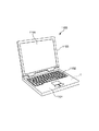
図10は、本発明の電子機器の一例であるモバイル型のパーソナルコンピューターの構成を模式的に示す斜視図である。 FIG. 10 is a perspective view schematically showing a configuration of a mobile personal computer as an example of the electronic apparatus of the present invention.
この図において、パーソナルコンピューター1100は、キーボード1102を備えた本体部1104と、表示部1108を備えた表示ユニット1106とにより構成され、表示ユニット1106は、本体部1104に対しヒンジ構造部を介して回動可能に支持されている。このようなパーソナルコンピューター1100には、ジャイロセンサーとして機能する物理量センサー1が内蔵されている。
In this figure, a
図11は、本発明の電子機器の一例である携帯電話機の構成を模式的に示す斜視図である。 FIG. 11 is a perspective view schematically showing a configuration of a mobile phone as an example of the electronic apparatus of the present invention.
この図において、携帯電話機1200は、複数の操作ボタン1202、受話口1204および送話口1206を備え、操作ボタン1202と受話口1204との間には、表示部1208が配置されている。このような携帯電話機1200には、ジャイロセンサーとして機能する物理量センサー1が内蔵されている。
In this figure, a
図12は、本発明の電子機器の一例であるディジタルスチルカメラの構成を示す斜視図である。なお、この図には、外部機器との接続についても簡易的に示されている。ここで、通常のカメラは、被写体の光像により銀塩写真フィルムを感光するのに対し、ディジタルスチルカメラ1300は、被写体の光像をCCD(Charge Coupled Device)などの撮像素子により光電変換して撮像信号(画像信号)を生成する。
FIG. 12 is a perspective view showing a configuration of a digital still camera which is an example of the electronic apparatus of the present invention. In this figure, connection with an external device is also simply shown. Here, a normal camera exposes a silver halide photographic film with an optical image of a subject, whereas a
ディジタルスチルカメラ1300におけるケース(ボディー)1302の背面には、表示部1310が設けられ、CCDによる撮像信号に基づいて表示を行う構成になっており、表示部1310は、被写体を電子画像として表示するファインダーとして機能する。
A
また、ケース1302の正面側(図中裏面側)には、光学レンズ(撮像光学系)やCCDなどを含む受光ユニット1304が設けられている。
A
撮影者が表示部1310に表示された被写体像を確認し、シャッターボタン1306を押下すると、その時点におけるCCDの撮像信号が、メモリー1308に転送・格納される。
When the photographer confirms the subject image displayed on the
また、このディジタルスチルカメラ1300においては、ケース1302の側面に、ビデオ信号出力端子1312と、データ通信用の入出力端子1314とが設けられている。そして、図示されるように、ビデオ信号出力端子1312にはテレビモニター1430が、データ通信用の入出力端子1314にはパーソナルコンピューター1440が、それぞれ必要に応じて接続される。さらに、所定の操作により、メモリー1308に格納された撮像信号が、テレビモニター1430や、パーソナルコンピューター1440に出力される構成になっている。
In the
このようなディジタルスチルカメラ1300には、ジャイロセンサーとして機能する物理量センサー1が内蔵されている。
Such a
なお、本発明のセンサーを備える電子機器は、図10のパーソナルコンピューター(モバイル型パーソナルコンピューター)、図11の携帯電話機、図12のディジタルスチルカメラの他にも、例えば、スマートフォン、タブレット端末、時計、インクジェット式吐出装置(例えばインクジェットプリンター)、ラップトップ型パーソナルコンピューター、テレビ、ビデオカメラ、ビデオテープレコーダー、カーナビゲーション装置、ページャ、電子手帳(通信機能付も含む)、電子辞書、電卓、電子ゲーム機器、ワードプロセッサー、ワークステーション、テレビ電話、防犯用テレビモニター、電子双眼鏡、POS端末、医療機器(例えば電子体温計、血圧計、血糖計、心電図計測装置、超音波診断装置、電子内視鏡)、魚群探知機、各種測定機器、計器類(例えば、車両、航空機、船舶の計器類)、フライトシミュレーター等に適用することができる。 Note that, in addition to the personal computer (mobile personal computer) in FIG. 10, the mobile phone in FIG. 11, and the digital still camera in FIG. 12, the electronic device including the sensor of the present invention includes, for example, a smartphone, a tablet terminal, a clock, Ink-jet type ejection device (for example, ink-jet printer), laptop personal computer, television, video camera, video tape recorder, car navigation device, pager, electronic notebook (including with communication function), electronic dictionary, calculator, electronic game machine, Word processor, workstation, videophone, security TV monitor, electronic binoculars, POS terminal, medical equipment (for example, electronic thermometer, sphygmomanometer, blood glucose meter, electrocardiogram measuring device, ultrasonic diagnostic device, electronic endoscope), fish finder , Various Constant devices, gauges (e.g., gages for vehicles, aircraft, and ships), can be applied to a flight simulator or the like.
3.移動体
次いで、物理量センサー1を用いた移動体について、図13に基づき、詳細に説明する。
図13は、本発明の移動体の一例である自動車の構成を示す斜視図である。
3. Moving Body Next, a moving body using the physical quantity sensor 1 will be described in detail with reference to FIG.
FIG. 13 is a perspective view showing a configuration of an automobile as an example of the moving object of the present invention.
自動車1500には、ジャイロセンサーとして機能する物理量センサー1が内蔵されており、物理量センサー1によって車体1501の姿勢を検出することができる。物理量センサー1の検出信号は、車体姿勢制御装置1502に供給され、車体姿勢制御装置1502は、その信号に基づいて車体1501の姿勢を検出し、検出結果に応じてサスペンションの硬軟を制御したり、個々の車輪1503のブレーキを制御したりすることができる。その他、このような姿勢制御は、二足歩行ロボットやラジコンヘリコプターで利用することができる。以上のように、各種移動体の姿勢制御の実現にあたって、物理量センサー1が組み込まれる。
The
以上、本発明の物理量センサー、電子機器および移動体を図示の実施形態に基づいて説明したが、本発明はこれに限定されるものではなく、各部の構成は、同様の機能を有する任意の構成のものに置換することができる。また、本発明に、他の任意の構成物が付加されていてもよい。 As described above, the physical quantity sensor, the electronic device, and the moving body of the present invention have been described based on the illustrated embodiment. However, the present invention is not limited to this, and the configuration of each unit may be any configuration having the same function. Can be replaced by Further, other arbitrary components may be added to the present invention.
1…物理量センサー、1A…物理量センサー、1B…物理量センサー、1C…物理量センサー、3…可動電極側構造体、3A…可動電極側構造体、3B…可動電極側構造体、3C…可動電極側構造体、4…基板、4B…基板、5…配線パターン、6…蓋部材、10…センサー素子、10A…センサー素子、10B…センサー素子、10C…センサー素子、20…パッケージ、21a…第1固定電極側固定部、21b…第2固定電極側固定部、21c…第1固定電極側固定部、21d…第2固定電極側固定部、31…可動電極側固定部、31A…第1可動電極側固定部、31B…可動電極側固定部、31C…可動電極側固定部、31a…第1可動電極側固定部、31b…第2可動電極側固定部、31c…第1可動電極側固定部、31d…第2可動電極側固定部、31e…第1可動電極側固定部、31f…第2可動電極側固定部、31g…第1可動電極側固定部、31h…第2可動電極側固定部、32…可動質量部、33…弾性部、33a…第1弾性部、33b…第2弾性部、34…連結部、41…凹部、42a…第1突起部、42b…第2突起部、43a…第3突起部、43b…第4突起部、43c…第3突起部、44…突起部、45…突起部、51a…第1固定電極側配線、51b…第2固定電極側配線、52a…可動電極側配線、52b…可動電極側配線、53…可動電極側配線、54a…第1コンタクト部、54b…第2コンタクト部、55a…第3コンタクト部、55b…第4コンタクト部、61…凹部、211a…接続部、211b…接続部、211c…接続部、211d…接続部、212a…第1延出部、212b…第2延出部、213a…第1固定電極部、213b…第2固定電極部、311a…接続部、311b…接続部、311c…接続部、311d…接続部、311e…基部、311f…基部、311g…接続部、311h…接続部、312a…第1支持部、312b…第2支持部、321…枠部、322a…第1可動電極部、322b…第2可動電極部、323a…第1錘部、323b…第2錘部、331a…部分、331b…部分、332a…部分、332b…部分、333a…部分、333b…部分、1100…パーソナルコンピューター、1102…キーボード、1104…本体部、1106…表示ユニット、1108…表示部、1200…携帯電話機、1202…操作ボタン、1204…受話口、1206…送話口、1208…表示部、1300…ディジタルスチルカメラ、1302…ケース、1304…受光ユニット、1306…シャッターボタン、1308…メモリー、1310…表示部、1312…ビデオ信号出力端子、1314…入出力端子、1430…テレビモニター、1440…パーソナルコンピューター、1500…自動車、1501…車体、1502…車体姿勢制御装置、1503…車輪、2131a…第1固定電極指、2131b…第2固定電極指、3221a…第1可動電極指、3221b…第2可動電極指、O32…重心、S…空間、d…間隔 DESCRIPTION OF SYMBOLS 1 ... Physical quantity sensor, 1A ... Physical quantity sensor, 1B ... Physical quantity sensor, 1C ... Physical quantity sensor, 3 ... Movable electrode side structure, 3A ... Movable electrode side structure, 3B ... Movable electrode side structure, 3C ... Movable electrode side structure Body, 4 ... board, 4B ... board, 5 ... wiring pattern, 6 ... lid member, 10 ... sensor element, 10A ... sensor element, 10B ... sensor element, 10C ... sensor element, 20 ... package, 21a ... first fixed electrode Side fixed portion, 21b: second fixed electrode side fixed portion, 21c: first fixed electrode side fixed portion, 21d: second fixed electrode side fixed portion, 31: movable electrode side fixed portion, 31A: first movable electrode side fixed , 31B: movable electrode side fixed portion, 31C: movable electrode side fixed portion, 31a: first movable electrode side fixed portion, 31b: second movable electrode side fixed portion, 31c: first movable electrode side fixed portion, 31d ... 2nd possible Electrode-side fixed part, 31e: first movable electrode-side fixed part, 31f: second movable electrode-side fixed part, 31g: first movable electrode-side fixed part, 31h: second movable electrode-side fixed part, 32: movable mass part 33, an elastic portion, 33a, a first elastic portion, 33b, a second elastic portion, 34, a connecting portion, 41, a concave portion, 42a, a first projecting portion, 42b, a second projecting portion, 43a, a third projecting portion, 43b: fourth protrusion, 43c: third protrusion, 44: protrusion, 45: protrusion, 51a: first fixed electrode side wiring, 51b: second fixed electrode side wiring, 52a: movable electrode side wiring, 52b ... movable electrode side wiring, 53 ... movable electrode side wiring, 54a ... first contact portion, 54b ... second contact portion, 55a ... third contact portion, 55b ... fourth contact portion, 61 ... concave portion, 211a ... connection portion, 211b ... connection part, 211c ... connection part, 211d Connecting portion, 212a: first extending portion, 212b: second extending portion, 213a: first fixed electrode portion, 213b: second fixed electrode portion, 311a: connecting portion, 311b: connecting portion, 311c: connecting portion, 311d connection portion, 311e base portion, 311f base portion, 311g connection portion, 311h connection portion, 312a first support portion, 312b second support portion, 321 frame portion, 322a first movable electrode portion, 322b ... second movable electrode part, 323a ... first weight part, 323b ... second weight part, 331a ... part, 331b ... part, 332a ... part, 332b ... part, 333a ... part, 333b ... part, 1100 ... personal computer Reference numeral 1102: Keyboard, 1104: Main unit, 1106: Display unit, 1108: Display unit, 1200: Mobile phone, 1202: Operation buttons, 1204: Receiving Mouth, 1206 ... mouthpiece, 1208 ... display unit, 1300 ... digital still camera, 1302 ... case, 1304 ... light receiving unit, 1306 ... shutter button, 1308 ... memory, 1310 ... display unit, 1312 ... video signal output terminal, 1314 ... I / O terminal, 1430 ... TV monitor, 1440 ... Personal computer, 1500 ... Car, 1501 ... Car body, 1502 ... Car body attitude control device, 1503 ... Wheel, 2131a ... First fixed electrode finger, 2131b ... Second fixed electrode finger, 3221a: first movable electrode finger, 3221b: second movable electrode finger, O32: center of gravity, S: space, d: interval
Claims (11)
基板と、
第1固定電極部を含む第1固定電極側固定部と、
前記第1固定電極部に対して前記Y軸に沿って並んで配置されている第2固定電極部を含み、前記Y軸方向に前記第1固定電極側固定部と対向して配置されている第2固定電極側固定部と、
前記X軸に沿って並んで配置されている第1可動電極側固定部および第2可動電極側固定部と、
前記第1固定電極部に対向している部分を含む第1可動電極部、および、前記第2固定電極部に対向している部分を含む第2可動電極部を含む可動質量部と、
前記Y軸に沿って、前記第1可動電極側固定部と前記可動質量部とを接続している第1弾性部と、
前記Y軸に沿って、前記第2可動電極側固定部と前記可動質量部とを接続している第2弾性部と、
を含み、
前記第1可動電極側固定部は、前記基板に接続されている第1可動電極側接続部を含み、
前記第2可動電極側固定部は、前記基板に接続されている第2可動電極側接続部を含み、
前記第1固定電極側固定部は、前記基板に接続されている第1固定電極側接続部を含み、
前記第2固定電極側固定部は、前記基板に接続されている第2固定電極側接続部を含み、
前記Z軸方向からの平面視で、前記第1固定電極側固定部及び前記第2固定電極側固定部は、前記第1可動電極側固定部と前記第2可動電極側固定部との間に配置されており、
前記第1固定電極側固定部と前記第2固定電極側固定部は対向しており、
前記Z軸方向からの平面視で、前記第1固定電極側接続部及び前記第2固定電極側接続部が、前記第1可動電極側接続部と前記第2可動電極側接続部との間に配置されている、
ことを特徴とする物理量センサー。 When three axes orthogonal to each other are defined as an X axis, a Y axis, and a Z axis,
Board and
A first fixed electrode-side fixed portion including a first fixed electrode portion;
A second fixed electrode portion that is arranged along the Y axis with respect to the first fixed electrode portion, and is arranged to face the first fixed electrode side fixed portion in the Y axis direction; A second fixed electrode side fixing portion;
A first movable electrode side fixed portion and a second movable electrode side fixed portion arranged side by side along the X axis;
A first movable electrode portion including a portion facing the first fixed electrode portion, and a movable mass portion including a second movable electrode portion including a portion facing the second fixed electrode portion;
A first elastic portion connecting the first movable electrode side fixed portion and the movable mass portion along the Y axis;
A second elastic portion connecting the second movable electrode side fixed portion and the movable mass portion along the Y axis;
Including
The first movable electrode side fixed portion includes a first movable electrode side connection portion connected to the substrate,
The second movable electrode side fixed portion includes a second movable electrode side connection portion connected to the substrate,
The first fixed electrode side fixing portion includes a first fixed electrode side connecting portion connected to the substrate,
The second fixed electrode side fixing portion includes a second fixed electrode side connecting portion connected to the substrate,
In a plan view from the Z-axis direction, the first fixed electrode side fixed portion and the second fixed electrode side fixed portion are located between the first movable electrode side fixed portion and the second movable electrode side fixed portion. Are located,
The first fixed electrode side fixed portion and the second fixed electrode side fixed portion are opposed to each other ,
In a plan view from the Z-axis direction, the first fixed electrode side connection portion and the second fixed electrode side connection portion are located between the first movable electrode side connection portion and the second movable electrode side connection portion. Are located,
A physical quantity sensor characterized in that:
前記第1可動電極部は、前記X軸に沿っている複数の第1可動電極指を含み、
前記第2可動電極部は、前記X軸に沿っている複数の第2可動電極指を含み、
前記第1固定電極部は、前記X軸に沿っている複数の第1固定電極指を含み、
前記第2固定電極部は、前記X軸に沿っている複数の第2固定電極指を含むことを特徴とする物理量センサー。 In claim 1,
The first movable electrode unit includes a plurality of first movable electrode fingers along the X axis,
The second movable electrode unit includes a plurality of second movable electrode fingers along the X axis,
The first fixed electrode unit includes a plurality of first fixed electrode fingers along the X axis,
The physical quantity sensor according to claim 1, wherein the second fixed electrode unit includes a plurality of second fixed electrode fingers extending along the X axis.
前記第1固定電極側固定部は、
前記Y軸に沿っており、且つ、前記複数の第1固定電極指を支持している第1延出部を含み、
前記第2固定電極側固定部は、
前記Y軸に沿っており、且つ、前記複数の第2固定電極指を支持している第2延出部を含むことを特徴とする物理量センサー。 In claim 1 or 2,
The first fixed electrode-side fixing portion includes:
A first extension extending along the Y-axis and supporting the plurality of first fixed electrode fingers;
The second fixed electrode-side fixing portion includes:
A physical quantity sensor comprising a second extension portion extending along the Y axis and supporting the plurality of second fixed electrode fingers.
前記第1延出部は、
前記第1可動電極側固定部および前記第2可動電極側固定部に対して前記Y軸の一方側に配置され、
前記第2延出部は、
前記第1可動電極側固定部および前記第2可動電極側固定部に対して前記Y軸の他方側に配置されていることを特徴とする物理量センサー。 In claim 3,
The first extension portion includes:
The first movable electrode side fixed portion and the second movable electrode side fixed portion are disposed on one side of the Y axis with respect to the Y axis.
The second extension portion includes:
A physical quantity sensor, wherein the physical quantity sensor is arranged on the other side of the Y axis with respect to the first movable electrode side fixed portion and the second movable electrode side fixed portion.
前記基板に設けられ、前記第1可動電極指及び前記第2可動電極指のそれぞれに電気的に接続されている可動電極側配線を含み、
前記第1可動電極指及び前記第2可動電極指のそれぞれの先端部は、前記Z軸方向からの平面視で、前記可動電極側配線と重なっていることを特徴とする物理量センサー。 In any one of claims 1 to 4 ,
A movable electrode side wiring provided on the substrate and electrically connected to each of the first movable electrode finger and the second movable electrode finger;
The physical quantity sensor according to claim 1, wherein each of the tip ends of the first movable electrode finger and the second movable electrode finger overlaps with the movable electrode side wiring in a plan view from the Z-axis direction.
前記接続部と前記可動電極側配線との間にこれら両者に接して設けられている導電性のコンタクト部を含むことを特徴とする物理量センサー。 In claim 5 ,
A physical quantity sensor comprising a conductive contact portion provided between the connection portion and the movable electrode-side wiring in contact with both of them.
前記基板の主面に設けられ、前記Z軸方向からの平面視で、前記可動質量部と重なっている突起部を含むことを特徴とする物理量センサー。 In claim 6 ,
A physical quantity sensor comprising: a projection provided on a main surface of the substrate and overlapping the movable mass section in a plan view from the Z-axis direction.
前記第1可動電極側固定部と前記第2可動電極側固定部との離間距離は、前記第1固定電極側固定部と前記第2固定電極側固定部との離間距離よりも長いことを特徴とする物理量センサー。 In any one of claims 1 to 7 ,
A separation distance between the first movable electrode side fixed portion and the second movable electrode side fixed portion is longer than a separation distance between the first fixed electrode side fixed portion and the second fixed electrode side fixed portion. And physical quantity sensor.
前記第1可動電極側固定部は、前記Y軸に沿っている第1支持部を含み、
前記第2可動電極側固定部は、前記Y軸に沿っている第2支持部を含み、
前記第1支持部は、前記第1弾性部を介して前記可動質量部に接続され、
前記第2支持部は、前記第2弾性部を介して前記可動質量部に接続されていることを特徴とする物理量センサー。 In any one of claims 1 to 8 ,
The first movable electrode side fixed portion includes a first support portion extending along the Y axis,
The second movable electrode side fixed portion includes a second support portion along the Y axis,
The first support unit is connected to the movable mass unit via the first elastic unit,
The physical quantity sensor, wherein the second support portion is connected to the movable mass portion via the second elastic portion.
Priority Applications (3)
| Application Number | Priority Date | Filing Date | Title |
|---|---|---|---|
| JP2015138780A JP6657626B2 (en) | 2015-07-10 | 2015-07-10 | Physical quantity sensors, electronic devices and moving objects |
| CN201610463385.4A CN106441259B (en) | 2015-07-10 | 2016-06-23 | Physical quantity sensor, electronic apparatus, and moving object |
| US15/195,055 US10151771B2 (en) | 2015-07-10 | 2016-06-28 | Physical quantity sensor having a frame-shaped movable mass, electronic device, and mobile body |
Applications Claiming Priority (1)
| Application Number | Priority Date | Filing Date | Title |
|---|---|---|---|
| JP2015138780A JP6657626B2 (en) | 2015-07-10 | 2015-07-10 | Physical quantity sensors, electronic devices and moving objects |
Publications (3)
| Publication Number | Publication Date |
|---|---|
| JP2017020899A JP2017020899A (en) | 2017-01-26 |
| JP2017020899A5 JP2017020899A5 (en) | 2018-08-02 |
| JP6657626B2 true JP6657626B2 (en) | 2020-03-04 |
Family
ID=57730816
Family Applications (1)
| Application Number | Title | Priority Date | Filing Date |
|---|---|---|---|
| JP2015138780A Expired - Fee Related JP6657626B2 (en) | 2015-07-10 | 2015-07-10 | Physical quantity sensors, electronic devices and moving objects |
Country Status (3)
| Country | Link |
|---|---|
| US (1) | US10151771B2 (en) |
| JP (1) | JP6657626B2 (en) |
| CN (1) | CN106441259B (en) |
Families Citing this family (4)
| Publication number | Priority date | Publication date | Assignee | Title |
|---|---|---|---|---|
| JP2018179575A (en) * | 2017-04-05 | 2018-11-15 | セイコーエプソン株式会社 | Physical quantity sensor, electronic apparatus, and mobile entity |
| JP6922552B2 (en) * | 2017-08-25 | 2021-08-18 | セイコーエプソン株式会社 | Physical quantity sensors, physical quantity sensor devices, electronic devices, portable electronic devices and mobiles |
| JP7188311B2 (en) | 2019-07-31 | 2022-12-13 | セイコーエプソン株式会社 | Gyro sensors, electronic devices, and mobile objects |
| JP7123881B2 (en) * | 2019-08-28 | 2022-08-23 | 株式会社東芝 | sensor |
Family Cites Families (23)
| Publication number | Priority date | Publication date | Assignee | Title |
|---|---|---|---|---|
| DE19639946B4 (en) | 1996-09-27 | 2006-09-21 | Robert Bosch Gmbh | Micromechanical component |
| JPH11230986A (en) * | 1998-02-18 | 1999-08-27 | Denso Corp | Semiconductor dynamic quantity sensor |
| US6958529B2 (en) * | 2001-06-21 | 2005-10-25 | Mitsubishi Denki Kabushiki Kaisha | Acceleration sensor and method of manufacture thereof |
| JP3941694B2 (en) * | 2001-11-19 | 2007-07-04 | 三菱電機株式会社 | Acceleration sensor |
| EP1626283B1 (en) * | 2004-08-13 | 2011-03-23 | STMicroelectronics Srl | Micro-electromechanical structure, in particular accelerometer, with improved insensitivity to thermomechanical stresses |
| US7562573B2 (en) * | 2005-07-21 | 2009-07-21 | Evigia Systems, Inc. | Integrated sensor and circuitry and process therefor |
| DE102006059928A1 (en) * | 2006-12-19 | 2008-08-21 | Robert Bosch Gmbh | Accelerometer with comb electrodes |
| DE102007047592B4 (en) * | 2007-10-05 | 2022-01-05 | Robert Bosch Gmbh | Accelerometer |
| DE102008002606B4 (en) * | 2008-06-24 | 2020-03-12 | Robert Bosch Gmbh | Micromechanical acceleration sensor with open seismic mass |
| US8371167B2 (en) * | 2008-07-29 | 2013-02-12 | Pixart Imaging Inc. | In-plane sensor, out-of-plane sensor, and method for making same |
| JP5237733B2 (en) | 2008-09-22 | 2013-07-17 | アルプス電気株式会社 | MEMS sensor |
| US8207586B2 (en) * | 2008-09-22 | 2012-06-26 | Alps Electric Co., Ltd. | Substrate bonded MEMS sensor |
| JP5000625B2 (en) * | 2008-11-13 | 2012-08-15 | アルプス電気株式会社 | MEMS sensor and manufacturing method thereof |
| CN101871951B (en) * | 2010-06-07 | 2011-11-30 | 瑞声声学科技(深圳)有限公司 | Micro-acceleration sensor |
| WO2012014792A1 (en) | 2010-07-27 | 2012-02-02 | アルプス電気株式会社 | Physical quantity sensor and manufacturing method for same |
| JP2012137368A (en) * | 2010-12-27 | 2012-07-19 | Mitsubishi Electric Corp | Acceleration sensor |
| FI126199B (en) * | 2013-06-28 | 2016-08-15 | Murata Manufacturing Co | CAPACITIVE MICROMECHANICAL SENSOR STRUCTURE AND MICROMECHANICAL ACCELERATOR SENSOR |
| CN104280051B (en) * | 2013-07-09 | 2018-09-25 | 精工爱普生株式会社 | Electronic device and manufacturing method, physical quantity transducer, electronic equipment and moving body |
| JP6206651B2 (en) * | 2013-07-17 | 2017-10-04 | セイコーエプソン株式会社 | Functional element, electronic device, and moving object |
| JP6146565B2 (en) * | 2013-08-06 | 2017-06-14 | セイコーエプソン株式会社 | Physical quantity sensors, electronic devices, and moving objects |
| JP6020392B2 (en) * | 2013-09-03 | 2016-11-02 | 株式会社デンソー | Acceleration sensor |
| JP6160823B2 (en) * | 2013-09-10 | 2017-07-12 | セイコーエプソン株式会社 | Physical quantity sensor, vibration device, electronic equipment and moving object |
| GB2523320A (en) * | 2014-02-19 | 2015-08-26 | Atlantic Inertial Systems Ltd | Accelerometers |
-
2015
- 2015-07-10 JP JP2015138780A patent/JP6657626B2/en not_active Expired - Fee Related
-
2016
- 2016-06-23 CN CN201610463385.4A patent/CN106441259B/en active Active
- 2016-06-28 US US15/195,055 patent/US10151771B2/en active Active
Also Published As
| Publication number | Publication date |
|---|---|
| JP2017020899A (en) | 2017-01-26 |
| US10151771B2 (en) | 2018-12-11 |
| CN106441259B (en) | 2020-03-24 |
| CN106441259A (en) | 2017-02-22 |
| US20170010300A1 (en) | 2017-01-12 |
Similar Documents
| Publication | Publication Date | Title |
|---|---|---|
| JP6020793B2 (en) | Physical quantity sensor and electronic equipment | |
| US9383383B2 (en) | Physical quantity sensor, manufacturing method thereof, and electronic apparatus | |
| US10656174B2 (en) | Physical quantity sensor, electronic device, and mobile body | |
| US20170074896A1 (en) | Physical quantity sensor, electronic apparatus, and moving object | |
| JP6572603B2 (en) | Physical quantity sensor, electronic device and mobile object | |
| JP6657626B2 (en) | Physical quantity sensors, electronic devices and moving objects | |
| US9939270B2 (en) | Physical quantity sensor element, physical quantity sensor, electronic equipment, and movable body | |
| US9939268B2 (en) | Physical quantity sensor element, physical quantity sensor, electronic equipment, and movable body | |
| US10712157B2 (en) | Physical quantity sensor, electronic device, and vehicle | |
| JP6269992B2 (en) | Gyro sensor and electronics | |
| JP5958688B2 (en) | Gyro sensor and electronics | |
| JP6481293B2 (en) | Physical quantity sensor element, physical quantity sensor, electronic device and mobile object | |
| JP6413462B2 (en) | Physical quantity sensor, physical quantity sensor device, electronic device and mobile object | |
| JP2013213728A (en) | Gyro sensor and electronic apparatus | |
| JP6763458B2 (en) | Physical quantity sensors, electronic devices and moving objects | |
| JP2016176895A (en) | Sensor, electronic apparatus, and movable body | |
| JP5935332B2 (en) | PHYSICAL QUANTITY SENSOR, MANUFACTURING METHOD FOR PHYSICAL QUANTITY SENSOR, AND ELECTRONIC DEVICE | |
| JP2013125006A (en) | Angular velocity sensor and electronic equipment | |
| JP2017219459A (en) | Physical-quantity sensor, electronic apparatus, and mobile body | |
| JP2016180648A (en) | Sensor, manufacturing method therefor, electronic apparatus, and movable body | |
| JP2016180739A (en) | Sensor manufacturing method, sensor, electronic apparatus, and mobile body | |
| JP2013145189A (en) | Gyro sensor and electronic apparatus |
Legal Events
| Date | Code | Title | Description |
|---|---|---|---|
| A521 | Request for written amendment filed |
Free format text: JAPANESE INTERMEDIATE CODE: A523 Effective date: 20160621 |
|
| A521 | Request for written amendment filed |
Free format text: JAPANESE INTERMEDIATE CODE: A523 Effective date: 20180614 |
|
| A621 | Written request for application examination |
Free format text: JAPANESE INTERMEDIATE CODE: A621 Effective date: 20180614 |
|
| A977 | Report on retrieval |
Free format text: JAPANESE INTERMEDIATE CODE: A971007 Effective date: 20190227 |
|
| A131 | Notification of reasons for refusal |
Free format text: JAPANESE INTERMEDIATE CODE: A131 Effective date: 20190305 |
|
| A521 | Request for written amendment filed |
Free format text: JAPANESE INTERMEDIATE CODE: A523 Effective date: 20190426 |
|
| A131 | Notification of reasons for refusal |
Free format text: JAPANESE INTERMEDIATE CODE: A131 Effective date: 20190618 |
|
| A521 | Request for written amendment filed |
Free format text: JAPANESE INTERMEDIATE CODE: A523 Effective date: 20190809 |
|
| TRDD | Decision of grant or rejection written | ||
| A01 | Written decision to grant a patent or to grant a registration (utility model) |
Free format text: JAPANESE INTERMEDIATE CODE: A01 Effective date: 20200107 |
|
| A61 | First payment of annual fees (during grant procedure) |
Free format text: JAPANESE INTERMEDIATE CODE: A61 Effective date: 20200120 |
|
| R150 | Certificate of patent or registration of utility model |
Ref document number: 6657626 Country of ref document: JP Free format text: JAPANESE INTERMEDIATE CODE: R150 |
|
| LAPS | Cancellation because of no payment of annual fees |