JP6649775B2 - Radiation imaging apparatus, driving method thereof, and radiation imaging system - Google Patents
Radiation imaging apparatus, driving method thereof, and radiation imaging system Download PDFInfo
- Publication number
- JP6649775B2 JP6649775B2 JP2016004613A JP2016004613A JP6649775B2 JP 6649775 B2 JP6649775 B2 JP 6649775B2 JP 2016004613 A JP2016004613 A JP 2016004613A JP 2016004613 A JP2016004613 A JP 2016004613A JP 6649775 B2 JP6649775 B2 JP 6649775B2
- Authority
- JP
- Japan
- Prior art keywords
- signal
- radiation
- imaging apparatus
- radiation imaging
- signal line
- Prior art date
- Legal status (The legal status is an assumption and is not a legal conclusion. Google has not performed a legal analysis and makes no representation as to the accuracy of the status listed.)
- Active
Links
- 230000005855 radiation Effects 0.000 title claims description 110
- 238000003384 imaging method Methods 0.000 title claims description 56
- 238000000034 method Methods 0.000 title claims description 29
- 238000001514 detection method Methods 0.000 claims description 13
- 238000012545 processing Methods 0.000 claims description 13
- 230000004044 response Effects 0.000 claims description 12
- 239000000758 substrate Substances 0.000 claims description 6
- 238000012544 monitoring process Methods 0.000 claims description 3
- 230000001902 propagating effect Effects 0.000 claims 1
- 101100042610 Arabidopsis thaliana SIGB gene Proteins 0.000 description 68
- 101100421503 Arabidopsis thaliana SIGA gene Proteins 0.000 description 34
- 101100294408 Saccharomyces cerevisiae (strain ATCC 204508 / S288c) MOT2 gene Proteins 0.000 description 34
- 101150117326 sigA gene Proteins 0.000 description 34
- 238000012937 correction Methods 0.000 description 21
- 101100042613 Arabidopsis thaliana SIGC gene Proteins 0.000 description 15
- 101100042615 Arabidopsis thaliana SIGD gene Proteins 0.000 description 15
- 239000010408 film Substances 0.000 description 10
- 230000008569 process Effects 0.000 description 8
- 238000005070 sampling Methods 0.000 description 7
- 238000010586 diagram Methods 0.000 description 6
- 238000012986 modification Methods 0.000 description 5
- 230000004048 modification Effects 0.000 description 5
- 230000008859 change Effects 0.000 description 4
- 238000006243 chemical reaction Methods 0.000 description 4
- 230000000644 propagated effect Effects 0.000 description 4
- 239000004065 semiconductor Substances 0.000 description 4
- 239000011229 interlayer Substances 0.000 description 3
- 230000001681 protective effect Effects 0.000 description 3
- 230000003321 amplification Effects 0.000 description 2
- 239000011159 matrix material Substances 0.000 description 2
- 238000003199 nucleic acid amplification method Methods 0.000 description 2
- 238000002360 preparation method Methods 0.000 description 2
- 230000035945 sensitivity Effects 0.000 description 2
- 238000012546 transfer Methods 0.000 description 2
- 229910021417 amorphous silicon Inorganic materials 0.000 description 1
- 238000004891 communication Methods 0.000 description 1
- 239000011521 glass Substances 0.000 description 1
- 238000007689 inspection Methods 0.000 description 1
- 230000010354 integration Effects 0.000 description 1
- 230000002093 peripheral effect Effects 0.000 description 1
- 238000002601 radiography Methods 0.000 description 1
- 239000010409 thin film Substances 0.000 description 1
Images


Classifications
-
- H—ELECTRICITY
- H04—ELECTRIC COMMUNICATION TECHNIQUE
- H04N—PICTORIAL COMMUNICATION, e.g. TELEVISION
- H04N5/00—Details of television systems
- H04N5/30—Transforming light or analogous information into electric information
- H04N5/32—Transforming X-rays
-
- G—PHYSICS
- G01—MEASURING; TESTING
- G01T—MEASUREMENT OF NUCLEAR OR X-RADIATION
- G01T1/00—Measuring X-radiation, gamma radiation, corpuscular radiation, or cosmic radiation
- G01T1/16—Measuring radiation intensity
-
- H—ELECTRICITY
- H04—ELECTRIC COMMUNICATION TECHNIQUE
- H04N—PICTORIAL COMMUNICATION, e.g. TELEVISION
- H04N23/00—Cameras or camera modules comprising electronic image sensors; Control thereof
- H04N23/60—Control of cameras or camera modules
-
- H—ELECTRICITY
- H04—ELECTRIC COMMUNICATION TECHNIQUE
- H04N—PICTORIAL COMMUNICATION, e.g. TELEVISION
- H04N23/00—Cameras or camera modules comprising electronic image sensors; Control thereof
- H04N23/60—Control of cameras or camera modules
- H04N23/667—Camera operation mode switching, e.g. between still and video, sport and normal or high- and low-resolution modes
-
- H—ELECTRICITY
- H04—ELECTRIC COMMUNICATION TECHNIQUE
- H04N—PICTORIAL COMMUNICATION, e.g. TELEVISION
- H04N23/00—Cameras or camera modules comprising electronic image sensors; Control thereof
- H04N23/70—Circuitry for compensating brightness variation in the scene
- H04N23/73—Circuitry for compensating brightness variation in the scene by influencing the exposure time
-
- H—ELECTRICITY
- H04—ELECTRIC COMMUNICATION TECHNIQUE
- H04N—PICTORIAL COMMUNICATION, e.g. TELEVISION
- H04N25/00—Circuitry of solid-state image sensors [SSIS]; Control thereof
- H04N25/60—Noise processing, e.g. detecting, correcting, reducing or removing noise
- H04N25/63—Noise processing, e.g. detecting, correcting, reducing or removing noise applied to dark current
-
- H—ELECTRICITY
- H04—ELECTRIC COMMUNICATION TECHNIQUE
- H04N—PICTORIAL COMMUNICATION, e.g. TELEVISION
- H04N25/00—Circuitry of solid-state image sensors [SSIS]; Control thereof
- H04N25/70—SSIS architectures; Circuits associated therewith
- H04N25/702—SSIS architectures characterised by non-identical, non-equidistant or non-planar pixel layout
-
- H—ELECTRICITY
- H04—ELECTRIC COMMUNICATION TECHNIQUE
- H04N—PICTORIAL COMMUNICATION, e.g. TELEVISION
- H04N25/00—Circuitry of solid-state image sensors [SSIS]; Control thereof
- H04N25/70—SSIS architectures; Circuits associated therewith
- H04N25/71—Charge-coupled device [CCD] sensors; Charge-transfer registers specially adapted for CCD sensors
- H04N25/75—Circuitry for providing, modifying or processing image signals from the pixel array
Description
本発明は、放射線撮像装置、その駆動方法及び放射線撮像システムに関する。 The present invention relates to a radiation imaging apparatus, a driving method thereof, and a radiation imaging system.
放射線撮像装置は、例えば、複数の画素が行列状に配列された画素アレイと、各画素から画素信号を読み出す読出部とを備えうる。画素アレイには、各列に対応する信号線(列信号線とも称される。)が配されており、各画素は、例えば、放射線を検知する検知素子と、対応する信号線と該検知素子とを接続するスイッチ素子とを含みうる。スイッチ素子を導通状態にすることにより、画素信号は、対応する信号線を介して読出部により読み出される。 The radiation imaging apparatus can include, for example, a pixel array in which a plurality of pixels are arranged in a matrix, and a reading unit that reads out pixel signals from each pixel. A signal line (also referred to as a column signal line) corresponding to each column is arranged in the pixel array. Each pixel includes, for example, a detection element that detects radiation, a corresponding signal line, and the detection element. And a switch element for connecting By turning on the switch element, the pixel signal is read by the reading unit via the corresponding signal line.
放射線撮像装置のなかには、放射線の照射量が基準値に達したことに応じて放射線の照射の終了要求を行う(例えば、該照射を終了させるための信号を発生する)ものがある。このような制御は、自動露出制御(AEC(Aout Exposure Cotrol))と称される。特許文献1(段落0094)には、複数の画素の一部を所定の周期で駆動して画素信号を読み出し、その信号値に基づいてAECを行うことが記載されている。 Some radiation imaging apparatuses issue a radiation irradiation end request in response to the radiation irradiation amount reaching a reference value (for example, generate a signal for terminating the irradiation). Such control is referred to as automatic exposure control (AEC (Aout Exposure Control)). Patent Document 1 (paragraph 0094) describes that a pixel signal is read by driving a part of a plurality of pixels at a predetermined cycle, and AEC is performed based on the signal value.
読出部によって読み出される信号は、ノイズの一種であるオフセット成分を含む。オフセット成分は、画素信号の読み出しを行っていないときの(即ち、スイッチ素子が非導通状態のときの)信号線の電位またはそれに応じた読出部の出力値に相当し、AECの精度の低下の原因となりうる。ここで、AECの精度の低下を防ぐため、AECを、スイッチ素子を非導通状態にして取得したオフセット成分と、スイッチ素子を導通状態にして取得した画素信号との差に基づいて行う方法が考えられる。 The signal read by the reading unit includes an offset component that is a type of noise. The offset component corresponds to the potential of the signal line when the pixel signal is not being read (that is, when the switch element is in a non-conducting state) or the output value of the reading unit corresponding to the potential. Can cause. Here, in order to prevent a decrease in the accuracy of the AEC, a method of performing the AEC based on a difference between an offset component obtained with the switch element in a non-conductive state and a pixel signal obtained with the switch element in a conductive state is considered. Can be
しかしながら、スイッチ素子を導通状態にする前とスイッチ素子を導通状態にした後とではオフセット成分が異なってしまう可能性がある。そのため、AECを単にオフセット成分と画素信号との差に基づいて行うことによっては、その精度の低下を防ぐことは難しい。 However, the offset component may be different before the switch element is turned on and after the switch element is turned on. Therefore, it is difficult to prevent the accuracy from lowering by simply performing the AEC based on the difference between the offset component and the pixel signal.
本発明の目的は、放射線撮像装置におけるAECの高精度化に有利な技術を提供することにある。 An object of the present invention is to provide a technique that is advantageous for improving the accuracy of AEC in a radiation imaging apparatus.
本発明の一つの側面は放射線撮像装置にかかり、前記放射線撮像装置は、複数の画素と、
前記画素とは異なるユニットであって、放射線を検知するための検知素子と、前記検知素子に対応するスイッチ素子と、を含むユニットと、前記スイッチ素子が導通状態になったことに応じて前記検知素子から出力された信号を伝搬する信号線と、制御部と、を備える放射線撮像装置であって、前記制御部は、前記放射線撮像装置に対する放射線の照射の開始前において、前記信号線の電位をリセットしてから前記スイッチ素子を導通状態にするまでの間の前記信号線の信号を第1信号として取得し、該スイッチ素子を導通状態にしてから前記信号線の電位をリセットするまでの間の前記信号線の信号を第2信号として取得する第1動作と、前記放射線の照射が開始されたことに応答して、前記信号線の電位をリセットしてから前記スイッチ素子を導通状態にするまでの間の前記信号線の信号を第3信号として取得し、該スイッチ素子を導通状態にしてから前記信号線の電位をリセットするまでの間の前記信号線の信号を第4信号としてモニタする第2動作と、前記第1信号、前記第2信号、前記第3信号及び前記第4信号に基づいて、前記放射線の照射が開始されてからの前記放射線の照射量を算出する第3動作と、を行うことを特徴とする。
One aspect of the present invention relates to a radiation imaging apparatus, wherein the radiation imaging apparatus includes a plurality of pixels,
A unit that is different from the pixel and includes a detection element for detecting radiation, and a switch element corresponding to the detection element; and a unit configured to perform the detection in response to the switch element being turned on. A signal line that propagates a signal output from an element, and a control unit , the control unit , the control unit , before the start of irradiation of the radiation imaging device with radiation, the potential of the signal line obtains a signal of the signal line between the reset until the switching element to a conducting state as a first signal, during the reset until the potential of the signal line after the switching element to a conducting state the first operation for obtaining a signal of the signal line as the second signal, in response to irradiation of the radiation is started, the switch after resetting the potential of the signal line Obtains a signal of the signal line until the child in a conducting state as a third signal, the signal of the signal line between a potential of the signal line after the switching element to a conducting state in the reset until second operation and monitoring as a fourth signal, the first signal, the second signal, based on said third signal and said fourth signal, the dose of the radiation from the start of irradiation of the radiation and performing a third operation for calculating the.
本発明によれば、AECの高精度化に有利である。 According to the present invention, it is advantageous to increase the accuracy of AEC.
以下、添付図面を参照しながら本発明の好適な実施形態について説明する。なお、各図は、構造ないし構成を説明する目的で記載されたものに過ぎず、図示された各部材の寸法は必ずしも現実のものを反映するものではない。また、各図において、同一の部材または同一の構成要素には同一の参照番号を付しており、以下、重複する内容については説明を省略する。 Hereinafter, preferred embodiments of the present invention will be described with reference to the accompanying drawings. In addition, each drawing is described only for the purpose of explaining the structure or configuration, and the dimensions of each member illustrated do not necessarily reflect actual ones. In the drawings, the same members or the same components are denoted by the same reference numerals, and the description of the same content will be omitted below.
(第1実施形態)
図1〜4を参照しながら第1実施形態の放射線撮像装置100を説明する。図1に例示されるように、放射線撮像装置100は、複数の画素PXが行列状に配列された画素アレイ110と、各画素PXを駆動する駆動部120と、各画素PXからの画素信号を読み出す読出部130と、制御部140とを備える。ここでは説明を容易にするため、7行×6列の画素アレイ110を例示したが、実際には、数千ないしそれ以上の行および列を形成するように配列されうる。
(1st Embodiment)
The
複数の画素PXは、例えば、画素PX_Aと、それとは異なる画素PX_Bとを含みうる。詳細は後述とするが、画素PX_Bは、画素PX_Aよりも小サイズであり、放射線撮像装置100は、画素PX_Bと共に1行×1列の単位を形成するように画素アレイ110内に配されたユニットUMをさらに備える。本明細書において、画素PX_A及びPX_Bを特に区別しない場合には、これらを単に画素PXと表現する。
The plurality of pixels PX may include, for example, a pixel PX_A and a different pixel PX_B. Although the details will be described later, the pixel PX_B is smaller in size than the pixel PX_A, and the
画素PX_Aは、第1行かつ第1列において図示されるように、センサSとトランジスタWとを含み得、これらは例えばアモルファスシリコン等を用いて構成されうる。センサSは、放射線を検知するための検知素子であり、放射線撮像装置100が、画素アレイ110の放射線の入射側にシンチレータ(不図示)をさらに備える場合には、センサSには、PINセンサやMISセンサ等の光電変換素子が用いられうる。センサSには、電力供給部150からバイアス線VS(電力供給線)を介して電力ないし基準電圧が供給されうる。また、トランジスタWは、制御信号に応答して導通状態または非導通状態になり、トランジスタWには薄膜トランジスタ等のスイッチ素子が用いられうる。
The pixel PX_A may include a sensor S and a transistor W as illustrated in the first row and the first column, and may be configured using, for example, amorphous silicon. The sensor S is a detection element for detecting radiation. When the
画素PX_BおよびユニットUMは、第5行かつ第6列において図示されるように、画素PX_Aと同様の回路構成を有しうる。ユニットUMは画素PX_Bと共に1行×1列の単位を形成しており、本例では、第2〜第3行かつ第2列、第2〜第3行かつ第5列、第5〜第6行かつ第3列、及び、第5〜第6行かつ第6列に位置する。なお、本明細書では、画素PX_A、画素PX_B、ユニットUMについてのセンサSを、区別のため、センサS_A、センサS_B、センサS_0とそれぞれ示す場合があるが、これらを区別しない場合には、単にセンサSと表現する。トランジスタWについても同様である(トランジスタW_A、トランジスタW_B、トランジスタW_0とそれぞれ示す場合がある。)。 The pixel PX_B and the unit UM may have a circuit configuration similar to that of the pixel PX_A, as illustrated in the fifth row and the sixth column. The unit UM forms a unit of 1 row × 1 column together with the pixel PX_B. In this example, the unit UM is the second to third row and second column, the second to third row and fifth column, and the fifth to sixth column. It is located in the row and the third column and in the fifth to sixth rows and the sixth column. In this specification, the sensors S for the pixel PX_A, the pixel PX_B, and the unit UM may be referred to as a sensor S_A, a sensor S_B, and a sensor S_0, respectively, for distinction. Expressed as a sensor S. The same applies to the transistor W (these may be referred to as a transistor W_A, a transistor W_B, and a transistor W_0 in some cases).
駆動部120は、ゲート線G1〜G7を用いて画素アレイ110の各画素PXを行単位で選択しながら駆動し、また、ゲート線D2〜D3及びD5〜6を用いてユニットUMを行単位で選択しながら駆動する。
The
画素アレイ110には、複数の信号線LC1〜LC6並びにJ2〜J3及びJ5〜J6が配されている。信号線LC1〜LC6は、第1〜第6列にそれぞれ対応する列信号線であり、該対応する列の画素PXのトランジスタWに接続されており、該トランジスタWが導通状態になると、対応するセンサS_A又はS_Bからの信号を伝搬する。また、信号線J2〜J3及びJ5〜J6は、第2〜第3及び第5〜第6列にそれぞれ対応する他の列信号線であり、該対応する列のユニットUMのトランジスタWに接続されており、該トランジスタWが導通状態になると、対応するセンサS_0からの信号を伝搬する。
In the
読出部130は、信号線LC1〜LC6のそれぞれに対応する信号増幅部A1及びサンプリング部SH1、並びに、信号線J2〜J3及びJ5〜J6のそれぞれに対応する信号増幅部A2及びサンプリング部SH2を含みうる。信号増幅部A1は、信号線LC1等を介して出力された画素PXからの信号を増幅し、サンプリング部SH1は、該増幅された信号をサンプリングする。同様に、信号増幅部A2は、信号線J2等を介して出力されたユニットUMからの信号を増幅し、サンプリング部SH2は、該増幅された信号をサンプリングする。
The
読出部130は、マルチプレクサ131と、信号処理部132とを更に含みうる。マルチプレクサ131は、例えば、サンプリング部SH1及びSH2でサンプリングされた信号を順に又は選択的に信号処理部132に転送する。信号処理部132は、例えば、信号増幅部、アナログデジタル変換部、データ出力部等を含みうる。信号処理部132は、例えば、画素PXからの信号を処理し、放射線画像を示す画像データを生成する。また、詳細は後述とするが、信号処理部132は、ユニットUMからの信号に対して、後述の自動露出制御(AEC)を行うための信号処理を行う。
The
制御部140は、放射線撮影が適切に実現されるように上述の各ユニットを制御する。制御部140は、例えば、本明細書で説明される各機能を実現するための専用回路(例えばASIC)その他の半導体デバイスを含みうる。他の例では、制御部140は、同機能のプログラムが格納されたパーソナルコンピュータを含み得、即ち、制御部140の各動作の一部または全部はソフトウェア上で実現されてもよい。
The
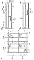
図2(a)は、画素アレイ110のうち第4〜第5行かつ第3列〜第4列の部分の上面レイアウトを示す模式図である。図中において、第5行かつ第3列には、画素PX_B及びユニットUMが配され、それ以外の位置には画素PX_Aが配されている。図2(b)は、図2(a)におけるカットラインX1−X2の断面構造を示す模式図である。図2(c)は、図2(a)におけるカットラインY1−Y2の断面構造を示す模式図である。
FIG. 2A is a schematic diagram illustrating an upper surface layout of a portion of the
図2(a)によると、画素PXが配列された基板上面に対する平面視(以下、単に「平面視」という。)において、画素PX_AのトランジスタW_Aは、センサS_Aと、そのコーナー部において重なるように配されている。例えば、第4行かつ第3列の画素PX_Aを参照すると、ゲート線G4は、トランジスタW_Aと近接するように行方向に沿って配され、信号線LC3は、トランジスタW_Aと近接するように列方向に沿って配されている。他の画素PX_Aについても同様である。 According to FIG. 2A, the transistor W_A of the pixel PX_A overlaps with the sensor S_A at a corner thereof in a plan view (hereinafter, simply referred to as “plan view”) with respect to the upper surface of the substrate on which the pixels PX are arranged. Are arranged. For example, referring to the pixels PX_A in the fourth row and third column, the gate line G4 is arranged along the row direction so as to be close to the transistor W_A, and the signal line LC3 is arranged in the column direction so as to be close to the transistor W_A. It is arranged along. The same applies to the other pixels PX_A.
第5行かつ第3列において、画素PX_Bは図中の上側に配され、ユニットUMは図中の下側に配されている。画素PX_Bは、平面視におけるセンサS_BのサイズがセンサS_Aよりも小さいことを除いて、画素PX_Aと同様に構成されうる。 In the fifth row and the third column, the pixel PX_B is arranged on the upper side in the figure, and the unit UM is arranged on the lower side in the figure. The pixel PX_B can be configured similarly to the pixel PX_A, except that the size of the sensor S_B in plan view is smaller than the sensor S_A.
ユニットUMは、第5行かつ第3列において画素PX_Bと共に配されており、本例では、平面視におけるセンサS_0のサイズがセンサS_Bと略等しく、画素PX_Bと実質的に点対称に配されている。これに伴い、ゲート線D5は、トランジスタW_Aと近接するように、ゲート線G5が配された側とは反対側においてゲート線G5と平行に(行方向に沿って)配されている。同様に、信号線J3は、トランジスタW_Aと近接するように、信号線LC3が配された側とは反対側において信号線LC3と平行に(列方向に沿って)配されている。 The unit UM is arranged along with the pixel PX_B in the fifth row and the third column. In this example, the size of the sensor S_0 in plan view is substantially equal to the sensor S_B, and is substantially point-symmetric with the pixel PX_B. I have. Accordingly, the gate line D5 is arranged in parallel with the gate line G5 (along the row direction) on the side opposite to the side where the gate line G5 is arranged so as to be close to the transistor W_A. Similarly, the signal line J3 is arranged in parallel with the signal line LC3 (along the column direction) on the side opposite to the side where the signal line LC3 is arranged so as to be close to the transistor W_A.
センサSに電力を供給するためのバイアス線VSは、各列に対応して列方向に沿って配されており、例えば第3列を参照すると、信号線LC3及び信号線J3との間に、これらと平行に(列方向に沿って)配されている。 The bias lines VS for supplying power to the sensors S are arranged in the column direction corresponding to each column. For example, referring to the third column, between the signal line LC3 and the signal line J3, They are arranged in parallel with these (along the column direction).
画素PX及びユニットUMは、例えば、ガラス等の絶縁部材で構成された基板210上に、上述の各要素を形成する部材が配されて成る。例えば、図2(b)を参照すると(ここでは説明を省略するが、図2(c)についても同様である。)、基板210上に、トランジスタW_0のゲートに対応する電極D5が配されており、基板210及び電極D5を覆うように絶縁膜220が配されている。電極D5の上には、トランジスタW_0のチャネルを形成する半導体部材が絶縁膜220を介して配されている。該半導体部材の両端には、それぞれドレインおよびソースに対応する電極が配されている。
Each of the pixels PX and the unit UM includes, for example, members forming the above-described elements disposed on a
上記ドレインに対応する電極は、信号線J3と一体に形成され得、換言すると、信号線J3は、該ドレインに対応する電極としてトランジスタW_0側まで延在している。一方、上記ソースに対応する電極は、トランジスタW_0や信号線LC3が配された基板210の上に保護膜230および層間絶縁膜240を介して配されたセンサS_0に、接続される。具体的には、センサS_0は、PIN接合を形成する半導体部250、並びに、その下面側および上面側にそれぞれ配された下側電極260及び上側電極261を含み得、ソースに対応する電極は、コンタクトホールを介して下側電極260と接触している。
The electrode corresponding to the drain can be formed integrally with the signal line J3. In other words, the signal line J3 extends to the transistor W_0 side as the electrode corresponding to the drain. On the other hand, the electrode corresponding to the source is connected to a sensor S_0 arranged via a
また、センサS_0の上には、保護膜231及び層間絶縁膜241を介してバイアス線VSが配されており、バイアス線VSは、コンタクトホールを介して上側電極261と接触している。更に、層間絶縁膜241およびバイアス線VSを覆うように保護膜232が配されている。
On the sensor S_0, a bias line VS is provided via a
以下、図3〜4を参照しながら、上記放射線撮像装置100の駆動方法ないし制御方法であって特に実施形態に係る自動露出制御(AEC)の方法の一例を説明する。
Hereinafter, an example of a method for driving or controlling the
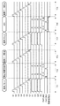
図3は、本方法を説明するためのフローチャートの例である。図4は、本方法に対応するタイミングチャートの例である。図4において、横軸は時間軸に対応し、縦軸には、ゲート線G1〜G7及びD1〜D4の電位、その他の信号(CNT_SH2及びCNT_RS2)、並びに、放射線強度を示している。 FIG. 3 is an example of a flowchart for explaining the present method. FIG. 4 is an example of a timing chart corresponding to the present method. 4, the horizontal axis corresponds to the time axis, and the vertical axis indicates the potentials of the gate lines G1 to G7 and D1 to D4, other signals (CNT_SH2 and CNT_RS2), and the radiation intensity.
ゲート線G1〜G7及びD1〜D4は、ハイレベル(Hレベル)のとき、対応するトランジスタWが導通状態になり、ローレベル(Lレベル)のとき、対応するトランジスタWが非導通状態になることを示す。信号CNT_SH2は、図1を参照しながら述べたサンプリング部SH2の制御信号であり、信号CNT_SH2がHレベルとなったとき、そのときの信号線J2等の信号がサンプリングされることを示す。信号CNT_RS2は、信号線J2〜J3及びJ5〜J6の電位をリセット(初期化)するための制御信号であり、信号CNT_RS2がHレベルとなったとき、信号線J2等の電位がリセットされることを示す。放射線強度は、単位時間あたりの放射線の照射量に相当し、Lレベルの場合には放射線が照射されていないことを示し、また、Hレベルの場合には放射線が照射されていることを示す。ここでは説明の容易化のため、これらのいずれについても理想的な矩形形状の波形で示す。 When the gate lines G1 to G7 and D1 to D4 are at the high level (H level), the corresponding transistor W is turned on, and when the gate lines G1 to G7 are at the low level (L level), the corresponding transistor W is turned off. Is shown. The signal CNT_SH2 is a control signal of the sampling unit SH2 described with reference to FIG. 1, and indicates that when the signal CNT_SH2 goes to the H level, the signal of the signal line J2 and the like at that time is sampled. The signal CNT_RS2 is a control signal for resetting (initializing) the potentials of the signal lines J2 to J3 and J5 to J6. When the signal CNT_RS2 becomes H level, the potential of the signal line J2 and the like is reset. Is shown. The radiation intensity is equivalent to the radiation dose per unit time. When the radiation intensity is at the L level, it indicates that the radiation has not been irradiated, and when the radiation level is at the H level, it indicates that the radiation has been irradiated. Here, for simplicity of explanation, all of these are shown by ideal rectangular waveforms.
ステップS100(以下、単に「S100」と表現する。他のステップについても同様である。)では、撮影準備を行う。具体的には、放射線撮像装置100に電力が供給されてから各ユニットが放射線撮影を行うことが可能な状態になるまで待機し、その後、放射線撮影に必要な初期設定(パラメータの設定等)を各ユニットに対して行う。
In step S100 (hereinafter, simply referred to as "S100". The same applies to other steps), preparation for photographing is performed. Specifically, after power is supplied to the
S110では、後述のAECを適切に行うための補正用信号を取得する。S110は、図4に示された期間T41に対応し、放射線の照射の開始前に(放射線が照射されていない状態で)為される。 In S110, a correction signal for appropriately performing AEC described later is acquired. S110 corresponds to the period T41 shown in FIG. 4 and is performed before radiation irradiation is started (in a state where radiation is not being irradiated).
S110は、例えば、信号CNT_RS2、CNT_SH2、D1〜D4、CNT_SH2の順にHレベルのパルスを供給する一連の動作OP1を繰り返すことによって為されうる。なお、「Hレベルのパルスを供給する」とは、Lレベルから、所定期間にわたってHレベルに維持した後にLレベルに戻すことを示し、以下では説明を容易にするため単に「Hレベルにする」と表現する場合がある。 S110 can be performed, for example, by repeating a series of operations OP1 for supplying H-level pulses in the order of the signals CNT_RS2, CNT_SH2, D1 to D4, and CNT_SH2. Note that "supplying an H-level pulse" indicates that the L-level is maintained at the H-level for a predetermined period and then returned to the L-level. May be expressed as
1回の動作OP1では、まず、信号CNT_RS2をHレベルにして信号線J2等をリセットした後、信号CNT_SH2をHレベルにして該リセットされた信号線J2等の信号をサンプリングすることによって第1信号が得られる。次に、ゲート線D1等をHレベルにしてセンサSの信号を信号線J2等に伝搬させ、これにより電位変動した信号線J2等の信号を、信号CNT_SH2をHレベルにしてサンプリングすることによって第2信号が得られる。 In one operation OP1, first, the signal CNT_RS2 is set to the H level to reset the signal line J2 and the like, and then the signal CNT_SH2 is set to the H level to sample the signal of the reset signal line J2 and the like. Is obtained. Next, the signal of the sensor S is propagated to the signal line J2 and the like by setting the gate line D1 and the like to the H level, and the signal of the signal line J2 and the like whose potential is fluctuated is sampled by setting the signal CNT_SH2 to the H level. Two signals are obtained.
本明細書において、上記第1信号を信号SIG1と表現し、上記第2信号を信号SIG2と表現する。即ち、信号SIG1は、トランジスタW_0が非導通状態(ゲート線D1等がLレベルである状態)での信号線J2等の信号に対応する。また、信号SIG2は、トランジスタW_0が導通状態(ゲート線D1等をHレベルである状態)での信号線J2等の信号に対応する。例えば、トランジスタW_0を導通状態にする前とトランジスタW_0を導通状態にした後とでは、信号線J2等の信号(電圧)が変わる可能性があり、信号SIG1の信号値と信号SIG2の信号値とは互いに異なりうる。このことは、例えば、トランジスタW_0に電荷がトラップされたこと等に起因すると考えられる。 In this specification, the first signal is expressed as a signal SIG1, and the second signal is expressed as a signal SIG2. That is, the signal SIG1 corresponds to the signal on the signal line J2 and the like in a state where the transistor W_0 is off (the state where the gate line D1 and the like are at the L level). The signal SIG2 corresponds to a signal on the signal line J2 or the like when the transistor W_0 is in a conductive state (a state in which the gate line D1 and the like are at the H level). For example, before the transistor W_0 is turned on and after the transistor W_0 is turned on, the signal (voltage) of the signal line J2 and the like may change, and the signal value of the signal SIG1 and the signal value of the signal SIG2 may be different. Can be different from each other. This is considered to be due to, for example, trapping of electric charge in the transistor W_0.
補正用信号SIG1及びSIG2は、上記繰り返し為された動作OP1により得られた複数の結果に基づいて(具体的には、それらの平均値、中央値、標準偏差等に基づいて)算出されてもよい。ここでは動作OP1を繰り返し行う(複数回の動作OP1を行う)態様を例示したが、動作OP1を1回のみ行い、信号SIG1及びSIG2は、該1回の動作OP1により得られた結果に基づいて算出されてもよい。 The correction signals SIG1 and SIG2 may be calculated based on a plurality of results obtained by the repeated operation OP1 (specifically, based on their average value, median value, standard deviation, and the like). Good. Here, the mode in which the operation OP1 is repeatedly performed (the operation OP1 is performed a plurality of times) is illustrated, but the operation OP1 is performed only once, and the signals SIG1 and SIG2 are based on the result obtained by the one operation OP1. It may be calculated.
S120では、撮影開始許可を示す信号を出力し、これに応じてユーザは、放射線の照射の開始を決定することができる。これと共に、図4に示された期間T42に対応する画素リセットを行ってもよい。具体的には、ゲート線G1〜G7を順にHレベルにする。この動作は、初期化動作(リセット動作)に対応し、これにより、各画素PXにおいて生じうるノイズ成分(暗電流等に起因するノイズ成分)を除去することができる。この間、ゲート線D1〜D4をHレベルに維持することによってユニットUMがアクティブ状態に維持されるため、ユニットUMからの信号に基づいて、放射線の照射が開始されたことを検知することも可能である。 In S120, a signal indicating permission to start imaging is output, and in response to this, the user can determine the start of radiation irradiation. At the same time, a pixel reset corresponding to the period T42 shown in FIG. 4 may be performed. Specifically, the gate lines G1 to G7 are sequentially set to the H level. This operation corresponds to an initialization operation (reset operation), whereby a noise component (a noise component caused by a dark current or the like) that can occur in each pixel PX can be removed. During this time, since the unit UM is maintained in the active state by maintaining the gate lines D1 to D4 at the H level, it is also possible to detect the start of radiation irradiation based on a signal from the unit UM. is there.
S130では、S110で補正用信号SIG1及びSIG2を取得してから装置100内の環境に変化があったか判断する。ここで、環境とは、例えば、装置100内の温度、電磁波等のノイズ量、装置100への圧力(例えば気圧、押圧)等を含み得、装置100はこれらの少なくとも一つを検知するための他のセンサ(不図示)をさらに備えてもよい。装置100内の環境が変化した場合にはS135に進み、そうでない場合にはS140に進む。
In S130, it is determined whether the environment in the
S135では、補正用信号SIG1及びSIG2の更新がS110と同様の手順で為されうる。即ち、S135では、上記変化した環境に対応する補正用信号SIG1及びSIG2を新たに取得する。S135では、上述の画素リセット(期間T42参照)は中断され得、補正用信号SIG1及びSIG2の更新が終了した後に再開されればよい。 In S135, the correction signals SIG1 and SIG2 can be updated in the same procedure as in S110. That is, in S135, the correction signals SIG1 and SIG2 corresponding to the changed environment are newly acquired. In S135, the above-described pixel reset (see the period T42) may be interrupted, and may be restarted after the update of the correction signals SIG1 and SIG2 is completed.
S140では、放射線の照射が開始されたか判断する。放射線の照射が開始されていない場合にはS130に戻り、該照射が開始された場合にはS150に進む。S140は、例えば、前述のとおり、ユニットUMからの信号に基づいて為されてもよいが、バイアス線VSの電流量の変化に基づいて為されてもよいし、別途用意された専用の検知部に基づいて為されてもよい。 In S140, it is determined whether irradiation of radiation has started. If the irradiation has not been started, the process returns to S130. If the irradiation has started, the process proceeds to S150. S140 may be performed based on a signal from the unit UM, for example, as described above, may be performed based on a change in the amount of current of the bias line VS, or may be a separately provided dedicated detection unit. May be performed based on
S150では、AEC用信号のモニタを行う。S150は、図4に示された期間T43に対応する。S150は、期間T41の動作と同様の手順で為されればよく、即ち、信号CNT_RS2、CNT_SH2、D1〜D4、CNT_SH2の順にHレベルにする一連の動作OP1を繰り返すことによって為されうる。1回の動作OP1では、まず、ゲート線D1等がLレベルである状態で信号CNT_RS2をHレベルにした後(信号線J2等をリセットした後)の信号線J2等の信号をサンプリングすることによって第3信号が得られる。次に、ゲート線D1等をHレベルである状態(センサSの信号を信号線J2等に伝搬させた後)の信号線J2等の信号をサンプリングすることによって第4信号が得られる。本明細書において、上記第3信号を信号SIG3と表現し、上記第4信号を信号SIG4と表現する。即ち、S150では、動作OP1を所定の周期で繰り返すことにより、AEC用信号SIG3及びSIG4を該所定の周期で読み出し、モニタする。 In S150, an AEC signal is monitored. S150 corresponds to the period T43 shown in FIG. S150 may be performed by the same procedure as the operation in the period T41, that is, by repeating a series of operations OP1 in which the signals CNT_RS2, CNT_SH2, D1 to D4, and CNT_SH2 are sequentially set to the H level. In one operation OP1, first, the signal on the signal line J2 or the like after the signal CNT_RS2 is set to the H level (after the signal line J2 or the like is reset) while the gate line D1 or the like is at the L level is sampled. A third signal is obtained. Next, a fourth signal is obtained by sampling the signal of the signal line J2 and the like in the state where the gate line D1 and the like are at the H level (after the signal of the sensor S is propagated to the signal line J2 and the like). In this specification, the third signal is expressed as a signal SIG3, and the fourth signal is expressed as a signal SIG4. That is, in S150, the operation OP1 is repeated at a predetermined cycle to read and monitor the AEC signals SIG3 and SIG4 at the predetermined cycle.
S160では、AEC用信号SIG3及びSIG4並びに補正用信号SIG1及びSIG2に基づいて、放射線の照射が開始されてからの照射量(放射線の強度の時間積分に相当する量)を算出する。具体的には、信号SIG3及びSIG4を信号SIG1及びSIG2により補正し、該補正された信号SIG3及びSIG4を累積加算する。このことを、以下、簡易的な式を参照しながら説明する。 In S160, the irradiation amount (the amount corresponding to the time integration of the radiation intensity) from the start of the radiation irradiation is calculated based on the AEC signals SIG3 and SIG4 and the correction signals SIG1 and SIG2. Specifically, the signals SIG3 and SIG4 are corrected by the signals SIG1 and SIG2, and the corrected signals SIG3 and SIG4 are cumulatively added. This will be described below with reference to simple equations.
S110および期間T41を参照しながら既に述べたとおり、トランジスタW_0が非導通状態とトランジスタW_0が導通状態とでは、信号線J2等の信号(電圧)が変わる可能性がある。そのため、補正用信号SIG1及びSIG2の信号値は、それぞれ、
SIG1=SS0a+SX1、
SIG2=SS0b+SX1
と示されうる。ここで、
SS0a:トランジスタW_0が非導通状態でのオフセット成分、
SS0b:トランジスタW_0が導通状態でのオフセット成分、
SX1:放射線照射前における他のノイズ成分
とする。
As described above with reference to S110 and the period T41, the signal (voltage) of the signal line J2 and the like may change between the non-conductive state of the transistor W_0 and the conductive state of the transistor W_0. Therefore, the signal values of the correction signals SIG1 and SIG2 are respectively
SIG1 = SS0a + SX1,
SIG2 = SS0b + SX1
Can be shown. here,
SS0a: offset component when transistor W_0 is off,
SS0b: Offset component when transistor W_0 is conductive,
SX1: Another noise component before irradiation.
同様に、放射線の照射後においても、トランジスタW_0が非導通状態とトランジスタW_0が導通状態とでは、信号線J2等の信号が変わる可能性がある。そのため、AEC用信号SIG3及びSIG4の信号値は、それぞれ、
SIG3=SS0a+SX2、
SIG4=SS0b+SX2+SA
と示されうる。ここで、
SX2:放射線照射中における他のノイズ成分、
SA:ユニットUMからの信号成分
とする。
Similarly, even after irradiation with radiation, a signal on the signal line J2 or the like may change depending on whether the transistor W_0 is off and the transistor W_0 is on. Therefore, the signal values of the AEC signals SIG3 and SIG4 are respectively
SIG3 = SS0a + SX2,
SIG4 = SS0b + SX2 + SA
Can be shown. here,
SX2: other noise components during irradiation,
SA: Signal component from unit UM.
ここで、単にAEC用信号SIG3及びSIG4の間の差分をとっても、SIG4−SIG3=SA+(SS0b−SS0a)となってしまい、信号成分SAそのものが適切に得られない。即ち、AECを行うのに際して、(SS0b−SS0a)に相当する誤差が生じうる。そこで、本実施形態では、(SIG4−SIG3)−(SIG2−SIG1)により、(SS0b−SS0a)に相当する成分を除去し、信号成分SAを適切に取得する。なお、ここでは2以上の信号の差分をとる方式を例示したが、それらの信号の読み出し方式を変えることにより、加算処理によって信号成分SAを取得してもよい。 Here, even if the difference between the AEC signals SIG3 and SIG4 is simply obtained, SIG4−SIG3 = SA + (SS0b−SS0a), and the signal component SA itself cannot be appropriately obtained. That is, when performing AEC, an error corresponding to (SS0b-SS0a) may occur. Therefore, in the present embodiment, the component corresponding to (SS0b-SS0a) is removed by (SIG4-SIG3)-(SIG2-SIG1), and the signal component SA is appropriately acquired. Here, a method of obtaining a difference between two or more signals has been described as an example, but the signal component SA may be obtained by an addition process by changing the reading method of those signals.
S160では、このようにして得られた信号成分SAを累積加算することにより、放射線の照射が開始されてからの照射量を算出する。S170では、S160の算出で得られた計算値(放射線の照射量)が基準値(放射線の照射量の設定値、許容値、上限値等)に達したか判断する。該計算値が基準値に達していない場合にはS150に戻り、達した場合にはS180に進む。S180では、放射線の照射の終了を要求する信号を出力し、放射線の照射を終了させる。 In S160, the irradiation amount after radiation irradiation is started is calculated by cumulatively adding the signal components SA thus obtained. In S170, it is determined whether or not the calculated value (radiation dose) obtained in the calculation in S160 has reached a reference value (a set value of radiation dose, an allowable value, an upper limit value, and the like). If the calculated value does not reach the reference value, the process returns to S150, and if it does, the process proceeds to S180. In S180, a signal requesting termination of radiation irradiation is output, and radiation irradiation is terminated.
放射線の照射の終了後、S190では、画像データの読み出しを行う。S190は、図4に示された期間T44に対応する。具体的には、ゲート線G1〜G7を順にHレベルにし、各画素PXから行単位で信号を順に読み出す。この動作は、読出動作に対応し、これにより画像データが生成され、この動作は、画像データ生成動作、画像データ取得動作等と称されてもよい。 After the end of the radiation irradiation, in S190, the image data is read. S190 corresponds to the period T44 shown in FIG. Specifically, the gate lines G1 to G7 are sequentially set to the H level, and signals are sequentially read from each pixel PX in row units. This operation corresponds to a read operation, whereby image data is generated, and this operation may be referred to as an image data generation operation, an image data acquisition operation, or the like.
ここで、前述のとおり、画素PX_Bは画素PX_Aより小サイズであるため、これらが互いに同じ線量の放射線を受けた場合でも、画素PX_Bからの信号の値は、画素PX_Aからの信号の値より小さくなりうる。そこで、画素PX_Bからの信号に対しては、これらのサイズ比(具体的には、平面視におけるセンサS_AとセンサS_Bとのサイズ比)に応じたゲインを用いて信号処理ないし補正処理が為されるとよい。別の観点では、画素PX_Bからの信号に対して用いられるゲインを、画素PX_Aからの信号に対して用いられうるゲインよりも大きくすればよい。 Here, as described above, since the pixel PX_B is smaller in size than the pixel PX_A, even when they receive the same dose of radiation, the value of the signal from the pixel PX_B is smaller than the value of the signal from the pixel PX_A. Can be. Therefore, the signal from the pixel PX_B is subjected to signal processing or correction processing using a gain corresponding to these size ratios (specifically, the size ratio between the sensor S_A and the sensor S_B in plan view). Good. From another viewpoint, the gain used for the signal from the pixel PX_B may be made larger than the gain that can be used for the signal from the pixel PX_A.
本実施形態によると、S150〜S180のステップは、AECの動作に相当し、S110及びS135のステップは、該AECの動作(特にS160での算出動作)を適切に行うための準備動作またはキャリブレーション動作に相当する。具体的には、放射線の照射開始前に、動作OP1により補正用信号SIG1及びSIG2を取得する。これら信号SIG1及びSIG2により、トランジスタW_0が非導通状態と導通状態とでのオフセット成分の差を算出することができる。その後、放射線の照射中では、動作OP1を繰り返し行うことによりAEC用信号SIG3及びSIG4をモニタし、信号SIG3及びSIG4を、信号SIG1及びSIG2で補正する。これにより、信号SIG3及びSIG4の間でのオフセット成分の差を除去することができ、該補正された信号SIG3及びSIG4に基づいて、適切にAECを行うことができる。よって、本実施形態によるとAECの高精度化に有利である。 According to the present embodiment, the steps S150 to S180 correspond to the operation of the AEC, and the steps S110 and S135 are the preparation operation or the calibration for appropriately performing the operation of the AEC (particularly the calculation operation in S160). Corresponds to an operation. Specifically, before the start of radiation irradiation, the correction signals SIG1 and SIG2 are obtained by operation OP1. From the signals SIG1 and SIG2, the difference between the offset components between the non-conductive state and the conductive state of the transistor W_0 can be calculated. Thereafter, during the irradiation of radiation, the operation OP1 is repeatedly performed to monitor the signals SIG3 and SIG4 for AEC, and correct the signals SIG3 and SIG4 with the signals SIG1 and SIG2. As a result, the difference between the offset components between the signals SIG3 and SIG4 can be removed, and AEC can be appropriately performed based on the corrected signals SIG3 and SIG4. Therefore, according to the present embodiment, it is advantageous to increase the accuracy of AEC.
(第2実施形態)
図5を参照しながら、第2実施形態を説明する。図5は、本実施形態に係るAECのタイミングチャートの例である。本実施形態は、補正用信号SIG1及びSIG2を取得する動作の前後の動作を、AECの動作の前後と同様にする、という点で第1実施形態(図4参照)と異なる。即ち、図5において、期間T51では画素リセットを行い、期間T52では補正用信号SIG1及びSIG2を取得し、期間T53では画像データの読み出しを行う。その後、放射線の照射が開始される前まで(期間T54で)、画素リセットを行い、期間T55でAECを行い、期間T56で画像データの読み出しを行う。期間T52、T54、T55、T56の動作は、それぞれ、図4を参照しながら述べた期間T41、T42、T43、T44の動作と同様である。
(2nd Embodiment)
The second embodiment will be described with reference to FIG. FIG. 5 is an example of an AEC timing chart according to the present embodiment. This embodiment is different from the first embodiment (see FIG. 4) in that the operations before and after the operation of acquiring the correction signals SIG1 and SIG2 are the same as before and after the operation of the AEC. That is, in FIG. 5, pixel reset is performed in a period T51, correction signals SIG1 and SIG2 are obtained in a period T52, and image data is read in a period T53. After that, until the start of radiation irradiation (period T54), pixel reset is performed, AEC is performed in period T55, and image data is read out in period T56. The operations in the periods T52, T54, T55, and T56 are the same as the operations in the periods T41, T42, T43, and T44 described with reference to FIG. 4, respectively.
本実施形態によると、補正用信号SIG1及びSIG2を取得するための期間T52の前の期間T51で画素リセットを行い、且つ、該期間T52の後の期間T53で画像データの読み出しを行う。そのため、期間T52での補正用信号SIG1及びSIG2を、期間T55でAEC用信号SIG3及びSIG4と同様の条件で取得することができる。これにより、信号SIG1のオフセット成分と信号SIG3のオフセット成分とがより近くなり得、また、信号SIG2のオフセット成分と信号SIG4のオフセット成分とがより近くなりうる。即ち、本実施形態によると、信号SIG3及びSIG4の間でのオフセット成分の差をより適切に除去することができる。よって、本実施形態によると、AECを更に高精度化することができる。 According to the present embodiment, pixel reset is performed in a period T51 before a period T52 for acquiring the correction signals SIG1 and SIG2, and image data is read in a period T53 after the period T52. Therefore, the correction signals SIG1 and SIG2 in the period T52 can be obtained under the same conditions as the AEC signals SIG3 and SIG4 in the period T55. Thus, the offset component of signal SIG1 and the offset component of signal SIG3 can be closer, and the offset component of signal SIG2 and the offset component of signal SIG4 can be closer. That is, according to the present embodiment, it is possible to more appropriately remove the difference between the offset components between the signals SIG3 and SIG4. Therefore, according to the present embodiment, the AEC can be further improved in accuracy.
なお、ここでは、期間T51の画素リセットおよび期間T53の画像データの読み出しの双方を行う態様を例示したが、補正用信号SIG1及びSIG2のオフセット成分に対する影響は、特に、期間T51の画素リセットに起因しうる。そのため、他の例では、期間T51の画素リセットを行う一方で、期間T53の画像データの読み出しを省略してもよい。 Here, the mode in which both the pixel reset in the period T51 and the reading of the image data in the period T53 are performed is illustrated, but the influence on the offset components of the correction signals SIG1 and SIG2 is particularly caused by the pixel reset in the period T51. Can. Therefore, in another example, the pixel data may be reset during the period T51, and the reading of the image data during the period T53 may be omitted.
(変形例)
図6(a)〜(b)を参照しながら変形例を説明する。
(Modification)
A modified example will be described with reference to FIGS.
図6(a)は、AECのタイミングチャートの第1の変形例である。第1の変形例では、期間T61で補正用信号SIG1及びSIG2が適切に取得されなかった場合に、その次の期間T62で、補正用信号SIG1及びSIG2を再取得する。信号SIG1及びSIG2が適切に取得されない場合として、例えば、それらの信号値が特異な値をとった場合(所定の範囲を超えている場合)が考えられる。信号SIG1及びSIG2が適切に得られたか否かの判断は、例えば、画素リセットを行っている間等に、制御部140等によって装置100の内部で為されればよい。
FIG. 6A is a first modified example of the AEC timing chart. In the first modification, when the correction signals SIG1 and SIG2 are not properly obtained in the period T61, the correction signals SIG1 and SIG2 are obtained again in the next period T62. As a case where the signals SIG1 and SIG2 are not appropriately acquired, for example, a case where their signal values take a peculiar value (a case where they exceed a predetermined range) can be considered. The determination as to whether or not the signals SIG1 and SIG2 are appropriately obtained may be made inside the
また、信号SIG1及びSIG2が適切に取得されない場合として、例えば、信号SIG1及びSIG2を取得している間に装置100の環境(前述のとおり、例えば温度等)が変化した場合等が考えられる。補正用信号SIG1及びSIG2の再取得が繰り返されるのを防ぐため、環境が安定したこと(例えば、温度等が定常状態になったこと、具体的には、温度等が所定の許容範囲内に収まったこと)に応じて、信号SIG1及びSIG2の取得が開始されてもよい。他の例では、環境が安定するのに十分な時間を予め取得しておいて、該時間が経過したことに応じて信号SIG1及びSIG2の取得が開始されてもよい。
Further, as a case where the signals SIG1 and SIG2 are not appropriately acquired, for example, a case where the environment (for example, temperature, etc., as described above) of the
期間T63、T64の動作は、それぞれ、図4を参照しながら述べた期間T43、T44の動作と同様である。 The operations in the periods T63 and T64 are the same as the operations in the periods T43 and T44 described with reference to FIG. 4, respectively.
図6(b)は、AECのタイミングチャートの第2の変形例である。例えば、放射線撮像装置100は、2つの動作モード(それぞれ第1モード、第2モードとする。)を含みうる。第2の変形例では、期間T71で第1モードについての補正用信号SIG1及びSIG2を取得し、期間T72で第2モードについての補正用信号SIG1及びSIG2を取得する。第1モードと第2モードとでは、例えば、制御信号の信号レベル(供給される電圧)が異なり、他の例では、読出部130でのゲイン等が異なり、さらに他の例では、画素PXが複数の感度を有するように構成されている場合には該感度が異なりうる。本例によると、各動作モードについての補正用信号SIG1及びSIG2を予め取得しておくことにより、いずれの動作モードで放射線撮影を行う場合でも、AECを適切に行うことができる。
FIG. 6B is a second modified example of the AEC timing chart. For example, the
ここでは駆動方法ないし制御方法の変形例を主に述べたが、構成面においても多様な変形例が考えられうる。例えば、画素アレイ110の構成(より具体的には、画素PX_A及びPX_B並びにユニットUMのそれぞれの構成)は、図1〜2に示された例に限られるものではなく、本発明の趣旨を逸脱しない範囲で、それらの一部が変更されてもよい。例えば、本実施形態では、ユニットUMの信号と画素PXの信号とを異なる信号線を用いて読み出す構成を例示したが、これらは共通の信号線により読み出されてもよい(即ち、信号線LC2等はユニットUMにより共有されてもよい。)。この構成によっても、トランジスタW_0が導通状態のときのセンサの信号と非導通状態のときのセンサの信号とが、これらの差が得られるように出力されうる。 Here, modifications of the driving method or the control method have been mainly described, but various modifications can be considered also in terms of configuration. For example, the configuration of the pixel array 110 (more specifically, the configuration of each of the pixels PX_A and PX_B and the unit UM) is not limited to the examples illustrated in FIGS. Some of them may be changed to the extent that they do not. For example, in the present embodiment, the configuration in which the signal of the unit UM and the signal of the pixel PX are read using different signal lines has been described, but these may be read by a common signal line (that is, the signal line LC2). Etc. may be shared by the unit UM). With this configuration, a sensor signal when the transistor W_0 is in a conductive state and a sensor signal when the transistor W_0 is in a non-conductive state can be output so as to obtain a difference therebetween.
画素PX_B及びユニットUMの画素アレイ110における配置位置は、ユーザの関心領域に配されればよく、或いは、撮影対象とする部位が決まっている場合には該部位に基づいて決定されてもよい。典型的には、画素PX_B及びユニットUMは、画素アレイ110の周辺領域ないしコーナー領域に配されうる。また、本例では、これらが列方向に2つずつ配された構成を示したが、これらの配置の数は、1つずつでもよいし、3以上連続して配されてもよいし、更に、これらは行方向(又は行方向および列方向の双方)に配されてもよい。
The arrangement positions of the pixels PX_B and the unit UM in the
また、本実施形態では、ユニットUMが画素PX_Bと共に1行×1列の単位を形成するように配された構成を例示したが、ユニットUMは、それ単体で1行×1列の単位を形成するように配されてもよい。この場合、この位置に相当する画素信号は、隣接画素PXの信号により補完されればよい。他の例では、ユニットUMは、画素アレイ110の外に配されてもよい。
Further, in the present embodiment, the configuration in which the unit UM is arranged so as to form a unit of 1 row × 1 column together with the pixel PX_B is exemplified, but the unit UM alone forms a unit of 1 row × 1 column. It may be arranged so that. In this case, the pixel signal corresponding to this position may be complemented by the signal of the adjacent pixel PX. In another example, the unit UM may be provided outside the
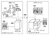
(放射線撮像システムへの適用例)
図7に例示されるように、上述の各実施形態で述べた放射線撮像装置は、放射線検査装置等に代表される撮像システムに適用されうる。放射線は、X線、α線、β線、γ線等を含む。ここでは、代表例としてX線を用いる場合を述べる。
(Example of application to radiation imaging system)
As illustrated in FIG. 7, the radiation imaging apparatus described in each of the above embodiments can be applied to an imaging system represented by a radiation inspection apparatus or the like. Radiation includes X-rays, α-rays, β-rays, γ-rays, and the like. Here, a case where X-rays are used as a representative example will be described.
X線チューブ610(放射線源)で発生したX線611は、被検者620の胸部621を透過し、放射線撮像装置630に入射する。該入射したX線611には患者620の体内の情報が含まれており、装置630により該X線611に応じた電気的情報が得られる。この電気的情報は、ディジタル信号に変換された後、例えばイメージプロセッサ640(信号処理部)によって所定の信号処理が為される。医師等のユーザは、該電気的情報に応じた放射線画像を、例えばコントロールルームのディスプレイ650(表示部)で観察することができる。ユーザは、放射線画像又はそのデータを、所定の通信手段660により遠隔地へ転送することができ、該放射線画像を、例えばドクタールーム等の他の場所のディスプレイ651で観察することもできる。また、ユーザは、該放射線画像又はそのデータを所定の記録媒体に記録することもでき、例えば、フィルムプロセッサ670によってフィルム671に記録することができる。
The
(その他)
本発明は、上述の実施形態の1以上の機能を実現するプログラムをネットワーク又は記憶媒体を介してシステム又は装置に供給し、該システム又は装置のコンピュータにおける1以上のプロセッサがプログラムを読み出して実行する処理により実現されてもよい。例えば、本発明は、1以上の機能を実現する回路(例えば、ASIC)によって実現されてもよい。
(Other)
The present invention supplies a program for realizing one or more functions of the above-described embodiments to a system or an apparatus via a network or a storage medium, and one or more processors in a computer of the system or the apparatus read and execute the program. It may be realized by processing. For example, the present invention may be realized by a circuit (for example, an ASIC) that realizes one or more functions.
以上、本発明に係るいくつかの好適な態様を例示したが、本発明はこれらの例に限られるものではなく、本発明の趣旨を逸脱しない範囲で、その一部が変更されてもよい。例えば、上述の実施形態では、放射線を検知するのに、放射線を光に変換して該光を光電変換する構成(いわゆる間接変換型)を例示したが、放射線を直接的に電気信号に変換する構成(いわゆる直接変換型)が採られてもよい。 The preferred embodiments according to the present invention have been described above, but the present invention is not limited to these embodiments, and some of them may be modified without departing from the spirit of the present invention. For example, in the above-described embodiment, in order to detect radiation, a configuration in which radiation is converted to light and the light is photoelectrically converted (a so-called indirect conversion type) is illustrated, but the radiation is directly converted to an electric signal. A configuration (so-called direct conversion type) may be adopted.
また、本明細書に記載された個々の用語は、本発明を説明する目的で用いられたものに過ぎず、本発明は、その用語の厳密な意味に限定されるものでないことは言うまでもなく、その均等物をも含みうる。 Further, individual terms described in this specification are merely used for describing the present invention, and it is needless to say that the present invention is not limited to the strict meaning of the terms. It may also include its equivalents.
100:放射線撮像装置、PX:画素、UM:AEC用ユニット、S:検知素子、W:スイッチ素子、140:制御部。 100: radiation imaging apparatus, PX: pixel, UM: AEC unit, S: detection element, W: switch element, 140: control unit.
Claims (17)
前記画素とは異なるユニットであって、放射線を検知するための検知素子と、前記検知素子に対応するスイッチ素子と、を含むユニットと、
前記スイッチ素子が導通状態になったことに応じて前記検知素子から出力された信号を伝搬する信号線と、
制御部と、を備える放射線撮像装置であって、
前記制御部は、
前記放射線撮像装置に対する放射線の照射の開始前において、前記信号線の電位をリセットしてから前記スイッチ素子を導通状態にするまでの間の前記信号線の信号を第1信号として取得し、該スイッチ素子を導通状態にしてから前記信号線の電位をリセットするまでの間の前記信号線の信号を第2信号として取得する第1動作と、
前記放射線の照射が開始されたことに応答して、前記信号線の電位をリセットしてから前記スイッチ素子を導通状態にするまでの間の前記信号線の信号を第3信号として取得し、該スイッチ素子を導通状態にしてから前記信号線の電位をリセットするまでの間の前記信号線の信号を第4信号としてモニタする第2動作と、
前記第1信号、前記第2信号、前記第3信号及び前記第4信号に基づいて、前記放射線の照射が開始されてからの前記放射線の照射量を算出する第3動作と、
を行う
ことを特徴とする放射線撮像装置。 A plurality of pixels,
A unit different from the pixel, a detection element for detecting radiation, and a unit including a switch element corresponding to the detection element ,
A signal line for transmitting a signal output from the detection element in response to the switching element being turned on ,
And a control unit , comprising:
The control unit includes:
Before starting irradiation of radiation to the radiation imaging apparatus, a signal on the signal line from resetting the potential of the signal line to turning on the switch element is obtained as a first signal, and the switch first operation and for obtaining a potential of the signal line from the device to the conductive state signal of the signal line between a reset until a second signal,
In response to the start of irradiation of the radiation, a signal on the signal line from resetting the potential of the signal line to turning on the switch element is acquired as a third signal, and a second operation for monitoring the fourth signal a signal of the signal line during the period from the switching element to a conducting state in the reset until the potential of the signal line,
A third operation of calculating an irradiation amount of the radiation from the start of the irradiation of the radiation based on the first signal, the second signal, the third signal, and the fourth signal ;
A radiation imaging apparatus characterized by performing:
ことを特徴とする請求項1に記載の放射線撮像装置。 In the third operation, the control unit may include a first difference that is a difference between the first signal and the second signal, and a second difference that is a difference between the third signal and the fourth signal. The radiation imaging apparatus according to claim 1, wherein the radiation irradiation amount is calculated based on:
ことを特徴とする請求項2に記載の放射線撮像装置。 The radiation imaging apparatus according to claim 2, wherein the control unit calculates the radiation dose based on a difference between the first difference and the second difference in the third operation. .
前記第1動作の後かつ前記第2動作の前に、前記複数の画素のそれぞれを初期化する第1初期化動作と、
前記第1動作の前に、前記複数の画素のそれぞれを初期化する第2初期化動作と、
算出された前記照射量が基準値に達したことに応じて出力された信号に応じて前記放射線の照射が終了された後に前記複数の画素から画像データを読み出す第4の動作と、
をさらに行う
ことを特徴とする請求項1から請求項3のいずれか1項に記載の放射線撮像装置。 The control unit includes:
A first initialization operation for initializing each of the plurality of pixels after the first operation and before the second operation;
A second initialization operation for initializing each of the plurality of pixels before the first operation;
A fourth operation of reading image data from the plurality of pixels after the irradiation of the radiation is terminated in accordance with a signal output in response to the calculated irradiation amount reaching a reference value,
The radiation imaging apparatus according to any one of claims 1 to 3, further comprising:
前記制御部は、前記第1動作の後かつ前記第1初期化動作の前に、前記複数の画素から画像データを読み出す第2読出動作をさらに行う
ことを特徴とする請求項4に記載の放射線撮像装置。 The operation of reading the image data is a first reading operation,
The radiation according to claim 4, wherein the control unit further performs a second read operation of reading image data from the plurality of pixels after the first operation and before the first initialization operation. Imaging device.
ことを特徴とする請求項1から請求項5のいずれか1項に記載の放射線撮像装置。 The control unit is configured to control the signal line when at least one of a temperature in the radiation imaging apparatus, a noise amount in the radiation imaging apparatus, and a pressure on the radiation imaging apparatus changes before the start of the radiation irradiation. The signal of the signal line between the time when the potential of the switch element is reset and the time when the switch element is turned on is obtained as a new first signal, and the potential of the signal line is reset after the switch element is turned on. The signal of the said signal line until it performs is acquired as a new 2nd signal. The radiation imaging device of any one of Claim 1 to 5 characterized by the above-mentioned.
ことを特徴とする請求項6に記載の放射線撮像装置。 7. The radiation imaging apparatus according to claim 6, wherein in the first operation, the control unit acquires the first signal and the second signal in response to the at least one being in a steady state. 8. apparatus.
前記制御部は、前記第1動作では、前記複数のモードのそれぞれについて前記第1信号および前記第2信号を取得する
ことを特徴とする請求項1から請求項7のいずれか1項に記載の放射線撮像装置。 It has multiple modes as operation modes,
The said control part acquires the said 1st signal and the said 2nd signal about each of these modes in the said 1st operation | movement. The method of any one of Claim 1 to 7 characterized by the above-mentioned. Radiation imaging device.
前記複数の画素は、複数の行および複数の列を形成するように配列されており、
前記第1画素は、1行かつ1列の単位に対応し、前記検知素子と前記スイッチ素子と前記第2画素とは、1行かつ1列の単位に対応する
ことを特徴とする請求項1から請求項8のいずれか1項に記載の放射線撮像装置。 The plurality of pixels include a first pixel and a second pixel smaller in size than the first pixel,
The plurality of pixels are arranged to form a plurality of rows and a plurality of columns,
The first pixel corresponds to a unit of one row and one column, and the sensing element, the switch element, and the second pixel correspond to a unit of one row and one column. The radiation imaging apparatus according to any one of claims 1 to 8.
ことを特徴とする請求項9に記載の放射線撮像装置。 The radiation imaging apparatus according to claim 9, wherein the signal line is arranged along a column in which the second pixels are arranged.
前記第2画素が配された列に対応する列信号線と、前記信号線とは互いに平行に配されている
ことを特徴とする請求項9または請求項10に記載の放射線撮像装置。 A plurality of column signal lines corresponding to the plurality of columns, further comprising a plurality of column signal lines for reading a pixel signal from each pixel of the corresponding column,
11. The radiation imaging apparatus according to claim 9, wherein a column signal line corresponding to a column in which the second pixels are arranged, and the signal line are arranged in parallel with each other. 12.
ことを特徴とする請求項9から請求項11のいずれか1項に記載の放射線撮像装置。 In the operation of reading image data from the plurality of pixels, the control unit may use a gain corresponding to a size ratio between the first pixel and the second pixel to a signal read from the second pixel. The radiation imaging apparatus according to any one of claims 9 to 11, which performs processing.
前記電力供給線は、前記複数の画素が配列された基板の上面に対する平面視において、
前記第2画素が配された列に対応する列信号線と、前記信号線との間に、それらと平行に配されている
ことを特徴とする請求項9から請求項12のいずれか1項に記載の放射線撮像装置。 Further comprising a power supply line for supplying power to each of the plurality of pixels,
The power supply line is a plan view with respect to an upper surface of the substrate on which the plurality of pixels are arranged.
13. A column signal line corresponding to a column in which the second pixels are arranged, and the signal line, arranged in parallel with the signal lines. A radiation imaging apparatus according to claim 1.
前記第1信号及び前記第2信号は、繰り返し為された前記第1動作により得られた複数の結果に基づいて算出されるThe first signal and the second signal are calculated based on a plurality of results obtained by the repeated first operation.
ことを特徴とする請求項1から請求項13のいずれか1項に記載の放射線撮像装置。The radiation imaging apparatus according to any one of claims 1 to 13, wherein:
ことを特徴とする請求項14に記載の放射線撮像装置。The radiation imaging apparatus according to claim 14, wherein:
前記放射線撮像装置からの信号を処理するプロセッサと、を具備する
ことを特徴とする放射線撮像システム。 A radiation imaging apparatus according to any one of claims 1 to 15 ,
A processor for processing a signal from the radiation imaging apparatus.
前記画素とは異なるユニットであって、放射線を検知するための検知素子と、前記検知素子に対応するスイッチ素子と、を含むユニットと、
前記スイッチ素子が導通状態になったことに応じて前記検知素子から出力された信号を伝搬する信号線と、を備える放射線撮像装置の駆動方法であって、
前記放射線撮像装置に対する放射線の照射の開始前において、前記信号線の電位をリセットしてから前記スイッチ素子を導通状態にするまでの間、および該スイッチ素子を導通状態にしてから前記信号線の電位をリセットするまでの間の前記信号線の信号を、それぞれ第1信号および第2信号として取得する工程と、
前記放射線の照射が開始されたことに応答して、前記信号線の電位をリセットしてから前記スイッチ素子を導通状態にするまでの間、および該スイッチ素子を導通状態にしてから前記信号線の電位をリセットするまでの間の前記信号線の信号を、それぞれ第3信号および第4信号としてモニタする工程と、
前記第1信号、前記第2信号、前記第3信号及び前記第4信号に基づいて、前記放射線の照射が開始されてからの前記放射線の照射量を算出する工程と、を含む
ことを特徴とする放射線撮像装置の駆動方法。
A plurality of pixels,
A unit that is different from the pixel and includes a detection element for detecting radiation and a switch element corresponding to the detection element .
A driving method of a radiation imaging apparatus and a signal line for propagating a signal output from said detecting element in response to the switching element becomes conductive,
Before the start of the irradiation of radiation on the radiation imaging apparatus, during the period from the reset potential of the signal line until the switch element in a conductive state, and the potential of the signal line after the switching element to a conducting state the signal of the signal line between the at reset until a step of acquiring a first signal and second signal, respectively,
In response to the start of the irradiation of the radiation, from resetting the potential of the signal line to turning on the switch element and from turning on the switch element to turning on the signal line. the signal of the signal line between the voltage at reset until the steps of monitoring the third signal and the fourth signal, respectively,
The first signal, the second signal, based on said third signal and said fourth signal, calculating a dose of the radiation from the start of irradiation of the radiation, and comprising a The driving method of the radiation imaging apparatus to be performed.
Priority Applications (2)
| Application Number | Priority Date | Filing Date | Title |
|---|---|---|---|
| JP2016004613A JP6649775B2 (en) | 2016-01-13 | 2016-01-13 | Radiation imaging apparatus, driving method thereof, and radiation imaging system |
| US15/366,048 US9838638B2 (en) | 2016-01-13 | 2016-12-01 | Radiation imaging apparatus, method of driving the same, and radiation imaging system |
Applications Claiming Priority (1)
| Application Number | Priority Date | Filing Date | Title |
|---|---|---|---|
| JP2016004613A JP6649775B2 (en) | 2016-01-13 | 2016-01-13 | Radiation imaging apparatus, driving method thereof, and radiation imaging system |
Publications (3)
| Publication Number | Publication Date |
|---|---|
| JP2017126860A JP2017126860A (en) | 2017-07-20 |
| JP2017126860A5 JP2017126860A5 (en) | 2019-02-28 |
| JP6649775B2 true JP6649775B2 (en) | 2020-02-19 |
Family
ID=59276395
Family Applications (1)
| Application Number | Title | Priority Date | Filing Date |
|---|---|---|---|
| JP2016004613A Active JP6649775B2 (en) | 2016-01-13 | 2016-01-13 | Radiation imaging apparatus, driving method thereof, and radiation imaging system |
Country Status (2)
| Country | Link |
|---|---|
| US (1) | US9838638B2 (en) |
| JP (1) | JP6649775B2 (en) |
Families Citing this family (17)
| Publication number | Priority date | Publication date | Assignee | Title |
|---|---|---|---|---|
| JP6570315B2 (en) | 2015-05-22 | 2019-09-04 | キヤノン株式会社 | Radiation imaging apparatus and radiation imaging system |
| JP6887812B2 (en) * | 2017-01-18 | 2021-06-16 | キヤノン株式会社 | Radiation imaging device and radiation imaging system |
| JP6929104B2 (en) | 2017-04-05 | 2021-09-01 | キヤノン株式会社 | Radiation imaging device, radiation imaging system, control method and program of radiation imaging device |
| JP6990986B2 (en) | 2017-04-27 | 2022-01-12 | キヤノン株式会社 | Radiation imaging device, radiation imaging system, control method and program of radiation imaging device |
| JP6853729B2 (en) | 2017-05-08 | 2021-03-31 | キヤノン株式会社 | Radiation imaging device, radiation imaging system, control method and program of radiation imaging device |
| JP6788547B2 (en) | 2017-05-09 | 2020-11-25 | キヤノン株式会社 | Radiation imaging device, its control method, control device, and radiation imaging system |
| WO2019012846A1 (en) | 2017-07-10 | 2019-01-17 | キヤノン株式会社 | Radiation imaging device and radiation imaging system |
| JP7045834B2 (en) | 2017-11-10 | 2022-04-01 | キヤノン株式会社 | Radiation imaging system |
| JP7079113B2 (en) | 2018-02-21 | 2022-06-01 | キヤノン株式会社 | Radiation imaging device and radiation imaging system |
| JP7198003B2 (en) | 2018-06-22 | 2022-12-28 | キヤノン株式会社 | Radiation Imaging Apparatus, Radiation Imaging System, Radiation Imaging Apparatus Control Method and Program |
| EP3661190A1 (en) | 2018-11-27 | 2020-06-03 | Canon Kabushiki Kaisha | Radiation imaging apparatus and radiation imaging system |
| JP7212530B2 (en) | 2019-01-24 | 2023-01-25 | キヤノン株式会社 | Radiation imaging system, control device and control method |
| JP7157699B2 (en) | 2019-05-29 | 2022-10-20 | キヤノン株式会社 | Radiation imaging apparatus, radiation imaging system, method for controlling radiation imaging apparatus, and program for executing the method |
| JP7410678B2 (en) | 2019-09-19 | 2024-01-10 | キヤノン株式会社 | Radiation imaging devices and radiation imaging systems |
| JP7397635B2 (en) | 2019-11-22 | 2023-12-13 | キヤノン株式会社 | Radiation detection device, radiation detection system, control method and program |
| JP2022022844A (en) | 2020-07-08 | 2022-02-07 | キヤノン株式会社 | Radiation imaging device |
| JP2022164433A (en) | 2021-04-16 | 2022-10-27 | キヤノン株式会社 | Radiation imaging apparatus and radiation imaging system |
Family Cites Families (29)
| Publication number | Priority date | Publication date | Assignee | Title |
|---|---|---|---|---|
| US6399950B1 (en) * | 2000-11-27 | 2002-06-04 | Shimadzu Corporation | Two-dimensional radiation detector |
| JP5058517B2 (en) | 2005-06-14 | 2012-10-24 | キヤノン株式会社 | Radiation imaging apparatus, control method therefor, and radiation imaging system |
| JP2007151761A (en) | 2005-12-02 | 2007-06-21 | Canon Inc | Apparatus, system, method, and program for radiation imaging |
| JP5196739B2 (en) | 2006-06-09 | 2013-05-15 | キヤノン株式会社 | Radiation imaging apparatus and radiation imaging system |
| JP2008042478A (en) | 2006-08-04 | 2008-02-21 | Canon Inc | Imaging device, radiation ray imaging device and its driving method |
| US7869568B2 (en) | 2007-03-13 | 2011-01-11 | Canon Kabushiki Kaisha | Radiation imaging apparatus, and method and program for controlling radiation imaging apparatus |
| JP4949908B2 (en) * | 2007-03-29 | 2012-06-13 | 富士フイルム株式会社 | Radiation image detection method and apparatus |
| JP5792923B2 (en) | 2009-04-20 | 2015-10-14 | キヤノン株式会社 | Radiation imaging apparatus, radiation imaging system, control method thereof, and program thereof |
| JP5517484B2 (en) | 2009-05-01 | 2014-06-11 | キヤノン株式会社 | Imaging apparatus and imaging system, control method thereof, and program thereof |
| EP2564779B1 (en) * | 2010-04-30 | 2017-08-30 | Konica Minolta Medical & Graphic, Inc. | Radiation image photography device |
| JP5653823B2 (en) * | 2010-06-30 | 2015-01-14 | 富士フイルム株式会社 | Radiation detection element and radiographic imaging device |
| JP5475574B2 (en) | 2010-07-02 | 2014-04-16 | 富士フイルム株式会社 | Radiation detection element and radiographic imaging device |
| JP5776693B2 (en) * | 2010-09-09 | 2015-09-09 | コニカミノルタ株式会社 | Radiographic imaging apparatus and radiographic imaging system |
| JP5764468B2 (en) * | 2010-11-26 | 2015-08-19 | 富士フイルム株式会社 | Radiographic image detection apparatus and radiographic imaging system |
| JP2012118312A (en) * | 2010-12-01 | 2012-06-21 | Fujifilm Corp | Radiation image detector and drive control method thereof |
| JP5847413B2 (en) * | 2011-03-24 | 2016-01-20 | キヤノン株式会社 | Imaging apparatus, imaging system, and control method thereof |
| US20140124678A1 (en) * | 2011-06-02 | 2014-05-08 | Konica Minolta, Inc. | Radiation imaging system |
| JP5866814B2 (en) * | 2011-06-20 | 2016-02-24 | コニカミノルタ株式会社 | Radiographic imaging system and radiographic imaging device |
| JP2014016343A (en) * | 2012-06-13 | 2014-01-30 | Canon Inc | Radiation image pickup apparatus, and method and program for radiation image pickup |
| JP2014003559A (en) * | 2012-06-21 | 2014-01-09 | Konica Minolta Inc | Radiation image pick-up device and radiation image pick-up system |
| JP6056380B2 (en) * | 2012-10-31 | 2017-01-11 | コニカミノルタ株式会社 | Radiation imaging system |
| JP6127718B2 (en) * | 2013-05-27 | 2017-05-17 | コニカミノルタ株式会社 | Radiographic imaging system and radiographic imaging device |
| JP6480670B2 (en) | 2014-05-01 | 2019-03-13 | キヤノン株式会社 | Radiation imaging apparatus and radiation imaging system |
| JP6585910B2 (en) | 2014-05-01 | 2019-10-02 | キヤノン株式会社 | Radiation imaging apparatus and radiation imaging system |
| JP6595803B2 (en) | 2014-06-13 | 2019-10-23 | キヤノン株式会社 | Radiation imaging apparatus, radiation imaging system and control method thereof |
| US9948871B2 (en) | 2014-07-25 | 2018-04-17 | Canon Kabushiki Kaisha | Radiation imaging apparatus and radiation imaging system |
| JP6491434B2 (en) | 2014-08-12 | 2019-03-27 | キヤノン株式会社 | Radiation imaging apparatus and radiation detection system |
| JP6413534B2 (en) * | 2014-09-17 | 2018-10-31 | コニカミノルタ株式会社 | Radiation imaging system |
| JP6626301B2 (en) | 2015-09-28 | 2019-12-25 | キヤノン株式会社 | Radiation imaging apparatus, radiation imaging system, control method of radiation imaging apparatus, and program |
-
2016
- 2016-01-13 JP JP2016004613A patent/JP6649775B2/en active Active
- 2016-12-01 US US15/366,048 patent/US9838638B2/en active Active
Also Published As
| Publication number | Publication date |
|---|---|
| US20170201704A1 (en) | 2017-07-13 |
| US9838638B2 (en) | 2017-12-05 |
| JP2017126860A (en) | 2017-07-20 |
Similar Documents
| Publication | Publication Date | Title |
|---|---|---|
| JP6649775B2 (en) | Radiation imaging apparatus, driving method thereof, and radiation imaging system | |
| JP6585910B2 (en) | Radiation imaging apparatus and radiation imaging system | |
| US9423513B2 (en) | Radiation imaging apparatus and radiation imaging system | |
| JP6339853B2 (en) | Radiation imaging apparatus and radiation imaging system | |
| JP4965931B2 (en) | Radiation imaging apparatus, radiation imaging system, control method thereof, and control program | |
| JP6555909B2 (en) | Radiation imaging apparatus and radiation imaging system | |
| JP6929104B2 (en) | Radiation imaging device, radiation imaging system, control method and program of radiation imaging device | |
| JP5539139B2 (en) | IMAGING DEVICE, IMAGING SYSTEM, AND IMAGING DEVICE CONTROL METHOD | |
| JP2018191152A (en) | Radiation imaging apparatus, radiation imaging system, control method for radiation imaging apparatus and program | |
| CN111214250B (en) | Radiation imaging apparatus and radiation imaging system | |
| JP2010005212A (en) | Radiographic imaging apparatus, control method thereof and radiographic imaging system | |
| US8446495B2 (en) | Image pickup apparatus and image pickup system | |
| JP4888599B2 (en) | Light or radiation imaging device | |
| US20200371259A1 (en) | Radiation imaging apparatus and radiation imaging system | |
| JP7373338B2 (en) | Radiation imaging device and radiation imaging system | |
| JP6525756B2 (en) | Radiation imaging apparatus and control method thereof | |
| JP2008141705A (en) | Radiation imaging apparatus and system | |
| JP6808458B2 (en) | Radiation imaging device and radiation imaging system | |
| JP2008154957A (en) | Image pickup device and its drive method | |
| JP7449260B2 (en) | Radiation imaging device and radiation imaging system | |
| JP7438720B2 (en) | Radiation imaging device and radiation imaging system | |
| JP7190360B2 (en) | Radiation imaging device and radiation imaging system | |
| JP6436754B2 (en) | Radiation imaging apparatus and radiation imaging system | |
| JP6555893B2 (en) | Radiation imaging apparatus and radiation imaging system | |
| JP2024004308A (en) | Radiation imaging device, radiation imaging system, method for controlling radiation imaging device, signal processing device, method for controlling signal processing device, and program |
Legal Events
| Date | Code | Title | Description |
|---|---|---|---|
| A521 | Request for written amendment filed |
Free format text: JAPANESE INTERMEDIATE CODE: A523 Effective date: 20190111 |
|
| A621 | Written request for application examination |
Free format text: JAPANESE INTERMEDIATE CODE: A621 Effective date: 20190111 |
|
| A977 | Report on retrieval |
Free format text: JAPANESE INTERMEDIATE CODE: A971007 Effective date: 20191115 |
|
| TRDD | Decision of grant or rejection written | ||
| A01 | Written decision to grant a patent or to grant a registration (utility model) |
Free format text: JAPANESE INTERMEDIATE CODE: A01 Effective date: 20191220 |
|
| A61 | First payment of annual fees (during grant procedure) |
Free format text: JAPANESE INTERMEDIATE CODE: A61 Effective date: 20200117 |
|
| R151 | Written notification of patent or utility model registration |
Ref document number: 6649775 Country of ref document: JP Free format text: JAPANESE INTERMEDIATE CODE: R151 |