JP6576306B2 - Voltage-current conversion circuit and load drive circuit - Google Patents
Voltage-current conversion circuit and load drive circuit Download PDFInfo
- Publication number
- JP6576306B2 JP6576306B2 JP2016127559A JP2016127559A JP6576306B2 JP 6576306 B2 JP6576306 B2 JP 6576306B2 JP 2016127559 A JP2016127559 A JP 2016127559A JP 2016127559 A JP2016127559 A JP 2016127559A JP 6576306 B2 JP6576306 B2 JP 6576306B2
- Authority
- JP
- Japan
- Prior art keywords
- transistor
- terminal
- voltage
- resistor
- current
- Prior art date
- Legal status (The legal status is an assumption and is not a legal conclusion. Google has not performed a legal analysis and makes no representation as to the accuracy of the status listed.)
- Active
Links
Images


Classifications
-
- G—PHYSICS
- G05—CONTROLLING; REGULATING
- G05F—SYSTEMS FOR REGULATING ELECTRIC OR MAGNETIC VARIABLES
- G05F1/00—Automatic systems in which deviations of an electric quantity from one or more predetermined values are detected at the output of the system and fed back to a device within the system to restore the detected quantity to its predetermined value or values, i.e. retroactive systems
- G05F1/10—Regulating voltage or current
- G05F1/46—Regulating voltage or current wherein the variable actually regulated by the final control device is dc
- G05F1/56—Regulating voltage or current wherein the variable actually regulated by the final control device is dc using semiconductor devices in series with the load as final control devices
- G05F1/561—Voltage to current converters
-
- G—PHYSICS
- G05—CONTROLLING; REGULATING
- G05F—SYSTEMS FOR REGULATING ELECTRIC OR MAGNETIC VARIABLES
- G05F3/00—Non-retroactive systems for regulating electric variables by using an uncontrolled element, or an uncontrolled combination of elements, such element or such combination having self-regulating properties
- G05F3/02—Regulating voltage or current
- G05F3/08—Regulating voltage or current wherein the variable is dc
- G05F3/10—Regulating voltage or current wherein the variable is dc using uncontrolled devices with non-linear characteristics
- G05F3/16—Regulating voltage or current wherein the variable is dc using uncontrolled devices with non-linear characteristics being semiconductor devices
- G05F3/20—Regulating voltage or current wherein the variable is dc using uncontrolled devices with non-linear characteristics being semiconductor devices using diode- transistor combinations
- G05F3/26—Current mirrors
-
- H—ELECTRICITY
- H03—ELECTRONIC CIRCUITRY
- H03K—PULSE TECHNIQUE
- H03K17/00—Electronic switching or gating, i.e. not by contact-making and –breaking
- H03K17/51—Electronic switching or gating, i.e. not by contact-making and –breaking characterised by the components used
- H03K17/56—Electronic switching or gating, i.e. not by contact-making and –breaking characterised by the components used by the use, as active elements, of semiconductor devices
- H03K17/687—Electronic switching or gating, i.e. not by contact-making and –breaking characterised by the components used by the use, as active elements, of semiconductor devices the devices being field-effect transistors
- H03K17/6871—Electronic switching or gating, i.e. not by contact-making and –breaking characterised by the components used by the use, as active elements, of semiconductor devices the devices being field-effect transistors the output circuit comprising more than one controlled field-effect transistor
- H03K17/6872—Electronic switching or gating, i.e. not by contact-making and –breaking characterised by the components used by the use, as active elements, of semiconductor devices the devices being field-effect transistors the output circuit comprising more than one controlled field-effect transistor using complementary field-effect transistors
-
- H—ELECTRICITY
- H05—ELECTRIC TECHNIQUES NOT OTHERWISE PROVIDED FOR
- H05B—ELECTRIC HEATING; ELECTRIC LIGHT SOURCES NOT OTHERWISE PROVIDED FOR; CIRCUIT ARRANGEMENTS FOR ELECTRIC LIGHT SOURCES, IN GENERAL
- H05B45/00—Circuit arrangements for operating light-emitting diodes [LED]
- H05B45/30—Driver circuits
- H05B45/37—Converter circuits
-
- H—ELECTRICITY
- H05—ELECTRIC TECHNIQUES NOT OTHERWISE PROVIDED FOR
- H05B—ELECTRIC HEATING; ELECTRIC LIGHT SOURCES NOT OTHERWISE PROVIDED FOR; CIRCUIT ARRANGEMENTS FOR ELECTRIC LIGHT SOURCES, IN GENERAL
- H05B45/00—Circuit arrangements for operating light-emitting diodes [LED]
- H05B45/30—Driver circuits
- H05B45/395—Linear regulators
- H05B45/397—Current mirror circuits
-
- Y—GENERAL TAGGING OF NEW TECHNOLOGICAL DEVELOPMENTS; GENERAL TAGGING OF CROSS-SECTIONAL TECHNOLOGIES SPANNING OVER SEVERAL SECTIONS OF THE IPC; TECHNICAL SUBJECTS COVERED BY FORMER USPC CROSS-REFERENCE ART COLLECTIONS [XRACs] AND DIGESTS
- Y02—TECHNOLOGIES OR APPLICATIONS FOR MITIGATION OR ADAPTATION AGAINST CLIMATE CHANGE
- Y02B—CLIMATE CHANGE MITIGATION TECHNOLOGIES RELATED TO BUILDINGS, e.g. HOUSING, HOUSE APPLIANCES OR RELATED END-USER APPLICATIONS
- Y02B20/00—Energy efficient lighting technologies, e.g. halogen lamps or gas discharge lamps
- Y02B20/30—Semiconductor lamps, e.g. solid state lamps [SSL] light emitting diodes [LED] or organic LED [OLED]
Landscapes
- Engineering & Computer Science (AREA)
- Physics & Mathematics (AREA)
- Radar, Positioning & Navigation (AREA)
- Automation & Control Theory (AREA)
- Electromagnetism (AREA)
- General Physics & Mathematics (AREA)
- Nonlinear Science (AREA)
- Microelectronics & Electronic Packaging (AREA)
- Circuit Arrangement For Electric Light Sources In General (AREA)
- Led Devices (AREA)
- Control Of Electrical Variables (AREA)
- Continuous-Control Power Sources That Use Transistors (AREA)
- Electronic Switches (AREA)
Description
本発明は、電圧電流変換回路、および当該電圧電流変換回路を備え、電流を負荷に供給して当該負荷を駆動する負荷駆動回路に関する。 The present invention relates to a voltage / current conversion circuit and a load driving circuit that includes the voltage / current conversion circuit and supplies the current to a load to drive the load.
従来から、負荷に電流を供給して当該負荷を駆動する負荷駆動回路が知られている。たとえば特開2008−283110号公報(特許文献1)には、LED(Light Emitting Diode)を駆動させるLED駆動回路が開示されている。当該LED駆動回路においては、定電流源からの電流がカレントミラー回路によって増幅されてLEDに供給される。 Conventionally, a load driving circuit that supplies current to a load to drive the load is known. For example, Japanese Patent Laying-Open No. 2008-283110 (Patent Document 1) discloses an LED drive circuit that drives an LED (Light Emitting Diode). In the LED drive circuit, the current from the constant current source is amplified by the current mirror circuit and supplied to the LED.
特開2008−283110号公報(特許文献1)に開示されるLED駆動回路において、カレントミラー回路に供給される電流は、定電流源に含まれるトランジスタの制御端子に、バイアス調整回路を用いて電圧を印加することによって調整される場合がある。バイアス調整回路によって印加される電圧を上昇させると、当該電圧が当該トランジスタの動作電圧に到達したときにカレントミラー回路に急激に電流が流れ始める。そのため、当該トランジスタの動作電圧を正確に特定することが困難な場合、カレントミラー回路に供給される電流を電圧に応じて線形に制御することが困難になり得る。その結果、LED駆動回路によるLEDの制御が困難になり得る。 In the LED driving circuit disclosed in Japanese Patent Laying-Open No. 2008-283110 (Patent Document 1), a current supplied to a current mirror circuit is a voltage that is applied to a control terminal of a transistor included in a constant current source using a bias adjustment circuit. May be adjusted by applying. When the voltage applied by the bias adjustment circuit is increased, a current starts to flow rapidly in the current mirror circuit when the voltage reaches the operating voltage of the transistor. Therefore, when it is difficult to accurately specify the operating voltage of the transistor, it may be difficult to linearly control the current supplied to the current mirror circuit according to the voltage. As a result, it may be difficult to control the LED by the LED drive circuit.
本発明は、上述のような課題を解決するためになされたものであり、その目的は、電流によって駆動する負荷(電流負荷)の制御を容易にすることである。 The present invention has been made to solve the above-described problems, and an object thereof is to facilitate control of a load (current load) driven by a current.
本発明に係る電圧電流変換回路は、第1電源と接地点との間に接続され、入力端子に印加された入力電圧に応じた出力電流を出力端子から出力するように構成される。電圧電流変換回路は、差動増幅回路と、第1カレントミラー回路と、電圧設定部とを備える。差動増幅回路は、入力端子から入力電圧を受けて、入力電圧と閾値電圧との差に応じた電圧を出力するように構成される。第1カレントミラー回路は、差動増幅回路からの電圧を受け、出力端子に出力電流を出力するように構成される。電圧設定部は、閾値電圧を設定するように構成される。 The voltage-current conversion circuit according to the present invention is connected between the first power supply and the ground point, and is configured to output an output current corresponding to the input voltage applied to the input terminal from the output terminal. The voltage-current conversion circuit includes a differential amplifier circuit, a first current mirror circuit, and a voltage setting unit. The differential amplifier circuit is configured to receive an input voltage from an input terminal and output a voltage corresponding to a difference between the input voltage and the threshold voltage. The first current mirror circuit is configured to receive a voltage from the differential amplifier circuit and output an output current to the output terminal. The voltage setting unit is configured to set a threshold voltage.
本発明に係る電圧電流変換回路によれば、差動増幅回路の閾値電圧を電圧設定部によって任意の電圧に設定する。そのため、入力電圧が閾値電圧に等しい場合、電流は出力されず、入力電圧と閾値電圧との差が増大するに伴って出力電流が上昇する。その結果、入力電圧に対する出力電流の線形性が改善され、電流負荷の制御を容易に行なうことができる。 According to the voltage-current converter circuit of the present invention, the threshold voltage of the differential amplifier circuit is set to an arbitrary voltage by the voltage setting unit. Therefore, when the input voltage is equal to the threshold voltage, current will not be output, the output current increases with the difference between the input voltage and the threshold voltage increases. As a result, the linearity of the output current with respect to the input voltage is improved, and the current load can be easily controlled.
以下、本発明の実施の形態について、図面を参照しながら詳細に説明する。なお、図中同一または相当部分には同一符号を付してその説明は原則的に繰り返さない。 Hereinafter, embodiments of the present invention will be described in detail with reference to the drawings. In the drawings, the same or corresponding parts are denoted by the same reference numerals, and the description thereof will not be repeated in principle.
実施の形態1.
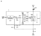
図1は、実施の形態1に係る負荷駆動回路の一例であるLED駆動回路1の回路図である。図1に示されるように、発光ダイオードLED1は、電源VCCと接地点GNDとの間に接続され、通過する電流に応じて発光する電流負荷である。LED駆動回路1は、接地点GNDと発光ダイオードLED1との間に接続されている。LED駆動回路1は、PWM(Pulse Width Modulation)信号を受けて、発光ダイオードLED1に流れる電流を制御する。LED駆動回路1は、DC(Direct Current)変換回路DC1と、差動増幅回路であるオペアンプOP1と、電圧電流変換回路VC1と、カレントミラー回路CM2とを備える。
FIG. 1 is a circuit diagram of an
DC変換回路DC1は、PWM信号を受けてDC電圧に変換し、電圧VinをオペアンプOP1に出力する。オペアンプOP1は、電圧Vinを増幅して電圧Voutを電圧電流変換回路VC1に出力する。電圧電流変換回路VC1は、電圧Voutに応じた電流Iout1をカレントミラー回路CM2に出力する。カレントミラー回路CM2は、電流Iout1を増幅し、発光ダイオードLED1に流れる電流を電流Iout2とする。 The DC conversion circuit DC1 receives the PWM signal, converts it into a DC voltage, and outputs the voltage Vin to the operational amplifier OP1. The operational amplifier OP1 amplifies the voltage Vin and outputs the voltage Vout to the voltage-current conversion circuit VC1. The voltage-current conversion circuit VC1 outputs a current Iout1 corresponding to the voltage Vout to the current mirror circuit CM2. The current mirror circuit CM2 amplifies the current Iout1, and sets the current flowing through the light emitting diode LED1 as the current Iout2.
電流Iout2を安定させるために、LED駆動回路1に抵抗R7、R10、およびR11が接続されている。抵抗R7は、カレントミラー回路CM2と接地点との間に接続されている。抵抗R10は、オペアンプOP1の反転入力端子と抵抗R7との間に接続されている。抵抗R11は、オペアンプOP1の出力端子と抵抗R10との間に接続されている。抵抗R7と抵抗R10との接続点N1の電圧をV11とすると、電圧Voutは、以下の式(1)で表される。
In order to stabilize the current Iout2, resistors R7, R10, and R11 are connected to the
Vout=(1+R11/R10)Vin−(R11/R10)R7・Iout2
…(1)
式(1)より、電流Iout2が大きくなると電圧Voutが小さくなり、その結果、電流Iout2が小さくなるように制御される。逆に電流Iout2が小さくなると電圧Voutが大きくなり、その結果、電流Iout2は大きくなるように制御される。すなわち、電流Iout2には負のフィードバック制御が行なわれる。なお、Iout2が0である場合、電圧Voutは以下の式(2)となる。
Vout = (1 + R11 / R10) Vin− (R11 / R10) R7 · Iout2
... (1)
From the equation (1), when the current Iout2 increases, the voltage Vout decreases, and as a result, the current Iout2 is controlled to decrease. Conversely, when the current Iout2 decreases, the voltage Vout increases, and as a result, the current Iout2 is controlled to increase. That is, negative feedback control is performed on the current Iout2. When Iout2 is 0, the voltage Vout is expressed by the following equation (2).
Vout=(1+R11/R10)Vin …(2)
式(2)の電圧Vinの係数(1+R11/R10)は、オペアンプOP1の増幅率を表す。
Vout = (1 + R11 / R10) Vin (2)
The coefficient (1 + R11 / R10) of the voltage Vin in Expression (2) represents the amplification factor of the operational amplifier OP1.
図2は、比較例に係るLED駆動回路10の回路図である。図2に示されるように、LED駆動回路10は、カレントミラー回路CM11と、カレントミラー回路CM12とを備える。カレントミラー回路CM11には、定電流源CS10によって所定の入力電流が供給される。カレントミラー回路CM12は、カレントミラー回路CM11の出力電流を入力電流とし、当該入力電流を増幅した電流によってLED10を駆動する。このような構成により、LED駆動回路10は、定電流源CS10によって供給された入力電流を、カレントミラー回路CM11およびCM12を用いて増幅してLED10に流すことができる。
FIG. 2 is a circuit diagram of the
LED駆動回路10において、カレントミラー回路に供給される電流は、定電流源に含まれるトランジスタの制御端子に、バイアス調整回路を用いて電圧を印加することによって調整される場合がある。バイアス調整回路によって印加される電圧を上昇させると、当該電圧が当該トランジスタの動作電圧に到達したときにカレントミラー回路に急激に電流が流れ始める。そのため、当該トランジスタの動作電圧を正確に特定することが困難な場合、カレントミラー回路に供給される電流を電圧に応じて線形に制御することが困難になり得る。その結果、LED駆動回路によるLEDの制御が困難になり得る。
In the
そこで、実施の形態1においては、オペアンプOP2の反転入力端子に当該トランジスタの動作電圧(閾値電圧)を印加する。このような構成とすることにより、電圧Voutと閾値電圧とが等しい時に電流Iout1が0となり、電圧Voutと閾値電圧との差に応じて電流Iout1が変化する。すなわち、電圧Voutに対する電流Iout1の線形性が改善される。その結果、電圧Voutに対する電流Iout2の線形性も改善され、発光ダイオードLED1の制御を容易にすることができる。 Therefore, in the first embodiment, the operating voltage (threshold voltage) of the transistor is applied to the inverting input terminal of the operational amplifier OP2. With such a configuration, when the voltage Vout and the threshold voltage are equal, the current Iout1 becomes 0, and the current Iout1 changes according to the difference between the voltage Vout and the threshold voltage. That is, the linearity of the current Iout1 with respect to the voltage Vout is improved. As a result, the linearity of the current Iout2 with respect to the voltage Vout is also improved, and the control of the light emitting diode LED1 can be facilitated.
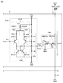
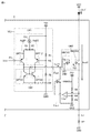
図3は、実施の形態1における電圧電流変換回路VC1の回路構成およびカレントミラー回路CM2の回路構成を併せて示す図である。図3に示されるように、電圧電流変換回路VC1は、電源PS1と接地点GNDとの間に接続される。電圧電流変換回路VC1は、入力端子Pinに印加された電圧Voutに応じた電流Iout1を出力端子Poutから出力するように構成される。電圧電流変換回路VC1は、オペアンプOP2と、カレントミラー回路CM1と、電圧設定部VS1と、抵抗R3,R5とを備える。 FIG. 3 is a diagram illustrating the circuit configuration of the voltage-current conversion circuit VC1 and the circuit configuration of the current mirror circuit CM2 in the first embodiment. As shown in FIG. 3, the voltage / current conversion circuit VC1 is connected between the power supply PS1 and the ground point GND. The voltage-current conversion circuit VC1 is configured to output from the output terminal Pout a current Iout1 corresponding to the voltage Vout applied to the input terminal Pin. The voltage-current conversion circuit VC1 includes an operational amplifier OP2, a current mirror circuit CM1, a voltage setting unit VS1, and resistors R3 and R5.
オペアンプOP2は、電源PS1に接続された定電流源CS1と、PNP型のトランジスタBPT11,トランジスタBPT12と、抵抗R3を含む調節部Adj21と、抵抗R3と抵抗値が等しい抵抗R5を含む調節部Adj22とを含む。 Operational amplifier OP2 includes a constant current source CS1 connected to the power supply PS1, PNP type transistor BPT11, a transistor BPT12, an adjusting unit Adj21 including resistors R3, an adjusting unit Adj22 resistance and the resistor R3 contains an equal resistor R5 including.
カレントミラー回路CM1は、トランジスタBPT11に接続されたNPN型のトランジスタBPT21と、トランジスタBPT12に接続されたNPN型のトランジスタBPT22とを含む。 Current mirror circuit CM1 includes an NPN transistor BPT21 connected to transistor BPT11 and an NPN transistor BPT22 connected to transistor BPT12.
電圧設定部VS1は、抵抗R1とR2とを含む。抵抗R1とR2とは、電源PS1と接地点GNDとの間に直列に接続される。 Voltage setting unit VS1 includes resistors R1 and R2. The resistors R1 and R2 are connected in series between the power source PS1 and the ground point GND.
トランジスタBPT11および12ならびにトランジスタBPT21およびトランジスタBPT22の各々は、制御端子であるベース、エミッタ、およびコレクタを有する。トランジスタBPT11のベースは、入力端子Pinに接続される。トランジスタBPT11のエミッタは、調節部Adj21を介して定電流源CS1に接続される。トランジスタBPT11のコレクタは、トランジスタBPT21のコレクタに接続される。 Transistors BPT11 and B12 and transistors BPT21 and BPT22 each have a base, an emitter, and a collector that are control terminals. The base of the transistor BPT11 is connected to the input terminal Pin. The emitter of the transistor BPT11 is connected to the constant current source CS1 via the adjustment unit Adj21. The collector of the transistor BPT11 is connected to the collector of the transistor BPT21.
トランジスタBPT21のベースは、トランジスタBPT22のベースおよびトランジスタBPT21のコレクタに接続される。トランジスタBPT21のエミッタは、接地点GNDに接続される。 The base of the transistor BPT21 is connected to the base of the transistor BPT22 and the collector of the transistor BPT21. The emitter of the transistor BPT21 is connected to the ground point GND.
トランジスタBPT12のベースは、抵抗R1とR2との接続点N2に接続される。トランジスタBPT12のベースの電圧は、抵抗R1およびR2によりトランジスタBPT12の動作電圧に等しくなるように設定される。トランジスタBPT12のエミッタは、調節部Adj22を介して定電流源CS1に接続される。トランジスタBPT12のコレクタは、トランジスタBPT22のコレクタに接続される。 The base of the transistor BPT12 is connected to a connection point N2 between the resistors R1 and R2. The base voltage of the transistor BPT12 is set to be equal to the operating voltage of the transistor BPT12 by the resistors R1 and R2. The emitter of the transistor BPT12 is connected to the constant current source CS1 via the adjustment unit Adj22. The collector of the transistor BPT12 is connected to the collector of the transistor BPT22.
トランジスタBPT22のエミッタは、接地点GNDに接続される。
出力端子Poutは、トランジスタBPT12のコレクタとトランジスタBPT22のコレクタとの接続点N3に接続される。
The emitter of the transistor BPT22 is connected to the ground point GND.
The output terminal Pout is connected to a connection point N3 between the collector of the transistor BPT12 and the collector of the transistor BPT22.
電圧電流変換回路VC1において、トランジスタBPT11のベースとトランジスタBPT12のベースは、オペアンプOP2の2つの入力端子となる。オペアンプOP2においては、当該2つの入力端子の電圧差が増幅されて、トランジスタBPT11のコレクタの電圧として出力される。トランジスタBPT12のベースの電圧は、抵抗R1およびR2によりトランジスタBPT12の動作電圧(閾値電圧)に等しくなるように設定されているため、トランジスタBPT11に印加される電圧Voutを閾値電圧以上とすることで、電圧Voutと閾値電圧との差に応じてトランジスタBPT11のコレクタの電圧が上昇する。トランジスタBPT11のコレクタは、トランジスタBPT21のコレクタに接続されている。トランジスタBPT21のコレクタは、トランジスタBPT21のベースおよびトランジスタBPT22のベースに接続されている。そのため、トランジスタBPT11のコレクタの電圧が上昇すると、トランジスタBPT21のベースおよびトランジスタBPT22のベースの電圧が上昇して動作電圧に達すると、トランジスタBPT21およびトランジスタBPT22に電流が流れる。トランジスタBPT22に電流が流れると、トランジスタBPT12のコレクタとトランジスタBPT22のコレクタとの接続点N3に接続されている出力端子Poutから電流Iout1が出力される。 In the voltage-current converter circuit VC1, the base of the transistor BPT11 and the base of the transistor BPT12 are two input terminals of the operational amplifier OP2. In the operational amplifier OP2, the voltage difference between the two input terminals is amplified and output as the collector voltage of the transistor BPT11. Since the base voltage of the transistor BPT12 is set to be equal to the operating voltage (threshold voltage) of the transistor BPT12 by the resistors R1 and R2, by setting the voltage Vout applied to the transistor BPT11 to be equal to or higher than the threshold voltage, The collector voltage of the transistor BPT11 increases according to the difference between the voltage Vout and the threshold voltage. The collector of the transistor BPT11 is connected to the collector of the transistor BPT21. The collector of the transistor BPT21 is connected to the base of the transistor BPT21 and the base of the transistor BPT22. Therefore, when the collector voltage of the transistor BPT11 rises, the base voltage of the transistor BPT21 and the base voltage of the transistor BPT22 rise to reach the operating voltage, and a current flows through the transistor BPT21 and the transistor BPT22. When a current flows through the transistor BPT22, a current Iout1 is output from the output terminal Pout connected to the connection point N3 between the collector of the transistor BPT12 and the collector of the transistor BPT22.
電圧電流変換回路VC1によれば、オペアンプOP2の2つの入力端子の電圧差に応じた電流Iout1が出力される。すなわち、電圧Voutが閾値電圧に等しい場合、電流Iout1は出力されず、電圧Voutの上昇に伴って電流Iout1が上昇する。その結果、電圧Voutに対する電流Iout2の線形性が改善され、発光ダイオードLED1の制御を容易に行なうことができる。 According to the voltage-current converter circuit VC1, a current Iout1 corresponding to the voltage difference between the two input terminals of the operational amplifier OP2 is output. That is, when the voltage Vout is equal to the threshold voltage, the current Iout1 is not output, and the current Iout1 increases as the voltage Vout increases. As a result, the linearity of the current Iout2 with respect to the voltage Vout is improved, and the light emitting diode LED1 can be easily controlled.
また、調節部Adj21,Adj22は、電圧Voutと電流Iout2との間の変換係数を調節する。 Further, the adjustment units Adj21 and Adj22 adjust a conversion coefficient between the voltage Vout and the current Iout2.
電圧Voutと電流Iout1との比(変換係数)をk1とすると、電流Iout1は式(3)のように表すことができる。 When the ratio (conversion coefficient) between the voltage Vout and the current Iout1 is k1, the current Iout1 can be expressed as in Expression (3).
Iout1=k1・Vout …(3)
電流Iout1とIout2との比であるカレントミラー比をk2とすると、電流Iout2は式(4)のように表すことができる。
Iout1 = k1 · Vout (3)
When the current mirror ratio, which is the ratio between the currents Iout1 and Iout2, is k2, the current Iout2 can be expressed as in Expression (4).
Iout2=k2・Iout1 …(4)
式(4)の電流Iout1に式(3)を代入することにより、電流Iout2は電圧Voutを用いて式(5)のように表すことができる。式(5)において、k3=k2・k1である。変換係数k3は、電圧Voutと電流Iout2との比(変換係数)である。
Iout2 = k2 · Iout1 (4)
By substituting the equation (3) into the current Iout1 of the equation (4), the current Iout2 can be expressed as the equation (5) using the voltage Vout. In Equation (5), k3 = k2 · k1. The conversion coefficient k3 is a ratio (conversion coefficient) between the voltage Vout and the current Iout2.
Iout2=k2・k1・Vout=k3・Vout …(5)
式(5)から変換係数k3は、式(6)のように表すことができる。抵抗R3およびR5の抵抗値が大きくなると、オペアンプOP2を流れる電流は小さくなる。電流Iout1が小さくなって、電流Iout2が小さくなる。その結果、式(6)より、変換係数k3は小さくなる。逆に抵抗R3およびR5の抵抗値が小さくなると、オペアンプOP2を流れる電流は大きくなる。電流Iout1が大きくなって、電流Iout2が大きくなる。その結果、式(6)より変換係数k3は大きくなる。このように、抵抗R3およびR5の値を変化させることにより、変換係数k3を調節することができる。
Iout2 = k2, k1, Vout = k3, Vout (5)
From equation (5), the conversion coefficient k3 can be expressed as in equation (6). As the resistance values of the resistors R3 and R5 increase, the current flowing through the operational amplifier OP2 decreases. The current Iout1 is reduced and the current Iout2 is reduced. As a result, the conversion coefficient k3 becomes smaller from Equation (6). Conversely, when the resistance values of the resistors R3 and R5 are reduced, the current flowing through the operational amplifier OP2 is increased. The current Iout1 increases and the current Iout2 increases. As a result, the conversion coefficient k3 becomes larger from Equation (6). Thus, the conversion coefficient k3 can be adjusted by changing the values of the resistors R3 and R5.
k3=Iout2/Vout …(6)
カレントミラー回路CM2は、電圧電流変換回路VC1から出力された電流Iout1を受けて、電流Iout1を増幅して発光ダイオードLED1に流れる電流を電流Iout2とする。カレントミラー回路CM2は、トランジスタNMOS3と、トランジスタNMOS4とを含む。トランジスタNMOS3およびトランジスタNMOS4の各々は、ゲート、ソース、およびドレインを有する。トランジスタNMOS3のゲートは、トランジスタNMOS4のゲートおよびトランジスタNMOS3のドレインに接続される。トランジスタNMOS3のソースは、接地点GNDに接続される。トランジスタNMOS3のドレインは、電圧電流変換回路VC1の出力端子Poutに接続される。トランジスタNMOS4のソースは、抵抗R7を介して接地点GNDに接続される。トランジスタNMOS4のドレインは、発光ダイオードLED1を介して電源VCCに接続される。
k3 = Iout2 / Vout (6)
The current mirror circuit CM2 receives the current Iout1 output from the voltage-current conversion circuit VC1, amplifies the current Iout1, and sets the current flowing through the light emitting diode LED1 as the current Iout2. The current mirror circuit CM2 includes a transistor NMOS3 and a transistor NMOS4. Each of the transistors NMOS3 and NMOS4 has a gate, a source, and a drain. The gate of the transistor NMOS3 is connected to the gate of the transistor NMOS4 and the drain of the transistor NMOS3. The source of the transistor NMOS3 is connected to the ground point GND. The drain of the transistor NMOS3 is connected to the output terminal Pout of the voltage / current converter circuit VC1. The source of the transistor NMOS4 is connected to the ground point GND through the resistor R7. The drain of the transistor NMOS4 is connected to the power supply VCC via the light emitting diode LED1.
実施の形態1において、電圧電流変換回路VC1から電流Iout1が入力されるトランジスタNMOS3のソースの電圧は、トランジスタNMOS4のソースの電圧よりも抵抗R7の分だけ低い。このような構成とすることにより、トランジスタNMOS3のソースがトランジスタNMOS4のソースに接続されて両者が同電位である場合よりも、トランジスタNMOS3が動作することのできる電圧の範囲が広くなる。その結果、カレントミラー回路CM2が動作することのできる電圧の範囲を広くすることができる。 In the first embodiment, the source voltage of the transistor NMOS3 to which the current Iout1 is input from the voltage-current conversion circuit VC1 is lower than the source voltage of the transistor NMOS4 by the resistance R7. With such a configuration, the voltage range in which the transistor NMOS3 can operate becomes wider than when the source of the transistor NMOS3 is connected to the source of the transistor NMOS4 and both have the same potential. As a result, the voltage range in which the current mirror circuit CM2 can operate can be widened.
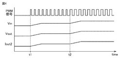
図4は、PWM信号、DC変換回路DC1の出力である電圧Vin、オペアンプOP1の出力である電圧Vout、および発光ダイオードLED1に流れる電流Iout2のタイムチャートを併せて示す図である。図4に示されるように、時刻t1から或るデューティ比のPWM信号が入力され、電圧Vinが上昇している。電圧Vinの上昇に応じて、電圧Voutが上昇し、その結果、電流Iout2が上昇している。電圧Vinの上昇が止まると、電圧Voutおよび電流Iout2の上昇も止まっている。時刻t2からPWM信号のデューティ比が大きくなり、電圧Vinがさらに上昇している。電圧Vinの上昇に伴い、電圧Voutが上昇し、その結果、電流Iout2が上昇している。このように、PWM信号によって電圧VinおよびVoutを制御することにより、発光ダイオードLED1に流れる電流Iout2を制御することができる。その結果、発光ダイオードLED1の制御を容易に行なうことができる。 FIG. 4 is a diagram illustrating a time chart of the PWM signal, the voltage Vin that is the output of the DC conversion circuit DC1, the voltage Vout that is the output of the operational amplifier OP1, and the current Iout2 that flows through the light emitting diode LED1. As shown in FIG. 4, a PWM signal having a certain duty ratio is input from time t1, and the voltage Vin increases. As the voltage Vin increases, the voltage Vout increases, and as a result, the current Iout2 increases. When the increase of the voltage Vin stops, the increase of the voltage Vout and the current Iout2 also stops. From time t2, the duty ratio of the PWM signal increases and the voltage Vin further increases. As the voltage Vin increases, the voltage Vout increases, and as a result, the current Iout2 increases. Thus, by controlling the voltages Vin and Vout with the PWM signal, the current Iout2 flowing through the light emitting diode LED1 can be controlled. As a result, it is possible to easily control the light emitting diode LED1.
以上、実施の形態1に係る負荷駆動回路によれば、電圧電流変換回路の差動増幅回路の一方の入力端子にトランジスタの動作電圧を設定することにより、当該差動増幅回路の2つの入力端子の電圧差に応じた電流が出力端子から出力される。その結果、入力電圧に対する出力電流の線形性が改善され、電流負荷の制御を容易にすることができる。 As described above, according to the load driving circuit according to the first embodiment, by setting the operating voltage of the transistor to one input terminal of the differential amplifier circuit of the voltage-current conversion circuit, the two inputs of the differential amplifier circuit A current corresponding to the voltage difference between the terminals is output from the output terminal. As a result, the linearity of the output current with respect to the input voltage is improved, and the current load can be easily controlled.
さらに、実施の形態1に係る負荷駆動回路によれば、調節部に含まれる抵抗値を変化させることにより、入力電圧と出力電流との間の変換率を電流負荷に適した値に調節することができる。その結果、電流負荷の制御の精度を向上させることができる。 Furthermore, according to the load drive circuit according to the first embodiment, the conversion ratio between the input voltage and the output current is adjusted to a value suitable for the current load by changing the resistance value included in the adjustment unit. Can do. As a result, the accuracy of current load control can be improved.
実施の形態2.
実施の形態1においては、各調節部が、1つの抵抗を含んでいる場合について説明した。抵抗は温度によって抵抗値が変化する場合がある。抵抗値が変化すると電圧Voutと電流Iout2との間の変換係数が変化してしまい、発光ダイオードLED1の制御の精度が低下し得る。そこで、実施の形態2では、変換係数のこのような温度依存性を抑制する構成について説明する。
In the first embodiment, a case has been described in which each adjustment unit includes one resistor. The resistance value of the resistor may change depending on the temperature. When the resistance value changes, the conversion coefficient between the voltage Vout and the current Iout2 changes, and the accuracy of control of the light emitting diode LED1 can be reduced. In the second embodiment, a configuration for suppressing such temperature dependence of the conversion coefficient will be described.
実施の形態2と1との違いは、各調節部が正の温度特性を有する抵抗と、負の温度特性を有する抵抗とを含む点である。それ以外の構成については同様であるため、その説明は繰り返さない。
The difference between
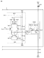
図5は、実施の形態2における電圧電流変換回路VC2の回路構成およびカレントミラー回路CM2の回路構成を併せて示す図である。図5に示されるように、オペアンプOP22は、図1の調節部Adj21およびAdj22に代わって調節部Adj221およびAdj222をそれぞれ含む。調節部Adj221は、直列に接続された抵抗R23とR24を含む。調節部Adj222は、直列に接続された抵抗R25とR26とを含む。抵抗R23の抵抗値は、抵抗R25の抵抗値に等しい。抵抗R23およびR25は、正の温度特性を有する。抵抗R24の抵抗値は、抵抗R26の抵抗値に等しい。抵抗R24および抵抗R26は、負の温度特性を有する。 FIG. 5 is a diagram illustrating the circuit configuration of the voltage-current conversion circuit VC2 and the circuit configuration of the current mirror circuit CM2 in the second embodiment. As shown in FIG. 5, the operational amplifier OP22 includes adjustment units Adj221 and Adj222 in place of the adjustment units Adj21 and Adj22 of FIG. Adjustment unit Adj221 includes resistors R23 and R24 connected in series. Adjustment unit Adj222 includes resistors R25 and R26 connected in series. The resistance value of the resistor R23 is equal to the resistance value of the resistor R25. Resistors R23 and R25 have positive temperature characteristics. The resistance value of the resistor R24 is equal to the resistance value of the resistor R26. The resistor R24 and the resistor R26 have negative temperature characteristics.
電圧電流変換回路VC2の温度が上昇した場合、正の温度特性を有する抵抗R23およびR25の抵抗値は上昇する。一方、負の温度特性を持つ抵抗R24およびR26の抵抗値は低下する。逆に、電圧電流変換回路VC2の温度が低下した場合、正の温度特性を有する抵抗R23およびR25の抵抗値は低下する。一方、負の温度特性を持つ抵抗R24およびR26の抵抗値は上昇する。そのため、電圧電流変換回路VC2の温度が変化しても、抵抗R23およびR24を含む調節部Adj221の抵抗値および抵抗R25およびR26を含む調節部Adj222の抵抗値はほとんど変わらない。その結果、変換係数の温度依存性を抑制することができる。 When the temperature of the voltage-current conversion circuit VC2 rises, the resistance values of the resistors R23 and R25 having positive temperature characteristics rise. On the other hand, the resistance values of the resistors R24 and R26 having negative temperature characteristics are lowered. Conversely, when the temperature of the voltage-current converter circuit VC2 is lowered, the resistance values of the resistors R23 and R25 having positive temperature characteristics are lowered. On the other hand, the resistance values of the resistors R24 and R26 having negative temperature characteristics increase. Therefore, even if the temperature of the voltage-current conversion circuit VC2 changes, the resistance value of the adjustment unit Adj221 including the resistors R23 and R24 and the resistance value of the adjustment unit Adj222 including the resistors R25 and R26 are hardly changed. As a result, the temperature dependence of the conversion coefficient can be suppressed.
以上、実施の形態2に係る負荷駆動回路によれば、実施の形態1と同様に電流負荷の制御を容易にすることができるとともに、電流負荷の制御の精度を向上させることができる。 As described above, according to the load drive circuit according to the second embodiment, it is possible to easily control the current load as in the first embodiment, and to improve the accuracy of the control of the current load.
さらに実施の形態2に係る負荷駆動回路によれば、調節部が正の温度特性をもつ抵抗と負の温度特性をもつ抵抗とを含むことにより、入力電圧と出力電流との間の変換係数の温度依存性を抑制することができる。その結果、電流負荷を安定的に制御することができる。 Furthermore, according to the load driving circuit according to the second embodiment, the adjustment unit includes a resistor having a positive temperature characteristic and a resistor having a negative temperature characteristic, so that the conversion coefficient between the input voltage and the output current can be reduced. Temperature dependence can be suppressed. As a result, the current load can be stably controlled.
実施の形態3.
実施の形態1においては、電圧電流変換回路VC1から電流Iout1が入力されるトランジスタNMOS3のソースの電圧が、トランジスタNMOS4のソースの電圧よりも抵抗R7の分だけ低い場合について説明した。このような構成により、上述したようにカレントミラー回路CM2が動作することのできる電圧の範囲を広くすることができる。しかし、トランジスタNMOS3のソースの電圧と、トランジスタNMOS4のソースの電圧とが異なると、トランジスタNMOS3のゲート−ソース間の電圧と、トランジスタNMOS4のゲート−ソース間の電圧との間に差異が生じる。また、トランジスタNMOS3のドレイン−ソース間の電圧と、トランジスタNMOS4のドレイン−ソース間の電圧との間にも差異が生じる。その結果、カレントミラー回路CM2のカレントミラー比の精度が低下してしまう可能性がある。したがって、カレントミラー回路CM2を動作させる電圧の範囲が限定されている場合には、トランジスタNMOS3のソースとトランジスタNMOS4のソースとは同電位であることが望ましい。
In the first embodiment, the case where the source voltage of the transistor NMOS3 to which the current Iout1 is input from the voltage-current conversion circuit VC1 is lower than the source voltage of the transistor NMOS4 by the resistance R7 has been described. With this configuration, as described above, the voltage range in which the current mirror circuit CM2 can operate can be widened. However, if the source voltage of the transistor NMOS3 and the source voltage of the transistor NMOS4 are different, a difference is generated between the gate-source voltage of the transistor NMOS3 and the gate-source voltage of the transistor NMOS4. In addition, a difference also occurs between the drain-source voltage of the transistor NMOS3 and the drain-source voltage of the transistor NMOS4. As a result, the accuracy of the current mirror ratio of the current mirror circuit CM2 may be reduced. Therefore, when the voltage range for operating the current mirror circuit CM2 is limited, it is desirable that the source of the transistor NMOS3 and the source of the transistor NMOS4 have the same potential.
そこで、実施の形態3においては、カレントミラー回路CM2に含まれるトランジスタNMOS3およびNMOS4のそれぞれのソースが同電位である場合について説明する。このような構成とすることにより、カレントミラー回路CM2のカレントミラー比を向上させることができる。 Therefore, in the third embodiment, a case will be described in which the sources of the transistors NMOS3 and NMOS4 included in the current mirror circuit CM2 are at the same potential. With such a configuration, the current mirror ratio of the current mirror circuit CM2 can be improved.
実施の形態3と1との違いは、カレントミラー回路CM2に含まれるトランジスタNMOS3とNMOS4のそれぞれのソースが同電位であるという点である。それ以外の点については同様であるため、その説明は繰り返さない。 The difference between the third and first embodiments is that the sources of the transistors NMOS3 and NMOS4 included in the current mirror circuit CM2 have the same potential. Since it is the same about other points, the description will not be repeated.
図6は、実施の形態3における電圧電流変換回路VC1の回路構成およびカレントミラー回路CM32の回路構成を併せて示す図である。図6に示されるように、カレントミラー回路CM32に含まれるトランジスタNMOS3のソースは、トランジスタNMOS4のソースに接続されている。このようにトランジスタNMOS3のソースと、トランジスタNMOS3のソースとを同電位とすることにより、トランジスタNMOS3のゲート−ソース間の電圧と、トランジスタNMOS4のゲート−ソース間の電圧とが同じになる。また、トランジスタNMOS3のドレイン−ソース間の電圧と、トランジスタNMOS4のドレイン−ソース間の電圧とが同じになる。その結果、カレントミラー回路CM2のカレントミラー比を向上させることができる。 FIG. 6 is a diagram illustrating the circuit configuration of the voltage-current conversion circuit VC1 and the circuit configuration of the current mirror circuit CM32 in the third embodiment. As shown in FIG. 6, the source of the transistor NMOS3 included in the current mirror circuit CM32 is connected to the source of the transistor NMOS4. Thus, by setting the source of the transistor NMOS3 and the source of the transistor NMOS3 to the same potential, the voltage between the gate and the source of the transistor NMOS3 and the voltage between the gate and the source of the transistor NMOS4 become the same. Further, the voltage between the drain and the source of the transistor NMOS3 is the same as the voltage between the drain and the source of the transistor NMOS4. As a result, the current mirror ratio of the current mirror circuit CM2 can be improved.
以上、実施の形態3に係る負荷駆動回路によれば、実施の形態1と同様に電流負荷の制御を容易にすることができるとともに、電流負荷の制御の精度を向上させることができる。 As described above, according to the load driving circuit according to the third embodiment, it is possible to easily control the current load as in the first embodiment, and to improve the accuracy of the control of the current load.
さらに実施の形態3に係る負荷駆動回路によれば、電圧電流変換回路からの電流を受けるカレントミラー回路のカレントミラー比を向上させることができる。 Furthermore, according to the load drive circuit according to the third embodiment, the current mirror ratio of the current mirror circuit that receives the current from the voltage-current conversion circuit can be improved.
実施の形態4.
図1に示されたLED駆動回路1において、発光ダイオードLED1に過電流が流れる異常、あるいは電源電圧が低下する異常などが発生する場合がある。このような場合に発光ダイオードLED1の駆動を継続していると、発光ダイオードLED1あるいはLED駆動回路1が故障して停止してしまうおそれがある。そこで、実施の形態4においては、このような異常を検出する異常検出回路を備える負荷駆動回路について説明する。
In the
実施の形態4と1との違いは、異常検出回路の有無である。それ以外の点については同様であるため、その説明は繰り返さない。
The difference between
図7は、実施の形態4に係る負荷駆動回路の一例であるLED駆動回路4の回路図である。図7に示されるように、LED駆動回路4は、図1に示されるLED駆動回路1の構成に加えて、異常検出回路Edc1をさらに備える。異常検出回路Edc1は、発光ダイオードLED1に過電流が流れた場合に、カレントミラー回路CM2の動作を停止させる。
FIG. 7 is a circuit diagram of an
図8は、実施の形態4における電圧電流変換回路VC1の回路構成、カレントミラー回路CM2の回路構成、および異常検出回路Edc1の回路構成を併せて示す図である。 FIG. 8 is a diagram illustrating the circuit configuration of the voltage-current conversion circuit VC1, the circuit configuration of the current mirror circuit CM2, and the circuit configuration of the abnormality detection circuit Edc1 according to the fourth embodiment.
異常検出回路Edc1は、コンパレータCmp1と、トランジスタNMOS5と、抵抗R8,R9とを含む。トランジスタNMOS5のゲートは、コンパレータCmp1の出力端子に接続される。トランジスタNMOS5のソースは、接地点GNDに接続される。トランジスタNMOS5のドレインは、トランジスタNMOS3のドレインに接続される。抵抗R8とR9とは、電源PS1と接地点GNDとの間に直列に接続される。コンパレータCmp1の非反転入力端子は、トランジスタNMOS4のソースに接続される。コンパレータCmp1の反転入力端子は、抵抗R8とR9との接続点N4に接続される。 The abnormality detection circuit Edc1 includes a comparator Cmp1, a transistor NMOS5, and resistors R8 and R9. The gate of the transistor NMOS5 is connected to the output terminal of the comparator Cmp1. The source of the transistor NMOS5 is connected to the ground point GND. The drain of the transistor NMOS5 is connected to the drain of the transistor NMOS3. Resistors R8 and R9 are connected in series between power supply PS1 and ground point GND. The non-inverting input terminal of the comparator Cmp1 is connected to the source of the transistor NMOS4. The inverting input terminal of the comparator Cmp1 is connected to the connection point N4 between the resistors R8 and R9.
発光ダイオードLED1に過電流が流れた場合、過電流が抵抗R7を通過するときの電圧降下が大きくなり、抵抗R7に接続しているトランジスタNMOS4のソースの電圧が上昇する。コンパレータCmp1の非反転入力端子は、トランジスタNMOS4のソースに接続されているから、過電流が流れるとコンパレータCmp1からHighレベルの電圧が出力される。コンパレータCmp1の出力端子は、トランジスタNMOS5のゲートに接続されているから、コンパレータCmp1の出力電圧がトランジスタNMOS5の動作電圧に達したときにトランジスタNMOS5が導通する。トランジスタNMOS5のドレインは、トランジスタNMOS3のドレインに接続されているから、トランジスタNMOS5が導通することにより、トランジスタNMOS3のドレインと接地点GNDとが導通する。その結果、トランジスタNMOS3のドレインの電圧が降下する。トランジスタNMOS3のドレインはトランジスタNMOS3のゲートに接続されているから、トランジスタNMOS3のドレインの電圧が降下すると、トランジスタNMOS3のゲートの電圧が降下する。トランジスタNMOS3のゲートはトランジスタNMOS4のゲートに接続されているから、トランジスタNMOS3のゲートの電圧が動作電圧より小さくなると、トランジスタNMOS3およびNMOS4に電流が流れなくなる。その結果、カレントミラー回路CM2は動作を停止する。 When an overcurrent flows through the light emitting diode LED1, a voltage drop when the overcurrent passes through the resistor R7 increases, and a voltage of the source of the transistor NMOS4 connected to the resistor R7 increases. Since the non-inverting input terminal of the comparator Cmp1 is connected to the source of the transistor NMOS4, a high level voltage is output from the comparator Cmp1 when an overcurrent flows. Since the output terminal of the comparator Cmp1 is connected to the gate of the transistor NMOS5, the transistor NMOS5 becomes conductive when the output voltage of the comparator Cmp1 reaches the operating voltage of the transistor NMOS5. Since the drain of the transistor NMOS5 is connected to the drain of the transistor NMOS3, when the transistor NMOS5 is turned on, the drain of the transistor NMOS3 and the ground point GND are turned on. As a result, the voltage at the drain of the transistor NMOS3 drops. Since the drain of the transistor NMOS3 is connected to the gate of the transistor NMOS3, when the voltage at the drain of the transistor NMOS3 drops, the voltage at the gate of the transistor NMOS3 drops. Since the gate of the transistor NMOS3 is connected to the gate of the transistor NMOS4, when the gate voltage of the transistor NMOS3 becomes lower than the operating voltage, no current flows through the transistors NMOS3 and NMOS4. As a result, the current mirror circuit CM2 stops operating.
異常検出回路によって電源電圧を検知して、電源電圧が所定の電圧以下となった場合に、カレントミラー回路CM2を停止させてもよい。 The current mirror circuit CM2 may be stopped when the power supply voltage is detected by the abnormality detection circuit and the power supply voltage falls below a predetermined voltage.
以上、実施の形態4に係る負荷駆動回路によれば、実施の形態1と同様に電流負荷の制御を容易にすることができるとともに、電流負荷の制御の精度を向上させることができる。 As described above, according to the load driving circuit according to the fourth embodiment, it is possible to easily control the current load as in the first embodiment, and it is possible to improve the accuracy of the control of the current load.
さらに実施の形態4に係る負荷駆動回路によれば、異常の発生を異常検出回路によって検出することにより、異常の発生の直後に負荷駆動回路を停止させることができる。その結果、負荷駆動回路あるいは電流負荷の故障を防止することができる。 Furthermore, according to the load drive circuit of the fourth embodiment, the load drive circuit can be stopped immediately after the occurrence of the abnormality by detecting the occurrence of the abnormality with the abnormality detection circuit. As a result, failure of the load drive circuit or current load can be prevented.
今回開示された各実施の形態は、矛盾しない範囲で適宜組合わせて実施することも予定されている。今回開示された実施の形態はすべての点で例示であって制限的なものではないと考えられるべきである。本発明の範囲は上記した説明ではなくて特許請求の範囲によって示され、特許請求の範囲と均等の意味および範囲内でのすべての変更が含まれることが意図される。 The embodiments disclosed herein are also scheduled to be implemented in appropriate combinations within a consistent range. The embodiment disclosed this time should be considered as illustrative in all points and not restrictive. The scope of the present invention is defined by the terms of the claims, rather than the description above, and is intended to include any modifications within the scope and meaning equivalent to the terms of the claims.
1,4,10 LED駆動回路、Adj21,Adj22,Adj221,Adj222 調節部、BPT11,BPT12,BPT21,BPT22,NMO3,NMOS3,NMOS4,NMOS5 トランジスタ、CM1,CM11,CM12,CM32 カレントミラー回路、CS1,CS10 定電流源、Cmp1 コンパレータ、DC1 DC変換回路、Edc1 異常検出回路、GND 接地点、LED1 発光ダイオード、OP1,OP2,OP22 オペアンプ、PS1,VCC 電源、Pout 出力端子、R1,R2,R3,R5,R7,R8,R9,R10,R11,R23,R24,R25,R26 抵抗、VC1,VC2 電圧電流変換回路。 1,4,10 LED drive circuit, Adj21, Adj22, Adj221, Adj222 adjustment unit, BPT11, BPT12, BPT21, BPT22, NMO3, NMOS3, NMOS4, NMOS5 transistor, CM1, CM11, CM12, CM32 current mirror circuit, CS1, CS10 Constant current source, Cmp1 comparator, DC1 DC conversion circuit, Edc1 abnormality detection circuit, GND grounding point, LED1 light emitting diode, OP1, OP2, OP22 operational amplifier, PS1, VCC power supply, Pout output terminal, R1, R2, R3, R5, R7 , R8, R9, R10, R11, R23, R24, R25, R26 resistors, VC1, VC2 voltage-current conversion circuit.
Claims (7)
前記入力端子から前記入力電圧を受けて、前記入力電圧と閾値電圧との差に応じた電圧を出力するように構成された差動増幅回路と、
前記差動増幅回路からの電圧を受け、前記出力端子に前記出力電流を出力するように構成された第1カレントミラー回路と、
前記閾値電圧を設定するように構成された電圧設定部とを備え、
前記差動増幅回路は、前記第1電源に接続された定電流源と、第1トランジスタと、第2トランジスタとを含み、
前記第1カレントミラー回路は、前記第1トランジスタに接続された第3トランジスタと、前記第2トランジスタに接続された第4トランジスタとを含み、
前記電圧設定部は、前記第1電源と前記接地点との間に直列に接続された第1抵抗と第2抵抗とを含み、
前記第1トランジスタおよび前記第2トランジスタの各々は第1導電型トランジスタであり、
前記第3トランジスタおよび前記第4トランジスタの各々は第2導電型トランジスタであり、
前記第1トランジスタおよび前記第2トランジスタならびに前記第3トランジスタおよび前記第4トランジスタの各々は、制御端子、第1端子、および第2端子を有し、
前記第1トランジスタの制御端子は、前記入力端子に接続され、
前記第1トランジスタの第1端子は、前記定電流源に接続され、
前記第1トランジスタの第2端子は、前記第3トランジスタの第2端子に接続され、
前記第3トランジスタの制御端子は、前記第4トランジスタの制御端子および前記第3トランジスタの第2端子に接続され、
前記第3トランジスタの第1端子は、前記接地点に接続され、
前記第2トランジスタの制御端子は、前記第1抵抗と前記第2抵抗との接続点に接続され、
前記第2トランジスタの制御端子の電圧は、前記第1抵抗および前記第2抵抗により前記第2トランジスタの動作電圧となるように設定され、
前記第2トランジスタの第1端子は、前記定電流源に接続され、
前記第2トランジスタの第2端子は、前記第4トランジスタの第2端子に接続され、
前記第4トランジスタの第1端子は、前記接地点に接続され、
前記出力端子は、前記第2トランジスタの第2端子と前記第4トランジスタの第2端子との接続点に接続される、電圧電流変換回路。 A voltage-current conversion circuit connected between a first power source and a ground point and configured to output an output current corresponding to an input voltage applied to an input terminal from the output terminal;
A differential amplifier circuit configured to receive the input voltage from the input terminal and output a voltage corresponding to a difference between the input voltage and a threshold voltage;
A first current mirror circuit configured to receive a voltage from the differential amplifier circuit and to output the output current to the output terminal;
And a voltage setting unit configured to set the threshold voltage,
The differential amplifier circuit includes a constant current source connected to the first power source, a first transistor, and a second transistor,
The first current mirror circuit includes a third transistor connected to the first transistor and a fourth transistor connected to the second transistor,
The voltage setting unit includes a first resistor and a second resistor connected in series between the first power source and the ground point,
Each of the first transistor and the second transistor is a first conductivity type transistor,
Each of the third transistor and the fourth transistor is a second conductivity type transistor,
Each of the first transistor, the second transistor, the third transistor, and the fourth transistor has a control terminal, a first terminal, and a second terminal;
A control terminal of the first transistor is connected to the input terminal;
A first terminal of the first transistor is connected to the constant current source;
A second terminal of the first transistor is connected to a second terminal of the third transistor;
A control terminal of the third transistor is connected to a control terminal of the fourth transistor and a second terminal of the third transistor;
A first terminal of the third transistor is connected to the ground point;
A control terminal of the second transistor is connected to a connection point between the first resistor and the second resistor;
The voltage of the control terminal of the second transistor is set to be the operating voltage of the second transistor by the first resistor and the second resistor,
A first terminal of the second transistor is connected to the constant current source;
A second terminal of the second transistor is connected to a second terminal of the fourth transistor;
A first terminal of the fourth transistor is connected to the ground point;
The output terminal is connected to a connection point between a second terminal of the second transistor and a second terminal of the fourth transistor.
前記第1調節部は、前記定電流源と前記第1トランジスタの第1端子との間に接続され、
前記第2調節部は、前記定電流源と前記第2トランジスタの第1端子との間に接続され、
前記第1調節部の抵抗値は、前記第2調節部の抵抗値に等しい、請求項1に記載の電圧電流変換回路。 The differential amplifier circuit further includes a first adjustment unit and a second adjustment unit for adjusting a conversion coefficient between the input voltage and the output current,
The first adjustment unit is connected between the constant current source and a first terminal of the first transistor,
The second adjustment unit is connected between the constant current source and a first terminal of the second transistor,
Wherein the resistance value of the first adjustment unit is equal to the resistance value of the second adjusting unit, the voltage-current conversion circuit according to claim 1.
前記第2調節部は、直列に接続された第5抵抗と第6抵抗とを含み、
前記第3抵抗の抵抗値は、前記第5抵抗の抵抗値に等しく、
前記第3抵抗および前記第5抵抗は、正の温度特性を有し、
前記第4抵抗の抵抗値は、前記第6抵抗の抵抗値に等しく、
前記第4抵抗および前記第6抵抗は、負の温度特性を有する、請求項2に記載の電圧電流変換回路。 The first adjustment unit includes a third resistor and a fourth resistor connected in series,
The second adjustment unit includes a fifth resistor and a sixth resistor connected in series,
The resistance value of the third resistor is equal to the resistance value of the fifth resistor,
The third resistor and the fifth resistor have positive temperature characteristics,
The resistance value of the fourth resistor is equal to the resistance value of the sixth resistor,
The voltage-current converter circuit according to claim 2 , wherein the fourth resistor and the sixth resistor have negative temperature characteristics.
請求項1に記載の電圧電流変換回路と、
第5トランジスタと、第6トランジスタとを含む第2カレントミラー回路とを備え、
前記負荷は、第2電源と前記接地点との間に接続されており、
前記第5トランジスタおよび前記第6トランジスタの各々は、制御端子、第1端子、および第2端子を有し、
前記第5トランジスタの制御端子は、前記第6トランジスタの制御端子および前記第5トランジスタの第2端子に接続され、
前記第5トランジスタの第1端子の電圧は、前記第6トランジスタの第1端子の電圧以下であり、
前記第5トランジスタの第2端子は、前記電圧電流変換回路の出力端子に接続され、
前記第6トランジスタの第1端子は、第7抵抗を介して前記接地点に接続され、
前記第6トランジスタの第2端子は、前記負荷を介して前記第2電源に接続される、負荷駆動回路。 A load driving circuit for driving a load,
The voltage-current converter circuit according to claim 1;
A second current mirror circuit including a fifth transistor and a sixth transistor;
The load is connected between a second power source and the ground point,
Each of the fifth transistor and the sixth transistor has a control terminal, a first terminal, and a second terminal;
A control terminal of the fifth transistor is connected to a control terminal of the sixth transistor and a second terminal of the fifth transistor;
The voltage of the first terminal of the fifth transistor is equal to or lower than the voltage of the first terminal of the sixth transistor;
A second terminal of the fifth transistor is connected to an output terminal of the voltage-current converter;
A first terminal of the sixth transistor is connected to the ground point via a seventh resistor;
The load driving circuit, wherein a second terminal of the sixth transistor is connected to the second power supply via the load.
反転入力端子、非反転入力端子、および出力端子を有するコンパレータと、
前記コンパレータの出力端子に接続された制御端子と、前記接地点に接続された第1端子と、前記第5トランジスタの第2端子に接続された第2端子とを有する第7トランジスタと、
前記第1電源と前記接地点との間に直列に接続された第8抵抗と第9抵抗とを含み、
前記非反転入力端子は、前記第6トランジスタの第1端子に接続され、
前記反転入力端子は、前記第8抵抗と前記第9抵抗との接続点に接続される、請求項6に記載の負荷駆動回路。 The abnormality detection circuit is
A comparator having an inverting input terminal, a non-inverting input terminal, and an output terminal;
A seventh transistor having a control terminal connected to the output terminal of the comparator; a first terminal connected to the ground; and a second terminal connected to the second terminal of the fifth transistor;
An eighth resistor and a ninth resistor connected in series between the first power source and the ground point;
The non-inverting input terminal is connected to a first terminal of the sixth transistor;
The load drive circuit according to claim 6 , wherein the inverting input terminal is connected to a connection point between the eighth resistor and the ninth resistor.
Priority Applications (3)
| Application Number | Priority Date | Filing Date | Title |
|---|---|---|---|
| JP2016127559A JP6576306B2 (en) | 2016-06-28 | 2016-06-28 | Voltage-current conversion circuit and load drive circuit |
| US15/453,747 US10345833B2 (en) | 2016-06-28 | 2017-03-08 | Voltage-current converter and load driver |
| CN201710508382.2A CN107548202B (en) | 2016-06-28 | 2017-06-28 | Voltage current transformating circuit and load driving circuits |
Applications Claiming Priority (1)
| Application Number | Priority Date | Filing Date | Title |
|---|---|---|---|
| JP2016127559A JP6576306B2 (en) | 2016-06-28 | 2016-06-28 | Voltage-current conversion circuit and load drive circuit |
Publications (3)
| Publication Number | Publication Date |
|---|---|
| JP2018005323A JP2018005323A (en) | 2018-01-11 |
| JP2018005323A5 JP2018005323A5 (en) | 2018-07-12 |
| JP6576306B2 true JP6576306B2 (en) | 2019-09-18 |
Family
ID=60677318
Family Applications (1)
| Application Number | Title | Priority Date | Filing Date |
|---|---|---|---|
| JP2016127559A Active JP6576306B2 (en) | 2016-06-28 | 2016-06-28 | Voltage-current conversion circuit and load drive circuit |
Country Status (3)
| Country | Link |
|---|---|
| US (1) | US10345833B2 (en) |
| JP (1) | JP6576306B2 (en) |
| CN (1) | CN107548202B (en) |
Families Citing this family (9)
| Publication number | Priority date | Publication date | Assignee | Title |
|---|---|---|---|---|
| CN110073614B (en) * | 2016-08-30 | 2022-03-04 | Macom技术解决方案控股公司 | Driver with distributed architecture |
| JP6797849B2 (en) * | 2018-01-26 | 2020-12-09 | 株式会社東芝 | Voltage-current conversion circuit |
| DE112018000110T5 (en) * | 2018-02-08 | 2019-10-02 | Dialog Semiconductor (Uk) Limited | Method and device for operating a semiconductor light source |
| KR101973070B1 (en) * | 2018-11-22 | 2019-04-26 | 울산과학기술원 | Apparatus and method for measuring resistance |
| EP3890125B1 (en) * | 2018-11-27 | 2023-11-29 | Sony Semiconductor Solutions Corporation | Drive device and light-emitting device |
| KR20220098201A (en) * | 2019-11-08 | 2022-07-11 | 프라운호퍼 게젤샤프트 쭈르 푀르데룽 데어 안겐반텐 포르슝 에. 베. | A method of controlling a driver circuit, a driver circuit, a system including the driver circuit, and a method of manufacturing an integrated circuit |
| TWI719826B (en) * | 2020-02-06 | 2021-02-21 | 香港商億奇生物科技責任有限公司 | Load control device and hand-assembly circuit board |
| CN114637366B (en) * | 2022-05-18 | 2022-08-23 | 成都本原聚能科技有限公司 | Detection circuit and chip independent of process and temperature and application of lumen detection |
| CN115134963B (en) * | 2022-06-28 | 2023-04-14 | 无锡市益明光电有限公司 | Prevent regulating circuit of LED lamp low temperature scintillation |
Family Cites Families (16)
| Publication number | Priority date | Publication date | Assignee | Title |
|---|---|---|---|---|
| US5266887A (en) * | 1988-05-24 | 1993-11-30 | Dallas Semiconductor Corp. | Bidirectional voltage to current converter |
| JP2763393B2 (en) | 1990-09-26 | 1998-06-11 | 富士通株式会社 | Constant current circuit and oscillation circuit |
| WO2001045470A1 (en) | 1999-12-14 | 2001-06-21 | Takion Co., Ltd. | Power supply and led lamp device |
| JP2002026666A (en) | 2000-07-06 | 2002-01-25 | Matsushita Electric Ind Co Ltd | Voltage current converter |
| US6977549B2 (en) * | 2002-02-25 | 2005-12-20 | Nec Corporation | Differential circuit, amplifier circuit, driver circuit and display device using those circuits |
| CN100394346C (en) * | 2002-04-26 | 2008-06-11 | 株式会社瑞萨科技 | Semixonductor device and integrated circuit card |
| JP4237219B2 (en) * | 2006-11-10 | 2009-03-11 | Necエレクトロニクス株式会社 | Data receiving circuit, data driver and display device |
| JP2008171070A (en) | 2007-01-09 | 2008-07-24 | Rohm Co Ltd | Power supply device and electronic device using it |
| JP2008283110A (en) | 2007-05-14 | 2008-11-20 | Seiko Epson Corp | Current load driving circuit |
| JP4408935B2 (en) | 2008-02-07 | 2010-02-03 | 日本テキサス・インスツルメンツ株式会社 | Driver circuit |
| JP5486259B2 (en) * | 2009-09-29 | 2014-05-07 | セイコーインスツル株式会社 | Differential amplifier |
| JP5442558B2 (en) * | 2010-08-06 | 2014-03-12 | ルネサスエレクトロニクス株式会社 | Output circuit, data driver, and display device |
| JP4975856B2 (en) | 2010-09-24 | 2012-07-11 | シャープ株式会社 | Integrated circuit for lighting device and lighting device |
| JP2012160287A (en) | 2011-01-31 | 2012-08-23 | Sharp Corp | Light-emitting diode lighting circuit |
| JP5739834B2 (en) | 2012-04-26 | 2015-06-24 | アイエムエル インターナショナルIML International | LED lighting device and two-terminal current controller |
| JP6132091B2 (en) | 2013-05-10 | 2017-05-24 | 豊田合成株式会社 | LED drive circuit and wiring board |
-
2016
- 2016-06-28 JP JP2016127559A patent/JP6576306B2/en active Active
-
2017
- 2017-03-08 US US15/453,747 patent/US10345833B2/en active Active
- 2017-06-28 CN CN201710508382.2A patent/CN107548202B/en active Active
Also Published As
| Publication number | Publication date |
|---|---|
| CN107548202A (en) | 2018-01-05 |
| CN107548202B (en) | 2019-06-25 |
| US10345833B2 (en) | 2019-07-09 |
| US20170371363A1 (en) | 2017-12-28 |
| JP2018005323A (en) | 2018-01-11 |
Similar Documents
| Publication | Publication Date | Title |
|---|---|---|
| JP6576306B2 (en) | Voltage-current conversion circuit and load drive circuit | |
| JP5168910B2 (en) | Light-emitting diode driving device using constant current circuit and constant current circuit | |
| JP5093037B2 (en) | Load drive circuit | |
| JP2018005323A5 (en) | ||
| CN108933380B (en) | Laser device | |
| JP5506281B2 (en) | Power supply circuit and electronic equipment | |
| US20190243400A1 (en) | Overcurrent limiting circuit, overcurrent limiting method, and power supply circuit | |
| US9348347B2 (en) | Voltage generator with current source compensated for an error current operable over a wide voltage range | |
| KR20210014079A (en) | Reference voltage circuit | |
| US20070222422A1 (en) | Power supply device and electrical device equipped with the same | |
| JP5612024B2 (en) | High side current detection circuit | |
| JP5502719B2 (en) | Load device | |
| KR101207254B1 (en) | Switching regulator | |
| KR101443178B1 (en) | Voltage control circuit | |
| KR101068075B1 (en) | Current control apparatus for leds | |
| JP4720209B2 (en) | Reference voltage generation circuit and drive circuit | |
| JP6257536B2 (en) | Current output device and current output method | |
| JP2009232649A (en) | Linear solenoid driving device | |
| KR100882753B1 (en) | Static current supply circuit | |
| JP5789427B2 (en) | Drive circuit | |
| EP2385438B1 (en) | Current output stage and method for providing an output current | |
| JP3043248B2 (en) | Photo detector | |
| KR102204117B1 (en) | Base current of bipolar junction transistor compensation circuit and led driving apparatus having the same | |
| JP4814064B2 (en) | Drive current control circuit and electromagnetic proportional valve control system | |
| JP2023000093A (en) | High-voltage amplifier |
Legal Events
| Date | Code | Title | Description |
|---|---|---|---|
| A521 | Request for written amendment filed |
Free format text: JAPANESE INTERMEDIATE CODE: A523 Effective date: 20180528 |
|
| A621 | Written request for application examination |
Free format text: JAPANESE INTERMEDIATE CODE: A621 Effective date: 20180528 |
|
| A977 | Report on retrieval |
Free format text: JAPANESE INTERMEDIATE CODE: A971007 Effective date: 20190320 |
|
| A131 | Notification of reasons for refusal |
Free format text: JAPANESE INTERMEDIATE CODE: A131 Effective date: 20190409 |
|
| A521 | Request for written amendment filed |
Free format text: JAPANESE INTERMEDIATE CODE: A523 Effective date: 20190516 |
|
| TRDD | Decision of grant or rejection written | ||
| A01 | Written decision to grant a patent or to grant a registration (utility model) |
Free format text: JAPANESE INTERMEDIATE CODE: A01 Effective date: 20190723 |
|
| A61 | First payment of annual fees (during grant procedure) |
Free format text: JAPANESE INTERMEDIATE CODE: A61 Effective date: 20190820 |
|
| R150 | Certificate of patent or registration of utility model |
Ref document number: 6576306 Country of ref document: JP Free format text: JAPANESE INTERMEDIATE CODE: R150 |
|
| R250 | Receipt of annual fees |
Free format text: JAPANESE INTERMEDIATE CODE: R250 |
|
| R250 | Receipt of annual fees |
Free format text: JAPANESE INTERMEDIATE CODE: R250 |