JP6567655B2 - Radio frequency (RF) power amplifier circuit and RF power amplifier bias circuit - Google Patents
Radio frequency (RF) power amplifier circuit and RF power amplifier bias circuit Download PDFInfo
- Publication number
- JP6567655B2 JP6567655B2 JP2017513200A JP2017513200A JP6567655B2 JP 6567655 B2 JP6567655 B2 JP 6567655B2 JP 2017513200 A JP2017513200 A JP 2017513200A JP 2017513200 A JP2017513200 A JP 2017513200A JP 6567655 B2 JP6567655 B2 JP 6567655B2
- Authority
- JP
- Japan
- Prior art keywords
- ramp
- power amplifier
- capacitor
- input
- transistor
- Prior art date
- Legal status (The legal status is an assumption and is not a legal conclusion. Google has not performed a legal analysis and makes no representation as to the accuracy of the status listed.)
- Active
Links
Images


Classifications
-
- H—ELECTRICITY
- H03—ELECTRONIC CIRCUITRY
- H03F—AMPLIFIERS
- H03F3/00—Amplifiers with only discharge tubes or only semiconductor devices as amplifying elements
- H03F3/189—High frequency amplifiers, e.g. radio frequency amplifiers
- H03F3/19—High frequency amplifiers, e.g. radio frequency amplifiers with semiconductor devices only
- H03F3/193—High frequency amplifiers, e.g. radio frequency amplifiers with semiconductor devices only with field-effect devices
-
- H—ELECTRICITY
- H03—ELECTRONIC CIRCUITRY
- H03F—AMPLIFIERS
- H03F1/00—Details of amplifiers with only discharge tubes, only semiconductor devices or only unspecified devices as amplifying elements
- H03F1/02—Modifications of amplifiers to raise the efficiency, e.g. gliding Class A stages, use of an auxiliary oscillation
- H03F1/0205—Modifications of amplifiers to raise the efficiency, e.g. gliding Class A stages, use of an auxiliary oscillation in transistor amplifiers
- H03F1/0261—Modifications of amplifiers to raise the efficiency, e.g. gliding Class A stages, use of an auxiliary oscillation in transistor amplifiers with control of the polarisation voltage or current, e.g. gliding Class A
-
- H—ELECTRICITY
- H03—ELECTRONIC CIRCUITRY
- H03F—AMPLIFIERS
- H03F1/00—Details of amplifiers with only discharge tubes, only semiconductor devices or only unspecified devices as amplifying elements
- H03F1/30—Modifications of amplifiers to reduce influence of variations of temperature or supply voltage or other physical parameters
- H03F1/301—Modifications of amplifiers to reduce influence of variations of temperature or supply voltage or other physical parameters in MOSFET amplifiers
-
- H—ELECTRICITY
- H03—ELECTRONIC CIRCUITRY
- H03F—AMPLIFIERS
- H03F1/00—Details of amplifiers with only discharge tubes, only semiconductor devices or only unspecified devices as amplifying elements
- H03F1/32—Modifications of amplifiers to reduce non-linear distortion
- H03F1/3205—Modifications of amplifiers to reduce non-linear distortion in field-effect transistor amplifiers
-
- H—ELECTRICITY
- H03—ELECTRONIC CIRCUITRY
- H03F—AMPLIFIERS
- H03F2200/00—Indexing scheme relating to amplifiers
- H03F2200/18—Indexing scheme relating to amplifiers the bias of the gate of a FET being controlled by a control signal
-
- H—ELECTRICITY
- H03—ELECTRONIC CIRCUITRY
- H03F—AMPLIFIERS
- H03F2200/00—Indexing scheme relating to amplifiers
- H03F2200/451—Indexing scheme relating to amplifiers the amplifier being a radio frequency amplifier
Description
本開示は一般に無線周波数(RF)集積回路に関し、詳しくは、WiFi(登録商標)アプリケーションにおける広範囲バースト信号にわたって高線形性の相補型金属酸化膜半導体(CMOS)RF電力増幅器に関する。 The present disclosure relates generally to radio frequency (RF) integrated circuits, and more particularly to highly linear complementary metal oxide semiconductor (CMOS) RF power amplifiers over a wide range of burst signals in WiFi® applications.
(関連出願の相互参照)
本願は、2014年9月10日に出願された「HIGH-LINEARITY CMOS WIFI RF POWER AMPLIFIERS IN WIDE RANGE OF BURST SIGNALS」との名称の米国仮出願第62/048,737号に関連し当該仮出願の利益を主張する。その開示は全体がここに参考として完全に組み入れられる。
(Cross-reference of related applications)
This application is related to US Provisional Application No. 62 / 048,737, filed September 10, 2014, entitled “HIGH-LINEARITY CMOS WIFI RF POWER AMPLIFIERS IN WIDE RANGE OF BURST SIGNALS”. Insist on profit. The disclosure of which is fully incorporated herein by reference.
長距離及び短距離にわたり同様に情報を伝送することに係る様々な状況において複数の無線通信システムが利用されており、それぞれの特定ニーズに対処するべく広範囲のモダリティが業界周知である。一般的な問題として、無線通信は、情報/データを表すべく様々に変調されたRFキャリア信号に関連し、当該信号のエンコード、変調、送信、受信、復調、及びデコードは、これらを調整するための一セットの規格に従う。 Multiple wireless communication systems are utilized in various situations involving the transmission of information over long and short distances, and a wide range of modalities are well known in the industry to address their specific needs. As a general matter, wireless communications are associated with RF carrier signals that are variously modulated to represent information / data, and the encoding, modulation, transmission, reception, demodulation, and decoding of the signals to coordinate them Follow a set of standards.
ローカルエリアデータネットワークの状況において、一般には(支配的IEEE規格を参照する)WiFi及び802.11とも称するWLANすなわち無線LANが、最も広く展開されている。その後の、802.11acのような、さらに進化したWiFi規格と、それが基礎としていた以前の802.11n及び802.11a規格とが、データを送信するべく異なる周波数の等間隔サブキャリアが使用される直交周波数分割マルチプレクシングシステムを特定する。ローカルエリア内のいくつかのコンピュータシステム又はネットワークノードがアクセスポイントに接続可能であり、当該アクセスポイントはさらに、他のネットワーク及び大きなグローバルインターネットネットワークへのリンクを与え得る。携帯電話機、タブレット及びパーソナルコンピュータからのすべてのフォームファクタのコンピュータデバイスは今やWiFi接続を有し、WiFiネットワークはどこでも見つけることができる。 In the context of local area data networks, WLANs or wireless LANs, commonly referred to as WiFi and 802.11 (referring to the dominant IEEE standard), are most widely deployed. Later, even more advanced WiFi standards, such as 802.11ac, and the previous 802.11n and 802.11a standards on which it was based, use equally spaced subcarriers at different frequencies to transmit data. An orthogonal frequency division multiplexing system is identified. Several computer systems or network nodes in the local area can connect to the access point, which may further provide links to other networks and large global Internet networks. All form factor computing devices from mobile phones, tablets and personal computers now have WiFi connections, and WiFi networks can be found everywhere.
任意の無線通信システムにとっての基礎となることだが、WiFiネットワークインタフェイスデバイスは、送受信器、すなわち送信器及び受信器の回路群の組み合わせを含む。送受信器は、そのデジタルベースバンドシステムにより、デジタルデータをアナログベースバンド信号へとエンコードし、ベースバンド信号をRFキャリア信号によって変調する。受信の際、送受信器は、RF信号をダウンコンバートし、ベースバンド信号を復調し、当該ベースバンド信号によって表されるデジタルデータをデコードする。送受信器に接続されたアンテナが、電気信号を電磁波に変換し、電磁波を電気信号に変換する。ほとんどの場合、送受信器回路群自体は、通信に必要とされる十分な電力を生成するわけでも十分な感度を有するわけではない。それゆえ、フロントエンドと称する付加回路が送受信器とアンテナとの間で利用される。フロントエンドは、受信感度を増加させるべく送信電力及び/又は低雑音増幅器をブーストする電力増幅器を含む。 As the basis for any wireless communication system, a WiFi network interface device includes a transceiver, ie, a combination of transmitter and receiver circuitry. The transceiver uses its digital baseband system to encode digital data into an analog baseband signal and modulate the baseband signal with an RF carrier signal. During reception, the transceiver down-converts the RF signal, demodulates the baseband signal, and decodes digital data represented by the baseband signal. An antenna connected to the transceiver converts an electric signal into an electromagnetic wave, and converts the electromagnetic wave into an electric signal. In most cases, the transceiver circuitry itself is not sensitive enough to generate enough power for communication. Therefore, an additional circuit called the front end is used between the transceiver and the antenna. The front end includes a power amplifier that boosts the transmit power and / or low noise amplifier to increase reception sensitivity.
WiFiシステムにおいて利用されるRF電力増幅器は、送信された信号の誤差ベクトル振幅(EVM)に関して記述される線形性能を有するのが理想的である。エネルギーを節約するべく、電力増幅器は、その入力に印加される送信信号バーストに応じてオン及びオフにされる。しかしながら、かかる切り替えは、過渡的な電流、電圧、電力利得、位相等を生じさせる。特に、ランプ信号のエッジがEVMの劣化をもたらす。これは、動的EVMとも称され、電力増幅器に印加される制御信号が連続的なオン状態にある静的EVMとは異なると理解されている。動的に切り替わる電流及び電圧に起因する過渡信号に加え、電力増幅器回路群におけるトランジスタのサーマル特性も過渡信号に寄与する。 Ideally, the RF power amplifier utilized in the WiFi system has a linear performance described with respect to the error vector amplitude (EVM) of the transmitted signal. To save energy, the power amplifier is turned on and off in response to a transmit signal burst applied to its input. However, such switching results in transient current, voltage, power gain, phase, etc. In particular, the edge of the ramp signal causes degradation of the EVM. This is also referred to as dynamic EVM and is understood to be different from static EVM where the control signal applied to the power amplifier is in a continuous on state. In addition to transient signals due to dynamically switching currents and voltages, the thermal characteristics of the transistors in the power amplifier circuit group also contribute to the transient signals.
非特許文献1には、サーマル効果の動的EVMへの影響が提示され、静的EVMと比較されている。しかしながら、バースト時の出力電力レベル変化については説明が限られており、利得変化に等しいと理解されている。従来型通信システムは、記述される小さな電力レベル変動によって信号を容易に復調することができる。動的EVMに影響を与えるサーマル加熱の根本原因が探求されている一方で、部分的な説明が提案されているにすぎない。続いて、非特許文献2において、サーマル効果の結果、変調信号に見出される振幅・振幅(AM−AM)及び振幅・位相(AM−PM)歪み双方の存在が開示されている。これらの歪みが、相互変調積のレベル及び位相に影響を与えることが見出されている。記載のシミュレーションによれば、50kHzの2トーン間隔を下回っても、相互変調歪みの左側及び右側の積に違いはなかった。実際の実装では、包絡線の変動は、数メガヘルツ又は数十メガヘルツのレートとなり得る。かかる高速の周波数変動は、半導体ダイ内での電力増幅器トランジスタ温度の高速かつ大きな変動を引き起こすとは理解されていない。従来型ガリウムヒ素(GaAs)又はシリコン技術を利用するWiFiシステムでは、電力増幅器トランジスタ段に対するサーマル時定数は、数マイクロ秒から数十マイクロ秒までの範囲となり得る。
Non-Patent
送信バーストの初期において電力増幅器過渡を補償する手法が特許文献1に開示されている。この手法は、連続的な電流整形を伴うRF信号バーストの前に、数百マイクロ秒にわたる高電流によるパルス状の「予備加熱」を要すると理解されている。かかる「予備加熱」は、WiFi信号にとっては非実用的と理解されている。これは、入来するRF信号バーストが、ネットワークプロトコルに応じて多数の因子に依存するからである。問題点として理解されるのは、RF送信信号の遅延が、データスループットの実質的な低下をもたらすことである。さらに、付加的な制御入力/タイミングが必要とされるが、これは、既存のWiFiプラットホームソリューションに欠けているのが典型的である。 A technique for compensating for power amplifier transients at the beginning of a transmission burst is disclosed in Japanese Patent Application Laid-Open No. H10-228707. This approach is understood to require pulsed “pre-heating” with high currents over hundreds of microseconds before an RF signal burst with continuous current shaping. Such “preheating” is understood to be impractical for WiFi signals. This is because the incoming RF signal burst depends on a number of factors depending on the network protocol. It is understood that the problem is that the delay of the RF transmission signal results in a substantial reduction in data throughput. In addition, additional control input / timing is required, which is typically lacking in existing WiFi platform solutions.
特許文献2は、WiFi電力増幅器におけるRFトランジスタのベースに適用されるバイアスブースト回路を開示する。RF過渡を補償するべく、当該バーストの初期に印加される指数関数的に減衰するブースト電流に加え、一定のバイアスがRF信号バースト中に印加される。この手法は、CMOSベースの電力増幅器においてバイポーラトランジスタが実装された電力増幅器に対しては適切かもしれないが、高レベルの過渡が生じ得るので動的EVMをさらに劣化させ得る。 Patent Document 2 discloses a bias boost circuit applied to the base of an RF transistor in a WiFi power amplifier. In order to compensate for the RF transient, a constant bias is applied during the RF signal burst in addition to the exponentially decaying boost current applied early in the burst. This approach may be appropriate for power amplifiers in which bipolar transistors are implemented in CMOS-based power amplifiers, but may further degrade dynamic EVM because high levels of transients can occur.
特許文献3は、位相補償回路群を備えた電力増幅器を開示する。具体的には、線形電力増幅器に対するプリディストーションによるRF信号電力レベルにわたる位相補償が開示されるが、信号バーストエッジにおける動的EVM変動を最小化するのに有用とは理解されていない。
WiFi電力増幅器に特有の過渡補償回路が特許文献4に開示されている。特許文献2と同じ趣旨に沿ってRF信号バーストの初期において電流を付加するべく、電流ステアリング回路が使用される。しかしながら、動的劣化が考慮されておらず、ソリューションは、電力レベル依存性に限られているようである。
非特許文献3において、WiFiフロントエンド回路用のシリコンゲルマニウム(SiGe)ヘテロ接合バイポーラトランジスタ(HBT)電力増幅器を使用して実装された動的EVM補償回路の試験結果が開示されている。異なるバースト条件に対する動的EVMの根本的原因としてサーマル依存性が示されたが、移動体アプリケーションにとって典型的な、ほぼ176マイクロ秒というかなり短いバースト窓が考慮されただけである。提案の回路においては、異なる電力レベルにおける事前較正中にデジタル設定が必要となる。さらに、提案の回路は、802.11ac規格に特定される方式のような、ごく最近の変調方式に典型的な増加したバイアス電圧には不適切と理解される。
Non-Patent
これらの趣旨に沿うと、802.11n及び/又は802.11acを実装する最近のWiFiシステムは、アクセスポイント又はルータの動作において典型的となる大量データを送信するべく、数ミリ秒までの広いバーストを用い得る。送信電力レベルが高まるにつれて実質的となるサーマル問題によって動的EVM補償回路が複雑となる。かかる高電力アプリケーション、GaAs半導体材料は、シリコン材料のほぼ3倍のサーマル抵抗を有するので、これによって製造された回路は、異なるバースト条件において過渡及び動的EVM劣化を生じがちである。 In line with these pursuits, modern WiFi systems implementing 802.11n and / or 802.11ac have wide bursts of up to a few milliseconds to transmit large amounts of data typical of access point or router operations. Can be used. Dynamic EVM compensation circuitry becomes complicated by thermal issues that become substantial as the transmit power level increases. Such high power applications, GaAs semiconductor materials, have a thermal resistance approximately three times that of silicon materials, so the circuits produced thereby are prone to transient and dynamic EVM degradation at different burst conditions.
したがって、業界には、バースト持続時間全体にわたって動的EVMの問題に対処する必要性が存在する。すなわち、業界には、WiFiアプリケーションにおいて広範囲のバースト信号にわたり高線形性を有するRF電力増幅器が必要とされている。 Therefore, there is a need in the industry to address the problem of dynamic EVM over the entire burst duration. That is, there is a need in the industry for RF power amplifiers that have high linearity over a wide range of burst signals in WiFi applications.
本開示は、信号送信バースト全体の持続時間にわたり利得及び位相の特性を調整することによってWiFiのRF電力増幅器における動的EVMの問題を解決することに関する。一般に、利得及び位相特性は、バースト持続時間にわたり電力増幅器に対してバイアス電圧を適切に調整することによって補償することができる。さらに、様々な実施形態が、動的EVMをさらに最小限にするべく、広範囲の周囲温度にわたるバイアス電圧の調整を考慮する。 The present disclosure relates to solving the problem of dynamic EVM in WiFi RF power amplifiers by adjusting gain and phase characteristics over the duration of the entire signal transmission burst. In general, gain and phase characteristics can be compensated by appropriately adjusting the bias voltage for the power amplifier over the burst duration. In addition, various embodiments allow for adjustment of the bias voltage over a wide range of ambient temperatures to further minimize dynamic EVM.
本開示の一実施形態によれば、電力増幅器及び制御回路からなる無線周波数(RF)電力増幅器回路が存在する。電力増幅器は、電力増幅器出力及びRF信号入力を含んでよい。制御回路は、電力増幅器に選択的にバイアスをかけてよく、補助電流源と当該補助電流源に接続されたランプアップキャパシタとを含んでよい。さらに、制御回路は、補助電流源に接続されたランプアップスイッチを含んでよい。ランプアップスイッチは、補助電流源を選択的にアクティブにすることにより、RF信号バーストに対応する制御信号に応答してランプアップキャパシタを充電することができる。制御回路はまた、出力及び入力がランプアップキャパシタに接続されたバッファも含んでよい。バッファの入力における電圧は、RF信号バースト持続時間に対して線形的に依存する。加算ノードにおいてバッファの出力に接続され得る主要電流源も存在してよい。加算ノードはさらに、電力増幅器に接続してよい。 According to one embodiment of the present disclosure, there is a radio frequency (RF) power amplifier circuit that consists of a power amplifier and a control circuit. The power amplifier may include a power amplifier output and an RF signal input. The control circuit may selectively bias the power amplifier and may include an auxiliary current source and a ramp-up capacitor connected to the auxiliary current source. Further, the control circuit may include a ramp up switch connected to the auxiliary current source. The ramp-up switch can charge the ramp-up capacitor in response to a control signal corresponding to the RF signal burst by selectively activating the auxiliary current source. The control circuit may also include a buffer whose output and input are connected to a ramp-up capacitor. The voltage at the input of the buffer is linearly dependent on the RF signal burst duration. There may also be a main current source that can be connected to the output of the buffer at the summing node. The summing node may further be connected to a power amplifier.
本開示の他実施形態は、開始ランプ信号入力、主要電流源入力、補助電流源入力及び回路出力を備えたRF電力増幅器バイアス回路に関する。補助電流源入力に接続されたランプアップキャパシタも存在してよい。バイアス回路はまた、開始ランプ信号入力に接続されたランプアップスイッチトランジスタも含んでよい。ランプアップスイッチトランジスタは、補助電流源入力をランプアップキャパシタに接続するべく、開始ランプ信号入力によって選択的にアクティブにされ得る。加算ノードにおいて入力がランプアップキャパシタに接続されて出力が主要電流源入力に接続されたバッファ段が存在してよい。さらに、バイアス回路は、ゲート端子が回路出力に対応してソース端子が加算ノードに及びゲート端子に接続されたミラートランジスタを含んでよい。 Other embodiments of the present disclosure relate to an RF power amplifier bias circuit with a start ramp signal input, a main current source input, an auxiliary current source input, and a circuit output. There may also be a ramp-up capacitor connected to the auxiliary current source input. The bias circuit may also include a ramp up switch transistor connected to the start ramp signal input. The ramp-up switch transistor can be selectively activated by a start ramp signal input to connect the auxiliary current source input to the ramp-up capacitor. There may be a buffer stage with the input connected to the ramp-up capacitor and the output connected to the main current source input at the summing node. Further, the bias circuit may include a mirror transistor having a gate terminal corresponding to the circuit output and a source terminal connected to the addition node and the gate terminal.
一バリエーションにおいて、ランプアップキャパシタを放電させるべく、RF信号送信バーストの終わりにアクティブにされるランプダウンスイッチトランジスタが存在してよい。他バリエーションにおいて、入力がランプアップキャパシタに接続されて出力がバッファ段に接続されたインバータ段が存在してよい。ここで、ランプアップスイッチは、持続時間がRF信号送信バーストよりも短いパルスによって駆動される。 In one variation, there may be a ramp-down switch transistor that is activated at the end of the RF signal transmission burst to discharge the ramp-up capacitor. In other variations, there may be an inverter stage whose input is connected to the ramp-up capacitor and whose output is connected to the buffer stage. Here, the ramp-up switch is driven by a pulse whose duration is shorter than the RF signal transmission burst.
本開示のさらなる他実施形態は、バイアス出力を備えたRF電力増幅器バイアス回路であり、第1電流出力が第1電圧レベルを生成して第2電流出力が第2電圧レベルを生成するバンドギャップ基準回路に接続可能である。回路は、第1投端子、第2投端子及び極端子を有するスイッチを含んでよい。第1投端子は、バンドギャップ基準回路の第1電流出力に接続されてよく、第2投端子は、バンドギャップ基準回路の第2電流出力に接続されてよい。スイッチは、スイッチイネーブル入力に応答して第1投端子及び第2投端子を選択的に極端子に接続し得る。第1差動入力、第2差動入力及び演算増幅器出力を備えた演算増幅器も存在してよい。演算増幅器もまた、バンドギャップ基準回路から給電される。バイアス回路は、演算増幅器の第1差動入力に接続されたランプ抵抗器・キャパシタネットワークも含む。ランプ抵抗器・キャパシタネットワークのランプ抵抗器は、スイッチの極端子に接続され得る。バイアス回路は、演算増幅器の出力に接続された出力トランジスタを有し得る。これはさらに、バイアス出力に対応する出力を画定し得る。フィードバック抵抗器ネットワークは、出力トランジスタに及び演算増幅器の第2差動入力に接続されてよい。バイアス出力の電圧は、スイッチが第1投端子と極端子との接続から第2投端子と極端子との接続へと選択的にアクティブにされることに伴い、第1電圧レベルから第2電圧レベルまでランプし得る。 Yet another embodiment of the present disclosure is an RF power amplifier bias circuit with a bias output, wherein a first current output generates a first voltage level and a second current output generates a second voltage level. It can be connected to the circuit. The circuit may include a switch having a first throw terminal, a second throw terminal, and a pole terminal. The first throw terminal may be connected to the first current output of the band gap reference circuit, and the second throw terminal may be connected to the second current output of the band gap reference circuit. The switch may selectively connect the first throw terminal and the second throw terminal to the pole terminal in response to the switch enable input. There may also be an operational amplifier with a first differential input, a second differential input and an operational amplifier output. The operational amplifier is also powered from a bandgap reference circuit. The bias circuit also includes a lamp resistor-capacitor network connected to the first differential input of the operational amplifier. The lamp resistor of the lamp resistor-capacitor network can be connected to the pole terminal of the switch. The bias circuit may have an output transistor connected to the output of the operational amplifier. This may further define an output corresponding to the bias output. The feedback resistor network may be connected to the output transistor and to the second differential input of the operational amplifier. The voltage of the bias output changes from the first voltage level to the second voltage as the switch is selectively activated from the connection between the first throw terminal and the pole terminal to the connection between the second throw terminal and the pole terminal. Can ramp to level.
本開示の様々な実施形態が、以下の詳細な説明を参照して添付図面とともに読む場合に最も良く理解される。 Various embodiments of the present disclosure are best understood when read in conjunction with the accompanying drawings with reference to the following detailed description.
以下の説明と、全体を通して同じ部品を同じ番号で参照する図面とについて、ここに開示される様々な実施形態のこれら及び他の特徴が良く理解される。 These and other features of the various embodiments disclosed herein will be better understood with reference to the following description and drawings that refer to like parts throughout by like numbers.
本開示は、広範囲のWiFiバースト信号長にわたって動的誤差ベクトル振幅(EVM)が最小となる高線形性を有するRF電力増幅器回路に関する。RF電力増幅器の利得及び位相は、RF電力増幅器段の一以上へのバイアス電圧を使用した補償により、バースト持続時間全体にわたって、かつ、広範囲の周囲温度にわたって調整される。 The present disclosure relates to an RF power amplifier circuit with high linearity that minimizes dynamic error vector amplitude (EVM) over a wide range of WiFi burst signal lengths. The gain and phase of the RF power amplifier is adjusted throughout the burst duration and over a wide range of ambient temperatures by compensation using a bias voltage to one or more of the RF power amplifier stages.
以下の詳細な説明は、添付図面に関連して、電力増幅器回路及びバイアス制御回路の、現在検討されているいくつかの実施形態の説明として考慮されるが、開示の発明が開発又は利用され得る唯一の形態を提示することを考慮するわけではない。本説明は、例示される実施形態に関連する機能及び特徴を記載する。しかしながら、異なる実施形態によって同じ又は等しい機能を遂行できることも理解すべきである。当該異なる実施形態は、本開示の範囲内に包含されることが意図される。さらに理解すべきなのは、第1、第2等のような関連用語の使用は、かかる実体間のそのような実際の関連性又は順序のいずれも、必ずしも要求又は示唆することのない、一の実体を他の実体から区別するためのみの使用となる点である。 The following detailed description is considered in connection with the accompanying drawings as a description of several currently discussed embodiments of power amplifier circuits and bias control circuits, although the disclosed invention may be developed or utilized. We do not consider presenting only one form. This description describes the functions and features associated with the illustrated embodiments. However, it should also be understood that the same or equivalent functions may be performed by different embodiments. Such different embodiments are intended to be included within the scope of the present disclosure. It is further to be understood that the use of related terms such as first, second, etc. does not necessarily require or imply any such actual relationship or order between such entities. It is a point that is used only to distinguish this from other entities.
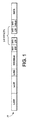
図1の線図は、物理層コンバージェンスプロトコル(PLCP)データ単位(PPDU10)を例示する。これは、IEEE802.11規格のもとで画定される基本的な物理層送信フレームを代表すると理解される。上述したように、802.11acのようなごく最近のWiFi規格は、802.11acが基礎とする初期の802.11a及び802.11n規格と同様、データが等間隔のサブキャリアにおいて送信される直交周波数分割マルチプレクシングを利用する。サブキャリアの数は帯域幅に大きく依存し、20MHz帯域幅のための64サブキャリアから、160MHz帯域幅のための512サブキャリアまでばらつき得る。初期の802.11a及び802.11n規格のもとで動作するレガシーデバイスと共存するべく、超高スループット(VHT)デバイスが必要とされる。したがって、VHTデバイスは、すべての802.11デバイスがパケットと同期し得るように、各20MHzサブ帯域において同じプリアンブルを送信する。 The diagram of FIG. 1 illustrates physical layer convergence protocol (PLCP) data units (PPDU 10). This is understood to represent a basic physical layer transmission frame defined under the IEEE 802.11 standard. As noted above, most recent WiFi standards such as 802.11ac, like the early 802.11a and 802.11n standards on which 802.11ac is based, are orthogonal with data transmitted on equally spaced subcarriers. Use frequency division multiplexing. The number of subcarriers is highly dependent on bandwidth and can vary from 64 subcarriers for a 20 MHz bandwidth to 512 subcarriers for a 160 MHz bandwidth. Very high throughput (VHT) devices are required to coexist with legacy devices operating under the early 802.11a and 802.11n standards. Thus, the VHT device transmits the same preamble in each 20 MHz subband so that all 802.11 devices can be synchronized with the packet.
さらに詳しくは、混合フォーマットPPDU10が、2シンボルのレガシーショートトレーニングフィールド(L−STF)と、やはり2シンボルのレガシーロングトレーニングフィールド(L−LTF)とを含む。これらは、以前の規格との下位互換性を目的として使用され、さもなくばRF電力増幅器の効率を低減させるピーク対平均電力比(PAPR)の効果を緩和するべく、各20MHzサブ帯域のために位相回転によって複製される。これらのトレーニングフィールドの後には、バイナリ位相シフトキーイング(BPSK)によって送信される1シンボルのレガシー信号フィールド(L−SIG)が続く。 More specifically, the mixed format PPDU 10 includes a 2-symbol legacy short training field (L-STF) and a 2-symbol legacy long training field (L-LTF). These are used for backward compatibility with previous standards, and for each 20 MHz subband to mitigate the effects of peak-to-average power ratio (PAPR) that would otherwise reduce the efficiency of the RF power amplifier. Replicated by phase rotation. These training fields are followed by a 1-symbol legacy signal field (L-SIG) transmitted by binary phase shift keying (BPSK).
VHT送信に固有のフィールドは、802.11acのPPDU10の一部でもあり、2シンボルのVHT−SIG−Aフィールドを含む。これは、受信器がどのようにして後続パケットを解釈するべきかを通信し、帯域幅、MIMOストリームの数、使用される空間・時間ブロックコード、ガードインターバル等を特定する。加えて、MIMO動作に対する利得制御推定を改善するために使用される1シンボルのVHTショートトレーニングフィールド(VHT−STF)と、それぞれ1シンボルの可変数(1、2、4、6又は8つ)のVHTロングトレーニングフィールド(VHT−LTF)とが存在する。ペイロードデータを詳述するVHT−SIG−Bフィールドが存在する。これは、マルチユーザーモードのためのデータ長及び変調コーディング方式を含む。これらのフィールドに引き続くのがDATAデータフィールドである。 A field specific to VHT transmission is also part of the 802.11ac PPDU 10 and includes a 2 symbol VHT-SIG-A field. It communicates how the receiver should interpret subsequent packets and specifies bandwidth, number of MIMO streams, space / time block code used, guard interval, etc. In addition, one symbol of VHT short training field (VHT-STF) used to improve gain control estimation for MIMO operation, and a variable number (1, 2, 4, 6, or 8) of 1 symbol each. There is a VHT Long Training Field (VHT-LTF). There is a VHT-SIG-B field detailing the payload data. This includes data length and modulation coding scheme for multi-user mode. Following these fields is the DATA data field.
ここで図2の線図を参照すると、OFDMトレーニングシーケンス構造12には、t1からt10までのショートトレーニングシンボルと、ガードインターバルGI2によって区切られたT1及びT2のロングトレーニングシンボルとが含まれる。トレーニングシンボルの第1セット12aが、信号検出、自動利得制御及びダイバーシティ選択を目的として使用される一方、トレーニングシンボルの第2セット12bは、受信器ノードにおける粗い周波数オフセット推定とタイミング同期とを目的として使用される。各シンボルは、16サンプル長すなわち0.8μsである。第3セット12c内にあるロングトレーニングシンボルは、細かい周波数オフセット推定とチャンネル係数推定とを目的として使用される。ロングトレーニングシンボルの後には、それぞれがガードインターバルGIによって区切られたSIGNAL及びDATAフィールドが続く。
Referring now to the diagram of FIG. 2, the OFDM
位相トラッキングは、WiFi実装にとっての中心的要求である。OFDM(直交周波数分割マルチプレクシング)が多数のサブキャリアからなり、各サブキャリアがBPSK、QPSK及びQAMのような振幅及び位相変調を備えるからである。ここで図3の線図を参照すると、受信チェーンにおいてPLL(位相ロックループ)周波数を設定するべく、粗い周波数オフセット推定が、第2シンボルにおいて復調器により使用される。周波数検出器が信号の位相検出に基づくことが理解される。復調器における細かい周波数オフセット推定が、第4シンボルの終わりまでにPLLの正確な周波数を設定する。基準位相はΔΦ=0に設定される。各連続シンボルがΔΦ=0と対比されるので、各連続シンボルは、周波数オフセットがPLLにおいて確立される箇所である位相Φ1を基準とする位相誤差ΔΦnを有すると理解される。かかる誤差の合計が、送信チェーンに存在し得る他の振幅誤差を伴って、パケットバーストにわたる全体的なEVMをもたらすと理解される。この手法は、業界においてプリアンブルトラッキングと称され、ペイロードトラッキング手法に対し、必要なプロセッサリソースが最小限になりかつWiFiシステムの電流消費が低減されるとの利点を有すると理解される。 Phase tracking is a central requirement for WiFi implementations. This is because OFDM (Orthogonal Frequency Division Multiplexing) consists of a large number of subcarriers, and each subcarrier has amplitude and phase modulation such as BPSK, QPSK and QAM. Referring now to the diagram of FIG. 3, a coarse frequency offset estimate is used by the demodulator in the second symbol to set the PLL (Phase Locked Loop) frequency in the receive chain. It will be appreciated that the frequency detector is based on the phase detection of the signal. A fine frequency offset estimate at the demodulator sets the exact frequency of the PLL by the end of the fourth symbol. The reference phase is set to ΔΦ = 0. Since each successive symbol is contrasted with ΔΦ = 0, each successive symbol is understood to have a phase error ΔΦn relative to the phase Φ1 where the frequency offset is established in the PLL. It is understood that the sum of such errors results in an overall EVM over the packet burst, with other amplitude errors that may be present in the transmit chain. This approach, referred to in the industry as preamble tracking, is understood to have the advantage over the payload tracking approach that the required processor resources are minimized and the current consumption of the WiFi system is reduced.
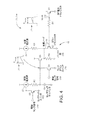
本開示の様々な実施形態は、プリアンブルトラッキングWiFiシステムにおいて動的EVMを最小限にすることに関する。図4の模式的な線図を参照すると、バイアス制御回路14aの第1実施形態が、トランジスタQ1によって代表されるRF電力増幅器段に接続されるように示される。この点で、バイアス制御回路14aはバイアス制御出力16を有すると理解される。トランジスタQ1のゲートは、RF電力増幅器入力に対応し、RF電力増幅器入力にはRF信号入力も接続される。 Various embodiments of the present disclosure relate to minimizing dynamic EVM in a preamble tracking WiFi system. Referring to the schematic diagram of FIG. 4, a first embodiment of bias control circuit 14a is shown connected to an RF power amplifier stage represented by transistor Q1. In this regard, it is understood that the bias control circuit 14 a has a bias control output 16. The gate of transistor Q1 corresponds to the RF power amplifier input, and an RF signal input is also connected to the RF power amplifier input.
RF電力増幅器、例えばトランジスタQ1は、ミラートランジスタQ2を含む電流ミラー回路18によるバイアスを受ける。ミラートランジスタQ2のゲート端子及びドレイン端子はRF電力増幅器の入力、具体的にはトランジスタQ1のゲート端子に接続される。抵抗器R1がトランジスタQ1及びQ2の各ゲート端子を相互接続し、RF信号入力をバイアス制御回路14からデカプリングすると理解される。したがって、抵抗器R1は大きな値を有する。ミラートランジスタQ2には、主要電流源20を介してバイアスがかけられ、主要電流源20は、抵抗器R2に直列するミラートランジスタQ2のドレインに接続される。主要電流源20は、RF信号送信バーストの間中、一定電流を生成すると理解される。 An RF power amplifier, eg, transistor Q1, is biased by a current mirror circuit 18 that includes a mirror transistor Q2. The gate terminal and drain terminal of the mirror transistor Q2 are connected to the input of the RF power amplifier, specifically to the gate terminal of the transistor Q1. It will be appreciated that resistor R1 interconnects the gate terminals of transistors Q1 and Q2 and decouples the RF signal input from bias control circuit 14. Therefore, resistor R1 has a large value. The mirror transistor Q2 is biased via the main current source 20, which is connected to the drain of the mirror transistor Q2 in series with the resistor R2. The main current source 20 is understood to generate a constant current throughout the RF signal transmission burst.
主要電流源20に加え、バイアス制御回路14の様々な実施形態も、補助電流源22に組み入れられると理解される。主要電流源20と同様、補助電流源22は、オンにされると一定電流を出力する。バイアス制御回路14はさらに、ランプアップスイッチ24、すなわち、補助電流源22を選択的にアクティブにするトランジスタQ3を含む。一般に制御信号と称される開始ランプ信号26により、トランジスタQ3はオン及びオフにされる。開始ランプ信号26は、RF信号送信バーストとともに、具体的にはその開始時に、オン又は高の状態に遷移すると理解される。トランジスタQ3がオンにされると、補助電流源22から抵抗器R3を経由するDC電流が、ランプアップキャパシタC1の充電を開始する。
In addition to the main current source 20, it is understood that various embodiments of the bias control circuit 14 are also incorporated into the auxiliary current source 22. As with the main current source 20, the auxiliary current source 22 outputs a constant current when turned on. The bias control circuit 14 further includes a transistor Q3 that selectively activates the ramp-up switch 24, ie, the auxiliary current source 22. Transistor Q3 is turned on and off by a
すなわち、図5に例示のように、補助電流源22の出力が、ランプアップスイッチ24によって制御されるとおりに、ランプアップキャパシタC1、ランプダウンスイッチ28及びバッファ段30に接続される。ランプダウンスイッチ28は、停止ランプ信号32によって選択的にアクティブにされ得るトランジスタQ4に対応する。一般に、開始ランプ信号26がアクティブになると、停止ランプ信号が非アクティブとなってトランジスタQ4がオフになる。
That is, as illustrated in FIG. 5, the output of the auxiliary current source 22 is connected to the ramp-up capacitor C <b> 1, the ramp-down switch 28 and the buffer stage 30 as controlled by the ramp-up switch 24. Ramp down switch 28 corresponds to
さらに詳細には、バッファ段30は、トランジスタQ5に基づくソースフォロワ(共通ドレイン段)として実装してよい。トランジスタQ5のゲート端子が入力に、ソース端子が出力に対応する。バッファ段30の入力、例えばトランジスタQ5のゲート端子における電圧は、プロット34に示されるように、RF信号送信バーストの持続時間にわたって線形依存性を有すると理解される。この電圧は、加算ノード36において主要電流源20からの電圧に加えられる。加算ノード36は、トランジスタQ5のソース端子、並びにミラートランジスタQ2のドレイン端子及びゲート端子に接続される(加算ノード)。主要電流源20からの一定DC電圧が、補助電流源22からのランプ電圧と一緒になって、プロット38に持続時間Tバーストとともに表されるバイアス信号をもたらす。様々な実施形態によれば、加算ノード36において主要電流源20から供給される電圧とともに線形的に増加する電圧の傾きが、RF信号送信バースト全体にわたってS21(利得)及びS21位相特性を補償すると理解される。したがって、全体的な動的EVMの最小化を達成することができる。 More specifically, the buffer stage 30 may be implemented as a source follower (common drain stage) based on the transistor Q5. The gate terminal of the transistor Q5 corresponds to the input, and the source terminal corresponds to the output. It is understood that the voltage at the input of buffer stage 30, for example the gate terminal of transistor Q5, has a linear dependence over the duration of the RF signal transmission burst, as shown in plot 34. This voltage is added to the voltage from the main current source 20 at the summing node 36. The addition node 36 is connected to the source terminal of the transistor Q5 and the drain terminal and gate terminal of the mirror transistor Q2 (addition node). A constant DC voltage from the main current source 20 along with the ramp voltage from the auxiliary current source 22 results in a bias signal represented in plot 38 with a duration T burst . According to various embodiments, it is understood that the slope of the voltage that increases linearly with the voltage supplied from the main current source 20 at the summing node 36 compensates for the S21 (gain) and S21 phase characteristics throughout the RF signal transmission burst. Is done. Therefore, overall dynamic EVM minimization can be achieved.
RF信号送信バーストの終わりに、開始ランプ信号26が非アクティブ又はオフにされることにより、補助電流源22がデカプリングされる。さらに、停止ランプ信号32がアクティブ又はオンにされることにより、ランプダウンスイッチ28例えばトランジスタQ4がアクティブにされる。ランプアップキャパシタC1に格納された残りの電圧は、グランドへの電流経路を与えるトランジスタQ4の小抵抗を介して放電されると理解される。
At the end of the RF signal transmission burst, the
第2実施形態のバイアス制御回路14bが、図6の模式的な線図に示される。再びであるが、バイアス制御回路14は、トランジスタQ1により表されるRF電力増幅器段に接続され、バイアス制御出力16を画定する。トランジスタQ1のゲートは、RF信号入力が接続されたRF電力増幅器入力に対応する。
The bias control circuit 14b of the second embodiment is shown in the schematic diagram of FIG. Again, the bias control circuit 14 is connected to the RF power amplifier stage represented by
第1実施形態14aと同様、RF電力増幅器、例えばトランジスタQ1は、ミラートランジスタQ2を含む電流ミラー回路18によってバイアスがかけられる。ミラートランジスタQ2のゲート端子及びドレイン端子は、RF電力増幅器の入力に、具体的にはトランジスタQ1のゲート端子に接続される。抵抗器R1がトランジスタQ1及びQ2の各ゲート端子を相互接続し、RF信号入力をバイアス制御回路14からデカプリングする。ミラートランジスタQ2には、主要電流源20によってバイアスがかけられる。主要電流源20は、抵抗器R2と直列となるようにミラートランジスタQ2のドレインに接続される。主要電流源20は、RF信号送信バースト中に一定電流を生成する。
Similar to the first embodiment 14a, the RF power amplifier, eg, transistor Q1, is biased by a current mirror circuit 18 including a mirror transistor Q2. The gate terminal and drain terminal of the mirror transistor Q2 are connected to the input of the RF power amplifier, specifically to the gate terminal of the transistor Q1.
バイアス制御回路14bの第2実施形態はまた、オンになると一定電流を出力する補助電流源22を組み入れる。再びであるが、ランプアップスイッチ24(トランジスタQ3)が、補助電流源22を選択的にアクティブにする。一般に制御信号と称される開始ランプ信号26により、トランジスタQ3がオン及びオフにされる。第2実施形態において、開始ランプ信号26は、プロット40に示されるパルスであり、RF信号送信バーストの開始時に生成される。トランジスタQ3がオンになる一方、補助電流源22からのDC電流は抵抗器R3を介してランプアップキャパシタC1と特定の電圧レベルまで充電する。開始ランプ信号26のパルス持続時間は短いので、充電時間も短い。これは、信号シンボル持続時間未満と理解され、数ナノ秒の長さにすぎない。
The second embodiment of the bias control circuit 14b also incorporates an auxiliary current source 22 that outputs a constant current when turned on. Again, the ramp up switch 24 (transistor Q3) selectively activates the auxiliary current source 22. Transistor Q3 is turned on and off by a
ひとたび開始ランプ信号26がゼロに戻ると、ランプアップキャパシタC1は抵抗器R5を介して放電を行う。抵抗器R5は、補助電流源22の出力及びランプアップキャパシタC1にも接続される。すなわち、(ランプアップキャパシタC1、抵抗器R5及び補助電流源22が接続された)ノード42には、RF信号送信の最小バースト幅未満となる時間フレームの中に指数関数的に減衰する電圧が存在する。様々な実施形態によれば、この持続時間は数十マイクロ秒と理解される。一例のプロット44は、ランプアップキャパシタC1の、漸次的な放電が引き続いて生じる初期高速ランプアップ充電を示す。
Once
バイアス制御回路14bの第2実施形態はインバータ段46を組み入れる。インバータ段46への入力は、ノード42、例えばランプアップキャパシタC1、補助電流源22の出力、及び抵抗器R5に接続される。インバータ段46は、その出力において、プロット48に示されるように、電圧信号を反転させる。ここで、急激な電圧降下が存在し、その後、持続時間の引き延ばしを目的とした増加が引き続いて生じる。この電圧は、バッファ段30への入力となる。これは、加算ノード36において主要電流源20による一定電圧信号出力と組み合わせられる。プロット50は、この組み合わせに従う典型的なバイアス制御電圧信号を例示する。
The second embodiment of the bias control circuit 14b incorporates an inverter stage 46. The input to inverter stage 46 is connected to node 42, such as ramp-up capacitor C1, the output of auxiliary current source 22, and resistor R5. Inverter stage 46 inverts the voltage signal at its output , as shown in plot 48. Here, there is an abrupt voltage drop, followed by an increase aimed at extending the duration. This voltage is input to the buffer stage 30. This is combined with a constant voltage signal output by the main current source 20 at the summing node 36. Plot 50 illustrates a typical bias control voltage signal according to this combination.
明らかに考えられることだが、指数関数的に増加する電圧の傾きは、ランプアップキャパシタC1及び/又は抵抗器R5の値を変更することによって調整できる。さらに、ランプアップキャパシタC1に充電される初期電圧レベルは、加算ノード36において主要電流源20が与える電圧とともに、RF信号送信バースト全体にわたって利得及び位相特性を補償する結果をもたらす。したがって、全体的な動的EVMを最小限にできる。ランプアップ時間は、動的EVMが、RF信号送信バースト開始時におけるDC電圧の短いスパイクによって劣化されないように選択される。考慮された実施形態では、連続シンボルの位相が、細かい周波数オフセット推定の間、補償された位相と対比されることに起因して最初のいくつかの送信されたシンボルが歪んだにもかかわらず、RF信号送信バースト中の全体的なEVMは最小限になると理解される。
Obviously, the exponentially increasing voltage slope can be adjusted by changing the value of the ramp-up capacitor C1 and / or the resistor R5. In addition, the initial voltage level charged to the ramp-up capacitor C1 , along with the voltage provided by the main current source 20 at the summing node 36, results in compensating gain and phase characteristics throughout the RF signal transmission burst. Thus, overall dynamic EVM can be minimized. The ramp-up time is selected so that the dynamic EVM is not degraded by a short spike in DC voltage at the beginning of the RF signal transmission burst. In the considered embodiment, despite the fact that the first few transmitted symbols are distorted due to the phase of successive symbols being contrasted with the compensated phase during fine frequency offset estimation. It is understood that the overall EVM during the RF signal transmission burst is minimized.
ここで図7の模式的な線図を参照すると、出力52がバイアス電流源として様々なRF電力増幅器に同様に接続可能なバイアス制御回路14cのさらなる第3実施形態が存在する。バイアス制御回路14cは、3つの出力ノードに安定電流を与えるバンドギャップ基準回路54に接続されてよい。第1電流出力I1が、グランドに結びつけられた抵抗器R1に接続され、第2電流出力I2が、やはりグランドに結びつけられた抵抗器R2に接続される。したがって、抵抗器R1及びR2は、第1及び第2電流出力I1及びI2それぞれと一緒になって、V1及びV2を基準電圧として画定する。 Referring now to the schematic diagram of FIG. 7, there is a further third embodiment of a bias control circuit 14c in which the output 52 can be similarly connected to various RF power amplifiers as a bias current source. The bias control circuit 14c may be connected to a bandgap reference circuit 54 that provides stable currents to the three output nodes. The first current output I1 is connected to a resistor R1 tied to ground, and the second current output I2 is connected to a resistor R2 also tied to ground. Thus, resistors R1 and R2 together with the first and second current outputs I1 and I2, respectively, define V1 and V2 as reference voltages.
バイアス制御回路14cはまた、基準電圧V1に結びつけられた第1投端子56aと、基準電圧V2に結びつけられた第2投端子56bとを備えたスイッチ55も含む。スイッチ55はさらに、イネーブルライン入力60a及び/又は逆イネーブルライン入力60bに応じて第1及び第2投端子56a、56bの一方に選択的に接続される極端子58も含む。極端子58は、抵抗器R及びキャパシタCによって画定されたランプRCネットワーク62に接続される。様々な実施形態によれば、ランプRCネットワーク62は、持続時間が変化するRF送信バーストにおける動的EVM障害を補償するべく、基準電圧V1からV2までランプするための時定数を設定する。
The bias control circuit 14c also includes a switch 55 having a
演算増幅器64が、第1差動入力66a、第2差動入力66b及び演算増幅器出力68を備える。バンドギャップ基準回路54はまた、演算増幅器64に安定電流を与える。
The
ランプRCネットワーク62が第1差動入力66aに接続される一方、演算増幅器出力68は第2差動入力66bへとフィードバックされる。具体的には、演算増幅器出力68が、随意的ではあるが、PMOS型が好ましい出力トランジスタ70のゲートに接続される。出力トランジスタ70のドレイン端子は、抵抗器R3及びR4により形成された抵抗性分割器からなるフィードバックネットワーク72に接続される。抵抗器R3及びR4間の接合部が、第2差動入力66bに接続される。さらに、出力トランジスタ70のドレイン端子が出力52に対応すると理解される。出力52における電圧レベルは、フィードバックネットワーク72、出力トランジスタ70及び演算増幅器64によって設定される。
The lamp RC network 62 is connected to the first differential input 66a, while the operational amplifier output 68 is fed back to the second differential input 66b. Specifically, operational amplifier output 68 is optionally connected to the gate of output transistor 70, which is preferably a PMOS type. The drain terminal of the output transistor 70 is connected to a feedback network 72 consisting of a resistive divider formed by resistors R3 and R4. The junction between resistors R3 and R4 is connected to the second differential input 66b. It is further understood that the drain terminal of the output transistor 70 corresponds to the output 52. The voltage level at output 52 is set by feedback network 72, output transistor 70 and
上述のように、出力52は、RF電力増幅器トランジスタ段に、さらに詳しくは、かかるトランジスタのドレイン端子に接続される。多段電力増幅器において、バイアス制御回路14cの出力52は、電流の消費が最小量の第1段に接続されてよいが、出力52が任意の他の段に接続され、最終段に限られなくてよいことも考えられる。 As described above, the output 52 is connected to the RF power amplifier transistor stage, and more particularly to the drain terminal of such transistor. In the multistage power amplifier, the output 52 of the bias control circuit 14c may be connected to the first stage that consumes a minimum amount of current, but the output 52 is connected to any other stage and is not limited to the final stage. Good things are also possible.
図8A〜8Cのグラフを参照すると、イネーブルライン入力60、同じ持続時間中に得られた基準電圧Vref、及び出力52からの出力電圧を示す様々なタイミング図が考慮される。特に、図8Aは、イネーブルライン入力60をプロットする。時間T1において「高」となり、RF送信バーストの持続時間中、高が維持される。図8Bは、演算増幅器64への基準電圧入力が最初に電圧レベルV1から開始し、時間T1になって初めてイネーブルライン入力60が「高」に遷移することを示す。ここで、基準電圧入力は、時間T1から時間T1プラスRC時定数までに電圧レベルV2へと遷移する。ひとたびイネーブルライン入力60がゼロに戻るように遷移すると、基準電圧入力は電圧レベルV1へと遷移する。最後に、図8Cのプロットは、V1(R3+R4)/R4又はV2(R3+R4)/R4として定義される出力52の出力電圧を示す。すなわち、イネーブルライン入力60が低の場合、出力電圧は基準電圧V1及びフィードバックネットワーク72の関数となる一方、イネーブルライン入力60が高の場合、出力電圧は基準電圧V2及びフィードバックネットワーク72の関数となる。
Referring to the graphs of FIGS. 8A-8C, various timing diagrams showing the enable line input 60, the reference voltage Vref obtained during the same duration, and the output voltage from output 52 are considered. In particular, FIG. 8A plots enable line input 60. It goes “high” at time T1, and remains high for the duration of the RF transmit burst. FIG. 8B shows that the reference line input to the
ランプRCネットワーク62の抵抗器R及びキャパシタC、並びにフィードバックネットワーク72の抵抗器R3及びR4を含む様々なコンポーネントが一つのコンポーネントとして描かれているにもかかわらず、当業者には、かかるコンポーネントを画定するべく複数のコンポーネントを組み合わせ得ることがわかる。さらに、バイアス制御回路14の構成及び配列が考慮されてきたが、考えられる動的EVM最小化の目的を達成するための当該コンポーネントの特定値は、当業者の視野内にある。 Despite the various components depicted as one component, including resistor R and capacitor C of lamp RC network 62 and resistor R3 and R4 of feedback network 72, those skilled in the art will define such components. It can be seen that a plurality of components can be combined as much as possible. Further, although the configuration and arrangement of the bias control circuit 14 has been considered, specific values of the component to achieve the possible dynamic EVM minimization objectives are within the purview of those skilled in the art.
図9のグラフは、バイアス制御回路14cのシミュレートされた過渡応答を経時的にプロットする。異なるコンポーネント値に対し、第1領域74が出力初期電圧レベルに関する一方、第2領域76は出力最終電圧レベルに関する。 The graph of FIG. 9 plots the simulated transient response of the bias control circuit 14c over time. For different component values, the first region 74 relates to the output initial voltage level, while the second region 76 relates to the output final voltage level.
本開示の様々な実施形態によれば、基準電圧V1及びV2を、異なる周囲温度及びトランジスタ接合部温度に対して調整することができる。RF電力増幅器の位相特性及び振幅特性がこれらに依存し得るからである。図10のグラフは、周囲温度範囲にわたる補償特性を示す。ここで、第1セットのプロット78が、正の、負の、及び一定の温度プロファイルを伴う出力初期電圧レベルを示し、第2セットのプロット80が、正の、負の、及び一定の温度プロファイルを伴う出力最終電圧レベルを示す。この点において、バイアス制御回路14は、バンドギャップ基準回路54に接続可能な周囲温度電圧調整回路を含み得る。
According to various embodiments of the present disclosure, the reference voltages V1 and V2 can be adjusted for different ambient temperatures and transistor junction temperatures. This is because the phase characteristic and amplitude characteristic of the RF power amplifier can depend on them. The graph of FIG. 10 shows the compensation characteristics over the ambient temperature range. Here, a first set of plots 78 shows the output initial voltage level with positive, negative and constant temperature profiles, and a second set of
考慮されるのは、本開示のバイアス制御回路14が、RFトランジスタ段の動的切り替えの帰結である動的EVMを補償するべく、デジタル変調無線通信モダリティにおいて、及び異なる半導体技術に対して利用できることである。 It is contemplated that the bias control circuit 14 of the present disclosure can be utilized in digitally modulated wireless communication modalities and for different semiconductor technologies to compensate for the dynamic EVM that results from dynamic switching of RF transistor stages. It is.
ここに示される詳細は、一例であって、電力増幅器の実施形態の例示による説明を目的とするにすぎず、原理及び概念的側面の最も有用かつ容易に理解される説明と思われるものを与える目的で提示される。この点において、必要以上に具体的に詳細を示す試みはなされていない。本説明を図面とともに読むことで、本開示のいくつかの形態をいかにして実際に具体化できるのかが当業者にとって明らかとなる。
The details presented herein are only examples and are intended for illustrative purposes only of embodiments of the power amplifier and provide what appears to be the most useful and easily understood description of the principles and conceptual aspects. Presented for the purpose. At this point, no attempt has been made to show more specific details than necessary. It will be apparent to those skilled in the art, upon reading this description in conjunction with the drawings, how some aspects of the present disclosure may actually be embodied.
Claims (20)
電力増幅器出力及びRF信号入力を含む電力増幅器と、
前記電力増幅器に選択的にバイアスをかける制御回路と
を含み、
前記制御回路は、
補助電流源と、
前記補助電流源に接続されたランプアップキャパシタと、
前記補助電流源に接続されたランプアップスイッチと、
出力と前記ランプアップキャパシタに接続された入力とを含むバッファと、
前記電力増幅器に接続された加算ノードにおいて前記バッファの出力に接続された主要電流源と
を含み、
前記ランプアップスイッチは、RF信号バーストに対応する制御信号に応答し、前記補助電流源を選択的にアクティブにして前記ランプアップキャパシタを充電し、
前記バッファの入力における電圧は、RF信号バースト持続時間にわたって線形依存性を有し、
前記主要電流源は前記RF信号バースト中に一定電流を生成するRF電力増幅器回路。 A radio frequency (RF) power amplifier circuit comprising:
A power amplifier including a power amplifier output and an RF signal input;
A control circuit for selectively biasing the power amplifier;
The control circuit includes:
An auxiliary current source;
A ramp-up capacitor connected to the auxiliary current source;
A ramp-up switch connected to the auxiliary current source;
A buffer including an output and an input connected to the ramp-up capacitor;
A main current source connected to the output of the buffer at a summing node connected to the power amplifier;
The ramp-up switch is responsive to a control signal corresponding to an RF signal burst to selectively activate the auxiliary current source to charge the ramp-up capacitor;
The voltage at the input of the buffer has a linear dependence over the RF signal burst duration;
An RF power amplifier circuit in which the main current source generates a constant current during the RF signal burst.
前記主要電流源によりバイアスをかけられて前記電力増幅器に接続されたミラートランジスタと
をさらに含み、
前記電力増幅器は、前記RFデカプリング抵抗器を経由して前記ミラートランジスタに接続された電力増幅器トランジスタを含む請求項1のRF電力増幅器回路。 An RF decoupling resistor;
A mirror transistor biased by the main current source and connected to the power amplifier;
2. The RF power amplifier circuit of claim 1, wherein the power amplifier includes a power amplifier transistor connected to the mirror transistor via the RF decoupling resistor.
前記電力増幅器トランジスタのゲート端子が前記RF信号入力と前記RFデカプリング抵抗器の第1端子とに接続され、
前記ミラートランジスタのゲート端子が、前記RFデカプリング抵抗器の第2端子と前記ミラートランジスタのドレイン端子とに接続される請求項2のRF電力増幅器回路。 The power amplifier transistor and the mirror transistor each include a gate terminal, a drain terminal and a source terminal,
A gate terminal of the power amplifier transistor is connected to the RF signal input and a first terminal of the RF decoupling resistor;
The RF power amplifier circuit according to claim 2, wherein a gate terminal of the mirror transistor is connected to a second terminal of the RF decoupling resistor and a drain terminal of the mirror transistor.
前記ランプダウンスイッチは、前記RF信号バーストの終わりに前記ランプアップキャパシタを放電するべく選択的にアクティブにされ、
前記ランプアップスイッチは、前記RF信号バーストの終わりに非アクティブにされる請求項1のRF電力増幅器回路。 The control circuit further includes a lamp down switch connected to the ramp up capacitor;
The ramp down switch is selectively activated to discharge the ramp up capacitor at the end of the RF signal burst;
The RF power amplifier circuit of claim 1, wherein the ramp-up switch is deactivated at the end of the RF signal burst.
前記ランプアップキャパシタに接続された入力と前記バッファに接続された出力とを含むインバータと
をさらに含み、
前記インバータの入力における電圧が、最小RF信号バースト持続時間未満の持続時間において指数関数的に減衰し、
前記インバータの出力における電圧が前記線形依存性に対応する傾きを有する請求項1のRF電力増幅器回路。 A capacitor discharge resistor connected to the ramp-up capacitor;
An inverter including an input connected to the ramp-up capacitor and an output connected to the buffer;
The voltage at the input of the inverter decays exponentially in a duration less than the minimum RF signal burst duration ;
The RF power amplifier circuit of claim 1, wherein the voltage at the output of the inverter has a slope corresponding to the linear dependence .
前記補助電流源入力に接続されたランプアップキャパシタと、
前記開始ランプ信号入力に接続されたランプアップスイッチトランジスタであって、前記補助電流源入力を前記ランプアップキャパシタに接続するべく前記開始ランプ信号入力によって選択的にアクティブにされるランプアップスイッチトランジスタと、
前記ランプアップキャパシタに接続された入力と加算ノードにおいて前記主要電流源入力に接続された出力を備えたバッファ段と、
前記回路出力に対応するゲート端子と前記加算ノードに及び前記ゲート端子に接続されたソース端子とを備えたミラートランジスタと
を含み、
前記バッファ段の入力における電圧は、RF信号バースト持続時間にわたって線形依存性を有するRF電力増幅器バイアス回路。 An RF power amplifier bias circuit with a start ramp signal input, a main current source input, an auxiliary current source input and a circuit output,
A ramp-up capacitor connected to the auxiliary current source input;
A ramp-up switch transistor connected to the start ramp signal input, the ramp-up switch transistor selectively activated by the start ramp signal input to connect the auxiliary current source input to the ramp-up capacitor;
A buffer stage with an input connected to the ramp-up capacitor and an output connected to the main current source input at a summing node;
Look including a mirror transistor having a source terminal connected to the summing node and the gate terminal and to the gate terminal corresponding to the circuit output,
The RF power amplifier bias circuit, wherein the voltage at the input of the buffer stage has a linear dependence over the RF signal burst duration .
前記ランプアップキャパシタに接続されたキャパシタ放電抵抗器と
をさらに含む請求項11のRF電力増幅器バイアス回路。 An inverter stage having an input connected to the ramp-up capacitor and an output connected to the input of the buffer stage;
The RF power amplifier bias circuit of claim 11, further comprising a capacitor discharge resistor connected to the ramp-up capacitor.
前記ランプアップスイッチトランジスタは、前記RF信号バーストの終わりに非アクティブにされる請求項11のRF電力増幅器バイアス回路。 A ramp-down switch connected to the ramp-up capacitor that is selectively activated to discharge the ramp-up capacitor at the end of an RF signal burst;
12. The RF power amplifier bias circuit of claim 11, wherein the ramp up switch transistor is deactivated at the end of the RF signal burst.
Applications Claiming Priority (5)
| Application Number | Priority Date | Filing Date | Title |
|---|---|---|---|
| US201462048737P | 2014-09-10 | 2014-09-10 | |
| US62/048,737 | 2014-09-10 | ||
| PCT/US2015/049501 WO2016040688A2 (en) | 2014-09-10 | 2015-09-10 | Complementary metal oxide semiconductor radio frequency power amplifiers with high linearity across a wide range of burst signals in wifi applications |
| US14/849,936 | 2015-09-10 | ||
| US14/849,936 US9806679B2 (en) | 2014-09-10 | 2015-09-10 | High-linearity CMOS WiFi RF power amplifiers in wide range of burst signals |
Related Child Applications (1)
| Application Number | Title | Priority Date | Filing Date |
|---|---|---|---|
| JP2019140621A Division JP2019220965A (en) | 2014-09-10 | 2019-07-31 | Radio frequency (rf) power amplifier biasing circuit |
Publications (3)
| Publication Number | Publication Date |
|---|---|
| JP2017528994A JP2017528994A (en) | 2017-09-28 |
| JP2017528994A5 JP2017528994A5 (en) | 2018-10-18 |
| JP6567655B2 true JP6567655B2 (en) | 2019-08-28 |
Family
ID=55438462
Family Applications (2)
| Application Number | Title | Priority Date | Filing Date |
|---|---|---|---|
| JP2017513200A Active JP6567655B2 (en) | 2014-09-10 | 2015-09-10 | Radio frequency (RF) power amplifier circuit and RF power amplifier bias circuit |
| JP2019140621A Pending JP2019220965A (en) | 2014-09-10 | 2019-07-31 | Radio frequency (rf) power amplifier biasing circuit |
Family Applications After (1)
| Application Number | Title | Priority Date | Filing Date |
|---|---|---|---|
| JP2019140621A Pending JP2019220965A (en) | 2014-09-10 | 2019-07-31 | Radio frequency (rf) power amplifier biasing circuit |
Country Status (5)
| Country | Link |
|---|---|
| US (3) | US9806679B2 (en) |
| JP (2) | JP6567655B2 (en) |
| KR (1) | KR20170052639A (en) |
| CN (1) | CN106797204B (en) |
| WO (1) | WO2016040688A2 (en) |
Families Citing this family (26)
| Publication number | Priority date | Publication date | Assignee | Title |
|---|---|---|---|---|
| CN102984630B (en) | 2011-09-06 | 2015-12-02 | 昂宝电子(上海)有限公司 | For reducing the system and method for distortion in audio amplifier system |
| CN103441739B (en) | 2013-08-21 | 2015-04-22 | 昂宝电子(上海)有限公司 | Amplification system with one or more channels and amplification method |
| US9685919B2 (en) | 2013-08-21 | 2017-06-20 | On-Bright Electronics (Shanghai) Co., Ltd. | Amplification systems and methods with output regulation |
| US11201595B2 (en) * | 2015-11-24 | 2021-12-14 | Skyworks Solutions, Inc. | Cascode power amplifier with switchable output matching network |
| US9923529B2 (en) * | 2016-02-03 | 2018-03-20 | Samsung Electronics Co., Ltd | Customizable ramp-up and ramp-down amplitude profiles for a digital power amplifier (DPA) based transmitter |
| CN108123688B (en) * | 2016-11-28 | 2021-06-18 | 立积电子股份有限公司 | Boost circuit for power amplifier |
| US10014834B1 (en) * | 2016-12-29 | 2018-07-03 | STMicroelectronics (Alps) SAS | Differential sensing circuit of a floating voltage source |
| JP2018152714A (en) * | 2017-03-13 | 2018-09-27 | 株式会社村田製作所 | Power Amplifier Module |
| US10958222B2 (en) | 2018-06-15 | 2021-03-23 | Richwave Technology Corp. | Bias circuit |
| US10680564B2 (en) * | 2018-07-23 | 2020-06-09 | Analog Devices Global Unlimited Company | Bias circuit for high efficiency complimentary metal oxide semiconductor (CMOS) power amplifiers |
| KR102127808B1 (en) * | 2018-08-09 | 2020-06-29 | 삼성전기주식회사 | Power amplifier device with improved response speed |
| US10879853B2 (en) * | 2018-08-16 | 2020-12-29 | Samsung Electro-Mechanics Co., Ltd. | Bias circuit and power amplifier for improving linearity |
| US10742173B2 (en) * | 2018-09-24 | 2020-08-11 | Nxp Usa, Inc. | Systems and methods for fast switching time division duplex operation of power amplifiers |
| US11190152B2 (en) | 2018-11-15 | 2021-11-30 | Berex, Inc. | Control circuit for a radio frequency power amplifier |
| CN109450392A (en) * | 2018-12-27 | 2019-03-08 | 苏州英诺迅科技股份有限公司 | A kind of distribution emitter following amplifier |
| US11082021B2 (en) | 2019-03-06 | 2021-08-03 | Skyworks Solutions, Inc. | Advanced gain shaping for envelope tracking power amplifiers |
| TWI710210B (en) | 2019-06-13 | 2020-11-11 | 立積電子股份有限公司 | Bias device |
| WO2021061851A1 (en) | 2019-09-27 | 2021-04-01 | Skyworks Solutions, Inc. | Power amplifier bias modulation for low bandwidth envelope tracking |
| CN110753331B (en) * | 2019-10-18 | 2021-05-25 | 珠海格力电器股份有限公司 | Data transmission method, system, storage medium and networking device |
| US11482975B2 (en) | 2020-06-05 | 2022-10-25 | Skyworks Solutions, Inc. | Power amplifiers with adaptive bias for envelope tracking applications |
| US11855595B2 (en) | 2020-06-05 | 2023-12-26 | Skyworks Solutions, Inc. | Composite cascode power amplifiers for envelope tracking applications |
| CN111756375B (en) * | 2020-06-24 | 2023-08-04 | 成都华微电子科技股份有限公司 | High-linearity low-voltage input buffer circuit |
| US11437992B2 (en) | 2020-07-30 | 2022-09-06 | Mobix Labs, Inc. | Low-loss mm-wave CMOS resonant switch |
| CN113783540B (en) * | 2021-08-17 | 2022-09-23 | 深圳飞骧科技股份有限公司 | Power amplifier circuit and bias circuit thereof |
| TWI779839B (en) * | 2021-09-16 | 2022-10-01 | 威鋒電子股份有限公司 | Voltage comparator and operation method thereof |
| CN117498808B (en) * | 2023-12-29 | 2024-03-15 | 苏州悉芯射频微电子有限公司 | Circuit and method for improving performance of radio frequency power amplifier |
Family Cites Families (17)
| Publication number | Priority date | Publication date | Assignee | Title |
|---|---|---|---|---|
| JPS6091701A (en) * | 1983-10-25 | 1985-05-23 | Rohm Co Ltd | Amplifier circuit |
| US6639470B1 (en) * | 2000-10-06 | 2003-10-28 | Skyworks Solutions, Inc. | Constant current biasing circuit for linear power amplifiers |
| US6566944B1 (en) * | 2002-02-21 | 2003-05-20 | Ericsson Inc. | Current modulator with dynamic amplifier impedance compensation |
| US7268990B1 (en) * | 2003-05-15 | 2007-09-11 | Marvell International Ltd. | Power amplifier protection |
| US7443426B2 (en) | 2004-02-13 | 2008-10-28 | Canon Kabushiki Kaisha | Image capturing system and control method of the same |
| US7489183B2 (en) * | 2004-12-08 | 2009-02-10 | Triquint Semiconductor, Inc. | Bias control system for a power amplifier |
| JP4791271B2 (en) * | 2006-06-28 | 2011-10-12 | 富士通株式会社 | Amplifier control device |
| US7532066B1 (en) * | 2007-08-10 | 2009-05-12 | Triquinto Semiconductor, Inc. | Bias network with stable transient response |
| JP5136834B2 (en) * | 2007-10-16 | 2013-02-06 | 株式会社村田製作所 | RF power amplifier and power supply circuit for controlling power supply voltage of RF power amplifier |
| JP5194760B2 (en) * | 2007-12-14 | 2013-05-08 | 株式会社リコー | Constant voltage circuit |
| JP2009200770A (en) * | 2008-02-21 | 2009-09-03 | Sharp Corp | Power amplifier |
| JP4901804B2 (en) * | 2008-05-19 | 2012-03-21 | シャープ株式会社 | High frequency power amplifier |
| US20100198420A1 (en) * | 2009-02-03 | 2010-08-05 | Optisolar, Inc. | Dynamic management of power production in a power system subject to weather-related factors |
| KR101670994B1 (en) * | 2009-04-27 | 2016-11-01 | 페어차일드코리아반도체 주식회사 | Power factor correction circuit and driving method thereof |
| US8260224B2 (en) * | 2009-12-02 | 2012-09-04 | Sige Semiconductor Inc. | System and method of prebias for rapid power amplifier response correction |
| KR101300324B1 (en) | 2011-11-22 | 2013-08-28 | 삼성전기주식회사 | Power amplfier |
| US9154090B2 (en) * | 2012-05-17 | 2015-10-06 | Microsemi Corporation | Integrated start-up bias boost for dynamic error vector magnitude enhancement |
-
2015
- 2015-09-10 CN CN201580054995.2A patent/CN106797204B/en active Active
- 2015-09-10 WO PCT/US2015/049501 patent/WO2016040688A2/en active Application Filing
- 2015-09-10 KR KR1020177009429A patent/KR20170052639A/en unknown
- 2015-09-10 US US14/849,936 patent/US9806679B2/en active Active
- 2015-09-10 JP JP2017513200A patent/JP6567655B2/en active Active
-
2017
- 2017-09-29 US US15/720,335 patent/US10320344B2/en active Active
-
2019
- 2019-05-09 US US16/408,139 patent/US20190273473A1/en not_active Abandoned
- 2019-07-31 JP JP2019140621A patent/JP2019220965A/en active Pending
Also Published As
| Publication number | Publication date |
|---|---|
| US20160072444A1 (en) | 2016-03-10 |
| US10320344B2 (en) | 2019-06-11 |
| KR20170052639A (en) | 2017-05-12 |
| US20190273473A1 (en) | 2019-09-05 |
| US9806679B2 (en) | 2017-10-31 |
| WO2016040688A3 (en) | 2016-09-09 |
| JP2019220965A (en) | 2019-12-26 |
| CN106797204A (en) | 2017-05-31 |
| JP2017528994A (en) | 2017-09-28 |
| WO2016040688A2 (en) | 2016-03-17 |
| CN106797204B (en) | 2021-03-16 |
| US20180097482A1 (en) | 2018-04-05 |
Similar Documents
| Publication | Publication Date | Title |
|---|---|---|
| JP6567655B2 (en) | Radio frequency (RF) power amplifier circuit and RF power amplifier bias circuit | |
| Lu et al. | A 24.7 dBm all-digital RF transmitter for multimode broadband applications in 40nm CMOS | |
| US7116947B2 (en) | Transmitter | |
| US7116946B2 (en) | Transmitter | |
| US20140111279A1 (en) | Envelope tracking distributed amplifier | |
| CN102057568A (en) | Methods and systems of AGC and DC calibration for OFDM/OFDMA systems | |
| KR20100102167A (en) | Imbalance compensation for direct conversion communication systems | |
| US10972138B2 (en) | Technique for generating a protocol data unit signal | |
| US20190158041A1 (en) | Amplifier linearizer with wide bandwidth | |
| Varahram et al. | Power efficiency in broadband wireless communications | |
| US11595003B2 (en) | Programmable driver for frequency mixer | |
| Hasegawa et al. | Static sequence assisted out-of-band power suppression for DFT-s-OFDM | |
| CN109478870B (en) | Envelope tracking with selection between boost and battery power supplies | |
| JP2006157435A (en) | Distortion compensating circuit, power amplifier using the same and communications apparatus having the power amplifier | |
| US10979002B2 (en) | Current-limiting circuit for a power amplifier | |
| US20220416804A1 (en) | Digital amplitude tracking current steering digital-to-analog converter | |
| US9813025B2 (en) | Apparatus and method for power supply modulation | |
| Sen et al. | Concurrent PAR and power amplifier adaptation for power efficient operation of WiMAX OFDM transmitters | |
| WO2023188161A1 (en) | Wireless communication device and wireless communication method | |
| US9270313B2 (en) | Wireless receiver and method for wireless reception | |
| US20230085587A1 (en) | Dynamic envelope-tracking supply rail voltage setting | |
| US20220231641A1 (en) | Load-adaptive power amplifier | |
| Singh et al. | EFFECT OF HPA BACK-OFF AND FILTER LENGTH ON 256QAM | |
| Gao et al. | Bandwidth-Efficient Modulation With OFDM | |
| KR20240045227A (en) | Output common mode control for dynamic amplifiers |
Legal Events
| Date | Code | Title | Description |
|---|---|---|---|
| A521 | Request for written amendment filed |
Free format text: JAPANESE INTERMEDIATE CODE: A523 Effective date: 20180910 |
|
| A621 | Written request for application examination |
Free format text: JAPANESE INTERMEDIATE CODE: A621 Effective date: 20180910 |
|
| A871 | Explanation of circumstances concerning accelerated examination |
Free format text: JAPANESE INTERMEDIATE CODE: A871 Effective date: 20180910 |
|
| A977 | Report on retrieval |
Free format text: JAPANESE INTERMEDIATE CODE: A971007 Effective date: 20181220 |
|
| A975 | Report on accelerated examination |
Free format text: JAPANESE INTERMEDIATE CODE: A971005 Effective date: 20181226 |
|
| A131 | Notification of reasons for refusal |
Free format text: JAPANESE INTERMEDIATE CODE: A131 Effective date: 20190122 |
|
| A521 | Request for written amendment filed |
Free format text: JAPANESE INTERMEDIATE CODE: A523 Effective date: 20190419 |
|
| TRDD | Decision of grant or rejection written | ||
| A01 | Written decision to grant a patent or to grant a registration (utility model) |
Free format text: JAPANESE INTERMEDIATE CODE: A01 Effective date: 20190702 |
|
| A61 | First payment of annual fees (during grant procedure) |
Free format text: JAPANESE INTERMEDIATE CODE: A61 Effective date: 20190731 |
|
| R150 | Certificate of patent or registration of utility model |
Ref document number: 6567655 Country of ref document: JP Free format text: JAPANESE INTERMEDIATE CODE: R150 |
|
| R250 | Receipt of annual fees |
Free format text: JAPANESE INTERMEDIATE CODE: R250 |
|
| R250 | Receipt of annual fees |
Free format text: JAPANESE INTERMEDIATE CODE: R250 |