JP6531901B2 - Lighting device and projector - Google Patents

Lighting device and projector Download PDF

Info

Publication number
JP6531901B2
JP6531901B2 JP2015104221A JP2015104221A JP6531901B2 JP 6531901 B2 JP6531901 B2 JP 6531901B2 JP 2015104221 A JP2015104221 A JP 2015104221A JP 2015104221 A JP2015104221 A JP 2015104221A JP 6531901 B2 JP6531901 B2 JP 6531901B2
Authority
JP
Japan
Prior art keywords
light
unit
flux
optical
light flux
Prior art date
Legal status (The legal status is an assumption and is not a legal conclusion. Google has not performed a legal analysis and makes no representation as to the accuracy of the status listed.)
Expired - Fee Related
Application number
JP2015104221A
Other languages
Japanese (ja)
Other versions
JP2016218303A (en
Inventor
伊藤 嘉高
嘉高 伊藤
Current Assignee (The listed assignees may be inaccurate. Google has not performed a legal analysis and makes no representation or warranty as to the accuracy of the list.)
Seiko Epson Corp
Original Assignee
Seiko Epson Corp
Priority date (The priority date is an assumption and is not a legal conclusion. Google has not performed a legal analysis and makes no representation as to the accuracy of the date listed.)
Filing date
Publication date
Application filed by Seiko Epson Corp filed Critical Seiko Epson Corp
Priority to JP2015104221A priority Critical patent/JP6531901B2/en
Publication of JP2016218303A publication Critical patent/JP2016218303A/en
Application granted granted Critical
Publication of JP6531901B2 publication Critical patent/JP6531901B2/en
Expired - Fee Related legal-status Critical Current
Anticipated expiration legal-status Critical

Links

Images

Landscapes

  • Optical Elements Other Than Lenses (AREA)
  • Projection Apparatus (AREA)
  • Non-Portable Lighting Devices Or Systems Thereof (AREA)
  • Transforming Electric Information Into Light Information (AREA)

Description

本発明は、照明装置およびプロジェクターに関する。   The present invention relates to a lighting device and a projector.

プロジェクターは、照明装置から射出される光を光変調装置で画像情報に応じて変調し、得られた画像を投射装置によって拡大投射するものである。近年、このようなプロジェクターに用いられる照明装置の光源として、半導体レーザー(LD)などの半導体発光素子が注目されている。   The projector modulates the light emitted from the illumination device with the light modulation device according to the image information, and enlarges and projects the obtained image with the projection device. In recent years, semiconductor light emitting devices such as semiconductor lasers (LDs) have attracted attention as light sources of illumination devices used in such projectors.

高輝度化が要求されるプロジェクターに対して、半導体発光素子単体の光出力は十分でないため、このような照明装置では、一般的に、複数の半導体発光素子をアレイ化して用いる。   Since the light output of a single semiconductor light emitting element is not sufficient for a projector requiring high luminance, such a lighting device generally uses a plurality of semiconductor light emitting elements in an array.

例えば特許文献1には、基板の主面上に形成され、該基板の主面の面内方向と平行な方向に光を射出する複数の半導体レーザーと、複数の半導体レーザーの各々から射出された光を基板の主面から離れる方向に反射させる光学部材と、を備えた照明装置が開示されている。   For example, according to Patent Document 1, a plurality of semiconductor lasers formed on the main surface of a substrate and emitting light in a direction parallel to the in-plane direction of the main surface of the substrate and a plurality of semiconductor lasers are emitted. And an optical member for reflecting light in a direction away from the main surface of the substrate.

特開2010−45274号公報JP, 2010-45274, A

しかしながら、特許文献1の照明装置では、各半導体レーザーから射出された光の光軸間の距離が、発光素子の(光導波路の方向の)長さ分以上離れてしまう。したがって、特許文献1の照明装置をプロジェクターに用いた場合、エテンデュー(光源の発光面積と光源から射出される光の立体角との積)が大きくなってしまい光の利用効率が低下してしまう。   However, in the illumination device of Patent Document 1, the distance between the optical axes of the light emitted from the respective semiconductor lasers is separated by the length of the light emitting element (in the direction of the optical waveguide) or more. Therefore, when the lighting device of Patent Document 1 is used for a projector, the etendue (the product of the light emitting area of the light source and the solid angle of light emitted from the light source) becomes large, and the light utilization efficiency decreases.

本発明のいくつかの態様に係る目的の1つは、光の利用効率を高めることができる照明装置を提供することにある。また、本発明のいくつかの態様に係る目的の1つは、上記照明装置を含むプロジェクターを提供することにある。   One of the objects according to some aspects of the present invention is to provide a lighting device capable of enhancing the utilization efficiency of light. Another object of some aspects of the present invention is to provide a projector including the lighting device.

本発明に係る照明装置は、
第1の光束を射出する第1照明ユニットと、
第2の光束を射出する第2照明ユニットと、
前記第1の光束と前記第2の光束とを合成する光合成部と、
を含み、
前記第1照明ユニットおよび前記第2照明ユニットは、
基板と、
前記基板の第1面に実装され、かつ、前記第1面の面内方向に光を射出する複数の半導体発光素子と、
前記複数の半導体発光素子から射出された光の各々を、前記第1面から離れる方向に折り曲げる折り曲げ部と、
前記折り曲げ部によって折り曲げられた光の各々を平行化するコリメート部と、
前記コリメート部によって平行化された複数の光の光軸間の距離を短くする光学部と、を有する。
The lighting device according to the present invention is
A first lighting unit that emits a first light flux;
A second lighting unit that emits a second light flux;
A light combining unit that combines the first light beam and the second light beam;
Including
The first lighting unit and the second lighting unit are
A substrate,
A plurality of semiconductor light emitting elements mounted on the first surface of the substrate and emitting light in the in-plane direction of the first surface;
A bending portion which bends each of the light emitted from the plurality of semiconductor light emitting elements in a direction away from the first surface;
A collimating unit that collimates each of the light bent by the bending unit;
And an optical unit for shortening the distance between the optical axes of the plurality of lights collimated by the collimating unit.

このような照明装置では、第1照明ユニットおよび第2照明ユニットが平行化された光の光軸間の距離を短くする光学部を有し、第1照明ユニットおよび第2照明ユニットから射出された光束が光合成部で合成されるため、例えば各照明ユニットが光学部を有さない場合と比べて、光合成部で合成された合成光束の径(発光面積)を小さくすることができる。したがって、このような照明装置では、複数の半導体発光素子を用いて高出力化を図りつつ、エテンデューを小さくして光利用効率を高めることができる。   In such a lighting device, the first lighting unit and the second lighting unit have an optical unit that shortens the distance between the optical axes of the collimated light, and are emitted from the first lighting unit and the second lighting unit. Since the light fluxes are combined in the light combining section, the diameter (emission area) of the combined light flux combined in the light combining section can be reduced, for example, as compared to the case where each lighting unit does not have the optical section. Therefore, in such a lighting device, it is possible to reduce the etendue and enhance the light utilization efficiency while achieving high output by using a plurality of semiconductor light emitting elements.

本発明に係る照明装置において、
前記複数の半導体発光素子は、前記第1面に複数行かつ複数列に配置され、
前記第1の光束は、前記第1の光束の光軸と直交する平面内において複数行かつ複数列に配置された光で構成され、
前記第2の光束は、前記第2の光束の光軸と直交する平面内において複数行かつ複数列に配置された光で構成され、
前記光合成部は、前記第1の光束を構成する光の列と、前記第2の光束を構成する光の列とを、交互に配置してもよい。
In the lighting device according to the present invention,
The plurality of semiconductor light emitting devices are arranged in a plurality of rows and a plurality of columns on the first surface,
The first beam is composed of light arranged in a plurality of rows and a plurality of columns in a plane orthogonal to the optical axis of the first beam.
The second beam is composed of light arranged in a plurality of rows and a plurality of columns in a plane orthogonal to the optical axis of the second beam.
The light combining unit may alternately arrange a row of light forming the first light beam and a row of light forming the second light beam.

このような照明装置では、第1の光束を構成する光の列と第2の光束を構成する光の列とが交互に配置された合成光束を得ることができる。   In such an illumination device, it is possible to obtain a combined luminous flux in which the light trains constituting the first luminous flux and the light trains constituting the second luminous flux are alternately arranged.

本発明に係る照明装置において、
前記光合成部は、
第2面を有する第1プリズムと、
前記第2面と対向する第3面を有する第2プリズムと、
を有し、
前記第2面と前記第3面との間には、
前記第1の光束を構成する光の列を通過させる光通過部と、
前記第2の光束を構成する光の列を、前記光通過部を通過した前記第1の光束の進行方向と同じ方向に向けて反射させる光反射部と、
がそれぞれ複数設けられ、
前記光通過部と前記光反射部とは、交互に配置されてもよい。
In the lighting device according to the present invention,
The photosynthesis unit
A first prism having a second surface;
A second prism having a third surface facing the second surface;
Have
Between the second surface and the third surface:
A light passing portion for passing a light string constituting the first light flux;
A light reflecting portion that reflects a row of light that constitutes the second light flux in the same direction as the traveling direction of the first light flux that has passed through the light passing portion;
And a plurality of
The light passing portion and the light reflecting portion may be alternately arranged.

このような照明装置では、第1の光束を構成する光の列と第2の光束を構成する光の列とが交互に配置された合成光束を得ることができる。   In such an illumination device, it is possible to obtain a combined luminous flux in which the light trains constituting the first luminous flux and the light trains constituting the second luminous flux are alternately arranged.

本発明に係る照明装置において、
前記光合成部は、
前記第1の光束を構成する光の列を透過させる光透過領域を複数有する透光性の板状部材を有し、
前記第2の光束を構成する光の列を、前記光透過領域を透過した前記第1の光束の進行方向と同じ方向に向けて反射させる光反射部が前記板状部材に複数設けられ、
前記光透過領域と前記光反射部とは、交互に配置されてもよい。
In the lighting device according to the present invention,
The photosynthesis unit
It has a translucent plate-like member which has a plurality of light transmission regions through which the light string constituting the first light flux is transmitted,
A plurality of light reflecting portions are provided on the plate-like member, the light reflecting portions configured to reflect the light string constituting the second light flux in the same direction as the traveling direction of the first light flux transmitted through the light transmission region;
The light transmission area and the light reflection portion may be alternately arranged.

このような照明装置では、第1の光束を構成する光の列と第2の光束を構成する光の列とが交互に配置された合成光束を得ることができる。   In such an illumination device, it is possible to obtain a combined luminous flux in which the light trains constituting the first luminous flux and the light trains constituting the second luminous flux are alternately arranged.

本発明に係る照明装置において、
前記光合成部は、
前記第1の光束を構成する光の列を通過させる開口部を複数有する板状部材を有し、
前記第2の光束を構成する光の列を、前記開口部を通過した前記第1の光束の進行方向と同じ方向に向けて反射させる光反射部が前記板状部材に複数設けられ、
前記開口部と前記光反射部とは、交互に配置されていてもよい。
In the lighting device according to the present invention,
The photosynthesis unit
It has a plate-like member having a plurality of openings through which a row of light forming the first light flux passes.
A plurality of light reflecting portions are provided on the plate-like member, the light reflecting portions configured to reflect the row of light constituting the second light flux in the same direction as the traveling direction of the first light flux passing through the opening;
The opening and the light reflecting portion may be alternately arranged.

このような照明装置では、第1の光束を構成する光の列と第2の光束を構成する光の列とが交互に配置された合成光束を得ることができる。   In such an illumination device, it is possible to obtain a combined luminous flux in which the light trains constituting the first luminous flux and the light trains constituting the second luminous flux are alternately arranged.

本発明に係る照明装置において、
前記折り曲げ部は、プリズムによって構成され、
前記第1照明ユニットおよび前記第2照明ユニットは、前記折り曲げ部と一体に構成される光学素子を有してもよい。
In the lighting device according to the present invention,
The bent portion is constituted by a prism,
The first lighting unit and the second lighting unit may have an optical element configured integrally with the bending portion.

このような照明装置では、折り曲げ部となるプリズムと光学素子とが一体に構成されているため、プリズムと光学素子とを独立した光学部品として設ける場合と比べて、部品点数を減らすことができる。したがって、部品間の位置合わせが容易であり、また製造コストを低減させることができる。   In such an illumination device, since the prism serving as the bent portion and the optical element are integrally formed, the number of parts can be reduced as compared with the case where the prism and the optical element are provided as independent optical parts. Therefore, alignment between parts is easy, and the manufacturing cost can be reduced.

本発明に係る照明装置において、
前記光学素子は、前記コリメート部を構成していてもよい。
In the lighting device according to the present invention,
The optical element may constitute the collimator section.

このような照明装置では、折り曲げ部とコリメート部とが一体に構成されているため、折り曲げ部とコリメート部とを独立した光学部品として設ける場合と比べて、部品点数を減らすことができる。したがって、部品間の位置合わせが容易であり、また製造コストを低減させることができる。   In such an illumination device, since the bending portion and the collimating portion are integrally configured, the number of components can be reduced as compared with the case where the bending portion and the collimating portion are provided as independent optical components. Therefore, alignment between parts is easy, and the manufacturing cost can be reduced.

本発明に係るプロジェクターは、
本発明に係る照明装置と、
前記照明装置から射出された光を画像情報に応じて変調する光変調装置と、
前記光変調装置によって形成された画像を投射する投射装置と、
を含む。
The projector according to the present invention is
A lighting device according to the present invention;
A light modulation device that modulates light emitted from the lighting device according to image information;
A projection device for projecting an image formed by the light modulation device;
including.

このようなプロジェクターでは、本発明に係る照明装置を含むため、従来よりも効率よく高い投射輝度を実現することができる。   Since such a projector includes the illumination device according to the present invention, it is possible to realize high projection brightness more efficiently than in the past.

第1実施形態に係る照明装置の構成を模式的に示す図。BRIEF DESCRIPTION OF THE DRAWINGS The figure which shows typically the structure of the illuminating device which concerns on 1st Embodiment. 第1照明ユニットを模式的に示す平面図。The top view which shows a 1st illumination unit typically. 第1照明ユニットを模式的に示す断面図。Sectional drawing which shows a 1st illumination unit typically. 半導体発光素子、折り曲げ部、およびコリメート部を模式的に示す断面図。Sectional drawing which shows a semiconductor light emitting element, a bending part, and a collimating part typically. 図5(A)は複数のコリメート部から射出された光を模式的に示す図であり、図5(B)は第1の光束を模式的に示す図である。FIG. 5A is a view schematically showing the light emitted from the plurality of collimator sections, and FIG. 5B is a view schematically showing the first light flux. 図6(A)は光学部を模式的に示す平面図であり、図6(B)は光学部をY軸方向から見た模式図であり、図6(C)は光学部をX軸方向から見た模式図である。6A is a plan view schematically showing the optical part, FIG. 6B is a schematic view of the optical part as viewed from the Y-axis direction, and FIG. 6C is an X-axis direction of the optical part. It is the schematic diagram seen from. 図7(A)は光合成部を模式的に示す斜視図であり、図7(B)は第1プリズムを模式的に示す斜視図であり、図7(C)は第2プリズムを模式的に示す斜視図である。FIG. 7A is a perspective view schematically showing the light combining section, FIG. 7B is a perspective view schematically showing the first prism, and FIG. 7C schematically shows the second prism It is a perspective view shown. 光合成部で合成された合成光束を模式的に示す図。FIG. 7 schematically shows a combined luminous flux synthesized by a light synthesis unit. 第1変形例に係る照明装置の構成を模式的に示す図。The figure which shows typically the structure of the illuminating device which concerns on a 1st modification. 図10(A)は第1変形例に係る照明装置の光合成部を模式的に示す斜視図であり、図10(B)は板状部材を模式的に示す断面図である。FIG. 10A is a perspective view schematically showing a light combining portion of the illumination device according to the first modification, and FIG. 10B is a cross-sectional view schematically showing a plate-like member. 図11(A)は第2変形例に係る照明装置の光合成部を模式的に示す斜視図であり、図11(B)は板状部材を模式的に示す断面図である。FIG. 11A is a perspective view schematically showing the light combining portion of the illumination device according to the second modification, and FIG. 11B is a cross-sectional view schematically showing a plate-like member. 第3変形例に係る照明装置の構成を模式的に示す図。The figure which shows typically the structure of the illuminating device which concerns on a 3rd modification. 図13(A)は光学部を模式的に示す平面図であり、図13(B)は光学部をY軸方向から見た模式図であり、図13(C)は光学部をX軸方向から見た模式図である。FIG. 13A is a plan view schematically showing the optical part, FIG. 13B is a schematic view of the optical part as viewed from the Y-axis direction, and FIG. 13C is an X-axis direction of the optical part It is the schematic diagram seen from. 第4変形例に係る照明装置の第1照明ユニットを模式的に示す平面図。The top view which shows typically the 1st illumination unit of the illuminating device which concerns on a 4th modification. 第4変形例に係る照明装置の第1照明ユニットを模式的に示す断面図。Sectional drawing which shows typically the 1st illumination unit of the illuminating device which concerns on a 4th modification. 第4変形例に係る照明装置の第1照明ユニットを模式的に示す平面図。The top view which shows typically the 1st illumination unit of the illuminating device which concerns on a 4th modification. 第4変形例に係る照明装置の第1照明ユニットを模式的に示す断面図。Sectional drawing which shows typically the 1st illumination unit of the illuminating device which concerns on a 4th modification. 第2実施形態に係る照明装置を模式的に示す図。The figure which shows typically the illuminating device which concerns on 2nd Embodiment. 第1照明ユニットから射出される第1の光束を模式的に示す図。FIG. 6 schematically shows a first light beam emitted from a first illumination unit. 図20(A)は第2実施形態に係る照明装置の光合成部を模式的に示す斜視図であり、図20(B)は光合成部の界面を模式的に示す平面図であり、図20(C)は、光合成部の界面を模式的に示す平面図である。FIG. 20 (A) is a perspective view schematically showing the light combining unit of the illumination apparatus according to the second embodiment, and FIG. 20 (B) is a plan view schematically showing the interface of the light combining unit. C) is a plan view schematically showing the interface of the light combining section. 光合成部で合成された合成光束を模式的に示す図。FIG. 7 schematically shows a combined luminous flux synthesized by a light synthesis unit. 第2実施形態の変形例に係る照明装置の構成を模式的に示す図。The figure which shows typically the structure of the illuminating device which concerns on the modification of 2nd Embodiment. 図23(A)は第2実施形態の変形例に係る照明装置の光合成部を模式的に示す斜視図であり、図23(B)は第1板状部材の主面を模式的に示す平面図であり、図23(C)は第2板状部材の主面を模式的に示す平面図である。FIG. 23A is a perspective view schematically showing a light combining portion of the illumination apparatus according to the modification of the second embodiment, and FIG. 23B is a plan view schematically showing the main surface of the first plate-like member FIG. 23C is a plan view schematically showing the main surface of the second plate-like member. 第3実施形態に係るプロジェクターを模式的に示す図。The figure which shows typically the projector which concerns on 3rd Embodiment. 第1照明ユニットの変形例を模式的に示す平面図。The top view which shows the modification of a 1st illumination unit typically. 第1照明ユニットの変形例を模式的に示す断面図。Sectional drawing which shows the modification of a 1st illumination unit typically.

以下、本発明の好適な実施形態について図面を用いて詳細に説明する。なお、以下に説明する実施形態は、特許請求の範囲に記載された本発明の内容を不当に限定するものではない。また、以下で説明される構成の全てが本発明の必須構成要件であるとは限らない。   Hereinafter, preferred embodiments of the present invention will be described in detail with reference to the drawings. Note that the embodiments described below do not unduly limit the contents of the present invention described in the claims. Further, not all of the configurations described below are necessarily essential configuration requirements of the present invention.

1. 第1実施形態
1.1. 照明装置
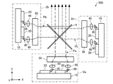
まず、第1実施形態に係る照明装置について図面を参照しながら説明する。図1は、第1実施形態に係る照明装置100の構成を模式的に示す図である。なお、図1および以下に示す図2〜図23、図25、図26には、互いに直交する3つの軸として、X軸、Y軸、およびZ軸を図示している。
1. First Embodiment 1.1. Lighting Device First, the lighting device according to the first embodiment will be described with reference to the drawings. FIG. 1 is a view schematically showing the configuration of the illumination device 100 according to the first embodiment. Note that, in FIG. 1 and FIGS. 2 to 23, 25, and 26 shown below, an X axis, a Y axis, and a Z axis are illustrated as three axes orthogonal to each other.

照明装置100は、図1に示すように、第1照明ユニット2aと、第2照明ユニット2bと、光合成部4と、を含む。   The lighting apparatus 100 includes a first lighting unit 2a, a second lighting unit 2b, and a light combining unit 4, as shown in FIG.

第1照明ユニット2aおよび第2照明ユニット2bは、光源基板(基板の一例)10と、複数の半導体発光素子20と、複数の折り曲げ部30と、複数のコリメート部40と、光学部50と、を含んで構成されている。なお、図1では、便宜上、照明装置100を構成する各部材を簡略化して図示している。   The first lighting unit 2 a and the second lighting unit 2 b are a light source substrate (an example of a substrate) 10, a plurality of semiconductor light emitting devices 20, a plurality of bending portions 30, a plurality of collimating portions 40, and an optical portion 50. Is composed including. In addition, in FIG. 1, each member which comprises the illuminating device 100 is simplified and shown in figure for convenience.

第1照明ユニット2aおよび第2照明ユニット2bでは、図1に示すように、光源基板10の主面(第1面)に実装されている複数の半導体発光素子20が光源基板10の主面の面内方向に光を射出する。複数の半導体発光素子20から射出された光の各々は、折り曲げ部30によって光源基板10の主面から離れる方向に折り曲げられ、コリメート部40によって平行化される。コリメート部40によって平行化された光は光学部50に入射
し、光学部50によって光軸間の距離が短くなり、光束Pa,Pbとして射出される。光束Pa,Pbは共に、複数の光束によって構成されるアレイ光束である。
In the first lighting unit 2 a and the second lighting unit 2 b, as shown in FIG. 1, the plurality of semiconductor light emitting elements 20 mounted on the main surface (first surface) of the light source substrate 10 is the main surface of the light source substrate 10. Emit light in the in-plane direction. Each of the light emitted from the plurality of semiconductor light emitting elements 20 is bent in a direction away from the main surface of the light source substrate 10 by the bending portion 30, and is collimated by the collimating portion 40. The light collimated by the collimating unit 40 enters the optical unit 50, the distance between the optical axes is shortened by the optical unit 50, and the light is emitted as light beams Pa and Pb. The luminous fluxes Pa and Pb are both array luminous fluxes constituted by a plurality of luminous fluxes.

第1照明ユニット2aから射出された第1の光束Paおよび第2照明ユニット2bから射出された第2の光束Pbは、光合成部4によって合成される。照明装置100は、第1の光束Paと第2の光束Pbとが合成された合成光束を射出する。   The first light flux Pa emitted from the first lighting unit 2 a and the second light flux Pb emitted from the second lighting unit 2 b are synthesized by the light synthesis unit 4. The illumination device 100 emits a combined light beam in which the first light beam Pa and the second light beam Pb are combined.

以下、照明装置100を構成する各部材について詳細に説明する。   Hereinafter, each member which comprises the illuminating device 100 is demonstrated in detail.

(1)照明ユニット
まず、第1照明ユニット2aについて説明する。図2は、第1照明ユニット2aを模式的に示す平面図である。図3は、第1照明ユニット2aを模式的に示す図2のIII−III線断面図である。なお、図2および図3では、便宜上、光学部50の図示を省略している。
(1) Lighting Unit First, the first lighting unit 2a will be described. FIG. 2 is a plan view schematically showing the first lighting unit 2a. FIG. 3 is a cross-sectional view taken along line III-III of FIG. 2 schematically showing the first lighting unit 2a. In FIGS. 2 and 3, the optical unit 50 is omitted for the sake of convenience.

光源基板10は、シリコン等の半導体基板である。光源基板10の主面(第1面)11a(+Z軸方向を向く面)には、複数の半導体発光素子20が実装されている。光源基板10の主面11b(主面11aの反対側の主面、−Z軸方向を向く面)には、放熱板12が設けられている。放熱板12の材質は、銅等の熱伝導性に優れた材料であり、放熱板12によって半導体発光素子20の動作時の熱を逃がすことができる。これにより、半導体発光素子20の発光効率の低下を抑制することができる。   The light source substrate 10 is a semiconductor substrate such as silicon. A plurality of semiconductor light emitting elements 20 are mounted on the main surface (first surface) 11 a (surface facing in the + Z axis direction) of the light source substrate 10. The heat sink 12 is provided on the main surface 11 b (the main surface on the opposite side of the main surface 11 a, the surface facing the −Z-axis direction) of the light source substrate 10. The material of the heat sink 12 is a material excellent in thermal conductivity, such as copper, and the heat can be dissipated by the heat sink 12 when the semiconductor light emitting device 20 operates. Thereby, the fall of the luminous efficiency of the semiconductor light-emitting device 20 can be suppressed.

複数の半導体発光素子20は、光源基板10の主面11aに実装されている。複数の半導体発光素子20は、複数行複数列(マトリックス状)に配置されている。すなわち、複数の半導体発光素子20は、2次元アレイ状に配置されている。図示の例では、Y軸方向に並べられた4つの半導体発光素子20からなる列が、X軸方向に2列配置されている。このように、第1照明ユニット2aでは、4行2列に配置された8個の半導体発光素子20をアレイ化して、1つのアレイ光源ユニットを構成している。なお、半導体発光素子20の数は、特に限定されない。   The plurality of semiconductor light emitting devices 20 are mounted on the major surface 11 a of the light source substrate 10. The plurality of semiconductor light emitting devices 20 are arranged in a plurality of rows and columns (in a matrix). That is, the plurality of semiconductor light emitting devices 20 are arranged in a two-dimensional array. In the illustrated example, two rows of four semiconductor light emitting elements 20 arranged in the Y-axis direction are arranged in the X-axis direction. As described above, in the first lighting unit 2a, eight semiconductor light emitting elements 20 arranged in four rows and two columns are arrayed to constitute one array light source unit. The number of semiconductor light emitting elements 20 is not particularly limited.

半導体発光素子20は、光源基板10の主面11aの面内方向に光を射出する。図示の例では、半導体発光素子20は、+X軸方向に光を射出する。   The semiconductor light emitting element 20 emits light in the in-plane direction of the main surface 11 a of the light source substrate 10. In the illustrated example, the semiconductor light emitting element 20 emits light in the + X axis direction.

図4は、半導体発光素子20と、当該半導体発光素子20に対応する折り曲げ部30およびコリメート部40と、を模式的に示す断面図である。以下、半導体発光素子20がInGaAlP系(赤色)の端面発光型半導体レーザーである場合について説明する。   FIG. 4 is a cross-sectional view schematically showing the semiconductor light emitting device 20 and the bending portion 30 and the collimating portion 40 corresponding to the semiconductor light emitting device 20. As shown in FIG. Hereinafter, the case where the semiconductor light emitting device 20 is an InGaAlP-based (red) edge-emitting semiconductor laser will be described.

半導体発光素子20は、図4に示すように、活性層106を含む積層体101と、第1電極110と、第2電極112と、を含んで構成されている。   As shown in FIG. 4, the semiconductor light emitting device 20 is configured to include the stacked body 101 including the active layer 106, the first electrode 110, and the second electrode 112.

積層体101は、ベース層102と、第1クラッド層104と、活性層106と、第2クラッド層108と、を含んで構成されている。積層体101は、ベース層(基板)102上に、第1クラッド層104、活性層106、および第2クラッド層108をこの順でエピタキシャル成長させることで形成される。   The stacked body 101 is configured to include a base layer 102, a first cladding layer 104, an active layer 106, and a second cladding layer 108. The stacked body 101 is formed by epitaxially growing the first cladding layer 104, the active layer 106, and the second cladding layer 108 in this order on the base layer (substrate) 102.

ベース層102は、例えば、基板と、バッファー層と、を含む。基板としては、例えば、第1導電型(例えばn型)のGaAs基板などを用いることができる。バッファー層は、例えば、n型のGaAs層、AlGaAs層、InGaP層等である。バッファー層は、エピタキシャル成長させる際に、その上方に形成される層の結晶性を向上させることができる。   The base layer 102 includes, for example, a substrate and a buffer layer. As the substrate, for example, a GaAs substrate of the first conductivity type (for example, n-type) can be used. The buffer layer is, for example, an n-type GaAs layer, an AlGaAs layer, an InGaP layer or the like. The buffer layer can improve the crystallinity of a layer formed thereabove during epitaxial growth.

第1クラッド層104は、ベース層102上に形成されている。第1クラッド層104は、例えば、n型のInGaAlP層である。   The first cladding layer 104 is formed on the base layer 102. The first cladding layer 104 is, for example, an n-type InGaAlP layer.

活性層106は、第1クラッド層104上に形成されている。活性層106は、第1クラッド層104および第2クラッド層108で挟まれている。活性層106は、例えば、InGaPウェル層とInGaAlPバリア層とから構成される量子井戸構造を3つ重ねた多重量子井戸(MQW)構造を有している。   The active layer 106 is formed on the first cladding layer 104. The active layer 106 is sandwiched between the first cladding layer 104 and the second cladding layer 108. The active layer 106 has, for example, a multiple quantum well (MQW) structure in which three quantum well structures including an InGaP well layer and an InGaAlP barrier layer are stacked.

活性層106は、電流が注入されて光を発生させることが可能な層である。活性層106の一部は、活性層106にて発生した光を導波させる光導波路22を構成している。   The active layer 106 is a layer through which current can be injected to generate light. A part of the active layer 106 constitutes an optical waveguide 22 for guiding the light generated in the active layer 106.

光導波路22は、活性層106の−X軸方向側の側面と、活性層106の+X軸方向側の側面と、を接続している。光導波路22は、Z軸方向(活性層106と第1クラッド層104との積層方向)からみて、活性層106の2つの側面間に直線状に設けられており、活性層106の側面(光射出面を含む側面)の垂線に対して平行に設けられている。活性層106で生じた光は、活性層106の2つの側面間で多重反射し、レーザー発振する。活性層106で生じた光は、活性層106の一方の側面(+X軸方向側の側面)に設けられている光射出面から+X軸方向に射出される。   The optical waveguide 22 connects the side surface on the −X axis direction side of the active layer 106 and the side surface on the + X axis direction side of the active layer 106. The optical waveguide 22 is provided linearly between the two side surfaces of the active layer 106 as viewed in the Z-axis direction (the stacking direction of the active layer 106 and the first cladding layer 104), and the side surfaces of the active layer 106 (light It is provided parallel to the vertical line of the side surface including the exit surface. The light generated in the active layer 106 is multi-reflected between two sides of the active layer 106 and oscillates. The light generated in the active layer 106 is emitted in the + X-axis direction from the light emission surface provided on one side surface (the side surface on the + X-axis direction side) of the active layer 106.

第2クラッド層108は、活性層106上に形成されている。第2クラッド層108は、例えば、第2導電型(例えばp型)のInGaAlP層である。   The second cladding layer 108 is formed on the active layer 106. The second cladding layer 108 is, for example, an InGaAlP layer of a second conductivity type (for example, p-type).

第1電極110は、ベース層102の下に形成されている。第2電極112は、第2クラッド層108上に形成されている。第2電極112と第2クラッド層108との間にはコンタクト層(図示せず)が設けられていてもよい。例えば、第2電極112と、第2電極112とオーミックコンタクトする層と、の接触面の平面形状(Z軸方向から見た形状)によって電極110,112間の電流経路が決定され、その結果、光導波路22の平面形状が決定される。   The first electrode 110 is formed under the base layer 102. The second electrode 112 is formed on the second cladding layer 108. A contact layer (not shown) may be provided between the second electrode 112 and the second cladding layer 108. For example, the current path between the electrodes 110 and 112 is determined by the planar shape (the shape as viewed from the Z-axis direction) of the contact surface of the second electrode 112 and the layer in ohmic contact with the second electrode 112. The planar shape of the light guide 22 is determined.

半導体発光素子20は、活性層に屈折率差を設けて光を閉じ込める、いわゆる屈折率導波型であってもよいし、電流を注入することによって生じた光導波路がそのまま導波領域となる、いわゆる利得導波型であってもよい。   The semiconductor light emitting device 20 may be a so-called refractive index waveguide type in which a refractive index difference is provided in the active layer to confine light, or an optical waveguide generated by injecting a current directly becomes a waveguide region. It may be a so-called gain guide type.

半導体発光素子20は、活性層106の面内方向に沿って進行する光が共振する端面発光型の発光素子であるため、例えば活性層の面内方向と直交する方向に進行する光が共振する面発光型の発光素子と比べて、1つの素子から得られる光の出力を高めることができる。   The semiconductor light emitting element 20 is an edge-emitting light emitting element in which light traveling along the in-plane direction of the active layer 106 resonates. For example, light traveling in a direction orthogonal to the in-plane direction of the active layer resonates The output of light obtained from one element can be increased as compared with a surface-emitting light-emitting element.

また、半導体発光素子20は、端面発光型の発光素子であるため、半導体発光素子20から射出される光は、当該光の光軸と直交する2つの方向で大きく異なる拡がり角を持つ。図示の例では、半導体発光素子20から射出される光(X軸方向に進行する光)は、Y軸方向の拡がり角よりもZ軸方向の拡がり角が大きい。すなわち、半導体発光素子20から射出される光の断面形状は、Z軸に沿った長軸を有する楕円状(または略楕円状)である。   In addition, since the semiconductor light emitting element 20 is an edge emitting type light emitting element, light emitted from the semiconductor light emitting element 20 has greatly different spread angles in two directions orthogonal to the optical axis of the light. In the illustrated example, the light emitted from the semiconductor light emitting element 20 (the light traveling in the X-axis direction) has a larger spread angle in the Z-axis direction than the spread angle in the Y-axis direction. That is, the cross-sectional shape of the light emitted from the semiconductor light emitting element 20 is elliptical (or substantially elliptical) having a major axis along the Z axis.

上記では、InGaAlP系の発光素子について説明したが、半導体発光素子20としては、光導波路が形成可能なあらゆる材料系を用いることができる。例えば、AlGaN系、GaN系、InGaN系、GaAs系、AlGaAs系、InGaAs系、InGaAsP系、InP系、GaP系、AlGaP系、ZnCdSe系などの半導体材料を用い
ることができる。
Although the InGaAlP-based light emitting device has been described above, as the semiconductor light emitting device 20, any material system in which an optical waveguide can be formed can be used. For example, semiconductor materials such as AlGaN-based, GaN-based, InGaN-based, GaAs-based, AlGaAs-based, InGaAs-based, InGaAsP-based, InP-based, InP-based, GaP-based, AlGaP-based, and ZnCdSe-based can be used.

折り曲げ部30は、半導体発光素子20から射出された光を光源基板10の主面11aから離れる方向に折り曲げる。図示の例では、折り曲げ部30は、半導体発光素子20から射出された+X軸方向に進行する光を折り曲げて+Z軸方向に進行する光とする。   The bending portion 30 bends the light emitted from the semiconductor light emitting element 20 in the direction away from the major surface 11 a of the light source substrate 10. In the illustrated example, the bending portion 30 bends the light traveling in the + X-axis direction emitted from the semiconductor light emitting element 20 into light traveling in the + Z-axis direction.

折り曲げ部30は、光学基板45に設けられている。折り曲げ部30は、例えば、図2および図3に示すようにプリズム状であり、半導体発光素子20から射出される光の光軸に垂直な入射面31と、半導体発光素子20から射出される光の光軸に対して45度傾いた反射面32と、を有している。   The bent portion 30 is provided on the optical substrate 45. The bent portion 30 has, for example, a prism shape as shown in FIGS. 2 and 3, and the incident surface 31 perpendicular to the optical axis of the light emitted from the semiconductor light emitting device 20 and the light emitted from the semiconductor light emitting device 20 And a reflecting surface 32 inclined 45 degrees with respect to the optical axis of the lens.

反射面32は、光源基板10の主面11aに対して45度傾いている。反射面32には、反射膜(図示せず)が設けられている。半導体発光素子20から射出された光は反射面32にて反射されて、光源基板10の主面11aから離れる方向に折り曲げられる。折り曲げ部30は、複数の半導体発光素子20に1対1に対応して複数設けられている。なお、半導体発光素子20から射出される光の光軸に対して入射面31を垂直に設置する必要はない。また、反射面32の光の光軸に対する傾きは45度に限定されず、主面11aの面内方向に進行する光を主面11aから離れる方向(+Z軸方向側)に折り曲げることができる傾きであればよい。   The reflective surface 32 is inclined 45 degrees with respect to the major surface 11 a of the light source substrate 10. A reflective film (not shown) is provided on the reflective surface 32. The light emitted from the semiconductor light emitting element 20 is reflected by the reflecting surface 32 and is bent in the direction away from the major surface 11 a of the light source substrate 10. A plurality of bent portions 30 are provided in one-to-one correspondence with the plurality of semiconductor light emitting elements 20. It is not necessary to set the incident surface 31 perpendicular to the optical axis of the light emitted from the semiconductor light emitting element 20. Further, the inclination of the light of the reflection surface 32 with respect to the optical axis is not limited to 45 degrees, and an inclination capable of bending light traveling in the in-plane direction of the main surface 11a in a direction away from the main surface 11a (+ Z axis direction side) If it is

コリメート部40は、折り曲げ部30によって折り曲げられた光を平行化する。コリメート部40は、光学基板45に設けられている。コリメート部40は、図示の例では、レンズ(コリメートレンズ)で構成されている。コリメート部40では、折り曲げ部30から射出された光を平行化して、平行光(または略平行光)として射出する。また、コリメート部40は、例えば、光を平行化するとともに、光軸に直交する断面形状を円形状または楕円形状にする。コリメート部40は、複数の折り曲げ部30に1対1に対応して複数設けられている。   The collimating unit 40 collimates the light bent by the bending unit 30. The collimating unit 40 is provided on the optical substrate 45. The collimating unit 40 is configured of a lens (collimating lens) in the illustrated example. The collimating unit 40 collimates the light emitted from the bending unit 30 and emits the light as parallel light (or substantially parallel light). Further, for example, the collimating unit 40 collimates the light and makes the cross-sectional shape orthogonal to the optical axis a circular shape or an elliptical shape. A plurality of collimator parts 40 are provided in one-to-one correspondence with the plurality of bending parts 30.

第1照明ユニット2aでは、折り曲げ部30と、コリメート部40を構成している光学素子(レンズ)と、が一体に構成されている。図示の例では、第1照明ユニット2aは、折り曲げ部30と、コリメート部40と、が一体に形成された光学基板45を有している。   In the first illumination unit 2a, the bending portion 30 and the optical element (lens) constituting the collimating portion 40 are integrally configured. In the illustrated example, the first lighting unit 2a has an optical substrate 45 in which the bending portion 30 and the collimating portion 40 are integrally formed.

光学基板45は、ガラスや石英等の無機材料、プラスチック等の樹脂材料からなる透明基板を母材にして形成されている。光学基板45は、支持部47を有しており、支持部47は光源基板10の主面11aと接着剤等により接合されている。光学基板45の、光源基板10の主面11aと対向する面側(−Z軸方向側)には、凹部46が設けられている。光源基板10と光学基板45とが接続された状態で、凹部46内に半導体発光素子20が収容される。すなわち、半導体発光素子20は、光源基板10と光学基板45とに囲まれた空間内に収容されている。   The optical substrate 45 is formed using a transparent substrate made of an inorganic material such as glass or quartz, or a resin material such as plastic as a base material. The optical substrate 45 has a support portion 47, and the support portion 47 is bonded to the main surface 11a of the light source substrate 10 by an adhesive or the like. A recess 46 is provided on the surface of the optical substrate 45 facing the main surface 11 a of the light source substrate 10 (−Z-axis direction side). The semiconductor light emitting element 20 is accommodated in the recess 46 in a state where the light source substrate 10 and the optical substrate 45 are connected. That is, the semiconductor light emitting element 20 is accommodated in a space surrounded by the light source substrate 10 and the optical substrate 45.

光学基板45では、凹部46の底面を規定する面(−Z軸方向側の面)から半導体発光素子20側(−Z軸方向側)に張り出したプリズム形状の部分が、折り曲げ部30を構成している。図2に示すように、Y軸に沿って配列されている複数(4個)の半導体発光素子20に対応する複数(4個)の折り曲げ部30は連続している。   In the optical substrate 45, a prism-shaped portion protruding from the surface defining the bottom surface of the recess 46 (the surface on the −Z-axis direction side) toward the semiconductor light emitting element 20 (−Z-axis direction) constitutes the bent portion 30. ing. As shown in FIG. 2, a plurality of (four) bent portions 30 corresponding to a plurality of (four) semiconductor light emitting elements 20 arranged along the Y-axis are continuous.

光学基板45の、凹部46の底面を規定する面とは反対側の面(+Z軸方向側の面)には、コリメート部40を構成しているレンズ面41が設けられている。レンズ面41は、1つの半導体発光素子20に対して、1つ設けられている。レンズ面41は、複数行複数列(アレイ状)に配置された半導体発光素子20に対応して、複数行複数列(アレイ状)
に配置されている。なお、ここでは、光学基板45のレンズ面41がコリメート部40を構成している例について説明したが、光学基板45のレンズ面41を集光レンズとし、コリメート部40を構成する光学素子を光学基板45とは別部材として設けてもよい。
A lens surface 41 constituting a collimating portion 40 is provided on the surface of the optical substrate 45 opposite to the surface defining the bottom surface of the recess 46 (the surface on the + Z-axis direction side). One lens surface 41 is provided for one semiconductor light emitting element 20. The lens surface 41 corresponds to a plurality of rows and a plurality of columns (array) corresponding to the semiconductor light emitting elements 20 arranged in a plurality of rows and a plurality of columns (array).
Is located in Here, although the example in which the lens surface 41 of the optical substrate 45 constitutes the collimator unit 40 has been described, the lens surface 41 of the optical substrate 45 is a condensing lens, and the optical element constituting the collimator unit 40 is optical The substrate 45 may be provided as a separate member.

光源基板10、複数の半導体発光素子20、および光学基板45の各々には、位置合わせ用のマーク(図示せず)が形成されており、これらの位置合わせ用のマークを用いて、複数の半導体発光素子20と光学基板45との相対的な位置を合わせることができる。これにより、半導体発光素子20から射出された光を、折り曲げ部30およびコリメート部40の所定の位置に正確に入射させることができる。   Alignment marks (not shown) are formed on each of the light source substrate 10, the plurality of semiconductor light emitting elements 20, and the optical substrate 45, and a plurality of semiconductors are formed using these alignment marks. The relative positions of the light emitting element 20 and the optical substrate 45 can be matched. Thus, the light emitted from the semiconductor light emitting element 20 can be accurately incident on the predetermined position of the bending portion 30 and the collimating portion 40.

半導体発光素子20から射出された光は、折り曲げ部30の入射面31から入射し、反射面32で反射されて、光源基板10の主面11aから離れる方向に折り曲げられる。そして、反射面32で反射された光は、コリメート部40(レンズ面41)で平行化されて射出される。このようにしてコリメート部40から射出された光Lは、平行光(または略平行光)になるとともに、光軸に直交する断面形状が円形状または楕円形状になる。   The light emitted from the semiconductor light emitting element 20 is incident from the incident surface 31 of the bent portion 30, is reflected by the reflecting surface 32, and is bent in the direction away from the major surface 11 a of the light source substrate 10. Then, the light reflected by the reflection surface 32 is collimated by the collimator unit 40 (lens surface 41) and emitted. Thus, the light L emitted from the collimating unit 40 becomes parallel light (or substantially parallel light), and the cross-sectional shape orthogonal to the optical axis becomes circular or elliptical.

図5(A)は、複数のコリメート部40から射出された光束P1を模式的に示す図である。なお、図5(A)および後述する図5(B)は、光源光軸Aと直交する断面を図示している。ここで、光源光軸Aとは、第1の光束Paの光軸である。光源光軸Aは、光束P1の光軸と一致している。   FIG. 5A is a view schematically showing the light flux P1 emitted from the plurality of collimator sections 40. As shown in FIG. FIG. 5A and FIG. 5B to be described later illustrate a cross section orthogonal to the light source optical axis A. Here, the light source optical axis A is the optical axis of the first light flux Pa. The light source optical axis A coincides with the optical axis of the light flux P1.

図5(A)に示すように、各コリメート部40から射出された光Lで構成された光束P1は、光源光軸Aに直交する平面内において、光Lが複数行複数列(アレイ状)に配置されている。すなわち、光束P1は、複数行複数列に配置された光Lで構成されている。図示の例では、光束P1は、4行2列に配置された半導体発光素子20の配置に対応して、4行2列に配置された光Lで構成されている。なお、複数の半導体発光素子20の各々の仕様を揃えることで、光Lの径や強度がそろった光束P1を得ることができる。   As shown in FIG. 5A, in the plane orthogonal to the light source optical axis A, the light flux P1 composed of the light L emitted from each of the collimator sections 40 has a plurality of rows and a plurality of columns (array shape) Is located in That is, the light flux P1 is composed of the light L arranged in a plurality of rows and a plurality of columns. In the illustrated example, the light flux P1 is made up of light L arranged in four rows and two columns, corresponding to the arrangement of the semiconductor light emitting elements 20 arranged in four rows and two columns. Note that by aligning the specifications of each of the plurality of semiconductor light emitting elements 20, it is possible to obtain a light flux P1 in which the diameter and the intensity of the light L are uniform.

光学部50は、複数のコリメート部40で平行化された光Lの光軸間の距離を短くする。図6(A)は、光学部50を模式的に示す平面図(Z軸方向から見た図)である。図6(B)は、光学部50をY軸方向から見た模式図であり、図6(C)は、光学部50をX軸方向から見た模式図である。   The optical unit 50 shortens the distance between the optical axes of the light L collimated by the plurality of collimating units 40. FIG. 6A is a plan view schematically showing the optical unit 50 (a view from the Z-axis direction). 6B is a schematic view of the optical unit 50 viewed from the Y-axis direction, and FIG. 6C is a schematic view of the optical unit 50 viewed from the X-axis direction.

光学部50は、透光性材料からなる光学素子であり、図示の例ではプリズムアレイによって構成されている。光学部50は、光Lが入射する一方側(−Z軸方向側)に形成された複数の入射端面52と、光Lが射出する他方側(+Z軸方向側)に形成された複数の射出端面54と、を有している。   The optical unit 50 is an optical element made of a translucent material, and in the illustrated example, is configured by a prism array. The optical unit 50 has a plurality of incident end faces 52 formed on one side (−Z-axis direction side) on which the light L is incident, and a plurality of ejections formed on the other side (+ Z-axis direction side) on which the light L is emitted. And an end face 54.

光学部50では、一対の入射端面52と射出端面54の素子上の位置における傾斜の度合い(傾斜角度)、入射端面52と射出端面54との間の距離、透光性材料の屈折率等を制御因子として、複数のコリメート部40から射出される光の各々の位置を調整して射出することができる。   In the optical unit 50, the degree of inclination (tilt angle) at the position on the element of the pair of incident end face 52 and the exit end face 54, the distance between the incident end face 52 and the exit end face 54, the refractive index of the translucent material, etc. As a control factor, the position of each of the light emitted from the plurality of collimating units 40 can be adjusted and emitted.

図示の例では、入射端面52は、位置に応じて所定の傾斜角(入射する光の光軸に対する角度)で形成されている。具体的には、入射端面52は、例えば光源光軸Aとの距離が大きい入射端面ほど傾斜角が大きくなる。   In the illustrated example, the incident end face 52 is formed at a predetermined inclination angle (an angle with respect to the optical axis of incident light) depending on the position. Specifically, the inclination angle of the incident end surface 52 is larger as the distance to the light source optical axis A is larger, for example.

射出端面54は、対応する入射端面52と同じ傾斜角を有している。すなわち、対応関係にある入射端面52と射出端面54とは平行である。射出端面54と光源光軸Aとの間の距離は、対応する入射端面52と光源光軸Aとの間の距離よりも短い。   The injection end face 54 has the same inclination angle as the corresponding entrance end face 52. That is, the incident end face 52 and the exit end face 54 in a corresponding relationship are parallel to each other. The distance between the emitting end surface 54 and the light source optical axis A is shorter than the distance between the corresponding incident end surface 52 and the light source optical axis A.

光学部50では、ある入射端面52(例えば入射端面52a)に入射した光は、対応する射出端面54(例えば射出端面54a)から射出される。ここで、対応関係にある一対の入射端面52と射出端面54とは平行であるため、光学部50に入射した光は、角度分布を維持しながら、位置のみを変化させる。すなわち、光学部50は、入射した光を平行シフトさせる。また、上述したように、射出端面54と光源光軸Aとの間の距離は、対応する入射端面52と光源光軸Aとの間の距離よりも短いため、ある射出端面54(例えば射出端面54a)から射出された光の光軸と光源光軸Aとの間の距離を、対応する入射端面52(例えば入射端面52a)に入射した光の光軸と光源光軸Aとの間の距離よりも短くすることができる。すなわち、光学部50は、入射した光の光軸の位置を光源光軸A側に平行シフトさせることができる。   In the optical unit 50, light incident on an incident end surface 52 (for example, the incident end surface 52a) is emitted from the corresponding emission end surface 54 (for example, the emission end surface 54a). Here, since the pair of incident end faces 52 and the exit end face 54 in a corresponding relationship are parallel to each other, the light incident on the optical unit 50 changes only the position while maintaining the angular distribution. That is, the optical unit 50 shifts the incident light in parallel. Further, as described above, since the distance between the emission end surface 54 and the light source optical axis A is shorter than the distance between the corresponding incident end surface 52 and the light source optical axis A, a certain emission end surface 54 (for example, the emission end surface The distance between the optical axis of the light emitted from 54a) and the light source optical axis A is the distance between the optical axis of the light incident on the corresponding incident end face 52 (for example, the incident end face 52a) and the light source optical axis A It can be shorter than That is, the optical unit 50 can shift the position of the optical axis of the incident light parallel to the light source optical axis A side.

例えば、光源光軸Aに対して+Y軸方向側であって、かつ、+X軸方向側に位置している入射端面52aに入射した光は、図6(B)に示すように、XZ平面内において、入射端面52aで−X軸方向に屈折して対応する射出端面54aに至り、射出端面54aで+X軸方向に屈折して射出される。また、入射端面52aに入射した光は、図6(C)に示すように、YZ平面内において、入射端面52aで−Y軸方向に屈折して対応する射出端面54aに至り、射出端面54aで+Y軸方向に屈折して射出される。このとき、入射端面52aと射出端面54aとは平行であるため、光学部50に入射した光は、平行性を維持しながら、光の光軸の位置を光源光軸A側に平行シフトする。   For example, as shown in FIG. 6B, light incident on the incident end face 52a located on the + Y axis direction side and on the + X axis direction side with respect to the light source optical axis A is in the XZ plane. The light is refracted in the −X-axis direction at the incident end face 52a to reach the corresponding exit end face 54a, and refracted and emitted in the + X-axis direction at the exit end face 54a. Further, as shown in FIG. 6C, the light incident on the incident end surface 52a is refracted in the −Y axis direction at the incident end surface 52a in the YZ plane to reach the corresponding emission end surface 54a, and is output on the emission end surface 54a The light is refracted and emitted in the + Y axis direction. At this time, since the incident end face 52a and the emission end face 54a are parallel to each other, the light incident on the optical unit 50 shifts the position of the optical axis of the light parallel to the light source optical axis A while maintaining parallelism.

第1照明ユニット2aでは、複数のコリメート部40から射出された、互いに平行な光Lの各々が光学部50の各入射端面52に入射し、光学部50にて平行シフトされて射出される。すなわち、光学部50の各射出端面54から射出された光Lの各々は、互いに平行である。そのため、2次元アレイ状の光は光学部50を経ることによって、各々の光の平行性を保ちつつ、隣接する光の間隔を狭くすることができる。すなわち、エテンデューを小さくして、後段の光学系において光の利用効率を高めることができる。   In the first illumination unit 2a, the parallel lights L emitted from the plurality of collimating units 40 are incident on the respective incident end faces 52 of the optical unit 50, are parallel-shifted by the optical unit 50, and are emitted. That is, the respective lights L emitted from the respective emission end faces 54 of the optical unit 50 are parallel to one another. Therefore, by passing the two-dimensional array light through the optical unit 50, the distance between the adjacent lights can be narrowed while maintaining the parallelism of each light. That is, the etendue can be reduced to improve the utilization efficiency of light in the subsequent optical system.

図5(B)は、第1の光束Pa(光学部50から射出された光)を模式的に示す図である。なお、図5(B)では、光学部50に入射する光束P1を構成する光Lを波線の円で示し、光学部50から射出された第1の光束Paを構成する光Lを実線の円で示している。   FIG. 5B is a view schematically showing the first light flux Pa (light emitted from the optical unit 50). In FIG. 5B, the light L constituting the light flux P1 incident on the optical unit 50 is indicated by a broken line circle, and the light L constituting the first light flux Pa emitted from the optical unit 50 is indicated by a solid circle It shows by.

図5(B)に示すように、第1の光束Paは、光源光軸Aに直交する平面内において、複数行複数列(図示の例では4行2列)に配置された光Lで構成されている。すなわち、第1の光束Paは、2次元アレイ状に配置された光Lで構成されている。図示の例では、第1の光束Paでは、光源光軸Aと直交する平面内において、光LがX軸方向に光径Wの2倍のピッチで配置され、Y軸方向に光径Wと同じピッチで配置されている。隣り合う第1の光束Paを構成する光Lの列間の距離は、光径Wと同じ(または略同じ)である。なお、光径Wは、例えば、光Lの光強度がピーク強度値の約13.5%(1/e)となるところの幅(直径)とする。 As shown in FIG. 5B, the first light flux Pa is composed of light L arranged in a plurality of rows and a plurality of columns (4 rows and 2 columns in the illustrated example) in a plane orthogonal to the light source optical axis A. It is done. That is, the first light flux Pa is composed of the light L arranged in a two-dimensional array. In the illustrated example, in the first light flux Pa, the light L is disposed in the X axis direction at a pitch twice the light diameter W in a plane orthogonal to the light source optical axis A, and the light diameter W in the Y axis direction It is arranged at the same pitch. The distance between the rows of light L constituting the adjacent first light flux Pa is the same (or substantially the same) as the light diameter W. The light diameter W is, for example, the width (diameter) at which the light intensity of the light L is about 13.5% (1 / e 2 ) of the peak intensity value.

第1の光束Paは、上述したように光学部50によって、光束P1を構成する光Lの光軸を光源光軸A側に平行シフトさせて光Lの光軸間の距離を短くすることにより得られる。図示の例では、光束P1では、光源光軸Aと直交する断面において、光LがX軸方向には光径(光Lの直径)Wの4倍のピッチで配置され、Y軸方向には光径Wの1.5倍のピッチで配置されている。光学部50では、光束P1を構成する光Lの光軸間の距離を、X軸方向に光径Wの2倍分だけ短くし、Y軸方向に光径Wの0.5倍分だけ短くする。これにより、第1の光束Paが得られる。   As described above, the first luminous flux Pa is parallel-shifted toward the light source optical axis A by the optical unit 50 so as to shorten the distance between the optical axes of the light L. can get. In the illustrated example, in the light flux P1, the light L is disposed at a pitch four times the light diameter (diameter of the light L) W in the X-axis direction in the cross section orthogonal to the light source optical axis A It is disposed at a pitch of 1.5 times the light diameter W. In the optical unit 50, the distance between the optical axes of the light L constituting the light flux P1 is shortened by twice the light diameter W in the X-axis direction, and shortened by 0.5 times the light diameter W in the Y-axis direction. Do. Thereby, the first luminous flux Pa is obtained.

次に、第2照明ユニット2bについて説明する。第2照明ユニット2bの構成は、上述した第1照明ユニット2aと同様であり、その詳細な説明を省略する。   Next, the second lighting unit 2b will be described. The configuration of the second lighting unit 2b is the same as that of the first lighting unit 2a described above, and the detailed description thereof will be omitted.

第2照明ユニット2bは、第2照明ユニット2bから射出される第2の光束Pbの光軸が、第1照明ユニット2aから射出される第1の光束Paの光軸と交差するように配置される。図示の例では、第1照明ユニット2aが光源基板10の主面11a(図3参照)が+Z軸方向を向くように配置され、第1の光束Paを+Z軸方向に射出するのに対して、第2照明ユニット2bは、光源基板10の主面11aが+X軸方向を向くように配置され、第2の光束Pbを+X軸方向に射出する。   The second illumination unit 2b is disposed such that the optical axis of the second luminous flux Pb emitted from the second illumination unit 2b intersects the optical axis of the first luminous flux Pa emitted from the first illumination unit 2a. Ru. In the illustrated example, the first illumination unit 2a is disposed so that the main surface 11a (see FIG. 3) of the light source substrate 10 faces the + Z axis direction, and emits the first light flux Pa in the + Z axis direction. The second illumination unit 2b is disposed such that the major surface 11a of the light source substrate 10 faces the + X axis direction, and emits the second light beam Pb in the + X axis direction.

(2)光合成部
次に、光合成部4について説明する。
(2) Light Combining Unit Next, the light combining unit 4 will be described.

光合成部4は、第1照明ユニット2aから射出される第1の光束Paと、第2照明ユニット2bから射出される第2の光束Pbと、を合成する。光合成部4は、第1の光束Paを構成する光Lの列と、第2の光束Pbを構成する光Lの列と、を交互に配置して、第1の光束Paと第2の光束Pbとを合成する。第1の光束Paおよび第2の光束Pbは、光合成部4にて空間的に光束が合成され、合成光束(合成照明光束)として射出される。   The light combining unit 4 combines the first light flux Pa emitted from the first lighting unit 2a and the second light flux Pb emitted from the second lighting unit 2b. The light combining unit 4 alternately arranges a line of the light L that constitutes the first light flux Pa and a line of the light L that constitutes the second light flux Pb, and thereby the first light flux Pa and the second light flux Synthesize with Pb. The first light flux Pa and the second light flux Pb are spatially combined by the light combining unit 4 and the combined light flux (a combined illumination light flux) is emitted.

図7(A)は、光合成部4を模式的に示す斜視図である。図7(B)は、光合成部4を構成している第1プリズム4aを模式的に示す斜視図であり、図7(C)は、光合成部4を構成している第2プリズム4bを模式的に示す斜視図である。なお、以下の説明では、第1の光束Pa及び第2の光束Pbを構成する各光Lの光径Wは等しいと仮定する。   FIG. 7A is a perspective view schematically showing the light combining unit 4. FIG. 7 (B) is a perspective view schematically showing the first prism 4a constituting the light combining unit 4, and FIG. 7 (C) schematically shows the second prism 4b constituting the light combining unit 4. It is a perspective view shown. In the following description, it is assumed that the light diameters W of the respective lights L constituting the first light flux Pa and the second light flux Pb are equal.

光合成部4は、図7(A)に示すように、透光性材料からなる2つのプリズム4a,4bを斜面が相対(対向)するように接着した光学素子である。プリズム4a,4bは、例えば、直角二等辺三角形を底面とする三角柱状の直角プリズムである。第1プリズム4aの斜面(第2面)402aと、第2プリズム4bの斜面(第3面)402bとの間(界面)には、第1の光束Paを構成する光Lの列を通過させる光通過部410と、第2の光束Pbを構成する光Lの列を反射させる光反射部420と、が設けられている。光通過部410および光反射部420は、複数設けられている。光通過部410と光反射部420とは、プリズム4a,4bの界面の面内方向に、交互に設けられている。図示の例では、光通過部410と光反射部420とは、α軸(Y軸に直交し、かつ、X軸およびZ軸に対して45度傾いた軸)方向に交互に設けられている。   As shown in FIG. 7A, the light combining portion 4 is an optical element in which two prisms 4a and 4b made of a light transmitting material are bonded so that the slopes face each other. The prisms 4a and 4b are, for example, triangular prism-shaped right-angled prisms whose bottom surfaces are right-angled isosceles triangles. A line of light L forming the first light flux Pa is allowed to pass between (the interface) between the slope (second surface) 402 a of the first prism 4 a and the slope (third surface) 402 b of the second prism 4 b. A light passing portion 410 and a light reflecting portion 420 for reflecting a row of light L constituting the second light flux Pb are provided. A plurality of light passing portions 410 and light reflecting portions 420 are provided. The light passing portions 410 and the light reflecting portions 420 are alternately provided in the in-plane direction of the interface between the prisms 4a and 4b. In the illustrated example, the light passing portions 410 and the light reflecting portions 420 are alternately provided in the direction of the α axis (axis orthogonal to the Y axis and inclined 45 degrees with respect to the X axis and the Z axis) .

第1プリズム4aは、図7(B)に示すように、斜面(二等辺三角形の底辺と接続している側面)402aと、2つの側面404a,406aと、を有している。第1プリズム4aの斜面402aには、複数の光反射部420が設けられている。光反射部420としては、半導体発光素子20から射出される光を効率よく反射させる誘電体多層膜等の反射膜が好適である。   As shown in FIG. 7B, the first prism 4a has a slope (a side surface connected to the base of the isosceles triangle) 402a and two side surfaces 404a and 406a. A plurality of light reflecting portions 420 are provided on the slope 402 a of the first prism 4 a. As the light reflecting portion 420, a reflecting film such as a dielectric multilayer film which reflects light emitted from the semiconductor light emitting element 20 efficiently is preferable.

光反射部420の幅(α軸方向の大きさ)Wは、光径Wと同じ(または光径W以上)である。光反射部420の長さ(Y軸方向の長さ)は、第2の光束Pbを構成する光Lの列の長さ(第2の光束PbのY軸方向の長さ)以上である。光反射部420は、第2の光束Pbを構成する光Lの列のピッチと同じピッチで配置されている。図示の例では、光反射部420は、光径Wの2倍のピッチで配置されている。すなわち、光反射部420間の距離は、光径Wと同じ(または光径W以上)である。第1プリズム4aの斜面402aにおいて光反射部420が存在しない領域は、光通過部410となる。すなわち、光通過部410の幅(α軸方向の大きさ)Wは、光径Wと同じ(または光径W以上)である。すなわち、第1プリズム4aの斜面402aには、互いに同じ幅の光通過部410と光反射
部420とが交互に配置されている。なお、上記では光通過部410の幅Wと光反射部420の幅Wを等しく設定する場合を説明したが、これに限定されない。すなわち、後述するように、光合成部4から射出される合成光束Pa+bを構成する光Lが互いに重ならないように密接した状態で配置される様に、第1の光束Pa及び第2の光束Pbを構成する各光Lの光径Wに対応させて、光通過部410及び光反射部420の幅とそれらの配置間隔とを設定することが望ましい。
The width (size in the α-axis direction) W R of the light reflecting portion 420 is the same as the light diameter W (or more than the light diameter W). The length (length in the Y-axis direction) of the light reflecting portion 420 is equal to or longer than the length of the line of light L constituting the second light flux Pb (the length in the Y-axis direction of the second light flux Pb). The light reflecting portions 420 are arranged at the same pitch as the pitch of the rows of the light L constituting the second light flux Pb. In the illustrated example, the light reflecting portions 420 are arranged at a pitch twice the light diameter W. That is, the distance between the light reflecting portions 420 is the same as the light diameter W (or more than the light diameter W). An area where the light reflecting portion 420 does not exist in the slope 402 a of the first prism 4 a is the light passing portion 410. That, W T (the size of the α-axis direction) width of the light passing portion 410 is the same as the optical diameter W (or more optical diameter W). That is, the light passing portions 410 and the light reflecting portions 420 having the same width are alternately arranged on the slope 402 a of the first prism 4 a. In the above description the case of setting equal width W R of width W T and the light reflecting portion 420 of the light passing portion 410 is not limited to this. That is, as described later, the first light flux Pa and the second light flux Pb are arranged so that the light beams L constituting the combined light flux Pa + b emitted from the light combining unit 4 are in close contact with each other so as not to overlap each other. It is desirable to set the widths of the light passing portions 410 and the light reflecting portions 420 and the arrangement intervals thereof in correspondence with the light diameter W of each of the light L to be configured.

第1プリズム4aの側面404aは、第1の光束Paが入射する入射面となる。第1プリズム4aの斜面402aや側面404aには、反射防止膜が形成されていていることが好ましい。   The side surface 404 a of the first prism 4 a is an incident surface on which the first light beam Pa is incident. It is preferable that an antireflective film is formed on the inclined surface 402a and the side surface 404a of the first prism 4a.

第2プリズム4bは、図7(C)に示すように、斜面402bと、2つの側面404b、406bと、を有している。第2プリズム4bは、例えば、第1プリズム4aと同じ形状、同じ大きさを有している。第2プリズム4bの側面406bは、第2の光束Pbが入射する入射面となる。また、第2プリズム4bの側面404bは、光通過部410を通過した第1の光束Paおよび光反射部420で反射された第2の光束Pb(すなわち光合成部4で合成された光束)が射出される射出面となる。第2プリズム4bの斜面402bや側面404b,406bには、反射防止膜が形成されていていることが好ましい。   As shown in FIG. 7C, the second prism 4b has a slope 402b and two side surfaces 404b and 406b. The second prism 4 b has, for example, the same shape and the same size as the first prism 4 a. The side surface 406b of the second prism 4b is an incident surface on which the second light beam Pb is incident. Further, the side surface 404 b of the second prism 4 b emits the first light flux Pa that has passed through the light passing section 410 and the second light flux Pb reflected by the light reflecting section 420 (that is, the light flux synthesized by the light combining section 4). It becomes an injection surface to be It is preferable that an anti-reflection film is formed on the inclined surface 402b and the side surfaces 404b and 406b of the second prism 4b.

なお、ここでは、第1プリズム4aの斜面402aに光反射部420となる反射膜が設けられている例について説明したが、第2プリズム4bの斜面402bに光反射部420となる反射膜が設けられていてもよい。   Here, although the example in which the reflecting film to be the light reflecting portion 420 is provided on the inclined surface 402a of the first prism 4a has been described, the reflecting film to be the light reflecting portion 420 is provided on the inclined surface 402b of the second prism 4b. It may be done.

光合成部4は、第1照明ユニット2aから射出された第1の光束Paと、第2照明ユニット2bから射出された第2の光束Pbとが、交わる位置(または略交わる位置)に配置されている。より具体的には、光合成部4は、第1プリズム4aと第2プリズム4bとの界面が第1の光束Paと第2の光束Pbとが交わる位置(または略交わる位置)に位置するように配置されている。また、第1プリズム4aと第2プリズム4bとの界面は、光束Pa,Pbの光軸に対して45度の角度をなすように配置される。   The light combining unit 4 is disposed at a position where the first light flux Pa emitted from the first lighting unit 2a and the second light flux Pb emitted from the second lighting unit 2b intersect (or substantially intersect) There is. More specifically, the light combining unit 4 is positioned such that the interface between the first prism 4a and the second prism 4b is at a position where the first light flux Pa and the second light flux Pb intersect (or a position where they substantially intersect). It is arranged. Further, the interface between the first prism 4a and the second prism 4b is disposed at an angle of 45 degrees with respect to the optical axes of the light beams Pa and Pb.

図7(A)に示すように、第1照明ユニット2aから射出された第1の光束Paは+Z軸方向に向かって進行し、第1プリズム4aの側面404aに入射する。そして、第1の光束Paは、第1の光束Paを構成する光Lの列ごとに光通過部410を通過して、第2プリズム4bの側面404bから+Z軸方向に射出される。   As shown in FIG. 7A, the first light beam Pa emitted from the first illumination unit 2a travels in the + Z-axis direction and enters the side surface 404a of the first prism 4a. Then, the first light flux Pa passes through the light passing portion 410 for each row of the light L constituting the first light flux Pa, and is emitted from the side surface 404b of the second prism 4b in the + Z-axis direction.

一方、第2照明ユニット2bから射出された第2の光束Pbは+X軸方向に向かって進行し、第2プリズム4bの側面406bに入射する。そして、第2の光束Pbは、第2の光束Pbを構成する光Lの列ごとに光反射部420で反射されて+Z軸方向に進行方向を変えて、第2プリズム4bの側面404bから+Z軸方向に射出される。すなわち、複数の光反射部420は、第2の光束Pbを第1の光束Paの進行方向と同じ方向に向けて反射させる。   On the other hand, the second light beam Pb emitted from the second illumination unit 2b travels in the + X axis direction, and is incident on the side surface 406b of the second prism 4b. Then, the second light flux Pb is reflected by the light reflecting portion 420 for each row of the light L constituting the second light flux Pb and changes its traveling direction in the + Z axis direction, so that + Z from the side surface 404b of the second prism 4b. Ejected in the axial direction. That is, the plurality of light reflecting portions 420 reflect the second light flux Pb in the same direction as the traveling direction of the first light flux Pa.

このように光合成部4は、複数の光反射部420によって第2の光束Pbを第1の光束Paの進行方向と同じ方向に向けて反射させて、第1の光束Paと第2の光束Pbとを合成する。   As described above, the light combining unit 4 causes the plurality of light reflecting units 420 to reflect the second light flux Pb in the same direction as the traveling direction of the first light flux Pa, and thereby the first light flux Pa and the second light flux Pb. And

図8は、光合成部4で合成された合成光束Pa+bを模式的に示す図である。なお、図8は、合成光束Pa+bの、合成光束Pa+bの光軸Oと直交する断面を図示している。   FIG. 8 is a view schematically showing the combined light beam Pa + b combined by the light combining unit 4. FIG. 8 illustrates a cross section of the combined light beam Pa + b orthogonal to the optical axis O of the combined light beam Pa + b.

図8に示すように、合成光束Pa+bは、光軸Oと直交する平面内において、複数行複
数列(図示の例では4行4列)に配置された光Lで構成されている。すなわち、合成光束Pa+bは、2次元アレイ状に配置された光Lで構成されている。合成光束Pa+bは、第1の光束Paを構成する光Lの列と、第2の光束Pbを構成する光Lの列と、がX軸方向に交互に配置されて構成されている。すなわち、隣り合う第1の光束Paを構成する光Lの列間に、第2の光束Pbを構成する光Lの列が位置している。図8に示すように第1の光束Paの光軸Aと第2の光束Pbの光軸Bとを光Lの列と直交する方向(図示の例ではX軸方向)にずらすことで第1の光束Paの光Lの列と第2の光束Pbの光Lの列とを交互に配置することができる。隣り合う第1の光束Pa間の距離(ピッチ)は光径Wの2倍であり、隣り合う第1の光束Pa間の最短距離は光径Wと同じであるため、合成光束Pa+bを構成する光Lは、互いに重ならないように密接した状態で配置される。このように、光合成部4では、第1の光束Paおよび第2の光束Pbを合成して、光束Pa,Pbを構成する光Lの各々が互いに重畳することなく隙間無く隣接するような合成光束Pa+bを得ることができる。
As shown in FIG. 8, in the plane orthogonal to the optical axis O, the combined luminous flux Pa + b is composed of light L arranged in a plurality of rows and a plurality of columns (four rows and four columns in the illustrated example). That is, the combined luminous flux Pa + b is composed of the light L arranged in a two-dimensional array. The combined luminous flux Pa + b is configured by alternately arranging a line of light L constituting the first luminous flux Pa and a line of light L constituting the second luminous flux Pb in the X-axis direction. That is, the row of light L constituting the second light flux Pb is located between the rows of light L constituting the first light flux Pa adjacent to each other. As shown in FIG. 8, by shifting the optical axis A of the first luminous flux Pa and the optical axis B of the second luminous flux Pb in a direction (X-axis direction in the illustrated example) orthogonal to the row of the light L, the first The row of light L of the light flux Pa and the row of light L of the second light flux Pb can be alternately arranged. Since the distance (pitch) between adjacent first light beams Pa is twice the light diameter W, and the shortest distance between adjacent first light beams Pa is the same as the light diameter W, the combined light beam Pa + b is formed. The lights L are arranged in close proximity so as not to overlap each other. As described above, the light combining unit 4 combines the first light flux Pa and the second light flux Pb so that each of the light beams L constituting the light fluxes Pa and Pb is adjacent to each other without a gap without overlapping each other. Pa + b can be obtained.

照明装置100は、例えば、以下の特徴を有する。   The lighting device 100 has, for example, the following features.

照明装置100では、第1照明ユニット2aおよび第2照明ユニット2bにおいて、光源基板10の面内方向に光を射出する複数の半導体発光素子20から射出された光の各々を、折り曲げ部30によって光源基板10の主面11aから離れる方向に折り曲げることができる。すなわち、照明装置100では、端面発光型の半導体発光素子20を用いることができる。したがって、照明装置100では、例えば面発光型の半導体発光素子を用いる場合と比べて、1つの半導体発光素子から得られる光出力を大きくすることができる。さらに、照明装置100では、端面発光型の半導体発光素子の高集積化が可能になる。このように、照明装置100では、1つの半導体発光素子から得られる光出力を大きくしつつ、高集積化が可能であるため、高出力化を図ることができる。   In the lighting device 100, in the first lighting unit 2a and the second lighting unit 2b, each of the light emitted from the plurality of semiconductor light emitting elements 20 emitting light in the in-plane direction of the light source substrate 10 is a light source It can be bent in the direction away from the major surface 11 a of the substrate 10. That is, in the lighting device 100, the edge-emitting semiconductor light emitting element 20 can be used. Therefore, in the lighting apparatus 100, the light output obtained from one semiconductor light emitting element can be increased, as compared with, for example, the case of using a surface emitting semiconductor light emitting element. Furthermore, in the illumination device 100, high integration of the edge-emitting semiconductor light emitting element is possible. As described above, in the lighting device 100, high integration can be achieved while increasing the light output obtained from one semiconductor light emitting element, so that high output can be achieved.

照明装置100では、第1照明ユニット2aおよび第2照明ユニット2bが平行化された光Lの光軸間の距離を短くする光学部50を有し、第1照明ユニット2aおよび第2照明ユニット2bから射出された光束Pa,Pbが光合成部4で合成されるため、例えば各照明ユニットが光学部を有さない場合と比べて、光合成部4で合成された合成光束Pa+bの径(発光面積)を小さくすることができる。したがって、照明装置100では、高出力化を図りつつ、エテンデューを小さくして光利用効率を高めることができる。   In the lighting device 100, the first lighting unit 2a and the second lighting unit 2b have the optical unit 50 for shortening the distance between the optical axes of the collimated light L, and the first lighting unit 2a and the second lighting unit 2b Since the light beams Pa and Pb emitted from the light source are combined by the light combining unit 4, the diameter (emission area) of the combined light beam Pa + b combined by the light combining unit 4 as compared with, for example, each lighting unit does not have an optical unit. Can be made smaller. Therefore, in the lighting device 100, it is possible to reduce the etendue and enhance the light utilization efficiency while achieving high output.

照明装置100では、第1の光束Paおよび第2の光束Pbは、光軸に直交する平面内において、複数行かつ複数列に配置された光Lで構成され、光合成部4は、第1の光束Paを構成する光Lの列と、第2の光束Pbを構成する光Lの列とを、交互に配置する。そのため、照明装置100では、光合成部4にて第1の光束Paと第2の光束Pbとを合成して、第1の光束Paを構成する光Lの列と第2の光束Pbを構成する光Lの列とが交互に配置された合成光束Pa+bを得ることができる。   In the illumination device 100, the first light flux Pa and the second light flux Pb are composed of light L arranged in a plurality of rows and a plurality of columns in a plane orthogonal to the optical axis, and the light combining unit 4 The rows of light L constituting the luminous flux Pa and the rows of light L constituting the second luminous flux Pb are alternately arranged. Therefore, in the illumination device 100, the light combining unit 4 combines the first light flux Pa and the second light flux Pb to form a line of light L that constitutes the first light flux Pa and the second light flux Pb. It is possible to obtain a combined luminous flux Pa + b in which the lines of light L are alternately arranged.

照明装置100では、光合成部4は、第1プリズム4aの斜面402aと第2プリズム4bの斜面402bとの間には、第1の光束Paを構成する光Lの列を通過させる光通過部410と、第2の光束Pbを構成する光Lの列を、光通過部410を通過した第1の光束Paの進行方向と同じ方向に向けて反射させる光反射部420とがそれぞれ複数設けられ、光通過部410と光反射部420とは、交互に配置されている。そのため、光合成部4は、第1の光束Paを構成する光Lの列と第2の光束Pbを構成する光Lの列とが交互に配置された合成光束Pa+bを得ることができる。   In the illumination device 100, the light combining unit 4 causes the light passing unit 410 to pass the row of the light L forming the first light flux Pa between the slope 402a of the first prism 4a and the slope 402b of the second prism 4b. And a plurality of light reflecting portions 420 for respectively reflecting the row of the light L constituting the second light flux Pb in the same direction as the traveling direction of the first light flux Pa having passed through the light passing portion 410, The light passing portions 410 and the light reflecting portions 420 are alternately arranged. Therefore, the light combining unit 4 can obtain a combined light beam Pa + b in which the light beam L constituting the first light beam Pa and the light beam L constituting the second light beam Pb are alternately arranged.

照明装置100では、第1照明ユニット2aおよび第2照明ユニット2bは、折り曲げ部30と一体に構成されているコリメート部40を有している。そのため、照明装置10
0では、折り曲げ部30とコリメート部40とを独立した光学部品として設ける場合と比べて、部品点数を減らすことができる。したがって、部品間の位置合わせが容易であり、また製造コストを低減させることができる。
In the lighting device 100, the first lighting unit 2a and the second lighting unit 2b have a collimating unit 40 configured integrally with the bending unit 30. Therefore, the lighting device 10
In 0, the number of parts can be reduced compared to the case where the bending part 30 and the collimating part 40 are provided as independent optical parts. Therefore, alignment between parts is easy, and the manufacturing cost can be reduced.

照明装置100では、折り曲げ部30はプリズムであり、折り曲げ部30と一体に構成されている光学素子はコリメート部40を構成しているレンズである。これにより、半導体発光素子20から射出された光は、プリズム30に入射しプリズム30の反射面32で反射された後、レンズで平行化されて射出される。すなわち、半導体発光素子20から射出された光は、プリズム30の内部に入射して反射面32にて反射されるため、空気中にて反射される場合よりも光の放射角(拡がり角)が小さい状態で反射される。そのため、プリズム30を小さくすることが可能となる。したがって、隣り合う半導体発光素子20の間隔を狭くすることが可能となり、光源基板10の主面11aの法線方向から見た、単位面積あたりの発光強度を高めることができる。   In the illumination device 100, the bending portion 30 is a prism, and the optical element integrally formed with the bending portion 30 is a lens constituting the collimating portion 40. Thus, light emitted from the semiconductor light emitting element 20 enters the prism 30 and is reflected by the reflection surface 32 of the prism 30, and then is collimated by the lens and emitted. That is, since the light emitted from the semiconductor light emitting element 20 enters the inside of the prism 30 and is reflected by the reflecting surface 32, the radiation angle (spreading angle) of the light is larger than that when reflected in the air. It is reflected in a small state. Therefore, the prism 30 can be made smaller. Therefore, the distance between the adjacent semiconductor light emitting elements 20 can be narrowed, and the light emission intensity per unit area viewed from the normal direction of the major surface 11 a of the light source substrate 10 can be increased.

1.2. 照明装置の変形例
次に、第1実施形態に係る照明装置の変形例について説明する。以下、各変形例に係る照明装置において、上述した第1実施形態に係る照明装置100の構成部材と同様の機能を有する部材については同一の符号を付し、その説明を省略する。
1.2. Modified Example of Lighting Device Next, a modified example of the lighting device according to the first embodiment will be described. Hereinafter, in the illumination device according to each modification, members having the same functions as the constituent members of the illumination device 100 according to the above-described first embodiment are given the same reference numerals, and the description thereof will be omitted.

(1)第1変形例
まず、第1変形例に係る照明装置について図面を参照しながら説明する。図9は、第1変形例に係る照明装置200の構成を模式的に示す図である。図10(A)は、第1変形例に係る照明装置の光合成部4を模式的に示す斜視図であり、図10(B)は、光合成部4を構成している板状部材430を模式的に示す図10(A)のB−B線断面図である。
(1) First Modification First, an illumination device according to a first modification will be described with reference to the drawings. FIG. 9 is a view schematically showing a configuration of a lighting device 200 according to a first modification. FIG. 10A is a perspective view schematically showing the light synthesis unit 4 of the illumination device according to the first modification, and FIG. 10B is a schematic view of a plate-like member 430 constituting the light synthesis unit 4. 10B is a cross-sectional view taken along line B-B of FIG.

第1変形例に係る照明装置200では、光合成部4は、図10(A)および図10(B)に示すように、複数の光通過部(光透過領域)410を有する板状部材430と、板状部材430の主面432aに設けられた複数の光反射部420と、を有している。   In the illumination device 200 according to the first modification, as illustrated in FIGS. 10A and 10B, the light combining unit 4 includes a plate-like member 430 having a plurality of light passing portions (light transmitting regions) 410. And a plurality of light reflecting portions 420 provided on the main surface 432 a of the plate-like member 430.

板状部材430は、透光性の平板である。板状部材430の主面432a,432bには、反射防止膜(図示せず)が設けられていることが好ましい。板状部材430の主面432aには、複数の光反射部420(反射膜)が設けられている。板状部材430において、板状部材430の主面432aの垂線方向から見て、光反射部420と重ならない領域が第1の光束Paを構成する光Lの列を透過させる光透過領域(光通過部410)となる。光通過部410と光反射部420とは、主面432aの面内方向に(図示の例ではα軸方向に)交互に配置されている。光合成部4は、板状部材430の主面432aが光束Pa,Pbが交わる位置(または略交わる位置)に配置されている。板状部材430の主面432aは、光束Pa,Pbの光軸に対して45度の角度をなすように配置されている。   The plate member 430 is a translucent flat plate. It is preferable that an antireflective film (not shown) is provided on the main surfaces 432a and 432b of the plate member 430. A plurality of light reflecting portions 420 (reflecting films) are provided on the main surface 432 a of the plate-like member 430. In the plate member 430, a light transmission region (a light transmission region in which a region which does not overlap the light reflecting portion 420 when viewed in a direction perpendicular to the main surface 432a of the plate member 430 transmits the row of light L constituting the first light beam Pa It becomes a passage part 410). The light passing portions 410 and the light reflecting portions 420 are alternately arranged in the in-plane direction of the main surface 432 a (in the illustrated example, in the α-axis direction). The light combining unit 4 is disposed at a position (or a position at which the principal surfaces 432a of the plate member 430 intersect) with the light beams Pa and Pb. The main surface 432a of the plate member 430 is disposed at an angle of 45 degrees with respect to the optical axis of the light beams Pa and Pb.

板状部材430として用いられる平板は、可能な限り薄い平板を用いることが好ましい。板状部材430の主面432a,432bは、第1照明ユニット2aから射出されて+Z軸方向に向けて射出される第1の光束Paの光軸に対して45度傾いた方向に配置されている。すなわち、板状部材430の主面432a,432bと第1の光束Paの光軸とがなす角度が45度である。そのため、第1の光束Paが板状部材430を透過する際に平行シフトする。この平行シフトが生じると板状部材430から射出される合成光束Pa+bを構成する光Lの位置がずれて強度ムラや光利用効率が低下してしまう場合がある。したがって、この平行シフト量を小さくするために板状部材430として用いられる平板は薄いものが好ましい。また、平行シフト量をあらかじめ考慮し、光合成部4に入射させる第1の光束Paの位置を平行シフトの方向とは逆方向にシフトさせておくことが好まし
い。
The flat plate used as the plate member 430 is preferably a thin plate as thin as possible. The main surfaces 432a and 432b of the plate member 430 are disposed in a direction inclined 45 degrees with respect to the optical axis of the first light beam Pa emitted from the first illumination unit 2a and emitted in the + Z axis direction There is. That is, the angle between the main surfaces 432a and 432b of the plate member 430 and the optical axis of the first light flux Pa is 45 degrees. Therefore, when the first light beam Pa passes through the plate member 430, it shifts in parallel. When this parallel shift occurs, the position of the light L constituting the combined light flux Pa + b emitted from the plate member 430 may be shifted, and the intensity non-uniformity and the light utilization efficiency may be reduced. Therefore, it is preferable that the flat plate used as the plate member 430 be thin in order to reduce the amount of parallel shift. In addition, it is preferable to shift the position of the first light flux Pa to be incident on the light combining unit 4 in the direction opposite to the parallel shift direction in consideration of the parallel shift amount in advance.

図10(A)に示すように、第1照明ユニット2aから射出された第1の光束Paは+Z軸方向に向かって進行し、板状部材430の主面432bに対して45度傾いた角度から入射する。そして、第1の光束Paは、光Lの列ごとに光通過部410を通過(透過)して、板状部材430の主面432aから+Z軸方向に射出される。   As shown in FIG. 10A, the first light beam Pa emitted from the first lighting unit 2a travels in the + Z-axis direction, and is inclined at 45 degrees with respect to the main surface 432b of the plate member 430. Incident from Then, the first light flux Pa passes (transmits) the light passing portion 410 for each row of the light L, and is emitted from the main surface 432 a of the plate member 430 in the + Z axis direction.

一方、第2照明ユニット2bから射出された第2の光束Pbは+X軸方向に向かって進行し、板状部材430の光反射部420に対して45度傾いた方向から入射する。そして、第2の光束Pbは、光Lの列ごとに光反射部420で反射されて+Z軸方向に進行方向を変える。すなわち、複数の光反射部420は、第2の光束Pbを第1の光束Paの進行方向と同じ方向に向けて反射させる。   On the other hand, the second light flux Pb emitted from the second lighting unit 2 b travels in the + X axis direction, and is incident on the light reflecting portion 420 of the plate member 430 from a direction inclined 45 degrees. Then, the second light flux Pb is reflected by the light reflecting portion 420 for each row of light L and changes the traveling direction in the + Z-axis direction. That is, the plurality of light reflecting portions 420 reflect the second light flux Pb in the same direction as the traveling direction of the first light flux Pa.

このように光合成部4は、複数の光反射部420によって第2の光束Pbを第1の光束Paの進行方向と同じ方向に向けて反射させて、第1の光束Paと第2の光束Pbとを合成する。   As described above, the light combining unit 4 causes the plurality of light reflecting units 420 to reflect the second light flux Pb in the same direction as the traveling direction of the first light flux Pa, and thereby the first light flux Pa and the second light flux Pb. And

第1変形例に係る照明装置200では、光合成部4は、第1の光束Paを構成する光Lの列を透過させる光通過部(光透過領域)410を複数有する透光性の板状部材430を有し、第2の光束Pbを構成する光Lの列を、光通過部(光透過領域)410を透過した第1の光束Paの進行方向と同じ方向に向けて反射させる光反射部420が板状部材430に複数設けられ、光通過部(光透過領域)410と光反射部420とは、交互に配置されている。そのため、光合成部4は、第1の光束Paを構成する光Lの列と第2の光束Pbを構成する光Lの列とが交互に配置された合成光束Pa+bを得ることができる。   In the illumination device 200 according to the first modification, the light combining unit 4 is a translucent plate-like member having a plurality of light passing portions (light transmitting regions) 410 that transmit the row of the light L constituting the first light flux Pa. A light reflecting portion that reflects the line of light L that has the second light flux Pb in the same direction as the traveling direction of the first light flux Pa that has passed through the light passing portion (light transmission region) 410; A plurality of plates 420 are provided on the plate member 430, and the light passing portions (light transmitting areas) 410 and the light reflecting portions 420 are alternately arranged. Therefore, the light combining unit 4 can obtain a combined light beam Pa + b in which the light beam L constituting the first light beam Pa and the light beam L constituting the second light beam Pb are alternately arranged.

(2)第2変形例
次に、第2変形例に係る照明装置について図面を参照しながら説明する。図11(A)は、第2変形例に係る照明装置の光合成部4を模式的に示す斜視図であり、図11(B)は、光合成部4を構成している板状部材430を模式的に示す図11(A)のB−B線断面図である。なお、本変形例に係る照明装置の構成は、図9に示す照明装置200の構成と同様であり図示を省略する。
(2) Second Modified Example Next, an illumination device according to a second modified example will be described with reference to the drawings. FIG. 11A is a perspective view schematically showing the light synthesis unit 4 of the illumination apparatus according to the second modification, and FIG. 11B is a schematic view of a plate-like member 430 constituting the light synthesis unit 4. 12 is a cross-sectional view taken along line B-B of FIG. In addition, the structure of the illuminating device which concerns on this modification is the same as that of the structure of the illuminating device 200 shown in FIG. 9, and abbreviate | omits illustration.

第2変形例に係る照明装置では、光合成部4は、図11(A)および図11(B)に示すように、複数の光通過部410を有する板状部材430と、板状部材430に設けられた複数の光反射部420と、を有しており、光通過部410は板状部材430に設けられた開口部440である。   In the illumination device according to the second modification, as shown in FIGS. 11A and 11B, the light combining unit 4 includes a plate member 430 having a plurality of light passing portions 410 and a plate member 430. A plurality of light reflecting sections 420 are provided, and the light passing section 410 is an opening 440 provided in the plate member 430.

板状部材430は、平板である。なお、板状部材430は透光性を有していなくてもよい。板状部材430の全面には、光反射部420を構成する反射膜422が形成されている。板状部材430には、主面432a,432b間を貫通する開口部440が設けられている。開口部440は、複数(図示の例では2個)設けられている。板状部材430において、開口部440が設けられていない領域が光反射部420となる。開口部440と光反射部420とは、板状部材430の主面432aの面内方向(図示の例ではα軸方向)に交互に配置されている。本変形例に係る光合成部4の配置は、上述した第1変形例に係る光合成部4の配置と同様である。   The plate member 430 is a flat plate. Note that the plate member 430 may not have the light transmitting property. On the entire surface of the plate-like member 430, a reflection film 422 which constitutes the light reflection portion 420 is formed. The plate member 430 is provided with an opening 440 penetrating between the main surfaces 432a and 432b. A plurality of (two in the illustrated example) openings 440 are provided. In the plate-like member 430, a region where the opening 440 is not provided is the light reflecting portion 420. The openings 440 and the light reflecting portions 420 are alternately disposed in the in-plane direction (the α-axis direction in the illustrated example) of the main surface 432 a of the plate-like member 430. The arrangement of the light synthesis unit 4 according to the present modification is the same as the arrangement of the light synthesis unit 4 according to the first modification described above.

板状部材430として用いられる平板は、可能な限り薄い平板を用いることが好ましい。板状部材430の主面432a,432bは、第1照明ユニット2aから射出されて+Z軸方向に向けて射出される第1の光束Paの光軸に対して45度傾いた方向に配置されている。そのため、開口部440の実効的な開口幅(X軸方向の開口部の大きさ)が狭く
なり、平板が厚い場合、開口部440のエッジ部分で光損失を生じるおそれがあるためである。
The flat plate used as the plate member 430 is preferably a thin plate as thin as possible. The main surfaces 432a and 432b of the plate member 430 are disposed in a direction inclined 45 degrees with respect to the optical axis of the first light beam Pa emitted from the first illumination unit 2a and emitted in the + Z axis direction There is. Therefore, the effective opening width (the size of the opening in the X-axis direction) of the opening 440 is narrowed, and when the flat plate is thick, light loss may occur at the edge portion of the opening 440.

図11(A)に示すように、第1照明ユニット2aから射出された第1の光束Paは+Z軸方向に向かって進行し、板状部材430の主面432bに対して45度傾いた角度から開口部440(光通過部410)に入射する。そして、第1の光束Paは、光Lの列ごとに開口部440(光通過部410)を通過して+Z軸方向に進行する。   As shown in FIG. 11A, the first light beam Pa emitted from the first lighting unit 2a travels in the + Z axis direction, and is inclined at 45 degrees with respect to the main surface 432b of the plate member 430. The light enters the opening 440 (light passing portion 410). Then, the first light flux Pa passes through the opening 440 (light passing portion 410) for each row of light L and travels in the + Z-axis direction.

一方、第2照明ユニット2bから射出された第2の光束Pbは+X軸方向に向かって進行し、板状部材430の光反射部420に対して45度傾いた方向から入射する。そして、第2の光束Pbは、光Lの列ごとに光反射部420で反射されて+Z軸方向に進行方向を変える。すなわち、複数の光反射部420は、第2の光束Pbを第1の光束Paの進行方向と同じ方向に向けて反射させる。   On the other hand, the second light flux Pb emitted from the second lighting unit 2 b travels in the + X axis direction, and is incident on the light reflecting portion 420 of the plate member 430 from a direction inclined 45 degrees. Then, the second light flux Pb is reflected by the light reflecting portion 420 for each row of light L and changes the traveling direction in the + Z-axis direction. That is, the plurality of light reflecting portions 420 reflect the second light flux Pb in the same direction as the traveling direction of the first light flux Pa.

このように光合成部4は、複数の光反射部420によって第2の光束Pbを第1の光束Paの進行方向と同じ方向に向けて反射させて、第1の光束Paと第2の光束Pbとを合成する。   As described above, the light combining unit 4 causes the plurality of light reflecting units 420 to reflect the second light flux Pb in the same direction as the traveling direction of the first light flux Pa, and thereby the first light flux Pa and the second light flux Pb. And

第2変形例に係る照明装置では、光合成部4は、第1の光束Paを構成する光Lの列を通過させる開口部440を複数有する板状部材430を有し、第2の光束Pbを構成する光Lの列を、開口部440を通過した第1の光束Paの進行方向と同じ方向に向けて反射させる光反射部420が板状部材430に複数設けられ、開口部440と光反射部420とは、交互に配置されている。そのため、光合成部4は、第1の光束Paを構成する光Lの列と第2の光束Pbを構成する光Lの列とが交互に配置された合成光束Pa+bを得ることができる。   In the illumination device according to the second modification, the light combining unit 4 has a plate-like member 430 having a plurality of openings 440 for passing the row of the light L forming the first light flux Pa, and the second light flux Pb A plurality of light reflecting portions 420 are provided on the plate member 430 to reflect the row of the light L to be configured in the same direction as the traveling direction of the first light beam Pa that has passed through the opening 440. The portions 420 are alternately arranged. Therefore, the light combining unit 4 can obtain a combined light beam Pa + b in which the light beam L constituting the first light beam Pa and the light beam L constituting the second light beam Pb are alternately arranged.

(3)第3変形例
次に、第3変形例に係る照明装置について図面を参照しながら説明する。図12は、第3変形例に係る照明装置300の構成を模式的に示す図である。図13(A)は、光学部50を模式的に示す平面図(Z軸方向から見た図)である。図13(B)は、光学部50をY軸方向から見た模式図であり、図13(C)は、光学部50をX軸方向から見た模式図である。
(3) Third Modified Example Next, an illumination device according to a third modified example will be described with reference to the drawings. FIG. 12 is a view schematically showing a configuration of a lighting device 300 according to a third modification. FIG. 13A is a plan view schematically showing the optical unit 50 (a view from the Z-axis direction). FIG. 13B is a schematic view of the optical unit 50 viewed from the Y-axis direction, and FIG. 13C is a schematic view of the optical unit 50 viewed from the X-axis direction.

上述した照明装置100の例では、図1および図6に示すように、光学部50は、複数のコリメート部40によって平行化された光Lの各々を平行シフトさせて、各光L間の距離を短くした。これに対して、照明装置300では、図12および図13に示すように、光学部50は、複数のコリメート部40によって平行化された光Lの各々を光源光軸Aに向けて内向させて、各光L間の距離を短くする。   In the example of the illumination device 100 described above, as shown in FIG. 1 and FIG. 6, the optical unit 50 shifts each of the lights L collimated by the plurality of collimating units 40 in parallel, and the distance between the lights L Was shortened. On the other hand, in the illumination device 300, as shown in FIGS. 12 and 13, the optical unit 50 directs each of the light L collimated by the plurality of collimating units 40 inward toward the light source optical axis A. , The distance between each light L is shortened.

光学部50は、例えば、光束P1(図5(A)参照)を構成する光Lの各々を、光Lの光軸が光源光軸A上の1点(所定の位置)で交わるように屈折させて、各光L間の距離を短くする。すなわち、光学部50は、光束P1を集光して、光束P1を構成する各光Lの光軸間の距離を短くする。光学部50は、例えば、第1の光束Paが光合成部4上(第1プリズム4aと第2プリズム4bとの界面)において、図5(B)に示す配置となるように構成されている。   For example, the optical unit 50 refracts each of the light L constituting the light flux P1 (see FIG. 5A) so that the optical axis of the light L intersects at one point (predetermined position) on the light source optical axis A The distance between each light L is shortened. That is, the optical unit 50 condenses the light flux P1 and shortens the distance between the optical axes of the light beams L constituting the light flux P1. The optical unit 50 is configured, for example, such that the first light beam Pa is arranged on the light combining unit 4 (an interface between the first prism 4a and the second prism 4b) as shown in FIG. 5 (B).

光学部50は、対応する入射端面52と射出端面54とが異なる傾斜角を有している点で、図6に示す照明装置100の光学部50と異なっている。例えば、射出端面54の傾斜角は、射出される光Lが光源光軸Aの所定の位置に向かって進行するような角度に設定されている。図示の例では、各射出端面54と光源光軸Aとがなす角度は、90度である
The optical unit 50 differs from the optical unit 50 of the illumination device 100 shown in FIG. 6 in that the corresponding incident end face 52 and the exit end face 54 have different inclination angles. For example, the inclination angle of the emission end face 54 is set to an angle at which the light L to be emitted travels toward a predetermined position of the light source optical axis A. In the illustrated example, the angle between each emission end surface 54 and the light source optical axis A is 90 degrees.

例えば、入射端面52aに入射した光は、図13(B)に示すように、XZ平面内において、入射端面52aと射出端面54aとで屈折して、光源光軸Aに対して非平行な(所定の角度をなす)状態で射出される。また、入射端面52aに入射した光は、図13(C)に示すように、YZ平面内において、入射端面52aと射出端面54aとで屈折して、光源光軸Aに対して非平行な(所定の角度をなす)状態で射出される。このように、光学部50は、各光Lの光軸の位置を光源光軸A側に内向シフトさせ、各光L間の距離を短くする。   For example, as shown in FIG. 13B, light incident on the incident end face 52a is refracted by the incident end face 52a and the exit end face 54a in the XZ plane and is not parallel to the light source optical axis A It injects in the state which makes a predetermined angle). Further, as shown in FIG. 13C, light incident on the incident end face 52a is refracted by the incident end face 52a and the exit end face 54a in the YZ plane and is not parallel to the light source optical axis A ( It injects in the state which makes a predetermined angle). Thus, the optical unit 50 shifts the position of the optical axis of each light L inward to the light source optical axis A side, and shortens the distance between each light L.

照明装置300では、光学部50が複数のコリメート部40によって平行化された光Lを光源光軸Aに向けて内向させて各光L間の距離を短くするため、光学部50から射出された光束Pa,Pbを構成する光Lの各々が互いに異なる様々な角度分布を持つ。したがって、後段の光学系において強度分布の均一化が容易になる。   In the illumination device 300, the optical unit 50 emits the light L collimated by the plurality of collimating units 40 inward toward the light source optical axis A, and the distance between the respective lights L is shortened. Each of the light L constituting the luminous fluxes Pa and Pb has various angular distributions different from each other. Therefore, it is easy to make the intensity distribution uniform in the subsequent optical system.

(4)第4変形例
次に、第4変形例に係る照明装置について図面を参照しながら説明する。図14は、第4変形例に係る照明装置の第1照明ユニット2aを模式的に示す平面図である。図15は、第4変形例に係る照明装置の第1照明ユニット2aを模式的に示す図14のXV−XV線断面図である。なお、図14および図15では、便宜上、光学部50の図示を省略している。また、本変形例に係る照明装置の構成は、図1に示す照明装置100の構成と同様であり図示を省略する。
(4) Fourth Modified Example Next, a lighting device according to a fourth modified example will be described with reference to the drawings. FIG. 14 is a plan view schematically showing a first lighting unit 2a of a lighting device according to a fourth modification. FIG. 15 is a cross-sectional view taken along line XV-XV of FIG. 14 schematically showing the first lighting unit 2a of the lighting device according to the fourth modification. In FIGS. 14 and 15, the optical unit 50 is omitted for the sake of convenience. Moreover, the configuration of the illumination device according to the present modification is the same as the configuration of the illumination device 100 shown in FIG.

上述した照明装置100の照明ユニット2a,2bでは、図2および図3に示すように、折り曲げ部30と、コリメート部40を構成している光学素子(レンズ)と、が一体に構成されていた。これに対して、本変形例に係る照明装置の照明ユニット2a,2bは、図14および図15に示すように、折り曲げ部30と、コリメート部40と、が独立している。   In the illumination units 2a and 2b of the illumination device 100 described above, as shown in FIGS. 2 and 3, the bending portion 30 and the optical element (lens) constituting the collimating portion 40 are integrally configured. . On the other hand, in the illumination units 2a and 2b of the illumination device according to the present modification, as shown in FIGS. 14 and 15, the bending portion 30 and the collimating portion 40 are independent.

折り曲げ部30は、半導体発光素子20から射出される光の光軸に対して45度傾いた反射面32を有している。図示の例では、半導体発光素子20から射出された光は、+X軸方向に進行し、反射面32で反射されて+Z軸方向に向けて反射される。折り曲げ部30は、光源基板10の主面11aに配置されている。折り曲げ部30は、光学基板45とは独立して設けられている。   The bent portion 30 has a reflecting surface 32 inclined 45 degrees with respect to the optical axis of the light emitted from the semiconductor light emitting element 20. In the illustrated example, the light emitted from the semiconductor light emitting element 20 travels in the + X axis direction, is reflected by the reflecting surface 32, and is reflected in the + Z axis direction. The bent portion 30 is disposed on the major surface 11 a of the light source substrate 10. The bending portion 30 is provided independently of the optical substrate 45.

なお、折り曲げ部30の反射面32は、図示はしないが、湾曲した凹面であってもよい。反射面32を凹面とすることにより、半導体発光素子20から射出された光を集光することができる。反射面32は、放物面であってもよい。また、反射面32は、半導体発光素子20から射出された光の強度分布を反射前後で変化させるような湾曲面であってもよい。例えば、上述したように半導体発光素子20から射出される光の断面形状は楕円状であるため、反射面32にて反射された後の光の断面形状を円状になるように湾曲面の曲率が調整されていてもよい。   Although not shown, the reflecting surface 32 of the bent portion 30 may be a curved concave surface. By making the reflecting surface 32 concave, light emitted from the semiconductor light emitting element 20 can be condensed. The reflective surface 32 may be a paraboloid. Also, the reflecting surface 32 may be a curved surface that changes the intensity distribution of light emitted from the semiconductor light emitting element 20 before and after reflection. For example, as described above, since the cross-sectional shape of the light emitted from the semiconductor light emitting element 20 is elliptical, the curvature of the curved surface is made so that the cross-sectional shape of the light reflected by the reflective surface 32 becomes circular. May be adjusted.

コリメート部40は、光学基板45に設けられている。なお、ここでは、コリメート部40が光学基板45に設けられたレンズ面41で構成されているが、コリメート部40の構成はこの例に限定されない。   The collimating unit 40 is provided on the optical substrate 45. Here, although the collimating unit 40 is configured by the lens surface 41 provided on the optical substrate 45, the configuration of the collimating unit 40 is not limited to this example.

例えば、コリメート部40は、複数のレンズ(屈折面)で構成されていてもよい。上述したように半導体発光素子20から射出される光は、光軸と直交する2方向で射出角(拡がり角)が大きく異なるため、コリメート部40としては、2つの屈折面を光軸上の離れ
た位置に配置されたレンズが好適である。例えば、図16および図17に示すように、コリメート部40は、互いに直交する方向に屈折力を有するシリンドリカルレンズ40a,40bを光軸上の離れた位置に配置することによって互いに直交する方向で射出角が異なる光を平行化してもよい。図示の例では、光学基板45の−Z軸方向側の主面にX軸方向に屈折力を有するシリンドリカルレンズ40aを設け、光学基板45の+Z軸方向側の主面にY軸方向に屈折力を有するシリンドリカルレンズ40bを設けている。また、図示の例では、Y軸方向に並ぶ4つの半導体発光素子20からなる列ごとに、Y軸方向に長手方向を持つシリンドリカルレンズ40aを配置し、X軸方向に並ぶ2つの半導体発光素子20からなる列ごとに、X軸方向に長手方向を持つシリンドリカルレンズ40bを配置して、コリメートレンズアレイを構成している。
For example, the collimating unit 40 may be configured of a plurality of lenses (refractive surfaces). As described above, since the light emitted from the semiconductor light emitting element 20 has largely different emission angles (spreading angles) in two directions orthogonal to the optical axis, the two refracting surfaces of the collimating unit 40 are separated on the optical axis Lenses located at different positions are preferred. For example, as shown in FIG. 16 and FIG. 17, the collimating unit 40 emits in directions orthogonal to each other by arranging the cylindrical lenses 40a and 40b having refractive power in directions orthogonal to each other at distant positions on the optical axis. Light having different angles may be collimated. In the illustrated example, a cylindrical lens 40a having refractive power in the X-axis direction is provided on the main surface on the −Z-axis direction side of the optical substrate 45, and refractive power in the Y-axis direction on the main surface on the + Z-axis direction side of the optical substrate 45 The cylindrical lens 40b which has these is provided. In the illustrated example, a cylindrical lens 40a having a longitudinal direction in the Y-axis direction is disposed for each row of four semiconductor light-emitting elements 20 aligned in the Y-axis direction, and two semiconductor light-emitting elements 20 aligned in the X-axis direction. A cylindrical lens 40b having a longitudinal direction in the X-axis direction is disposed in each row, to constitute a collimator lens array.

なお、ここでは、コリメート部40がレンズを用いて光を平行化する例について説明したが、コリメート部40は、図示はしないが、回折光学素子(DOE素子)等の光学素子を用いて光を平行化してもよい。   Here, although an example in which the collimating unit 40 collimates light using a lens has been described, although the collimating unit 40 is not illustrated, it is possible to use an optical element such as a diffractive optical element (DOE element) to perform light. It may be parallelized.

2. 第2実施形態
2.1. 照明装置
次に、第2実施形態に係る照明装置について図面を参照しながら説明する。図18は、第2実施形態に係る照明装置400を模式的に示す図である。以下、第2実施形態に係る照明装置において、上述した第1実施形態に係る照明装置の構成部材と同様の機能を有する部材については同一の符号を付し、その説明を省略する。
2. Second Embodiment 2.1. Lighting Device Next, a lighting device according to a second embodiment will be described with reference to the drawings. FIG. 18 is a view schematically showing a lighting device 400 according to the second embodiment. Hereinafter, in the illumination device according to the second embodiment, members having the same functions as the constituent members of the illumination device according to the first embodiment described above are given the same reference numerals, and the description thereof will be omitted.

照明装置400は、図18に示すように、第1照明ユニット2aおよび第2照明ユニット2bに加えて、第3照明ユニット2cを含んで構成されている点で図1に示す照明装置100と異なっている。第3照明ユニット2cの構成は、上述した図2〜図4に示す第1照明ユニット2aの構成と同様である。なお、以下の説明では、第1の光束Pa乃至第3の光束Pcを構成する各光Lの光径Wは等しいと仮定する。   The illumination device 400 differs from the illumination device 100 shown in FIG. 1 in that the illumination device 400 includes a third illumination unit 2c in addition to the first illumination unit 2a and the second illumination unit 2b as shown in FIG. ing. The configuration of the third lighting unit 2c is the same as the configuration of the first lighting unit 2a shown in FIGS. 2 to 4 described above. In the following description, it is assumed that the light diameters W of the respective lights L constituting the first light flux Pa to the third light flux Pc are equal.

第3照明ユニット2cは、第3照明ユニット2cから射出される第3の光束Pcの光軸が、第1照明ユニット2aから射出される第1の光束Paの光軸と交差するように配置される。図示の例では、第3照明ユニット2cは、光源基板10の主面11a(図3参照)が−X軸方向を向くように配置され、第3の光束Pcを−X軸方向に射出する。   The third lighting unit 2c is arranged such that the optical axis of the third light flux Pc emitted from the third lighting unit 2c intersects the optical axis of the first light flux Pa emitted from the first lighting unit 2a. Ru. In the illustrated example, the third lighting unit 2c is disposed such that the major surface 11a (see FIG. 3) of the light source substrate 10 faces the −X axis direction, and emits the third light flux Pc in the −X axis direction.

図19は、第1照明ユニット2aから射出される第1の光束Paを模式的に示す図である。   FIG. 19 is a view schematically showing the first light flux Pa emitted from the first lighting unit 2a.

図19に示すように、第1の光束Paでは、光源光軸Aと直交する断面において、光LがX軸方向には光径Wの3倍のピッチで配置され、Y軸方向には光径Wと同じピッチで配置されている。すなわち、隣り合う第1の光束Paを構成する光Lの列間の最短距離は、光径Wの2倍である。このように第1の光束PaのX軸方向の配列ピッチは、照明ユニットの数をnとすると、n×Wとなる。   As shown in FIG. 19, in the first luminous flux Pa, the light L is disposed at a pitch three times the light diameter W in the X-axis direction and in the Y-axis direction in a cross section orthogonal to the light source optical axis A It is disposed at the same pitch as the diameter W. That is, the shortest distance between the columns of the light L constituting the adjacent first light flux Pa is twice the light diameter W. As described above, the arrangement pitch of the first light flux Pa in the X-axis direction is n × W, where n is the number of lighting units.

第2照明ユニット2bから射出される第2の光束Pbおよび第3照明ユニット2cから射出される第3の光束Pcも同様に、図19に示す第1の光束Paと同様に配置された光Lで構成される。   The second light flux Pb emitted from the second lighting unit 2b and the third light flux Pc emitted from the third lighting unit 2c are similarly light L arranged similarly to the first light flux Pa shown in FIG. It consists of

図20(A)は、第2実施形態に係る照明装置400の光合成部4を模式的に示す斜視図である。図20(B)は、第2実施形態に係る照明装置400の光合成部4の界面450を模式的に示す平面図であり、図20(C)は、光合成部4の界面452を模式的に示す平面図である。なお、図20(B)は、界面450を、界面450の垂線方向から見た
図であり、図20(C)は、界面452を、界面452の垂線方向から見た図である。
FIG. 20A is a perspective view schematically showing the light combining section 4 of the illumination device 400 according to the second embodiment. FIG. 20B is a plan view schematically showing the interface 450 of the light combining unit 4 of the illumination device 400 according to the second embodiment, and FIG. 20C schematically shows the interface 452 of the light combining unit 4. It is a top view shown. FIG. 20B is a view of the interface 450 as viewed from the perpendicular direction of the interface 450, and FIG. 20C is a view of the interface 452 as viewed from the perpendicular direction of the interface 452.

光合成部4は、第1照明ユニット2aから射出される第1の光束Paと、第2照明ユニット2bから射出される第2の光束Pbと、第3照明ユニット2cから射出される第3の光束Pcと、を合成する。光合成部4は、第1の光束Paを構成する光Lの列と、第2の光束Pbを構成する光Lの列と、第3の光束Pcを構成する光Lの列と、を交互に配置して、第1の光束Paと第2の光束Pbと第3の光束Pcとを合成する。第1の光束Pa、第2の光束Pb、および第3の光束Pcは、光合成部4にて空間的に光束が合成され、合成光束として射出される。   The light combining unit 4 includes a first light flux Pa emitted from the first lighting unit 2a, a second light flux Pb emitted from the second lighting unit 2b, and a third light flux emitted from the third lighting unit 2c. Synthesize with Pc. The light combining unit 4 alternately arranges a line of light L that constitutes the first light flux Pa, a line of light L that constitutes the second light flux Pb, and a line of light L that constitutes the third light flux Pc. It arrange | positions and synthesize | combines 1st light beam Pa, 2nd light beam Pb, and 3rd light beam Pc. The first beam Pa, the second beam Pb, and the third beam Pc are spatially combined by the light combining unit 4 and emitted as a combined beam.

光合成部4は、図20(A)に示すように、2つの界面450,452を有している。第1界面450と第2界面452とは直交している。光合成部4は、透光性材料からなる4つのプリズム(直角プリズム)4a,4b,4c,4dによって構成されており、これらのプリズム4a,4b,4c,4dを接着することで、2つの界面450,452が形成される。具体的には、第1プリズム4aと第2プリズム4bとを組み合わせて構成される直角プリズムの斜面と、第3プリズム4cと第4プリズム4dとを組み合わせて構成される直角プリズムの斜面と、の間(境界)が界面450となる。また、第1プリズム4aと第4プリズム4dとを組み合わせて構成される直角プリズムの斜面と、第2プリズム4bと第3プリズム4cとを組み合わせて構成される直角プリズムの斜面と、の間(境界)が界面452となる。   The light combining unit 4 has two interfaces 450 and 452, as shown in FIG. 20 (A). The first interface 450 and the second interface 452 are orthogonal to each other. The light combining section 4 is composed of four prisms (right angle prisms) 4a, 4b, 4c, 4d made of a light transmitting material, and by bonding these prisms 4a, 4b, 4c, 4d, two interfaces are formed. 450 and 452 are formed. Specifically, the slope of the right-angle prism formed by combining the first prism 4a and the second prism 4b and the slope of the right-angle prism formed by combining the third prism 4c and the fourth prism 4d An interface (boundary) is an interface 450. Also, between the slope of the right-angle prism formed by combining the first prism 4 a and the fourth prism 4 d and the slope of the right-angle prism formed by combining the second prism 4 b and the third prism 4 c ) Is the interface 452.

界面450には、第1の光束Paを構成する光Lの列を通過させる複数の光通過部410と、第2の光束Pbを構成する光Lの列を反射させる複数の光反射部420aと、が設けられている。光反射部420aは、光径Wの3倍のピッチで配置されている。すなわち、隣接する光反射部420a間の最短距離は、光径Wの2倍である。光通過部410と光反射部420aとは、α軸方向に交互に設けられている。なお、光通過部410と光反射部420aとの間には、第3の光束Pcを構成する光Lの列を通過させる光通過部が設けられていてもよい。   At the interface 450, a plurality of light passing portions 410 for passing the row of light L constituting the first light flux Pa, and a plurality of light reflecting portions 420a for reflecting the row of light L constituting the second light flux Pb , Is provided. The light reflecting portions 420 a are arranged at a pitch three times the light diameter W. That is, the shortest distance between the adjacent light reflecting portions 420a is twice the light diameter W. The light passing portions 410 and the light reflecting portions 420 a are alternately provided in the α-axis direction. A light passing portion may be provided between the light passing portion 410 and the light reflecting portion 420a to allow the row of the light L constituting the third light flux Pc to pass.

界面452には、第1の光束Paを構成する光Lの列を通過させる複数の光通過部410と、第3の光束Pcを構成する光Lの列を反射させる複数の光反射部420bと、が設けられている。光反射部420bは、光径Wの3倍のピッチで配置されている。光通過部410と光反射部420bとは、α軸と直交する方向に交互に設けられている。なお、光通過部410と光反射部420との間には、第2の光束Pbを構成する光Lの列を通過させる光通過部が設けられていてもよい。   At the interface 452, a plurality of light passing portions 410 for passing the row of the light L constituting the first light flux Pa and a plurality of light reflecting portions 420b for reflecting the row of the light L constituting the third light flux Pc , Is provided. The light reflecting portions 420 b are arranged at a pitch three times the light diameter W. The light passing portions 410 and the light reflecting portions 420 b are alternately provided in the direction orthogonal to the α axis. Note that, between the light passing portion 410 and the light reflecting portion 420, a light passing portion may be provided that allows the line of the light L constituting the second light flux Pb to pass.

光合成部4は、界面450が光束Pa,Pbが交わる位置(または略交わる位置)に位置し、かつ、界面452が光束Pa,Pcが交わる位置(または略交わる位置)に位置するように配置されている。界面450は、光束Pa,Pbの光軸に対して45度の角度をなし、界面452は、光束Pa,Pcに対して45度の角度をなすように配置されている。   The light combining unit 4 is disposed such that the interface 450 is located at a position (or a position at which the light beams Pa and Pb intersect) (or a position at which the interface 452 intersects the light beams Pa and Pc). ing. The interface 450 is at an angle of 45 degrees to the optical axis of the light beams Pa and Pb, and the interface 452 is disposed at an angle of 45 degrees to the light beams Pa and Pc.

図20(A)に示すように、第1照明ユニット2aから射出された第1の光束Paは+Z軸方向に向かって進行し、第2プリズム4bの側面に入射する。第1の光束Paを構成する光Lの列ごとに界面450,452に設けられた光通過部410を通過して、第4プリズム4dの側面から+Z軸方向に射出される。   As shown in FIG. 20A, the first light beam Pa emitted from the first illumination unit 2a travels in the + Z-axis direction and enters the side surface of the second prism 4b. Each row of light L constituting the first light flux Pa passes through the light passing portion 410 provided at the interfaces 450 and 452, and is emitted from the side surface of the fourth prism 4d in the + Z-axis direction.

また、第2照明ユニット2bから射出された第2の光束Pbは+X軸方向に向かって進行し、第3プリズム4cの側面に入射する。そして、第2の光束Pbは、第2の光束Pbを構成する光Lの列ごとに界面450に設けられた光反射部420aで反射されて+Z軸
方向に進行方向を変えて、第4プリズム4dの側面から+Z軸方向に射出される。
Further, the second light beam Pb emitted from the second illumination unit 2b travels in the + X axis direction, and is incident on the side surface of the third prism 4c. Then, the second light flux Pb is reflected by the light reflecting portion 420 a provided at the interface 450 for each row of the light L that constitutes the second light flux Pb, and changes the traveling direction in the + Z axis direction, and the fourth prism It is injected from the side of 4d in the + Z axis direction.

また、第3照明ユニット2cから射出された第3の光束Pcは−X軸方向に向かって進行し、第1プリズム4aの側面に入射する。そして、第3の光束Pcは、第3の光束Pcを構成する光Lの列ごとに界面452に設けられた光反射部420bで反射されて+Z軸方向に進行方向を変えて、第4プリズム4dの側面から+Z軸方向に射出される。   Further, the third light flux Pc emitted from the third illumination unit 2c travels in the −X axis direction, and is incident on the side surface of the first prism 4a. Then, the third light flux Pc is reflected by the light reflecting portion 420b provided at the interface 452 for each row of the light L that constitutes the third light flux Pc, and changes the traveling direction in the + Z axis direction, and the fourth prism It is injected from the side of 4d in the + Z axis direction.

このように光合成部4は、複数の光反射部420a,420bによって第2の光束Pbおよび第3の光束Pcを第1の光束Paの進行方向と同じ方向に向けて反射させて、第1〜第3の光束Pa,Pb,Pcを合成する。   As described above, the light combining unit 4 causes the plurality of light reflecting units 420a and 420b to reflect the second light flux Pb and the third light flux Pc toward the same direction as the traveling direction of the first light flux Pa. The third luminous flux Pa, Pb, Pc is synthesized.

図21は、光合成部4で合成された合成光束Pa+b+cを模式的に示す図である。なお、図21は、合成光束Pa+b+cの、合成光束Pa+b+cの光軸Oと直交する断面を図示している。   FIG. 21 is a view schematically showing a combined luminous flux Pa + b + c combined by the light combining unit 4. FIG. 21 shows a cross section of the combined light beam Pa + b + c orthogonal to the optical axis O of the combined light beam Pa + b + c.

図21に示すように合成光束Pa+b+cは、光軸Oと直交する平面内において、複数行複数列(図示の例では4行6列)に配置された光Lで構成されている。合成光束Pa+b+cは、第1の光束Paを構成する光Lの列と、第2の光束Pbを構成する光Lの列と、第3の光束Pcを構成する光Lの列と、がX軸方向に交互に配置されて構成されている。図21に示すように、第1の光束Paの光軸Aと第2の光束Pbの光軸Bと第3の光束Pcの光軸Cとを光Lの列と直交する方向(図示の例ではX軸方向)にずらすことで第1の光束Paの光Lの列と第2の光束Pbの光Lの列と第3の光束Pcの光Lの列とを交互に配置することができる。第1の光束Paを構成する光Lの列は、光径Wの3倍のピッチで配置されており、同様に第2の光束Pbを構成する光Lの列および第3の光束Pcを構成する光Lの列も光径Wの3倍のピッチで配置されているため、合成光束Pa+b+cを構成する光Lは、密接した状態で配置される。このように、光合成部4では、光束Pa,Pb,Pcを合成して、光束Pa,Pb,Pcを構成する光Lの各々が互いに重畳することなく隙間無く隣接するような合成光束Pa+b+cを得ることができる。   As shown in FIG. 21, in the plane orthogonal to the optical axis O, the combined luminous flux Pa + b + c is composed of the light L arranged in a plurality of rows and a plurality of columns (four rows and six columns in the illustrated example). The combined light beam Pa + b + c has an X-axis in which a line of light L that constitutes the first light flux Pa, a line of light L that constitutes the second light flux Pb, and a line of light L that constitutes the third light flux Pc. They are arranged alternately in the direction. As shown in FIG. 21, the direction in which the optical axis A of the first luminous flux Pa, the optical axis B of the second luminous flux Pb and the optical axis C of the third luminous flux Pc are orthogonal to the line of the light L (an example shown Then, by shifting in the X-axis direction, the row of light L of the first light flux Pa, the row of light L of the second light flux Pb, and the row of light L of the third light flux Pc can be alternately arranged. . The rows of light L constituting the first light flux Pa are arranged at a pitch three times the light diameter W, and similarly constitute the rows of light L constituting the second light flux Pb and the third light flux Pc Since the row of the light L to be formed is also arranged at a pitch three times the light diameter W, the light L constituting the combined luminous flux Pa + b + c is arranged in close contact. As described above, the light combining unit 4 combines the light fluxes Pa, Pb, and Pc to obtain a combined light flux Pa + b + c such that the respective light beams L constituting the light fluxes Pa, Pb, and Pc are adjacent without gap. be able to.

照明装置400は、例えば、以下の特徴を有する。   The illumination device 400 has, for example, the following features.

照明装置400では、上述した照明装置100と同様に、光学部50が複数のコリメート部40によって平行化された光の光軸間の距離を短くするため、エテンデューを小さくすることができ、光利用効率を高めることができる。また、照明装置400では、第1〜第3の光束Pa,Pb,Pcを射出する第1〜第3照明ユニット2a,2b,2cと、第1〜第3の光束Pa,Pb,Pcを合成する光合成部4と、を含むため、例えば照明装置100と比べて、高出力化を図ることができる。   In the illumination device 400, as in the illumination device 100 described above, since the optical unit 50 shortens the distance between the optical axes of the light collimated by the plurality of collimating units 40, the etendue can be reduced, and the light is used Efficiency can be improved. In the illumination device 400, the first to third illumination units 2a, 2b and 2c for emitting the first to third light beams Pa, Pb and Pc, and the first to third light beams Pa, Pb and Pc are combined. Since the light combining unit 4 is included, it is possible to achieve higher output compared to the lighting device 100, for example.

照明装置400では、光合成部4は界面450と界面452とを有し、界面450には、第1の光束Paを構成する光Lの列を通過させる光通過部410と、第2の光束Pbを構成する光Lの列を、光通過部410を通過した第1の光束Paの進行方向と同じ方向に向けて反射させる光反射部420aと、がそれぞれ複数設けられ、界面452には、第1の光束Paを構成する光Lの列を通過させる光通過部410と、第3の光束Pcを構成する光Lの列を反射させる光反射部420bと、がそれぞれ複数設けられ、界面450において光通過部410と光反射部420aとは交互に配置されており、界面452において光通過部410と光反射部420bとは交互に配置されている。そのため、照明装置400では、光合成部4にて第1〜第3の光束Pa,Pb,Pcを合成して、第1の光束Paの光Lの列と第2の光束Pbの光Lの列と第3の光束Pcの光Lの列とが交互に配置された合成光束Pa+b+cを得ることができる。   In the illumination device 400, the light combining unit 4 has an interface 450 and an interface 452, and the interface 450 includes a light passing unit 410 that passes a line of light L that constitutes the first light flux Pa, and a second light flux Pb. A plurality of light reflecting portions 420 a are provided, each of which reflects the row of light L constituting the light toward the same direction as the traveling direction of the first light flux Pa that has passed through the light passing portion 410. A plurality of light passing portions 410 for passing the row of light L constituting the light flux Pa of 1 and a plurality of light reflecting portions 420 b for reflecting the row of light L constituting the third light flux Pc are respectively provided. The light passing portions 410 and the light reflecting portions 420 a are alternately disposed, and the light passing portions 410 and the light reflecting portions 420 b are alternately disposed at the interface 452. Therefore, in the illumination device 400, the light combining unit 4 combines the first to third light beams Pa, Pb, and Pc, and the line of the light L of the first light beam Pa and the line of the light L of the second light beam Pb. And a line of light L of the third light flux Pc are alternately arranged to obtain a combined light flux Pa + b + c.

2.2. 照明装置の変形例
次に、第2実施形態に係る照明装置の変形例について図面を参照しながら説明する。図22は、第2実施形態の変形例に係る照明装置500の構成を模式的に示す図である。図23(A)は、本変形例に係る照明装置の光合成部4を模式的に示す斜視図であり、図23(B)は、光合成部4を構成している第1板状部材460aの主面462aを模式的に示す平面図であり、図23(C)は、光合成部4を構成している第2板状部材460bの主面462bを模式的に示す平面図である。以下、本変形例に係る照明装置において、上述した第2実施形態に係る照明装置の構成部材と同様の機能を有する部材については同一の符号を付し、その説明を省略する。
2.2. Modification of Lighting Device Next, a modification of the lighting device according to the second embodiment will be described with reference to the drawings. FIG. 22 is a view schematically showing a configuration of a lighting device 500 according to a modification of the second embodiment. FIG. 23A is a perspective view schematically showing the light synthesis unit 4 of the illumination device according to the present modification, and FIG. 23B is a view showing the first plate member 460a constituting the light synthesis unit 4. FIG. 23C is a plan view schematically showing the main surface 462a, and FIG. 23C is a plan view schematically showing the main surface 462b of the second plate-like member 460b constituting the light combining portion 4. Hereinafter, in the illumination device according to the present modification, members having the same functions as the constituent members of the illumination device according to the second embodiment described above are given the same reference numerals, and the description thereof will be omitted.

本変形例に係る照明装置500では、光合成部4は、図22および図23に示すように、複数の光通過部(光透過領域)410を有する第1板状部材460aと、複数の光通過部(光透過領域)410を有する第2板状部材460bと、第1板状部材460aに設けられた複数の光反射部420aと、第2板状部材460bに設けられた複数の光反射部420bと、を有している。   In the illumination device 500 according to the present modification, as shown in FIGS. 22 and 23, the light combining unit 4 includes a first plate member 460a having a plurality of light passing portions (light transmitting regions) 410, and a plurality of light passing portions. A second plate member 460b having a portion (light transmission region) 410, a plurality of light reflecting portions 420a provided on the first plate member 460a, and a plurality of light reflecting portions provided on the second plate member 460b And 420b.

板状部材460a,460bは、透光性の平板である。板状部材460a,460bの主面462a,462bの主面には、反射防止膜(図示せず)が設けられていることが好ましい。板状部材460a,460bとして用いられる平板は、可能な限り薄いことが好ましい。これにより、上述したように、板状部材460a,460bを透過する光の平行シフト量を小さくすることができる。   The plate members 460a and 460b are translucent flat plates. It is preferable that an antireflective film (not shown) is provided on the main surfaces of the main surfaces 462a and 462b of the plate members 460a and 460b. The flat plates used as the plate members 460a and 460b are preferably as thin as possible. Thus, as described above, the amount of parallel shift of light transmitted through the plate members 460a and 460b can be reduced.

第1板状部材460aの主面462aには、複数の光反射部420a(反射膜)が設けられている。第1板状部材460aにおいて、主面462aの垂線方向から見て光反射部420aと重ならない領域が光通過部410となる。光通過部410と光反射部420aとは、α軸方向に交互に配置されている。   A plurality of light reflecting portions 420 a (reflecting films) are provided on the main surface 462 a of the first plate member 460 a. In the first plate member 460 a, a region which does not overlap the light reflecting portion 420 a when viewed in the perpendicular direction of the main surface 462 a is the light passing portion 410. The light passing portions 410 and the light reflecting portions 420 a are alternately arranged in the α-axis direction.

第2板状部材460bの主面462bには、複数の光反射部420bが設けられている。第2板状部材460bにおいて、主面462bの垂線方向から見て光反射部420bと重ならない領域が光通過部410となる。光通過部410と光反射部420bとは、α軸と直交する方向に交互に配置されている。   A plurality of light reflecting portions 420b are provided on the main surface 462b of the second plate member 460b. In the second plate member 460b, a region which does not overlap with the light reflecting portion 420b when viewed from the perpendicular direction of the main surface 462b is the light passing portion 410. The light passing portions 410 and the light reflecting portions 420 b are alternately arranged in the direction orthogonal to the α axis.

第2板状部材460bは、図示の例では、2つの部分に分かれており、2つの部分の間に第1板状部材460aが位置させることで、第1板状部材460aと第2板状部材460bとが直交するように配置されている。なお、図示はしないが、第1板状部材460aおよび第2板状部材460bにそれぞれ切欠きを設けて、その切欠き同士を嵌め合わせることで第1板状部材460aと第2板状部材460bとが直交するように配置してもよい。第1板状部材460aと第2板状部材460bとは、例えば、枠体(図示せず)によって支持されている。   The second plate member 460b is divided into two parts in the illustrated example, and the first plate member 460a is positioned between the two parts, whereby the first plate member 460a and the second plate member are formed. The members 460 b are arranged to be orthogonal to each other. Although not shown, the first plate member 460a and the second plate member 460b are provided with notches, respectively, and the notches are fitted together to form the first plate member 460a and the second plate member 460b. And may be orthogonal to each other. The first plate member 460a and the second plate member 460b are supported by, for example, a frame (not shown).

第1板状部材460aは、主面462aが光束Pa,Pbが交わる位置(または略交わる位置)に配置されている。第1板状部材460aの主面462aは、光束Pa,Pbの光軸に対して45度の角度をなすように配置されている。第2板状部材460bは、主面462bが光束Pa,Pcが交わる位置(または略交わる位置)に配置されている。第2板状部材460bの主面462bは、光束Pa,Pcの光軸に対して45度の角度をなすように配置されている。   The first plate member 460a is disposed at a position (or a position at which the principal surfaces 462a intersect) of the light beams Pa and Pb. The main surface 462a of the first plate member 460a is disposed at an angle of 45 degrees with respect to the optical axis of the light beams Pa and Pb. The second plate member 460b is disposed at a position (or a position at which the principal surfaces 462b intersect) of the light beams Pa and Pc. The main surface 462b of the second plate member 460b is disposed at an angle of 45 degrees with respect to the optical axes of the light beams Pa and Pc.

図23(A)に示すように、第1照明ユニット2aから射出された第1の光束Paは+Z軸方向に向かって進行し、第1板状部材460aおよび第2板状部材460bに対して45度傾いた角度から入射し、光Lの列ごとに板状部材460a,460bの光通過部4
10を通過(透過)して+Z軸方向に射出される。
As shown in FIG. 23A, the first light flux Pa emitted from the first lighting unit 2a travels in the + Z-axis direction, and is directed to the first plate-like member 460a and the second plate-like member 460b. The light passing portion 4 of the plate-like members 460a and 460b is incident at an angle of 45 degrees for each row of light L.
It passes through 10 and is emitted in the + Z axis direction.

また、第2照明ユニット2bから射出された第2の光束Pbは+X軸方向に向かって進行し、第1板状部材460aの光反射部420aに対して45度傾いた方向から入射し、光Lの列ごとに光反射部420aにて第1の光束Paと同じ方向(+Z軸方向)に向けて反射される。   In addition, the second light beam Pb emitted from the second lighting unit 2b travels in the + X axis direction, and is incident on the light reflecting portion 420a of the first plate member 460a from a direction inclined 45 degrees, The light is reflected in the same direction (the + Z-axis direction) as the first light flux Pa by the light reflecting portion 420 a for each of the L columns.

また、第3照明ユニット2cから射出された第3の光束Pcは−X軸方向に向かって進行し、第2板状部材460bの光反射部420bに対して45度傾いた方向から入射し、光Lの列ごとに光反射部420bにて第1の光束Paと同じ方向(+Z軸方向)に向けて反射される。   Further, the third light flux Pc emitted from the third lighting unit 2c travels in the −X-axis direction, and is incident on the light reflecting portion 420b of the second plate member 460b from a direction inclined 45 degrees, The light is reflected in the same direction (the + Z-axis direction) as the first light flux Pa by the light reflecting portion 420 b for each row of light L.

このように光合成部4は、複数の光反射部420a,420bによって第2の光束Pbおよび第3の光束Pcを第1の光束Paの進行方向と同じ方向に向けて反射させて、第1〜第3の光束Pa,Pb,Pcを合成する。   As described above, the light combining unit 4 causes the plurality of light reflecting units 420a and 420b to reflect the second light flux Pb and the third light flux Pc toward the same direction as the traveling direction of the first light flux Pa. The third luminous flux Pa, Pb, Pc is synthesized.

本変形例に係る照明装置500では、光合成部4は、第1の光束Paを構成する光Lの列を透過させる光通過部(光透過領域)410を複数有する第1板状部材460aと、第1の光束Paを構成する光Lの列を透過させる光通過部(光透過領域)410を複数有する第2板状部材460bと、を有し、第2の光束Pbを構成する光Lの列を光通過部(光透過領域)410を透過した第1の光束Paの進行方向と同じ方向に向けて反射させる光反射部420aが第1板状部材460aに複数設けられ、第3の光束Pcを構成する光Lの列を光通過部(光透過領域)410を透過した第1の光束Paの進行方向と同じ方向に向けて反射させる光反射部420bが第2板状部材460bに複数設けられ、第1板状部材460aにおいて光通過部(光透過領域)410と光反射部420aとは交互に配置され、第2板状部材460bにおいて光通過部(光透過領域)410と光反射部420bとは交互に配置されている。そのため、光合成部4では、第1の光束Paの光Lの列と第2の光束Pbの光Lの列と第3の光束Pcの光Lの列とが交互に配置された合成光束Pa+b+cを得ることができる。   In the illumination device 500 according to the present modification, the light combining unit 4 includes a first plate-like member 460 a having a plurality of light passing portions (light transmitting regions) 410 that transmit the row of light L constituting the first light flux Pa. And a second plate member 460b having a plurality of light transmitting portions (light transmitting regions) 410 for transmitting the row of light L constituting the first light flux Pa, and the light L constituting the second light flux Pb A plurality of light reflecting portions 420a are provided on the first plate member 460a to reflect the light in the same direction as the traveling direction of the first light flux Pa transmitted through the light passing portion (light transmitting region) 410, and the third light flux The second plate member 460 b has a plurality of light reflecting portions 420 b that reflect the line of the light L constituting Pc toward the same direction as the traveling direction of the first light flux Pa transmitted through the light passing portion (light transmitting region) 410. Provided in the first plate-like member 460 a The transmission region) 410 and the light reflecting portion 420a are alternately arranged, the light passing portion (light transmitting region) 410 and the light reflecting portion 420b is in the second plate member 460b are arranged alternately. Therefore, in the light combining unit 4, the combined light beam Pa + b + c in which the light beam row of the first light beam Pa, the light beam row of the second light beam Pb, and the light beam of the third light beam Pc are alternately arranged. You can get it.

3. 第3実施形態
次に、第3実施形態に係るプロジェクターについて、図面を参照しながら説明する。図24は、第3実施形態に係るプロジェクター600を模式的に示す図である。
3. Third Embodiment Next, a projector according to a third embodiment will be described with reference to the drawings. FIG. 24 is a view schematically showing a projector 600 according to the third embodiment.

プロジェクター600は、図24に示すように、赤色光、緑色光、青色光を射出する赤色光源100R、緑色光源100G、青色光源100Bを含む。赤色光源100R、緑色光源100G、青色光源100Bは、本発明に係る照明装置である。以下では、本発明に係る照明装置として照明装置100を用いた例について説明する。なお、便宜上、図24では、プロジェクター600を構成する筐体を省略し、照明装置100を簡略化して図示している。   As shown in FIG. 24, the projector 600 includes a red light source 100R that emits red light, green light, and blue light, a green light source 100G, and a blue light source 100B. The red light source 100R, the green light source 100G, and the blue light source 100B are lighting devices according to the present invention. Below, the example using the illuminating device 100 as an illuminating device which concerns on this invention is demonstrated. Note that for the sake of convenience, in FIG. 24, the housing that constitutes the projector 600 is omitted, and the lighting device 100 is illustrated in a simplified manner.

プロジェクター600は、さらに、均一化光学系602R,602G,602Bと、透過型の液晶ライトバルブ(光変調装置)604R,604G,604Bと、投射レンズ(投射装置)608と、を含む。   The projector 600 further includes uniformizing optical systems 602R, 602G, and 602B, transmissive liquid crystal light valves (light modulation devices) 604R, 604G, and 604B, and a projection lens (projection device) 608.

光源100R,100G,100Bから射出された光は、均一化光学系602R,602G,602Bに入射する。光源100R,100G,100Bから射出された光は、均一化光学系602R,602G,602Bによって光強度分布が均一化された光となる。均一化光学系602R,602G,602Bは、例えば、レンズアレイと、集光レンズと、平行化レンズと、を含んで構成されている。レンズアレイ、集光レンズ、平行化レンズ
とは、光源100R,100G,100Bから射出された光を均一化するインテグレーター光学系を構成している。
The light emitted from the light sources 100R, 100G, and 100B enters the homogenizing optical systems 602R, 602G, and 602B. The light emitted from the light sources 100R, 100G, and 100B becomes light whose light intensity distribution has been homogenized by the homogenization optical systems 602R, 602G, and 602B. The homogenizing optical systems 602R, 602G, and 602B are configured to include, for example, a lens array, a condensing lens, and a collimating lens. The lens array, the condenser lens, and the collimating lens constitute an integrator optical system that homogenizes the light emitted from the light sources 100R, 100G, and 100B.

各均一化光学系602R,602G,602Bから射出された光は、各液晶ライトバルブ604R,604G,604Bに入射する。各液晶ライトバルブ604R,604G,604Bは、入射した光をそれぞれ画像情報に応じて変調する。   The lights emitted from the homogenizing optical systems 602R, 602G, and 602B enter the liquid crystal light valves 604R, 604G, and 604B. The liquid crystal light valves 604R, 604G, and 604B modulate incident light according to image information.

また、プロジェクター600は、液晶ライトバルブ604R,604G,604Bから射出された光を合成して投射レンズ608に導くクロスダイクロイックプリズム(色光合成手段)606を、含むことができる。   In addition, the projector 600 can include a cross dichroic prism (color light combining unit) 606 that combines the lights emitted from the liquid crystal light valves 604R, 604G, and 604B and guides the combined light to the projection lens 608.

各液晶ライトバルブ604R,604G,604Bによって変調された3つの色光は、クロスダイクロイックプリズム606に入射する。このプリズムは、4つの直角プリズムを貼り合わせて形成され、その内面に赤色光を反射する誘電体多層膜と青色光を反射する誘電体多層膜とが十字状に配置されている。これらの誘電体多層膜によって3つの色光が合成され、カラー画像を表す光が形成される。そして、合成された光は、投射光学系である投射レンズ608によりスクリーン610上に投射され、液晶ライトバルブ604R,604G,604Bによって形成された像(画像)が拡大されて表示される。   The three color lights modulated by the liquid crystal light valves 604 R, 604 G and 604 B enter the cross dichroic prism 606. This prism is formed by bonding four right-angle prisms, and on its inner surface, a dielectric multilayer film that reflects red light and a dielectric multilayer film that reflects blue light are arranged in a cross shape. The three color lights are combined by these dielectric multilayer films to form light representing a color image. Then, the combined light is projected onto the screen 610 by the projection lens 608 which is a projection optical system, and the image (image) formed by the liquid crystal light valves 604R, 604G, 604B is enlarged and displayed.

プロジェクター600では、高光出力であり、かつ、光の利用効率を高めることができる照明装置を備えているため、効率よく高い投射輝度を実現することができる。   The projector 600 is provided with the illumination device capable of high light output and capable of enhancing the light utilization efficiency, so that high projection brightness can be efficiently realized.

なお、上述の例では、光変調装置として透過型の液晶ライトバルブを用いたが、液晶以外の透過型のライトバルブを用いてもよいし、反射型のライトバルブを用いてもよい。このようなライトバルブとしては、例えば、反射型の液晶ライトバルブや、デジタルマイクロミラーデバイス(Digital Micromirror Device)が挙げられる。また、投射光学系の構成は、使用されるライトバルブの種類によって適宜変更される。   In the above example, a transmissive liquid crystal light valve is used as the light modulation device, but a transmissive light valve other than liquid crystal may be used, or a reflective light valve may be used. As such a light valve, for example, a reflective liquid crystal light valve and a digital micromirror device can be mentioned. In addition, the configuration of the projection optical system is appropriately changed according to the type of light valve used.

また、照明装置100を、光源からの光を走査することにより、スクリーン上に所望の大きさの画像を表示させる、走査型の画像表示装置(プロジェクター)の光源にも適用することが可能である。   The illumination device 100 can also be applied to a light source of a scanning image display device (projector) that displays an image of a desired size on a screen by scanning light from a light source. .

また、照明装置100を、液晶ディスプレイのバックライトに適用することもできる。   Moreover, the illuminating device 100 can also be applied to the back light of a liquid crystal display.

なお、本発明は上述した実施形態に限定されず、本発明の要旨の範囲内で種々の変形実施が可能である。   The present invention is not limited to the above-described embodiment, and various modifications can be made within the scope of the present invention.

例えば、上述した各実施形態では、半導体発光素子20は半導体レーザーであったが、図25および図26に示すように、半導体発光素子20はスーパールミネッセントダイオード(SLD)であってもよい。SLDは半導体レーザーと類似の素子構造を備えているが、共振器構造を備えないことによりレーザー発振を抑制した発光素子である。SLDは、半導体レーザーに比べてスペックルノイズを低減した光を射出することができ、かつLEDに比べて高出力化を図ることができるので、例えば、光源装置をプロジェクター等の光源に用いる場合に好適である。   For example, in each of the embodiments described above, the semiconductor light emitting device 20 is a semiconductor laser, but as shown in FIGS. 25 and 26, the semiconductor light emitting device 20 may be a super luminescent diode (SLD). The SLD has a device structure similar to that of a semiconductor laser, but is a light-emitting device in which laser oscillation is suppressed by not including a resonator structure. The SLD can emit light with reduced speckle noise as compared to a semiconductor laser, and can achieve higher output compared to an LED. For example, when using a light source device for a light source such as a projector, etc. It is suitable.

半導体発光素子20では、レーザー発振を抑制するために、光導波路22はZ軸方向(活性層106と第1クラッド層104との積層方向)からみて、光射出面の垂線に対して傾いて設けられている。例えば、光導波路22は、光射出面の垂線に対して、0.5度〜10度程度の角度をなすように傾いて設けられている。また、半導体発光素子20は、Z
軸方向から見て、光導波路22の両側から光Lが射出される。図示の例では、半導体発光素子20は、+X軸方向および−X軸方向にそれぞれ光Lを射出する。
In the semiconductor light emitting element 20, in order to suppress laser oscillation, the optical waveguide 22 is provided to be inclined with respect to the perpendicular to the light emitting surface as viewed from the Z-axis direction (the stacking direction of the active layer 106 and the first cladding layer 104). It is done. For example, the optical waveguide 22 is provided so as to be inclined at an angle of about 0.5 degrees to about 10 degrees with respect to the perpendicular of the light emission surface. The semiconductor light emitting device 20 is
When viewed from the axial direction, light L is emitted from both sides of the light guide 22. In the illustrated example, the semiconductor light emitting element 20 emits light L in the + X axis direction and the −X axis direction.

折り曲げ部30は、半導体発光素子20の2つの光射出面に対応して、半導体発光素子20の+X軸方向側および−X軸方向側にそれぞれ設けられている。同様に、コリメート部40は、半導体発光素子20の2つの光射出面に対応して、半導体発光素子20の+X軸方向側および−X軸方向側にそれぞれ設けられている。光学部50は、例えば、複数のコリメート部40から射出された光を、例えば図5(B)に示す例と同様に、光源光軸Aと直交する平面内において、光LがX軸方向に光径Wの2倍のピッチで配置され、Y軸方向に光径Wと同じピッチで配置されるように平行シフトさせて第1の光束Paとする。このとき、第1の光束Paは、図25に示す4行2列に配置された8つの半導体発光素子20の2つの光射出端面に対応して4行4列に配置された16個の光Lで構成される。   The bent portions 30 are respectively provided on the + X axial direction side and the −X axial direction side of the semiconductor light emitting device 20 corresponding to the two light emitting surfaces of the semiconductor light emitting device 20. Similarly, the collimating unit 40 is provided on the + X axial direction side and the −X axial direction side of the semiconductor light emitting device 20 corresponding to the two light emission surfaces of the semiconductor light emitting device 20. For example, as in the example shown in FIG. 5B, for example, the optical unit 50 causes the light L to move in the X-axis direction in a plane orthogonal to the light source optical axis A, as in the example illustrated in FIG. The first light flux Pa is obtained by parallel shift so as to be disposed at a pitch twice the light diameter W and disposed at the same pitch as the light diameter W in the Y-axis direction. At this time, the first light beam Pa is 16 light beams arranged in 4 rows and 4 columns corresponding to two light emitting end faces of eight semiconductor light emitting elements 20 arranged in 4 rows and 2 columns shown in FIG. It consists of L.

このような照明装置では、半導体発光素子20がSLDであるため、上述したように、上述したように半導体レーザーに比べてスペックルノイズを低減することができ、かつLEDに比べて高出力化を図ることができる。   In such a lighting device, since the semiconductor light emitting element 20 is an SLD, as described above, speckle noise can be reduced as compared to the semiconductor laser as described above, and the output can be increased compared to the LED. Can be

なお、上述した実施形態および変形例は一例であって、これらに限定されるわけではない。例えば、各実施形態および各変形例を適宜組み合わせることも可能である。   In addition, the embodiment and modification which were mentioned above are examples, and are not necessarily limited to these. For example, it is also possible to combine each embodiment and each modification suitably.

本発明は、実施の形態で説明した構成と実質的に同一の構成(例えば、機能、方法及び結果が同一の構成、あるいは目的及び効果が同一の構成)を含む。また、本発明は、実施の形態で説明した構成の本質的でない部分を置き換えた構成を含む。また、本発明は、実施の形態で説明した構成と同一の作用効果を奏する構成又は同一の目的を達成することができる構成を含む。また、本発明は、実施の形態で説明した構成に公知技術を付加した構成を含む。   The present invention includes configurations substantially the same as the configurations described in the embodiments (for example, configurations having the same function, method and result, or configurations having the same purpose and effect). Further, the present invention includes a configuration in which a nonessential part of the configuration described in the embodiment is replaced. The present invention also includes configurations that can achieve the same effects as the configurations described in the embodiments or that can achieve the same purpose. Further, the present invention includes a configuration in which a known technology is added to the configuration described in the embodiment.

2a…第1照明ユニット、2b…第2照明ユニット、2c…第3照明ユニット、4…光合成部、4a…第1プリズム、4b…第2プリズム、4c…第3プリズム、4d…第4プリズム、10…光源基板、11a…主面、11b…主面、12…放熱板、20…半導体発光素子、22…光導波路、30…折り曲げ部、31…入射面、32…反射面、40…コリメート部、40a…シリンドリカルレンズ、40b…シリンドリカルレンズ、41…レンズ面、45…光学基板、46…凹部、50…光学部、52…入射端面、54…射出端面、100…照明装置、101…積層体、102…ベース層、104…第1クラッド層、106…活性層、108…第2クラッド層、110…第1電極、112…第2電極、200…照明装置、300…照明装置、400…照明装置、402a…斜面、402b…斜面、404a…側面、404b…側面、406a…側面、406b…側面、410…光通過部、420…光反射部、420a…光反射部、420b…光反射部、422…反射膜、430…板状部材、432a…主面、432b…主面、440…開口部、450…第1界面、452…第2界面、460a…第1板状部材、460b…第2板状部材、462a…主面、462b…主面、500…照明装置、600…プロジェクター、602B…均一化光学系、602G…均一化光学系、602R…均一化光学系、604B…液晶ライトバルブ、604G…液晶ライトバルブ、604R…液晶ライトバルブ、606…クロスダイクロイックプリズム、608…投射レンズ、610…スクリーン 2a: first illumination unit, 2b: second illumination unit, 2c: third illumination unit, 4: light combining unit, 4a: first prism, 4b: second prism, 4c: third prism, 4d: fourth prism, DESCRIPTION OF SYMBOLS 10 Light source substrate 11a principal surface 11b principal surface 12 Heat dissipation plate 20 Semiconductor light emitting element 22 Optical waveguide 30 Optical waveguide 30 Bent portion 31 Incident surface 32 Reflective surface 40 Collimate portion 40a: cylindrical lens, 40b: cylindrical lens, 41: lens surface, 45: optical substrate, 46: concave portion, 50: optical portion, 52: incident end face, 54: emission end face, 100: illumination device, 101: laminate, 102 base layer 104 first cladding layer 106 active layer 108 second cladding layer 110 first electrode 112 second electrode 200 illumination device 300 illumination device DESCRIPTION OF SYMBOLS 00 ... Illumination apparatus, 402a ... Slope, 402b ... Slope, 404a ... Side, 404b ... Side, 406a ... Side, 406b ... Side, 410 ... Light passage part, 420 ... Light reflection part, 420a ... Light reflection part, 420b ... Light Reflective part 422: Reflective film 430: Plate-like member 432a: Principal surface 432b: Principal surface 440: Opening: 450: First interface 452: Second interface 460a: First plate-like member 460b 2nd plate member 462a main surface 462b main surface 500 illumination device 600 projector 602B uniforming optical system 602G uniforming optical system 602R uniforming optical system 604B liquid crystal Light valve, 604G: liquid crystal light valve, 604R: liquid crystal light valve, 606: cross dichroic prism, 608: projection lens, 610: screen

Claims (8)

第1の光束を射出する第1照明ユニットと、
第2の光束を射出する第2照明ユニットと、
前記第1の光束と前記第2の光束とを合成する光合成部と、
を含み、
前記第1照明ユニットおよび前記第2照明ユニットは、
基板と、
前記基板の第1面に実装され、かつ、前記第1面の面内方向に光を射出する複数の半導体発光素子と、
前記複数の半導体発光素子から射出された光の各々を、前記第1面から離れる方向に折り曲げる折り曲げ部と、
前記折り曲げ部によって折り曲げられた光の各々を平行化するコリメート部と、
前記コリメート部によって平行化された複数の光の光軸間の距離を短くする光学部と、を有し、
前記光合成部は、前記第1照明ユニットの前記光学部で光軸間の距離を短くした複数の光からなる前記第1の光束と、前記第2照明ユニットの前記光学部で光軸間の距離を短くした複数の光からなる前記第2の光束と、を合成する、ことを特徴とする照明装置。
A first lighting unit that emits a first light flux;
A second lighting unit that emits a second light flux;
A light combining unit that combines the first light beam and the second light beam;
Including
The first lighting unit and the second lighting unit are
A substrate,
A plurality of semiconductor light emitting elements mounted on the first surface of the substrate and emitting light in the in-plane direction of the first surface;
A bending portion which bends each of the light emitted from the plurality of semiconductor light emitting elements in a direction away from the first surface;
A collimating unit that collimates each of the light bent by the bending unit;
Have a, an optical unit to shorten the distance between the optical axes of the plurality of light collimated by the collimating unit,
The light combining unit is configured to reduce the distance between the optical axes in the optical unit of the first lighting unit, and the distance between the optical axes in the optical unit of the second lighting unit. And combining the second light flux consisting of a plurality of lights whose lengths are shortened .
前記複数の半導体発光素子は、前記第1面に複数行かつ複数列に配置され、
前記第1の光束は、前記第1の光束の光軸と直交する平面内において複数行かつ複数列に配置された光で構成され、
前記第2の光束は、前記第2の光束の光軸と直交する平面内において複数行かつ複数列に配置された光で構成され、
前記光合成部は、前記第1の光束を構成する光の列と、前記第2の光束を構成する光の列とを、交互に配置する、ことを特徴とする請求項1に記載の照明装置。
The plurality of semiconductor light emitting devices are arranged in a plurality of rows and a plurality of columns on the first surface,
The first beam is composed of light arranged in a plurality of rows and a plurality of columns in a plane orthogonal to the optical axis of the first beam.
The second beam is composed of light arranged in a plurality of rows and a plurality of columns in a plane orthogonal to the optical axis of the second beam.
The lighting device according to claim 1, wherein the light combining unit alternately arranges the light strings forming the first light flux and the light strings forming the second light flux. .
前記光合成部は、
第2面を有する第1プリズムと、
前記第2面と対向する第3面を有する第2プリズムと、
を有し、
前記第2面と前記第3面との間には、
前記第1の光束を構成する光の列を通過させる光通過部と、
前記第2の光束を構成する光の列を、前記光通過部を通過した前記第1の光束の進行方向と同じ方向に向けて反射させる光反射部と、
がそれぞれ複数設けられ、
前記光通過部と前記光反射部とは、交互に配置される、ことを特徴とする請求項2に記載の照明装置。
The photosynthesis unit
A first prism having a second surface;
A second prism having a third surface facing the second surface;
Have
Between the second surface and the third surface:
A light passing portion for passing a light string constituting the first light flux;
A light reflecting portion that reflects a row of light that constitutes the second light flux in the same direction as the traveling direction of the first light flux that has passed through the light passing portion;
And a plurality of
The lighting device according to claim 2, wherein the light passing portion and the light reflecting portion are alternately arranged.
前記光合成部は、
前記第1の光束を構成する光の列を透過させる光透過領域を複数有する透光性の板状部材を有し、
前記第2の光束を構成する光の列を、前記光透過領域を透過した前記第1の光束の進行方向と同じ方向に向けて反射させる光反射部が前記板状部材に複数設けられ、
前記光透過領域と前記光反射部とは、交互に配置される、ことを特徴とする請求項2に記載の照明装置。
The photosynthesis unit
It has a translucent plate-like member which has a plurality of light transmission regions through which the light string constituting the first light flux is transmitted,
A plurality of light reflecting portions are provided on the plate-like member, the light reflecting portions configured to reflect the light string constituting the second light flux in the same direction as the traveling direction of the first light flux transmitted through the light transmission region;
The lighting device according to claim 2, wherein the light transmission areas and the light reflecting portions are alternately arranged.
前記光合成部は、
前記第1の光束を構成する光の列を通過させる開口部を複数有する板状部材を有し、
前記第2の光束を構成する光の列を、前記開口部を通過した前記第1の光束の進行方向と同じ方向に向けて反射させる光反射部が前記板状部材に複数設けられ、
前記開口部と前記光反射部とは、交互に配置される、ことを特徴とする請求項2に記載の照明装置。
The photosynthesis unit
It has a plate-like member having a plurality of openings through which a row of light forming the first light flux passes.
A plurality of light reflecting portions are provided on the plate-like member, the light reflecting portions configured to reflect the row of light constituting the second light flux in the same direction as the traveling direction of the first light flux passing through the opening;
The lighting device according to claim 2, wherein the opening and the light reflecting portion are alternately arranged.
前記折り曲げ部は、プリズムによって構成され、
前記第1照明ユニットおよび前記第2照明ユニットは、前記折り曲げ部と一体に構成される光学素子を有する、ことを特徴とする請求項1ないし5のいずれか1項に記載の照明装置。
The bent portion is constituted by a prism,
The lighting device according to any one of claims 1 to 5, wherein the first lighting unit and the second lighting unit have an optical element configured integrally with the bending portion.
前記光学素子は、前記コリメート部を構成する、ことを特徴とする請求項6に記載の照明装置。   The illumination device according to claim 6, wherein the optical element constitutes the collimating unit. 請求項1ないし7のいずれか1項に記載の照明装置と、
前記照明装置から射出された光を画像情報に応じて変調する光変調装置と、
前記光変調装置によって形成された画像を投射する投射装置と、
を含む、ことを特徴とするプロジェクター。
A lighting device according to any one of claims 1 to 7;
A light modulation device that modulates light emitted from the lighting device according to image information;
A projection device for projecting an image formed by the light modulation device;
A projector characterized in that.
JP2015104221A 2015-05-22 2015-05-22 Lighting device and projector Expired - Fee Related JP6531901B2 (en)

Priority Applications (1)

Application Number Priority Date Filing Date Title
JP2015104221A JP6531901B2 (en) 2015-05-22 2015-05-22 Lighting device and projector

Applications Claiming Priority (1)

Application Number Priority Date Filing Date Title
JP2015104221A JP6531901B2 (en) 2015-05-22 2015-05-22 Lighting device and projector

Publications (2)

Publication Number Publication Date
JP2016218303A JP2016218303A (en) 2016-12-22
JP6531901B2 true JP6531901B2 (en) 2019-06-19

Family

ID=57582004

Family Applications (1)

Application Number Title Priority Date Filing Date
JP2015104221A Expired - Fee Related JP6531901B2 (en) 2015-05-22 2015-05-22 Lighting device and projector

Country Status (1)

Country Link
JP (1) JP6531901B2 (en)

Families Citing this family (9)

* Cited by examiner, † Cited by third party
Publication number Priority date Publication date Assignee Title
EP3627221B1 (en) 2017-05-19 2022-10-26 Sony Group Corporation Projection display device
WO2019107261A1 (en) * 2017-11-29 2019-06-06 キヤノン株式会社 Light source device and projection type display device using same
JP7163140B2 (en) 2017-11-29 2022-10-31 キヤノン株式会社 Light source device and projection display device using the same
JP7122592B2 (en) * 2018-04-09 2022-08-22 パナソニックIpマネジメント株式会社 Lighting device, lighting system and projection image display device
JP6939690B2 (en) * 2018-04-23 2021-09-22 セイコーエプソン株式会社 Light source device and projector
JP2021535353A (en) 2018-08-08 2021-12-16 シェルタード ウィングス インコーポレイテッド ドゥーイング ビジネス アズ ヴォルテクス オプティクス Display system for observation optics
CN111435063A (en) * 2019-01-12 2020-07-21 西安华科光电有限公司 Improve red some gun sight optical system in reflection formula of monochromaticity and disguise
JP7282575B2 (en) * 2019-04-09 2023-05-29 キヤノン株式会社 Light source device and image projection device
JP2021036307A (en) * 2019-08-26 2021-03-04 カシオ計算機株式会社 Light source device and projection device

Family Cites Families (6)

* Cited by examiner, † Cited by third party
Publication number Priority date Publication date Assignee Title
JP2005250054A (en) * 2004-03-03 2005-09-15 Hitachi Ltd Projection type image display apparatus and optical unit used for the same
JP5895226B2 (en) * 2010-11-30 2016-03-30 パナソニックIpマネジメント株式会社 Light source device and projection display device
JP5915124B2 (en) * 2011-11-30 2016-05-11 セイコーエプソン株式会社 Light source device and projector
JP6295960B2 (en) * 2012-11-06 2018-03-20 ソニー株式会社 Light source unit, light source device, and image display device
JP2014182358A (en) * 2013-03-21 2014-09-29 Hitachi Media Electoronics Co Ltd Light source device and image display device
JP5692348B2 (en) * 2013-12-18 2015-04-01 セイコーエプソン株式会社 Solid state light source device, projector, monitor device

Also Published As

Publication number Publication date
JP2016218303A (en) 2016-12-22

Similar Documents

Publication Publication Date Title
JP6531901B2 (en) Lighting device and projector
JP6508466B2 (en) Light source device and projector
JP5685996B2 (en) Lighting device and projector
JP6245994B2 (en) Laser light source device and projector
EP1580594A2 (en) Light source unit and projector
US20170332058A1 (en) Illumination unit, projection display unit, and direct view display unit
JP5679117B2 (en) Light emitting device, irradiation device, and projector
US9176368B2 (en) Optical system
JP2012190907A (en) Light emitting device and projector
US11156910B2 (en) Projection display apparatus including a reflection device including reflection regions and transmission regions
JP2019124801A (en) Illumination device and projector
US8282217B2 (en) Projector
JP5644221B2 (en) Light emitting device, lighting device, and projector
JP6544520B2 (en) Lighting device and projector
JP5311049B2 (en) projector
JP2011108571A (en) Light-emitting device, and projector
JP5299251B2 (en) Light emitting device and projector
JP5429479B2 (en) Light emitting device and projector
JPWO2012120738A1 (en) Light source and projection display device using the light source
JP2017219625A (en) Light source device and projector
US11009785B2 (en) Projector
JP5930003B2 (en) Light emitting device, lighting device, and projector
JP2023033859A (en) projector
JP2014132301A (en) Illumination apparatus and projector
JP2014062985A (en) Projection type display device

Legal Events

Date Code Title Description
A621 Written request for application examination

Free format text: JAPANESE INTERMEDIATE CODE: A621

Effective date: 20180406

A977 Report on retrieval

Free format text: JAPANESE INTERMEDIATE CODE: A971007

Effective date: 20190115

A131 Notification of reasons for refusal

Free format text: JAPANESE INTERMEDIATE CODE: A131

Effective date: 20190123

A521 Request for written amendment filed

Free format text: JAPANESE INTERMEDIATE CODE: A523

Effective date: 20190319

TRDD Decision of grant or rejection written
A01 Written decision to grant a patent or to grant a registration (utility model)

Free format text: JAPANESE INTERMEDIATE CODE: A01

Effective date: 20190424

A61 First payment of annual fees (during grant procedure)

Free format text: JAPANESE INTERMEDIATE CODE: A61

Effective date: 20190507

R150 Certificate of patent or registration of utility model

Ref document number: 6531901

Country of ref document: JP

Free format text: JAPANESE INTERMEDIATE CODE: R150

LAPS Cancellation because of no payment of annual fees