JP6478076B2 - Security medium and authentication method using the same, card on which security medium is arranged, paper on which security medium is arranged - Google Patents
Security medium and authentication method using the same, card on which security medium is arranged, paper on which security medium is arranged Download PDFInfo
- Publication number
- JP6478076B2 JP6478076B2 JP2017233030A JP2017233030A JP6478076B2 JP 6478076 B2 JP6478076 B2 JP 6478076B2 JP 2017233030 A JP2017233030 A JP 2017233030A JP 2017233030 A JP2017233030 A JP 2017233030A JP 6478076 B2 JP6478076 B2 JP 6478076B2
- Authority
- JP
- Japan
- Prior art keywords
- pitch
- dimensional microstructure
- security medium
- array
- microlens
- Prior art date
- Legal status (The legal status is an assumption and is not a legal conclusion. Google has not performed a legal analysis and makes no representation as to the accuracy of the status listed.)
- Active
Links
Images


Landscapes
- Credit Cards Or The Like (AREA)
- Optical Elements Other Than Lenses (AREA)
Description
本発明は、真贋判定を可能とするセキュリティ媒体、特に、直接目視することでは判別不可能な3次元微細構造物を有するセキュリティ媒体、並びに、その真贋判定方法、当該セキュリティ媒体が配されたカード、紙に関する。 The present invention relates to a security medium capable of determining authenticity, in particular, a security medium having a three-dimensional microstructure that cannot be determined by direct visual inspection, a method for determining the authenticity, a card on which the security medium is arranged, Regarding paper.
金券やID証など、偽造防止を必要とされている媒体において、特殊な装置を必要とすることなく簡易に真贋判定出来ることが求められている一方で、複製が困難なハイセキュリティ性が求められている。 For media that require anti-counterfeiting such as vouchers and ID certificates, it is required to be able to easily authenticate without requiring a special device, while high security that is difficult to duplicate is required. ing.
従来、パールインキやホログラムなど容易に目視判断出来る偽造防止画像形成物や、印刷物の中に2次元の潜像図柄を組込みマイクロレンズによって潜像を発現させて真贋判定可能な偽造防止画像形成物が知られている。また3次元形状を持つ構造物のシートの上にマイクロレンズシートを接着層で接着し、モアレの効果で拡大像を発現させるものも知られている。 Conventionally, there are anti-counterfeit image formations such as pearl ink and holograms that can be easily visually judged, and anti-counterfeit image formations that can authenticate authenticity by embedding a two-dimensional latent image pattern in the printed matter and expressing the latent image with a microlens. Are known. In addition, there is also known a technique in which a microlens sheet is adhered on a sheet of a structure having a three-dimensional shape with an adhesive layer, and an enlarged image is expressed by the moire effect.
特許文献1には、回折構造からなる表示パターンの上側にブレーズド型もしくはバイナリ型のホログラムレンズを重ね合わせることで生じるモアレ効果によって合成像を表示する表示体が開示されている。 Patent Document 1 discloses a display body that displays a composite image by a moire effect generated by superimposing a blazed or binary hologram lens on a display pattern having a diffractive structure.
特許文献2には、マイクロレンズと顕微鏡レベル構造体を組み合わせ、顕微鏡レベル構造体をモアレ効果で拡大させて見るセキュリティ媒体が開示されている。
特許文献1に記載の表示体では、表示用パターンを含む構造シートと、レンズを含むレンズシートを粘着層を介して貼り合わせることで合成像を表示することとしている。このように構造シートとレンズシートを組み合わせる構成では、表示体の厚みは大きくなってしまう。また、構造シートとレンズシートを貼り合わせる際の位置合わせも容易ではない。また、粘着層を介した貼り合わせでは溶剤などを用いて構造シートとレンズシートを剥がし、両者を解析することで複製することは比較的容易な構造となっている。 In the display body described in Patent Literature 1, a composite image is displayed by bonding a structural sheet including a display pattern and a lens sheet including a lens through an adhesive layer. Thus, in the structure which combines a structural sheet and a lens sheet, the thickness of a display body will become large. In addition, it is not easy to align the structure sheet and the lens sheet. Further, in the bonding through the adhesive layer, the structure sheet and the lens sheet are peeled off using a solvent or the like, and the structure is relatively easy to duplicate by analyzing the both.
特許文献2に記載の顕微鏡レベル構造体においてもマイクロ構造体が設けられたキャリア基板とレンズが設けられたキャリア基板は、接着層を介して貼り合わせされているため、特許文献1と同様、厚み、位置合わせ、複製の容易性などの問題を含んだ構造となっている。
Also in the microscope level structure described in
本発明は、マイクロレンズあるいはマイクロミラーレンズを利用して、観察者に3次元立体構造物を拡大表示するセキュリティ媒体において、基材の一方の面に3次元微細構造物を形成し、同基材の他方の面にマイクロレンズ(あるいはマイクロミラーレンズ)を形成したことで、セキュリティ媒体の厚みを抑えるとともに、両者の位置合わせを容易にし、さらには偽造あるいは模造の防止を図るセキュリティ媒体を提供することを目的とするものである。 The present invention relates to a security medium for enlarging and displaying a three-dimensional structure to an observer using a microlens or a micromirror lens, and forming the three-dimensional microstructure on one surface of the substrate. By forming a microlens (or micromirror lens) on the other surface of the film, it is possible to suppress the thickness of the security medium, facilitate the alignment of both, and further provide a security medium that prevents counterfeiting or imitation It is intended.
そのため本発明に係るセキュリティ媒体は、
基材の一方の面に形成されたマイクロレンズアレイと、前記基材の他方の面に形成された3次元微細構造物アレイと、セキュリティ媒体の被着体と前記3次元微細構造物アレイとの間に配されるシール層とを備え、
前記マイクロレンズアレイは、マイクロレンズが第1のピッチ(p)[μm]で配列され、
前記3次元微細構造物アレイは、前記マイクロレンズの焦点位置に配置された3次元微細構造物が、前記第1のピッチ(p)[μm]とは異なる第2のピッチ(w)[μm]で配列され、
前記3次元微細構造物の前記第2のピッチ(w)[μm]に対するピッチ差(w−p)[μm]の比率をA[%]とすると、
w>pの場合には、
100w/(2000+w)≧A>0
を満たすように、wを設定し、
w<pの場合には、
100w/(2000−w)≧A>0
を満たすように、wを設定することを特徴とする。
Therefore, the security medium according to the present invention is:
A microlens array formed on one surface of the substrate, a three-dimensional microstructure array formed on the other surface of the substrate, a security medium adherend, and the three-dimensional microstructure array With a sealing layer disposed between,
In the microlens array, microlenses are arranged at a first pitch (p) [μm] ,
In the three-dimensional microstructure array, the three-dimensional microstructure arranged at the focal position of the microlens has a second pitch (w) [μm] different from the first pitch (p) [μm] . Arranged in
When the ratio of the pitch difference (w−p) [μm] to the second pitch (w) [μm] of the three-dimensional microstructure is A [%],
If w> p,
100 w / (2000 + w) ≧ A> 0
Set w to satisfy
If w <p,
100w / (2000-w) ≧ A> 0
W is set so as to satisfy the above condition.
さらに本発明に係るセキュリティ媒体において、
前記マイクロレンズアレイは、光もしくは熱によって硬化された硬化物、もしくは熱可塑性物にて形成されることを特徴とする。
Furthermore, in the security medium according to the present invention,
The microlens array is formed of a cured product cured by light or heat, or a thermoplastic material.
また本発明に係るセキュリティ媒体は、
基材の一方の面に形成されたマイクロミラーレンズアレイと、前記基材の他方の面に形成された3次元微細構造物アレイと、セキュリティ媒体の被着体と前記マイクロミラーレンズアレイとの間に配されるシール層とを備え、
前記マイクロミラーレンズアレイは、マイクロミラーレンズが第1のピッチ(p)[μm]で配列され、
前記3次元微細構造物アレイは、前記マイクロミラーレンズの焦点位置に配置された3次元微細構造物が、前記第1のピッチ(p)[μm]とは異なる第2のピッチ(w)[μm]で配列され、
前記3次元微細構造物の前記第2のピッチ(w)[μm]に対するピッチ差(w−p)[μm]の比率をA[%]とすると、
w>pの場合には、
100w/(2000+w)≧A>0
を満たすように、wを設定し、
w<pの場合には、
100w/(2000−w)≧A>0
を満たすように、wを設定することを特徴とする
セキュリティ媒体。
〔請求項4〕
前記マイクロミラーレンズアレイは、光もしくは熱によって硬化された硬化物、もしくは熱可塑性物にて形成されることを特徴とする。
Also, the security medium according to the present invention is:
Between the micromirror lens array formed on one surface of the base material, the three-dimensional microstructure array formed on the other surface of the base material, the adherend of the security medium, and the micromirror lens array And a sealing layer disposed on the
In the micromirror lens array, micromirror lenses are arranged at a first pitch (p) [μm] ,
In the three-dimensional microstructure array, the three-dimensional microstructure arranged at the focal position of the micromirror lens has a second pitch (w) [μm ] different from the first pitch (p) [μm]. ] ,
When the ratio of the pitch difference (w−p) [μm] to the second pitch (w) [μm] of the three-dimensional microstructure is A [%],
If w> p,
100 w / (2000 + w) ≧ A> 0
Set w to satisfy
If w <p,
100w / (2000-w) ≧ A> 0
A security medium characterized by setting w to satisfy
[Claim 4]
The micromirror lens array is formed of a cured product cured by light or heat, or a thermoplastic material.
さらに本発明に係るセキュリティ媒体において、
前記マイクロミラーレンズアレイは、光もしくは熱によって硬化された硬化物、もしくは熱可塑性物にて形成されることを特徴とする。
Furthermore, in the security medium according to the present invention,
The micromirror lens array is formed of a cured product cured by light or heat, or a thermoplastic material.
さらに本発明に係るセキュリティ媒体において、
前記3次元微細構造物アレイは、光もしくは熱によって硬化された硬化物、もしくは熱可塑性物にて形成されることを特徴とする。
Furthermore, in the security medium according to the present invention,
The three-dimensional microstructure array is formed of a cured product cured by light or heat, or a thermoplastic material.
また本発明に係る真贋判定方法は、前述した何れか1つのセキュリティ媒体を用いて真贋判定を行うことを特徴とする。 The authenticity determination method according to the present invention is characterized in that authenticity determination is performed using any one of the security media described above.
また本発明に係るセキュリティ媒体が配されたカードは、
基材の一方の面に形成されたマイクロレンズアレイと、前記基材の他方の面に形成された3次元微細構造物アレイと、セキュリティ媒体の被着体と前記3次元微細構造物アレイとの間に配されるシール層とを備え、
前記マイクロレンズアレイは、マイクロレンズが第1のピッチ(p)[μm]で配列され、
前記3次元微細構造物アレイは、前記マイクロレンズの焦点位置に配置された3次元微細構造物が、前記第1のピッチ(p)[μm]とは異なる第2のピッチ(w)[μm]で配列され、
前記3次元微細構造物の前記第2のピッチ(w)[μm]に対するピッチ差(w−p)[μm]の比率をA[%]とすると、
w>pの場合には、
100w/(2000+w)≧A>0
を満たすように、wを設定し、
w<pの場合には、
100w/(2000−w)≧A>0
を満たすように、wを設定することを特徴とする。
The card on which the security medium according to the present invention is arranged is
A microlens array formed on one surface of the substrate, a three-dimensional microstructure array formed on the other surface of the substrate, a security medium adherend, and the three-dimensional microstructure array With a sealing layer disposed between,
In the microlens array, microlenses are arranged at a first pitch (p) [μm] ,
In the three-dimensional microstructure array, the three-dimensional microstructure arranged at the focal position of the microlens has a second pitch (w) [μm] different from the first pitch (p) [μm] . Arranged in
When the ratio of the pitch difference (w−p) [μm] to the second pitch (w) [μm] of the three-dimensional microstructure is A [%],
If w> p,
100 w / (2000 + w) ≧ A> 0
Set w to satisfy
If w <p,
100w / (2000-w) ≧ A> 0
W is set so as to satisfy the above condition.
また本発明に係るセキュリティ媒体が配されたカードは、
前記マイクロレンズアレイは、光もしくは熱によって硬化された硬化物、もしくは熱可塑性物にて形成されることを特徴とする。
The card on which the security medium according to the present invention is arranged is
The microlens array is formed of a cured product cured by light or heat, or a thermoplastic material.
また本発明に係るセキュリティ媒体が配されたカードは、
基材の一方の面に形成されたマイクロミラーレンズアレイと、前記基材の他方の面に形成された3次元微細構造物アレイと、セキュリティ媒体の被着体と前記マイクロミラーレンズアレイとの間に配されるシール層とを備え、
前記マイクロミラーレンズアレイは、マイクロミラーレンズが第1のピッチ(p)[μm]で配列され、
前記3次元微細構造物アレイは、前記マイクロミラーレンズの焦点位置に配置された3次元微細構造物が、前記第1のピッチ(p)[μm]とは異なる第2のピッチ(w)[μm]で配列され、
前記3次元微細構造物の前記第2のピッチ(w)[μm]に対するピッチ差(w−p)[μm]の比率をA[%]とすると、
w>pの場合には、
100w/(2000+w)≧A>0
を満たすように、wを設定し、
w<pの場合には、
100w/(2000−w)≧A>0
を満たすように、wを設定することを特徴とする。
The card on which the security medium according to the present invention is arranged is
Between the micromirror lens array formed on one surface of the base material, the three-dimensional microstructure array formed on the other surface of the base material, the adherend of the security medium, and the micromirror lens array And a sealing layer disposed on the
In the micromirror lens array, micromirror lenses are arranged at a first pitch (p) [μm] ,
In the three-dimensional microstructure array, the three-dimensional microstructure arranged at the focal position of the micromirror lens has a second pitch (w) [μm ] different from the first pitch (p) [μm]. ] ,
When the ratio of the pitch difference (w−p) [μm] to the second pitch (w) [μm] of the three-dimensional microstructure is A [%],
If w> p,
100 w / (2000 + w) ≧ A> 0
Set w to satisfy
If w <p,
100w / (2000-w) ≧ A> 0
W is set so as to satisfy the above condition.
また本発明に係るセキュリティ媒体が配されたカードは、
前記マイクロミラーレンズアレイは、光もしくは熱によって硬化された硬化物、もしくは熱可塑性物にて形成されることを特徴とする。
The card on which the security medium according to the present invention is arranged is
The micromirror lens array is formed of a cured product cured by light or heat, or a thermoplastic material.
また本発明に係るセキュリティ媒体が配されたカードは、
前記3次元微細構造物アレイは、光もしくは熱によって硬化された硬化物、もしくは熱可塑性物にて形成されることを特徴とする。
The card on which the security medium according to the present invention is arranged is
The three-dimensional microstructure array is formed of a cured product cured by light or heat, or a thermoplastic material.
また本発明に係るセキュリティ媒体が配された紙は、
前記カードがクレジットカード又はID証であることを特徴とする。
The paper on which the security medium according to the present invention is arranged is
The card is a credit card or an ID card.
また本発明に係るセキュリティ媒体が配されたカードは、
基材の一方の面に形成されたマイクロレンズアレイと、前記基材の他方の面に形成された3次元微細構造物アレイと、セキュリティ媒体の被着体と前記3次元微細構造物アレイとの間に配されるシール層とを備え、
前記マイクロレンズアレイは、マイクロレンズが第1のピッチ(p)[μm]で配列され、
前記3次元微細構造物アレイは、前記マイクロレンズの焦点位置に配置された3次元微細構造物が、前記第1のピッチ(p)[μm]とは異なる第2のピッチ(w)[μm]で配列され、
前記3次元微細構造物の前記第2のピッチ(w)[μm]に対するピッチ差(w−p)[μm]の比率をA[%]とすると、
w>pの場合には、
100w/(2000+w)≧A>0
を満たすように、wを設定し、
w<pの場合には、
100w/(2000−w)≧A>0
を満たすように、wを設定することを特徴とする。
The card on which the security medium according to the present invention is arranged is
A microlens array formed on one surface of the substrate, a three-dimensional microstructure array formed on the other surface of the substrate, a security medium adherend, and the three-dimensional microstructure array With a sealing layer disposed between,
In the microlens array, microlenses are arranged at a first pitch (p) [μm] ,
In the three-dimensional microstructure array, the three-dimensional microstructure arranged at the focal position of the microlens has a second pitch (w) [μm] different from the first pitch (p) [μm] . Arranged in
When the ratio of the pitch difference (w−p) [μm] to the second pitch (w) [μm] of the three-dimensional microstructure is A [%],
If w> p,
100 w / (2000 + w) ≧ A> 0
Set w to satisfy
If w <p,
100w / (2000-w) ≧ A> 0
W is set so as to satisfy the above condition.
また本発明に係るセキュリティ媒体が配された紙は、
前記マイクロレンズアレイは、光もしくは熱によって硬化された硬化物、もしくは熱可塑性物にて形成されることを特徴とする。
The paper on which the security medium according to the present invention is arranged is
The microlens array is formed of a cured product cured by light or heat, or a thermoplastic material.
また本発明に係るセキュリティ媒体が配された紙は、
基材の一方の面に形成されたマイクロミラーレンズアレイと、前記基材の他方の面に形成された3次元微細構造物アレイと、セキュリティ媒体の被着体と前記マイクロミラーレンズアレイとの間に配されるシール層とを備え、
前記マイクロミラーレンズアレイは、マイクロミラーレンズが第1のピッチ(p)[μm]で配列され、
前記3次元微細構造物アレイは、前記マイクロミラーレンズの焦点位置に配置された3次元微細構造物が、前記第1のピッチ(p)[μm]とは異なる第2のピッチ(w)[μm]で配列され、
前記3次元微細構造物の前記第2のピッチ(w)[μm]に対するピッチ差(w−p)[μm]の比率をA[%]とすると、
w>pの場合には、
100w/(2000+w)≧A>0
を満たすように、wを設定し、
w<pの場合には、
100w/(2000−w)≧A>0
を満たすように、wを設定することを特徴とする。
The paper on which the security medium according to the present invention is arranged is
Between the micromirror lens array formed on one surface of the base material, the three-dimensional microstructure array formed on the other surface of the base material, the adherend of the security medium, and the micromirror lens array And a sealing layer disposed on the
In the micromirror lens array, micromirror lenses are arranged at a first pitch (p) [μm] ,
In the three-dimensional microstructure array, the three-dimensional microstructure arranged at the focal position of the micromirror lens has a second pitch (w) [μm ] different from the first pitch (p) [μm]. ] ,
When the ratio of the pitch difference (w−p) [μm] to the second pitch (w) [μm] of the three-dimensional microstructure is A [%],
If w> p,
100 w / (2000 + w) ≧ A> 0
Set w to satisfy
If w <p,
100w / (2000-w) ≧ A> 0
W is set so as to satisfy the above condition.
また本発明に係るセキュリティ媒体が配された紙は、
前記マイクロミラーレンズアレイは、光もしくは熱によって硬化された硬化物、もしくは熱可塑性物にて形成されることを特徴とする。
The paper on which the security medium according to the present invention is arranged is
The micromirror lens array is formed of a cured product cured by light or heat, or a thermoplastic material.
また本発明に係るセキュリティ媒体が配された紙は、
前記3次元微細構造物アレイは、光もしくは熱によって硬化された硬化物、もしくは熱可塑性物にて形成されることを特徴とする。
The paper on which the security medium according to the present invention is arranged is
The three-dimensional microstructure array is formed of a cured product cured by light or heat, or a thermoplastic material.
また本発明に係るセキュリティ媒体が配された紙は、
前記紙が紙幣又は金券又は有価証券であることを特徴とする。
The paper on which the security medium according to the present invention is arranged is
The paper is a banknote, a cash voucher or a securities.
本発明によれば、マイクロレンズあるいはマイクロミラーレンズを利用して、観察者に3次元立体構造物を拡大表示するセキュリティ媒体において、シートの一方の面に3次元微細構造物を形成し、同シートの他方の面にマイクロレンズ(あるいはマイクロミラーレンズ)を形成したことで、セキュリティ媒体の厚みを抑えるとともに、両者の位置合わせを容易にし、さらには偽造あるいは模造の防止を図るセキュリティ媒体を提供することを可能としている。 According to the present invention, in a security medium for enlarging and displaying a three-dimensional structure to an observer using a microlens or a micromirror lens, the three-dimensional fine structure is formed on one surface of the sheet. By forming a microlens (or micromirror lens) on the other surface of the film, it is possible to suppress the thickness of the security medium, facilitate the alignment of both, and further provide a security medium that prevents counterfeiting or imitation Is possible.
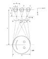
本発明に係るセキュリティ媒体の実施形態について図を用いて詳細に説明する。図1は、本発明の実施形態に係るセキュリティ媒体を有するセキュリティカードを示す斜視図である。セキュリティ媒体は、クレジットカードやID証、紙幣、金券、有価証券など真贋判定が必要とされる各種カード、紙類などに形成される媒体であって、容易に複製を作製することができないことが必要とされる。 An embodiment of a security medium according to the present invention will be described in detail with reference to the drawings. FIG. 1 is a perspective view showing a security card having a security medium according to an embodiment of the present invention. The security medium is a medium formed on various cards, papers, etc. that require authenticity determination such as credit cards, ID certificates, banknotes, cash vouchers, securities, etc., and may not be easily duplicated. Needed.
図1に示すセキュリティ媒体5は、クレジットカードのようなセキュリティカード4に設けられた例であって、セキュリティカード4の一部に所定の像が目視可能に形成されている。セキュリティカード4を使用もしくは認証する者は、セキュリティ媒体5に予め定められている像が表示されていることをもって真のセキュリティカード4であることを認証する。以後の説明では、図1に示すように、セキュリティカード4の板面をXY平面にとり、XY平面に垂直かつ使用者が観察する方向をZ軸の正の方向にとって説明する。
The
図2は、本発明の実施形態に係るセキュリティ媒体(タイプA)の構成を示す模式図であって、セキュリティ媒体の一部を拡大した斜視図となっている。本実施形態のセキュリティ媒体5は、XY平面に平行な面上に配列された3次元微細構造物1と、XY平面に平行な面上に配列されたマイクロレンズ2によって、拡大された3次元微細構造物1の実像もしくは虚像を観察者に観察させる。これは隣接する3次元微細構造物1間の間隔(ピッチw)と隣接するマイクロレンズ2の間隔(ピッチp)の間にわずかなピッチ差を設け、ピッチ差によって発生するモアレ効果を利用したものとなっている。
FIG. 2 is a schematic view showing the configuration of the security medium (type A) according to the embodiment of the present invention, and is a perspective view in which a part of the security medium is enlarged. The
図3には、図2に記載する3次元微細構造物1のXY平面に平行な面における配列(3次元微細構造物アレイ)、マイクロレンズ2のXY平面に平行な面における配列(マイクロレンズアレイ)が、それぞれ図3(a)、(b)に示されている。本実施形態の3次元微細構造物1、マイクロレンズ2の配列は、どちらも格子状に配列されたものとなっている。図3(a)に示されるように隣接する3次元微細構造物1はX軸方向にピッチw、Y軸方向にピッチzを有して配列されている。ピッチwとピッチzを等距離としてもよい。3次元微細構造物1の形状は、任意な形状とすることができるが、後ほど説明する拡大率の関係を分かりやすくするため、直径hで円形の外形を有するものとしている。
FIG. 3 shows an arrangement on the plane parallel to the XY plane of the three-dimensional microstructure 1 shown in FIG. 2 (three-dimensional microstructure array), and an arrangement on the plane parallel to the XY plane of the microlens 2 (microlens array). ) Are shown in FIGS. 3 (a) and 3 (b), respectively. In the present embodiment, the three-dimensional microstructure 1 and the
一方、図3(b)に示されるようにマイクロレンズ2は、3次元微細構造物1と同様に格子状に配列されている。そして隣接するマイクロレンズ2は、X軸方向にピッチp、Y軸方向にピッチqを有して配列されている。ただし、このピッチpは3次元微細構造物1のピッチwに対して僅かな差(ピッチ差)を有したものとなっている。また、ピッチqは3次元微細構造物1のピッチzに対して僅かな差(ピッチ差)を有したものとなっている。このピッチpとピッチqも等距離としてもよい。
On the other hand, as shown in FIG. 3B, the
マイクロレンズ2の大きさは、数十〜数百μm程度の大きさに形成される。一方、マイクロレンズ2によって拡大される3次元微細構造物1は、マイクロレンズ2の大きさよりも小さく形成されることとなる。3次元微細構造物1は、秘匿性の都合上、直接目視したときに視認できない程度の大きさとすることが好ましい。
The
3次元微細構造物1とマイクロレンズ2の配列は、図3のような格子状配列に限らず、例えば、図4のような配列であってもよい。図4の例は、3次元微細構造物1、マイクロレンズ2が亀甲状に配列された例である。図4(a)に示されるように、X軸方向に隣接する3次元微細構造物1は、ピッチwを有して配列される。そして、斜め方向に隣接する3次元微細構造物1に対してもピッチwを有して配列されている。マイクロレンズ2も同様であって、図4(b)に示されるようにX軸方向、斜め方向に隣接するマイクロレンズ2間はピッチpを有して配列されている。本実施形態のセキュリティ媒体は、モアレ効果を利用することで複数の3次元微細構造物1の拡大表示像を重ねて観察者に提示することとしている。そのため、単位面積あたりに配置された3次元微細構造物1やマイクロレンズ2が多いほど、表示像を鮮明なものとすることが可能となる。
The arrangement of the three-dimensional microstructure 1 and the
では、図2に示した構成のセキュリティ媒体(タイプA)について、その表示原理を図5を用いて説明する。ここではX軸方向に隣接する3次元微細構造物1による表示原理を説明するが、Y軸方向、あるいは、斜め方向に隣接する3次元微細構造物1に対しても同様の表示原理を利用することで、表示像をより鮮明なものとすることが可能となる。 The display principle of the security medium (type A) having the configuration shown in FIG. 2 will be described with reference to FIG. Here, the display principle by the three-dimensional microstructure 1 adjacent in the X-axis direction will be described, but the same display principle is also used for the three-dimensional microstructure 1 adjacent in the Y-axis direction or oblique direction. As a result, the display image can be made clearer.
タイプAのセキュリティ媒体は、観察者側に近い側にマイクロレンズ2のレンズ面が配置され、観察者から遠い側に3次元微細構造物1が配置されたレイアウトとされている。図5には、マイクロレンズ2によって形成されるレンズ面と、3次元微細構造物1、並びに観察される実像が模式的に示されている。
The type A security medium has a layout in which the lens surface of the
3次元微細構造物1は、Z軸方向すなわち観察者の観察方向において、マイクロレンズ2の略焦点位置に配置される。略焦点位置とは、観察者が拡大された3次元微細構造物1を視認できる範囲の位置を意味するものであって、正確な焦点距離に対し約30%範囲以内の位置のことをいう。隣接するマイクロレンズ2間のピッチをp、隣接する3次元微細構造物1間のピッチをw、3次元微細構造物1の直径をh、マイクロレンズ2の曲率半径の中心位置から3次元微細構造物1までの距離をd、3次元微細構造物1の実像とマイクロレンズ2の曲率半径の中心位置までの距離をL、観察される実像の直径をHとする。なお、図はZX平面内での主光線の様子を示したものとなっているが、拡大の様子を分かりやすくするため、3次元微細構造物1とその実像については各XY平面上の様子を示したものとしている。図2で説明したように、観察者は、Z軸の正方向を観察方向としてセキュリティ媒体の観察することで、拡大された3次元微細構造物1の像を観察することが可能とされる。
The three-dimensional microstructure 1 is arranged at a substantially focal position of the
図5のセキュリティ媒体の構成は、マイクロレンズ2のピッチpよりも3次元微細構造物1のピッチwが大きい場合(w>p)の構成となっている。この場合、3次元微細構造物1は、マイクロレンズ2によって拡大像を形成する。所定の距離Lの位置では、ピッチ差(w−p)を起因として、隣接する拡大像が同じ位置あるいは略同じ位置に重なり合うことで実像を形成、すなわち、セキュリティ媒体に対して観察者側に像が形成される。これはいわゆるモアレ効果を利用したものであって、観察者は拡大された3次元微細構造物1を浮いた状態で観察することが可能となる。
The configuration of the security medium in FIG. 5 is a configuration when the pitch w of the three-dimensional microstructure 1 is larger than the pitch p of the microlenses 2 (w> p). In this case, the three-dimensional microstructure 1 forms an enlarged image by the
このように拡大して観察される3次元微細構造物1の拡大率について検証しておく。図5において幾何学上の相似関係から(1−1)式を導くことができる。
w/(L+d)=p/L ・・・(1−1)
(1−1)式を変形すると、
L=dp/(w−p) ・・・(1−2)
The enlargement rate of the three-dimensional microstructure 1 observed in this way is verified. In FIG. 5, the equation (1-1) can be derived from the geometric similarity.
w / (L + d) = p / L (1-1)
When formula (1-1) is transformed,
L = dp / (w−p) (1-2)
同様に、幾何学上の相似関係から(1−3)式を導くことができる。
H=Lh/d ・・・(1−3)
(1−3)式を変形すると、
L=Hd/h ・・・(1−4)
Similarly, the expression (1-3) can be derived from the geometric similarity.
H = Lh / d (1-3)
When the equation (1-3) is transformed,
L = Hd / h (1-4)
(1−2)式と(1−4)式から、観察される3次元微細構造物1の拡大率αは(1−5)式にて表すことができる。
α=H/h=p/(w−p)・・・(1−5)
From the formulas (1-2) and (1-4), the magnification α of the observed three-dimensional microstructure 1 can be expressed by the formula (1-5).
α = H / h = p / (w−p) (1-5)
以下に、図5のセキュリティ媒体について、拡大率αと観察される像の大きさHの数値実施例を記載しておく。何れの場合も3次元微細構造物1の大きさh(直径)を90μm、3次元微細構造物のピッチwを98.9μmに固定している。 In the following, numerical examples of the enlargement ratio α and the observed image size H are described for the security medium of FIG. In any case, the size h (diameter) of the three-dimensional microstructure 1 is fixed at 90 μm, and the pitch w of the three-dimensional microstructure is fixed at 98.9 μm.
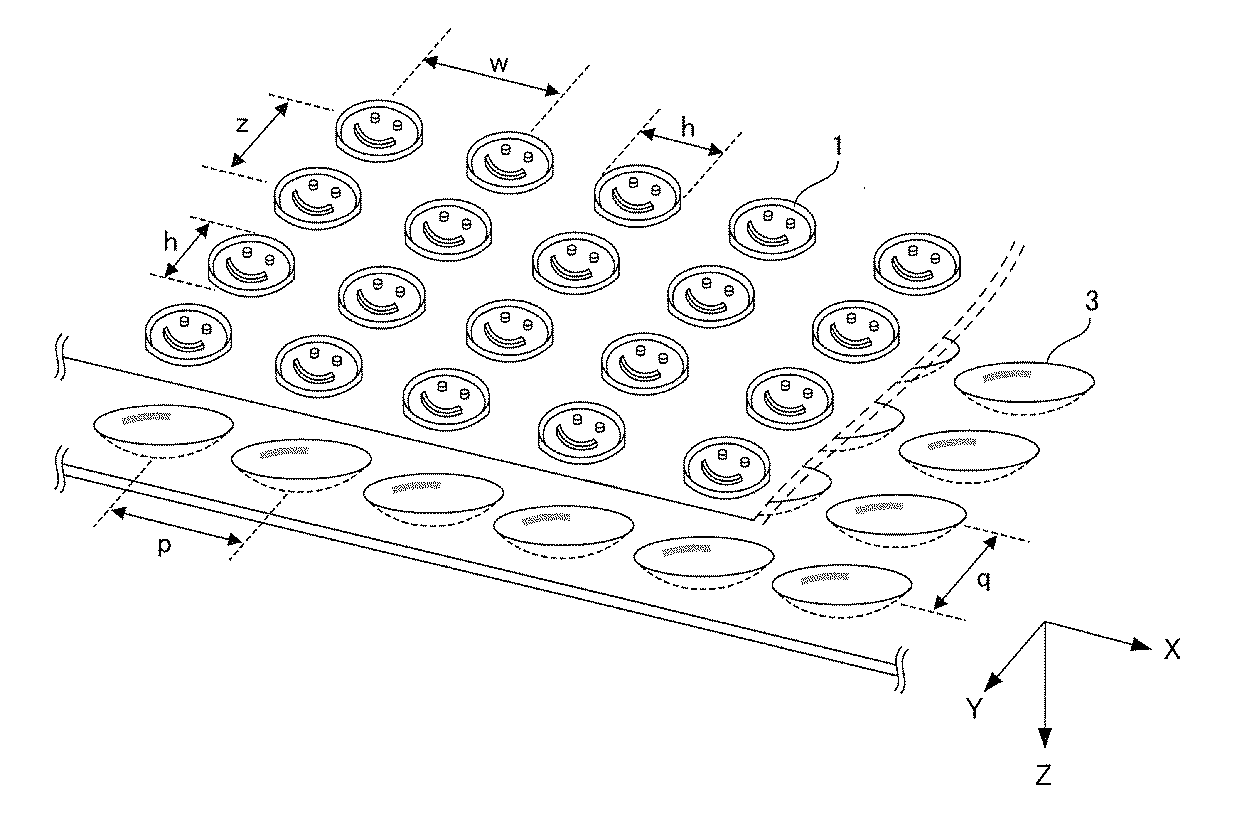
表1から分かるようにピッチ差が小さくなるほど、拡大率α、観察像の大きさは共に大きくなることが分かる。また、1μmのピッチ差が拡大率に大きく影響を及ぼすこともみてとれる。3次元微細構造物1とマイクロレンズ2とのピッチ差を精密に異ならせて製造することは難しいため、その複製を困難な状態とし、容易に偽造や模造を行うことを防止することが可能となる。
As can be seen from Table 1, the smaller the pitch difference, the larger the enlargement ratio α and the size of the observation image. It can also be seen that a pitch difference of 1 μm greatly affects the enlargement ratio. Since it is difficult to manufacture the three-dimensional fine structure 1 and the
図6は、図5と同様、観察者側にマイクロレンズ2が配置されているセキュリティ媒体(タイプA)であって、3次元微細構造物1のピッチwよりもマイクロレンズ2のピッチpが大きい場合(p>w)の構成となっている。図6には、マイクロレンズ2によって形成されるレンズ面と、3次元微細構造物1、並びに観察される虚像が模式的に示されている。
FIG. 6 shows a security medium (type A) in which the
3次元微細構造物1は、観察者の観察方向において、マイクロレンズ2の略焦点位置に配置される。略焦点位置とは、観察者が拡大された3次元微細構造物1を視認できる範囲の位置を意味するものであって、正確な焦点距離に対し約30%範囲以内の位置のことをいう。隣接するマイクロレンズ2間のピッチをp、隣接する3次元微細構造物1間のピッチをw、3次元微細構造物1の直径をh、マイクロレンズ2の曲率半径の中心位置から3次元微細構造物1までの距離をd、3次元微細構造物1から実像までの距離をL、観察される実像の直径をHとする。
The three-dimensional microstructure 1 is disposed at a substantially focal position of the
この場合、3次元微細構造物1は、マイクロレンズ2によって拡大像を形成する。このとき所定の距離Lの位置では、ピッチ差(p−w)を起因として、隣接する拡大像が同じ位置あるいは略同じ位置に重なり合うことで虚像を形成する。すなわち、セキュリティ媒体に対して観察者と反対側に像を形成する。観察者は拡大された3次元微細構造物1を沈んだ状態で観察することが可能となる。
In this case, the three-dimensional microstructure 1 forms an enlarged image by the
このように拡大して観察される3次元微細構造物1の拡大率について検証しておく。図6において幾何学上の相似関係から(2−1)式を導くことができる。
w/L=p/(L+d) ・・・(2−1)
(2−1)式を変形すると、
L=dw/(p−w) ・・・(2−2)
The enlargement rate of the three-dimensional microstructure 1 observed in this way is verified. In FIG. 6, the equation (2-1) can be derived from the geometric similarity.
w / L = p / (L + d) (2-1)
When the equation (2-1) is transformed,
L = dw / (p−w) (2-2)
同様に、幾何学上の相似関係から(2−3)式を導くことができる。
d/h=(d+L)/H ・・・(2−3)
(2−3)式を変形すると、
L=d(H/h−1) ・・・(2−4)
Similarly, equation (2-3) can be derived from the geometric similarity.
d / h = (d + L) / H (2-3)
When the equation (2-3) is transformed,
L = d (H / h-1) (2-4)
(2−2)式と(2−4)式から、観察される3次元微細構造物1の拡大率αは(2−5)式にて表すことができる。
α=H/h=p/(p−w)・・・(2−5)
From the formulas (2-2) and (2-4), the magnification α of the observed three-dimensional microstructure 1 can be expressed by the formula (2-5).
α = H / h = p / (p−w) (2-5)
図2に示されるようなタイプAのセキュリティ媒体では、観察者側に配列されたマイクロレンズ2を介して、観察側に対して反対側(観察者側からみて遠い側)に配列された3次元微細構造物の実像あるいは虚像を拡大観察することが可能とされている。本実施形態のセキュリティ媒体は、このような構成(タイプA)のみならず、次のような構成(タイプB)を採用することもできる。
In the type A security medium as shown in FIG. 2, the three-dimensional array is arranged on the opposite side (the side far from the observer side) through the
図7は、本発明の実施形態に係るセキュリティ媒体(タイプB)の構成を示す模式図であって、セキュリティ媒体の一部を拡大した斜視図となっている。本実施形態のセキュリティ媒体5は、XY平面に平行な面上に配列された3次元微細構造物1と、XY平面に平行な面上に配列されたマイクロミラーレンズ3によって、拡大された3次元微細構造物1の実像もしくは虚像を観察者に観察させることを可能としている。
FIG. 7 is a schematic diagram showing the configuration of the security medium (type B) according to the embodiment of the present invention, and is a perspective view in which a part of the security medium is enlarged. The
3次元微細構造物1の配列(3次元微細構造物アレイ)、マイクロミラーレンズ3の配列(マイクロミラーレンズアレイ)は、図7、図3に示すように格子状あるいは図4で説明したように亀甲状にて配置される。本実施形態の3次元微細構造物1並びにそれが配置されたシートは透明部材によって構成されている。一方、マイクロミラーレンズ3は、Z軸負の方向に凹面を向けた反射面を有し、観察方向(Z軸負側から正側に向かう方向)から入射する光を反射させる。マイクロミラーレンズ3で反射された光は、3次元微細構造物1を透過し、観察者に対して3次元微細構造物1の実像もしくは虚像を拡大表示する。
The arrangement of the three-dimensional microstructure 1 (three-dimensional microstructure array) and the arrangement of the micromirror lens 3 (micromirror lens array) are as shown in FIG. 7 and FIG. It is arranged in a turtle shell shape. The three-dimensional microstructure 1 of this embodiment and the sheet on which it is arranged are constituted by a transparent member. On the other hand, the
図8は、観察者側に3次元微細構造物1が配置されたセキュリティ媒体(タイプB)であって、3次元微細構造物1のピッチwよりもマイクロミラーレンズ3のピッチpが大きい場合(p>w)の構成となっている。図8には、マイクロミラーレンズ3によって形成されるミラー面と、3次元微細構造物1、並びに観察される実像が模式的に示されている。
FIG. 8 shows a security medium (type B) in which the three-dimensional microstructure 1 is arranged on the viewer side, and the pitch p of the
3次元微細構造物1は、観察者の観察方向において、マイクロミラーレンズ3の略焦点位置に配置される。略焦点位置とは、観察者が拡大された3次元微細構造物1を視認できる範囲の位置を意味するものであって、正確な焦点距離に対し約30%範囲以内の位置のことをいう。隣接するマイクロミラーレンズ3間のピッチをp、隣接する3次元微細構造物1間のピッチをw、3次元微細構造物1の直径をh、マイクロミラーレンズ3の曲率半径の中心位置から3次元微細構造物1までの距離をd、3次元微細構造物1からその実像までの距離をL、観察される実像の直径をHとする。図7に示されるように、観察者は、Z軸の正方向を観察方向としてセキュリティ媒体の観察することで、拡大された3次元微細構造物1の像を観察することが可能とされる。
The three-dimensional microstructure 1 is disposed at a substantially focal position of the
この場合、マイクロミラーレンズ3から射出される反射光は、3次元微細構造物1を透過して拡大像を形成する。このとき所定の距離Lの位置では、ピッチ差(p−w)を起因として、隣接する拡大像が同じ位置あるいは略同じ位置に重なり合うことで実像を形成する。これもタイプAのセキュリティ媒体と同様、モアレ効果を利用したものであって、観察者は、拡大された3次元微細構造物1を浮いた状態で観察することが可能となる。
In this case, the reflected light emitted from the
このように拡大して観察される3次元微細構造物1の拡大率について検証しておく。図8において幾何学上の相似関係から(3−1)式を導くことができる。
w/L=p/(L+d) ・・・(3−1)
(2−1)式を変形すると、
L=dw/(p−w) ・・・(3−2)
The enlargement rate of the three-dimensional microstructure 1 observed in this way is verified. In FIG. 8, the equation (3-1) can be derived from the geometric similarity.
w / L = p / (L + d) (3-1)
When the equation (2-1) is transformed,
L = dw / (p−w) (3-2)
同様に、幾何学上の相似関係から(3−3)式を導くことができる。
d/h=(d+L)/H ・・・(3−3)
(2−3)式を変形すると、
L=d(H/h−1) ・・・(3−4)
Similarly, the expression (3-3) can be derived from the geometric similarity.
d / h = (d + L) / H (3-3)
When the equation (2-3) is transformed,
L = d (H / h-1) (3-4)
(3−2)式と(3−4)式から、観察される3次元微細構造物1の拡大率αは(3−5)式にて表すことができる。
α=H/h=p/(p−w)・・・(3−5)
From the expressions (3-2) and (3-4), the magnification α of the observed three-dimensional microstructure 1 can be expressed by the expression (3-5).
α = H / h = p / (p−w) (3-5)
一方、図9は、図8と同様、観察者側に3次元微細構造物1が配置されているセキュリティ媒体(タイプB)であって、マイクロミラーレンズ3のピッチpよりも3次元微細構造物1のピッチwが大きい場合(w>p)の構成となっている。図9には、マイクロミラーレンズ3によって形成されるミラー面と、3次元微細構造物1、並びに観察される虚像が模式的に示されている。
On the other hand, FIG. 9 shows a security medium (type B) in which the three-dimensional fine structure 1 is arranged on the viewer side as in FIG. 8, and the three-dimensional fine structure is larger than the pitch p of the
3次元微細構造物1は、観察者の観察方向において、マイクロミラーレンズ3の略焦点位置に配置される。略焦点位置とは、観察者が拡大された3次元微細構造物1を視認できる範囲の位置を意味するものであって、正確な焦点距離に対し約30%範囲以内の位置のことをいう。隣接するマイクロミラーレンズミラー3間のピッチをp、隣接する3次元微細構造物1間のピッチをw、3次元微細構造物1の直径をh、マイクロミラーレンズミラー3の曲率半径の中心位置から3次元微細構造物1までの距離をd、3次元微細構造物1からその虚像までの距離をLとする。
The three-dimensional microstructure 1 is disposed at a substantially focal position of the
この場合、マイクロミラーレンズ3から射出された反射光は、3次元微細構造物1を透過して拡大像を形成する。所定の距離Lの位置では、ピッチ差(w−p)を起因として、隣接する拡大像が同じ位置あるいは略同じ位置に重なり合うことで虚像を形成する。観察者は拡大された3次元微細構造物1を沈んだ状態で観察することが可能となる。
In this case, the reflected light emitted from the
このように拡大して観察される3次元微細構造物1の拡大率について検証しておく。図9において幾何学上の相似関係から(4−1)式を導くことができる。
w/L=p/(L−d) ・・・(4−1)
(1−1)式を変形すると、
L=dw(w−p) ・・・(4−2)
The enlargement rate of the three-dimensional microstructure 1 observed in this way is verified. In FIG. 9, the equation (4-1) can be derived from the geometric similarity.
w / L = p / (L−d) (4-1)
When formula (1-1) is transformed,
L = dw (w−p) (4-2)
同様に、幾何学上の相似関係から(4−3)式を導くことができる。
h/d=H/(L−d) ・・・(4−3)
(4−3)式を変形すると、
L=d(H/h+1) ・・・(4−4)
Similarly, equation (4-3) can be derived from the geometric similarity.
h / d = H / (L−d) (4-3)
When the equation (4-3) is transformed,
L = d (H / h + 1) (4-4)
(4−2)式と(4−4)式から、観察される3次元微細構造物1の拡大率αは(4−5)式にて表すことができる。
α=H/h=p/(p−w) ・・・(4−5)
From the expressions (4-2) and (4-4), the magnification α of the observed three-dimensional microstructure 1 can be expressed by the expression (4-5).
α = H / h = p / (p−w) (4-5)
タイプA、タイプBのセキュリティ媒体それぞれについて、w>pの場合と、w<pの場合の拡大率について検討したが、次にw>pの場合(ケース1)、w<pの場合(ケース2)のそれぞれについて、3次元微細構造物のピッチwの好適とされる範囲について検討する。ここではマイクロレンズ2を使用したタイプAについて検討するが、マイクロミラーレンズ3を用いたタイプBについても同様である。
For each of the type A and type B security media, we examined the enlargement ratio when w> p and when w <p. Next, when w> p (case 1), when w <p (case) For each of 2), the preferred range of the pitch w of the three-dimensional microstructure will be examined. Here, type A using the
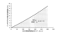
まず、w>pの場合(ケース1)について3次元微細構造物1のピッチwの上限、下限について説明する。
3次元微細構造物1のピッチwに対するピッチ差(w−p)の比率をA[%]とすると、
3次元微細構造物1のピッチwに対するマイクロレンズ2のピッチpとのピッチ差は、
w−p=w×A/100 ・・・(5−1)
で表すことができる。このピッチ差を用いてマイクロレンズ2のピッチpは、
p=w(1−A/100) ・・・(5−2)
と表すことができる。
First, an upper limit and a lower limit of the pitch w of the three-dimensional microstructure 1 will be described in the case of w> p (case 1).
When the ratio of the pitch difference (w−p) to the pitch w of the three-dimensional microstructure 1 is A [%],
The pitch difference between the pitch w of the
w−p = w × A / 100 (5-1)
Can be expressed as Using this pitch difference, the pitch p of the
p = w (1-A / 100) (5-2)
It can be expressed as.
ケース1の場合、拡大率αは(1−5)式で表すことができる。ピッチw内に位置する3次元微細構造物1は、ピッチwと拡大率αの積となる大きさβを上限として観察されることとなる。
β=w×α=w(p/w−p) ・・・(5−3)
In case 1, the enlargement ratio α can be expressed by equation (1-5). The three-dimensional microstructure 1 located in the pitch w is observed with the size β, which is the product of the pitch w and the magnification factor α, as the upper limit.
β = w × α = w (p / w−p) (5-3)
観察時における大きさβを2000[μm](2[mm])以上の大きさに設定することを考えると(5−3)式から
w(p/w−p)≧2000 ・・・(5−3)'
の関係が必要となる。(5−3)'式に(5−2)式を代入すると、
100w/(2000+w)≧A ・・・(5−3)''
なる関係が得られ、3次元微細構造物1のピッチwに対するピッチ差(w−p)の比率Aは、3次元微細構造物1のピッチwに依存することが分かる。
Considering that the size β at the time of observation is set to 2000 [μm] (2 [mm]) or more, from the equation (5-3), w (p / wp) ≧ 2000 (5 -3) '
This relationship is required. Substituting equation (5-2) into equation (5-3) ',
100w / (2000 + w) ≧ A (5-3) ''
It can be seen that the ratio A of the pitch difference (w−p) to the pitch w of the three-dimensional microstructure 1 depends on the pitch w of the three-dimensional microstructure 1.
図10は、(5−3)''をグラフ化した図であって、w>pの場合(ケース1)における3次元微細構造物のピッチwと、ピッチwに対するピッチ差(w−p)の比率Aを示した図である。実線は(5−3)''において、大きさβがちょうど2000[μm]となる値を示している。この実線よりも下方、図ではドットが付された領域内では大きさβ
は2000[μm]よりも大きい値となる。
FIG. 10 is a graph of (5-3) ″, and the pitch w of the three-dimensional microstructure in the case of w> p (case 1) and the pitch difference (w−p) with respect to the pitch w. FIG. The solid line indicates the value at which the size β is exactly 2000 [μm] at (5-3) ″. Below this solid line, in the figure the size β
Becomes a value larger than 2000 [μm].
3次元微細構造物1のピッチwの上限は300[μm]以下に設定することが好ましい。3次元微細構造物1のピッチwを300[μm]以上とすると、レンズ等の拡大手段を用いなくてもピッチw内に配置される3次元構造物1を目視で容易に観察可能となる。したがって、偽造や模造を防止する上では目視で観察できない大きさにピッチwを設けることが好ましい。さらに好ましくは、ピッチwの上限を100[μm]に設定することとする。目視での観察をより困難な状態とし、偽造、模造をさらに抑制することが可能となる。 The upper limit of the pitch w of the three-dimensional microstructure 1 is preferably set to 300 [μm] or less. When the pitch w of the three-dimensional fine structure 1 is set to 300 [μm] or more, the three-dimensional structure 1 arranged in the pitch w can be easily observed visually without using a magnifying means such as a lens. Therefore, it is preferable to provide the pitch w in a size that cannot be visually observed in order to prevent forgery or imitation. More preferably, the upper limit of the pitch w is set to 100 [μm]. Visual observation can be made more difficult, and counterfeiting and imitation can be further suppressed.
一方、マイクロレンズ2のピッチpは、3次元微細構造物1のピッチwと同様に300[μm]以下とすることが好ましく、100[μm]以下の大きさに設定することがさらに好ましい。観察される実像または虚像は1個のマイクロレンズ2を1画素として観察される。ピッチpが300[μm]以上になると画素が粗くなり解像度の低い観察像となってしまう。一方、ピッチpが100[μm]以下では画素が目視でほとんど見えなくなり解像度の高い像を提供することが可能となる。
On the other hand, the pitch p of the
また3次元微細構造物1のピッチwの下限は10[μm]とすることが好ましい。これは、ピッチ差(w−p)の比率Aを理由とするものである。本実施形態ではモアレ効果を利用して像を拡大する関係上、3次元微細構造物1とマイクロレンズ2のピッチ差が重要である。しかしながら、ピッチ差の比率Aは0.5[%]以上の精度で合わせ込むことは困難である。したがって、3次元微細構造物1のピッチwの下限は、β=2000[μm]におけるピッチ差の比率A=0.5[%]としたときの値である10[μm]に設定することが好ましい。
The lower limit of the pitch w of the three-dimensional microstructure 1 is preferably 10 [μm]. This is because of the ratio A of the pitch difference (w−p). In the present embodiment, the pitch difference between the three-dimensional microstructure 1 and the
次に、w<pの場合(ケース2)について3次元微細構造物1のピッチwの上限、下限について説明する。
3次元微細構造物1のピッチwに対するピッチ差(p−w)の比率をA[%]とすると、
3次元微細構造物1のピッチwに対するマイクロレンズ2のピッチpとのピッチ差は、
p−w=w×A/100 ・・・(6−1)
で表すことができる。このピッチ差を用いてマイクロレンズ2のピッチpは、
p=w(1+A/100) ・・・(6−2)
と表すことができる。
Next, an upper limit and a lower limit of the pitch w of the three-dimensional microstructure 1 will be described in the case of w <p (case 2).
When the ratio of the pitch difference (p−w) to the pitch w of the three-dimensional microstructure 1 is A [%],
The pitch difference between the pitch w of the
p−w = w × A / 100 (6-1)
Can be expressed as Using this pitch difference, the pitch p of the
p = w (1 + A / 100) (6-2)
It can be expressed as.
ケース2の場合、拡大率αは(2−5)式で表すことができる。ピッチw内に位置する3次元微細構造物1は、ピッチwと拡大率αの積となる大きさβを上限として観察されることとなる。
β=w×α=w(p/p−w) ・・・(6−3)
In
β = w × α = w (p / p−w) (6-3)
観察時における大きさβを2000[μm](2[mm])以上の大きさに設定することを考えると(6−3)式から
w(p/p−w)≧2000 ・・・(6−3)'
の関係が必要となる。(6−3)'式に(6−2)式を代入すると、
100w/(2000−w)≧A ・・・(6−3)''
なる関係が得られ、3次元微細構造物1に対するピッチ差(p−w)の比率Aは、ケース1の場合と同様、3次元微細構造物1のピッチwに依存することが分かる。
Considering that the size β at the time of observation is set to 2000 [μm] (2 [mm]) or more, from the equation (6-3), w (p / p−w) ≧ 2000 (6 -3) '
This relationship is required. Substituting (6-2) into (6-3) ',
100w / (2000-w) ≧ A (6-3) ''
It can be seen that the ratio A of the pitch difference (p−w) with respect to the three-dimensional microstructure 1 depends on the pitch w of the three-dimensional microstructure 1 as in the case 1.
図11は、(6−3)''をグラフ化した図であって、w<pの場合(ケース2)における3次元微細構造物のピッチwと、ピッチwに対するピッチ差(p−w)の比率Aを示した図である。実線は(6−3)''において、大きさβがちょうど2000[μm]となる値を示している。この実線よりも下方、図ではドットが付された領域内では大きさβは2000[μm]よりも大きい値となる。 FIG. 11 is a graph of (6-3) ″, and the pitch w of the three-dimensional microstructure in the case of w <p (case 2) and the pitch difference (p−w) with respect to the pitch w. FIG. The solid line indicates the value at which the size β is exactly 2000 [μm] at (6-3) ″. Below the solid line, in the drawing, in the region with dots, the size β is greater than 2000 [μm].
ケース1の場合と同様、3次元微細構造物1のピッチwの上限は、偽造や模造抑制の観
点から300[μm]以下に設定することが好ましい。さらには100[μm]に設定す
ることが好ましい。
As in the case 1, the upper limit of the pitch w of the three-dimensional microstructure 1 is preferably set to 300 [μm] or less from the viewpoint of counterfeiting and counterfeiting. Furthermore, it is preferable to set to 100 [μm].
また、ケース1の場合と同様、マイクロレンズ2のピッチpについては、300[μm]以下の大きさに設定することが好ましく、100[μm]以下の大きさに設定することがさらに好ましい。
Similarly to the case 1, the pitch p of the
また、ケース2の場合、3次元微細構造物1のピッチwの下限は10[μm]とすることが好ましい。これはケース1の場合と同様、ピッチ差の比率Aを0.5[%]以上に合わせ込むことが困難であることを理由としている。したがって、3次元微細構造物1のピッチwの下限は、β=2000[μm]におけるピッチ差の比率A=0.5[%]としたときの値である10[μm]に設定することが好ましい。
In the
では、本発明の実施形態に係るセキュリティ媒体の製造過程(製造方法)、並びに、その構成の実施例を説明する。 Now, an example of a security medium manufacturing process (manufacturing method) and a configuration thereof according to the embodiment of the present invention will be described.
(実施例1)
図12には、セキュリティ媒体(タイプA)の製造過程及びその構成が示されている。
図12(a)、(b)はセキュリティ媒体の製造過程を、また、図12(c)は完成したセキュリティ媒体を被着体33に貼着したときの構成(図1におけるA−A'間のZX平面での断面図)が示されている。なお、図1において実際に利用可能なセキュリティカード4を構成する場合、図12に図示した以外の層が設けられる場合がある。
Example 1
FIG. 12 shows the manufacturing process and configuration of the security medium (type A).
12A and 12B show the manufacturing process of the security medium, and FIG. 12C shows the configuration when the completed security medium is attached to the adherend 33 (between AA ′ in FIG. 1). Of the ZX plane). In the case where the
工程1:Si基板の上にポジレジスト(東京応化工業社製PMER P−LA900PM)を10μmの膜厚で塗布し、フォトマスクを介して、ステッパ露光、現像処理、ポストベークを施し、1つ90μmの大きさ(凹凸方向の深さ約4μm)の凹凸パターンを有する3次元微細構造物を20mm×20mmのエリア内にX方向99μm、Y方向99μmピッチで配列した3次元微細構造物1の原版(金型50)を作製する。 Step 1: A positive resist (PMER P-LA900PM manufactured by Tokyo Ohka Kogyo Co., Ltd.) is applied on a Si substrate with a film thickness of 10 μm, and is subjected to stepper exposure, development processing, and post-baking through a photomask, one by 90 μm. A master plate of a three-dimensional microstructure 1 in which three-dimensional microstructures having a concavo-convex pattern having a size of (a depth of about 4 μm in the concavo-convex direction) are arranged in a 20 mm × 20 mm area at a pitch of 99 μm in the X direction and 99 μm in the Y direction A mold 50) is produced.
工程2:150mm×150mmの大きさのSUS板の表面に版面形成用の銅めっき層を設け、銅めっき層にエッチングによってマイクロレンズを形成後、クロムめっきを施して、20mm×20mmのエリア内にX方向100μm、Y方向100μmピッチで配列したマイクロレンズ2の原版(金型51)を作製する。
Step 2: A copper plating layer for forming a plate surface is provided on the surface of a SUS plate having a size of 150 mm × 150 mm, a microlens is formed on the copper plating layer by etching, and then chromium plating is performed, so that an area of 20 mm × 20 mm is formed. An original plate (mold 51) of the
工程3:プラスチックシートなど熱可塑性を有する1枚の基材41の両側に、工程1と工程2で作製した原版(金型50、51)が対面になるように配置して熱プレスすることで、基材41の両面に3次元微細構造1とマイクロレンズ2が賦形される。熱プレスを行う際、2枚の原版(金型50、51)の位置合わせを行うことで、基材41上に形成される3次元微細構造物1とマイクロレンズ2の位置合わせを容易にするとともに、位置合わせの精度の向上を図ることが可能となる。また、本実施例のように熱プレスを用いて形成する場合、熱による基材41の収縮あるいは膨張の影響が3次元微細構造物1側とマイクロレンズ2側で異なることがなく、完成後の両者の位置合わせの精度の向上を図ることが可能となる。
Step 3: On the both sides of one
工程4:工程3で作製した複製版の3次元微細構造の表面(観察する方向と逆側)に反射層42を形成する。本実施形態では、Al(アルミ)を約50nmスパッタすることで3次元微細構造物1の表面に反射層42を形成している。このようにマイクロレンズ2と3次元微細構造物1が1枚の基材41(シート)に設けられた形態では、3次元微細構造物1に対し、観察側とは反対側の表面に反射層42が設けたことで、3次元微細構造物1の原版(金型50)によって形成された形状を直接観察することが可能であり、観察者は、賦形時における3次元微細構造物1の形を観察することとなり、エッジ鈍り等を抑えた先鋭な形状を観察することが可能となる。
Step 4: A
工程5:反射層42側にヒートシール61を約5μm塗布し、有価証券などの被着体33に貼付可能な構成としている。
Step 5: About 5 μm of
工程6:工程5の中のマイクロレンズアレイと3次元微細構造のパターン部分を15mm×15mmで打ち抜くことで、貼付可能なラベル形態としてのセキュリティ媒体が完成する。
Step 6: The microlens array and the pattern portion of the three-dimensional fine structure in
図12(c)は、このような工程で完成したセキュリティ媒体を有価証券などの被着体33に貼着した状態が示されている。セキュリティ媒体のマイクロレンズ2を介して3次元微細構造物1を観察することで、拡大された3次元微細構造物1を観察することが可能となる。
FIG. 12 (c) shows a state in which the security medium completed in such a process is attached to an
以上、実施例1では、熱可塑性を有する基材41を用いて形成されたセキュリティ媒体を被着体33に貼着する形態について説明したが、図12(b)の貼着前の形態を使用形態とすることも可能である。基材41の表面もしくは裏面、あるは両面に対して、絵柄や個人情報を印刷することで、ID証あるいはポリマー紙幣等として使用することが可能となる。
As mentioned above, although Example 1 demonstrated the form which sticks the security medium formed using the
(実施例2)
図13には本発明の実施形態に係るセキュリティ媒体(タイプB)の別の構成が示されている。製造過程は実施例1とほぼ同様であって、熱可塑性を有する基材41を、2つの原版(金型)で熱プレスすることで基材41の一面に3次元微細構造物1が、他面にマイクロミラーレンズ3が形成される。本実施形態においても1枚のシート(基材41)に同時に3次元微細構造物1、マイクロミラーレンズ3を形成することで、その位置合わせの精度向上を図ることを可能としている。また、熱プレスを行う際には、シートの両面での熱影響を同等にすることで、3次元微細構造物1、マイクロレンズ2の位置合わせの精度向上が図られる。
(Example 2)
FIG. 13 shows another configuration of the security medium (type B) according to the embodiment of the present invention. The manufacturing process is substantially the same as in Example 1, and the three-dimensional microstructure 1 is formed on one surface of the
このタイプBのセキュリティ媒体では、マイクロミラーレンズ3で反射された光にて3次元微細構造物1が拡大されるとともに、拡大された3次元微細構造物1を重ねるモアレ効果を利用することで、拡大された3次元微細構造物1の像を観察者に提示することが可能となる。
In this type B security medium, the three-dimensional microstructure 1 is magnified by the light reflected by the
また、実施例2のセキュリティ媒体では、マイクロミラーレンズ3の表面、すなわち、観察側とは反対側に反射層42が設けられることで、設計時の反射光光路を略再現することが可能となり、歪みの少ない3次元微細構造物1の像を観察者に提示することを可能としている。
Further, in the security medium of Example 2, the
以上、実施例1、2では1枚のシート(熱可塑性を有する基材41)の一方の面に3次元微細構造物1を他方の面にマイクロレンズ2(もしくはマイクロミラーレンズ3)を形成することとしており、両者の位置合わせの精度向上が図られる。また、これら実施例のセキュリティ媒体は、1枚のシート(基材41)で形成されているため、複数層で形成したシートと比較してさらに薄いセキュリティ媒体を提供することが可能となる。 As described above, in Examples 1 and 2, the three-dimensional microstructure 1 is formed on one surface of one sheet (thermoplastic base material 41), and the microlens 2 (or micromirror lens 3) is formed on the other surface. Therefore, the accuracy of alignment between the two can be improved. In addition, since the security media of these embodiments are formed of a single sheet (base material 41), it is possible to provide a thinner security media than a sheet formed of a plurality of layers.
次に説明する実施例3、4では、シートを形成する際に3次元微細構造物1、マイクロレンズ2(マイクロミラーレンズ3)を形成する実施例であって、特に本実施形態は、光硬化樹脂としてのUV硬化樹脂を利用した形態となっている。 Examples 3 and 4 to be described below are examples in which the three-dimensional microstructure 1 and the microlens 2 (micromirror lens 3) are formed when forming the sheet. It is in a form using a UV curable resin as a resin.
(実施例3)
図14には、セキュリティ媒体(タイプA)の製造過程及びその構成が示されている。
図14(a)〜(c)はセキュリティ媒体の製造過程を、また、図14(d)はセキュリティ媒体の構成(図1におけるA−A'間のZX平面での断面図)が示されている。なお、図1において実際に利用可能なセキュリティカード4を構成する場合、図14に図示した以外の層が設けられる場合がある。
(Example 3)
FIG. 14 shows a manufacturing process of the security medium (type A) and its configuration.
14A to 14C show the manufacturing process of the security medium, and FIG. 14D shows the structure of the security medium (cross-sectional view along the ZX plane between AA ′ in FIG. 1). Yes. In the case where the
実施例3のセキュリティ媒体は、基材41の両面にUV硬化樹脂56、66を用いて3次元微細構造物1、マイクロレンズ2を形成する形態としている。本実施形態ではまず最初にマイクロレンズ1を形成し、次に3次元微細構造物1を形成することとしている。このような形態では、基材41の両面に同等な性質を有するUV硬化樹脂55、66を使用することで、完成後のセキュリティ媒体の反りを抑えることが可能となる。
The security medium of the third embodiment is configured such that the three-dimensional microstructure 1 and the
工程1:Si基板の上にポジレジスト(東京応化工業社製PMER P−LA900PM)を20μmの膜厚で塗布し、フォトマスクを介して、ステッパ露光、現像処理、Alスパッタを施し、15mm×15mmのエリア内に、1つ100μmの大きさ(高さ4μm)の凹凸パターンからなるマイクロレンズ2をX方向100μm、Y方向100μmピッチで配列したレジスト原版を作製する。
Step 1: A positive resist (PMER P-LA900PM manufactured by Tokyo Ohka Kogyo Co., Ltd.) is applied on a Si substrate with a film thickness of 20 μm, and subjected to stepper exposure, development treatment, and Al sputtering through a photomask, 15 mm × 15 mm In this area, a resist original plate is prepared in which microlenses 2 each having a concavo-convex pattern having a size of 100 μm (
作製されたレジスト原版にUV硬化樹脂54を滴下し、上から青板ガラス55を被せて、UV光を照射して硬化させ、レジスト原版から剥離してマイクロレンズ賦形部52を有する複製版57を作製する。
A UV
工程2:図14(a)に示されるように基材41上にUV硬化樹脂56を滴下し、複製版57を重ねて位置合わせし、青板ガラス55側からUV光を照射して少し硬化させ、複製版57を剥離し、更にUV光を照射して完全に硬化させることで基材41上にマイクロレンズ2が賦形される。図14(b)は本工程終了時の構成が示されている。
Step 2: As shown in FIG. 14 (a), a UV
工程3:3次元微細構造物1を形成するための複製版67は、マイクロレンズ1の複製版57と同様の工程で作製される。その際、複製版67に形成される3次元微細構造物賦形部63は、複製版57側のマイクロレンズ賦形部52と位置合わせされる。
Step 3: The
工程4:次に、工程2で形成されたマイクロレンズ2とは異なる面に3次元微細構造物1が形成される。図14(c)に示されるように基材41上にUV硬化樹脂66を滴下し、複製版67を重ねて位置合わせし、青板ガラス65側からUV光を照射して少し硬化させ、複製版67を剥離し、更にUV光を照射して完全に硬化させることで基材41の他面に3次元微細構造物1が賦形される。さらに3次元微細構造物1の表面にAl(アルミニウム)スパッタ等により反射層42が設けられることで、セキュリティ媒体が完成する。図14(d)には完成時のセキュリティ媒体の様子が示されている。このように作製されたセキュリティ媒体において、マイクロレンズ2部分において拡大された3次元微細構造物1を観察することができた。
Step 4: Next, a three-dimensional microstructure 1 is formed on a surface different from the
(実施例4)
図15には本発明の実施形態に係るセキュリティ媒体(タイプB)の別の構成が示されている。製造過程は実施例3とほぼ同様であって、基材41の一面に3次元微細構造物1を、他面にマイクロミラーレンズ42が形成される。
Example 4
FIG. 15 shows another configuration of the security medium (type B) according to the embodiment of the present invention. The manufacturing process is almost the same as that of the third embodiment, and the three-dimensional microstructure 1 is formed on one surface of the
以上、実施例3、実施例4では、基材41の両面にUV硬化樹脂層を設けるシート形成過程において、3次元微細構造物1、マイクロレンズ2(マイクロミラーレンズ3)を形成している。このように作製されたセキュリティ媒体において、マイクロミラーレンズ3部分を観察することで拡大された3次元微細構造物1を観察することができた。
As described above, in Example 3 and Example 4, the three-dimensional microstructure 1 and the microlens 2 (micromirror lens 3) are formed in the sheet forming process in which the UV curable resin layer is provided on both surfaces of the
以上、3次元微細構造物1、マイクロレンズ2(マイクロミラーレンズ3)の形成について、実施例1、2では両方を熱プレスにて形成することを、また実施例3、4では両方をUV硬化樹脂で形成することを説明したが、一面を熱プレスにて、他面をUV硬化樹脂にて形成することも可能である。以下に説明する実施例5〜8は、このような複数の手法を組み合わせた製造工程を利用した形態となっている。 As described above, regarding the formation of the three-dimensional microstructure 1 and the microlens 2 (micromirror lens 3), both of the first and second embodiments are formed by hot pressing, and in the third and fourth embodiments, both are UV cured. Although the formation with the resin has been described, it is also possible to form one surface with a hot press and the other surface with a UV curable resin. Examples 5 to 8 described below are in a form using a manufacturing process in which a plurality of such methods are combined.
(実施例5)
図16には、セキュリティ媒体(タイプA)の製造過程及びその構成が示されている。
図16(a)〜(c)はセキュリティ媒体の製造過程を、また、図16(d)は完成したセキュリティ媒体の構成(図1におけるA−A'間のZX平面での断面図)が示されている。なお、図1において実際に利用可能なセキュリティカード4を構成する場合、図16に図示した以外の層が設けられる場合がある。
(Example 5)
FIG. 16 shows the manufacturing process and the configuration of the security medium (type A).
16A to 16C show the manufacturing process of the security medium, and FIG. 16D shows the configuration of the completed security medium (cross-sectional view in the ZX plane between AA ′ in FIG. 1). Has been. In the case where the
工程1:Si基板の上にポジレジスト(東京応化工業社製PMER P−LA900PM)を10μmの膜厚で塗布し、フォトマスクを介して、ステッパ露光、現像処理、ポストベークを施し、1つ100μmの大きさの凹凸パターンを有するマイクロレンズ2を20mm×20mmのエリア内にX方向100μm、Y方向100μmピッチで配列したマイクロレンズの原版(金型51)を作製する。
Step 1: A positive resist (PMER P-LA900PM manufactured by Tokyo Ohka Kogyo Co., Ltd.) is applied on a Si substrate with a film thickness of 10 μm, and subjected to stepper exposure, development processing, and post-baking through a photomask, and 100 μm each. A microlens master (mold 51) is prepared by arranging
工程2:図16(a)に示すようにプラスチックシートなど1枚の基材41の両側に、工程1で作製した原版(金型51)と、金型50(基台)が対面になるように配置して熱プレスすることで、基材41の片面にマイクロレンズ2が賦形される。図16(b)には工程2が終了し、一面にマイクロレンズ2が形成された基材41が示されている。
Step 2: As shown in FIG. 16A, the original plate (mold 51) and the mold 50 (base) produced in Step 1 face each other on both sides of a
工程3:Si基板の上にポジレジスト(東京応化工業社製PMER P−LA900PM)を20μmの膜厚で塗布し、フォトマスクを介して、ステッパ露光、現像処理、Alスパッタを施し、15mm×15mmのエリア内に、1つ90μmの大きさ(高さ4μm)の凹凸パターンからなる3次元微細構造物1をX方向99μm、Y方向99μmピッチで配列したレジスト原版を作製する。
Step 3: A positive resist (PMER P-LA900PM manufactured by Tokyo Ohka Kogyo Co., Ltd.) is applied on the Si substrate with a film thickness of 20 μm, and is subjected to stepper exposure, development processing, and Al sputtering through a photomask, 15 mm × 15 mm In this area, a resist original plate is produced in which three-dimensional fine structures 1 each having a concavo-convex pattern having a size of 90 μm (
作製されたレジスト原版にUV硬化樹脂を滴下し、上から青板ガラスを被せて、UV光を照射して硬化させ、レジスト原版から剥離することで3次元微細構造物賦形部63を有する複製版67を作製する。
A duplication plate having a three-dimensional
工程4:図16(c)に示されるように、基材41のマイクロレンズ2が形成された面とは異なる面にUV硬化樹脂66を滴下し、複製版67を重ねて位置合わせし、青板ガラス65側からUV光を照射して少し硬化させ、複製版67を剥離し、更にUV光を照射して完全に硬化させることで基材41の他面に3次元微細構造物が賦形される。さらに3次元微細構造物1の表面に反射層42が設けられることで、セキュリティ媒体が完成する。図16(d)には完成時のセキュリティ媒体の様子が示されている。このように作製されたセキュリティ媒体において、マイクロレンズ2部分において拡大された3次元微細構造物1を観察することができた。
Step 4: As shown in FIG. 16C, a UV
(実施例6)
図17には本発明の実施形態に係るセキュリティ媒体(タイプB)の別の構成が示されている。製造過程は実施例5とほぼ同様であって、基材41の一面に3次元微細構造物1を、他面にマイクロミラーレンズ3が形成される。このセキュリティ媒体ではマイクロミラーレンズ3からの反射光により拡大された3次元微細構造物1を観察することができた。
(Example 6)
FIG. 17 shows another configuration of the security medium (type B) according to the embodiment of the present invention. The manufacturing process is substantially the same as that of the fifth embodiment, in which the three-dimensional microstructure 1 is formed on one surface of the
(実施例7)
図18には本発明の実施形態に係るセキュリティ媒体(タイプA)の別の構成が示されている。実施例5では3次元微細構造物1をUV硬化樹脂にて、またマイクロレンズ2を熱プレスにて形成していたのに対し、この実施例7では3次元微細構造物1を熱プレスにて、またマイクロレンズ2をUV硬化樹脂にて形成している点で異なっている。
(Example 7)
FIG. 18 shows another configuration of the security medium (type A) according to the embodiment of the present invention. In Example 5, the three-dimensional microstructure 1 was formed of UV curable resin and the
図18(a)は、熱プレスによってマイクロレンズ2を賦形する様子を示した図である。プラスチックシートなどの基材41を、3次元微細構造物賦形部53を有する金型50と基台としての金型51で挟むことで、図18(b)に示されるように基材41の片面に3次元微細構造物1が形成される。
FIG. 18A is a diagram illustrating a state in which the
次に、18(c)に示される工程では、UV硬化樹脂56によってマイクロレンズ2が形成される。基材41の3次元微細構造物1が形成された面とは異なる面にUV硬化樹脂56を滴下し、マイクロレンズ賦形部53を有する複製版57を重ねて位置合わせし、青板ガラス55側からUV光を照射して硬化させ、複製版57を剥離することで、基材41の他面に3次元微細構造物が賦形される。さらに3次元微細構造物1の表面に反射層42が設けられることで、セキュリティ媒体が完成する。図18(d)には完成時のセキュリティ媒体の様子が示されている。このように作製されたセキュリティ媒体において、マイクロレンズ2部分において拡大された3次元微細構造物1を観察することができた。
Next, in the step shown in 18 (c), the
(実施例8)
図19には本発明の実施形態に係るセキュリティ媒体(タイプB)の別の構成が示されている。製造過程は実施例7とほぼ同様であって、基材41の一面に3次元微細構造物1を、他面にマイクロミラーレンズ3が形成される。このセキュリティ媒体ではマイクロミラーレンズ3による反射光により拡大された3次元微細構造物1を観察することができた。
(Example 8)
FIG. 19 shows another configuration of the security medium (type B) according to the embodiment of the present invention. The manufacturing process is almost the same as that of the seventh embodiment, and the three-dimensional microstructure 1 is formed on one surface of the
以上、実施例1、2では熱可塑性の基材を用いた形態を、実施例3、4では両面にUV硬化樹脂(光硬化性樹脂)を用いた形態を、また、実施例5〜8では熱可塑性の基材とUV硬化樹脂(光硬化性樹脂)を用いた形態を説明したが、3次元微細構造物、マイクロレンズ、マイクロミラーレンズは、このような熱可塑性樹脂、光硬化性樹脂を用いて形成することが可能である。またこのような素材以外に熱硬化性樹脂を用いることとしてもよい。光硬化性樹脂を用いて形成された場合には、硬化後、光によって硬化された硬化物となり3次元微細構造物、マイクロレンズ、マイクロミラーレンズとして機能する。また、熱硬化性樹脂を用いて形成された場合には、硬化後、熱によって硬化された硬化物となり同様に機能する。そして、熱可塑性樹脂を用いて形成された場合には、加熱形成された後、熱可塑性物からなる3次元微細構造物、マイクロレンズ、マイクロミラーレンズとして機能する。 As described above, in Examples 1 and 2, a form using a thermoplastic base material is used, in Examples 3 and 4, a form using UV curable resin (photo-curable resin) on both sides, and in Examples 5 to 8 Although the embodiment using a thermoplastic base material and a UV curable resin (photo-curable resin) has been described, three-dimensional microstructures, microlenses, and micromirror lenses are made of such thermoplastic resins and photocurable resins. It is possible to form by using. In addition to such a material, a thermosetting resin may be used. When formed using a photocurable resin, it becomes a cured product cured by light after curing, and functions as a three-dimensional microstructure, microlens, and micromirror lens. Moreover, when formed using a thermosetting resin, it becomes the hardened | cured material hardened | cured with the heat | fever after hardening, and functions similarly. And when formed using a thermoplastic resin, after forming by heating, it functions as a three-dimensional microstructure, microlens, and micromirror lens made of a thermoplastic material.
なお、本発明はこれらの実施形態のみに限られるものではなく、それぞれの実施形態の構成を適宜組み合わせて構成した実施形態も本発明の範疇となるものである。 Note that the present invention is not limited to these embodiments, and embodiments configured by appropriately combining the configurations of the respective embodiments also fall within the scope of the present invention.
1…3次元微細構造物
2…マイクロレンズ
3…マイクロミラーレンズ
4…セキュリティカード
5…セキュリティ媒体
33…被着体
41…基材
42…反射層
50、51…金型
52…マイクロレンズ賦形部
53…3次元微細構造物賦形部
54…UV硬化樹脂
55…青板ガラス
56…UV硬化樹脂
57…複製板
61…ヒートシール
63…3次元微細構造物賦形部
64…UV硬化樹脂
65…青板ガラス
66…UV硬化樹脂
67…複製板
DESCRIPTION OF SYMBOLS 1 ... Three-
Claims (18)
前記マイクロレンズアレイは、マイクロレンズが第1のピッチ(p)[μm]で配列され、
前記3次元微細構造物アレイは、前記マイクロレンズの焦点位置に配置された3次元微細構造物が、前記第1のピッチ(p)[μm]とは異なる第2のピッチ(w)[μm]で配列され、
前記3次元微細構造物の前記第2のピッチ(w)[μm]に対するピッチ差(w−p)[μm]の比率をA[%]とすると、
w>pの場合には、
100w/(2000+w)≧A>0
を満たすように、wを設定し、
w<pの場合には、
100w/(2000−w)≧A>0
を満たすように、wを設定することを特徴とする
セキュリティ媒体。 A microlens array formed on one surface of the substrate, a three-dimensional microstructure array formed on the other surface of the substrate, a security medium adherend, and the three-dimensional microstructure array With a sealing layer disposed between,
In the microlens array, microlenses are arranged at a first pitch (p) [μm] ,
In the three-dimensional microstructure array, the three-dimensional microstructure arranged at the focal position of the microlens has a second pitch (w) [μm] different from the first pitch (p) [μm] . Arranged in
When the ratio of the pitch difference (w−p) [μm] to the second pitch (w) [μm] of the three-dimensional microstructure is A [%],
If w> p,
100 w / (2000 + w) ≧ A> 0
Set w to satisfy
If w <p,
100w / (2000-w) ≧ A> 0
A security medium characterized by setting w to satisfy
請求項1に記載のセキュリティ媒体。 The security medium according to claim 1, wherein the microlens array is formed of a cured product cured by light or heat, or a thermoplastic material.
前記マイクロミラーレンズアレイは、マイクロミラーレンズが第1のピッチ(p)[μm]で配列され、
前記3次元微細構造物アレイは、前記マイクロミラーレンズの焦点位置に配置された3次元微細構造物が、前記第1のピッチ(p)[μm]とは異なる第2のピッチ(w)[μm]で配列され、
前記3次元微細構造物の前記第2のピッチ(w)[μm]に対するピッチ差(w−p)[μm]の比率をA[%]とすると、
w>pの場合には、
100w/(2000+w)≧A>0
を満たすように、wを設定し、
w<pの場合には、
100w/(2000−w)≧A>0
を満たすように、wを設定することを特徴とする
セキュリティ媒体。 Between the micromirror lens array formed on one surface of the base material, the three-dimensional microstructure array formed on the other surface of the base material, the adherend of the security medium, and the micromirror lens array And a sealing layer disposed on the
In the micromirror lens array, micromirror lenses are arranged at a first pitch (p) [μm] ,
In the three-dimensional microstructure array, the three-dimensional microstructure arranged at the focal position of the micromirror lens has a second pitch (w) [μm ] different from the first pitch (p) [μm]. ] ,
When the ratio of the pitch difference (w−p) [μm] to the second pitch (w) [μm] of the three-dimensional microstructure is A [%],
If w> p,
100 w / (2000 + w) ≧ A> 0
Set w to satisfy
If w <p,
100w / (2000-w) ≧ A> 0
A security medium characterized by setting w to satisfy
請求項3に記載のセキュリティ媒体。 The security medium according to claim 3, wherein the micro mirror lens array is formed of a cured product cured by light or heat, or a thermoplastic material.
請求項1から請求項4の何れか1項に記載のセキュリティ媒体。 The security medium according to any one of claims 1 to 4, wherein the three-dimensional microstructure array is formed of a cured product cured by light or heat, or a thermoplastic material. .
真贋判定方法。 An authenticity determination method comprising: performing authenticity determination using the security medium according to any one of claims 1 to 5.
前記マイクロレンズアレイは、マイクロレンズが第1のピッチ(p)[μm]で配列され、
前記3次元微細構造物アレイは、前記マイクロレンズの焦点位置に配置された3次元微細構造物が、前記第1のピッチ(p)[μm]とは異なる第2のピッチ(w)[μm]で配列され、
前記3次元微細構造物の前記第2のピッチ(w)[μm]に対するピッチ差(w−p)[μm]の比率をA[%]とすると、
w>pの場合には、
100w/(2000+w)≧A>0
を満たすように、wを設定し、
w<pの場合には、
100w/(2000−w)≧A>0
を満たすように、wを設定することを特徴とする
セキュリティ媒体が配されたカード。 A microlens array formed on one surface of the substrate, a three-dimensional microstructure array formed on the other surface of the substrate, a security medium adherend, and the three-dimensional microstructure array With a sealing layer disposed between,
In the microlens array, microlenses are arranged at a first pitch (p) [μm] ,
In the three-dimensional microstructure array, the three-dimensional microstructure arranged at the focal position of the microlens has a second pitch (w) [μm] different from the first pitch (p) [μm] . Arranged in
When the ratio of the pitch difference (w−p) [μm] to the second pitch (w) [μm] of the three-dimensional microstructure is A [%],
If w> p,
100 w / (2000 + w) ≧ A> 0
Set w to satisfy
If w <p,
100w / (2000-w) ≧ A> 0
A card on which a security medium is arranged, wherein w is set so as to satisfy
請求項7に記載のセキュリティ媒体が配されたカード。 The card with a security medium according to claim 7, wherein the microlens array is formed of a cured product cured by light or heat, or a thermoplastic material.
前記マイクロミラーレンズアレイは、マイクロミラーレンズが第1のピッチ(p)[μm]で配列され、
前記3次元微細構造物アレイは、前記マイクロミラーレンズの焦点位置に配置された3次元微細構造物が、前記第1のピッチ(p)[μm]とは異なる第2のピッチ(w)[μm]で配列され、
前記3次元微細構造物の前記第2のピッチ(w)[μm]に対するピッチ差(w−p)[μm]の比率をA[%]とすると、
w>pの場合には、
100w/(2000+w)≧A>0
を満たすように、wを設定し、
w<pの場合には、
100w/(2000−w)≧A>0
を満たすように、wを設定することを特徴とする
セキュリティ媒体が配されたカード。 Between the micromirror lens array formed on one surface of the base material, the three-dimensional microstructure array formed on the other surface of the base material, the adherend of the security medium, and the micromirror lens array And a sealing layer disposed on the
In the micromirror lens array, micromirror lenses are arranged at a first pitch (p) [μm] ,
In the three-dimensional microstructure array, the three-dimensional microstructure arranged at the focal position of the micromirror lens has a second pitch (w) [μm ] different from the first pitch (p) [μm]. ] ,
When the ratio of the pitch difference (w−p) [μm] to the second pitch (w) [μm] of the three-dimensional microstructure is A [%],
If w> p,
100 w / (2000 + w) ≧ A> 0
Set w to satisfy
If w <p,
100w / (2000-w) ≧ A> 0
A card on which a security medium is arranged, wherein w is set so as to satisfy
請求項9に記載のセキュリティ媒体が配されたカード。 The card provided with the security medium according to claim 9, wherein the micromirror lens array is formed of a cured material cured by light or heat, or a thermoplastic material.
請求項7から請求項10の何れか1項に記載のセキュリティ媒体が配されたカード。 The security medium according to any one of claims 7 to 10, wherein the three-dimensional microstructure array is formed of a cured product cured by light or heat, or a thermoplastic material. A card with
請求項7から請求項11の何れか1項に記載のセキュリティ媒体が配されたカード。 The card provided with the security medium according to any one of claims 7 to 11, wherein the card is a credit card or an ID card.
前記マイクロレンズアレイは、マイクロレンズが第1のピッチ(p)[μm]で配列され、
前記3次元微細構造物アレイは、前記マイクロレンズの焦点位置に配置された3次元微細構造物が、前記第1のピッチ(p)[μm]とは異なる第2のピッチ(w)[μm]で配列され、
前記3次元微細構造物の前記第2のピッチ(w)[μm]に対するピッチ差(w−p)[μm]の比率をA[%]とすると、
w>pの場合には、
100w/(2000+w)≧A>0
を満たすように、wを設定し、
w<pの場合には、
100w/(2000−w)≧A>0
を満たすように、wを設定することを特徴とする
セキュリティ媒体が配された紙。 A microlens array formed on one surface of the substrate, a three-dimensional microstructure array formed on the other surface of the substrate, a security medium adherend, and the three-dimensional microstructure array With a sealing layer disposed between,
In the microlens array, microlenses are arranged at a first pitch (p) [μm] ,
In the three-dimensional microstructure array, the three-dimensional microstructure arranged at the focal position of the microlens has a second pitch (w) [μm] different from the first pitch (p) [μm] . Arranged in
When the ratio of the pitch difference (w−p) [μm] to the second pitch (w) [μm] of the three-dimensional microstructure is A [%],
If w> p,
100 w / (2000 + w) ≧ A> 0
Set w to satisfy
If w <p,
100w / (2000-w) ≧ A> 0
Paper on which security media is arranged, wherein w is set so as to satisfy
請求項13に記載のセキュリティ媒体が配された紙。 The paper with the security medium according to claim 13, wherein the microlens array is formed of a cured product cured by light or heat, or a thermoplastic material.
前記マイクロミラーレンズアレイは、マイクロミラーレンズが第1のピッチ(p)[μm]で配列され、
前記3次元微細構造物アレイは、前記マイクロミラーレンズの焦点位置に配置された3次元微細構造物が、前記第1のピッチ(p)[μm]とは異なる第2のピッチ(w)[μm]で配列され、
前記3次元微細構造物の前記第2のピッチ(w)[μm]に対するピッチ差(w−p)[μm]の比率をA[%]とすると、
w>pの場合には、
100w/(2000+w)≧A>0
を満たすように、wを設定し、
w<pの場合には、
100w/(2000−w)≧A>0
を満たすように、wを設定することを特徴とする
セキュリティ媒体が配された紙。 Between the micromirror lens array formed on one surface of the base material, the three-dimensional microstructure array formed on the other surface of the base material, the adherend of the security medium, and the micromirror lens array And a sealing layer disposed on the
In the micromirror lens array, micromirror lenses are arranged at a first pitch (p) [μm] ,
In the three-dimensional microstructure array, the three-dimensional microstructure arranged at the focal position of the micromirror lens has a second pitch (w) [μm ] different from the first pitch (p) [μm]. ] ,
When the ratio of the pitch difference (w−p) [μm] to the second pitch (w) [μm] of the three-dimensional microstructure is A [%],
If w> p,
100 w / (2000 + w) ≧ A> 0
Set w to satisfy
If w <p,
100w / (2000-w) ≧ A> 0
Paper on which security media is arranged, wherein w is set so as to satisfy
請求項15に記載のセキュリティ媒体が配された紙。 The paper with the security medium according to claim 15, wherein the micromirror lens array is formed of a cured product cured by light or heat, or a thermoplastic material.
請求項13から請求項16の何れか1項に記載のセキュリティ媒体が配された紙。 The security medium according to any one of claims 13 to 16, wherein the three-dimensional microstructure array is formed of a cured product cured by light or heat, or a thermoplastic material. The paper on which was arranged.
請求項13から請求項17の何れか1項に記載のセキュリティ媒体が配された紙。 The paper on which the security medium according to any one of claims 13 to 17 is arranged, wherein the paper is a bill, a cash voucher, or a securities.
Priority Applications (1)
| Application Number | Priority Date | Filing Date | Title |
|---|---|---|---|
| JP2017233030A JP6478076B2 (en) | 2017-12-05 | 2017-12-05 | Security medium and authentication method using the same, card on which security medium is arranged, paper on which security medium is arranged |
Applications Claiming Priority (1)
| Application Number | Priority Date | Filing Date | Title |
|---|---|---|---|
| JP2017233030A JP6478076B2 (en) | 2017-12-05 | 2017-12-05 | Security medium and authentication method using the same, card on which security medium is arranged, paper on which security medium is arranged |
Related Parent Applications (1)
| Application Number | Title | Priority Date | Filing Date |
|---|---|---|---|
| JP2016252371A Division JP6256727B2 (en) | 2016-12-27 | 2016-12-27 | Card with security media, paper with security media |
Publications (2)
| Publication Number | Publication Date |
|---|---|
| JP2018075838A JP2018075838A (en) | 2018-05-17 |
| JP6478076B2 true JP6478076B2 (en) | 2019-03-06 |
Family
ID=62148925
Family Applications (1)
| Application Number | Title | Priority Date | Filing Date |
|---|---|---|---|
| JP2017233030A Active JP6478076B2 (en) | 2017-12-05 | 2017-12-05 | Security medium and authentication method using the same, card on which security medium is arranged, paper on which security medium is arranged |
Country Status (1)
| Country | Link |
|---|---|
| JP (1) | JP6478076B2 (en) |
Family Cites Families (9)
| Publication number | Priority date | Publication date | Assignee | Title |
|---|---|---|---|---|
| GB9309673D0 (en) * | 1993-05-11 | 1993-06-23 | De La Rue Holographics Ltd | Security device |
| ES2505118T3 (en) * | 2003-11-21 | 2014-10-09 | Visual Physics, Llc | Imaging system and micro-optical security |
| EA011968B1 (en) * | 2004-04-30 | 2009-06-30 | Де Ля Рю Интернэшнл Лимитед | Security devices |
| RU2478998C9 (en) * | 2006-06-28 | 2013-08-20 | Визуал Физикс, Ллс. | Image reproducing system and microoptic security system |
| JP5163036B2 (en) * | 2007-09-27 | 2013-03-13 | 凸版印刷株式会社 | Display and labeled goods |
| WO2009085003A1 (en) * | 2007-12-27 | 2009-07-09 | Rolling Optics Ab | Synthetic integral image device |
| US9104033B2 (en) * | 2008-11-18 | 2015-08-11 | Rolling Optics Ab | Image foils providing a synthetic integral image |
| JP5463755B2 (en) * | 2009-06-24 | 2014-04-09 | 凸版印刷株式会社 | Decorative body |
| GB201003397D0 (en) * | 2010-03-01 | 2010-04-14 | Rue De Int Ltd | Moire magnification security device |
-
2017
- 2017-12-05 JP JP2017233030A patent/JP6478076B2/en active Active
Also Published As
| Publication number | Publication date |
|---|---|
| JP2018075838A (en) | 2018-05-17 |
Similar Documents
| Publication | Publication Date | Title |
|---|---|---|
| US10650480B2 (en) | Methods of manufacturing security documents and security devices | |
| US10899161B2 (en) | Synthesis of superpostion shape images by light interacting with superposed layers of lenslet gratings | |
| US11338606B2 (en) | Optical security device and method of manufacture | |
| US10987967B2 (en) | Micro-optic device with double sided optical effect | |
| JP5163036B2 (en) | Display and labeled goods | |
| US8320046B2 (en) | Optical device | |
| JP2010529513A (en) | Holographic security device | |
| KR20090029818A (en) | Micro-optic security and image presentation system | |
| NZ545680A (en) | Identification document with lenticular watermark | |
| US10800201B2 (en) | Security object having a dynamic and static window security feature and method for production | |
| JP5521475B2 (en) | Image forming body manufacturing method, image forming body, personal authentication medium manufacturing method, and personal authentication medium | |
| TWI274675B (en) | Print medium with lenticular effect | |
| WO2018215774A1 (en) | Security device and method | |
| WO2020173494A1 (en) | Optical anti-counterfeiting element and anti-counterfeiting product | |
| JP2013120354A (en) | Security medium and authenticity determination method using the same | |
| JP5867696B2 (en) | Security medium, plastic card using the same, and authentication method | |
| JP6066032B2 (en) | Security medium and authenticity determination method using the same | |
| JP6478076B2 (en) | Security medium and authentication method using the same, card on which security medium is arranged, paper on which security medium is arranged | |
| JP6256727B2 (en) | Card with security media, paper with security media | |
| US20220048311A1 (en) | Security documents and methods of manufacture thereof | |
| JP5609070B2 (en) | Image forming body manufacturing method, image forming body, personal authentication medium manufacturing method, and personal authentication medium | |
| JP5867695B2 (en) | Security medium and authenticity determination method using the same | |
| JP2013146917A (en) | Security medium and method for determining authenticity using the same | |
| US11186113B2 (en) | Integrated floating image for security documents |
Legal Events
| Date | Code | Title | Description |
|---|---|---|---|
| A131 | Notification of reasons for refusal |
Free format text: JAPANESE INTERMEDIATE CODE: A131 Effective date: 20180926 |
|
| A521 | Written amendment |
Free format text: JAPANESE INTERMEDIATE CODE: A523 Effective date: 20181029 |
|
| TRDD | Decision of grant or rejection written | ||
| A01 | Written decision to grant a patent or to grant a registration (utility model) |
Free format text: JAPANESE INTERMEDIATE CODE: A01 Effective date: 20190109 |
|
| A61 | First payment of annual fees (during grant procedure) |
Free format text: JAPANESE INTERMEDIATE CODE: A61 Effective date: 20190122 |
|
| R150 | Certificate of patent or registration of utility model |
Ref document number: 6478076 Country of ref document: JP Free format text: JAPANESE INTERMEDIATE CODE: R150 |