JP6469996B2 - Imaging device and endoscope apparatus - Google Patents
Imaging device and endoscope apparatus Download PDFInfo
- Publication number
- JP6469996B2 JP6469996B2 JP2014183211A JP2014183211A JP6469996B2 JP 6469996 B2 JP6469996 B2 JP 6469996B2 JP 2014183211 A JP2014183211 A JP 2014183211A JP 2014183211 A JP2014183211 A JP 2014183211A JP 6469996 B2 JP6469996 B2 JP 6469996B2
- Authority
- JP
- Japan
- Prior art keywords
- light
- substrate
- band
- pixel
- wavelength band
- Prior art date
- Legal status (The legal status is an assumption and is not a legal conclusion. Google has not performed a legal analysis and makes no representation as to the accuracy of the status listed.)
- Expired - Fee Related
Links
- 238000003384 imaging method Methods 0.000 title claims description 33
- 239000000758 substrate Substances 0.000 claims description 111
- 230000005284 excitation Effects 0.000 claims description 33
- MOFVSTNWEDAEEK-UHFFFAOYSA-M indocyanine green Chemical class [Na+].[O-]S(=O)(=O)CCCCN1C2=CC=C3C=CC=CC3=C2C(C)(C)C1=CC=CC=CC=CC1=[N+](CCCCS([O-])(=O)=O)C2=CC=C(C=CC=C3)C3=C2C1(C)C MOFVSTNWEDAEEK-UHFFFAOYSA-M 0.000 claims description 33
- 239000000463 material Substances 0.000 claims description 11
- 239000011159 matrix material Substances 0.000 claims description 10
- 230000003287 optical effect Effects 0.000 claims description 5
- 239000000126 substance Substances 0.000 claims description 5
- 238000012327 Endoscopic diagnosis Methods 0.000 claims 1
- 229960004657 indocyanine green Drugs 0.000 description 31
- 238000010586 diagram Methods 0.000 description 12
- 238000002073 fluorescence micrograph Methods 0.000 description 10
- 238000002834 transmittance Methods 0.000 description 6
- 238000005286 illumination Methods 0.000 description 5
- 238000000034 method Methods 0.000 description 5
- XUIMIQQOPSSXEZ-UHFFFAOYSA-N Silicon Chemical compound [Si] XUIMIQQOPSSXEZ-UHFFFAOYSA-N 0.000 description 4
- 229910052710 silicon Inorganic materials 0.000 description 4
- 239000010703 silicon Substances 0.000 description 4
- 230000005540 biological transmission Effects 0.000 description 3
- 239000003814 drug Substances 0.000 description 3
- 229940079593 drug Drugs 0.000 description 3
- 206010028980 Neoplasm Diseases 0.000 description 2
- 238000009825 accumulation Methods 0.000 description 2
- 201000011510 cancer Diseases 0.000 description 2
- 238000003745 diagnosis Methods 0.000 description 2
- 238000003331 infrared imaging Methods 0.000 description 2
- 238000004519 manufacturing process Methods 0.000 description 2
- 239000012466 permeate Substances 0.000 description 2
- 230000003595 spectral effect Effects 0.000 description 2
- OAICVXFJPJFONN-UHFFFAOYSA-N Phosphorus Chemical compound [P] OAICVXFJPJFONN-UHFFFAOYSA-N 0.000 description 1
- 230000002238 attenuated effect Effects 0.000 description 1
- 230000017531 blood circulation Effects 0.000 description 1
- 230000003902 lesion Effects 0.000 description 1
- 239000004973 liquid crystal related substance Substances 0.000 description 1
- 238000001356 surgical procedure Methods 0.000 description 1
- 229910052724 xenon Inorganic materials 0.000 description 1
- FHNFHKCVQCLJFQ-UHFFFAOYSA-N xenon atom Chemical compound [Xe] FHNFHKCVQCLJFQ-UHFFFAOYSA-N 0.000 description 1
Images


Classifications
-
- A—HUMAN NECESSITIES
- A61—MEDICAL OR VETERINARY SCIENCE; HYGIENE
- A61B—DIAGNOSIS; SURGERY; IDENTIFICATION
- A61B1/00—Instruments for performing medical examinations of the interior of cavities or tubes of the body by visual or photographical inspection, e.g. endoscopes; Illuminating arrangements therefor
- A61B1/04—Instruments for performing medical examinations of the interior of cavities or tubes of the body by visual or photographical inspection, e.g. endoscopes; Illuminating arrangements therefor combined with photographic or television appliances
- A61B1/043—Instruments for performing medical examinations of the interior of cavities or tubes of the body by visual or photographical inspection, e.g. endoscopes; Illuminating arrangements therefor combined with photographic or television appliances for fluorescence imaging
-
- A—HUMAN NECESSITIES
- A61—MEDICAL OR VETERINARY SCIENCE; HYGIENE
- A61B—DIAGNOSIS; SURGERY; IDENTIFICATION
- A61B1/00—Instruments for performing medical examinations of the interior of cavities or tubes of the body by visual or photographical inspection, e.g. endoscopes; Illuminating arrangements therefor
- A61B1/04—Instruments for performing medical examinations of the interior of cavities or tubes of the body by visual or photographical inspection, e.g. endoscopes; Illuminating arrangements therefor combined with photographic or television appliances
- A61B1/042—Instruments for performing medical examinations of the interior of cavities or tubes of the body by visual or photographical inspection, e.g. endoscopes; Illuminating arrangements therefor combined with photographic or television appliances characterised by a proximal camera, e.g. a CCD camera
-
- G—PHYSICS
- G02—OPTICS
- G02B—OPTICAL ELEMENTS, SYSTEMS OR APPARATUS
- G02B23/00—Telescopes, e.g. binoculars; Periscopes; Instruments for viewing the inside of hollow bodies; Viewfinders; Optical aiming or sighting devices
- G02B23/24—Instruments or systems for viewing the inside of hollow bodies, e.g. fibrescopes
- G02B23/2407—Optical details
- G02B23/2423—Optical details of the distal end
-
- G—PHYSICS
- G02—OPTICS
- G02B—OPTICAL ELEMENTS, SYSTEMS OR APPARATUS
- G02B23/00—Telescopes, e.g. binoculars; Periscopes; Instruments for viewing the inside of hollow bodies; Viewfinders; Optical aiming or sighting devices
- G02B23/24—Instruments or systems for viewing the inside of hollow bodies, e.g. fibrescopes
- G02B23/2407—Optical details
- G02B23/2453—Optical details of the proximal end
-
- G—PHYSICS
- G02—OPTICS
- G02B—OPTICAL ELEMENTS, SYSTEMS OR APPARATUS
- G02B23/00—Telescopes, e.g. binoculars; Periscopes; Instruments for viewing the inside of hollow bodies; Viewfinders; Optical aiming or sighting devices
- G02B23/24—Instruments or systems for viewing the inside of hollow bodies, e.g. fibrescopes
- G02B23/2476—Non-optical details, e.g. housings, mountings, supports
- G02B23/2484—Arrangements in relation to a camera or imaging device
-
- H—ELECTRICITY
- H01—ELECTRIC ELEMENTS
- H01L—SEMICONDUCTOR DEVICES NOT COVERED BY CLASS H10
- H01L27/00—Devices consisting of a plurality of semiconductor or other solid-state components formed in or on a common substrate
- H01L27/14—Devices consisting of a plurality of semiconductor or other solid-state components formed in or on a common substrate including semiconductor components sensitive to infrared radiation, light, electromagnetic radiation of shorter wavelength or corpuscular radiation and specially adapted either for the conversion of the energy of such radiation into electrical energy or for the control of electrical energy by such radiation
- H01L27/144—Devices controlled by radiation
- H01L27/146—Imager structures
- H01L27/14601—Structural or functional details thereof
- H01L27/1462—Coatings
- H01L27/14621—Colour filter arrangements
-
- H—ELECTRICITY
- H01—ELECTRIC ELEMENTS
- H01L—SEMICONDUCTOR DEVICES NOT COVERED BY CLASS H10
- H01L27/00—Devices consisting of a plurality of semiconductor or other solid-state components formed in or on a common substrate
- H01L27/14—Devices consisting of a plurality of semiconductor or other solid-state components formed in or on a common substrate including semiconductor components sensitive to infrared radiation, light, electromagnetic radiation of shorter wavelength or corpuscular radiation and specially adapted either for the conversion of the energy of such radiation into electrical energy or for the control of electrical energy by such radiation
- H01L27/144—Devices controlled by radiation
- H01L27/146—Imager structures
- H01L27/14601—Structural or functional details thereof
- H01L27/14634—Assemblies, i.e. Hybrid structures
-
- H—ELECTRICITY
- H01—ELECTRIC ELEMENTS
- H01L—SEMICONDUCTOR DEVICES NOT COVERED BY CLASS H10
- H01L27/00—Devices consisting of a plurality of semiconductor or other solid-state components formed in or on a common substrate
- H01L27/14—Devices consisting of a plurality of semiconductor or other solid-state components formed in or on a common substrate including semiconductor components sensitive to infrared radiation, light, electromagnetic radiation of shorter wavelength or corpuscular radiation and specially adapted either for the conversion of the energy of such radiation into electrical energy or for the control of electrical energy by such radiation
- H01L27/144—Devices controlled by radiation
- H01L27/146—Imager structures
- H01L27/14643—Photodiode arrays; MOS imagers
- H01L27/14645—Colour imagers
- H01L27/14647—Multicolour imagers having a stacked pixel-element structure, e.g. npn, npnpn or MQW elements
-
- H—ELECTRICITY
- H01—ELECTRIC ELEMENTS
- H01L—SEMICONDUCTOR DEVICES NOT COVERED BY CLASS H10
- H01L27/00—Devices consisting of a plurality of semiconductor or other solid-state components formed in or on a common substrate
- H01L27/14—Devices consisting of a plurality of semiconductor or other solid-state components formed in or on a common substrate including semiconductor components sensitive to infrared radiation, light, electromagnetic radiation of shorter wavelength or corpuscular radiation and specially adapted either for the conversion of the energy of such radiation into electrical energy or for the control of electrical energy by such radiation
- H01L27/144—Devices controlled by radiation
- H01L27/146—Imager structures
- H01L27/14643—Photodiode arrays; MOS imagers
- H01L27/14649—Infrared imagers
-
- H—ELECTRICITY
- H04—ELECTRIC COMMUNICATION TECHNIQUE
- H04N—PICTORIAL COMMUNICATION, e.g. TELEVISION
- H04N23/00—Cameras or camera modules comprising electronic image sensors; Control thereof
- H04N23/10—Cameras or camera modules comprising electronic image sensors; Control thereof for generating image signals from different wavelengths
- H04N23/11—Cameras or camera modules comprising electronic image sensors; Control thereof for generating image signals from different wavelengths for generating image signals from visible and infrared light wavelengths
-
- H—ELECTRICITY
- H04—ELECTRIC COMMUNICATION TECHNIQUE
- H04N—PICTORIAL COMMUNICATION, e.g. TELEVISION
- H04N23/00—Cameras or camera modules comprising electronic image sensors; Control thereof
- H04N23/10—Cameras or camera modules comprising electronic image sensors; Control thereof for generating image signals from different wavelengths
- H04N23/12—Cameras or camera modules comprising electronic image sensors; Control thereof for generating image signals from different wavelengths with one sensor only
-
- H—ELECTRICITY
- H04—ELECTRIC COMMUNICATION TECHNIQUE
- H04N—PICTORIAL COMMUNICATION, e.g. TELEVISION
- H04N23/00—Cameras or camera modules comprising electronic image sensors; Control thereof
- H04N23/50—Constructional details
- H04N23/555—Constructional details for picking-up images in sites, inaccessible due to their dimensions or hazardous conditions, e.g. endoscopes or borescopes
-
- H—ELECTRICITY
- H04—ELECTRIC COMMUNICATION TECHNIQUE
- H04N—PICTORIAL COMMUNICATION, e.g. TELEVISION
- H04N23/00—Cameras or camera modules comprising electronic image sensors; Control thereof
- H04N23/56—Cameras or camera modules comprising electronic image sensors; Control thereof provided with illuminating means
Description
本発明は、撮像素子および内視鏡装置に関する。 The present invention relates to an image sensor and an endoscope apparatus.
近年、内視鏡などの医療応用の分野で、癌などの病巣や血流の観察に人体に投与可能な蛍光薬剤が応用されている。人体に投与可能な蛍光薬剤で最も一般的なものがICG(インドシアニングリーン)という赤外で励起、蛍光を発する蛍光薬剤である。 In recent years, fluorescent drugs that can be administered to the human body have been applied to the observation of lesions such as cancer and blood flow in the field of medical applications such as endoscopes. The most common fluorescent drug that can be administered to the human body is ICG (Indocyanine Green), a fluorescent drug that excites and emits fluorescence in the infrared.
通常の可視画像とICGの蛍光波長の赤外画像を同時に撮像することを可能にした技術が知られている(例えば、特許文献1参照)。図14は従来知られている、通常の可視画像とICGの蛍光波長の赤外画像を同時に撮像することを可能にした蛍光内視鏡装置の構成を示したブロック図である。図14に示す例では、蛍光内視鏡装置1Aは、ダイクロイックミラー22を用いて、RGBの撮像素子26,27,28に可視光を入射する。これにより、RGBの撮像素子26,27,28は画像信号を生成する。赤外光成分は、ダイクロイックミラー22で反射され、励起光カットフィルタ23を透過し、赤外の撮像素子25に入射される。これにより、赤外の撮像素子25は、ICG蛍光画像信号を生成する。
A technique that enables simultaneous imaging of a normal visible image and an infrared image of the fluorescence wavelength of ICG is known (see, for example, Patent Document 1). FIG. 14 is a block diagram showing a configuration of a fluorescence endoscope apparatus that is capable of simultaneously capturing a normal visible image and an infrared image of the fluorescence wavelength of ICG that are conventionally known. In the example shown in FIG. 14, the fluorescence endoscope apparatus 1 </ b> A uses the dichroic mirror 22 to make visible light incident on the
図15は、従来知られている蛍光内視鏡装置1Aの光源装置3A内に配置されたバンドパスフィルタ12の特性を示したグラフである。線1501は、バンドパスフィルタ12の透過率を示した線である。この特性により、バンドパスフィルタ12は、キセノン光源11の光の可視成分とICG蛍光物質の励起波長成分を透過し、被写体に照射する。
FIG. 15 is a graph showing the characteristics of the bandpass filter 12 arranged in the
図16は、従来知られている蛍光内視鏡装置1Aのダイクロイックミラー22の特性を示したグラフである。線1601は、ダイクロイックミラー22の透過率を示した線である。この特性により、ダイクロイックミラー22は、可視成分を透過し、赤外成分は反射するようになっている。
FIG. 16 is a graph showing characteristics of the dichroic mirror 22 of the conventionally known fluorescence endoscope apparatus 1A. A
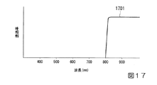
図17は、従来知られている蛍光内視鏡装置1Aの励起光カットフィルタ23の特性を示したグラフである。線1701は、励起光カットフィルタ23の透過率を示した線である。この特性により、励起光カットフィルタ23は、ICG蛍光物質の蛍光波長より長い波長の成分のみを透過し、赤外の撮像素子25が蛍光像のみを撮像できるようになっている。
FIG. 17 is a graph showing the characteristics of the excitation light cut filter 23 of the conventionally known fluorescence endoscope apparatus 1A. A
図18は、従来知られているICG蛍光物質の励起波長、蛍光波長の特性を示したグラフである。線1801は、励起光の強度を示した線である。線1802は、蛍光の強度を示した線である。ICG蛍光画像信号を生成するには、光源により被写体に照射された励起波長成分を除去して蛍光波長成分のみの光を撮像素子で撮像することが必要である。 FIG. 18 is a graph showing the excitation wavelength and fluorescence wavelength characteristics of a conventionally known ICG fluorescent material. A line 1801 is a line indicating the intensity of the excitation light. A line 1802 is a line indicating the intensity of fluorescence. In order to generate the ICG fluorescence image signal, it is necessary to remove the excitation wavelength component irradiated to the subject by the light source and to image only the light having the fluorescence wavelength component with the image sensor.
以上の構成により、蛍光内視鏡装置1Aは、ダイクロイックミラー22により可視と赤外を分離して、励起カットフィルタ23を透過することで可視像と蛍光像を同時に撮像することが可能である。なお、蛍光内視鏡装置1Aは、光源装置3Aから可視成分、レーザー光源7から励起光成分の光を被写体に照射して撮像出来るシステムになっている。
With the above configuration, the fluorescence endoscope apparatus 1 </ b> A can capture visible and fluorescent images simultaneously by separating visible and infrared by the dichroic mirror 22 and transmitting the excitation cut filter 23. . Note that the fluorescence endoscope apparatus 1A is a system that can irradiate a subject with light of a visible component from the
また、ハイブリッドPD−PDイメージャに関する技術が知られている(例えば、特許文献2参照)。図19は、従来知られている、撮像素子を2層積層し、上層を透過した光を用いて下層でも撮像を行うハイブリッド構造の撮像素子を示した断面図である。図19に示す例では、第1基板221と第2基板222とが積層されている。上層の第1基板221には、第1フォトダイオード223−1〜223−nが形成されている。下層の第2基板222には、第2フォトダイオード224−1〜224−nが形成されている。
A technique related to a hybrid PD-PD imager is known (see, for example, Patent Document 2). FIG. 19 is a cross-sectional view showing a conventionally known image pickup device having a hybrid structure in which two layers of image pickup devices are stacked and the lower layer is picked up using light transmitted through the upper layer. In the example shown in FIG. 19, a
この構成により、上層の第1基板221に形成された第1フォトダイオード223−1〜223−nを透過した光を、下層の第2基板222に形成された第2フォトダイオード224−1〜224−nで受光することができる。よって、第1基板221に形成された第1フォトダイオード223−1〜223−nと、第2基板222に形成された第2フォトダイオード224−1〜224−nとで同時に撮像することができる。
With this configuration, the light transmitted through the first photodiodes 223-1 to 223-n formed on the upper
CCD、CMOS撮像素子として広く使われている材料であるシリコンに入射する光は、波長が長いものほど深いところで吸収される。従って、図19のようなハイブリッドPD−PDイメージャで第1基板をBSIのように薄いイメージセンサにすると、図18のグラフに記載のICG蛍光波長のように長い波長の成分は第1基板221を透過して第2基板222で撮像できる。この場合、図14に記載の構成に比べてダイクロイックミラーが不要になり、カメラヘッドの小型化を可能にできる。
Light incident on silicon, which is a material widely used as a CCD or CMOS image sensor, is absorbed deeper as the wavelength increases. Accordingly, when the first substrate is made thin like BSI in the hybrid PD-PD imager as shown in FIG. 19, the long wavelength component such as the ICG fluorescence wavelength shown in the graph of FIG. The
しかしながら、従来知られている技術では次のような課題がある。図20は、従来知られているICG蛍光特性と積層撮像素子の特性を示したグラフである。線1081は、励起光の透過利率を示した線である。線1082は、蛍光の透過利率を示した線である。線1083は、第1基板221を透過する光の透過利率を示した線である。
However, conventionally known techniques have the following problems. FIG. 20 is a graph showing conventionally known ICG fluorescence characteristics and characteristics of a multilayer imaging device. A line 1081 is a line indicating the transmission rate of the excitation light. A line 1082 is a line indicating the transmission rate of fluorescence. A line 1083 is a line indicating a transmission rate of light transmitted through the
図20に示したグラフによれば、第1基板221を透過する光は、600〜800nmにおいて大きく減衰しているものの、無視できない量の光が下層に届いてしまっている。この600〜800nmの波長の光は、ICGの蛍光波長の検出を目的とする第2基板222での撮像には不要なものである。しかし、これを除去するために、第1基板221と第2基板222の層間に800nm以下の光をカットするカラーフィルタを配置する必要がある。しかしながら、第1基板221と第2基板222の層間に800nm以下の光をカットするカラーフィルタを配置することは、製造上の難しさがあるという問題がある。
According to the graph shown in FIG. 20, although the light transmitted through the
本発明は上記の問題を解決するためになされたものであり、ハイブリッド構造の撮像素子において、興味の波長に対応した蛍光画像を高精度に撮像することができる撮像素子および内視鏡装置を提供することを目的とする。 The present invention has been made to solve the above-described problems, and provides an imaging device and an endoscope apparatus capable of capturing a fluorescence image corresponding to a wavelength of interest with high accuracy in an imaging device having a hybrid structure. The purpose is to do.
本発明の一態様は、第1基板と、前記第1基板に積層された第2基板と、前記第1基板に行列状に配置され、第1受光素子を各々有し、可視帯域を含む第1波長帯域の入射光と前記第1波長帯域よりも波長が長い近赤外域を含む第2波長帯域の入射光とが照射され、前記第1波長帯域の光に応じた第1信号を生成する第1画素と、前記第2基板に行列状に配置され、前記第1画素を透過した光が照射される第2画素と、を備え、前記第2画素は、受光面と平行な第1PN接合面と、前記受光面と平行で前記第1PN接合面よりも深い位置に存在する第2PN接合面とを有し、前記第1PN接合面のP型層とN型層を同電位で接続し、前記第2PN接合面で得られた電荷から前記第2波長帯域の光に応じた第2信号を生成することを特徴とする撮像素子である。 In one embodiment of the present invention, a first substrate, a second substrate stacked on the first substrate, and a first light receiving element that are arranged in a matrix on the first substrate, each including a visible band, 1 wavelength than the first wavelength band and incident light wavelength band and the incident light of the second wavelength band including a long near-infrared region is irradiated, generating a first signal corresponding to light of said first wavelength band A first pixel and a second pixel arranged in a matrix on the second substrate and irradiated with light transmitted through the first pixel, the second pixel being a first PN junction parallel to the light receiving surface A second PN junction surface parallel to the light receiving surface and deeper than the first PN junction surface, and connecting the P-type layer and the N-type layer of the first PN junction surface at the same potential, and generates a second signal corresponding to light of the second wavelength band from the charge obtained in the previous SL first 2PN joint surface An image element.
また、本発明の他の態様の撮像素子において、前記第1PN接合面は、前記第1波長帯域の波長を含む光で電荷を生成することを特徴とする。 In the imaging device according to another aspect of the present invention, the first PN junction surface generates charges with light including a wavelength in the first wavelength band.
また、本発明の他の態様の撮像素子において、前記第1PN接合面で生成した第3信号を用いて前記第1信号を補正することを特徴とする。 In the imaging device according to another aspect of the present invention, the first signal is corrected using a third signal generated at the first PN junction surface.
また、本発明の他の態様の撮像素子において、前記第3信号を用いて、前記第1画素と前記第2画素とに入射する光の光量を制御することを特徴とする。 In the imaging device according to another aspect of the present invention, the amount of light incident on the first pixel and the second pixel is controlled using the third signal.
また、本発明の他の態様は、第1基板と、前記第1基板に積層された第2基板と、前記第1基板に行列状に配置され、第1受光素子を各々有し、可視帯域を含む第1波長帯域の入射光と前記第1波長帯域よりも波長が長い近赤外域を含む第2波長帯域の入射光とが照射され、前記第1波長帯域の光に応じた第1の信号を生成する第1画素と、前記第2基板に行列状に配置され、前記第1画素を透過した光が照射される第2画素と、を備え、前記第2画素は、受光面と平行な第1PN接合面と、前記受光面と平行で前記第1PN接合面よりも深い位置に存在する第2PN接合面とを有し、前記第1PN接合面のP型層とN型層を同電位で接続し、前記第2PN接合面で得られた電荷から前記第2波長帯域の光に応じた第2信号を生成し、前記第1画素は、受光面と平行な第3PN接合面と、前記受光面と平行で前記第3PN接合面よりも深い位置に存在する第4PN接合面とを有し、前記第3PN接合面のP型層とN型層を同電位で接続し、前記第4PN接合面で得られた電荷から前記第2波長帯域の光に応じた第4信号を生成することを特徴とする撮像素子である。 According to another aspect of the present invention, a first substrate, a second substrate stacked on the first substrate, and a first light receiving element arranged in a matrix on the first substrate, each having a visible band, wavelength than the first wavelength band and incident light in the first wavelength band and a second wavelength band of the incident light with long near-infrared region containing is irradiated, the first according to the light of the first wavelength band A first pixel that generates a signal; and a second pixel that is arranged in a matrix on the second substrate and is irradiated with light transmitted through the first pixel. The second pixel is parallel to a light receiving surface. A first PN junction surface and a second PN junction surface that is parallel to the light receiving surface and deeper than the first PN junction surface, and the P-type layer and the N-type layer of the first PN junction surface have the same potential. in connecting, to generate a second signal corresponding to light of the second wavelength band from the charge obtained by the first 2PN joint surface, said first Pixel includes a light receiving surface parallel to the 3PN joint surface, and a light receiving surface and the 4PN bonding surfaces existing at a position deeper than the first 3PN joint surface parallel, P-type layer of the first 3PN joint surface And the N-type layer are connected at the same potential, and a fourth signal corresponding to the light in the second wavelength band is generated from the charge obtained at the fourth PN junction surface.
また、本発明の他の態様は、インドシアニングリーン誘導体標識抗体からなる蛍光物質を被検査対象物に投与して内視鏡による診断を行う内視鏡装置において、撮像素子を備え、前記第1画素の受光面側に、可視帯域と蛍光物質の近赤外の蛍光波長帯域とを透過し、蛍光波長帯域と近接した励起波長帯域成分を透過しない光学フィルタが配置され、前記第1波長帯域は可視帯域を含み、前記第2波長帯域は蛍光物質の蛍光帯域を含むことを特徴とする内視鏡装置である。 According to another aspect of the present invention, there is provided an endoscope apparatus that performs diagnosis using an endoscope by administering a fluorescent substance composed of an indocyanine green derivative-labeled antibody to an object to be inspected. An optical filter that transmits the visible band and the near-infrared fluorescence wavelength band of the fluorescent material and does not transmit the excitation wavelength band component close to the fluorescence wavelength band is disposed on the light receiving surface side of the pixel, and the first wavelength band is An endoscope apparatus including a visible band, wherein the second wavelength band includes a fluorescent band of a fluorescent substance.
また、本発明の他の態様の内視鏡装置において、前記第1信号から可視帯域の第1画像が作成され、前記第2信号から蛍光波長帯域の第2画像が作成され、前記第1基板と、前記第2基板と、前記光学フィルタとは、内視鏡先端部に配置されることを特徴とする。 In the endoscope apparatus according to another aspect of the present invention, a first image in a visible band is created from the first signal, a second image in a fluorescence wavelength band is created from the second signal, and the first substrate The second substrate and the optical filter are arranged at the distal end portion of the endoscope.
本発明によれば、第1基板と、第1基板に積層された第2基板と、第1基板に行列状に配置され、第1受光素子を各々有し、可視帯域を含む第1波長帯域と第1波長帯域よりも波長が長い近赤外域を含む第2波長帯域の入射光が照射され、第1波長帯域の光に応じた第1信号を生成する第1画素と、第2基板に行列状に配置され、第1画素を透過した光が照射される第2画素と、を備える。また、第2画素は、受光面と平行な第1PN接合面と、受光面と平行で第1PN接合面よりも深い位置に存在する第2PN接合面とを有し、第2PN接合面で得られた電荷から第2波長帯域の光に応じた第2信号を生成する。従って、ハイブリッド構造の撮像素子において、興味の波長に対応した蛍光画像を高精度に撮像することができる。 According to the present invention, the first wavelength band including the first band, the second board laminated on the first board, and the first light receiving element arranged in a matrix on the first board, each including the first light receiving element. And a second pixel that is irradiated with incident light in a second wavelength band including a near-infrared band having a wavelength longer than the first wavelength band, and generates a first signal corresponding to the light in the first wavelength band; Second pixels arranged in a matrix and irradiated with light transmitted through the first pixels. The second pixel has a first PN junction surface parallel to the light receiving surface and a second PN junction surface that is parallel to the light receiving surface and exists at a position deeper than the first PN junction surface, and is obtained at the second PN junction surface. The second signal corresponding to the light in the second wavelength band is generated from the charged charges. Therefore, the fluorescence image corresponding to the wavelength of interest can be taken with high accuracy in the hybrid structure imaging device.
(第1の実施形態)
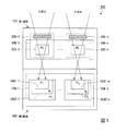
以下、本発明の第1の実施形態について図面を参照して説明する。初めに、撮像素子100の構成について説明する。図1は、本実施形態における撮像素子100の断面を示した断面図である。図示する例では、撮像素子100は、第1基板101と、第2基板102と、第1フォトダイオード103−1〜103−n(第1受光素子)と、第2画素104−1〜104−n(第2フォトダイオード、第2受光素子)と、カラーフィルタ105−1〜105−nとを備えている。また、入射光が照射される側を受光面とする。
(First embodiment)
Hereinafter, a first embodiment of the present invention will be described with reference to the drawings. First, the configuration of the
第1基板101と、第2基板102とは積層されている。第1基板101および第2基板102はシリコン基板である。また、第1基板101は入射された光のうち、一部の光を透過する。
The
第1フォトダイオード103−1〜103−nは、第1基板101内に配置されている。カラーフィルタ105−1〜105−nは、赤色の光を透過するフィルタ(R)、または、緑色の光を透過するフィルタ(G)、または、青色の光を透過するフィルタ(B)のいずれかであり、第1フォトダイオード103−1〜103−nの受光面側に配置されている。すなわち、第1フォトダイオード103−1〜103−n上にオンチップのRGBカラーフィルタ105−1〜105−nが配置されている。カラーフィルタ105−1〜105−nの配置については後述する。
The first photodiodes 103-1 to 103-n are arranged in the
なお、カラーフィルタ105−1〜105−nは、赤色の光を透過するフィルタ(R)であっても、緑色の光を透過するフィルタ(G)であっても、青色の光を透過するフィルタ(B)であっても、赤外波長の光も透過する。また、一般的には、デジタルカメラ用の撮像素子などでは受光面側にIRカットフィルタ(赤外光カットフィルタ)を設けるが、本実施形態ではIRカットフィルタを用いない。 Note that the color filters 105-1 to 105-n are filters that transmit blue light, whether they are filters (R) that transmit red light or filters (G) that transmit green light. Even in (B), light of infrared wavelength is transmitted. In general, an image sensor for a digital camera or the like is provided with an IR cut filter (infrared light cut filter) on the light receiving surface side, but the IR cut filter is not used in this embodiment.
本実施形態では、各第1フォトダイオード103−1〜103−nと、各カラーフィルタ105−1〜105−nとの組を第1画素106−1〜106−nとする。例えば、第1フォトダイオード103−1とカラーフィルタ105−1との組を第1画素106−1とする。第1フォトダイオード103−1〜103−nは、露光量に応じた第1信号を出力する。 In the present embodiment, a set of the first photodiodes 103-1 to 103-n and the color filters 105-1 to 105-n is referred to as first pixels 106-1 to 106-n. For example, a set of the first photodiode 103-1 and the color filter 105-1 is set as the first pixel 106-1. The first photodiodes 103-1 to 103-n output a first signal corresponding to the exposure amount.
第2画素104−1〜104−nは、第2基板102内に配置されている。また、第2画素104−1〜104−nは、P型層であるP11〜P1nと、N型層であるN1〜Nnと、P型層であるP21〜P2nとをそれぞれ含み、受光面と平行な第1PN接合面1041−1〜1041−nと、受光面と平行で第1PN接合面1041−1〜1041−nよりも深い位置に存在する第2PN接合面1042−1〜1042−nとを有する。この構成により、第2画素104−1〜104−nは、第2PN接合面1042−1〜1042−nで得られた電荷から第2信号を生成する。また、第2画素104−1〜104−nは、第1PN接合面1041−1〜1041−nで得られた電荷から第3信号を生成する。
The second pixels 104-1 to 104-n are disposed in the
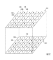
次に、カラーフィルタ105の配列について説明する。図2は、本実施形態におけるカラーフィルタ105の配列を示した概略図である。図2に示す例では、第1基板101には、6行6列の二次元状に規則的に配列された計36個の第1画素106が含まれている。また、第2基板102には、6行6列の二次元状に規則的に配列された計36個の第2画素104が含まれている。図2に示すとおり、第1基板101には、ベイヤ配列でカラーフィルタ105(カラーフィルタR、カラーフィルタG、カラーフィルタB)が配列されている。第2画素104には、第1画素106を透過した、赤外光を含む光が照射される。このような画素配置により、第1基板101では可視画像を、第2基板102では赤外画像を同時に撮像することが可能になる。
Next, the arrangement of the
なお、第1基板101に含まれる第1画素106と第2基板102に含まれる第2画素104との数および配列は、図2に示す例に限らず、どのような数および配列でもよい。また、図2に示す例では、第1画素106の下に第2画素104を対応して配置しているが、これに限らず、画素サイズを第1画素106に比べて第2画素104は整数倍にするなどの工夫も可能である。
Note that the number and arrangement of the
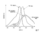
図3は、本実施形態において、励起光と、蛍光と、第1基板101を透過する光と、第1PN接合面1041−1〜1041−nが検出する光と、第2PN接合面1042−1〜1042−nが検出する光との特性を示したグラフである。グラフの横軸は波長(nm)を示す。グラフの縦軸は透過利率(%)を示す。線301は、励起光の特性を示した線である。線302は、蛍光の特性を示した線である。線303は、第1基板101を透過する光の特性を示した線である。線304は、第1PN接合面1041−1〜1041−nが検出する光の特性を示した線である。線305は、第2PN接合面1042−1〜1042−nが検出する光の特性を示した線である。
FIG. 3 shows the excitation light, the fluorescence, the light transmitted through the
本実施形態では、第2基板102に配置される第2画素104は、第1PN接合面1041−1〜1041−nと、第1PN接合面1041−1〜1041−nよりも深い位置に存在する第2PN接合面1042−1〜1042−nとを有する。この構成により、第2PN接合面1042−1〜1042−nは、第1基板101と、第1PN接合面1041−1〜1041−nとを透過した光(図3の領域306の光)を検出することができる。
In the present embodiment, the
これにより、第2PN接合面1042−1〜1042−nは、第1基板101や、浅い側の層に存在する第1PN接合面1041−1〜1041−nで不要な励起光成分(600〜800nmの波長の光)のより多くを除いた蛍光成分を検出し、第2波長帯域の光に応じた第2信号を生成することができる。従って、撮像素子100は、蛍光物質に照射した励起光成分や、可視成分を除去することができ、興味の波長(蛍光波長(860nm))の画像を高いS/Nで取得することができる。
Thereby, the second PN junction surfaces 1042-1 to 1042-n are unnecessary excitation light components (600 to 800 nm) in the first PN junction surfaces 1041-1 to 1041-n existing in the
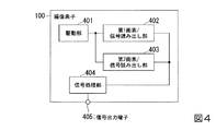
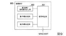
次に、撮像素子100の構成について説明する。図4は、本実施形態における撮像素子100の構成を示したブロック図である。撮像素子100は、駆動部401と、第1画素/信号読み出し部402と、第2画素/信号読み出し部403と、信号処理部404と、信号出力端子405とを備えている。駆動部401は、制御信号を送信し、第1画素/信号読み出し部402と、第2画素/信号読み出し部403とを駆動する。第1画素/信号読み出し部402は、第1画素106−1〜106−nを含み、第1画素106−1〜106−nが生成した第1信号を読み出し、信号処理部404に対して出力する。第2画素/信号読み出し部403は、第2画素104−1〜104を含み、第2画素104−1〜104−nが生成した第2信号を読み出し、信号処理部404に対して出力する。
Next, the configuration of the
信号処理部404は、第1画素/信号読み出し部402から入力された第1信号に基づいて、第1画像を生成する。第1信号は、赤色の光の強度に応じたR信号と、緑色の光の強度に応じたG信号と、青色の光の強度に応じたB信号である。すなわち、第1信号はRGB信号である。よって、信号処理部404が生成する第1画像は、RGB画像である。また、信号処理部404は、第2画素/信号読み出し部403から入力された第2信号に基づいて、第2画像を生成する。第2信号は、830nmを中心とする光の強度に応じた蛍光信号である。よって、信号処理部404が生成する第2画像は、蛍光画像である。また、信号処理部404は、生成した第1画像と第2画像とを信号出力端子405から出力する。なお、信号処理部404は、例えばノイズ低減や、RGB画像、蛍光画像の重畳などの画像処理を行うようにしてもよい。
The
次に、撮像素子100の駆動方法について説明する。図5は、本実施形態における撮像素子100の駆動タイミングを示したタイミングチャートである。図示する例では、第1画素106の駆動タイミングを示したタイミングチャート501と、第2画素104の駆動タイミングを示したタイミングチャート502とを示している。なお、タイミングチャートの横軸は時間である。
Next, a method for driving the
図示する通り、本実施形態では、第1画素106の電荷蓄積時間(露光時間)は、第2画素104の電荷蓄積時間(露光時間)よりも長い。これは、第2画素104には、第1画素106を透過した光のみが照射されるため、第2画素104に照射される光量が第1画素106に照射される光量よりも小さいためである。なお、本実施形態では、RGB画像と蛍光画像とのフレームレートが同一のフレームレートとなるように、各画素から信号を読み出す時間である読み出し時間を設定している。
As illustrated, in this embodiment, the charge accumulation time (exposure time) of the
上述したとおり、本実施形態によれば、第1基板101と第2基板102とを積層している。また、第2基板102は、第1基板101の受光面側から見て、第1基板101と重複する位置かつ第1基板101の受光面側とは反対側に配置されている。また、第1基板101は光を透過する。また、第1基板101を透過した光は、第2基板102に照射される。
As described above, according to this embodiment, the
これにより、第1基板101の第1画素106と、第2基板102の第2画素104とは同時に露光することができる。すなわち、第1画素106による第1信号の生成と、第2画素104による第2信号の生成とを同時に行うことができる。従って、信号処理部404は、第1信号に基づいた第1画像(RGB画像)と、第2信号に基づいた第2画像(蛍光画像)とを同時に生成することができる。
Thereby, the
また、本実施形態によれば、第2基板102に配置される第2画素104は、第1PN接合面1041−1〜1041−nと、第1PN接合面1041−1〜1041−nよりも深い位置に存在する第2PN接合面1042−1〜1042−nとを有する。この構成により、第2PN接合面1042−1〜1042−nは、第1基板101と、第1PN接合面1041−1〜1041−nとを透過した光を検出することができる。
Further, according to the present embodiment, the
これにより、第2PN接合面1042−1〜1042−nは、第1基板101や、浅い側の層に存在する第1PN接合面1041−1〜1041−nで不要な光の成分のより多くを除いた蛍光成分を検出し、第2波長帯域の光に応じた第2信号を生成することができる。従って、撮像素子100は、蛍光物質に照射した励起光成分や、可視成分を除去することができ、興味の波長に対応した蛍光画像を高精度に撮像することができる。
As a result, the second PN junction surfaces 1042-1 to 1042-n cause the
(第2の実施形態)
次に、本発明の第2の実施形態について説明する。第1の実施形態における撮像素子100と本実施形態における撮像素子とで異なる点は、第1基板が有する第1フォトダイオードの構成である。なお、その他の構成は、第1の実施形態と同様である。
(Second Embodiment)
Next, a second embodiment of the present invention will be described. The difference between the
図6は、本実施形態における撮像素子600の断面を示した断面図である。図示する例では、撮像素子600は、第1基板601と、第2基板102と、第1フォトダイオード603−1〜603−n(第1受光素子)と、第2画素104−1〜104−n(第2フォトダイオード、第2受光素子)と、カラーフィルタ105−1〜105−nとを備えている。また、入射光が照射される側を受光面とする。
FIG. 6 is a cross-sectional view showing a cross section of the
第1基板601と、第2基板102とは積層されている。第1基板601および第2基板102はシリコン基板である。また、第1基板601は入射された光のうち、一部の光を透過する。
The first substrate 601 and the
第1フォトダイオード603−1〜603−nは、第1基板601内に配置されている。また、第1フォトダイオード603−1〜603−nは、P型層である1P11〜1P1nと、N型層である1N1〜1Nnと、P型層である1P21〜1P2nとをそれぞれ含み、受光面と平行な第1PN接合面6031−1〜6031−nと、受光面と平行で第1PN接合面6031−1〜6031−nよりも深い位置に存在する第2PN接合面6032−1〜6032−nとを有する。この構成により、第1フォトダイオード603−1〜603−nは、第2PN接合面6032−1〜6032−nで得られた電荷から第2信号を生成する。また、第1フォトダイオード603−1〜603−nは、第1PN接合面6031−1〜6031−nで得られた電荷から第1信号を生成する。
The first photodiodes 603-1 to 603-n are arranged in the first substrate 601. The first photodiodes 603-1 to 603-n include P-type layers 1P1 1 to 1P1 n , N-type layers 1N 1 to 1N n , and P-type layers 1P2 1 to 1P2 n . First PN junction surfaces 6031-1 to 6031-n that are parallel to the light receiving surface, and second
カラーフィルタ105−1〜105−nは、赤色の光を透過するフィルタ(R)、または、緑色の光を透過するフィルタ(G)、または、青色の光を透過するフィルタ(B)のいずれかであり、第1フォトダイオード603−1〜603−nの受光面側に配置されている。すなわち、第1フォトダイオード603−1〜603−n上にオンチップのRGBカラーフィルタ105−1〜105−nが配置されている。カラーフィルタ105−1〜105−nの配置は、第1の実施形態と同様である。 The color filters 105-1 to 105-n are either a filter (R) that transmits red light, a filter (G) that transmits green light, or a filter (B) that transmits blue light. And arranged on the light receiving surface side of the first photodiodes 603-1 to 603-n. That is, on-chip RGB color filters 105-1 to 105-n are arranged on the first photodiodes 603-1 to 603-n. The arrangement of the color filters 105-1 to 105-n is the same as that in the first embodiment.
本実施形態では、各第1フォトダイオード603−1〜603−nと、各カラーフィルタ105−1〜105−nとの組を第1画素606−1〜606−nとする。例えば、第1フォトダイオード603−1とカラーフィルタ105−1との組を第1画素606−1とする。 In the present embodiment, a set of the first photodiodes 603-1 to 603-n and the color filters 105-1 to 105-n is referred to as first pixels 606-1 to 606-n. For example, a set of the first photodiode 603-1 and the color filter 105-1 is a first pixel 606-1.
第2画素104−1〜104−nは、第2基板102内に配置されている。また、第2画素104−1〜104−nは、P型層であるP11〜P1nと、N型層であるN1〜Nnと、P型層であるP21〜P2nとをそれぞれ含み、受光面と平行な第1PN接合面1041−1〜1041−nと、受光面と平行で第1PN接合面1041−1〜1041−nよりも深い位置に存在する第2PN接合面1042−1〜1042−nとを有する。この構成により、第2画素104−1〜104−nは、第2PN接合面1042−1〜1042−nで得られた電荷から第2信号を生成する。また、第2画素104−1〜104−nは、第1PN接合面1041−1〜1041−nで得られた電荷から第3信号を生成する。
The second pixels 104-1 to 104-n are disposed in the
図7は、本実施形態において、励起光と、蛍光と、第1基板101を透過する光と、第2PN接合面1042−1〜1042−nが検出する光との特性を示したグラフである。グラフの横軸は波長(nm)を示す。グラフの縦軸は透過利率(%)を示す。線701は、励起光の特性を示した線である。線702は、蛍光の特性を示した線である。線703は、第1基板601を透過する光の特性を示した線である。線704は、第2PN接合面1042−1〜1042−nが検出する光の特性を示した線である。
FIG. 7 is a graph illustrating characteristics of excitation light, fluorescence, light transmitted through the
本実施形態では、第1フォトダイオード603−1〜603−nは、P型層である1P11〜1P1nと、N型層である1N1〜1Nnと、P型層である1P21〜1P2nとをそれぞれ含み、受光面と平行な第1PN接合面6031−1〜6031−nと、受光面と平行で第1PN接合面6031−1〜6031−nよりも深い位置に存在する第2PN接合面6032−1〜6032−nとを有する。この構成により、第1基板601を透過する励起光成分が第1の実施形態(図3の線303参照)よりも少なくなる。 In the present embodiment, the first photodiodes 603-1 to 603-n are 1P1 1 to 1P1 n that are P-type layers, 1N 1 to 1N n that are N-type layers, and 1P2 1 to 1P that are P-type layers. wherein 1P2 n and, respectively, the light-receiving surface parallel to the 1PN joint surface 6031-1~6031-n, the 2PN present in a position deeper than the 1PN joint surface 6031-1~6031-n in parallel to the receiving surface The bonding surfaces 6032-1 to 6032-n are included. With this configuration, the excitation light component transmitted through the first substrate 601 is less than that in the first embodiment (see the line 303 in FIG. 3).
これにより、第2PN接合面1042−1〜1042−nは、第1基板601や、浅い側の層に存在する第1PN接合面1041−1〜1041−nで不要な光の成分を除いた蛍光成分を検出し、第2波長帯域の光に応じた第2信号を生成することができる。従って、撮像素子600は、蛍光物質に照射した励起光成分や、可視成分を除去することができ、興味の波長に対応した蛍光画像を高精度に撮像することができる。
As a result, the second PN junction surfaces 1042-1 to 1042-n are fluorescent light from which unnecessary light components are removed from the first PN junction surfaces 1041-1 to 1041-n existing in the first substrate 601 or the shallower layer. The component can be detected, and a second signal corresponding to the light in the second wavelength band can be generated. Therefore, the
(第3の実施形態)
次に、本発明の第3の実施形態について説明する。第1の実施形態における撮像素子100と本実施形態における撮像素子とで異なる点は、第2画素が含んでいる第1PN接合面のP型層とN型層とを電気的に接続し、同電位とする点である。なお、その他の構成は、第1の実施形態と同様である。
(Third embodiment)
Next, a third embodiment of the present invention will be described. The difference between the
図8は、本実施形態における撮像素子800の断面を示した断面図である。図示する例では、撮像素子800は、第1基板101と、第2基板802と、第1フォトダイオード103−1〜103−n(第1受光素子)と、第2画素804−1〜804−n(第2フォトダイオード、第2受光素子)と、カラーフィルタ105−1〜105−nとを備えている。また、入射光が照射される側を受光面とする。
FIG. 8 is a cross-sectional view showing a cross section of the
第1基板101と、第2基板802とは積層されている。第1基板101および第2基板802はシリコン基板である。また、第1基板101は入射された光のうち、一部の光を透過する。
The
第1フォトダイオード103−1〜103−nは、第1基板101内に配置されている。カラーフィルタ105−1〜105−nは、赤色の光を透過するフィルタ(R)、または、緑色の光を透過するフィルタ(G)、または、青色の光を透過するフィルタ(B)のいずれかであり、第1フォトダイオード103−1〜103−nの受光面側に配置されている。すなわち、第1フォトダイオード103−1〜103−n上にオンチップのRGBカラーフィルタ105−1〜105−nが配置されている。カラーフィルタ105−1〜105−nの配置は、第1の実施形態と同様である。
The first photodiodes 103-1 to 103-n are arranged in the
本実施形態では、各第1フォトダイオード103−1〜103−nと、各カラーフィルタ105−1〜105−nとの組を第1画素106−1〜106−nとする。例えば、第1フォトダイオード103−1とカラーフィルタ105−1との組を第1画素106−1とする。第1フォトダイオード103−1〜103−nは、露光量に応じた第1信号を出力する。 In the present embodiment, a set of the first photodiodes 103-1 to 103-n and the color filters 105-1 to 105-n is referred to as first pixels 106-1 to 106-n. For example, a set of the first photodiode 103-1 and the color filter 105-1 is set as the first pixel 106-1. The first photodiodes 103-1 to 103-n output a first signal corresponding to the exposure amount.
第2画素804−1〜804−nは、第2基板802内に配置されている。また、第2画素804−1〜804−nは、P型層であるP11〜P1nと、N型層であるN1〜Nnと、P型層であるP21〜P2nとをそれぞれ含み、受光面と平行な第1PN接合面8041−1〜8041−nと、受光面と平行で第1PN接合面8041−1〜8041−nよりも深い位置に存在する第2PN接合面8042−1〜8042−nとを有する。また、第1PN接合面8041のP型層P11〜P1nとN型層N1〜Nnとを、それぞれ接続部8043−1〜8043−nを用いて電気的に接続し、同電位としている。これにより、第1PN接合面8041による電荷の発生を抑制することができる。従って、第2PN接合面8042−1〜8042−nが生成する第2信号の精度をより向上させることができる。
The second pixels 804-1 to 804-n are arranged in the second substrate 802. The second pixel 804-1~804-n includes a P1 1 to P1 n is a P-type layer, and N 1 to N n is a N-type layer, a P2 1 to P2 n is a P-type layer Each of the first PN junction surfaces 8041-1 to 8041-n parallel to the light receiving surface, and the second PN junction surface 8042- parallel to the light receiving surface and deeper than the first PN junction surfaces 8041-1 to 8041-n. 1-8042-n. Further, the P-type layers P1 1 to P1 n and the N-type layers N 1 to N n of the first
(第4の実施形態)
次に、本発明の第4の実施形態について説明する。第1の実施形態における撮像素子100と本実施形態における撮像素子とで異なる点は、第1PN接合面1041−1〜1041−nで生成した第3信号と、第2PN接合面1042−1〜1042−nで生成した信号とを用いて、第1基板101の第1画素106−1〜106−nで生成した第1信号によるRGB画像を補正する点である。なお、その他の構成は、第1の実施形態と同様である。
(Fourth embodiment)
Next, a fourth embodiment of the present invention will be described. The difference between the
図9は、本実施形態における撮像素子900の構成を示したブロック図である。撮像素子900は、第1画素/信号読み出し部402と、信号補正部901とを備えている。第1画素106−1〜106−nが生成した第1信号は、可視成分(RGB成分)以外に赤外成分を含んでいる。また、第1PN接合面1041−1〜1041−nが生成した第3信号と、第2PN接合面1042−1〜1042−nが生成した信号は、第1信号が含んでいる赤外成分に相当する信号である。よって、信号補正部901は、第1信号から赤外成分を差分処理することで、可視成分のみで画像を生成することができる。従って、第1画像(RGB画像、可視画像)の画質をより向上させることができる。
FIG. 9 is a block diagram illustrating a configuration of the
(第5の実施形態)
次に、本発明の第5の実施形態について説明する。本実施形態と第1の実施形態とで異なる点は、撮像素子の受光面側にICGフィルタを備える点である。なお、その他の構成は、第1の実施形態と同様である。
(Fifth embodiment)
Next, a fifth embodiment of the present invention will be described. The difference between the present embodiment and the first embodiment is that an ICG filter is provided on the light receiving surface side of the image sensor. Other configurations are the same as those in the first embodiment.
図10は、本実施形態における撮像素子1200の構成を示した概略図である。図10に示す撮像素子1200は、第1基板101と、第2基板102と、複数の第1フォトダイオード103(第1受光素子)と、複数の第2画素104(第2フォトダイオード、第2受光素子)と、複数のカラーフィルタ105と、ICGフィルタ1201とを備えている。
FIG. 10 is a schematic diagram illustrating the configuration of the
第1基板101と、第2基板102と、第1フォトダイオード103と、第2画素104と、カラーフィルタ105との構成は第1の実施形態と同様である。ICGフィルタ1201は、カラーフィルタ105の受光面側に配置されている。ICGフィルタ1201は、ICGの励起光をカットして蛍光波長のみを透過する光学フィルタである。
The configurations of the
図11は、本実施形態において、ICGフィルタ1201の分光特性を示したグラフである。グラフの横軸は波長(nm)を示す。グラフの縦軸は透過率を示す。線1301は、ICGフィルタ1201の可視領域の透過率を示す。線1302は、ICGフィルタ1201の蛍光の透過率を示す。図11に示すように、ICGフィルタ1201は、可視領域の光と蛍光とを透過し、励起光を透過しない。なお、図11に示す例では、蛍光部分を900nmで減衰するICGフィルタ1201を示しているが、800nm以上を全て透過するハイパスタイプであってもよい。
FIG. 11 is a graph showing the spectral characteristics of the
これにより、第2PN接合面1042−1〜1042−nは、ICGフィルタ1201と、第1基板101と、浅い側の層に存在する第1PN接合面1041−1〜1041−nで不要な光の成分を除いた蛍光成分を検出し、第2波長帯域の光に応じた第2信号を生成することができる。従って、撮像素子1200は、蛍光物質に照射した励起光成分や、可視成分を除去することができ、興味の波長に対応した蛍光画像を高精度に撮像することができる。
As a result, the second PN junction surfaces 1042-1 to 1042-n cause unnecessary light to pass through the
(第6の実施形態)
次に、本発明の第6の実施形態について説明する。本実施形態では、第1の実施形態〜第5の実施形態に記載した撮像素子のうち、いずれかを内蔵した内視鏡装置について説明する。
(Sixth embodiment)
Next, a sixth embodiment of the present invention will be described. In the present embodiment, an endoscope apparatus incorporating any one of the imaging elements described in the first to fifth embodiments will be described.
図12は、本実施形態における内視鏡装置の構成を示したブロック図である。図示する例では、内視鏡装置1000は、内視鏡スコープ1001と、演算部1002と、モニタ1003と、光源部1004とを備えている。演算部1002は、内視鏡装置1000の各部の制御を行う。モニタ1003は、例えば液晶ディスプレイであり、画像を表示する。光源部1004は、例えはLEDであり、光を発する。
FIG. 12 is a block diagram illustrating a configuration of the endoscope apparatus according to the present embodiment. In the illustrated example, the
内視鏡スコープ1001は、撮像素子1011と、撮像レンズ1012と、ライトガイド1013と、照明レンズ1014とを備えている。撮像素子1011は、第1の実施形態〜第4の実施形態に記載した撮像素子のいずれかである。撮像素子1011は、内視鏡スコープ1001の先端部に配置されている。また、撮像レンズ1012は、撮像素子1011の受光面側に配置されている。また、照明レンズ1014は、内視鏡スコープ1001の先端部に配置されている。 The endoscope scope 1001 includes an imaging element 1011, an imaging lens 1012, a light guide 1013, and an illumination lens 1014. The image sensor 1011 is one of the image sensors described in the first to fourth embodiments. The image sensor 1011 is disposed at the distal end portion of the endoscope scope 1001. The imaging lens 1012 is disposed on the light receiving surface side of the imaging element 1011. The illumination lens 1014 is disposed at the distal end portion of the endoscope scope 1001.
ライトガイド1013は、光源部1004が発した光を照明レンズ1014に照射する。照明レンズ1014は、ライトガイド1013から照射される光を集光し、被写体に照射する。撮像レンズ1012は、被写体からの光を集光し、撮像素子1011に照射する。撮像素子1011は、撮像レンズ1012により照射された光に基づいて、第1画像と第2画像とを生成する。演算部1002は、撮像素子1011が生成した第1画像と第2画像とを、モニタ1003に表示させる。
The light guide 1013 irradiates the illumination lens 1014 with light emitted from the
例えば、第1の実施形態〜第5の実施形態に記載した撮像素子は、小型化にしつつ、高精度なRGB画像と蛍光画像とを同時に撮像することができる。よって、第1の実施形態〜第5の実施形態に記載した撮像素子のいずれかを内視鏡装置1000に用いることで、高精度なRGB画像と蛍光画像とを同時に撮像することができる。例えば、高精度なRGB画像と蛍光画像とを、がん診断や外科手術時のICG観察に役立てることができる。
For example, the imaging elements described in the first to fifth embodiments can simultaneously capture a highly accurate RGB image and fluorescent image while reducing the size. Therefore, by using any of the imaging elements described in the first to fifth embodiments for the
(第7の実施形態)
次に、本発明の第7の実施形態について説明する。本実施形態と第6の実施形態とで異なる点は、第1PN接合面1041−1〜1041−nが生成した第3信号を用いて、光源部1004の光量(励起光成分)を調整する点である。なお、その他の構成は、第6の実施形態と同様である。
(Seventh embodiment)
Next, a seventh embodiment of the present invention will be described. The difference between this embodiment and the sixth embodiment is that the amount of light (excitation light component) of the
図13は、本実施形態における撮像素子1100の構成を示したブロック図である。撮像素子1100は、光量調整部1101を備えている。第1PN接合面1041−1〜1041−nが生成した第3信号は、励起光量に応じた信号である。例えば、ICG蛍光物質では励起波長も赤外のため観察者が目視で光量調整することは出来ない。そこで、本実施形態では、光量調整部1101は、第1PN接合面1041−1〜1041−nが生成した第3信号に基づいて光源部1004の光量(励起光成分)を調整する。これにより、ICG蛍光物質を投与した被写体に照射する光量を最適化することができるため、蛍光画像の画質をさらに向上させることができる。
FIG. 13 is a block diagram illustrating a configuration of the image sensor 1100 according to the present embodiment. The image sensor 1100 includes a light
以上、この発明の第1の実施形態〜第7の実施形態について図面を参照して詳述してきたが、具体的な構成はこの実施形態に限られるものではなく、この発明の要旨を逸脱しない範囲の設計等も含まれる。例えば、各実施形態で示した構成を組み合わせてもよい。 Although the first to seventh embodiments of the present invention have been described in detail with reference to the drawings, the specific configuration is not limited to this embodiment and does not depart from the gist of the present invention. Range design etc. are also included. For example, you may combine the structure shown by each embodiment.
100,600,800,900,1011,1100,1200・・・撮像素子、101,221,601・・・第1基板、102,222,802・・・第2基板、103−1〜103−n,223−1〜223−n,603−1〜603−n・・・第1フォトダイオード、104−1〜104,224−1〜224−n,804−1〜804−n・・・第2画素、105−1〜105−n・・・カラーフィルタ、106−1〜106−n,606−1〜606−n・・・第1画素、401・・・駆動部、402・・・第1画素/信号読み出し部、403・・・第2画素/信号読み出し部、404・・・信号処理部、405・・・信号出力端子、901・・・信号補正部、1000・・・内視鏡装置、1001・・・内視鏡スコープ、1002・・・演算部、1003・・・モニタ、1004・・・光源部、1012・・・撮像レンズ、1013・・・ライトガイド、1014・・・照明レンズ、1041−1〜1041−n,6031−1〜6031−n,8041−1〜8041−n・・・第1PN接合面、1042−1〜1042−n,6032−1〜6032−n,8042−1〜8042−n・・・第2PN接合面、1101・・・光量調整部、1201・・・ICGフィルタ、8043−1〜8043−n・・・接続部
100, 600, 800, 900, 1011, 1100, 1200...
Claims (7)
前記第1基板に積層された第2基板と、
前記第1基板に行列状に配置され、第1受光素子を各々有し、可視帯域を含む第1波長帯域の入射光と前記第1波長帯域よりも波長が長い近赤外域を含む第2波長帯域の入射光とが照射され、前記第1波長帯域の光に応じた第1信号を生成する第1画素と、
前記第2基板に行列状に配置され、前記第1画素を透過した光が照射される第2画素と、
を備え、
前記第2画素は、受光面と平行な第1PN接合面と、前記受光面と平行で前記第1PN接合面よりも深い位置に存在する第2PN接合面とを有し、前記第1PN接合面のP型層とN型層を同電位で接続し、前記第2PN接合面で得られた電荷から前記第2波長帯域の光に応じた第2信号を生成する
ことを特徴とする撮像素子。 A first substrate;
A second substrate stacked on the first substrate;
A second wavelength that is arranged in a matrix on the first substrate, includes first light receiving elements, and includes a first wavelength band including a visible band and a near-infrared band having a wavelength longer than the first wavelength band. A first pixel that is irradiated with incident light in a band and generates a first signal according to the light in the first wavelength band;
Second pixels arranged in a matrix on the second substrate and irradiated with light transmitted through the first pixels;
With
The second pixel includes a first PN junction surface parallel to the light receiving surface and a second PN junction surface parallel to the light receiving surface and present at a position deeper than the first PN junction surface. An image sensor, wherein a P-type layer and an N-type layer are connected at the same potential, and a second signal corresponding to light in the second wavelength band is generated from an electric charge obtained at the second PN junction surface.
ことを特徴とする請求項1に記載の撮像素子。 Wherein said 1PN bonding surface, the imaging device according to claim 1, characterized in that to generate an electric charge by light including a wavelength of said first wavelength band.
ことを特徴とする請求項1または請求項2に記載の撮像素子。 Imaging device according to claim 1 or claim 2, characterized in that to correct the first signal using a third signal generated by the first 1PN joint surface.
ことを特徴とする請求項3に記載の撮像素子。 The third signal using an imaging device according to claim 3, characterized in that to control the amount of light incident on the first pixel and the second pixel.
前記第1基板に積層された第2基板と、
前記第1基板に行列状に配置され、第1受光素子を各々有し、可視帯域を含む第1波長帯域の入射光と前記第1波長帯域よりも波長が長い近赤外域を含む第2波長帯域の入射光とが照射され、前記第1波長帯域の光に応じた第1の信号を生成する第1画素と、
前記第2基板に行列状に配置され、前記第1画素を透過した光が照射される第2画素と、
を備え、
前記第2画素は、受光面と平行な第1PN接合面と、前記受光面と平行で前記第1PN接合面よりも深い位置に存在する第2PN接合面とを有し、前記第1PN接合面のP型層とN型層を同電位で接続し、前記第2PN接合面で得られた電荷から前記第2波長帯域の光に応じた第2信号を生成し、
前記第1画素は、受光面と平行な第3PN接合面と、前記受光面と平行で前記第3PN接合面よりも深い位置に存在する第4PN接合面とを有し、前記第3PN接合面のP型層とN型層を同電位で接続し、前記第4PN接合面で得られた電荷から前記第2波長帯域の光に応じた第4信号を生成する
ことを特徴とする撮像素子。 A first substrate;
A second substrate stacked on the first substrate;
A second wavelength that is arranged in a matrix on the first substrate, includes first light receiving elements, and includes a first wavelength band including a visible band and a near-infrared band having a wavelength longer than the first wavelength band. A first pixel that is irradiated with incident light in a band and generates a first signal according to the light in the first wavelength band;
Second pixels arranged in a matrix on the second substrate and irradiated with light transmitted through the first pixels;
With
The second pixel includes a first PN junction surface parallel to the light receiving surface and a second PN junction surface parallel to the light receiving surface and present at a position deeper than the first PN junction surface. Connecting the P-type layer and the N-type layer at the same potential, and generating a second signal corresponding to the light in the second wavelength band from the charge obtained at the second PN junction surface;
The first pixel has a third PN junction surface parallel to the light receiving surface, and a fourth PN junction surface parallel to the light receiving surface and present at a position deeper than the third PN junction surface. An image sensor, wherein a P-type layer and an N-type layer are connected at the same potential, and a fourth signal corresponding to light in the second wavelength band is generated from the charge obtained at the fourth PN junction surface.
請求項1から請求項5のいずれか1項に記載の撮像素子
を備え、
前記第1画素の受光面側に、可視帯域と蛍光物質の近赤外の蛍光波長帯域とを透過し、蛍光波長帯域と近接した励起波長帯域成分を透過しない光学フィルタが配置され、
前記第1波長帯域は可視帯域を含み、前記第2波長帯域は蛍光物質の蛍光帯域を含む
ことを特徴とする内視鏡装置。 In an endoscopic device for performing an endoscopic diagnosis by administering a fluorescent substance composed of an indocyanine green derivative-labeled antibody to a test object
The image pickup device according to any one of claims 1 to 5 , comprising:
An optical filter that transmits the visible band and the near-infrared fluorescence wavelength band of the fluorescent material and does not transmit the excitation wavelength band component close to the fluorescence wavelength band is disposed on the light receiving surface side of the first pixel,
The first wavelength band includes a visible band, and the second wavelength band includes a fluorescent band of a fluorescent material.
前記第2信号から蛍光波長帯域の第2画像が作成され、
前記第1基板と、前記第2基板と、前記光学フィルタとは、内視鏡先端部に配置される
ことを特徴とする、請求項5を引用しない請求項6に記載の内視鏡装置。 A first image in the visible band is created from the first signal,
A second image of the fluorescence wavelength band is created from the second signal,
Wherein a first substrate, a second substrate, and the optical filter is characterized in that arranged in the endoscope tip portion, the endoscope apparatus according to claim 6 which does not quote the claim 5.
Priority Applications (5)
| Application Number | Priority Date | Filing Date | Title |
|---|---|---|---|
| JP2014183211A JP6469996B2 (en) | 2014-09-09 | 2014-09-09 | Imaging device and endoscope apparatus |
| PCT/JP2015/075487 WO2016039345A1 (en) | 2014-09-09 | 2015-09-08 | Image pickup element and endoscope device |
| CN201580047380.7A CN107079136B (en) | 2014-09-09 | 2015-09-08 | Photographing element and endoscope apparatus |
| DE112015003666.0T DE112015003666T5 (en) | 2014-09-09 | 2015-09-08 | Image pickup element and endoscope device |
| US15/450,520 US10335019B2 (en) | 2014-09-09 | 2017-03-06 | Image pickup element and endoscope device |
Applications Claiming Priority (1)
| Application Number | Priority Date | Filing Date | Title |
|---|---|---|---|
| JP2014183211A JP6469996B2 (en) | 2014-09-09 | 2014-09-09 | Imaging device and endoscope apparatus |
Publications (3)
| Publication Number | Publication Date |
|---|---|
| JP2016058866A JP2016058866A (en) | 2016-04-21 |
| JP2016058866A5 JP2016058866A5 (en) | 2017-10-19 |
| JP6469996B2 true JP6469996B2 (en) | 2019-02-13 |
Family
ID=55459089
Family Applications (1)
| Application Number | Title | Priority Date | Filing Date |
|---|---|---|---|
| JP2014183211A Expired - Fee Related JP6469996B2 (en) | 2014-09-09 | 2014-09-09 | Imaging device and endoscope apparatus |
Country Status (5)
| Country | Link |
|---|---|
| US (1) | US10335019B2 (en) |
| JP (1) | JP6469996B2 (en) |
| CN (1) | CN107079136B (en) |
| DE (1) | DE112015003666T5 (en) |
| WO (1) | WO2016039345A1 (en) |
Families Citing this family (11)
| Publication number | Priority date | Publication date | Assignee | Title |
|---|---|---|---|---|
| JP6660824B2 (en) * | 2016-06-24 | 2020-03-11 | 富士フイルム株式会社 | Endoscope device |
| JP6660823B2 (en) * | 2016-06-24 | 2020-03-11 | 富士フイルム株式会社 | Endoscope device |
| JP7140469B2 (en) * | 2016-07-15 | 2022-09-21 | キヤノン株式会社 | Photoelectric conversion device and imaging system |
| JP6746476B2 (en) * | 2016-11-24 | 2020-08-26 | キヤノン株式会社 | Imaging device, imaging system, and moving body |
| WO2018225122A1 (en) * | 2017-06-05 | 2018-12-13 | オリンパス株式会社 | Endoscope device |
| JP6920110B2 (en) * | 2017-06-13 | 2021-08-18 | ルネサスエレクトロニクス株式会社 | Solid-state image sensor and its manufacturing method |
| CN108881533B (en) * | 2018-06-06 | 2020-09-11 | 北京小米移动软件有限公司 | Terminal device |
| CN113164054A (en) * | 2018-11-30 | 2021-07-23 | 直观外科手术操作公司 | Medical imaging system and method |
| CN111272715B (en) * | 2018-12-04 | 2023-03-14 | 长春长光华大智造测序设备有限公司 | Fluorescence imaging system of gene sequencer |
| JP2022026845A (en) * | 2020-07-31 | 2022-02-10 | 浜松ホトニクス株式会社 | Imaging apparatus |
| JP2022049487A (en) * | 2020-09-16 | 2022-03-29 | ソニーグループ株式会社 | Solid-state imaging device and electronic apparatus |
Family Cites Families (17)
| Publication number | Priority date | Publication date | Assignee | Title |
|---|---|---|---|---|
| JP3962122B2 (en) | 1996-11-20 | 2007-08-22 | オリンパス株式会社 | Endoscope device |
| JP3938675B2 (en) * | 2001-10-26 | 2007-06-27 | オリンパス株式会社 | Light source device |
| JP4817584B2 (en) * | 2002-05-08 | 2011-11-16 | キヤノン株式会社 | Color image sensor |
| US7129466B2 (en) | 2002-05-08 | 2006-10-31 | Canon Kabushiki Kaisha | Color image pickup device and color light-receiving device |
| JP4507769B2 (en) * | 2004-08-31 | 2010-07-21 | ソニー株式会社 | Solid-state image sensor, camera module, and electronic device module |
| JP4984634B2 (en) * | 2005-07-21 | 2012-07-25 | ソニー株式会社 | Physical information acquisition method and physical information acquisition device |
| US8111286B2 (en) * | 2006-09-28 | 2012-02-07 | Fujifilm Corporation | Image processing apparatus, endoscope, and computer readable medium |
| JP5191327B2 (en) * | 2008-09-17 | 2013-05-08 | 富士フイルム株式会社 | Image acquisition device and method of operating image acquisition device |
| JP4772843B2 (en) * | 2008-09-17 | 2011-09-14 | シャープ株式会社 | Semiconductor device and manufacturing method thereof |
| US8203709B2 (en) | 2008-09-17 | 2012-06-19 | Fujifilm Corporation | Image obtaining method and image obtaining apparatus |
| KR20120114895A (en) * | 2011-04-08 | 2012-10-17 | 삼성전자주식회사 | Endoscope apparatus and image acquisition method of the endoscope |
| JP2013070030A (en) * | 2011-09-06 | 2013-04-18 | Sony Corp | Imaging device, electronic apparatus, and information processor |
| US20130075607A1 (en) * | 2011-09-22 | 2013-03-28 | Manoj Bikumandla | Image sensors having stacked photodetector arrays |
| US9057228B2 (en) * | 2012-06-29 | 2015-06-16 | Baker Hughes Incorporated | Wellbore tools with non-hydrocarbon-based greases and methods of making such wellbore tools |
| RU2630261C2 (en) * | 2012-07-12 | 2017-09-06 | Сони Корпорейшн | Transmission apparatus, data processing technique, programme, receiving apparatus and app interaction system |
| DE102012213467B4 (en) * | 2012-07-31 | 2023-12-07 | Coretronic Corporation | DEVICE FOR PROVIDING ELECTROMAGNETIC RADIATION |
| JP6076093B2 (en) | 2013-01-08 | 2017-02-08 | オリンパス株式会社 | Imaging device |
-
2014
- 2014-09-09 JP JP2014183211A patent/JP6469996B2/en not_active Expired - Fee Related
-
2015
- 2015-09-08 DE DE112015003666.0T patent/DE112015003666T5/en not_active Withdrawn
- 2015-09-08 WO PCT/JP2015/075487 patent/WO2016039345A1/en active Application Filing
- 2015-09-08 CN CN201580047380.7A patent/CN107079136B/en active Active
-
2017
- 2017-03-06 US US15/450,520 patent/US10335019B2/en not_active Expired - Fee Related
Also Published As
| Publication number | Publication date |
|---|---|
| DE112015003666T5 (en) | 2017-05-18 |
| US20170172393A1 (en) | 2017-06-22 |
| WO2016039345A1 (en) | 2016-03-17 |
| CN107079136B (en) | 2019-06-21 |
| US10335019B2 (en) | 2019-07-02 |
| CN107079136A (en) | 2017-08-18 |
| JP2016058866A (en) | 2016-04-21 |
Similar Documents
| Publication | Publication Date | Title |
|---|---|---|
| JP6469996B2 (en) | Imaging device and endoscope apparatus | |
| US11419501B2 (en) | Fluorescence observation device and fluorescence observation endoscope device | |
| JP7314976B2 (en) | Imaging device and imaging method | |
| JP6076093B2 (en) | Imaging device | |
| JP5507376B2 (en) | Imaging device | |
| US10602919B2 (en) | Imaging device | |
| JP6027832B2 (en) | Imaging device | |
| US10874293B2 (en) | Endoscope device | |
| WO2016129062A1 (en) | Image processing device, endoscope system, imaging device, image processing method, and program | |
| WO2016056157A1 (en) | Color separation prism and imaging device | |
| JP2016058866A5 (en) | ||
| WO2017072852A1 (en) | Imaging device and endoscope device | |
| WO2021131052A1 (en) | Imaging device | |
| JP2003018467A (en) | Charge multiplier type solid-state electronic imaging apparatus and its control method | |
| JP7477158B2 (en) | 3-chip camera | |
| EP1849297A2 (en) | Spectral band separation (sbs) modules, and color camera modules with non-overlap spectral band color filter arrays (cfas) | |
| JP6153689B1 (en) | Imaging device and imaging apparatus | |
| WO2017042980A1 (en) | Fluoroscopic apparatus and fluoroscopic endoscope apparatus | |
| JP2021003347A (en) | Medical image processing device and medical observation system | |
| JP2023075696A (en) | Three-ccd camera |
Legal Events
| Date | Code | Title | Description |
|---|---|---|---|
| A521 | Request for written amendment filed |
Free format text: JAPANESE INTERMEDIATE CODE: A523 Effective date: 20170907 |
|
| A621 | Written request for application examination |
Free format text: JAPANESE INTERMEDIATE CODE: A621 Effective date: 20170907 |
|
| A521 | Request for written amendment filed |
Free format text: JAPANESE INTERMEDIATE CODE: A821 Effective date: 20170908 |
|
| A131 | Notification of reasons for refusal |
Free format text: JAPANESE INTERMEDIATE CODE: A131 Effective date: 20181120 |
|
| A521 | Request for written amendment filed |
Free format text: JAPANESE INTERMEDIATE CODE: A523 Effective date: 20181206 |
|
| TRDD | Decision of grant or rejection written | ||
| A01 | Written decision to grant a patent or to grant a registration (utility model) |
Free format text: JAPANESE INTERMEDIATE CODE: A01 Effective date: 20190108 |
|
| A61 | First payment of annual fees (during grant procedure) |
Free format text: JAPANESE INTERMEDIATE CODE: A61 Effective date: 20190117 |
|
| R151 | Written notification of patent or utility model registration |
Ref document number: 6469996 Country of ref document: JP Free format text: JAPANESE INTERMEDIATE CODE: R151 |
|
| R250 | Receipt of annual fees |
Free format text: JAPANESE INTERMEDIATE CODE: R250 |
|
| LAPS | Cancellation because of no payment of annual fees |