JP6469773B2 - RF coil apparatus and magnetic resonance imaging apparatus - Google Patents

RF coil apparatus and magnetic resonance imaging apparatus Download PDF

Info

Publication number
JP6469773B2
JP6469773B2 JP2017142632A JP2017142632A JP6469773B2 JP 6469773 B2 JP6469773 B2 JP 6469773B2 JP 2017142632 A JP2017142632 A JP 2017142632A JP 2017142632 A JP2017142632 A JP 2017142632A JP 6469773 B2 JP6469773 B2 JP 6469773B2
Authority
JP
Japan
Prior art keywords
coil
signal
data
unit
wireless communication
Prior art date
Legal status (The legal status is an assumption and is not a legal conclusion. Google has not performed a legal analysis and makes no representation as to the accuracy of the status listed.)
Active
Application number
JP2017142632A
Other languages
Japanese (ja)
Other versions
JP2017205558A (en
Inventor
貞範 冨羽
貞範 冨羽
弘樹 本橋
弘樹 本橋
Current Assignee (The listed assignees may be inaccurate. Google has not performed a legal analysis and makes no representation or warranty as to the accuracy of the list.)
Canon Medical Systems Corp
Original Assignee
Canon Medical Systems Corp
Priority date (The priority date is an assumption and is not a legal conclusion. Google has not performed a legal analysis and makes no representation as to the accuracy of the date listed.)
Filing date
Publication date
Application filed by Canon Medical Systems Corp filed Critical Canon Medical Systems Corp
Priority to JP2017142632A priority Critical patent/JP6469773B2/en
Publication of JP2017205558A publication Critical patent/JP2017205558A/en
Application granted granted Critical
Publication of JP6469773B2 publication Critical patent/JP6469773B2/en
Active legal-status Critical Current
Anticipated expiration legal-status Critical

Links

Images

Landscapes

  • Magnetic Resonance Imaging Apparatus (AREA)

Description

本発明の実施形態は、RFコイル装置及び磁気共鳴イメージングに関する。   Embodiments of the present invention relate to RF coil devices and magnetic resonance imaging.

MRIは、静磁場中に置かれた被検体の原子核スピンをラーモア周波数のRFパルスで磁気的に励起し、この励起に伴って発生するMR信号から画像を再構成する撮像法である。なお、上記MRIは磁気共鳴イメージング(Magnetic Resonance Imaging)の意味であり、RFパルスは高周波パルス(radio frequency pulse)の意味であり、MR信号は核磁気共鳴信号(nuclear magnetic resonance signal)の意味である。   MRI is an imaging method in which a nuclear spin of a subject placed in a static magnetic field is magnetically excited with an RF pulse having a Larmor frequency, and an image is reconstructed from MR signals generated by the excitation. The MRI means magnetic resonance imaging, the RF pulse means radio frequency pulse, and the MR signal means nuclear magnetic resonance signal. .

ここで、例えばRFパルス電流をコイルに流すことで、被検体内の原子核スピンにRFパルスを送信し、発生したMR信号を検出するのがRFコイル装置(Radio Frequency Coil Device)である。RFコイル装置には、MRI装置自体に内蔵されているものもあるが、例えば局所用RFコイル装置のようにMRI装置の接続ポートとのコネクタ接続によってMRI装置の制御部に認識されるものもある。   Here, for example, an RF coil device (Radio Frequency Coil Device) detects an generated MR signal by transmitting an RF pulse to a nuclear spin in a subject by passing an RF pulse current through the coil. Some RF coil apparatuses are built in the MRI apparatus itself, but some are recognized by the control unit of the MRI apparatus by connector connection with a connection port of the MRI apparatus, for example, a local RF coil apparatus. .

MRIでは、MR信号の収集系統の多チャンネル化が進んでいる。ここでのチャンネルとは、RFコイル装置内の各コイル素子からそれぞれ出力され、MRI装置のRF受信器に入力されるまでの複数のMR信号の各経路の意味である。チャンネル数はRF受信器の入力受付数以下に設定されるが、多数のRFコイル装置をMRI装置に接続可能である。   In MRI, the acquisition system of MR signals is becoming multichannel. The channel here means each path of a plurality of MR signals that are output from each coil element in the RF coil apparatus and input to the RF receiver of the MRI apparatus. The number of channels is set to be equal to or less than the number of inputs received by the RF receiver, but many RF coil devices can be connected to the MRI apparatus.

RFコイル装置と、MRI装置(のRF受信器が含まれる制御側)との間の接続ケーブルの本数が多チャンネル化により増大すると、配線が煩雑となるので不便である。このため、RFコイル装置と、MRI装置の制御側との間での信号の送信及び受信を無線化することが望まれているが、アナログ信号による無線送信は実現に至っていない。ダイナミックレンジの低下などの各種制約があるからである。   If the number of connection cables between the RF coil device and the MRI apparatus (the control side including the RF receiver) increases due to the increase in the number of channels, wiring becomes complicated and inconvenient. For this reason, it is desired to wirelessly transmit and receive signals between the RF coil device and the control side of the MRI apparatus, but wireless transmission using analog signals has not been realized. This is because there are various restrictions such as a decrease in dynamic range.

より詳細には、MRI装置では、被検体から放射される微弱なMR信号に対する受信感度への影響を抑えるために、RFコイル装置と、MRI装置の制御側との間で無線通信に用いる電磁波の出力を大きくすることができない。無線出力を大きくできない場合、送信信号が空間伝播する際の信号損失により、ダイナミックレンジが低下する。そこで、特許文献1では、MR信号をデジタル化してから無線送信するデジタル無線送信方式が提案されている。   More specifically, in the MRI apparatus, in order to suppress the influence on the reception sensitivity with respect to the weak MR signal radiated from the subject, the electromagnetic wave used for the wireless communication between the RF coil apparatus and the control side of the MRI apparatus. The output cannot be increased. When the radio output cannot be increased, the dynamic range is reduced due to signal loss when the transmission signal propagates in space. Therefore, Patent Document 1 proposes a digital wireless transmission method in which MR signals are digitized and then wirelessly transmitted.

特開2010−29644号公報JP 2010-29644 A

MR信号をデジタル化してから無線送信すれば、ダイナミックレンジの制約の問題は解消可能であるが、以下の課題がある。第1に、無線に関しては各国毎に規制が異なり、同じ送信周波数或いは同じ送信電力がどの国でも使えるとは限らない。第2に、RFコイル装置からMRI装置にMR信号を無線送信する場合、送信電波が周りで反射して、被検体から放射されるMR信号をRFコイル装置内の各コイル素子で検出する動作を妨げることもある。   If the MR signal is digitized and then transmitted wirelessly, the problem of dynamic range restriction can be solved, but there are the following problems. First, restrictions on radio are different for each country, and the same transmission frequency or the same transmission power is not always available in every country. Secondly, when an MR signal is wirelessly transmitted from the RF coil device to the MRI device, the operation of detecting the MR signal radiated from the subject by the reflected radio wave is detected by each coil element in the RF coil device. May also interfere.

このため、MRIにおいて、デジタル化されたMR信号をRFコイル装置からMRI装置の制御側に対して良好に無線送信する新規な技術が要望されていた。   For this reason, in MRI, there has been a demand for a novel technique for satisfactorily wirelessly transmitting a digitized MR signal from the RF coil device to the control side of the MRI device.

一実施形態のRFコイル装置は、被検体から発せられる核磁気共鳴信号を検出するコイル素子と、前記核磁気共鳴信号をデジタル化するA/D変換部と、前記デジタル化された核磁気共鳴信号を記憶する記憶部と、スキャンが開始されるタイミングを検出して、前記記憶部に記憶されたデータのうち少なくとも一部を消去する制御部と、を備えた。   An RF coil apparatus according to an embodiment includes a coil element that detects a nuclear magnetic resonance signal emitted from a subject, an A / D converter that digitizes the nuclear magnetic resonance signal, and the digitized nuclear magnetic resonance signal. And a control unit that detects timing at which scanning is started and erases at least a part of the data stored in the storage unit.

第1の実施形態におけるMRI装置の全体構成を示すブロック図。1 is a block diagram showing the overall configuration of an MRI apparatus in a first embodiment. 第1の実施形態における、RFコイル装置の構成、及び、制御側無線通信装置の配置の一例を示す模式図。The schematic diagram which shows an example of a structure of RF coil apparatus in 1st Embodiment, and arrangement | positioning of a control side radio | wireless communication apparatus. コイル側無線通信装置を制御側無線通信装置に対して固定する方法の一例を示す断面模式図。The cross-sectional schematic diagram which shows an example of the method of fixing a coil side radio | wireless communication apparatus with respect to a control side radio | wireless communication apparatus. RFコイル装置のコイル素子で検出されたMR信号の送信に関わる各部の機能を模式的に示すブロック図。The block diagram which shows typically the function of each part in connection with transmission of MR signal detected with the coil element of RF coil apparatus. 各記憶素子に記憶されるMR信号のデータ型式の説明図。Explanatory drawing of the data type of MR signal memorize | stored in each memory element. アクティブトラップ回路の場合における、スキャン実行中であるか否かの判定方法の一例を示す模式的回路図。FIG. 5 is a schematic circuit diagram showing an example of a method for determining whether or not a scan is being executed in the case of an active trap circuit. パッシブトラップ回路の場合における、スキャン実行中であるか否かの判定方法の一例を示す模式的回路図。FIG. 5 is a schematic circuit diagram showing an example of a method for determining whether or not a scan is being executed in the case of a passive trap circuit. 励起用RFパルスの送信タイミングによりスキャンの開始タイミングを判定する方法の一例を示す説明図。Explanatory drawing which shows an example of the method of determining the start timing of a scan by the transmission timing of RF pulse for excitation. 手動によるデータ回収方法のガイド表示の一例を示す模式図。The schematic diagram which shows an example of the guide display of the data collection method by manual. データ回収部の配置の一例を示す模式的斜視図。The typical perspective view which shows an example of arrangement | positioning of a data collection part. 胸部用のRFコイル装置に加え、腰部用のRFコイル装置が使用され、無線通信が正常ではない場合の警告表示の一例を示す模式図。The schematic diagram which shows an example of the warning display when the RF coil apparatus for lower back is used in addition to the RF coil apparatus for chest, and wireless communication is not normal. 第1の実施形態に係るMRI装置の動作の流れの一例を示すフローチャート。5 is a flowchart showing an example of an operation flow of the MRI apparatus according to the first embodiment. 第2の実施形態のMRI装置の全体構成の一例を示す模式的なブロック図。The typical block diagram which shows an example of the whole structure of the MRI apparatus of 2nd Embodiment. 第2の実施形態に係るMRI装置の動作の流れの一例を示すフローチャート。6 is a flowchart showing an example of an operation flow of the MRI apparatus according to the second embodiment. 胸部用RFコイル装置と、腰部用RFコイル装置とを各制御側無線通信装置に対して並列的に接続した一例を示すブロック図。The block diagram which shows an example which connected the RF coil apparatus for chest parts, and the RF coil apparatus for waist parts with each control side radio | wireless communication apparatus in parallel. 胸部用RFコイル装置と、腰部用RFコイル装置とを一の制御側無線通信装置に対して直列的に接続した一例を示すブロック図。The block diagram which shows an example which connected the RF coil apparatus for chest, and the RF coil apparatus for waist | hip | lumbars in series with respect to the one control side radio | wireless communication apparatus.

以下の実施形態では、誘導電界を介した無線通信が可能な第1無線通信部と第2無線通信部とが、RFコイル装置側と、MRI装置の制御側とにそれぞれ配置される。この場合、例えば第1無線通信部が第2無線通信部に対して近接距離内で離脱自在に固定され、デジタル化されたMR信号が誘導電界を介して第1無線通信部から第2無線通信部に無線送信される。上記のような新規な技術により、デジタル化されたMR信号をRFコイル装置からMRI装置の制御側に対して良好に無線送信するという前述の課題を達成できる。   In the following embodiments, a first wireless communication unit and a second wireless communication unit capable of wireless communication via an induced electric field are respectively disposed on the RF coil device side and the control side of the MRI device. In this case, for example, the first wireless communication unit is fixed to the second wireless communication unit so as to be detachable within a close distance, and the digitized MR signal is transmitted from the first wireless communication unit to the second wireless communication via the induced electric field. Wirelessly transmitted to the unit. With the novel technique as described above, it is possible to achieve the above-described problem of satisfactorily wirelessly transmitting digitized MR signals from the RF coil device to the control side of the MRI apparatus.

上記構成では、例えば、被検体が大きく動いたために、RFコイル装置にケーブル接続された第1無線通信部が揺らされた等の原因で通信阻害が生じるおそれが考えられる。その場合、正常に無線送信されるはずのMR信号の一部が受信側で送信不良となるおそれが考えられる。ここでの送信不良とは、例えば、間違ったデータの送信、及び、データの欠落等である。従って、仮に通信阻害が生じた場合でも、データの送信不良が補償される構成が望ましい。そこで、以下の実施形態では、通信阻害によるMR信号のデータの送信不良を補償することをさらなる課題とする。   In the above configuration, for example, there is a possibility that communication obstruction may occur due to, for example, the first wireless communication unit cable-connected to the RF coil device being shaken because the subject has moved greatly. In that case, there is a possibility that a part of the MR signal that should be normally wirelessly transmitted becomes a transmission failure on the receiving side. The transmission failure here is, for example, transmission of wrong data, missing data, or the like. Therefore, it is desirable that the data transmission failure be compensated even if communication obstruction occurs. Therefore, in the following embodiment, it is a further object to compensate for transmission failure of MR signal data due to communication inhibition.

以下、RFコイル装置及びMRI装置の実施形態の数例について、添付図面に基づいて説明する。なお、各図において同一要素には同一符号を付し、重複する説明を省略する。   Hereinafter, several embodiments of the RF coil device and the MRI apparatus will be described with reference to the accompanying drawings. In addition, in each figure, the same code | symbol is attached | subjected to the same element and the overlapping description is abbreviate | omitted.

図1は、第1の実施形態におけるMRI装置20Aの全体構成を示すブロック図である。図1に示すように、MRI装置20Aは、ガントリ21と、寝台32と、天板34とを有する。天板34は、寝台32に支持されるように、寝台32上で移動可能に配置される。また、MRI装置20Aは、例えば円筒状に形成されるガントリ21内において、静磁場磁石22と、シムコイル24と、傾斜磁場コイル26と、送信用RFコイル28とを有する。ガントリ21は、図中に太線の枠で示す部分に対応する。   FIG. 1 is a block diagram showing the overall configuration of the MRI apparatus 20A in the first embodiment. As shown in FIG. 1, the MRI apparatus 20 </ b> A includes a gantry 21, a bed 32, and a top plate 34. The top plate 34 is movably disposed on the bed 32 so as to be supported by the bed 32. Further, the MRI apparatus 20A includes, for example, a static magnetic field magnet 22, a shim coil 24, a gradient magnetic field coil 26, and a transmission RF coil 28 in a gantry 21 formed in a cylindrical shape. The gantry 21 corresponds to a portion indicated by a thick line frame in the drawing.

天板34上には被検体Pが載置される。静磁場磁石22及びシムコイル24は、例えば円筒状であり、シムコイル24は、静磁場磁石22の内側において静磁場磁石22と軸を同じにして配置されている。   A subject P is placed on the top plate 34. The static magnetic field magnet 22 and the shim coil 24 are, for example, cylindrical, and the shim coil 24 is arranged on the inner side of the static magnetic field magnet 22 with the same axis as the static magnetic field magnet 22.

ここでは一例として、装置座標系の互いに直交するX軸、Y軸、Z軸を以下のように定義する。まず、静磁場磁石22及びシムコイル24は、それらの軸方向が鉛直方向に直交するように配置されているものとし、静磁場磁石22及びシムコイル24の軸方向をZ軸方向とする。また、鉛直方向をY軸方向とし、天板34は、その載置用の面の法線方向がY軸方向となるように配置されているものとする。   Here, as an example, the X-axis, Y-axis, and Z-axis that are orthogonal to each other in the apparatus coordinate system are defined as follows. First, the static magnetic field magnet 22 and the shim coil 24 are arranged so that their axial directions are orthogonal to the vertical direction, and the axial direction of the static magnetic field magnet 22 and the shim coil 24 is the Z-axis direction. Further, it is assumed that the vertical direction is the Y-axis direction, and the top plate 34 is arranged such that the normal direction of the mounting surface is the Y-axis direction.

MRI装置20Aは、その制御側として、静磁場電源40と、シムコイル電源42と、傾斜磁場電源44と、RF送信器46と、RF受信器48と、天板駆動装置50と、システム制御部52と、システムバス54と、画像再構成部56と、画像データベース58と、画像処理部60と、入力装置62と、表示装置64と、記憶装置66とを有する。なお、天板駆動装置50は寝台32内に設けられている。   The MRI apparatus 20A has, as its control side, a static magnetic field power supply 40, a shim coil power supply 42, a gradient magnetic field power supply 44, an RF transmitter 46, an RF receiver 48, a top board driving device 50, and a system control unit 52. A system bus 54, an image reconstruction unit 56, an image database 58, an image processing unit 60, an input device 62, a display device 64, and a storage device 66. The top board driving device 50 is provided in the bed 32.

静磁場磁石22は、静磁場電源40から供給される電流により撮像空間に静磁場を形成させる。上記撮像空間とは、例えば、被検体Pが置かれて、静磁場が印加されるガントリ21内の空間を意味する。   The static magnetic field magnet 22 forms a static magnetic field in the imaging space by the current supplied from the static magnetic field power supply 40. The imaging space means, for example, a space in the gantry 21 where the subject P is placed and a static magnetic field is applied.

静磁場磁石22は、超伝導コイルで構成される場合が多く、励磁の際に静磁場電源40に接続されて電流が供給されるが、一旦励磁された後は非接続状態とされるのが一般的である。なお、静磁場電源40を設けずに、静磁場磁石22を永久磁石で構成してもよい。   The static magnetic field magnet 22 is often composed of a superconducting coil, and is connected to the static magnetic field power source 40 at the time of excitation and supplied with a current. It is common. In addition, you may comprise the static magnetic field magnet 22 with a permanent magnet, without providing the static magnetic field power supply 40. FIG.

シムコイル24は、シムコイル電源42に接続され、シムコイル電源42から供給される電流により静磁場を均一化する。   The shim coil 24 is connected to the shim coil power source 42 and equalizes the static magnetic field by the current supplied from the shim coil power source 42.

傾斜磁場コイル26は、例えば、静磁場磁石22の内側で筒状に形成されている。傾斜磁場コイル26は、傾斜磁場電源44から供給される電流により、X軸方向の傾斜磁場Gx、Y軸方向の傾斜磁場Gy、Z軸方向の傾斜磁場Gzを撮像領域にそれぞれ形成する。即ち、装置座標系の3軸方向の傾斜磁場Gx、Gy、Gzを合成し、論理軸としてのスライス選択方向傾斜磁場Gss、位相エンコード方向傾斜磁場Gpe、及び、読み出し方向(周波数エンコード方向)傾斜磁場Groの各方向を任意に設定できる。   For example, the gradient magnetic field coil 26 is formed in a cylindrical shape inside the static magnetic field magnet 22. The gradient coil 26 forms a gradient magnetic field Gx in the X-axis direction, a gradient magnetic field Gy in the Y-axis direction, and a gradient magnetic field Gz in the Z-axis direction in the imaging region by current supplied from the gradient magnetic field power supply 44. That is, the gradient magnetic fields Gx, Gy, and Gz in the three-axis direction of the apparatus coordinate system are synthesized, and the slice selection direction gradient magnetic field Gss, the phase encode direction gradient magnetic field Gpe, and the readout direction (frequency encode direction) gradient magnetic field as logical axes. Each direction of Gro can be set arbitrarily.

なお、上記撮像領域とは、例えば、1画像又は1セットの画像の生成に用いるMR信号の収集範囲であって、撮像空間の一部として設定される領域を意味する。「1セットの画像」とは、例えばマルチスライス撮像などのように、1のパルスシーケンス内で複数画像のMR信号が一括的に収集される場合の「複数画像」である。撮像領域は、例えば装置座標系で3次元的に規定される。   Note that the imaging region refers to a region set as a part of the imaging space, for example, an MR signal collection range used to generate one image or one set of images. “One set of images” refers to “multiple images” when MR signals of a plurality of images are collected in one pulse sequence, such as multi-slice imaging. The imaging area is defined three-dimensionally in the apparatus coordinate system, for example.

RF送信器46は、システム制御部52から入力される制御情報に基づいて、核磁気共鳴を起こすためのラーモア周波数のRFパルス(RF電流パルス)を生成し、これを送信用RFコイル28に送信する。送信用RFコイル28は、RF送信器46からRFパルスを受けて、このRFパルスを被検体Pに送信する。なお、送信用RFコイル28には、ガントリ21に内蔵されていると共にRFパルスの送信も受信も兼用する全身用コイルが含まれる(図示せず)。   The RF transmitter 46 generates an RF pulse (RF current pulse) with a Larmor frequency for causing nuclear magnetic resonance based on the control information input from the system control unit 52 and transmits this to the RF coil 28 for transmission. To do. The transmission RF coil 28 receives an RF pulse from the RF transmitter 46 and transmits the RF pulse to the subject P. The transmission RF coil 28 includes a whole body coil (not shown) that is built in the gantry 21 and also transmits and receives RF pulses.

天板34の内部には、受信用RFコイル29が配置されている。受信用RFコイル29は、被検体P内の原子核スピンがRFパルスによって励起されることで発生したMR信号を検出し、検出されたMR信号をRF受信器48に送信する。   A receiving RF coil 29 is disposed inside the top plate 34. The reception RF coil 29 detects an MR signal generated when the nuclear spin in the subject P is excited by an RF pulse, and transmits the detected MR signal to the RF receiver 48.

RFコイル装置100Aは、例えば、MR信号の受信用の装着型局所コイルである。ここではRFコイル装置100Aとして、被検体Pの胸部に装着され、胸部からのMR信号を受信するものを図示しているが、これは一例にすぎない。MRI装置20Aでは、RFコイル装置100A以外にも、肩用RFコイル装置、腰用RFコイル装置100α(後述の図10を参照)など、各種の装着型RFコイル装置をMR信号の受信用に使用可能である。   The RF coil device 100A is, for example, a wearable local coil for receiving MR signals. Here, the RF coil device 100A is illustrated as being mounted on the chest of the subject P and receiving MR signals from the chest, but this is only an example. In the MRI apparatus 20A, in addition to the RF coil apparatus 100A, various wearable RF coil apparatuses such as a shoulder RF coil apparatus and a waist RF coil apparatus 100α (see FIG. 10 described later) are used for receiving MR signals. Is possible.

これらの受信用RFコイル装置(100A、100α)は、ここでは一例としてMRI装置20Aの一部とするが、MRI装置20Aとは別個のものとして捉えてもよい。
RFコイル装置100Aは、ケーブル102を有し、ケーブル102によってコイル側無線通信装置200Aに接続されている。
These receiving RF coil devices (100A, 100α) are part of the MRI apparatus 20A as an example here, but may be regarded as separate from the MRI apparatus 20A.
The RF coil device 100A includes a cable 102 and is connected to the coil-side wireless communication device 200A by the cable 102.

天板34の内部には、複数の制御側無線通信装置300が配置されている。1つのコイル側無線通信装置200Aと、いずれか1つの制御側無線通信装置300との間で、前述したデジタル化されたMR信号の無線通信が行われる。   A plurality of control-side wireless communication devices 300 are arranged inside the top plate 34. The above-described digitized MR signal wireless communication is performed between one coil-side wireless communication device 200A and any one control-side wireless communication device 300.

但し、例えば被検体Pに複数のRFコイル装置が装着される場合、この限りではない。この場合、例えば、複数のRFコイル装置にそれぞれ対応する複数のコイル側無線通信装置200Aと、複数のコイル側無線通信装置200Aにそれぞれ対応する複数の制御側無線通信装置300との間でデジタル化されたMR信号の無線通信がそれぞれ行われる。   However, this is not the case, for example, when a plurality of RF coil devices are attached to the subject P. In this case, for example, digitization is performed between the plurality of coil-side wireless communication devices 200A respectively corresponding to the plurality of RF coil devices and the plurality of control-side wireless communication devices 300 respectively corresponding to the plurality of coil-side wireless communication devices 200A. Wireless communication of the MR signals thus performed is performed.

従って、MRI装置20Aにおけるコイル側無線通信装置200Aは請求項記載の第1無線通信部の一例であり、制御側無線通信装置300は請求項記載の第2無線通信部の一例である。無線通信の動作については後述する。   Therefore, the coil-side radio communication device 200A in the MRI apparatus 20A is an example of the first radio communication unit recited in the claims, and the control-side radio communication device 300 is an example of the second radio communication unit recited in the claims. The wireless communication operation will be described later.

なお、図1では煩雑となるので、制御側無線通信装置300を2つのみ図示しているが、制御側無線通信装置300は3つ以上でもよく、1つのみでもよい。但し、制御側無線通信装置300が離散して多数配置されている方が、1つのみの配置の場合よりも望ましい。その方が、コイル側無線通信装置200Aを制御側無線通信装置300に対して近接固定する際の選択の余地が多いからである。   In FIG. 1, only two control-side wireless communication devices 300 are illustrated because of complexity, but the number of control-side wireless communication devices 300 may be three or more, or only one. However, it is more preferable that a large number of control-side wireless communication devices 300 are arranged in a discrete manner than in the case of a single arrangement. This is because there is more room for selection when the coil-side radio communication device 200 </ b> A is fixed in proximity to the control-side radio communication device 300.

換言すれば、固定箇所の選択の余地が多い方が、RFコイル装置100Aに最も近い制御側無線通信装置300に対して、コイル側無線通信装置200Aを近接固定できるからである。そのようにすれば、RFコイル装置100Aとコイル側無線通信装置200Aとを繋ぐケーブル102を短くできる。上記の「近接固定」とは、例えば、誘導電界を介した無線通信が可能となる程度に、互いに電磁的に結合された範囲(近さ)において、互いに物理的に動かないように固定する意味である。   In other words, it is because the coil-side radio communication device 200A can be fixed in proximity to the control-side radio communication device 300 closest to the RF coil device 100A when there is more room for selection of fixed locations. By doing so, the cable 102 connecting the RF coil device 100A and the coil-side radio communication device 200A can be shortened. The above-mentioned “proximity fixation” means, for example, fixing so as not to move physically within a range (closeness) electromagnetically coupled to each other to such an extent that wireless communication via an induction electric field is possible. It is.

本実施形態では一例として、MRI装置20A内における送信用RFコイル28までのRFパルスの送信や、被検体Pから検出したMR信号の伝達は、コイル側無線通信装置200A−制御側無線通信装置300間を除いて有線で行われる。   In this embodiment, as an example, transmission of an RF pulse to the transmission RF coil 28 in the MRI apparatus 20A and transmission of an MR signal detected from the subject P are performed by the coil-side radio communication apparatus 200A-control-side radio communication apparatus 300. It is performed by wire except for the interval.

RF受信器48は、検出したMR信号に所定の信号処理を施すことで、デジタル化されたMR信号の複素データ(以下、MR信号の生データという)を生成する。RF受信器48は、生成したMR信号の生データを画像再構成部56に入力する。   The RF receiver 48 performs predetermined signal processing on the detected MR signal to generate digitized MR signal complex data (hereinafter referred to as MR signal raw data). The RF receiver 48 inputs the generated raw data of the MR signal to the image reconstruction unit 56.

システム制御部52は、撮像動作及び撮像後の画像表示において、システムバス54等の配線を介してMRI装置20A全体のシステム制御を行う。   The system control unit 52 performs system control of the entire MRI apparatus 20A via wiring such as the system bus 54 in the imaging operation and image display after imaging.

そのために、システム制御部52は、傾斜磁場電源44、RF送信器46及びRF受信器48の駆動に必要な制御情報を記憶する。ここでの制御情報とは、例えば、傾斜磁場電源44に印加するパルス電流の強度や印加時間、印加タイミング等の動作制御情報を記述したシーケンス情報である。   Therefore, the system control unit 52 stores control information necessary for driving the gradient magnetic field power supply 44, the RF transmitter 46, and the RF receiver 48. The control information here is, for example, sequence information describing operation control information such as the intensity, application time, and application timing of the pulse current applied to the gradient magnetic field power supply 44.

システム制御部52は、記憶した所定のシーケンスに従って傾斜磁場電源44、RF送信器46及びRF受信器48を駆動させることで、傾斜磁場Gx、Gy、Gz及びRFパルスを発生させる。   The system control unit 52 drives the gradient magnetic field power supply 44, the RF transmitter 46, and the RF receiver 48 according to the stored predetermined sequence to generate gradient magnetic fields Gx, Gy, Gz, and RF pulses.

また、システム制御部52は、天板駆動装置50を制御して寝台32の高さを変えることで、天板34をY軸方向に昇降させることが可能である。また、システム制御部52は、天板駆動装置50を制御することで天板34を装置座標系のZ軸方向に移動させ、ガントリ21内部の撮像空間に対して天板34を出し入れさせる。システム制御部52及び天板駆動装置50は、このように天板34のZ軸方向の位置を制御することで、天板34上の被検体Pの撮像部位を撮像空間内の磁場中心に位置させる。   Further, the system control unit 52 can raise and lower the top plate 34 in the Y-axis direction by controlling the top plate driving device 50 and changing the height of the bed 32. Further, the system control unit 52 controls the top board driving device 50 to move the top board 34 in the Z-axis direction of the apparatus coordinate system, and causes the top board 34 to be taken in and out of the imaging space inside the gantry 21. The system control unit 52 and the top board driving device 50 control the position of the top board 34 in the Z-axis direction in this way, thereby positioning the imaging part of the subject P on the top board 34 at the center of the magnetic field in the imaging space. Let

また、システム制御部52は、撮像条件設定部としても機能する。即ち、システム制御部52は、操作者が入力装置62に対して入力した被検体Pの情報や一部の撮像条件に基づいて、本スキャンの撮像条件を設定する。そのために、システム制御部52は、撮像条件の設定画面情報を表示装置64に表示させる。
入力装置62は、撮像条件や画像処理条件を設定する機能を操作者に提供する。
The system control unit 52 also functions as an imaging condition setting unit. That is, the system control unit 52 sets the imaging conditions for the main scan based on the information about the subject P input by the operator to the input device 62 and some imaging conditions. For this purpose, the system control unit 52 causes the display device 64 to display imaging condition setting screen information.
The input device 62 provides the operator with a function for setting imaging conditions and image processing conditions.

上記撮像条件とは、例えば、どの種類のパルスシーケンスにより、どのような条件でRFパルス等を送信して、どのような条件で被検体PからMR信号を収集するかを意味する。撮像条件の例としては、撮像空間内での位置的情報としての撮像領域、撮像部位、パラレルイメージングなどのパルスシーケンスの種類、使用するRFコイル装置の種類、スライス数、スライス間の間隔等が挙げられる。   The imaging condition means, for example, what kind of pulse sequence is used, what kind of condition is used to transmit an RF pulse or the like, and under what kind of condition the MR signal is collected from the subject P. Examples of imaging conditions include an imaging area as positional information in the imaging space, an imaging site, the type of pulse sequence such as parallel imaging, the type of RF coil device to be used, the number of slices, the interval between slices, etc. It is done.

上記撮像部位とは、例えば、頭部、胸部、腹部などの被検体Pのどの部分を撮像領域として画像化するかを意味する。   The imaging part means, for example, which part of the subject P such as the head, chest, and abdomen is imaged as an imaging region.

上記「本スキャン」は、プロトン密度強調画像などの、目的とする診断画像の撮像のためのスキャンであって、位置決め画像用のMR信号収集のスキャンや、較正用スキャンを含まないものとする。スキャンとは、MR信号の収集動作を指し、画像再構成を含まないものとする。較正用スキャンとは例えば、本スキャンの撮像条件の内の未確定のものや、本スキャン後の画像再構成時に用いる条件やデータなどを決定するために、本スキャンとは別に行われるスキャンを指す。後述のプレスキャンは、較正用スキャンの内、本スキャン前に行われるものを指す。   The “main scan” is a scan for capturing a target diagnostic image such as a proton density weighted image, and does not include a scan for acquiring MR signals for positioning images and a scan for calibration. A scan refers to an MR signal acquisition operation and does not include image reconstruction. For example, the calibration scan refers to a scan that is performed separately from the main scan in order to determine uncertain imaging conditions of the main scan or conditions and data used for image reconstruction after the main scan. . The pre-scan described later refers to a calibration scan that is performed before the main scan.

画像再構成部56は、位相エンコードステップ数及び周波数エンコードステップ数に基づいて、RF受信器48から入力されるMR信号の生データを例えばマトリクスデータに変換し、これをk空間データとして保存する。k空間とは、周波数空間(フーリエ空間)の意味である。画像再構成部56は、k空間データに2次元フーリエ変換などを含む画像再構成処理を施すことで、被検体Pの画像データを生成する。画像再構成部56は、生成した画像データを画像データベース58に保存する。   The image reconstruction unit 56 converts the raw data of the MR signal input from the RF receiver 48 into, for example, matrix data based on the number of phase encoding steps and the number of frequency encoding steps, and stores this as k-space data. The k space means a frequency space (Fourier space). The image reconstruction unit 56 generates image data of the subject P by performing image reconstruction processing including two-dimensional Fourier transform on the k-space data. The image reconstruction unit 56 stores the generated image data in the image database 58.

画像処理部60は、画像データベース58から画像データを取り込み、これに所定の画像処理を施し、画像処理後の画像データを表示用画像データとして記憶装置66に記憶させる。   The image processing unit 60 takes image data from the image database 58, performs predetermined image processing on the image data, and stores the image data after the image processing in the storage device 66 as display image data.

記憶装置66は、上記の表示用画像データに対し、その表示用画像データの生成に用いた撮像条件や被検体Pの情報(患者情報)等を付帯情報として付属させて記憶する。
表示装置64は、システム制御部52の制御に従って、本スキャンの撮像条件の設定用画面や、撮像により生成された画像データが示す画像などを表示する。
The storage device 66 stores the above-described display image data, with the imaging conditions used to generate the display image data, information on the subject P (patient information), and the like attached thereto as incidental information.
Under the control of the system control unit 52, the display device 64 displays a screen for setting imaging conditions for the main scan, an image indicated by image data generated by imaging, and the like.

図2は、RFコイル装置100Aの構成、及び、制御側無線通信装置300の配置の一例を示す模式図である。図2に示すように、RFコイル装置100Aは、ケーブル102と、カバー部材104とを有する。   FIG. 2 is a schematic diagram illustrating an example of the configuration of the RF coil device 100 </ b> A and the arrangement of the control-side wireless communication device 300. As shown in FIG. 2, the RF coil device 100 </ b> A includes a cable 102 and a cover member 104.

カバー部材104は、可撓性を有する材料によって折り曲げ等の変形が可能に形成されている。このように変形可能な材料としては、例えば特開2007−229004号公報に記載の可撓性を有する回路基板(Flexible Printed Circuit:FPC)などを用いることができる。   The cover member 104 is formed such that it can be bent and deformed by a flexible material. As the deformable material, for example, a flexible printed circuit (FPC) described in JP 2007-229004 A can be used.

カバー部材104内には、被検体PからのMR信号を検出するアンテナとして機能する複数のコイル素子(表面コイル)106a、106b、106c、106d、106e、106fが配置されている。ここでは一例として、6個のコイル素子106a〜106fを図示しているが、コイル素子106の数や形状については、図示したものに限定されるものではない。   In the cover member 104, a plurality of coil elements (surface coils) 106a, 106b, 106c, 106d, 106e, 106f that function as antennas for detecting MR signals from the subject P are arranged. Here, as an example, six coil elements 106a to 106f are illustrated, but the number and shape of the coil elements 106 are not limited to those illustrated.

また、カバー部材104内には、受信に用いるコイル素子(106a〜106f)の選択などのRFコイル装置100Aの動作を制御する選択制御部108が設けられる。カバー部材104内には、A/D変換器140a(analog to digital converter)などの他の構成要素もあるが、その詳細については図4を用いて後述する。   Further, in the cover member 104, a selection control unit 108 that controls the operation of the RF coil device 100A such as selection of coil elements (106a to 106f) used for reception is provided. There are other components such as an A / D converter 140a (analog to digital converter) in the cover member 104, details of which will be described later with reference to FIG.

ここでは一例として、RFコイル装置100Aとコイル側無線通信装置200Aとを別々の構成要素として説明するが、これは解釈の一例にすぎない。コイル側無線通信装置200AがRFコイル装置100Aの一部である構成としてもよい。   Here, as an example, the RF coil device 100A and the coil-side radio communication device 200A will be described as separate components, but this is merely an example of interpretation. The coil-side wireless communication device 200A may be a part of the RF coil device 100A.

ケーブル102は、一端側がMRI装置20Aのコイル側無線通信装置200Aに接続されており、他端側がカバー部材104内の選択制御部108等に接続されている。   One end of the cable 102 is connected to the coil-side radio communication device 200A of the MRI apparatus 20A, and the other end is connected to the selection control unit 108 in the cover member 104 and the like.

また、カバー部材104内には、コイル素子106a〜106fで検出されたMR信号を増幅するプリアンプや、フィルタリングのための帯域通過フィルタ等が設けられていてもよい。   In the cover member 104, a preamplifier for amplifying MR signals detected by the coil elements 106a to 106f, a band-pass filter for filtering, and the like may be provided.

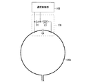
制御側無線通信装置300は、ここでは一例として、天板34における被検体Pが載置される面(以下、天板34の上面という)側に8つ配置されている。被検体Pは例えば、天板34の幅方向(図1のX軸方向)において中央に載置される。従って、この例では制御側無線通信装置300は、天板34の幅方向の両端側においてそれぞれ、天板34の長手方向(Z軸方向)に沿った列状に離散して4つずつ配置されている。   As an example, eight control-side wireless communication apparatuses 300 are arranged on the surface of the top plate 34 on which the subject P is placed (hereinafter referred to as the top surface of the top plate 34). For example, the subject P is placed in the center in the width direction of the top plate 34 (X-axis direction in FIG. 1). Therefore, in this example, the control-side wireless communication devices 300 are arranged in a discrete manner in rows along the longitudinal direction (Z-axis direction) of the top plate 34 on both ends in the width direction of the top plate 34. ing.

また、制御側無線通信装置300は、その筐体302(後述の図3参照)が天板34の上面の直下に埋設され、その固定板320(後述の図3参照)が天板34の上面から露出している。コイル側無線通信装置200Aは、固定板320に嵌合されることで、制御側無線通信装置300に対して離脱自在に固定される。   The control-side wireless communication apparatus 300 has a casing 302 (see FIG. 3 described later) embedded directly below the top surface of the top plate 34, and a fixed plate 320 (see FIG. 3 described later) as the top surface of the top plate 34. Is exposed from. The coil side wireless communication device 200 </ b> A is fixed to the control side wireless communication device 300 in a detachable manner by being fitted to the fixing plate 320.

従って、RFコイル装置が被検体Pのどの部分に装着されても、コイル側無線通信装置200Aを最も近くの制御側無線通信装置300に対して近接固定すればよい。本実施形態では胸部用のRFコイル装置100Aの例であるが、この点は、他の部位用のRFコイル装置とコイル側無線通信装置200Aとの組み合わせの場合についても言える。このため、ケーブル102の長さを短くできる。   Therefore, no matter what part of the subject P the RF coil device is attached to, the coil-side radio communication device 200A may be fixed in proximity to the nearest control-side radio communication device 300. Although this embodiment is an example of the RF coil device 100A for the chest, this point can also be said for the combination of the RF coil device for other regions and the coil-side radio communication device 200A. For this reason, the length of the cable 102 can be shortened.

なお、制御側無線通信装置300の数や配置箇所は、図2の態様(天板34内部)に限定されるものではない。制御側無線通信装置300は、例えば天板34上やガントリ21上に露出して配置してもよいし、ガントリ21内部に配置してもよいし、寝台32に対して配置してもよい。   In addition, the number and arrangement | positioning location of the control side radio | wireless communication apparatus 300 are not limited to the aspect (inside the top plate 34) of FIG. For example, the control-side wireless communication device 300 may be disposed so as to be exposed on the top plate 34 or the gantry 21, disposed inside the gantry 21, or disposed on the bed 32.

図3は、コイル側無線通信装置200Aを制御側無線通信装置300に対して固定する方法の一例を示す断面模式図である。図3(A)に示すように、コイル側無線通信装置200Aの筐体202上には、例えば2つの突起220が形成されている。   FIG. 3 is a schematic cross-sectional view illustrating an example of a method for fixing the coil-side wireless communication device 200 </ b> A to the control-side wireless communication device 300. As shown in FIG. 3A, for example, two protrusions 220 are formed on the casing 202 of the coil-side wireless communication device 200A.

突起220は、コイル側無線通信装置200Aの差し込み及び取り外しを容易にするため、例えば横断面が半円状に形成されている。一般に、突起220の表面の起伏が激しい構造よりも、滑らかに面取りされている方がコイル側無線通信装置200Aの差し込みが容易だからである。突起220は、例えば球面状であってもよいし、円筒をその軸方向に沿って半分に分割した形状でもよい。   In order to facilitate insertion and removal of the coil-side wireless communication device 200A, the protrusion 220 has, for example, a semicircular cross section. This is because the coil-side radio communication device 200A is generally easier to insert when the chamfered surface is smoother than a structure in which the surface of the protrusion 220 is rough. The protrusion 220 may have a spherical shape, for example, or may have a shape obtained by dividing a cylinder in half along the axial direction thereof.

ここでは一例として、突起220を含む筐体202は、変形しない非磁性体の材料で形成されているものとする。非磁性体の材料で形成することで、誘導電界を介した無線通信への影響を確実に回避できる。   Here, as an example, it is assumed that the housing 202 including the protrusions 220 is formed of a non-magnetic material that does not deform. By forming the non-magnetic material, it is possible to reliably avoid the influence on the wireless communication via the induction electric field.

制御側無線通信装置300は、その筐体302の両側の側面に対して例えば接着などにより固定された2つの固定板320を有する。各固定板320は、例えば略平板状であり、互いに対向するように配置されている。各固定板320は、図3(C)に示すように、コイル側無線通信装置200Aを嵌合させる形状である。即ち、2つの固定板320において、互いに対向する面には、突起220に対応する位置に、突起220を嵌合させる窪み部320aがそれぞれ面取りされている(図3(A)参照)。   The control-side wireless communication apparatus 300 includes two fixing plates 320 that are fixed to the side surfaces on both sides of the casing 302 by, for example, adhesion. Each fixed plate 320 has, for example, a substantially flat plate shape, and is arranged to face each other. As shown in FIG. 3C, each fixing plate 320 has a shape in which the coil-side wireless communication device 200A is fitted. That is, the two fixing plates 320 are chamfered on the surfaces facing each other at the positions corresponding to the protrusions 220 so as to fit the protrusions 220a (see FIG. 3A).

また、各固定板320において、その先端側(筐体302とは反対側)は、コイル側無線通信装置200Aを差し込み易くするために、斜めに面取りされている。固定板320については、図3(B)に示す程度の湾曲が可能な非磁性体の弾性材料で形成することが望ましい。かかる材料としては、例えば、プラスチックや合成樹脂などが挙げられる。非磁性体の材料で形成する理由は、前述同様である。   Further, in each fixing plate 320, the tip side (the side opposite to the housing 302) is chamfered obliquely so that the coil-side wireless communication device 200A can be easily inserted. The fixing plate 320 is preferably formed of a nonmagnetic elastic material capable of bending to the extent shown in FIG. Examples of such materials include plastics and synthetic resins. The reason for forming the non-magnetic material is the same as described above.

制御側無線通信装置300は、天板34の上面から、例えば間隔Dだけ奥に埋設されている(図3(C)の矢印参照)。間隔Dは、誘導電界を介した無線通信が可能な間隔である。天板34の上面には、固定板320を挿通させる溝が形成されており、この溝を介して、固定板320が天板34の上面から突出している。   The control-side wireless communication device 300 is embedded from the upper surface of the top plate 34, for example, at a depth D (see the arrow in FIG. 3C). The interval D is an interval in which wireless communication via an induction electric field is possible. A groove through which the fixing plate 320 is inserted is formed on the top surface of the top plate 34, and the fixing plate 320 protrudes from the top surface of the top plate 34 through this groove.

上記構成では、図3(A)の状態から、コイル側無線通信装置200Aが制御側無線通信装置300に差し込まれる。このとき、図3(B)に示すように、各固定板320は一時的に互いに離れる方向に曲がる。これは、コイル側無線通信装置200Aの両側の突起220間の最長幅が、両固定板320の最短幅よりも、大きいためである。   In the above configuration, the coil-side wireless communication device 200A is inserted into the control-side wireless communication device 300 from the state of FIG. At this time, as shown in FIG. 3B, the fixing plates 320 are temporarily bent in directions away from each other. This is because the longest width between the protrusions 220 on both sides of the coil-side radio communication device 200 </ b> A is larger than the shortest width of both the fixing plates 320.

そして、コイル側無線通信装置200Aの筺体220の底面が天板34の上面に接する位置において、両側の突起220がそれぞれ窪み部320aに嵌合され、各固定板320は、形状復元力により元の形状(図3(A)の形状)に戻る。これにより、コイル側無線通信装置200Aは、天板34上で制御側無線通信装置300に対して離脱自在に固定される。   Then, at the position where the bottom surface of the casing 220 of the coil side wireless communication device 200A is in contact with the top surface of the top plate 34, the protrusions 220 on both sides are fitted into the recessed portions 320a, and each fixing plate 320 is restored to its original shape by the shape restoring force. Return to the shape (the shape of FIG. 3A). As a result, the coil-side wireless communication device 200A is detachably fixed to the control-side wireless communication device 300 on the top plate 34.

ここで、コイル側無線通信装置200Aは、その底面側(上記固定時における制御側無線通信装置300側)において、アンテナ206a〜206dを有する。また、制御側無線通信装置は、その上面側(上記固定時におけるコイル側無線通信装置200A側)において、アンテナ306a〜306dを有する。アンテナ306a〜306dは、アンテナ206a〜206dとそれぞれ一対となるものである(計4対)。これらの内、少なくともアンテナ206a−306aは、例えば後述の誘導電界結合型カプラである。   Here, the coil-side wireless communication device 200A has antennas 206a to 206d on the bottom surface side (the control-side wireless communication device 300 side at the time of fixing). In addition, the control-side wireless communication device has antennas 306a to 306d on the upper surface side (the coil-side wireless communication device 200A side when fixed). The antennas 306a to 306d are paired with the antennas 206a to 206d (four pairs in total). Among these, at least the antennas 206a to 306a are, for example, inductive electric field coupling couplers described later.

そして、上記のようにコイル側無線通信装置200Aと制御側無線通信装置300とが互いに近接固定された状態において、アンテナ206a〜206dは、アンテナ306a〜306dにそれぞれ対向する位置に配置される。撮像が終了した場合には、コイル側無線通信装置200Aを天板34から離すように固定板320から抜き外せばよい。   In the state where the coil side wireless communication apparatus 200A and the control side wireless communication apparatus 300 are fixed in proximity to each other as described above, the antennas 206a to 206d are disposed at positions facing the antennas 306a to 306d, respectively. When the imaging is completed, the coil-side wireless communication device 200A may be removed from the fixed plate 320 so as to be separated from the top plate 34.

なお、上記のような嵌合は、コイル側無線通信装置200Aの固定方法の一例にすぎず、離脱自在な固定方法については、他の方法でもよい。例えば、面ファスナーのオス側及びメス側の内、一方を天板34の上面に固定し、他方をコイル側無線通信装置200Aの底面に固定してもよい。制御側無線通信装置300の上面が天板34の上面に露出する場合には、面ファスナーのオス側及びメス側の一方を御側無線通信装置300の上面に固定してもよい。   The fitting as described above is merely an example of a fixing method of the coil-side wireless communication device 200A, and other methods may be used for the detachable fixing method. For example, one of the male and female sides of the hook-and-loop fastener may be fixed to the top surface of the top plate 34, and the other may be fixed to the bottom surface of the coil-side radio communication device 200A. When the upper surface of the control-side wireless communication device 300 is exposed on the upper surface of the top plate 34, one of the male side and the female side of the hook-and-loop fastener may be fixed to the upper surface of the control-side wireless communication device 300.

コイル側無線通信装置200Aと制御側無線通信装置300との間では、誘導電界を介した近接無線通信が実行される。誘導電界とは、磁束密度の時間変化によって生じる電界である。誘導電界を介した近接無線通信としては、例えば、誘導電界結合型カプラをアンテナとして用いるトランスファージェット(TransferJet:登録商標)などを用いればよい(例えば特開2010−147922号公報参照)。   Proximity wireless communication via an induction electric field is executed between the coil-side wireless communication device 200A and the control-side wireless communication device 300. An induced electric field is an electric field generated by a change in magnetic flux density over time. As the close proximity wireless communication via the induction electric field, for example, a transfer jet (TransferJet: registered trademark) using an induction electric field coupling type coupler as an antenna may be used (see, for example, Japanese Patent Application Laid-Open No. 2010-147922).

より詳細には、誘導電界結合型カプラは、結合電極、共振スタブ、グランドなどを有する(図示せず)。誘導電界結合型カプラの送信側の共振スタブに電気信号が入力されると、結合電極に電荷が蓄積され、その電荷と同等の仮想電荷がグランドに発生する。それらの電荷によって微小電気双極子が構成され、この微小電気双極子が送信側アンテナとして機能する。即ち、微小電気双極子が発生する縦波の誘導電界により、受信側にデータが転送される。進行方向と平行に振動する縦波は、アンテナの向きに依存しないため、安定したデータ転送を実現できる。   More specifically, the induction electric field coupling type coupler has a coupling electrode, a resonant stub, a ground, and the like (not shown). When an electrical signal is input to the resonant stub on the transmission side of the inductive field coupled coupler, charges are accumulated in the coupling electrode, and virtual charges equivalent to the charges are generated on the ground. These electric charges form a minute electric dipole, and this minute electric dipole functions as a transmitting antenna. That is, data is transferred to the receiving side by a longitudinal wave induced electric field generated by a minute electric dipole. Longitudinal waves that oscillate in parallel with the traveling direction do not depend on the direction of the antenna, so that stable data transfer can be realized.

但し、送信側と受信側とを離しすぎると、両者が電磁的に結合されないため、データ送信ができない。誘導電界結合型カプラにより形成される誘導電界は、離れると急激に減衰するからである。   However, if the transmitting side and the receiving side are separated too much, the two cannot be electromagnetically coupled, and data transmission cannot be performed. This is because the induction electric field formed by the induction electric field coupling type coupler is abruptly attenuated when separated.

図3では各構成要素を区別するために、アンテナ206a〜206dを互いに離間して配置すると共に、アンテナ306a〜306dを互いに離間して配置しているが、離間して配置しなくとも、4つの無線通信経路同士の干渉を避けることができる。   In FIG. 3, in order to distinguish each component, the antennas 206a to 206d are arranged apart from each other and the antennas 306a to 306d are arranged apart from each other. Interference between wireless communication paths can be avoided.

具体的には、アンテナ206a−306a間、アンテナ206b−306b間、アンテナ206c−306c間、アンテナ206d−306d間で、無線周波数を分離すればよい(周波数値を大きく離せばよい)。このとき、各無線通信経路では、被検体Pに送信されるRFパルスの中心周波数の整数分の一となる周波数を避けることが望ましい。   Specifically, the radio frequency may be separated between the antennas 206a and 306a, between the antennas 206b and 306b, between the antennas 206c and 306c, and between the antennas 206d and 306d (the frequency value may be greatly separated). At this time, in each wireless communication path, it is desirable to avoid a frequency that is an integral fraction of the center frequency of the RF pulse transmitted to the subject P.

制御側無線通信装置300の設置箇所は、天板34の上面から深すぎないことが望ましい。制御側無線通信装置300のアンテナ306a〜306dの位置が深すぎると、送信側及び受信側のアンテナ206a〜206d、306a〜306dが互いに電磁的に結合される程度に、両者の間隔D(図3(C)参照)を近接させることができない。その場合、誘導電界を介した無線通信が困難となる。即ち、制御側無線通信装置300は、電磁的に結合される程度にコイル側無線通信装置200Aに対して近接固定することが可能な位置に配置することが望ましい。   It is desirable that the installation location of the control-side wireless communication device 300 is not too deep from the top surface of the top plate 34. If the positions of the antennas 306a to 306d of the control-side wireless communication apparatus 300 are too deep, the distance D between the antennas 206a to 206d and 306a to 306d on the transmission side and the reception side is electromagnetically coupled to each other (FIG. 3). (See (C)) cannot be brought close to each other. In that case, wireless communication via an induced electric field becomes difficult. That is, it is desirable that the control-side wireless communication device 300 is disposed at a position where the control-side wireless communication device 300 can be fixed in proximity to the coil-side wireless communication device 200A to the extent that it is electromagnetically coupled.

なお、コイル側無線通信装置200A側の電気双極子自体(アンテナ)と、制御側無線通信装置300側の電気双極子自体(アンテナ)とを直接接触させない限り、コイル側無線通信装置200A側のアンテナを覆う筐体と、制御側無線通信装置300側のアンテナを覆う筐体とを接触させても構わない。送信側のアンテナと、受信側のアンテナとの間に誘導電界が生じる間隔Dを確保できればよいからである。従って、制御側無線通信装置300は、そのアンテナ側の面が、天板34の上面に揃うように露出していてもよい。   As long as the electric dipole itself (antenna) on the coil-side radio communication apparatus 200A side and the electric dipole itself (antenna) on the control-side radio communication apparatus 300 side are not in direct contact, the antenna on the coil-side radio communication apparatus 200A side is used. And a housing that covers the antenna on the control-side wireless communication apparatus 300 side may be brought into contact with each other. This is because it is only necessary to secure a gap D in which an induced electric field is generated between the transmitting antenna and the receiving antenna. Therefore, the control-side wireless communication device 300 may be exposed so that the antenna-side surface is aligned with the top surface of the top plate 34.

図4は、RFコイル装置100Aのコイル素子106a〜106fで検出されたMR信号の送信に関わる各部の機能を模式的に示すブロック図である。以下、図4の上側から順に構成要素を説明する。即ち、RFコイル装置100Aのカバー部材104、コイル側無線通信装置200A、制御側無線通信装置300、MRI装置20Aの制御側、の順に説明する。   FIG. 4 is a block diagram schematically showing the function of each part related to transmission of MR signals detected by the coil elements 106a to 106f of the RF coil device 100A. Hereinafter, components will be described in order from the upper side of FIG. That is, the cover member 104 of the RF coil device 100A, the coil side wireless communication device 200A, the control side wireless communication device 300, and the control side of the MRI device 20A will be described in this order.

まず、カバー部材104内には、前述の選択制御部108と、前述の複数のコイル素子106a〜106fと、A/D変換器140a〜140fと、P/S変換器(Parallel/Serial Converter)144と、充電池BAと、データ保護部150とが配置される。但し、図4では煩雑となるので、コイル素子106c〜106f、及び、A/D変換器140c〜140fを図示していない。   First, in the cover member 104, the selection control unit 108, the plurality of coil elements 106a to 106f, the A / D converters 140a to 140f, and a P / S converter (Parallel / Serial Converter) 144 are provided. A rechargeable battery BA and a data protection unit 150 are arranged. However, since it becomes complicated in FIG. 4, the coil elements 106c to 106f and the A / D converters 140c to 140f are not shown.

データ保護部150は、記憶制御部152と、電界シールド156と、電界シールド156内の記憶素子160a〜160fとを有する。但し、図4では煩雑となるので、記憶素子160c〜160fを図示していない。即ち、この例では、記憶素子(160a〜160f)の数は、A/D変換器(140a〜140f)の数、及び、コイル素子(106a〜106f)の数と同数である。   The data protection unit 150 includes a storage control unit 152, an electric field shield 156, and storage elements 160a to 160f in the electric field shield 156. However, since it becomes complicated in FIG. 4, the storage elements 160 c to 160 f are not shown. That is, in this example, the number of storage elements (160a to 160f) is the same as the number of A / D converters (140a to 140f) and the number of coil elements (106a to 106f).

各A/D変換器140a〜140fは、各コイル素子106a〜106fにそれぞれ対応し、記憶素子160a〜160fは、各A/D変換器140a〜140fにそれぞれ対応する。各コイル素子106a〜106fで検出されたMR信号は、対応するA/D変換器140a〜140fでそれぞれデジタル化されてから、対応する記憶素子160a〜160fにそれぞれ記憶される。   The A / D converters 140a to 140f correspond to the coil elements 106a to 106f, respectively, and the storage elements 160a to 160f correspond to the A / D converters 140a to 140f, respectively. MR signals detected by the coil elements 106a to 106f are digitized by the corresponding A / D converters 140a to 140f, respectively, and then stored in the corresponding storage elements 160a to 160f.

各記憶素子160a〜160fは、誘導電界を介してコイル側無線通信装置200Aから制御側無線通信装置300に無線送信されるMR信号のデータをバックアップする。このため、コイル側無線通信装置200Aから制御側無線通信装置300にMR信号が正常に送信されなかった場合、記憶素子160a〜160f内の記憶データが用いられる。   Each of the storage elements 160a to 160f backs up MR signal data wirelessly transmitted from the coil-side wireless communication device 200A to the control-side wireless communication device 300 via the induction electric field. For this reason, when the MR signal is not normally transmitted from the coil side wireless communication apparatus 200A to the control side wireless communication apparatus 300, the stored data in the storage elements 160a to 160f is used.

従って、記憶素子(160a〜160f)の最大数としては、アンテナとして機能するコイル素子(106a〜106f)と同数が望ましい。但し、記憶素子の数は、上記態様に限定されるものではなく、例えば1つでもよい。或いは、記憶素子の数は、コイル素子の数の半数とし、各記憶素子に対して、2つのコイル素子で検出されたMR信号をそれぞれ記憶させてもよい。   Accordingly, the maximum number of memory elements (160a to 160f) is preferably the same as the number of coil elements (106a to 106f) functioning as antennas. However, the number of memory elements is not limited to the above aspect, and may be one, for example. Alternatively, the number of memory elements may be half of the number of coil elements, and MR signals detected by two coil elements may be stored in each memory element.

記憶素子160a〜160fとしては、MR信号の送信、受信に対する影響を回避するため、非磁気的にデータの読み書きが可能なものが望ましい。従って、記憶素子160a〜160fとしては、例えば、フラッシュメモリやEEPROM(Electronically Erasable and Programmable Read Only Memory)などの半導体記憶素子を用いることができる。本実施形態では一例として、フラッシュメモリを用いるものとする。   As the storage elements 160a to 160f, it is desirable to be able to read / write data non-magnetically in order to avoid influence on transmission and reception of MR signals. Therefore, as the memory elements 160a to 160f, for example, a semiconductor memory element such as a flash memory or an EEPROM (Electronically Erasable and Programmable Read Only Memory) can be used. In this embodiment, a flash memory is used as an example.

但し、記憶素子160a〜160fについては、半導体記憶素子に限定されるものではない。例えば光ピックアップ装置をデータ保護部150内に搭載し、書き替え可能な小型の光ディスクに対して、レーザーによりデータの記録及び消去を実行してもよい。その場合、電界シールド156を省いてもよい。   However, the memory elements 160a to 160f are not limited to semiconductor memory elements. For example, an optical pickup device may be mounted in the data protection unit 150, and data recording and erasure may be performed with a laser on a rewritable small optical disk. In that case, the electric field shield 156 may be omitted.

また、記憶素子160a〜160fはそれぞれ、例えばUSB(Universal Serial Bus)などの接続ポートを有し、この接続ポートを介して、データ保護部150に対して離脱自在に接続可能である。また、記憶素子160a〜160fはそれぞれ、後述のデータ回収部600(図10参照)に対しても、離脱自在に接続可能である。   Each of the storage elements 160a to 160f has a connection port such as a USB (Universal Serial Bus), for example, and can be detachably connected to the data protection unit 150 via the connection port. Each of the storage elements 160a to 160f can be detachably connected to a data collection unit 600 (see FIG. 10) described later.

電界シールド156は、例えば、非磁性体であると共に導電性の高い金属により形成した筐体である。かかる金属としては、例えば真鍮や銅が挙げられる。なお、プラスチックなどの変形しない非磁性体を銅箔で覆うことで電界シールド156を形成してもよい。   The electric field shield 156 is, for example, a housing made of a nonmagnetic material and a highly conductive metal. Examples of such metal include brass and copper. Note that the electric field shield 156 may be formed by covering a non-deformable material such as plastic with a copper foil.

記憶制御部152は、各記憶素子160a〜160fに対するMR信号のデータの書き込み及び消去の動作を制御する。   The storage control unit 152 controls the operation of writing and erasing MR signal data to each of the storage elements 160a to 160f.

次に、コイル側無線通信装置200Aは、前述のアンテナ206a〜206dに加えて、データ送信部216と、参照信号受信部218と、ID送信部(Identification Information Transmitting Unit)222と、ゲート信号受信部224と、コイルL2とをさらに有する。   Next, in addition to the antennas 206a to 206d described above, the coil-side wireless communication device 200A includes a data transmission unit 216, a reference signal reception unit 218, an ID transmission unit (Identification Information Transmitting Unit) 222, and a gate signal reception unit. 224 and a coil L2.

図4において、ゲート信号受信部224−選択制御部108間の配線、コイルL2−充電池BA間の配線、参照信号受信部218−各A/D変換器140a〜140f間の配線、及び、P/S変換器144−データ送信部216間の配線等は、ケーブル102(図2参照)内に収納される。図4では煩雑となるので、ケーブル102を図示していない。   4, the wiring between the gate signal receiving unit 224 and the selection control unit 108, the wiring between the coil L2 and the rechargeable battery BA, the wiring between the reference signal receiving unit 218 and each of the A / D converters 140a to 140f, and P The wiring between the / S converter 144 and the data transmission unit 216 is accommodated in the cable 102 (see FIG. 2). In FIG. 4, the cable 102 is not shown because it is complicated.

また、コイル側無線通信装置200A内のコイルL2と、カバー部材104内の充電池BAとにより、電力受給部220が構成される。   The coil L2 in the coil-side wireless communication device 200A and the rechargeable battery BA in the cover member 104 constitute the power receiving unit 220.

次に、制御側無線通信装置300は、前述のアンテナ306a〜306dに加えて、データ受信部316と、参照信号送信部318と、電力供給部320と、ID受信部(Identification Information Receiving Unit)322と、ゲート信号送信部324とをさらに有する。また、電力供給部320は、コイルL1を有する。   Next, in addition to the antennas 306a to 306d, the control-side wireless communication apparatus 300 includes a data reception unit 316, a reference signal transmission unit 318, a power supply unit 320, and an ID reception unit (Identification Information Receiving Unit) 322. And a gate signal transmission unit 324. The power supply unit 320 includes a coil L1.

次に、MRI装置20Aの制御系は、図1に示した構成要素に加えて、周波数アップコンバージョン部402、パルス波形生成部404、固定周波数生成部406、可変周波数生成部408をさらに有する。また、RF受信器48は、周波数ダウンコンバージョン部410と、判定部412とを有する。   Next, the control system of the MRI apparatus 20A further includes a frequency up-conversion unit 402, a pulse waveform generation unit 404, a fixed frequency generation unit 406, and a variable frequency generation unit 408 in addition to the components shown in FIG. The RF receiver 48 includes a frequency down-conversion unit 410 and a determination unit 412.

第1の実施形態では一例として、コイル側無線通信装置200Aと制御側無線通信装置300との間には、充電用の誘導磁界が発生する領域と、4つの無線通信経路とが存在する。以下、これらについて順に説明する。   In the first embodiment, as an example, a region where a charging induction magnetic field is generated and four wireless communication paths exist between the coil-side wireless communication device 200A and the control-side wireless communication device 300. Hereinafter, these will be described in order.

コイルL2がコイルL1と電磁的に結合される程度に近接した範囲内にある場合、即ち、前述の図3(C)のようにコイル側無線通信装置200Aが制御側無線通信装置300に対して近接固定された場合を考える。この場合、電力供給部320がコイルL1に1次側電流を流すことで生じる誘導磁界により、コイルL2には起電力が発生する。この起電力によりコイルL2に2次側電流が流れ、充電池BAが充電される。   When the coil L2 is within a range close enough to be electromagnetically coupled to the coil L1, that is, as shown in FIG. 3C, the coil side wireless communication device 200A is connected to the control side wireless communication device 300. Consider the case where proximity is fixed. In this case, an electromotive force is generated in the coil L2 by an induced magnetic field generated when the power supply unit 320 causes the primary current to flow through the coil L1. Due to this electromotive force, a secondary current flows through the coil L2, and the rechargeable battery BA is charged.

電力受給部220は、不図示の配線を介して、コイル側無線通信装置200A内の各部やRFコイル装置100Aの各部に対して、上記のように充電された電力を供給する。ここで、コイルL1に流す1次側電流の周波数については、4つの無線通信経路の通信周波数から分離することが望ましい。これは、アンテナ206a〜206d、306a〜306d間の4つの無線通信経路の信号と、上記1次側電流及び2次側電流との干渉を避けるためである。   The power receiving unit 220 supplies the power charged as described above to each unit in the coil-side wireless communication device 200A and each unit of the RF coil device 100A via a wiring (not shown). Here, it is desirable to separate the frequency of the primary current flowing through the coil L1 from the communication frequencies of the four wireless communication paths. This is to avoid interference between signals on the four wireless communication paths between the antennas 206a to 206d and 306a to 306d and the primary side current and the secondary side current.

なお、RFコイル装置100Aの電力確保の方法としては、電力受給部220や電力供給部320の代わりに、RFコイル装置100Aの未使用期間中に充電される別の充電池をカバー部材104内に搭載してもよい。或いは、RFコイル装置100Aの未使用期間中に充電される別の充電池と、上記電力受給部220及び電力供給部320による電力供給とを併用してもよい。   In addition, as a method of securing the power of the RF coil device 100A, instead of the power receiving unit 220 or the power supply unit 320, another rechargeable battery charged during the unused period of the RF coil device 100A is placed in the cover member 104. May be installed. Alternatively, another rechargeable battery that is charged during the unused period of the RF coil device 100 </ b> A may be used in combination with power supply by the power receiving unit 220 and the power supply unit 320.

次に、4つの無線通信経路について説明する。誘導電界を介した無線通信は、少なくともアンテナ206a−306a間で行われるが、アンテナ206b−306b間やアンテナ206d−306d間で行われてもよい。   Next, the four wireless communication paths will be described. The wireless communication via the induction electric field is performed at least between the antennas 206a and 306a, but may be performed between the antennas 206b and 306b or between the antennas 206d and 306d.

第1に、アンテナ206c−306c間では、RFコイル装置100Aの識別情報がコイル側無線通信装置200Aから制御側無線通信装置300に無線送信される。具体的には例えば、上記識別情報がID送信部222に予め記憶されている。但し、RFコイル装置100Aの識別情報は、選択制御部108からケーブル102を介してコイル側無線通信装置200AのID送信部222に入力されてもよい。   First, between the antennas 206c and 306c, the identification information of the RF coil device 100A is wirelessly transmitted from the coil side wireless communication device 200A to the control side wireless communication device 300. Specifically, for example, the identification information is stored in advance in the ID transmission unit 222. However, the identification information of the RF coil device 100A may be input from the selection control unit 108 to the ID transmission unit 222 of the coil side wireless communication device 200A via the cable 102.

ID受信部322のアンテナ306cがID送信部222のアンテナ206cに近づくと、ID送信部222は、ID受信部322から無線送信される電力に基づいて動作する。即ち、ID送信部222は、上記識別情報をデジタル信号としてアンテナ206cからアンテナ306cに自動的に無線送信する。この識別情報の無線通信は、例えばICタグ(Integrated Circuit Tag)などに代表されるRFID(Radio Frequency Identification)と同様の手段でよい。   When the antenna 306 c of the ID reception unit 322 approaches the antenna 206 c of the ID transmission unit 222, the ID transmission unit 222 operates based on the power wirelessly transmitted from the ID reception unit 322. That is, the ID transmission unit 222 automatically wirelessly transmits the identification information as a digital signal from the antenna 206c to the antenna 306c. The wireless communication of this identification information may be the same means as RFID (Radio Frequency Identification) represented by, for example, an IC tag (Integrated Circuit Tag).

ID受信部322は、アンテナ306cで受信したRFコイル装置100Aの識別情報をシステム制御部52に入力する。これにより、胸部用RFコイル装置、肩用RFコイル装置などの各種RFコイル装置のどれが現在接続されているか等の情報がシステム制御部52により認識される。   The ID receiving unit 322 inputs the identification information of the RF coil device 100A received by the antenna 306c to the system control unit 52. As a result, the system control unit 52 recognizes information such as which of various RF coil devices such as a chest RF coil device and a shoulder RF coil device is currently connected.

第2に、アンテナ306d−206d間では、制御側無線通信装置300のゲート信号送信部324からコイル側無線通信装置200Aのゲート信号受信部224に対して、ゲート信号が撮像中において継続的に無線送信される。   Second, between the antennas 306d to 206d, the gate signal is continuously wirelessly captured from the gate signal transmission unit 324 of the control-side wireless communication device 300 to the gate signal reception unit 224 of the coil-side wireless communication device 200A during imaging. Sent.

より詳細には、RFコイル装置100A内の各コイル素子106のオンオフを切り替えるスイッチとして、例えば、PINダイオード(p-intrinsic-n Diode)を含むアクティブトラップ回路170などが用いられる(後述の図6参照)。ゲート信号は、例えば、トラップ回路のインピーダンスの切替タイミングを規定する信号(上記スイッチの制御信号)である。なお、ゲート信号送信部324からゲート信号受信部224にトリガ信号が送信され、ゲート信号受信部224内でトリガ信号に基づいてゲート信号が生成される構成でもよい。   More specifically, for example, an active trap circuit 170 including a PIN diode (p-intrinsic-n Diode) is used as a switch for switching on and off each coil element 106 in the RF coil device 100A (see FIG. 6 described later). ). The gate signal is, for example, a signal (control signal for the switch) that defines the impedance switching timing of the trap circuit. The gate signal transmission unit 324 may transmit a trigger signal to the gate signal reception unit 224, and the gate signal may be generated based on the trigger signal in the gate signal reception unit 224.

RFパルスが被検体Pに送信される期間では、ゲート信号送信部324、アンテナ306d、206d、ゲート信号受信部224を介してRFコイル装置100Aに入力されるゲート信号は、通常、オンレベルにされる。ゲート信号がオンレベルの期間では、上記スイッチはオフ状態となり、各コイル素子106a〜106fは、ループが途切れた状態となり、MR信号を検出できない。   During the period in which the RF pulse is transmitted to the subject P, the gate signal input to the RF coil device 100A via the gate signal transmission unit 324, the antennas 306d and 206d, and the gate signal reception unit 224 is normally set to the on level. The During the period when the gate signal is on level, the switch is turned off, and each of the coil elements 106a to 106f is in a state where the loop is interrupted, and the MR signal cannot be detected.

RFパルスが被検体Pに送信される期間を除く期間では、オフレベルのゲート信号が無線送信される。ゲート信号がオフレベルの期間では、上記スイッチはオン状態となり、各コイル素子106a〜106fは、MR信号を検出できる。このようなコイル素子106a〜106fのオンオフの切り替えにより、被検体PにRFパルスを送信する送信用RFコイル28と、MR信号を受信するコイル素子106a〜106fとの間のカップリングが防止される。   In the period excluding the period during which the RF pulse is transmitted to the subject P, the off-level gate signal is wirelessly transmitted. During the period when the gate signal is at the off level, the switch is turned on, and each of the coil elements 106a to 106f can detect the MR signal. Such on / off switching of the coil elements 106a to 106f prevents coupling between the transmitting RF coil 28 that transmits an RF pulse to the subject P and the coil elements 106a to 106f that receive the MR signal. .

第3に、アンテナ306b−206b間では、制御側無線通信装置300の参照信号送信部318からコイル側無線通信装置200Aの参照信号受信部218に対して、デジタルの参照信号がスキャンの始めに無線送信される。   Third, between the antennas 306b and 206b, a digital reference signal is wirelessly transmitted from the reference signal transmitting unit 318 of the control-side wireless communication device 300 to the reference signal receiving unit 218 of the coil-side wireless communication device 200A at the beginning of the scan. Sent.

具体的には、参照信号は、MR信号の送信側であるコイル側無線通信装置200Aと、固定周波数生成部406をベースとしたシステムの基準周波数とを同期させる信号である。参照信号送信部318は、固定周波数生成部406から入力される基準クロック信号に対して変調、周波数変換、増幅、フィルタリング等の処理を施すことで、参照信号を生成する。   Specifically, the reference signal is a signal that synchronizes the coil-side radio communication device 200 </ b> A that is the transmission side of the MR signal and the reference frequency of the system based on the fixed frequency generation unit 406. The reference signal transmission unit 318 generates a reference signal by performing processing such as modulation, frequency conversion, amplification, and filtering on the reference clock signal input from the fixed frequency generation unit 406.

第1の実施形態では一例として、参照信号受信部218は、一定周波数の基準クロック信号を生成する水晶発振器などを有し、参照信号送信部318と同様にして参照信号を生成可能である。即ち、参照信号受信部218は、スキャンの始めのみ参照信号を受信後、受信した参照信号内の立ち上がりや立ち下がり等のタイミングに適合させて、参照信号の生成を開始する。なお、スキャンの始めに参照信号受信部218が受信する参照信号には、後述のA/D変換開始信号(トリガ信号)が重畳されている。   In the first embodiment, as an example, the reference signal receiving unit 218 includes a crystal oscillator that generates a reference clock signal having a constant frequency, and can generate a reference signal in the same manner as the reference signal transmission unit 318. That is, after receiving the reference signal only at the beginning of the scan, the reference signal receiving unit 218 starts generating the reference signal in accordance with the timing of rising or falling in the received reference signal. Note that an A / D conversion start signal (trigger signal) described later is superimposed on the reference signal received by the reference signal receiving unit 218 at the beginning of the scan.

参照信号受信部218は、生成した参照信号を各A/D変換器140a〜140fに対して、スキャン中に継続的に入力する。これにより、コイル側無線通信装置200Aと制御側無線通信装置300との間に通信阻害が生じた場合にも、コイル素子(106a〜106f)で検出されたMR信号は、A/D変換器140a〜140fで正常にA/D変換されてから、記憶素子160a〜160fにバックアップされる。   The reference signal receiving unit 218 continuously inputs the generated reference signal to the A / D converters 140a to 140f during scanning. Thereby, even when communication obstruction occurs between the coil side radio communication apparatus 200A and the control side radio communication apparatus 300, the MR signal detected by the coil elements (106a to 106f) is converted into the A / D converter 140a. After being normally A / D converted at ~ 140f, it is backed up to the storage elements 160a ~ 160f.

但し、参照信号受信部218内で参照信号を生成しなくてもよい。アンテナ306b−206b間において、参照信号送信部318から参照信号受信部218に参照信号を撮像中に継続的に無線送信してもよい。   However, the reference signal may not be generated in the reference signal receiving unit 218. Between the antennas 306b and 206b, the reference signal may be continuously transmitted from the reference signal transmission unit 318 to the reference signal reception unit 218 during imaging.

固定周波数生成部406は、一定周波数の基準クロック信号を生成する。固定周波数生成部406は、基準クロック信号を生成するために、例えば安定度の高い水晶発振器などを有する。固定周波数生成部406は、参照信号送信部318及び可変周波数生成部408に基準クロック信号を入力する。また、固定周波数生成部406は、画像再構成部56やパルス波形生成部404などのMRI装置20A内でクロック同期が行われる箇所にも基準クロック信号を入力する。   The fixed frequency generation unit 406 generates a reference clock signal having a constant frequency. The fixed frequency generation unit 406 includes, for example, a highly stable crystal oscillator in order to generate a reference clock signal. The fixed frequency generation unit 406 inputs the reference clock signal to the reference signal transmission unit 318 and the variable frequency generation unit 408. In addition, the fixed frequency generation unit 406 also inputs a reference clock signal to a place where clock synchronization is performed in the MRI apparatus 20A such as the image reconstruction unit 56 and the pulse waveform generation unit 404.

可変周波数生成部408は、PLL(Phase-Locked Loop:位相同期回路)、DDS(Direct Digital Synthesizer:デジタル直接合成発振器)、ミキサなどを有する。可変周波数生成部408は、上記の基準クロック信号に基づいて動作する。可変周波数生成部408は、RFパルスの中心周波数としてシステム制御部52から入力される設定値に一致する可変周波数のローカル信号(クロック信号)を生成する。   The variable frequency generation unit 408 includes a PLL (Phase-Locked Loop), a DDS (Direct Digital Synthesizer), a mixer, and the like. The variable frequency generation unit 408 operates based on the reference clock signal. The variable frequency generation unit 408 generates a variable frequency local signal (clock signal) that matches the set value input from the system control unit 52 as the center frequency of the RF pulse.

そのために、システム制御部52は、プレスキャンの前にRFパルスの中心周波数の初期値を可変周波数生成部408に入力する。また、システム制御部52は、プレスキャン後にはRFパルスの中心周波数の補正値を可変周波数生成部408に入力する。   For this purpose, the system control unit 52 inputs an initial value of the center frequency of the RF pulse to the variable frequency generation unit 408 before the pre-scan. Further, the system control unit 52 inputs the correction value of the center frequency of the RF pulse to the variable frequency generation unit 408 after the prescan.

可変周波数生成部408は、周波数ダウンコンバージョン部410及び周波数アップコンバージョン部402に対して、上記の可変周波数のローカル信号を入力する。   The variable frequency generation unit 408 inputs the variable frequency local signal to the frequency down conversion unit 410 and the frequency up conversion unit 402.

また、カバー部材104内のA/D変換器140a〜140fにおけるサンプリングのタイミングを決めるトリガ信号(A/D変換開始信号)が、システム制御部52から参照信号送信部318に入力される。ここでのサンプリングとは、例えば、アナログ信号の強さを一定時間ごとに採取し、デジタル記録が可能な形にすることである。ここでは一例として、参照信号送信部318は、トリガ信号を参照信号に重畳することで参照信号及びトリガ信号の双方を、スキャンの始めのみ参照信号受信部218に無線送信する。   In addition, a trigger signal (A / D conversion start signal) that determines the sampling timing in the A / D converters 140 a to 140 f in the cover member 104 is input from the system control unit 52 to the reference signal transmission unit 318. Sampling here refers to, for example, taking the strength of an analog signal at regular intervals and making it digitally recordable. Here, as an example, the reference signal transmission unit 318 wirelessly transmits both the reference signal and the trigger signal to the reference signal reception unit 218 only at the start of scanning by superimposing the trigger signal on the reference signal.

第4に、アンテナ206a−306a間では、コイル側無線通信装置200Aのデータ送信部216から制御側無線通信装置300のデータ受信部316に対して、デジタルのMR信号が誘導電界を介して無線送信される。   Fourth, between the antennas 206a and 306a, a digital MR signal is wirelessly transmitted from the data transmission unit 216 of the coil-side wireless communication device 200A to the data reception unit 316 of the control-side wireless communication device 300 via an induced electric field. Is done.

具体的には、受信用に選択されたコイル素子(106a〜106fの少なくとも1つ)で検出されたアナログのMR信号は、対応するA/D変換器(140a〜140fのいずれか)に入力され、デジタル信号に変換される。このとき、各A/D変換器(140a〜140f)には、参照信号受信部218から参照信号及びトリガ信号が入力される。従って、各A/D変換器(140a〜140f)は、トリガ信号が送信されたタイミングに同期して、参照信号(サンプリングクロック信号)に基づいてサンプリング及び量子化を開始する。   Specifically, an analog MR signal detected by a coil element (at least one of 106a to 106f) selected for reception is input to a corresponding A / D converter (any of 140a to 140f). Converted into a digital signal. At this time, a reference signal and a trigger signal are input from the reference signal receiving unit 218 to each A / D converter (140a to 140f). Accordingly, each A / D converter (140a to 140f) starts sampling and quantization based on the reference signal (sampling clock signal) in synchronization with the timing at which the trigger signal is transmitted.

各A/D変換器(140a〜140f)は、対応する記憶素子(160a〜160fのいずれか)と、P/S変換器144とに対して、デジタルのMR信号を入力する。即ち、A/D変換器140aは、記憶素子160a及びP/S変換器144に対して、コイル素子106aで検出されてからデジタル化されたMR信号を入力する。同様に、A/D変換器140bは、記憶素子160b及びP/S変換器144に対して、コイル素子106bで検出されてからデジタル化されたMR信号を入力する。A/D変換器140c〜140fについても同様である。   Each A / D converter (140a to 140f) inputs a digital MR signal to the corresponding storage element (any one of 160a to 160f) and the P / S converter 144. That is, the A / D converter 140a inputs the MR signal digitized after being detected by the coil element 106a to the storage element 160a and the P / S converter 144. Similarly, the A / D converter 140b inputs the MR signal digitized after being detected by the coil element 106b to the storage element 160b and the P / S converter 144. The same applies to the A / D converters 140c to 140f.

但し、MR信号の受信用に選択されていないコイル素子(106a〜106f)が存在する場合、当該非選択のコイル素子に対応するA/D変換器(140a〜140f)及び記憶素子(160a〜160f)は動作しない。   However, when there are coil elements (106a to 106f) that are not selected for receiving MR signals, the A / D converters (140a to 140f) and the storage elements (160a to 160f) corresponding to the non-selected coil elements. ) Does not work.

P/S変換器144は、入力された単数又は複数のMR信号を無線送信用にパラレル信号からシリアル信号に変換し、このシリアル信号をケーブル102経由でコイル側無線通信装置200Aのデータ送信部216に入力する。第1の実施形態の例では、MR信号の送信用のアンテナは、アンテナ206aの1つだけだからである。   The P / S converter 144 converts one or more input MR signals from a parallel signal to a serial signal for wireless transmission, and the serial signal is transmitted via the cable 102 to the data transmission unit 216 of the coil-side wireless communication device 200A. To enter. This is because in the example of the first embodiment, there is only one antenna 206a for transmitting MR signals.

但し、本実施形態はシリアル信号として無線送信する態様に限定されるものではない。例えばMR信号の送信用及び受信用のアンテナ数を増やす等により、パラレル信号のまま無線送信する構成にしてもよい。   However, the present embodiment is not limited to the aspect of wireless transmission as a serial signal. For example, a configuration may be adopted in which the number of antennas for transmitting and receiving MR signals is increased and wireless transmission is performed with parallel signals.

データ送信部216は、入力されたシリアルのMR信号に対し、誤り訂正符号化、インタリーブ、変調、周波数変換、増幅、フィルタリングなどの処理を施すことで、(シリアル信号かつデジタル信号である)無線送信用のMR信号を生成する。データ送信部216は、無線送信用のMR信号をアンテナ206aからアンテナ306aに無線送信する。   The data transmission unit 216 performs processing such as error correction coding, interleaving, modulation, frequency conversion, amplification, filtering, etc. on the input serial MR signal, thereby performing wireless transmission (which is a serial signal and a digital signal). A trusted MR signal is generated. The data transmission unit 216 wirelessly transmits an MR signal for wireless transmission from the antenna 206a to the antenna 306a.

データ受信部316は、アンテナ306aにより受信したMR信号に対して、増幅、周波数変換、復調、逆インタリーブ、誤り訂正復号等の処理を施す。これにより、データ受信部316は、無線送信用のMR信号から元のデジタルのMR信号を抽出し、抽出したMR信号をRF受信器48の周波数ダウンコンバージョン部410に入力する。   The data receiving unit 316 performs processing such as amplification, frequency conversion, demodulation, deinterleaving, and error correction decoding on the MR signal received by the antenna 306a. As a result, the data receiving unit 316 extracts the original digital MR signal from the MR signal for radio transmission, and inputs the extracted MR signal to the frequency down-conversion unit 410 of the RF receiver 48.

周波数ダウンコンバージョン部410は、可変周波数生成部408から入力されるローカル信号を、データ受信部316から入力されるMR信号に乗算し、さらにフィルタリングによって所望の信号帯域のみを通過させる。これにより、周波数ダウンコンバージョン部410は、MR信号を周波数変換(ダウンコンバージョン)し、周波数が低くされたMR信号を判定部412に入力する。   The frequency down-conversion unit 410 multiplies the local signal input from the variable frequency generation unit 408 by the MR signal input from the data reception unit 316, and further passes only a desired signal band by filtering. Thereby, the frequency down-conversion unit 410 frequency-converts (down-converts) the MR signal and inputs the MR signal whose frequency is lowered to the determination unit 412.

判定部412は、周波数が低くされたMR信号に所定の信号処理を施すことで、MR信号の生データを生成し、MR信号の生データに基づいて送信不良の有無を判定する。判定部412は、送信不良有りと判定した場合、データのどの部分が送信不良(欠落等)であるかを特定する。送信不良の有無の判定方法、及び、送信不良部分の特定方法については、図5を用いて後述する。
判定部412は、MR信号の生データを画像再構成部56に入力し、画像再構成部56は、MR信号の生データをk空間データに変換して保存する。
The determination unit 412 performs predetermined signal processing on the MR signal whose frequency has been lowered to generate MR signal raw data, and determines whether there is a transmission failure based on the MR signal raw data. If the determination unit 412 determines that there is a transmission failure, the determination unit 412 identifies which part of the data is a transmission failure (missing, etc.). A method for determining the presence or absence of a transmission failure and a method for identifying a transmission failure portion will be described later with reference to FIG.
The determination unit 412 inputs the raw data of the MR signal to the image reconstruction unit 56, and the image reconstruction unit 56 converts the raw data of the MR signal into k-space data and stores it.

なお、上記構成では、RF受信器48と、制御側無線通信装置300とを別々の構成要素として説明したが、これは一例にすぎない。例えば、RF受信器48が制御側無線通信装置300の一部である構成でもよい。
また、送信不良の有無の判定、及び、送信不良部分の特定は、RF受信器48内の判定部412ではなく、例えば、制御側無線通信装置300のデータ受信部316内で実行してもよい。或いは、送信不良の有無の判定、及び、送信不良部分の特定は、画像再構成部56内で実行されてもよい。
以上が4つの無線通信経路に関する説明である。
In the above configuration, the RF receiver 48 and the control-side wireless communication apparatus 300 are described as separate components, but this is only an example. For example, the RF receiver 48 may be a part of the control-side wireless communication device 300.
Further, the determination of the presence / absence of transmission failure and the identification of the transmission failure portion may be executed not in the determination unit 412 in the RF receiver 48 but in, for example, the data reception unit 316 of the control-side wireless communication apparatus 300. . Alternatively, the determination of the presence / absence of a transmission failure and the specification of a transmission failure portion may be executed in the image reconstruction unit 56.
The above is the description regarding the four wireless communication paths.

図4においてシステム制御部52は、入力装置62を介して操作者が入力した撮像条件に基づいて、パルスシーケンスにおける繰り返し時間、RFパルスの種別、RFパルスの中心周波数、及び、RFパルスの帯域幅などの撮像条件を決定する。システム制御部52は、このように決定した撮像条件をパルス波形生成部404に入力する。   In FIG. 4, the system control unit 52 determines the repetition time in the pulse sequence, the type of RF pulse, the center frequency of the RF pulse, and the bandwidth of the RF pulse based on the imaging conditions input by the operator via the input device 62. The imaging conditions such as are determined. The system control unit 52 inputs the imaging conditions determined as described above to the pulse waveform generation unit 404.

パルス波形生成部404は、上記のようにシステム制御部52から入力される撮像条件に応じて、固定周波数生成部406から入力される基準クロック信号を用いてベースバンドのパルス波形信号を生成する。パルス波形生成部404は、ベースバンドのパルス波形信号を周波数アップコンバージョン部402に入力する。   The pulse waveform generation unit 404 generates a baseband pulse waveform signal using the reference clock signal input from the fixed frequency generation unit 406 in accordance with the imaging conditions input from the system control unit 52 as described above. The pulse waveform generation unit 404 inputs a baseband pulse waveform signal to the frequency up-conversion unit 402.

周波数アップコンバージョン部402は、ベースバンドのパルス波形信号に対して、可変周波数生成部408から入力されるローカル信号を乗算し、さらにフィルタリングによって所望の信号帯域のみを通過させることで、周波数変換(アップコンバージョン)を実施する。周波数アップコンバージョン部402は、このようして周波数が上げられたベースバンドのパルス波形信号をRF送信器46に入力する。RF送信器46は、入力されたパルス波形信号に基づいて、RFパルスを生成する。   The frequency up-conversion unit 402 multiplies the baseband pulse waveform signal by the local signal input from the variable frequency generation unit 408, and further passes only a desired signal band by filtering, thereby performing frequency conversion (up-conversion). Conversion). The frequency up-conversion unit 402 inputs the baseband pulse waveform signal whose frequency is thus increased to the RF transmitter 46. The RF transmitter 46 generates an RF pulse based on the input pulse waveform signal.

図5は、各記憶素子160a〜160fに記憶されるMR信号のデータ型式の説明図である。図5では、位相エンコード及び周波数エンコードのステップ数が256×256であるが、これは一例にすぎず、各ステップ数は256以外でもよい。図5において、TRは繰り返し時間であり、横方向のTsはサンプリング時間(Sampling Time)であり、縦方向は位相エンコードステップ(Phase Encode Step)である。   FIG. 5 is an explanatory diagram of the data type of the MR signal stored in each of the storage elements 160a to 160f. In FIG. 5, the number of steps of phase encoding and frequency encoding is 256 × 256, but this is only an example, and the number of steps may be other than 256. In FIG. 5, TR is a repetition time, Ts in the horizontal direction is a sampling time, and the vertical direction is a phase encoding step.

この場合、例えば位相エンコードを256回変えて、256ラインのMR信号が1画像用に収集される。具体的には、コイル素子(106a〜106f)で検出されたアナログの1ラインのMR信号は、A/D変換器(140a〜140f)において搬送周波数の正弦波又は余弦波がそれぞれ差し引かれて、デジタル化される。即ち、1ライン(位相エンコードステップ1つ分)のMR信号は、サンプリング時間内で、時間軸方向に離散して多数のデジタル値を持つデータに変換される。各デジタル値は、例えば、その受信時刻でのMR信号の強度を示す。   In this case, for example, 256 lines of MR signals are collected for one image by changing the phase encoding 256 times. Specifically, analog one-line MR signals detected by the coil elements (106a to 106f) are each subtracted by a sine wave or cosine wave of the carrier frequency in the A / D converter (140a to 140f), Digitized. That is, the MR signal of one line (for one phase encoding step) is converted into data having a large number of digital values discretely in the time axis direction within the sampling time. Each digital value indicates, for example, the strength of the MR signal at the reception time.

このデジタル化されたMR信号が、1ライン毎に順次、記憶素子160a〜160fに記憶されると共に、P/S変換器144に入力される。1ラインと、次のラインの区切りは、ゲート信号で区別される。即ち、本実施形態では一例として、各記憶素子160a〜160fは、上記のような周波数空間のデジタルデータとしてMR信号をバックアップ(記憶)する。   The digitized MR signals are sequentially stored in the storage elements 160a to 160f for each line and input to the P / S converter 144. A break between one line and the next line is distinguished by a gate signal. That is, in the present embodiment, as an example, each of the storage elements 160a to 160f backs up (stores) the MR signal as digital data in the frequency space as described above.

判定部412は、デジタル化されたMR信号に所定の信号処理を施すことでMR信号の生データを生成後、以下のようにして送信不良の有無を判定する。例えば、ホワイトノイズに相当するデータ値が所定数連続している場合、判定部412は、送信不良として判定する。また、同じデータ値が所定数連続している場合、判定部412は、送信不良として判定する。   The determination unit 412 performs predetermined signal processing on the digitized MR signal to generate raw data of the MR signal, and then determines whether there is a transmission failure as follows. For example, when a predetermined number of data values corresponding to white noise are continuous, the determination unit 412 determines that the transmission is defective. Further, when a predetermined number of the same data values are continuous, the determination unit 412 determines that the transmission is defective.

判定部412は、例えば、ホワイトノイズに相当するデータ値が所定数連続している部分や、同じデータ値が所定数連続している部分をデータの送信不良部分として特定する。また、判定部412は、例えば、どのコイル素子106a〜106fで検出されたMR信号における、どの位相エンコードステップのラインが送信不良であるかを特定する。   The determination unit 412 identifies, for example, a portion where a predetermined number of data values corresponding to white noise are continuous or a portion where the same data value is continuous for a predetermined number as a defective transmission portion of data. In addition, the determination unit 412 specifies which phase encoding step line is defective in the MR signal detected by which coil element 106a to 106f, for example.

この場合、送信不良は、例えば、MR信号の1ライン毎に判定され、送信不良部分の再送信もMR信号の1ライン毎に実行される。但し、これは一例にすぎず、1画像分のMR信号毎に送信不良の有無を判定し、1画像分のMR信号単位で、MR信号の再送信が実行される構成でもよい。   In this case, the transmission failure is determined for each line of the MR signal, for example, and the retransmission of the transmission failure portion is also performed for each line of the MR signal. However, this is merely an example, and it may be configured such that the presence or absence of transmission failure is determined for each MR signal for one image, and the MR signal is retransmitted in units of one MR signal.

また、第1の実施形態では、MR信号の無線通信経路がアンテナ206a−306a間のみであるが、無線通信経路が複数存在する場合、無線通信経路毎に、送信不良の有無の判定、及び、送信不良部分の特定が実行されることが望ましい。   In the first embodiment, the MR signal wireless communication path is only between the antennas 206a to 306a, but when there are a plurality of wireless communication paths, for each wireless communication path, whether there is a transmission failure, and It is desirable to identify the defective transmission part.

例えば、1つの制御側無線通信装置300に胸部用RFコイル装置100Aのコイル側無線通信装置200Aが近接固定され、別の制御側無線通信装置300に腰部用RFコイル装置100αのコイル側無線通信装置200Aが近接固定される場合を考える。その場合、判定部412は、RFコイル装置(100A、100α)毎に、且つ、その内部のコイル素子毎に、どの部分のデータが送信不良かを特定する。   For example, the coil-side wireless communication device 200A of the chest RF coil device 100A is fixed in proximity to one control-side wireless communication device 300, and the coil-side wireless communication device of the waist RF coil device 100α is connected to another control-side wireless communication device 300. Consider the case where 200A is fixed in proximity. In this case, the determination unit 412 identifies which part of the data is defective in transmission for each RF coil device (100A, 100α) and for each coil element inside the device.

なお、P/S変換器144に入力される各ラインのMR信号は、前述のように無線送信された後、最終的には画像再構成部56で図5のように位相エンコードステップ毎に並べられ、マトリクスデータに変換される。具体的には、図5の横方向である各MR信号のサンプリング時間Tsを256で等間隔に割ったΔTs毎に、MR信号の(例えば代表的な或いは平均的な)強度を各マトリクス要素のマトリクス値にする。   Note that the MR signals of the respective lines input to the P / S converter 144 are wirelessly transmitted as described above, and are finally arranged for each phase encoding step by the image reconstruction unit 56 as shown in FIG. And converted into matrix data. Specifically, for each ΔTs obtained by dividing the sampling time Ts of each MR signal in the horizontal direction in FIG. 5 by 256 at equal intervals, the intensity (for example, representative or average) of the MR signal is expressed for each matrix element. Set to matrix value.

これにより、実数部分(上記余弦関数が差し引かれた方)と、虚数部分(上記正弦関数が差し引かれた方)のそれぞれについて、256行256列のマトリクスデータが生成される。画像再構成部56は、これら2つのマトリクスデータをk空間データとして保存する。   As a result, 256 rows and 256 columns of matrix data are generated for each of the real part (the one from which the cosine function is subtracted) and the imaginary part (the one from which the sine function is subtracted). The image reconstruction unit 56 stores these two matrix data as k-space data.

ここで、各記憶素子160a〜160fによるMR信号のバックアップに際しては、スキャン実行中であるか否かの判定、及び、スキャンの開始タイミングの判定が重要である。以下、図6〜図8を用いて、その方法の数例について説明するが、スキャン中であるか否かは、例えば、励起用RFパルスが送信されているか否かで判定できる。   Here, when the MR signals are backed up by the storage elements 160a to 160f, it is important to determine whether or not the scan is being executed and to determine the scan start timing. Hereinafter, several examples of the method will be described with reference to FIGS. 6 to 8. Whether or not scanning is being performed can be determined, for example, based on whether or not an excitation RF pulse is transmitted.

図6は、アクティブトラップ回路170の場合における、スキャン実行中であるか否かの判定方法の一例を示す模式的回路図である。RFコイル装置100Aのカバー部材104内には、選択制御部108とコイル素子106aとの間に、アクティブトラップ回路170が配置されている。   FIG. 6 is a schematic circuit diagram showing an example of a method for determining whether or not a scan is being executed in the case of the active trap circuit 170. In the cover member 104 of the RF coil device 100A, an active trap circuit 170 is disposed between the selection control unit 108 and the coil element 106a.

アクティブトラップ回路170は、コンデンサCAと、PINダイオードD1と、コイルL3とを有し、これらはコイル素子106aに対して図6のように配線される。コンデンサCA−PINダイオードD1−コイルL3のループの回路の共振周波数がラーモア周波数となるように、コイルL3のインダクタンスや、コンデンサCAの容量や、PINダイオードD1の順方向の抵抗値などが選択されている。この場合、選択制御部108は、ゲート信号に基づいてスキャン実行中であるか否かを判定できる。   The active trap circuit 170 has a capacitor CA, a PIN diode D1, and a coil L3, which are wired to the coil element 106a as shown in FIG. The inductance of the coil L3, the capacitance of the capacitor CA, the forward resistance value of the PIN diode D1, etc. are selected so that the resonance frequency of the loop circuit of the capacitor CA-PIN diode D1-coil L3 becomes the Larmor frequency. Yes. In this case, the selection control unit 108 can determine whether the scan is being executed based on the gate signal.

具体的には、コイル素子106aが受信用に選択されている場合、選択制御部108は、ゲート信号受信部224から入力されるゲート信号のオン期間において、PINダイオードD1に順方向に立ち上がり電圧を印加する。このため、ゲート信号のオン期間において、PINダイオードD1はオン状態(導通状態)になる。   Specifically, when the coil element 106a is selected for reception, the selection control unit 108 applies a rising voltage in the forward direction to the PIN diode D1 during the ON period of the gate signal input from the gate signal receiving unit 224. Apply. For this reason, the PIN diode D1 is turned on (conductive state) during the on period of the gate signal.

また、ゲート信号のオン期間では、ラーモア周波数の励起用RFパルスが被検体Pに送信されているため、コンデンサCA−PINダイオードD1−コイルL3のループの回路がラーモア周波数で共振し、ハイインピーダンスとなる。これにより、コイル素子106aは、コンデンサCAの部分でループが途切れた状態となるので、MR信号を検出できない。   Further, since the Larmor frequency excitation RF pulse is transmitted to the subject P during the ON period of the gate signal, the loop circuit of the capacitor CA-PIN diode D1-coil L3 resonates at the Larmor frequency, and the high impedance is obtained. Become. As a result, the coil element 106a cannot detect the MR signal because the loop is interrupted at the capacitor CA.

従って、選択制御部108は、ゲート信号受信部224から入力されるゲート信号にオン期間がある場合、その期間から開始して所定期間はスキャン中であると判定する。ここでの所定期間は、例えば、MR信号の収集に要する期間であり、繰り返し時間などの撮像条件基づいて予め決定できる。   Therefore, when the gate signal input from the gate signal receiving unit 224 has an ON period, the selection control unit 108 determines that scanning is being performed for a predetermined period starting from that period. The predetermined period here is, for example, a period required for collecting MR signals, and can be determined in advance based on imaging conditions such as a repetition time.

なお、コイル素子106aが受信用に選択されていない場合、選択制御部108は、PINダイオードD1に順方向に立ち上がり電圧を印加し続ける。これにより、コイル素子106aはMR信号を検出できないので、受信用に選択された他のコイル素子(106b〜106f)とのカップリングが防止される。   When the coil element 106a is not selected for reception, the selection control unit 108 continues to apply a rising voltage in the forward direction to the PIN diode D1. Accordingly, since the coil element 106a cannot detect the MR signal, coupling with the other coil elements (106b to 106f) selected for reception is prevented.

図7は、パッシブトラップ回路の場合における、スキャン実行中であるか否かの判定方法の一例を示す模式的回路図である。パッシブトラップ回路172は、コイルL4と、コンデンサCBと、クロスダイオードCRとして並列接続されたダイオードD2、D3とを有し、これらはコイル素子106aに対して図7のように配線される。   FIG. 7 is a schematic circuit diagram showing an example of a method for determining whether or not a scan is being executed in the case of a passive trap circuit. The passive trap circuit 172 includes a coil L4, a capacitor CB, and diodes D2 and D3 connected in parallel as a cross diode CR, and these are wired to the coil element 106a as shown in FIG.

コイルL4−コンデンサCB−クロスダイオードCRのループの回路の共振周波数がラーモア周波数となるように、コイルL4のインダクタンス、コンデンサCBの容量や、ダイオードD2、D3の順方向の抵抗値などが選択されている。電流検出器174は、クロスダイオードCRに流れる電流値を検出し、選択制御部108に入力する。   The inductance of the coil L4, the capacitance of the capacitor CB, the forward resistance values of the diodes D2 and D3, etc. are selected so that the resonance frequency of the loop circuit of the coil L4-capacitor CB-cross diode CR becomes the Larmor frequency. Yes. The current detector 174 detects the value of the current flowing through the cross diode CR and inputs it to the selection control unit 108.

以下、パッシブトラップ回路172の動作について説明する。
ラーモア周波数の励起用RFパルスが被検体Pに送信されると、励起用RFパルスのエネルギーは大きいので、クロスダイオードCRに瞬間的に電流が流れる。これにより、コイルL4−コンデンサCB−クロスダイオードCRのループの回路が共振し、ハイインピーダンスとなる。このため、コイル素子106aは、コンデンサCBの部分でループが途切れた状態となるので、MR信号を検出できない。
Hereinafter, the operation of the passive trap circuit 172 will be described.
When an excitation RF pulse having a Larmor frequency is transmitted to the subject P, since the energy of the excitation RF pulse is large, a current flows instantaneously through the cross diode CR. As a result, the loop circuit of the coil L4-capacitor CB-cross diode CR resonates and becomes high impedance. For this reason, the coil element 106a cannot detect the MR signal because the loop is interrupted at the capacitor CB.

ここで、核磁気共鳴により被検体Pから放射されるMR信号は、励起用RFパルスよりもエネルギーが微弱であるため、ダイオードD2、D3を立ち上がり電圧にするほどの電流が順方向に流れない。従って、励起用RFパルスが送信されていない期間では、パッシブトラップ回路172はオン状態(高周波電流に対して、コンデンサCBの部分を介して導通状態)となる。即ち、励起用RFパルスが送信されていない期間では、コイル素子106aは、ループは途切れていない状態となり、MR信号を検出できる。   Here, since the MR signal radiated from the subject P by nuclear magnetic resonance has weaker energy than the excitation RF pulse, a current that makes the diodes D2 and D3 rise to a rising voltage does not flow in the forward direction. Therefore, during the period when the excitation RF pulse is not transmitted, the passive trap circuit 172 is in an ON state (conductive state through the capacitor CB portion with respect to the high-frequency current). That is, during the period when the excitation RF pulse is not transmitted, the coil element 106a is in a state in which the loop is not interrupted, and can detect the MR signal.

また、励起用RFパルスの送信後、繰り返し時間などの撮像条件に応じた一定期間の間にMR信号の収集が実行される。従って、選択制御部108は、クロスダイオードCRに流れる電流値を電流検出器174から取得し、この取得した電流値に基づいてスキャン中であるか否かを判定する。即ち、選択制御部108は、クロスダイオードCRに所定値以上の大きさの電流が流れていることを検出した場合、この検出タイミングから一定期間ではスキャンが実行中であると判定する。   Further, after the excitation RF pulse is transmitted, acquisition of MR signals is executed during a certain period according to imaging conditions such as repetition time. Therefore, the selection control unit 108 acquires the current value flowing through the cross diode CR from the current detector 174, and determines whether or not the scan is being performed based on the acquired current value. That is, when the selection control unit 108 detects that a current larger than a predetermined value flows in the cross diode CR, the selection control unit 108 determines that the scan is being executed for a certain period from this detection timing.

励起用RFパルスが送信されている期間では、上記のようにループを途切れた状態にしてコイル素子106aを保護することが望ましく、本実施形態では図6又は図7のトラップ回路(170、172)が構成される。図6、図7ではコイル素子106aの部分について説明したが、他のコイル素子106b〜106fのトラップ回路についても、構成は図6又は図7と同様である。   During the period in which the excitation RF pulse is transmitted, it is desirable to protect the coil element 106a by interrupting the loop as described above. In this embodiment, the trap circuit (170, 172) of FIG. 6 or FIG. Is configured. 6 and 7, the coil element 106a has been described, but the configuration of the trap circuits of the other coil elements 106b to 106f is the same as that of FIG. 6 or FIG.

なお、パッシブトラップ回路172の場合、選択制御部108は、クロスダイオードCRに流れる電流値ではなく、クロスダイオードCRの電圧値に基づいて、スキャン中であるか否かを判定してもよい。この場合、電流検出器174に代えて電圧検出器を設ければよい。   In the case of the passive trap circuit 172, the selection control unit 108 may determine whether or not the scan is being performed based on the voltage value of the cross diode CR instead of the value of the current flowing through the cross diode CR. In this case, a voltage detector may be provided in place of the current detector 174.

上記パッシブトラップ回路172の場合、コイル素子106b〜106fは、受信用に選択されているか否かに拘らず、MR信号を検出する。パッシブトラップ回路172の場合、コイル素子106b〜106fの内、受信用に選択されたコイル素子(106b〜106f)で検出されたMR信号のみがA/D変換され、前述のように記憶及び無線送信される。   In the case of the passive trap circuit 172, the coil elements 106b to 106f detect MR signals regardless of whether or not they are selected for reception. In the case of the passive trap circuit 172, only the MR signals detected by the coil elements (106b to 106f) selected for reception among the coil elements 106b to 106f are A / D converted, and stored and wirelessly transmitted as described above. Is done.

パッシブトラップ回路172の場合、そのオンオフの制御が不要という利点はあるが、MR信号の受信中にコイル素子106a〜106f同士のカップリングが(アクティブトラップ回路170のように)防止されることはない。従って、コイル素子106a〜106f同士のカップリングを防止するため、1つのコイル素子106a〜106fに対して、アクティブトラップ回路170と、パッシブトラップ回路172とを1つずつ設けてもよい。この場合、パッシブトラップ回路172については制御不要であり、アクティブトラップ回路170についてはゲート信号に基づいて上記同様に制御すればよい。   In the case of the passive trap circuit 172, there is an advantage that the on / off control is unnecessary, but the coupling between the coil elements 106a to 106f is not prevented (like the active trap circuit 170) during reception of the MR signal. . Therefore, in order to prevent coupling between the coil elements 106a to 106f, one active trap circuit 170 and one passive trap circuit 172 may be provided for each coil element 106a to 106f. In this case, the passive trap circuit 172 need not be controlled, and the active trap circuit 170 may be controlled in the same manner as described above based on the gate signal.

図8は、励起用RFパルスの送信タイミングにより、スキャンの開始タイミングを判定する方法の一例を示す説明図である。図8において、横軸は、パルスシーケンスの開始からの経過時間tを示す。図8の上段は、励起用RFパルスの波形の送信タイミングを示し、下段はアクティブトラップ回路170のPINダイオードD1の電圧値を示す。   FIG. 8 is an explanatory diagram illustrating an example of a method for determining the scan start timing based on the transmission timing of the excitation RF pulse. In FIG. 8, the horizontal axis indicates the elapsed time t from the start of the pulse sequence. The upper part of FIG. 8 shows the transmission timing of the waveform of the excitation RF pulse, and the lower part shows the voltage value of the PIN diode D1 of the active trap circuit 170.

図8に示すように、アクティブトラップ回路170の場合、励起用RFパルスが送信されている期間(ゲート信号のオン期間)において、PINダイオードD1はオン状態になり、その両端の電圧は立ち上がり電圧となる。従って、選択制御部108は、ゲート信号のオフ期間が「第1の所定期間」以上続いた後、ゲート信号がオンになれば、そのオンのタイミングを「次のスキャンの開始タイミング」として判定できる。ここでの「第1の所定期間(図8参照)」は、例えば、撮像条件に応じて選択制御部108が決めればよい。   As shown in FIG. 8, in the case of the active trap circuit 170, the PIN diode D1 is turned on during the period in which the excitation RF pulse is transmitted (the on period of the gate signal), and the voltage at both ends thereof is the rising voltage and Become. Therefore, if the gate signal is turned on after the off period of the gate signal continues for the “first predetermined period” or longer, the selection control unit 108 can determine the on timing as the “start timing of the next scan”. . Here, the “first predetermined period (see FIG. 8)” may be determined by the selection control unit 108 according to the imaging conditions, for example.

記憶制御部152は、次のスキャンの開始タイミングを選択制御部108からリアルタイムで取得し、次のスキャンの開始タイミングに同期して、記憶素子160a〜160f内のデータ消去を開始してもよい。スキャンの始めは通常、画像生成用のMR信号の収集ではなく、受信ゲインを決めるプレスキャンが実行されるからである。即ち、次のスキャンの開始タイミングの直後にデータ消去を開始しても、次のスキャンにおける画像生成用のMR信号をデジタル化して記憶する前に、データ消去を終了できるからである。   The storage control unit 152 may acquire the start timing of the next scan from the selection control unit 108 in real time, and may start erasing data in the storage elements 160a to 160f in synchronization with the start timing of the next scan. This is because, at the beginning of the scan, a pre-scan for determining a reception gain is usually performed instead of acquiring an MR signal for image generation. That is, even if data erasure is started immediately after the start timing of the next scan, the data erasure can be completed before the MR signal for image generation in the next scan is digitized and stored.

一方、コイル素子106a〜106fのトラップ回路としてパッシブトラップ回路172が用いられる場合、選択制御部108は、例えば以下のようにしてスキャンの開始タイミングを判定する。具体的には、選択制御部108は、クロスダイオードCRを流れる電流値を電流検出器174により一定の時間間隔で常時検出させる。選択制御部108は、クロスダイオードCRに電流が「第2の所定期間」以上流れなかった後に、クロスダイオードCRに電流が流れたタイミングを、次のスキャンの開始タイミングとして判定する。ここでの「第2の所定期間」は、図8の「OFF PERIOD」に相当し、例えば撮像条件に応じて決めればよい。   On the other hand, when the passive trap circuit 172 is used as the trap circuit of the coil elements 106a to 106f, the selection control unit 108 determines the scan start timing as follows, for example. Specifically, the selection control unit 108 causes the current detector 174 to constantly detect the current value flowing through the cross diode CR at regular time intervals. The selection control unit 108 determines the timing when the current flows through the cross diode CR after the current does not flow through the cross diode CR for the “second predetermined period” or more as the start timing of the next scan. The “second predetermined period” here corresponds to “OFF PERIOD” in FIG. 8, and may be determined according to the imaging conditions, for example.

スキャン開始のタイミングを上記のように判定できれば、繰り返し時間やスライス数などの撮像条件と、スキャン開始時刻とに基づいて、選択制御部108はスキャン終了時刻を判定できる。   If the scan start timing can be determined as described above, the selection control unit 108 can determine the scan end time based on the imaging conditions such as the repetition time and the number of slices and the scan start time.

次に、MR信号のデータの送信不良があった場合における、手動によるデータ回収方法の一例について説明する。第1の実施形態のMRI装置20Aでは一例として、MR信号のデータの送信不良があった場合、記憶素子(160a〜160f)に記憶されたデータが用いられ、本スキャン終了後に送信不良部分が自動的に再送信される。   Next, an example of a manual data collection method when there is a transmission failure of MR signal data will be described. In the MRI apparatus 20A of the first embodiment, as an example, when there is a transmission failure of MR signal data, the data stored in the storage elements (160a to 160f) is used, and the transmission failure portion is automatically detected after the end of the main scan. Retransmitted automatically.

判定部412は、この再送信されたデータに送信不良があったか否かを判定する。正常に実行されなかった場合、判定部412は、どのコイル素子(106a〜106f)で検出されたデータかを含めて、データの送信不良部分を前述のように特定し、特定結果をシステム制御部52に入力する。システム制御部52は、検出データの送信不良があったと判定されたコイル素子(106a〜106f)に対応する記憶素子(160a〜160f)を、表示装置64に表示させる。   The determination unit 412 determines whether there is a transmission failure in the retransmitted data. If not normally executed, the determination unit 412 specifies the transmission failure portion of the data as described above, including which coil element (106a to 106f) the data is detected, and the specified result is the system control unit. 52. The system control unit 52 causes the display device 64 to display the storage elements (160a to 160f) corresponding to the coil elements (106a to 106f) determined to have detected transmission failure of the detection data.

図9は、手動によるデータ回収方法のガイド表示の一例を示す模式図である。システム制御部52は、取り出すべき記憶素子(160a〜160fのいずれか)を特定する情報を表示装置64に表示させる。図9の表示例では、コイル素子106bで検出されたMR信号の少なくとも一部に送信不良があり、コイル素子106bに対応する記憶素子160bを取り出して後述のデータ回収部600に接続するように、表示されている。   FIG. 9 is a schematic diagram illustrating an example of a guide display of a manual data collection method. The system control unit 52 causes the display device 64 to display information for specifying the storage element (any one of 160a to 160f) to be taken out. In the display example of FIG. 9, at least part of the MR signal detected by the coil element 106 b has a transmission failure, and the storage element 160 b corresponding to the coil element 106 b is taken out and connected to the data collection unit 600 described later. It is displayed.

各記憶素子160a〜160fは、前述のように離脱自在であるが、例えば各記憶素子160a〜160fの表面に識別番号等を付すことで、視覚的に互いに識別可能にしておくことが望ましい。   Each of the storage elements 160a to 160f is detachable as described above. For example, it is desirable that each storage element 160a to 160f be visually distinguishable from each other by adding an identification number or the like to the surface of each storage element 160a to 160f.

複数の記憶素子がRFコイル装置100A内に含まれる場合、上記のように、送信不良となったデータが記憶されている記憶素子(160a〜160fのいずれか)を特定する情報を表示することが望ましい。一方、RFコイル装置100Aに内蔵された1つの記憶素子のみで全コイル素子106a〜106fの検出データをバックアップする場合、記憶素子を取り出してデータ回収部に接続するように、ガイド表示すればよい。   When a plurality of storage elements are included in the RF coil device 100A, as described above, information for specifying a storage element (any one of 160a to 160f) in which data with a transmission failure is stored may be displayed. desirable. On the other hand, when backing up the detection data of all the coil elements 106a to 106f with only one storage element built in the RF coil device 100A, a guide display may be performed so that the storage element is taken out and connected to the data collection unit.

図10は、データ回収部600の配置の一例を示す模式的斜視図である。図10の例では、データ回収部600は、撮像室のガントリ21の入口、及び、寝台32に1つずつ設けられているが、データ回収部600の数は1つでも3つ以上でもよい。また、配置態様も、図10の態様には限定されず、例えば制御室内に設けてもよい。   FIG. 10 is a schematic perspective view showing an example of the arrangement of the data collection unit 600. In the example of FIG. 10, one data collection unit 600 is provided at the entrance of the gantry 21 and the bed 32 of the imaging room, but the number of data collection units 600 may be one or three or more. Further, the arrangement form is not limited to the form shown in FIG. 10, and may be provided in the control room, for example.

各データ回収部600は、内部配線によりRF受信器48に接続されており、記憶素子160a〜160fと同じタイプの接続ポートを有する。各データ回収部600には、システム制御部52(又は判定部412)から、データの送信不良部分を特定する情報が入力される。記憶素子(160a〜160f)が接続された場合、各データ回収部600は、この入力情報に基づいて、データの送信不良部分を記憶素子(160a〜160f)から読み込み、RF受信器48に入力する。   Each data collection unit 600 is connected to the RF receiver 48 by internal wiring and has a connection port of the same type as the storage elements 160a to 160f. Each data collection unit 600 receives information for specifying a defective transmission portion of data from the system control unit 52 (or determination unit 412). When the storage elements (160a to 160f) are connected, each data collection unit 600 reads the defective transmission portion of the data from the storage elements (160a to 160f) based on this input information and inputs it to the RF receiver 48. .

データの送信不良部分は、周波数ダウンコンバージョン部410で周波数ダウンコンバージョンが施された後、判定部412内で所定の信号処理が施され、画像再構成部56に入力される。画像再構成部56は、データの送信不良部分を補償し、補完されたMR信号の生データに基づいてk空間データを生成(補正)及び保存する。なお、どちらのデータ回収部600に記憶素子(160a〜160f)を接続しても、同様にしてMR信号のデータが回収される。   The data transmission failure portion is subjected to frequency down-conversion by the frequency down-conversion unit 410, is subjected to predetermined signal processing in the determination unit 412, and is input to the image reconstruction unit 56. The image reconstruction unit 56 compensates for the defective transmission portion of the data, and generates (corrects) and stores k-space data based on the complemented raw data of the MR signal. Note that, regardless of which data collection unit 600 is connected to the storage elements (160a to 160f), MR signal data is collected in the same manner.

また、送信不良を防止するために、システム制御部52は、RFコイル装置100Aからの識別情報の取得を定期的に実行させ、コイル側無線通信装置200Aと、制御側無線通信装置300とが正常に接続されていることを常時確認する。システム制御部52は、RFコイル装置100Aからの識別情報を正常に取得できなくなった場合、両者の接続状況が正常ではなくなった旨の警告指令を出力する。   In order to prevent transmission failure, the system control unit 52 periodically executes acquisition of identification information from the RF coil device 100A, and the coil-side wireless communication device 200A and the control-side wireless communication device 300 are normal. Always check that it is connected to. When the identification information from the RF coil device 100A cannot be acquired normally, the system control unit 52 outputs a warning command indicating that the connection status between the two is not normal.

図11は、胸部用のRFコイル装置100Aに加え、腰部用のRFコイル装置100αが使用され、無線通信が正常ではない場合の警告表示の一例を示す模式図である。図11では一例として、胸部用のRFコイル装置100Aのコイル側無線通信装置200と、制御側無線通信装置300との無線通信は正常であるが、腰部用のRFコイル装置100αのコイル側無線通信装置と、制御側無線通信装置300との無線通信が正常ではない。   FIG. 11 is a schematic diagram showing an example of a warning display when the RF coil device 100α for the lower back is used in addition to the RF coil device 100A for the chest, and the wireless communication is not normal. In FIG. 11, as an example, the wireless communication between the coil-side wireless communication device 200 of the chest RF coil device 100A and the control-side wireless communication device 300 is normal, but the coil-side wireless communication of the waist RF coil device 100α. Wireless communication between the device and the control-side wireless communication device 300 is not normal.

従って、システム制御部52は、警告指令を表示装置64に入力し、どのRFコイル装置と、どの制御側無線通信装置300との無線通信が正常ではないかの情報を表示装置64に表示させる。この情報は、天板34における制御側無線通信装置300の配置図と共に、画面下側の文字情報によっても示される。   Therefore, the system control unit 52 inputs a warning command to the display device 64 and causes the display device 64 to display information about which RF coil device and which control-side wireless communication device 300 is not normal. This information is also indicated by text information at the bottom of the screen together with the layout of the control-side wireless communication device 300 on the top board 34.

即ち、表示装置64は、無線通信が正常ではない場合に、無線通信が正常ではない旨を通知する通知部としても機能する。なお、無線通信が正常ではない旨の通知は、表示に限らず、例えば、警告音で実行してもよい。或いは、無線通信が正常ではない旨の通知は、適切な位置に発光ダイオードなどを設けることで、赤色で点滅などの発光により実行してもよい。   That is, the display device 64 also functions as a notification unit that notifies that the wireless communication is not normal when the wireless communication is not normal. Note that the notification that the wireless communication is not normal is not limited to the display, and may be performed with a warning sound, for example. Alternatively, the notification that the wireless communication is not normal may be performed by light emission such as blinking in red by providing a light emitting diode or the like at an appropriate position.

図12は、第1の実施形態におけるMRI装置20Aによる撮像動作の流れの一例を示すフローチャートである。以下、前述の各図を適宜参照しながら、図12に示すステップ番号に従って、MRI装置20Aの動作を説明する。なお、ここでは上記RFコイル装置100Aを用いる例を説明するが、他のRFコイル装置を用いる場合も、コイル無線通信装置200Aと同様の構成を設けることで第1の実施形態と同様の効果が得られる。   FIG. 12 is a flowchart illustrating an example of a flow of an imaging operation performed by the MRI apparatus 20A according to the first embodiment. Hereinafter, the operation of the MRI apparatus 20A will be described according to the step numbers shown in FIG. In addition, although the example using the said RF coil apparatus 100A is demonstrated here, also when using another RF coil apparatus, the effect similar to 1st Embodiment is provided by providing the same structure as 200 A of coil radio | wireless communication apparatuses. can get.

[ステップS1]天板34がガントリ21外にある状態で、天板34上の被検体PにRFコイル装置100Aが装着され、例えば最も近い位置の制御側無線通信装置300に対してコイル側無線通信装置200Aが離脱自在に近接固定される(図2、図3参照)。上記近接固定により、コイル側無線通信装置200Aと制御側無線通信装置300とが互いに通信可能範囲内に入ると、両者間において上述した電力供給及び無線通信が開始される。   [Step S1] With the top plate 34 outside the gantry 21, the RF coil device 100A is mounted on the subject P on the top plate 34. For example, the coil side wireless communication with the control side wireless communication device 300 at the closest position is performed. The communication device 200A is detachably fixed in a close proximity (see FIGS. 2 and 3). When the coil-side wireless communication device 200A and the control-side wireless communication device 300 are within the communicable range due to the proximity fixing, the above-described power supply and wireless communication are started between them.

具体的には、ID送信部222は、ID受信部322から無線送信される電力に基づいて動作することで、RFコイル装置100Aの識別情報をID受信部322に無線送信する(図4参照)。ここで、各制御側無線通信装置300のアンテナ306cは例えば、天板34がガントリ21内に挿入されていない期間には一定の時間間隔で電磁波を常時出力している。このため、コイル側無線通信装置200Aが通信可能範囲に固定されると、識別情報の無線送信がすぐに開始される。   Specifically, the ID transmission unit 222 operates based on the power wirelessly transmitted from the ID reception unit 322, thereby wirelessly transmitting the identification information of the RF coil device 100A to the ID reception unit 322 (see FIG. 4). . Here, for example, the antenna 306 c of each control-side wireless communication device 300 constantly outputs electromagnetic waves at regular time intervals during a period when the top plate 34 is not inserted into the gantry 21. For this reason, when the coil-side wireless communication device 200A is fixed within the communicable range, wireless transmission of the identification information is immediately started.

システム制御部52は、この識別情報を取得し、RFコイル装置100Aが現在接続されていることを認識する。これにより、システム制御部52は、コイル側無線通信装置200Aと制御側無線通信装置300との間のさらなる通信を許可すると共に、電力供給部320から電力受給部220への電力供給を実行させる。このため、電力供給部320及び電力受給部220は、前述のように誘導磁界を介して、コイル側無線通信装置200Aの各部やRFコイル装置100Aの各部に電力供給を開始する。   The system control unit 52 acquires this identification information and recognizes that the RF coil device 100A is currently connected. As a result, the system control unit 52 permits further communication between the coil-side wireless communication device 200A and the control-side wireless communication device 300, and causes the power supply unit 320 to supply power to the power reception unit 220. Therefore, the power supply unit 320 and the power reception unit 220 start supplying power to each unit of the coil-side wireless communication device 200A and each unit of the RF coil device 100A via the induction magnetic field as described above.

その後、天板駆動装置50(図1参照)は、システム制御部52の制御に従って、ガントリ21内に天板34を移動させる。   Thereafter, the top board driving device 50 (see FIG. 1) moves the top board 34 into the gantry 21 under the control of the system control unit 52.

また、システム制御部52は、RFコイル装置100Aの識別情報をコイル側無線通信装置200Aから取得する処理を、少なくともパルスシーケンスの終了まで、一定の時間間隔で継続的に実行させる。即ち、システム制御部52は、コイル側無線通信装置200Aと制御側無線通信装置300との接続を常時確認し、上記識別情報を正常に取得できなくなった場合、警告指令を出力して表示装置に警告を表示させる(図11参照)。   In addition, the system control unit 52 causes the process of acquiring the identification information of the RF coil device 100A from the coil-side wireless communication device 200A to be continuously executed at regular time intervals at least until the end of the pulse sequence. That is, the system control unit 52 constantly checks the connection between the coil-side wireless communication device 200A and the control-side wireless communication device 300, and outputs a warning command to the display device when the identification information cannot be acquired normally. A warning is displayed (see FIG. 11).

但し、天板34がガントリ21外に戻って記憶素子(160a〜160f)が取り外される場合のステップS11、S12の期間では、当該処理は実行されない。従って、警告表示は、ステップS10までの任意のタイミングで実行される可能性がある。
この後、ステップS2に進む。
However, this process is not executed in the period of steps S11 and S12 when the top plate 34 returns to the outside of the gantry 21 and the storage elements (160a to 160f) are removed. Therefore, the warning display may be executed at any timing up to step S10.
Thereafter, the process proceeds to step S2.

[ステップS2]システム制御部52は、パルスシーケンスのスタンバイ状態となるように、MRI装置20Aの各部を制御する。具体的には、参照信号送信部318は、システム制御部52による通信許可に従って、アンテナ306b−206b間の例えば誘導電界を介した無線通信経路により、参照信号受信部218に対して、デジタルの参照信号を入力する。なお、送信される参照信号には、サンプリングのタイミングを決めるためのトリガ信号も重畳される。   [Step S2] The system control unit 52 controls each unit of the MRI apparatus 20A so as to be in a standby state of a pulse sequence. Specifically, the reference signal transmission unit 318 performs digital reference to the reference signal reception unit 218 through a wireless communication path via, for example, an induction electric field between the antennas 306b and 206b in accordance with the communication permission by the system control unit 52. Input the signal. A trigger signal for determining the sampling timing is also superimposed on the transmitted reference signal.

ここでは一例として、参照信号受信部218は、スキャンの始めのみ参照信号を受信後、受信した参照信号内の立ち上がりや立ち下がり等のタイミングに適合させて、参照信号の生成を開始する。参照信号受信部218は、生成した参照信号を各A/D変換器(140a〜140f)に対して、本スキャン終了まで継続的に入力する。これにより、コイル側無線通信装置200Aと制御側無線通信装置300との間に通信阻害が生じた場合にも、コイル素子(106a〜106f)で検出されたMR信号は、A/D変換器(140a〜140f)で正常にA/D変換されてから、記憶素子(160a〜160f)に記憶される。
この後、ステップS3に進む。
Here, as an example, after receiving the reference signal only at the beginning of the scan, the reference signal receiving unit 218 starts generating the reference signal in accordance with the timing of rising or falling in the received reference signal. The reference signal receiving unit 218 continuously inputs the generated reference signal to each A / D converter (140a to 140f) until the end of the main scan. Thereby, even when communication obstruction occurs between the coil-side radio communication device 200A and the control-side radio communication device 300, the MR signals detected by the coil elements (106a to 106f) are converted into A / D converters ( 140a to 140f), after normal A / D conversion, they are stored in the storage elements (160a to 160f).
Thereafter, the process proceeds to step S3.

[ステップS3]参照信号受信部218から各A/D変換器(140a〜140f)に対して参照信号が入力され始めた後、RFコイル装置100Aの選択制御部108は、データの消去指令を記憶制御部152に入力する。記憶制御部152は、データの消去指令を受けたタイミングに同期して、全記憶素子160a〜160f内の全データの消去を開始する。これにより、全記憶素子160a〜160fにおいて、使用領域はなくなり、MR信号のデータを最大限でバックアップ可能となる。
この後、ステップS4に進む。
[Step S3] After the reference signal starts to be input from the reference signal receiving unit 218 to each of the A / D converters (140a to 140f), the selection control unit 108 of the RF coil device 100A stores a data erasure command. Input to the control unit 152. The storage control unit 152 starts erasing all data in all the memory elements 160a to 160f in synchronization with the timing of receiving the data erasing command. As a result, in all the memory elements 160a to 160f, there is no use area, and MR signal data can be backed up to the maximum.
Thereafter, the process proceeds to step S4.

[ステップS4]システム制御部52は、入力装置62を介してMRI装置20Aに対して入力された撮像条件や、ステップS1で取得した使用コイルの情報(この例ではRFコイル装置100Aを用いること)に基づいて、本スキャンの撮像条件の一部を設定する。
この後、ステップS5に進む。
[Step S4] The system control unit 52 uses the imaging condition input to the MRI apparatus 20A via the input device 62 and information on the coil used in step S1 (in this example, the RF coil apparatus 100A is used). Based on the above, a part of the imaging conditions for the main scan is set.
Thereafter, the process proceeds to step S5.

[ステップS5]システム制御部52は、MRI装置20Aの各部を制御することで、プレスキャンを実行させる。プレスキャンでは、例えば、RFパルスの中心周波数の補正値が算出され、RFコイル装置100A内の各コイル素子106a〜106fの感度分布マップが生成される。この後、ステップS6に進む。   [Step S5] The system control unit 52 controls each unit of the MRI apparatus 20A to execute a pre-scan. In the prescan, for example, a correction value of the center frequency of the RF pulse is calculated, and a sensitivity distribution map of each of the coil elements 106a to 106f in the RF coil device 100A is generated. Thereafter, the process proceeds to step S6.

[ステップS6]システム制御部52は、プレスキャンの実行結果に基づいて、本スキャンの残りの撮像条件を設定する。撮像条件には、本スキャンにおいて受信に用いるコイル素子(106a〜106fの少なくとも1つ)の情報も含まれる。   [Step S6] The system control unit 52 sets the remaining imaging conditions for the main scan based on the execution result of the pre-scan. The imaging conditions include information on coil elements (at least one of 106a to 106f) used for reception in the main scan.

従って、システム制御部52は、本スキャンで受信に用いるコイル素子の情報を、いずれかの無線通信経路でRFコイル装置100Aの選択制御部108に入力する。受信に用いるコイル素子の情報は、例えば、ゲート信号送信部324からゲート信号受信部224に無線送信された後、ゲート信号受信部224から選択制御部108に入力される。
この後、ステップS7に進む。
Therefore, the system control unit 52 inputs information on the coil element used for reception in the main scan to the selection control unit 108 of the RF coil device 100A via any one of the wireless communication paths. The coil element information used for reception is, for example, wirelessly transmitted from the gate signal transmission unit 324 to the gate signal reception unit 224 and then input from the gate signal reception unit 224 to the selection control unit 108.
Thereafter, the process proceeds to step S7.

[ステップS7]システム制御部52は、MRI装置20Aの各部を制御することで、本スキャンを実行させる。具体的には、静磁場電源40により励磁された静磁場磁石22によって撮像空間に静磁場が形成される。また、シムコイル電源42からシムコイル24に電流が供給されて、撮像空間に形成された静磁場が均一化される。
なお、コイル素子106a〜106fのスイッチがアクティブトラップ回路170である場合、アンテナ306d−206d間では、ゲート信号送信部324からゲート信号受信部224に前述のゲート信号が本スキャンの実行中に継続的に無線送信される。
[Step S7] The system control unit 52 controls each unit of the MRI apparatus 20A to execute the main scan. Specifically, a static magnetic field is formed in the imaging space by the static magnetic field magnet 22 excited by the static magnetic field power supply 40. Further, a current is supplied from the shim coil power source 42 to the shim coil 24, and the static magnetic field formed in the imaging space is made uniform.
When the switches of the coil elements 106a to 106f are the active trap circuit 170, the gate signal is continuously transmitted from the gate signal transmission unit 324 to the gate signal reception unit 224 between the antennas 306d and 206d during the execution of the main scan. Is transmitted wirelessly.

この後、入力装置62からシステム制御部52に撮像開始指示が入力されると、以下の<1>〜<4>の処理が順次繰り返されることで、被検体PからのMR信号が収集される。   Thereafter, when an imaging start instruction is input from the input device 62 to the system control unit 52, MR signals from the subject P are collected by sequentially repeating the following processes <1> to <4>. .

<1>システム制御部52は、パルスシーケンスに従って傾斜磁場電源44、RF送信器46及びRF受信器48を駆動させることで、被検体Pの撮像部位が含まれる撮像領域に傾斜磁場を形成させると共に、送信用RFコイル28から被検体PにRFパルスを送信させる。
なお、各コイル素子106a〜106fのスイッチがアクティブトラップ回路170である場合、RFパルスが被検体Pに送信される期間のみ、ゲート信号は例えばオンレベルにされ、各コイル素子106a〜106fはオフ状態となる。これにより、カップリングが防止される。
<1> The system control unit 52 drives the gradient magnetic field power supply 44, the RF transmitter 46, and the RF receiver 48 according to the pulse sequence, thereby forming a gradient magnetic field in the imaging region including the imaging region of the subject P. Then, the RF pulse is transmitted from the transmitting RF coil 28 to the subject P.
In addition, when the switch of each coil element 106a-106f is the active trap circuit 170, only in the period when RF pulse is transmitted to the test object P, a gate signal is turned on, for example, and each coil element 106a-106f is an OFF state. It becomes. Thereby, coupling is prevented.

<2>各コイル素子106a〜106fのスイッチがアクティブトラップ回路170である場合、RFパルスの送信後、ゲート信号は例えばオフレベルに切り替えられる。そして、選択制御部108により選択されたコイル素子(106a〜106fの少なくとも1つ)により、被検体P内の核磁気共鳴により生じたMR信号が検出される。検出されたアナログのMR信号は、各コイル素子(106a〜106f)から、対応するA/D変換器(140a〜140f)にそれぞれ入力される。なお、選択されていないコイル素子に対応するA/D変換器(140a〜140f)は、動作しない。   <2> When the switches of the coil elements 106a to 106f are the active trap circuit 170, after the transmission of the RF pulse, the gate signal is switched to an off level, for example. An MR signal generated by nuclear magnetic resonance in the subject P is detected by the coil element (at least one of 106a to 106f) selected by the selection control unit 108. The detected analog MR signals are input from the coil elements (106a to 106f) to the corresponding A / D converters (140a to 140f), respectively. Note that the A / D converters (140a to 140f) corresponding to the coil elements that are not selected do not operate.

<3>選択制御部108により選択されたコイル素子に対応する各A/D変換器(140a〜140f)は、参照信号受信部218から入力される参照信号に基づいて、対応するコイル素子から入力されるMR信号のサンプリング及び量子化を開始する。そして、A/D変換器(140a〜140f)は、デジタル化したMR信号をP/S変換器144に入力する。
P/S変換器144は、入力されたMR信号をシリアル信号に変換し、これをデータ送信部216に入力する。データ送信部216は、シリアルのMR信号に所定の処理を施すことで無線送信用のMR信号を生成し、これをアンテナ206aからアンテナ306aに向けて、誘導電界を介して無線送信する。
<3> Each A / D converter (140a to 140f) corresponding to the coil element selected by the selection control unit 108 is input from the corresponding coil element based on the reference signal input from the reference signal receiving unit 218. The sampling and quantization of the MR signal to be performed are started. Then, the A / D converters (140a to 140f) input the digitized MR signal to the P / S converter 144.
The P / S converter 144 converts the input MR signal into a serial signal and inputs the serial signal to the data transmission unit 216. The data transmission unit 216 performs a predetermined process on the serial MR signal to generate an MR signal for wireless transmission, and wirelessly transmits the MR signal from the antenna 206a to the antenna 306a via an induction electric field.

<4>データ受信部316は、アンテナ306aで受信した無線送信用のMR信号に所定の処理を施すことで元のデジタルのMR信号を抽出し、抽出したMR信号を周波数ダウンコンバージョン部410に入力する。周波数ダウンコンバージョン部410は、入力されるMR信号の周波数ダウンコンバージョンを実行し、周波数が落とされたMR信号を判定部412に入力する。判定部412は、所定の信号処理を施すことで、MR信号の生データを生成する。   <4> The data receiving unit 316 extracts the original digital MR signal by performing predetermined processing on the MR signal for radio transmission received by the antenna 306a, and inputs the extracted MR signal to the frequency down-conversion unit 410. To do. The frequency down-conversion unit 410 performs frequency down-conversion of the input MR signal, and inputs the MR signal whose frequency has been reduced to the determination unit 412. The determination unit 412 generates raw data of the MR signal by performing predetermined signal processing.

判定部412は、生成したMR信号の生データに対して、前述の手法により、送信不良に該当するか否かを判定する。判定部412は、送信不良に該当すると判定した場合、例えば、ホワイトノイズに相当するデータ値が所定数連続している部分や、同じデータ値が所定数連続している部分をデータの送信不良部分として特定する。この例では、判定部412は、どのコイル素子106a〜106fで検出されたMR信号における、どの位相エンコードステップのラインが送信不良であるかを特定する。   The determination unit 412 determines whether the raw data of the generated MR signal corresponds to a transmission failure by the above-described method. If the determination unit 412 determines that a transmission failure is detected, for example, a portion in which a predetermined number of data values corresponding to white noise are continuous or a portion in which a predetermined number of the same data values are continuous is a data transmission failure portion. As specified. In this example, the determination unit 412 identifies which phase encoding step line in the MR signal detected by which coil element 106a to 106f is a transmission failure.

判定部412は、送信不良に該当しないMR信号の生データについては、そのまま画像再構成部56に入力する一方、送信不良に該当するMR信号の生データについては、例えば置換用データに代えて画像再構成部56に入力する。置換用データは、例えば全てのデータが最大輝度を示すものであり、画像再構成部56により、送信不良部分のデータとして認識される。画像再構成部56は、入力されたMR信号の生データをk空間データに変換して保存する。   The determination unit 412 directly inputs the raw data of the MR signal not corresponding to the transmission failure to the image reconstruction unit 56, while the raw data of the MR signal corresponding to the transmission failure is replaced with, for example, the replacement data. Input to the reconstruction unit 56. The replacement data is, for example, that all data shows the maximum luminance, and is recognized by the image reconstruction unit 56 as data of a defective transmission portion. The image reconstruction unit 56 converts raw data of the input MR signal into k-space data and stores it.

以上の<1>〜<4>の処理が繰り返されることで、本スキャンとしてのMR信号が収集される。この本スキャンの実行時において、図8で説明したように、本スキャンの開始タイミングが選択制御部108により判定される。そして、記憶制御部152は、本スキャンの開始タイミングに同期して、記憶素子160a〜160f内のデータ消去を開始させ、データ消去は、MR信号で収集されるMR信号の記憶の開始前には終了する。   By repeating the above processes <1> to <4>, MR signals as main scans are collected. At the time of execution of the main scan, the selection control unit 108 determines the start timing of the main scan as described with reference to FIG. Then, the storage control unit 152 starts erasing data in the storage elements 160a to 160f in synchronization with the start timing of the main scan, and the data erasing is performed before the start of storing the MR signal collected by the MR signal. finish.

また、この本スキャンの実行時において、引き続き本スキャンが実行中であるか否かが選択制御部108により判定される。この判定方法については、アクティブトラップ回路170の場合、パッシブトラップ回路172のそれぞれの場合について図6、図7で述べてので、ここでは説明を省略する。   Further, at the time of executing this main scan, the selection control unit 108 determines whether or not the main scan is still being executed. This determination method is described in FIGS. 6 and 7 in the case of the active trap circuit 170 and in the case of the passive trap circuit 172, and thus the description thereof is omitted here.

本スキャンが実行中の期間において、選択制御部108は、記憶制御部152を制御して、(無線送信前の)MR信号のデータのバックアップを実行させる。即ち、選択されたコイル素子に対応するA/D変換器(140a〜140fの少なくとも1つ)でデジタル化されたMR信号は、当該A/D変換器に対応する記憶素子(160a〜160fの少なくとも1つ)に記憶される。これにより、選択されたコイル素子で検出された全てのMR信号のデータがバックアップされる。
以上の本スキャン、及び、MR信号のデータのバックアップが終了後、ステップS8に進む。
During the period in which the main scan is being executed, the selection control unit 108 controls the storage control unit 152 to execute backup of MR signal data (before wireless transmission). That is, the MR signal digitized by the A / D converter (at least one of 140a to 140f) corresponding to the selected coil element is converted into at least the storage element (160a to 160f) corresponding to the A / D converter. 1). Thereby, data of all MR signals detected by the selected coil element is backed up.
After the above-described main scan and MR signal data backup are completed, the process proceeds to step S8.

[ステップS8]ステップS7の本スキャンにおいて送信不良がなかった場合、判定部412は、送信不良がなかった旨をシステム制御部52に入力する。この場合、ステップS13に進む。   [Step S8] When there is no transmission failure in the main scan in step S7, the determination unit 412 inputs to the system control unit 52 that there is no transmission failure. In this case, the process proceeds to step S13.

一方、ステップS7の本スキャンにおいて送信不良があった場合、判定部412は、送信不良があった旨、及び、データの送信不良部分を特定する情報をシステム制御部52に入力する。この場合、ステップS9に進む。   On the other hand, when there is a transmission failure in the main scan in step S7, the determination unit 412 inputs information indicating that there was a transmission failure and information specifying the transmission failure portion of the data to the system control unit 52. In this case, the process proceeds to step S9.

[ステップS9]システム制御部52は、データの送信不良部分を特定する情報を、いずれかの無線通信経路からRFコイル装置100Aの選択制御部108に送信する。システム制御部52は、データの送信不良部分を特定する情報を、例えばゲート信号送信部324からゲート信号受信部224に無線送信させる。この場合、ゲート信号受信部224は、データの送信不良部分を特定する情報を選択制御部108に入力する。   [Step S <b> 9] The system control unit 52 transmits information for specifying a defective transmission portion of data to the selection control unit 108 of the RF coil device 100 </ b> A from any wireless communication path. The system control unit 52 causes the gate signal transmission unit 324 to wirelessly transmit information for specifying a defective transmission part of the data, for example, from the gate signal transmission unit 324. In this case, the gate signal receiving unit 224 inputs information specifying the defective transmission portion of the data to the selection control unit 108.

選択制御部108は、記憶制御部152を制御して、送信不良となったデータを記憶している記憶素子(160a〜160fのどれか)から、当該送信不良となったデータをP/S変換器144に入力させる。この後、送信不良となったデータは、前述同様に誘導電界を介して再度無線送信され、周波数ダウンコンバージョンが施され、判定部412に入力される。この後、ステップS10に進む。   The selection control unit 108 controls the storage control unit 152 to perform P / S conversion on the data having the transmission failure from the storage element (any one of 160a to 160f) storing the data having the transmission failure. Input to the device 144. Thereafter, the data that has failed to be transmitted is wirelessly transmitted again via the induction electric field as described above, subjected to frequency down conversion, and input to the determination unit 412. Thereafter, the process proceeds to step S10.

[ステップS10]判定部412は、ステップS9で入力されたMR信号のデータに所定の信号処理を施してMR信号の生データを生成し、これが送信不良に該当するか否かを前述同様に判定する。判定部412は、判定結果をシステム制御部52に入力する。   [Step S10] The determination unit 412 performs predetermined signal processing on the MR signal data input in Step S9 to generate MR signal raw data, and determines whether this corresponds to a transmission failure as described above. To do. The determination unit 412 inputs the determination result to the system control unit 52.

送信不良に該当しない場合、判定部412は、このステップS10で生成したMR信号の生データを画像再構成部56に入力する。そして、画像再構成部56は、前述の置換用データの部分を、このステップS10で入力されたデータと置換することで送信不良部分を補償する。画像再構成部56は、このように補完されたMR信号の生データに基づいて、k空間データを補正して保存する。この後、ステップS13に進む。   When the transmission failure does not correspond, the determination unit 412 inputs the raw data of the MR signal generated in step S10 to the image reconstruction unit 56. Then, the image reconstruction unit 56 compensates for the defective transmission portion by replacing the portion of the replacement data described above with the data input in step S10. The image reconstruction unit 56 corrects and stores the k-space data based on the MR signal raw data thus supplemented. Thereafter, the process proceeds to step S13.

一方、送信不良に該当する場合、システム制御部52(又は判定部412)は、データの送信不良部分を特定する情報を各データ回収部600に入力する。この後、ステップS11に進む。   On the other hand, in the case of a transmission failure, the system control unit 52 (or determination unit 412) inputs information for specifying a transmission failure portion of data to each data collection unit 600. Thereafter, the process proceeds to step S11.

[ステップS11]システム制御部52は、取り出すべき記憶素子(160a〜160fのいずれか)を特定する情報を表示装置64にガイド表示させる(図9参照)。「取り出すべき記憶素子」とは、送信不良となったデータを記憶している記憶素子である。また、天板駆動装置50は、記憶素子の取り外しのため、システム制御部52の制御に従って天板34をガントリ21外に移動させる。また、システム制御部52は、RFコイル装置100Aからの識別情報の取得処理を停止させる。この後、ステップS12に進む。   [Step S11] The system control unit 52 causes the display device 64 to display information for specifying the storage element (any of 160a to 160f) to be taken out (see FIG. 9). The “storage element to be taken out” is a storage element that stores data that has failed to be transmitted. Further, the top plate driving device 50 moves the top plate 34 to the outside of the gantry 21 in accordance with the control of the system control unit 52 in order to remove the storage element. Further, the system control unit 52 stops the acquisition process of the identification information from the RF coil device 100A. Thereafter, the process proceeds to step S12.

[ステップS12]操作者により、RFコイル装置100Aから、ステップS11のガイド表示で特定された記憶素子(160a〜160fのいずれか)が取り外され、これがデータ回収部600に接続される。記憶素子(160a〜160f)が接続された場合、データ回収部600は、データの送信不良部分を記憶素子(160a〜160f)から読み込み、RF受信器48に入力(転送)する。データ回収部600は、データの送信不良部分を転送後、接続された記憶素子(160a〜160f)内のデータを消去する。   [Step S12] The storage element (any of 160a to 160f) specified by the guide display in step S11 is removed from the RF coil device 100A by the operator, and this is connected to the data collection unit 600. When the storage elements (160a to 160f) are connected, the data collection unit 600 reads a defective transmission portion of the data from the storage elements (160a to 160f) and inputs (transfers) the data to the RF receiver 48. The data collection unit 600 erases the data in the connected storage elements (160a to 160f) after transferring the defective transmission portion of the data.

データの送信不良部分は、周波数ダウンコンバージョンが施された後、判定部412内で所定の信号処理が施され、画像再構成部56に入力される。画像再構成部56は、前述の置換用データの部分を、このステップS12で入力されるMR信号の生データと置換することで送信不良部分を補償し、ステップS10と同様にk空間データを補正して保存する。この後、ステップS13に進む。   The defective data transmission portion is subjected to frequency down-conversion, subjected to predetermined signal processing in the determination unit 412, and input to the image reconstruction unit 56. The image reconstruction unit 56 compensates for the defective transmission portion by replacing the portion of the replacement data described above with the raw data of the MR signal input in step S12, and corrects the k-space data as in step S10. And save. Thereafter, the process proceeds to step S13.

[ステップS13]同一の被検体Pの次のパルスシーケンスがない場合、システム制御部52は、ステップS14に処理を移行させる。   [Step S13] When there is no next pulse sequence for the same subject P, the system control unit 52 shifts the processing to step S14.

一方、同一の被検体Pの次のパルスシーケンスがある場合、システム制御部52は、以下の2つの場合に分けてステップS2に処理を戻す。
第1に、ステップS11、S12の処理が実行されなかった場合、システム制御部52は、RFコイル装置100Aからの識別情報の取得処理を継続させた状態で、ステップS2に処理を戻す。
第2に、ステップS11、S12の処理が実行された場合、システム制御部52は、データ回収部600に接続された記憶素子をRFコイル装置100Aの所定位置に再接続するように促す情報を表示装置64に表示させる。この後、記憶素子が正常にデータ保護部150内に再接続された場合、RFコイル装置100Aの選択制御部108は、ID送信部222に識別情報の送信を再開させ、システム制御部52は、RFコイル装置100Aからの識別情報の取得処理を再開する。その後、天板駆動装置50は、システム制御部52の制御に従ってガントリ21内に天板34を移動させる。この後、ステップS2に戻る。
On the other hand, when there is a next pulse sequence of the same subject P, the system control unit 52 returns the process to step S2 in the following two cases.
1stly, when the process of step S11, S12 is not performed, the system control part 52 returns a process to step S2 in the state which continued the acquisition process of the identification information from 100 A of RF coil apparatuses.
Secondly, when the processes of steps S11 and S12 are executed, the system control unit 52 displays information that prompts the storage element connected to the data recovery unit 600 to be reconnected to a predetermined position of the RF coil device 100A. It is displayed on the device 64. Thereafter, when the storage element is normally reconnected in the data protection unit 150, the selection control unit 108 of the RF coil device 100A causes the ID transmission unit 222 to resume transmission of identification information, and the system control unit 52 The identification information acquisition process from the RF coil device 100A is resumed. Thereafter, the top board driving device 50 moves the top board 34 into the gantry 21 under the control of the system control unit 52. Thereafter, the process returns to step S2.

[ステップS14]画像再構成部56は、フーリエ変換等を含む画像再構成処理をk空間データに施すことで画像データを再構成し、得られた画像データを画像データベース58に保存する。この後、画像処理部60は、画像データベース58から画像データを取り込み、これに所定の画像処理を施すことで表示用画像データを生成し、この表示用画像データを記憶装置66に保存する。システム制御部52は、表示用画像データを表示装置64に転送し、表示用画像データが示す画像を表示装置64に表示させる。   [Step S14] The image reconstruction unit 56 reconstructs image data by performing image reconstruction processing including Fourier transform on k-space data, and stores the obtained image data in the image database 58. Thereafter, the image processing unit 60 takes in the image data from the image database 58, applies predetermined image processing to the image data, generates display image data, and stores the display image data in the storage device 66. The system control unit 52 transfers the display image data to the display device 64 and causes the display device 64 to display the image indicated by the display image data.

撮像の終了後、(天板34がガントリ21外に移動してから)コイル側無線通信装置200Aが制御側無線通信装置300から離脱され、両者が通信可能範囲外となると、両者間の通信及び電力供給は終了する。
以上が第1の実施形態のMRI装置20Aの動作説明である。
After the imaging is finished, when the coil-side wireless communication device 200A is detached from the control-side wireless communication device 300 (after the top plate 34 moves out of the gantry 21) and both are out of the communicable range, The power supply ends.
The above is the description of the operation of the MRI apparatus 20A of the first embodiment.

以下、第1の実施形態の効果について説明する。
第1の実施形態では、無線通信時において送信側及び受信側が互いに近接固定され、誘導電界を介した無線通信が行われる。このため、従来のデジタル無線通信よりも無線の出力を低く抑えられるから、種々の国の法規制に対応し易い。
Hereinafter, effects of the first embodiment will be described.
In the first embodiment, at the time of wireless communication, the transmission side and the reception side are fixed in proximity to each other, and wireless communication via an induction electric field is performed. For this reason, since the wireless output can be suppressed lower than the conventional digital wireless communication, it is easy to comply with the laws and regulations of various countries.

送信側と受信側とが近接していることに加えて、無線の出力を低くできるため、送信電波が周りで反射してコイル素子106a〜106fによる被検体PからのMR信号の検出を妨げる問題も生じない。従って、RFコイル装置100A側からMRI装置20Aの本体側(RF受信器48側)にデジタルのMR信号を良好に無線送信できる。   In addition to the proximity of the transmission side and the reception side, the wireless output can be lowered, and therefore, the transmission radio wave is reflected around and the detection of the MR signal from the subject P by the coil elements 106a to 106f is hindered. Does not occur. Therefore, a digital MR signal can be satisfactorily transmitted wirelessly from the RF coil apparatus 100A side to the main body side (RF receiver 48 side) of the MRI apparatus 20A.

また、複数のコイル素子(106a〜106f)が受信用に選択された場合、複数のコイル素でそれぞれ検出された複数のMR信号は、シリアル信号に変換されて、無線送信される。従って、MR信号の送信用のアンテナ(無線通信経路)を1組で済ませることができる上、MR信号同士の間では、干渉を防止するための周波数分離を行う必要はない。   When a plurality of coil elements (106a to 106f) are selected for reception, a plurality of MR signals respectively detected by the plurality of coil elements are converted into serial signals and wirelessly transmitted. Therefore, one set of antennas (radio communication paths) for transmitting MR signals can be used, and it is not necessary to perform frequency separation for preventing interference between MR signals.

これに対し、従来のデジタル無線通信では、送信側の遠方界に受信側が存在するので、MR信号の受信用の複数のコイル素子が同時に接続された場合にはクロストークなどの干渉が生じるため、周波数分離や時分割の通信を行っている。本実施形態のように近距離の無線通信では、時分割にする必要はない。   On the other hand, in the conventional digital wireless communication, since the receiving side exists in the far field on the transmitting side, interference occurs such as crosstalk when a plurality of coil elements for receiving MR signals are connected simultaneously. Frequency separation and time division communication are performed. In short-distance wireless communication as in the present embodiment, time division is not necessary.

また、制御側無線通信装置300を複数の箇所に設け、いずれか1つの制御側無線通信装置300に対してコイル側無線通信装置200Aを固定すればよい構成である。従って、被検体Pのどの位置に装着されるRFコイル装置であっても、即ち、天板34上のどの位置にRFコイル装置100Aが存在しても、コイル側無線通信装置200Aと制御側無線通信装置300とを近接固定し、MR信号を良好に無線送信できる。   Further, the control-side wireless communication device 300 may be provided at a plurality of locations, and the coil-side wireless communication device 200A may be fixed to any one of the control-side wireless communication devices 300. Therefore, regardless of the position of the RF coil apparatus mounted on the subject P, that is, the position of the RF coil apparatus 100A on the top plate 34, the coil-side wireless communication apparatus 200A and the control-side wireless The communication apparatus 300 can be fixed in proximity and MR signals can be transmitted wirelessly satisfactorily.

また、RFコイル装置100Aへの電力供給やゲート信号の送信、トリガ信号の送信についても無線で行うので、MRI装置20Aの構成を簡単化できる。この結果、MRI装置20Aの製造コストを低減しうる。   Further, since the power supply to the RF coil device 100A, the transmission of the gate signal, and the transmission of the trigger signal are also performed wirelessly, the configuration of the MRI apparatus 20A can be simplified. As a result, the manufacturing cost of the MRI apparatus 20A can be reduced.

さらに、RFコイル装置100A内において、受信用に選択されたコイル素子(106a〜106f)で検出されたMR信号は、当該コイル素子に対応する記憶素子160a〜160fに記憶される。そして、MR信号のデータの送信不良があった場合、送信不良部分が判定部412により特定され、送信不良部分が自動的に再度無線送信される。従って、通信阻害によるMR信号のデータの送信不良を補償し易い構成である。   Furthermore, in the RF coil device 100A, MR signals detected by the coil elements (106a to 106f) selected for reception are stored in the storage elements 160a to 160f corresponding to the coil elements. If there is a transmission failure of MR signal data, the transmission failure portion is specified by the determination unit 412 and the transmission failure portion is automatically wirelessly transmitted again. Therefore, the configuration is such that MR signal data transmission failure due to communication obstruction is easily compensated.

また、上記の送信不良部分の再度の無線送信によってもデータの送信不良部分が補償されない場合、送信不良部分のデータが記憶されている記憶素子の識別情報がガイド表示される。従って、ガイド表示に従って、該当する記憶素子をRFコイル装置100Aから取り外して、データ回収部600に接続するだけで、データの送信不良部分を補償することができる。   In addition, when the defective transmission portion of the data is not compensated for by the wireless transmission of the defective transmission portion again, the identification information of the storage element storing the data of the defective transmission portion is displayed as a guide. Therefore, in accordance with the guide display, the data transmission failure portion can be compensated only by removing the corresponding storage element from the RF coil device 100A and connecting it to the data recovery unit 600.

また、システム制御部52は、コイル側無線通信装置200Aの接続状況を常時確認し、RFコイル装置100Aの識別情報を正常に取得できなくなった場合、表示装置に警告を表示させる(ステップS1の説明及び図11参照)。従って、接続不良のまま本スキャンが実行されること、即ち、MR信号のデータの送信不良が生じることを防止できる。   Further, the system control unit 52 constantly checks the connection status of the coil-side radio communication device 200A, and displays a warning on the display device when the identification information of the RF coil device 100A cannot be normally acquired (Description of Step S1). And FIG. 11). Therefore, it is possible to prevent the main scan from being performed with a poor connection, that is, the occurrence of a defective transmission of MR signal data.

また、記憶素子160a〜160fは電界シールド156内にあるので、静磁場や傾斜磁場等の電磁気的な影響を受けることなく、MR信号のデータを確実にバックアップできる。   Further, since the memory elements 160a to 160f are in the electric field shield 156, the MR signal data can be backed up reliably without being affected by electromagnetic influences such as a static magnetic field and a gradient magnetic field.

また、記憶素子160a〜160fは、電気的にデータを記憶及び消去する。このため、記憶素子160a〜160fに対する読み書きが磁気的にイメージングに影響することはない。   The storage elements 160a to 160f electrically store and erase data. For this reason, reading and writing to the storage elements 160a to 160f does not magnetically affect the imaging.

また、記憶素子160a〜160fを離脱自在な構成とし、記憶素子160a〜160fにバックアップされたデータを手動で接続して回収するデータ回収部600が設けられている。従って、停電等の事態が生じても、それまでに検出及びバックアップされたMR信号のデータを確実に回収できる。   In addition, a data collection unit 600 is provided in which the storage elements 160a to 160f are detachable and the data backed up to the storage elements 160a to 160f is manually connected and collected. Therefore, even if a situation such as a power failure occurs, the MR signal data detected and backed up so far can be reliably collected.

また、コイル素子106a〜106fにそれぞれ対応する記憶素子160a〜160fを設け、各記憶素子(160a〜160f)は、対応するコイル素子(106a〜106f)で検出されたMR信号のデータのみを記憶する。そして、送信不良の際の手動によるデータ回収時には、どの記憶素子のデータを回収すべきかがガイド表示される(ステップS11、図9)。従って、手動によるデータ回収が容易である。   Further, storage elements 160a to 160f corresponding to the coil elements 106a to 106f are provided, and each storage element (160a to 160f) stores only data of MR signals detected by the corresponding coil elements (106a to 106f). . Then, when manually collecting data when there is a transmission failure, a guide is displayed to indicate which storage element data should be collected (step S11, FIG. 9). Therefore, manual data collection is easy.

また、選択制御部108は、アクティブトラップ回路170の場合にはゲート信号に基づいて、パッシブトラップ回路172の場合にはクロスダイオードCR内の電流値に基づいて、本スキャンの開始タイミングを判定する。従って、本スキャンの開始タイミングを正確に判定できる。このように正確に判定された本スキャンの開始タイミングに同期して、記憶素子160a〜160f内のデータが一括消去される。従って、新たに収集されるMR信号のデータの記憶領域を適切なタイミングで確保できる。   The selection control unit 108 determines the start timing of the main scan based on the gate signal in the case of the active trap circuit 170 and based on the current value in the cross diode CR in the case of the passive trap circuit 172. Accordingly, the start timing of the main scan can be accurately determined. The data in the storage elements 160a to 160f are collectively erased in synchronism with the start timing of the main scan accurately determined in this way. Therefore, it is possible to secure a storage area for newly collected MR signal data at an appropriate timing.

また、選択制御部108及び記憶制御部152は、本スキャンの実行中において記憶素子160a〜160fにMR信号のデータをバックアップさせる。従って、MR信号のデータのバックアップ処理により、スキャン時間が延びることはない。   In addition, the selection control unit 108 and the storage control unit 152 back up the MR signal data in the storage elements 160a to 160f during the execution of the main scan. Therefore, the scan time is not extended by the backup processing of the MR signal data.

また、選択制御部108は、アクティブトラップ回路170の場合にはゲート信号に基づいて、パッシブトラップ回路172の場合にはクロスダイオードCR内の電流値に基づいて、本スキャンが引き続き実行中であるか否かを判定する。従って、選択制御部108は、本スキャン終了時には、スキャン終了をすぐに判定できるので、MR信号のデータのバックアップ処理の終了タイミングを決定し易い。   In addition, the selection control unit 108 determines whether the main scan is continuously executed based on the gate signal in the case of the active trap circuit 170 and based on the current value in the cross diode CR in the case of the passive trap circuit 172. Determine whether or not. Therefore, since the selection control unit 108 can immediately determine the end of the scan at the end of the main scan, it is easy to determine the end timing of the MR signal data backup processing.

以上説明した第1の実施形態によれば、MRIにおいて、デジタル化されたMR信号をRFコイル装置からMRI装置の制御側に対して良好に無線送信することができる。また、通信阻害によるMR信号のデータの送信不良を補償できる。   According to the first embodiment described above, in MRI, a digitized MR signal can be wirelessly transmitted from the RF coil apparatus to the control side of the MRI apparatus. In addition, it is possible to compensate for transmission failure of MR signal data due to communication inhibition.

次に、第2の実施形態のMRI装置20Bについて説明する。なお、第2の実施形態のMRI装置20Bは、第1の実施形態とは、バックアップされたMR信号のデータの回収方法のみが異なるので、違いのみ説明する。   Next, the MRI apparatus 20B of the second embodiment will be described. Note that the MRI apparatus 20B of the second embodiment differs from the first embodiment only in the method of collecting the backed-up MR signal data, and only the differences will be described.

図13は、第2の実施形態のMRI装置20Bの全体構成の一例を示す模式的なブロック図である。MRI装置20Bは、制御室において、システム制御部52、入力装置62、表示装置64、記憶装置66、システムバス54、画像再構成部56、画像データベース58、画像処理部60等を有する。なお、画像データベース58、画像処理部60については、図13では煩雑となるので図示していない(図1参照)。   FIG. 13 is a schematic block diagram showing an example of the overall configuration of the MRI apparatus 20B of the second embodiment. In the control room, the MRI apparatus 20B includes a system control unit 52, an input device 62, a display device 64, a storage device 66, a system bus 54, an image reconstruction unit 56, an image database 58, an image processing unit 60, and the like. The image database 58 and the image processing unit 60 are not shown in FIG. 13 because they are complicated (see FIG. 1).

また、MRI装置20Bは、撮像室において、データ回収型充電部(data-collecting type charging unit)620、ガントリ21、寝台32、天板34、静磁場電源40、シムコイル電源42、傾斜磁場電源44、RF送信器46、RF受信器48、胸部用のRFコイル装置100B等を有する。なお、寝台32、静磁場電源40、シムコイル電源42、傾斜磁場電源44、RF送信器46等については、図13では煩雑となるので図示していない(図1、図4参照)。   Further, the MRI apparatus 20B includes a data-collecting type charging unit 620, a gantry 21, a bed 32, a top plate 34, a static magnetic field power supply 40, a shim coil power supply 42, a gradient magnetic field power supply 44, in an imaging room. It has an RF transmitter 46, an RF receiver 48, an RF coil device 100B for the chest, and the like. Note that the bed 32, the static magnetic field power supply 40, the shim coil power supply 42, the gradient magnetic field power supply 44, the RF transmitter 46, etc. are not shown in FIG. 13 because they are complicated (see FIGS. 1 and 4).

第2の実施形態の特徴の1つであるデータ回収型充電部620は、胸部用、腰部用などの各種の装着型のRFコイル装置が収納されるコイル棚610内に充電スタンドとして設置される。データ回収型充電部620は、ここでは一例として、内部配線によりRF受信器48に接続されている。   The data collection type charging unit 620, which is one of the features of the second embodiment, is installed as a charging stand in a coil shelf 610 in which various wearing type RF coil devices for chest and waist are accommodated. . Here, as an example, the data recovery type charging unit 620 is connected to the RF receiver 48 by an internal wiring.

データ回収型充電部620にRFコイル装置100Bを収納すると、データ回収型充電部620は、RFコイル装置100Bの充電を開始すると共に、RFコイル装置100B内の記憶素子にバックアップされたMR信号のデータを読み込んでRF受信器48に送信する。   When the RF coil device 100B is housed in the data recovery type charging unit 620, the data recovery type charging unit 620 starts charging the RF coil device 100B and also backs up MR signal data backed up to a storage element in the RF coil device 100B. Is transmitted to the RF receiver 48.

具体的には、RFコイル装置100Bは、カバー部材104’と、ケーブル102とを有する。カバー部材104’は、ケーブル102により、コイル側無線通信装置200Aに接続されている。カバー部材104’の構成は、以下の2点を除き、第1の実施形態のRFコイル装置100Aのカバー部材104と同様である。   Specifically, the RF coil device 100 </ b> B includes a cover member 104 ′ and a cable 102. The cover member 104 ′ is connected to the coil side wireless communication device 200 </ b> A by the cable 102. The configuration of the cover member 104 'is the same as that of the cover member 104 of the RF coil device 100A of the first embodiment except for the following two points.

第1に、カバー部材104’は、データ回収型充電部620に嵌合される接続部190を有する。第2に、カバー部材104’内には、接続部190及びデータ回収型充電部620経由で、データ保護部150内の記憶素子160a〜160fをRF受信器48に接続する配線が設けられている。   First, the cover member 104 ′ has a connection part 190 that is fitted to the data recovery type charging part 620. Second, in the cover member 104 ′, wiring for connecting the storage elements 160 a to 160 f in the data protection unit 150 to the RF receiver 48 via the connection unit 190 and the data recovery type charging unit 620 is provided. .

データ回収型充電部620は、カバー部材104’の接続部190を嵌合する形状の接続部622を有する。データ回収型充電部620の筐体は、接続部622とは反対側において、図3の固定部320に相当する形状部分を有し、これによりコイル側無線通信装置200Aを嵌合する形状である。また、データ回収型充電部620の筐体は、接続部622とは反対側において、図4の電力供給部320に相当する構成を有する。   The data recovery type charging unit 620 includes a connection portion 622 having a shape for fitting the connection portion 190 of the cover member 104 ′. The housing of the data recovery type charging unit 620 has a shape portion corresponding to the fixing unit 320 in FIG. 3 on the side opposite to the connection unit 622, and thus has a shape to fit the coil side wireless communication device 200A. . Further, the housing of the data recovery type charging unit 620 has a configuration corresponding to the power supply unit 320 in FIG. 4 on the side opposite to the connection unit 622.

このため、カバー部材104’及びコイル側無線通信装置200Aがそれぞれデータ回収型充電部620に嵌合されると、データ回収型充電部620は、誘導磁界により、ケーブル102を介してカバー部材104’内の充電池BAの充電を開始する。
また、データ回収型充電部620は、充電開始と共に、カバー部材104’内の記憶素子160a〜160fにバックアップされたMR信号のデータを読み込んでRF受信器48に送信する。
For this reason, when the cover member 104 ′ and the coil-side wireless communication device 200A are respectively fitted to the data recovery type charging unit 620, the data recovery type charging unit 620 is connected to the cover member 104 ′ via the cable 102 by the induced magnetic field. The charging of the internal rechargeable battery BA is started.
In addition, the data recovery type charging unit 620 reads MR signal data backed up in the storage elements 160a to 160f in the cover member 104 ′ and transmits the data to the RF receiver 48 at the start of charging.

このとき、システム制御部52は、不図示の配線を介して、MR信号のデータにおける送信不良の部分の情報をデータ回収型充電部620に予め入力し、送信不良の部分のみをRF受信器48(の周波数ダウンコンバージョン部410)に送信させてもよい。RF受信器48(の判定部412)は、MR信号のデータにおける送信不良の部分を補償し、第1の実施形態と同様の処理を実行してから、MR信号の生データを画像再構成部56に入力する。   At this time, the system control unit 52 inputs in advance the information of the transmission failure part in the MR signal data to the data recovery type charging unit 620 via a wiring (not shown), and only the transmission failure part is input to the RF receiver 48. (No frequency down-conversion unit 410). The RF receiver 48 (the determination unit 412) compensates for the transmission failure portion in the MR signal data, performs the same processing as in the first embodiment, and then converts the MR signal raw data into the image reconstruction unit. 56.

また、データ回収型充電部620は、RF受信器48に対するMR信号のデータの送信の終了後、接続部190、622を介した不図示の配線により、データ消去指令をカバー部材104’の記憶制御部152に入力する。記憶制御部152は、データ消去指令の受信に同期して、各記憶素子160a〜160fの記憶中のデータを消去する。   Further, after the transmission of the MR signal data to the RF receiver 48 is completed, the data recovery type charging unit 620 sends a data erasure command to the storage control of the cover member 104 ′ by wiring (not shown) via the connection units 190 and 622. Input to the unit 152. The storage control unit 152 erases the data being stored in each of the storage elements 160a to 160f in synchronization with the reception of the data erase command.

図14は、第2の実施形態に係るMRI装置20Bの動作の流れの一例を示すフローチャートである。以下、図14に示すステップ番号に従って、MRI装置20Bの動作を説明する。   FIG. 14 is a flowchart showing an example of the operation flow of the MRI apparatus 20B according to the second embodiment. The operation of the MRI apparatus 20B will be described below according to the step numbers shown in FIG.

[ステップS21〜S30]第1の実施形態の図12のステップS1〜S10とそれぞれ同様である。ステップS30において、MR信号のデータにおける送信不良部分を補償できなかった場合、ステップS31に進み、補償できた場合、ステップS32に進む。   [Steps S21 to S30] Steps S21 to S30 are the same as steps S1 to S10 of FIG. In step S30, if the transmission failure portion in the MR signal data cannot be compensated, the process proceeds to step S31. If compensated, the process proceeds to step S32.

[ステップS31]MR信号のデータに送信不良部分があった旨が図9と同様にガイド表示される。同時に、「パルスシーケンスの終了後に、RFコイル装置100B及びコイル側無線通信装置200Aをデータ回収型充電部620にセットして下さい」といったデータ回収を促すメッセージを、システム制御部52は表示装置64に表示させる。上記メッセージの「パルスシーケンスの終了後」は、ステップS32の後である。同一の被検体Pの次のパルスシーケンスがある場合、天板34がガントリ21内にある状態で、ステップS22に戻るからである。
従って、ここでは一例として、システム制御部52は、RFコイル装置100Bからの識別情報の取得処理を継続させた状態にする。この後、ステップS32に進む。
[Step S31] The fact that there is a defective transmission portion in the MR signal data is displayed as a guide as in FIG. At the same time, the system controller 52 sends a message to the display device 64 prompting data collection such as “Please set the RF coil device 100B and the coil-side wireless communication device 200A in the data collection type charging unit 620 after the end of the pulse sequence”. Display. “After the end of the pulse sequence” in the message is after step S32. This is because when there is a next pulse sequence of the same subject P, the process returns to step S22 with the top 34 in the gantry 21.
Therefore, here, as an example, the system control unit 52 keeps the process of acquiring the identification information from the RF coil device 100B. Thereafter, the process proceeds to step S32.

[ステップS32]第1の実施形態のステップS13と同様であり、同一の被検体Pの次のパルスシーケンスがない場合、システム制御部52は、ステップS33に処理を移行させる。
一方、同一の被検体Pの次のパルスシーケンスがある場合、システム制御部52は、RFコイル装置100Bからの識別情報の取得処理を継続させた状態で、ステップS22に処理を戻す。
[Step S32] As in step S13 of the first embodiment, when there is no next pulse sequence for the same subject P, the system control unit 52 shifts the processing to step S33.
On the other hand, when there is a next pulse sequence of the same subject P, the system control unit 52 returns the process to step S22 while continuing the process of acquiring the identification information from the RF coil device 100B.

[ステップS33]第1の実施形態のステップS14と同様に、画像再構成、及び、画像表示が実行される。但し、ステップS31の処理が実行された場合、画像再構成前に以下の処理が実行される。   [Step S33] As in step S14 of the first embodiment, image reconstruction and image display are executed. However, when the process of step S31 is executed, the following process is executed before image reconstruction.

具体的には、撮像の終了後、天板駆動装置50は天板34をガントリ21外に移動させる。そして、図13で説明したように、RFコイル装置100B及びコイル側無線通信装置200Aがデータ回収型充電部620にセットされ、MR信号のデータの送信不良部分の回収が実行される。これにより、データの送信不良部分が補償された後、画像再構成が開始される。以上が第2の実施形態のMRI装置20Bの動作説明である。   Specifically, after the imaging is finished, the top board driving device 50 moves the top board 34 to the outside of the gantry 21. Then, as described in FIG. 13, the RF coil device 100B and the coil-side wireless communication device 200A are set in the data recovery type charging unit 620, and the transmission failure portion of the MR signal data is recovered. As a result, the image reconstruction is started after the defective transmission portion of the data is compensated. The above is the description of the operation of the MRI apparatus 20B of the second embodiment.

このように、第2の実施形態においても、第1の実施形態と同様の効果が得られる。第2の実施形態では、MR信号のデータの送信不良部分を補償できなかった場合、同一の被検体Pのパルスシーケンスの終了後、RFコイル装置100Bを充電する際に送信不良部分のデータ回収、及び、記憶素子160a〜160fのデータ消去が実行される。RFコイル装置100Bの充電時にデータ回収が実行されるので、第1の実施形態と同様、データ回収によりスキャン時間が延びることはない。   Thus, also in 2nd Embodiment, the effect similar to 1st Embodiment is acquired. In the second embodiment, when the transmission failure portion of the MR signal data cannot be compensated, data collection of the transmission failure portion is performed when the RF coil device 100B is charged after the pulse sequence of the same subject P is completed. And the data erasure | elimination of the memory elements 160a-160f is performed. Since data recovery is executed when the RF coil device 100B is charged, the scan time is not extended by data recovery as in the first embodiment.

以下、上述した各実施形態の補足事項について説明する。
第1及び第2の実施形態では、データ保護部150がRFコイル装置100Aのカバー部材104内に配置される例を述べた。本発明の実施形態は、かかる態様に限定されるものではない。データ保護部150は、コイル側無線通信装置200A内に配置されてもよい。
Hereinafter, supplementary items of the above-described embodiments will be described.
In the first and second embodiments, the example in which the data protection unit 150 is arranged in the cover member 104 of the RF coil device 100A has been described. The embodiment of the present invention is not limited to such an aspect. The data protection unit 150 may be arranged in the coil side wireless communication device 200A.

或いは、データ保護部150は、P/S変換器144の後段に配置されてもよい。この場合、データ保護部150内の記憶素子は、シリアル信号に変換されたMR信号のデータをバックアップする。この場合、複数のコイル素子が受信用に選択されていても、これら複数のコイル素子で検出されたMR信号は、例えば1つの記憶素子に一括的にバックアップされてもよい。   Alternatively, the data protection unit 150 may be disposed after the P / S converter 144. In this case, the storage element in the data protection unit 150 backs up the MR signal data converted into the serial signal. In this case, even if a plurality of coil elements are selected for reception, MR signals detected by the plurality of coil elements may be backed up collectively to, for example, one storage element.

第1の実施形態では、個々の本スキャンの開始時に、記憶素子160a〜160f内のデータを瞬時に消去する例を述べた。本発明の実施形態は、かかる態様に限定されるものではない。各記憶素子160a〜160fの記憶容量が十分大きい場合、例えば、1人の被検体Pに対する全てのパルスシーケンスが終了後に、記憶素子160a〜160f内のデータを消去してもよい。或いは、MRI装置20Aの再起動時に、記憶素子160a〜160f内のデータを消去してもよい。   In the first embodiment, the example in which the data in the storage elements 160a to 160f are erased instantaneously at the start of each main scan has been described. The embodiment of the present invention is not limited to such an aspect. When the storage capacities of the storage elements 160a to 160f are sufficiently large, for example, the data in the storage elements 160a to 160f may be erased after all the pulse sequences for one subject P are completed. Alternatively, the data in the storage elements 160a to 160f may be erased when the MRI apparatus 20A is restarted.

複数の受信用のRFコイル装置が被検体に装着される場合、これらRFコイル装置を並列的に接続し、片方のRFコイル装置で受信されたMR信号のデータを双方のRFコイル装置内の各記憶素子で二重にバックアップしてもよい。   When a plurality of receiving RF coil devices are mounted on a subject, these RF coil devices are connected in parallel, and MR signal data received by one RF coil device is stored in each RF coil device. You may back up twice with a memory element.

図15は、胸部用RFコイル装置100Cと、腰部用RFコイル装置100γとを各制御側無線通信装置300に対して並列的に接続した一例を示すブロック図である。この例では、図が煩雑となるので、胸部用RFコイル装置100Cと、腰部用RFコイル装置100γ内のコイル素子の数を2つずつとしているが、実際には3つ以上のコイル素子がそれぞれ配置されてもよい。   FIG. 15 is a block diagram illustrating an example in which a chest RF coil device 100C and a waist RF coil device 100γ are connected to each control-side wireless communication device 300 in parallel. In this example, since the figure becomes complicated, the number of the coil elements in the chest RF coil device 100C and the waist RF coil device 100γ is two, but in reality, three or more coil elements are respectively provided. It may be arranged.

胸部用RFコイル装置100Cは、データ通信装置200C、カバー部材104c、及び不図示のケーブルを有し、ケーブルを介してコイル側無線通信装置200Aに接続される。胸部用RFコイル装置100Cに接続されたコイル側無線通信装置200Aは、一の制御側無線通信装置300に対して近接固定される。胸部用RFコイル装置100Cで検出されたMR信号は、これらコイル側無線通信装置200A−制御側無線通信装置300間で、上記同様に誘導電界を介して無線送信される。   The chest RF coil device 100C includes a data communication device 200C, a cover member 104c, and a cable (not shown), and is connected to the coil-side wireless communication device 200A via the cable. The coil-side radio communication device 200 </ b> A connected to the chest RF coil device 100 </ b> C is fixed in proximity to the one control-side radio communication device 300. MR signals detected by the chest RF coil device 100C are wirelessly transmitted between the coil-side wireless communication device 200A and the control-side wireless communication device 300 via an induction electric field in the same manner as described above.

腰部用RFコイル装置100γは、データ通信装置200C’、カバー部材104γ、及び不図示のケーブルを有し、ケーブルを介してコイル側無線通信装置200Aに接続されている。腰部用RFコイル装置100γに接続されたコイル側無線通信装置200Aは、胸部用RFコイル装置100C側とは別の制御側無線通信装置300に対して近接固定される。腰部用RFコイル装置100γで検出されたMR信号は、これらコイル側無線通信装置200A−制御側無線通信装置300間で、上記同様に誘導電界を介して無線送信される。   The waist RF coil device 100γ includes a data communication device 200C ′, a cover member 104γ, and a cable (not shown), and is connected to the coil-side wireless communication device 200A via the cable. The coil-side radio communication device 200A connected to the waist RF coil device 100γ is fixed in proximity to the control-side radio communication device 300 different from the chest RF coil device 100C side. MR signals detected by the lumbar RF coil device 100γ are wirelessly transmitted between the coil-side wireless communication device 200A and the control-side wireless communication device 300 via an induction electric field in the same manner as described above.

腰部用RFコイル装置100γのカバー部材104c内では、腰部からのMR信号の受信用に各コイル素子106α、106β等が配置されている。カバー部材104c内には、図4のカバー部材104と同様に充電池BAなどの構成要素も配置されるが、煩雑となるので図15では図示していない。   In the cover member 104c of the waist RF coil device 100γ, the coil elements 106α, 106β, etc. are arranged for receiving MR signals from the waist. Components such as the rechargeable battery BA are also arranged in the cover member 104c in the same manner as the cover member 104 in FIG. 4, but are not shown in FIG.

データ通信装置200C、200C’はそれぞれ、誘導電界結合型カプラなどの誘導電界を介した無線通信用の構成要素を有する。データ通信装置200Cの筺体は、データ通信装置200C’に嵌合される複数の突起を有する。データ通信装置200C’の筺体は、上記複数の突起をそれぞれ嵌合する複数の差し込み穴を有する。これにより、データ通信装置200C、200C’は互いに密着固定される。なお、アンテナ自体は筺体の内部にあるので、データ通信装置200C、200C’の各筺体互いに密着固定しても、アンテナ同士が接触することはなく、無線通信には支障はない。   Each of the data communication devices 200C and 200C 'includes a component for wireless communication via an induction electric field such as an induction electric field coupling coupler. The housing of the data communication device 200C has a plurality of protrusions that are fitted into the data communication device 200C '. The housing of the data communication device 200C 'has a plurality of insertion holes for fitting the plurality of protrusions. Thereby, the data communication devices 200C and 200C 'are fixed to each other. Since the antenna itself is inside the housing, even if the housings of the data communication devices 200C and 200C 'are fixed to each other, the antennas do not come into contact with each other, and there is no problem in wireless communication.

データ通信装置200Cは、胸部用RFコイル装置100Cで検出されたMR信号を、第1の実施形態と同様の手法により、誘導電界を介してデータ通信装置200C’に無線送信する。即ち、胸部用RFコイル装置100Cのコイル素子106a、106bでそれぞれ検出されてA/D変換器140a、140bでA/D変換された各MR信号は、P/S変換器144でシリアル信号にされ、データ通信装置200C’に無線送信される。
データ通信装置200C’は、受信したシリアル信号を元のパラレル信号(各コイル素子106a、106bに対応する複数のデジタルのMR信号)に戻す。この後、データ通信装置200C’は、コイル素子106aで検出されたMR信号を記憶素子160αに入力し、コイル素子106bで検出されたMR信号を記憶素子160βに入力する。
The data communication device 200C wirelessly transmits the MR signal detected by the chest RF coil device 100C to the data communication device 200C ′ via an induced electric field by the same method as in the first embodiment. That is, each MR signal detected by the coil elements 106a and 106b of the chest RF coil device 100C and A / D converted by the A / D converters 140a and 140b is converted into a serial signal by the P / S converter 144. And wirelessly transmitted to the data communication device 200C ′.
The data communication device 200C ′ returns the received serial signal to the original parallel signal (a plurality of digital MR signals corresponding to the coil elements 106a and 106b). Thereafter, the data communication device 200C ′ inputs the MR signal detected by the coil element 106a to the storage element 160α, and inputs the MR signal detected by the coil element 106b to the storage element 160β.

腰部用RFコイル装置100γの記憶制御部152は、コイル素子106aで検出されて無線送信されたMR信号と、腰部用RFコイル装置100γのコイル素子106αで検出されてA/D変換器140αでデジタル化されたMR信号とを記憶素子160αに記憶させる。
また、腰部用RFコイル装置100γの記憶制御部152は、コイル素子106bで検出されて無線送信されたMR信号と、腰部用RFコイル装置100γのコイル素子106βで検出されてA/D変換器140βでデジタル化されたMR信号とを記憶素子160βに記憶させる。
The memory control unit 152 of the lumbar RF coil device 100γ detects the MR signal detected by the coil element 106a and wirelessly transmitted, and is detected by the coil element 106α of the lumbar RF coil device 100γ and digitalized by the A / D converter 140α. The stored MR signal is stored in the storage element 160α.
Further, the storage control unit 152 of the lumbar RF coil device 100γ detects the MR signal detected by the coil element 106b and wirelessly transmitted, and is detected by the coil element 106β of the lumbar RF coil device 100γ to detect the A / D converter 140β. And the MR signal digitized in the above is stored in the storage element 160β.

同様に、腰部用RFコイル装置100γのコイル素子106α、106βで検出されてシリアル信号にされたMR信号は、誘導電界を介して、データ通信装置200C’からデータ通信装置200Cに無線送信される。データ通信装置200Cは、受信したシリアル信号を上記同様にパラレル信号に戻す。データ通信装置200Cは、コイル素子106αで検出されたMR信号を記憶素子160aに入力し、コイル素子106βで検出されたMR信号を記憶素子160bに入力する。   Similarly, MR signals detected by the coil elements 106α and 106β of the lumbar RF coil device 100γ and converted into serial signals are wirelessly transmitted from the data communication device 200C ′ to the data communication device 200C via an induction electric field. The data communication device 200C returns the received serial signal to a parallel signal as described above. The data communication device 200C inputs the MR signal detected by the coil element 106α to the storage element 160a, and inputs the MR signal detected by the coil element 106β to the storage element 160b.

胸部用RFコイル装置100Cの記憶制御部152は、コイル素子106αで検出されて無線送信されたMR信号と、コイル素子106aで検出されてデジタル化されたMR信号とを記憶素子160aに記憶させる。
また、胸部用RFコイル装置100Cの記憶制御部152は、コイル素子106βで検出されて無線送信されたMR信号と、コイル素子106bで検出されてデジタル化されたMR信号とを記憶素子160bに記憶させる。
The storage control unit 152 of the chest RF coil device 100C stores the MR signal detected by the coil element 106α and wirelessly transmitted and the MR signal detected by the coil element 106a and digitized in the storage element 160a.
The storage control unit 152 of the chest RF coil device 100C stores the MR signal detected by the coil element 106β and wirelessly transmitted and the MR signal detected by the coil element 106b and digitized in the storage element 160b. Let

このように、胸部用RFコイル装置100C、腰部用RFコイル装置100γの各コイル素子106a、106b、106α、106βでそれぞれ検出されたMR信号は、胸部用RFコイル装置100C、腰部用RFコイル装置100γ内の各記憶素子160a、160b、160α、160βにより、二重にバックアップされる。これにより、MR信号のデータの保護を万全にすることができる。   As described above, MR signals detected by the coil elements 106a, 106b, 106α, and 106β of the chest RF coil device 100C and the waist RF coil device 100γ are respectively detected as the chest RF coil device 100C and the waist RF coil device 100γ. The storage elements 160a, 160b, 160α, and 160β are backed up twice. Thereby, the protection of the data of the MR signal can be ensured.

複数の受信用のRFコイル装置が被検体に装着される場合、これらRFコイル装置を直列的に接続し、一方のRFコイル装置側のコイル側無線通信装置のみを制御側無線通信装置300に対して近接固定してもよい。   When a plurality of receiving RF coil devices are mounted on a subject, these RF coil devices are connected in series, and only the coil-side radio communication device on one RF coil device side is connected to the control-side radio communication device 300. May be fixed in close proximity.

図16は、胸部用RFコイル装置100Dと、腰部用RFコイル装置100Δとを一の制御側無線通信装置300に対して直列的に接続した一例を示すブロック図である。   FIG. 16 is a block diagram showing an example in which a chest RF coil device 100D and a waist RF coil device 100Δ are connected in series to one control-side wireless communication device 300.

胸部用RFコイル装置100Dは、カバー部材104dと、コイル側無線通信装置200Aと、これらを接続する不図示のケーブルとを有する。
カバー部材104dは、ここでは一例として、誘導磁界で充電される充電池BAの代わりに、イメージング前に予め充電される充電池BATを有する点を除き、第1の実施形態のカバー部材104と同様の構成である。
充電池BATは、不図示の配線により、胸部用RFコイル装置100Dの各部に電力を供給する。
The chest RF coil device 100D includes a cover member 104d, a coil-side radio communication device 200A, and a cable (not shown) that connects them.
As an example, the cover member 104d is the same as the cover member 104 of the first embodiment, except that it has a rechargeable battery BAT that is precharged before imaging instead of the rechargeable battery BA that is charged with an induction magnetic field. It is the composition.
The rechargeable battery BAT supplies power to each part of the chest RF coil device 100D through wiring (not shown).

腰部用RFコイル装置100Δは、データ通信装置300Δと、カバー部材104Δと、不図示のケーブルとを有する。胸部用RFコイル装置100Dは、ケーブルにより、もう1つのコイル側無線通信装置200Aに接続されている。カバー部材104Δは、以下の2点を除き、図15で説明したカバー部材104γと同様の構成である。   The waist RF coil device 100Δ includes a data communication device 300Δ, a cover member 104Δ, and a cable (not shown). The chest RF coil device 100D is connected to another coil-side radio communication device 200A by a cable. The cover member 104Δ has the same configuration as the cover member 104γ described in FIG. 15 except for the following two points.

第1に、カバー部材104Δ内の各記憶素子160α、160βは、胸部用RFコイル装置100Dで検出されたMR信号を記憶せず、コイル素子106α、106βで検出されてデジタル化されたMR信号をそれぞれ記憶する。   First, the storage elements 160α and 160β in the cover member 104Δ do not store the MR signals detected by the chest RF coil device 100D, and do not store the MR signals detected and digitized by the coil elements 106α and 106β. Remember each one.

第2に、カバー部材104内には、以下の2つのシリアル信号を1つのシリアル信号に合成する信号合成部196が設けられている。
一方は、胸部用RFコイル装置100Dのコイル素子106a、106bで検出されてデジタル化され、シリアル信号としてコイル側無線通信装置200Aからデータ通信装置300Δに無線送信されたMR信号である。
他方は、腰部用RFコイル装置100Δのコイル素子106α、106βで検出されてそれぞれデジタル化され、P/S変換器144でシリアル信号にされたMR信号である。
Secondly, in the cover member 104, a signal combining unit 196 that combines the following two serial signals into one serial signal is provided.
One is an MR signal detected and digitized by the coil elements 106a and 106b of the chest RF coil device 100D and wirelessly transmitted as a serial signal from the coil-side wireless communication device 200A to the data communication device 300Δ.
The other is an MR signal detected by the coil elements 106α and 106β of the RF coil device 100Δ for the lumbar region, digitized respectively, and converted into a serial signal by the P / S converter 144.

即ち、信号合成部196は、4つのコイル素子106a、106b、106α、106βで検出されたMR信号が含まれるシリアル信号を、コイル側無線通信装置200Aに入力する。腰部用RFコイル装置100Δ側のコイル側無線通信装置200Aは、天板34上で制御側無線通信装置300に対して近接固定され、信号合成部196から入力されるシリアル信号を第1の実施形態と同様に制御側無線通信装置300に無線送信する。   That is, the signal synthesis unit 196 inputs a serial signal including MR signals detected by the four coil elements 106a, 106b, 106α, and 106β to the coil-side wireless communication device 200A. The coil-side wireless communication device 200A on the lumbar RF coil device 100Δ side is fixed in proximity to the control-side wireless communication device 300 on the top plate 34, and the serial signal input from the signal combining unit 196 is the first embodiment. And wirelessly transmit to the control-side wireless communication apparatus 300.

データ通信装置300Δは、制御側無線通信装置300と同様にコイル側無線通信装置200Aを嵌合する形状であり、誘導電界結合型カプラなどの誘導電界を介した無線通信用の構成要素を有する。データ通信装置300Δは、誘導電界を介した無線通信により、胸部用RFコイル装置100D側のコイル側無線通信装置200Aから、コイル素子106a、106bで検出されたMR信号が含まれるシリアル信号を受信する。   Similarly to the control-side wireless communication device 300, the data communication device 300Δ has a shape that fits the coil-side wireless communication device 200A, and includes components for wireless communication via an induction electric field such as an induction electric field coupling coupler. The data communication device 300Δ receives a serial signal including MR signals detected by the coil elements 106a and 106b from the coil-side wireless communication device 200A on the chest RF coil device 100D side by wireless communication via an induction electric field. .

このように、複数の受信用RFコイル装置を直列的に接続し、1のRFコイル装置側のコイル側無線通信装置のみを制御側無線通信装置300に近接固定する場合、使用される制御側無線通信装置300は1つのみとなる。この場合、RF受信器48の使用チャンネル数を減らすことができる。   As described above, when a plurality of receiving RF coil devices are connected in series and only one coil-side radio communication device on one RF coil device side is fixed in proximity to the control-side radio communication device 300, the control-side radio used is used. There is only one communication device 300. In this case, the number of channels used by the RF receiver 48 can be reduced.

なお、図15、図16で述べた複数の受信用RFコイル装置を並列的又は直列的に接続する変形例は、頭部用、肩用などの他の部位用のRFコイル装置の場合にも適用可能である。また、並列的又は直列的に接続する受信用RFコイル装置の数は、2つに限定されるものではなく、3つ以上でもよい。   Note that the modification example in which the plurality of receiving RF coil devices described in FIGS. 15 and 16 are connected in parallel or in series is also applicable to RF coil devices for other parts such as heads and shoulders. Applicable. The number of receiving RF coil devices connected in parallel or in series is not limited to two, and may be three or more.

本発明のいくつかの実施形態を説明したが、これらの実施形態は、例として提示したものであり、発明の範囲を限定することは意図していない。これら実施形態は、その他の様々な形態で実施されることが可能であり、発明の要旨を逸脱しない範囲で、種々の省略、置き換え、変更を行うことができる。これら実施形態やその変形は、発明の範囲や要旨に含まれると同様に、特許請求の範囲に記載された発明とその均等の範囲に含まれるものである。   Although several embodiments of the present invention have been described, these embodiments are presented by way of example and are not intended to limit the scope of the invention. These embodiments can be implemented in various other forms, and various omissions, replacements, and changes can be made without departing from the spirit of the invention. These embodiments and their modifications are included in the scope and gist of the invention, and are also included in the invention described in the claims and the equivalents thereof.

20A、20B MRI装置
21 ガントリ
22 静磁場磁石
24 シムコイル
26 傾斜磁場コイル
28 送信用RFコイル
29 受信用RFコイル
34 天板
100A RFコイル装置
102 ケーブル
104 カバー部材
106a〜106f コイル素子
156 電界シールド
160a〜160f 記憶素子
200A コイル側無線通信装置
206a〜206d、306a〜306d アンテナ
300 制御側無線通信装置
600 データ回収部
620 データ回収型充電部
P 被検体
20A, 20B MRI apparatus 21 Gantry 22 Static magnetic field magnet 24 Shim coil 26 Gradient magnetic field coil 28 Transmitting RF coil 29 Receiving RF coil 34 Top panel 100A RF coil apparatus 102 Cable 104 Cover members 106a to 106f Coil element 156 Electric field shields 160a to 160f Storage element 200A Coil side wireless communication devices 206a to 206d, 306a to 306d Antenna 300 Control side wireless communication device 600 Data collection unit 620 Data collection type charging unit P Subject

Claims (9)

被検体から発せられる核磁気共鳴信号を検出するコイル素子と、
前記核磁気共鳴信号をデジタル化するA/D変換部と、
前記デジタル化された核磁気共鳴信号を記憶する記憶部と、
励起用RFパルスの非送信期間が所定の期間だけ継続した後に、次の励起用RFパルスを検出することによってスキャンが開始されるタイミングを検出し前記スキャンが開始されるタイミングに同期して前記記憶部に記憶されたデータのうち少なくとも一部を消去する制御部と、
を備えたRFコイル装置。
A coil element for detecting a nuclear magnetic resonance signal emitted from a subject;
An A / D converter for digitizing the nuclear magnetic resonance signal;
A storage unit for storing the digitized nuclear magnetic resonance signal;
After the non-transmission period of the excitation RF pulse continues for a predetermined period, detects a timing at which the scan is started by detecting the next excitation RF pulses, in synchronization with the timing at which the scan is started the A control unit for erasing at least a part of the data stored in the storage unit;
An RF coil device comprising:
前記スキャンが開始されるタイミングは、励起用RFパルスの送信タイミングである、
請求項1に記載のRFコイル装置。
The timing at which the scan is started is the transmission timing of the excitation RF pulse.
The RF coil device according to claim 1.
アクティブトラップ回路をさらに備え、
前記制御部は、前記アクティブトラップ回路におけるゲート信号がオンになることに基づいて、前記励起用RFパルスの送信タイミングを検出する、
請求項2に記載のRFコイル装置。
An active trap circuit,
The control unit detects the transmission timing of the excitation RF pulse based on the fact that the gate signal in the active trap circuit is turned on.
The RF coil device according to claim 2.
前記制御部は、前記ゲート信号がオフである状態が所定期間続いた後に、前記ゲート信号がオンになることに基づいて前記励起用RFパルスの送信タイミングを検出する、
請求項3に記載のRFコイル装置。
The control unit detects the transmission timing of the excitation RF pulse based on the gate signal being turned on after the gate signal is turned off for a predetermined period.
The RF coil device according to claim 3.
クロスダイオードを含むパッシブトラップ回路をさらに備え、
前記制御部は、前記クロスダイオードに流れる電流値に基づいて、前記励起用RFパルスの送信タイミングを検出する、
請求項2に記載のRFコイル装置。
Further provided with a passive trap circuit including a cross diode,
The control unit detects a transmission timing of the excitation RF pulse based on a value of a current flowing through the cross diode.
The RF coil device according to claim 2.
前記制御部は、前記クロスダイオードに所定期間以上電流が流れないことに基づいて、前記励起用RFパルスの送信タイミングを検出する、
請求項5に記載のRFコイル装置。
The control unit detects the transmission timing of the excitation RF pulse based on the fact that no current flows through the cross diode for a predetermined period or longer.
The RF coil device according to claim 5.
前記制御部は、前記被検体の検査に係るパルスシーケンスが終了した後に、前記記憶部に記憶されたデータを消去する、
請求項1乃至6のうちいずれか一項に記載のRFコイル装置。
The control unit deletes data stored in the storage unit after the pulse sequence related to the examination of the subject is completed.
The RF coil apparatus as described in any one of Claims 1 thru | or 6.
被検体から発せられる核磁気共鳴信号を検出するコイル素子と、
前記核磁気共鳴信号をデジタル化するA/D変換部と、
前記デジタル化された核磁気共鳴信号を記憶する記憶部と、
励起用RFパルスの非送信期間が所定の期間だけ継続した後に、次の励起用RFパルスを検出することによってスキャンが開始されるタイミングを検出し前記スキャンが開始されるタイミングに同期して前記記憶部に記憶されたデータのうち少なくとも一部を消去する制御部と、
前記核磁気共鳴信号に基づいて画像を生成する画像再構成部と、
を備えた磁気共鳴イメージング装置。
A coil element for detecting a nuclear magnetic resonance signal emitted from a subject;
An A / D converter for digitizing the nuclear magnetic resonance signal;
A storage unit for storing the digitized nuclear magnetic resonance signal;
After the non-transmission period of the excitation RF pulse continues for a predetermined period, detects a timing at which the scan is started by detecting the next excitation RF pulses, in synchronization with the timing at which the scan is started the A control unit for erasing at least a part of the data stored in the storage unit;
An image reconstruction unit that generates an image based on the nuclear magnetic resonance signal;
A magnetic resonance imaging apparatus comprising:
前記制御部は、再起動時に前記記憶部に記憶されたデータを消去する、
請求項8に記載の磁気共鳴イメージング装置。
The control unit erases data stored in the storage unit at the time of restart,
The magnetic resonance imaging apparatus according to claim 8.
JP2017142632A 2017-07-24 2017-07-24 RF coil apparatus and magnetic resonance imaging apparatus Active JP6469773B2 (en)

Priority Applications (1)

Application Number Priority Date Filing Date Title
JP2017142632A JP6469773B2 (en) 2017-07-24 2017-07-24 RF coil apparatus and magnetic resonance imaging apparatus

Applications Claiming Priority (1)

Application Number Priority Date Filing Date Title
JP2017142632A JP6469773B2 (en) 2017-07-24 2017-07-24 RF coil apparatus and magnetic resonance imaging apparatus

Related Parent Applications (1)

Application Number Title Priority Date Filing Date
JP2012200768A Division JP6184067B2 (en) 2012-09-12 2012-09-12 Magnetic resonance imaging system

Publications (2)

Publication Number Publication Date
JP2017205558A JP2017205558A (en) 2017-11-24
JP6469773B2 true JP6469773B2 (en) 2019-02-13

Family

ID=60416295

Family Applications (1)

Application Number Title Priority Date Filing Date
JP2017142632A Active JP6469773B2 (en) 2017-07-24 2017-07-24 RF coil apparatus and magnetic resonance imaging apparatus

Country Status (1)

Country Link
JP (1) JP6469773B2 (en)

Family Cites Families (2)

* Cited by examiner, † Cited by third party
Publication number Priority date Publication date Assignee Title
JP3168675B2 (en) * 1992-03-19 2001-05-21 株式会社日立製作所 Nuclear magnetic resonance inspection system
US6675033B1 (en) * 1999-04-15 2004-01-06 Johns Hopkins University School Of Medicine Magnetic resonance imaging guidewire probe

Also Published As

Publication number Publication date
JP2017205558A (en) 2017-11-24

Similar Documents

Publication Publication Date Title
JP6021652B2 (en) Magnetic resonance imaging apparatus and RF coil apparatus
US10281537B2 (en) Magnetic resonance imaging apparatus
JP6073612B2 (en) Magnetic resonance imaging system
JP6104712B2 (en) Magnetic resonance imaging system
JP6073606B2 (en) Magnetic resonance imaging apparatus and digital wireless communication apparatus
JP6211807B2 (en) Magnetic resonance imaging system
JP6670962B2 (en) Magnetic resonance imaging apparatus and method for specifying position of RF coil
US8823378B2 (en) System and method for inductively communicating data
CN104823068B (en) Reduce the interference in the combined system including MRI system and non-MR imaging systems
JP6184067B2 (en) Magnetic resonance imaging system
US9983281B2 (en) Magnetic resonance imaging apparatus, bed device and RF coil device
JP6469773B2 (en) RF coil apparatus and magnetic resonance imaging apparatus
WO2014017419A1 (en) Magnetic resonance imaging apparatus, bed device, and rf coil device
JP6157964B2 (en) Magnetic resonance imaging apparatus, bed apparatus, and RF coil apparatus
JP2018008105A (en) Magnetic resonance imaging device
JP6125205B2 (en) High frequency coil and magnetic resonance imaging apparatus for magnetic resonance imaging apparatus

Legal Events

Date Code Title Description
A131 Notification of reasons for refusal

Free format text: JAPANESE INTERMEDIATE CODE: A131

Effective date: 20180724

A521 Written amendment

Free format text: JAPANESE INTERMEDIATE CODE: A523

Effective date: 20180925

TRDD Decision of grant or rejection written
A01 Written decision to grant a patent or to grant a registration (utility model)

Free format text: JAPANESE INTERMEDIATE CODE: A01

Effective date: 20181218

A61 First payment of annual fees (during grant procedure)

Free format text: JAPANESE INTERMEDIATE CODE: A61

Effective date: 20190116

R150 Certificate of patent or registration of utility model

Ref document number: 6469773

Country of ref document: JP

Free format text: JAPANESE INTERMEDIATE CODE: R150