JP6448340B2 - Solid-state imaging device, imaging system, and driving method of solid-state imaging device - Google Patents

Solid-state imaging device, imaging system, and driving method of solid-state imaging device Download PDF

Info

Publication number
JP6448340B2
JP6448340B2 JP2014250278A JP2014250278A JP6448340B2 JP 6448340 B2 JP6448340 B2 JP 6448340B2 JP 2014250278 A JP2014250278 A JP 2014250278A JP 2014250278 A JP2014250278 A JP 2014250278A JP 6448340 B2 JP6448340 B2 JP 6448340B2
Authority
JP
Japan
Prior art keywords
signal
analog
digital
unit
solid
Prior art date
Legal status (The legal status is an assumption and is not a legal conclusion. Google has not performed a legal analysis and makes no representation as to the accuracy of the status listed.)
Active
Application number
JP2014250278A
Other languages
Japanese (ja)
Other versions
JP2016111656A (en
JP2016111656A5 (en
Inventor
寿士 高堂
寿士 高堂
Current Assignee (The listed assignees may be inaccurate. Google has not performed a legal analysis and makes no representation or warranty as to the accuracy of the list.)
Canon Inc
Original Assignee
Canon Inc
Priority date (The priority date is an assumption and is not a legal conclusion. Google has not performed a legal analysis and makes no representation as to the accuracy of the date listed.)
Filing date
Publication date
Application filed by Canon Inc filed Critical Canon Inc
Priority to JP2014250278A priority Critical patent/JP6448340B2/en
Priority to US14/926,125 priority patent/US9900535B2/en
Publication of JP2016111656A publication Critical patent/JP2016111656A/en
Publication of JP2016111656A5 publication Critical patent/JP2016111656A5/ja
Application granted granted Critical
Publication of JP6448340B2 publication Critical patent/JP6448340B2/en
Active legal-status Critical Current
Anticipated expiration legal-status Critical

Links

Images

Classifications

    • HELECTRICITY
    • H04ELECTRIC COMMUNICATION TECHNIQUE
    • H04NPICTORIAL COMMUNICATION, e.g. TELEVISION
    • H04N25/00Circuitry of solid-state image sensors [SSIS]; Control thereof
    • H04N25/70SSIS architectures; Circuits associated therewith
    • HELECTRICITY
    • H04ELECTRIC COMMUNICATION TECHNIQUE
    • H04NPICTORIAL COMMUNICATION, e.g. TELEVISION
    • H04N25/00Circuitry of solid-state image sensors [SSIS]; Control thereof
    • H04N25/70SSIS architectures; Circuits associated therewith
    • H04N25/71Charge-coupled device [CCD] sensors; Charge-transfer registers specially adapted for CCD sensors
    • H04N25/745Circuitry for generating timing or clock signals
    • HELECTRICITY
    • H04ELECTRIC COMMUNICATION TECHNIQUE
    • H04NPICTORIAL COMMUNICATION, e.g. TELEVISION
    • H04N25/00Circuitry of solid-state image sensors [SSIS]; Control thereof
    • H04N25/70SSIS architectures; Circuits associated therewith
    • H04N25/71Charge-coupled device [CCD] sensors; Charge-transfer registers specially adapted for CCD sensors
    • H04N25/75Circuitry for providing, modifying or processing image signals from the pixel array
    • HELECTRICITY
    • H04ELECTRIC COMMUNICATION TECHNIQUE
    • H04NPICTORIAL COMMUNICATION, e.g. TELEVISION
    • H04N25/00Circuitry of solid-state image sensors [SSIS]; Control thereof
    • H04N25/70SSIS architectures; Circuits associated therewith
    • H04N25/76Addressed sensors, e.g. MOS or CMOS sensors
    • H04N25/77Pixel circuitry, e.g. memories, A/D converters, pixel amplifiers, shared circuits or shared components
    • H04N25/772Pixel circuitry, e.g. memories, A/D converters, pixel amplifiers, shared circuits or shared components comprising A/D, V/T, V/F, I/T or I/F converters

Landscapes

  • Engineering & Computer Science (AREA)
  • Multimedia (AREA)
  • Signal Processing (AREA)
  • Transforming Light Signals Into Electric Signals (AREA)
  • Studio Devices (AREA)

Description

本発明は、固体撮像装置、撮像システム及び固体撮像装置の駆動方法に関する。   The present invention relates to a solid-state imaging device, an imaging system, and a driving method of the solid-state imaging device.

CMOS型固体撮像装置の高速化及び多画素化に伴い、固体撮像装置の送信部と信号処理装置の受信部とのインターフェースに求められるデータの伝送容量が高まってきている。このような要求に応えるため、クロック線とデータ線を別にして送信する方式でなく、8b10b変換などの方式でデータを符号化して、データ信号にクロック情報を埋め込むクロック埋め込み方式が採用されている。   With the increase in the speed and the number of pixels of a CMOS type solid-state imaging device, the data transmission capacity required for the interface between the transmission unit of the solid-state imaging device and the reception unit of the signal processing device is increasing. In order to meet such demands, a clock embedding method is employed in which data is encoded by a method such as 8b10b conversion and the clock information is embedded in the data signal, instead of a method of separately transmitting the clock line and the data line. .

クロック埋め込み方式では、信号受信装置内のCDR(Clock Data Recovery)回路がクロック復元を行う。電源投入後や駆動モード切り替えにおいて、低消費電力化の目的のために送信部の信号出力を停止する場合には、送信部の動作再開時にはクロック復元のためのトレーニングシーケンスと呼ばれる信号を送信部から送る必要がある。特許文献1には、撮像モード切り替え時にトレーニングシーケンスを送信することが開示されている。   In the clock embedding method, a CDR (Clock Data Recovery) circuit in the signal receiving apparatus performs clock recovery. When the signal output from the transmitter is stopped for the purpose of reducing power consumption after power-on or drive mode switching, a signal called a training sequence for clock restoration is sent from the transmitter when the operation of the transmitter is resumed. I need to send it. Patent Document 1 discloses that a training sequence is transmitted when an imaging mode is switched.

特開2012−120158号公報JP 2012-120158 A

しかしながら、特許文献1では、トレーニングシーケンス終了後から固体撮像装置の駆動を開始するため、トレーニングシーケンス終了後から画素データ出力開始までに待機期間が生じる。また、待機期間中もインターフェースのクロック位相のロックを保持するために、送信部はアイドルコードと呼ばれるコードを送る必要があり、固体撮像装置の画素出力までの待機期間増大につながるという課題がある。   However, in Patent Document 1, since the driving of the solid-state imaging device is started after the end of the training sequence, a waiting period occurs after the end of the training sequence and the start of pixel data output. Further, in order to maintain the clock phase lock of the interface even during the standby period, the transmission unit needs to send a code called an idle code, which causes an increase in the standby period until the pixel output of the solid-state imaging device.

本発明の目的は、テスト信号の送信終了からデジタル信号の送信開始までの待機期間を短縮することができる固体撮像装置、撮像システム及び固体撮像装置の駆動方法を提供することである。   An object of the present invention is to provide a solid-state imaging device, an imaging system, and a driving method of the solid-state imaging device that can shorten a standby period from the end of transmission of a test signal to the start of transmission of a digital signal.

本発明の固体撮像装置は、アナログ信号を出力する画素領域と、前記アナログ信号をデジタル信号に変換するアナログデジタル変換部と、テスト信号を送信し、その後に前記アナログデジタル変換部により変換された前記デジタル信号を送信する送信部とを有し、前記アナログデジタル変換部は、前記送信部が前記テスト信号を送信している期間に、前記アナログ信号を前記デジタル信号に変換することを特徴とする。   The solid-state imaging device of the present invention includes a pixel region that outputs an analog signal, an analog-to-digital conversion unit that converts the analog signal into a digital signal, and a test signal that is then converted by the analog-to-digital conversion unit. A transmission unit that transmits a digital signal, and the analog-to-digital conversion unit converts the analog signal into the digital signal during a period in which the transmission unit transmits the test signal.

本発明によれば、テスト信号の送信終了からデジタル信号の送信開始までの待機期間を短縮することができる。   According to the present invention, it is possible to shorten the waiting period from the end of transmission of a test signal to the start of transmission of a digital signal.

第1の実施形態の固体撮像装置の全体構成を示す図である。It is a figure showing the whole solid imaging device composition of a 1st embodiment. 第1の実施形態の固体撮像装置の画素アレイ構成を示す図である。It is a figure which shows the pixel array structure of the solid-state imaging device of 1st Embodiment. 第1の実施形態の固体撮像装置の読み出しタイミングを示す図である。It is a figure which shows the read-out timing of the solid-state imaging device of 1st Embodiment. 固体撮像装置のモード切り替え時のタイミングチャートである。It is a timing chart at the time of mode switching of a solid-state imaging device. 固体撮像装置のモード切り替え時の詳細タイミングチャートである。It is a detailed timing chart at the time of mode switching of a solid-state imaging device. 固体撮像装置のモード切り替え時の詳細タイミングチャートである。It is a detailed timing chart at the time of mode switching of a solid-state imaging device. 固体撮像装置のトレーニングシーケンスの例を示す図である。It is a figure which shows the example of the training sequence of a solid-state imaging device. 固体撮像装置の長秒蓄積時のタイミングチャートである。It is a timing chart at the time of long-time accumulation | storage of a solid-state imaging device. 固体撮像装置の長秒蓄積時のタイミングチャートである。It is a timing chart at the time of long-time accumulation | storage of a solid-state imaging device. 撮像システムの全体構成を示す図である。It is a figure which shows the whole structure of an imaging system.

(第1の実施形態)
図1は、本発明の第1の実施形態による固体撮像装置1000の構成例を示す図である。固体撮像装置1000は、画素領域10、垂直出力線11、列回路12、列アナログデジタル変換部(列AD変換部)13、列デジタルメモリ14、水平走査部15、垂直走査部16、制御部17、信号処理部18及び送信部19を有する。画素領域10は、光電変換部を有する有効画素100と、光電変換部を有さない非有効画素101を有する。図1では、説明の簡単化のために、有効画素100が3行4列、非有効画素101が1行4列で示されているが、実際には、より多くの行及び列を構成するように、より多くの画素が配列される。図1では、4行4列の画素を示している。
(First embodiment)
FIG. 1 is a diagram illustrating a configuration example of a solid-state imaging apparatus 1000 according to the first embodiment of the present invention. The solid-state imaging device 1000 includes a pixel area 10, a vertical output line 11, a column circuit 12, a column analog / digital conversion unit (column AD conversion unit) 13, a column digital memory 14, a horizontal scanning unit 15, a vertical scanning unit 16, and a control unit 17. And a signal processing unit 18 and a transmission unit 19. The pixel region 10 includes an effective pixel 100 having a photoelectric conversion unit and a non-effective pixel 101 having no photoelectric conversion unit. In FIG. 1, for the sake of simplicity of explanation, the effective pixels 100 are shown in 3 rows and 4 columns, and the non-effective pixels 101 are shown in 1 row and 4 columns, but actually, more rows and columns are formed. Thus, more pixels are arranged. FIG. 1 shows pixels in 4 rows and 4 columns.

各列の垂直出力線11は、それぞれ、各列の画素100又は101に接続される。垂直走査部16は、画素100又は101の行を選択する。選択された行の画素100又は101は、それぞれ、各列の垂直出力線11にアナログ信号(アナログ電圧)を出力する。列回路12は、各列の垂直出力線11の信号をサンプルホールド処理する。なお、列回路12は、ゲイン増幅機能を備えてもよい。   The vertical output lines 11 in each column are connected to the pixels 100 or 101 in each column, respectively. The vertical scanning unit 16 selects a row of pixels 100 or 101. Each of the pixels 100 or 101 in the selected row outputs an analog signal (analog voltage) to the vertical output line 11 in each column. The column circuit 12 samples and holds the signal of the vertical output line 11 of each column. Note that the column circuit 12 may have a gain amplification function.

列AD変換部13は、列回路12から出力された各列のアナログ信号をデジタル値に変換する。列AD変換部13は、例えば、カウンタとランプ信号生成部と各列のコンパレータを有するシングルスロープ型のAD変換部である。ランプ信号生成部は、時間と共にレベルが変化するランプ信号RAMP(図3)を生成する。ランプ信号生成部がランプ信号RAMPのレベル変化を開始すると、カウンタは、カウント値のカウントを開始する。各列のコンパレータは、ランプ信号RAMPと列回路12の各列のアナログ出力信号を比較する。各列のコンパレータの出力信号が反転した時点のカウンタのカウント値が各列のデジタル値として、列AD変換部13から出力される。これにより、列AD変換部13は、アナログデジタル変換を行う。   The column AD conversion unit 13 converts the analog signal of each column output from the column circuit 12 into a digital value. The column AD conversion unit 13 is, for example, a single slope AD conversion unit including a counter, a ramp signal generation unit, and a comparator for each column. The ramp signal generation unit generates a ramp signal RAMP (FIG. 3) whose level changes with time. When the ramp signal generator starts changing the level of the ramp signal RAMP, the counter starts counting the count value. The comparator of each column compares the ramp signal RAMP with the analog output signal of each column of the column circuit 12. The count value of the counter at the time when the output signal of the comparator of each column is inverted is output from the column AD conversion unit 13 as the digital value of each column. Thereby, the column AD converter 13 performs analog-digital conversion.

列デジタルメモリ14は、列AD変換部13によりアナログデジタル変換された各列のデジタル出力値を保持するメモリであり、SRAM、フリップフロップなどが用いられる。水平走査部15は、列デジタルメモリ14に保持された各列のデジタル値を順次、信号処理部18に出力する。水平走査部15には、シフトレジスタ、デコーダなどの回路が用いられる。垂直走査部16は、制御部17からの制御信号により、画素領域10の行を選択する。垂直走査部16には、シフトレジスタ、デコーダなどの回路が用いられる。制御部17は、列回路12、列AD変換部13、列デジタルメモリ14、水平走査部15、垂直走査部16、信号処理部18及び送信部19の動作を制御する。   The column digital memory 14 is a memory that holds the digital output value of each column that has been analog-digital converted by the column AD conversion unit 13, and an SRAM, a flip-flop, or the like is used. The horizontal scanning unit 15 sequentially outputs the digital value of each column held in the column digital memory 14 to the signal processing unit 18. The horizontal scanning unit 15 uses circuits such as a shift register and a decoder. The vertical scanning unit 16 selects a row in the pixel region 10 based on a control signal from the control unit 17. A circuit such as a shift register and a decoder is used for the vertical scanning unit 16. The control unit 17 controls the operations of the column circuit 12, the column AD conversion unit 13, the column digital memory 14, the horizontal scanning unit 15, the vertical scanning unit 16, the signal processing unit 18, and the transmission unit 19.

信号処理部18は、画素信号処理部181、トレーニングシーケンス生成部182、選択部183及び8b10b変換部184を有する。画素信号処理部181は、列デジタルメモリ14から出力された各列のデジタル値に対して、相関2重サンプリング(CDS)処理、オフセット調整、ゲイン調整等の信号処理を行う。また、画素信号処理部181は、後段の8b10b変換部184での処理のために画素データを8ビット区切りのフォーマットに変換する。トレーニングシーケンス生成部182は、信号処理装置の受信部でクロック復元を行うためのトレーニングシーケンスデータ(テスト信号)を生成する回路であり、デジタルの固定値を生成する機能を有する。選択部183は、制御部17からの制御信号に基づき、画素信号処理部181の出力信号又はトレーニングシーケンス生成部182の出力信号を選択する。8b10b変換部184は、選択部183により選択された出力信号を8b10b変換し、10ビット単位のデータに変換したデータを送信部19に送信する。8b10b変換部184の回路構成は、メモリを用いたルックアップテーブル方式でのコード変換回路でもよいし、組み合わせ回路で構成してもよい。   The signal processing unit 18 includes a pixel signal processing unit 181, a training sequence generation unit 182, a selection unit 183, and an 8b10b conversion unit 184. The pixel signal processing unit 181 performs signal processing such as correlated double sampling (CDS) processing, offset adjustment, and gain adjustment on the digital value of each column output from the column digital memory 14. Further, the pixel signal processing unit 181 converts the pixel data into an 8-bit delimited format for processing by the subsequent 8b10b conversion unit 184. The training sequence generation unit 182 is a circuit that generates training sequence data (test signal) for performing clock recovery in the reception unit of the signal processing device, and has a function of generating a digital fixed value. The selection unit 183 selects the output signal of the pixel signal processing unit 181 or the output signal of the training sequence generation unit 182 based on the control signal from the control unit 17. The 8b10b conversion unit 184 performs 8b10b conversion on the output signal selected by the selection unit 183, and transmits the data converted into 10-bit unit data to the transmission unit 19. The circuit configuration of the 8b10b conversion unit 184 may be a code conversion circuit using a lookup table method using a memory or a combinational circuit.

送信部19は、信号処理部18から出力された10ビットデータをパラレルシリアル変換する回路と、シリアル化されたデータを差動信号として送信する回路とを有する。差動信号としては、LVDS(Low Voltage Differential Signaling)方式でも、SLVS(Scalable Low Voltage Signaling)方式でもよい。   The transmission unit 19 includes a circuit that performs parallel-serial conversion on the 10-bit data output from the signal processing unit 18, and a circuit that transmits the serialized data as a differential signal. The differential signal may be an LVDS (Low Voltage Differential Signaling) system or an SLVS (Scalable Low Voltage Signaling) system.

図2は、図1の画素領域10の構成例を示す回路図である。図2において、図1と同様の部材には同じ符号が示されている。画素領域10は、有効画素100、非有効画素101及び垂直出力線11を有する。なお、図2では、説明の簡単化のために、1行2列の有効画素100と、1行2列の非有効画素101が示されているが、実際には、より多くの行及び列の有効画素100及び非有効画素101が配列される。本実施形態では、有効画素100及び非有効画素101は、それぞれ、垂直走査部16が出力する駆動信号TX(n),RES(n),SEL(n)等によって駆動され、画素信号を垂直出力線11に出力する。   FIG. 2 is a circuit diagram showing a configuration example of the pixel region 10 of FIG. In FIG. 2, the same members as those in FIG. 1 are denoted by the same reference numerals. The pixel area 10 includes effective pixels 100, non-effective pixels 101, and vertical output lines 11. In FIG. 2, for the sake of simplification of explanation, an effective pixel 100 of 1 row and 2 columns and an ineffective pixel 101 of 1 row and 2 columns are shown. However, actually, more rows and columns are shown. Effective pixels 100 and non-effective pixels 101 are arranged. In the present embodiment, the effective pixel 100 and the non-effective pixel 101 are driven by drive signals TX (n), RES (n), SEL (n), etc. output from the vertical scanning unit 16, respectively, and the pixel signals are output vertically. Output to line 11.

有効画素100は、光電変換部1001と、転送トランジスタ1002と、増幅トランジスタ1003と、フローティングディフュージョン部(FD部)1006とを含む。さらに、有効画素100は、リセットトランジスタ1004及び選択トランジスタ1005を含んでもよい。光電変換部1001は、例えば、フォトダイオードを有し、入射光を光電変換し、これによって発生した電荷を蓄積する。なお、光電変換部1001によって発生した電荷は、光電変換部1001とFD部1006との間に配された電荷保持部に保持されてもよい。転送トランジスタ1002は、光電変換部1001に蓄積された電荷をFD部1006に転送する。FD部1006の電位は、FD部1006に転送された電荷の量に応じて変化する。増幅トランジスタ1003は、ソースフォロワ(SF)回路を構成し、FD部1006の電圧をバッファし、選択トランジスタ1005を介して垂直出力線11に出力する。リセットトランジスタ1004は、FD部1006の電位を、電源線により供給されるリセット電圧にリセットする。選択トランジスタ1005は、増幅トランジスタ1003の出力ノードを垂直出力線11に接続する。   The effective pixel 100 includes a photoelectric conversion unit 1001, a transfer transistor 1002, an amplification transistor 1003, and a floating diffusion unit (FD unit) 1006. Further, the effective pixel 100 may include a reset transistor 1004 and a selection transistor 1005. The photoelectric conversion unit 1001 includes, for example, a photodiode, photoelectrically converts incident light, and accumulates electric charges generated thereby. Note that the charge generated by the photoelectric conversion unit 1001 may be held in a charge holding unit arranged between the photoelectric conversion unit 1001 and the FD unit 1006. The transfer transistor 1002 transfers the charge accumulated in the photoelectric conversion unit 1001 to the FD unit 1006. The potential of the FD unit 1006 changes according to the amount of charge transferred to the FD unit 1006. The amplification transistor 1003 forms a source follower (SF) circuit, buffers the voltage of the FD unit 1006, and outputs the buffered voltage to the vertical output line 11 via the selection transistor 1005. The reset transistor 1004 resets the potential of the FD portion 1006 to a reset voltage supplied from the power supply line. The selection transistor 1005 connects the output node of the amplification transistor 1003 to the vertical output line 11.

非有効画素101は、光電変換部1001を有さないこと以外は、有効画素100と同じである。すなわち、非有効画素101は、転送トランジスタ1002と、増幅トランジスタ1003と、リセットトランジスタ1004と、選択トランジスタ1005と、FD部1006とを有する。非有効画素101の信号により、光電変換部1001以外の回路成分の固定パタンノイズを除去することが可能となる。   The non-effective pixel 101 is the same as the effective pixel 100 except that it does not have the photoelectric conversion unit 1001. That is, the ineffective pixel 101 includes a transfer transistor 1002, an amplification transistor 1003, a reset transistor 1004, a selection transistor 1005, and an FD unit 1006. The fixed pattern noise of circuit components other than the photoelectric conversion unit 1001 can be removed by the signal of the ineffective pixel 101.

第n行の信号TX(n)は、第n行の画素の転送トランジスタ1002のゲートに供給される。第n行の信号RES(n)は、第n行の画素のリセットトランジスタ1004のゲートに供給される。第n行の信号SEL(n)は、第n行の画素の選択トランジスタ1005のゲートに供給される。   The signal TX (n) in the nth row is supplied to the gate of the transfer transistor 1002 of the pixel in the nth row. The n-th row signal RES (n) is supplied to the gate of the reset transistor 1004 of the n-th row pixel. The n-th row signal SEL (n) is supplied to the gate of the selection transistor 1005 of the n-th row pixel.

第n+1行の信号TX(n+1)は、第n+1行の画素の転送トランジスタ1002のゲートに供給される。第n+1行の信号RES(n+1)は、第n+1行の画素のリセットトランジスタ1004のゲートに供給される。第n+1行の信号SEL(n+1)は、第n+1行の画素の選択トランジスタ1005のゲートに供給される。   The signal TX (n + 1) in the (n + 1) th row is supplied to the gate of the transfer transistor 1002 of the pixel in the (n + 1) th row. The signal RES (n + 1) in the (n + 1) th row is supplied to the gate of the reset transistor 1004 of the pixel in the (n + 1) th row. The signal SEL (n + 1) in the (n + 1) th row is supplied to the gate of the selection transistor 1005 of the pixel in the (n + 1) th row.

図3は、固体撮像装置1000における1行分の画素の読み出す駆動方法を示す。有効画素100の読み出し方法と非有効画素101の読み出し方法は共に同じであるが、図3では有効画素100の読み出し方法を例示する。   FIG. 3 shows a driving method for reading out pixels for one row in the solid-state imaging device 1000. Although the reading method of the effective pixel 100 and the reading method of the ineffective pixel 101 are both the same, FIG. 3 illustrates the reading method of the effective pixel 100.

時刻t31では、制御部17は、垂直走査部16の選択信号PVをハイレベルにすることにより、行の選択を指示する。時刻t32では、垂直走査部16は、信号RES(1)をハイレベルにする。すると、第1行のリセットトランジスタ1004がオンし、第1行のFD部1006がリセット電圧にリセットされる。その後、垂直走査部16が信号RES(1)をローレベルにすることにより、第1行のリセットトランジスタ1004がオフし、FD部1006がリセット電圧でホールドされる。時刻t33では、垂直走査部16は、信号SEL(1)をハイレベルにする。すると、第1行の選択トランジスタ1005がオンすることにより、第1行の画素が選択される。第1行の増幅トランジスタ1003は、FD部1006のリセット電圧に基づくノイズ信号を垂直出力線11に出力する。   At time t31, the control unit 17 instructs the selection of a row by setting the selection signal PV of the vertical scanning unit 16 to a high level. At time t32, the vertical scanning unit 16 sets the signal RES (1) to a high level. Then, the reset transistor 1004 in the first row is turned on, and the FD portion 1006 in the first row is reset to the reset voltage. Thereafter, the vertical scanning unit 16 sets the signal RES (1) to a low level, so that the reset transistor 1004 in the first row is turned off, and the FD unit 1006 is held at the reset voltage. At time t33, the vertical scanning unit 16 sets the signal SEL (1) to the high level. Then, the selection transistor 1005 in the first row is turned on, so that the pixel in the first row is selected. The amplification transistor 1003 in the first row outputs a noise signal based on the reset voltage of the FD unit 1006 to the vertical output line 11.

時刻t34では、制御部17は、列AD変換部13の信号CNT_ENをハイレベルにする。すると、列AD変換部13は、ランプ信号RAMPのレベル変化を開始し、カウント値のカウントを開始する。時刻t34から時刻t35までの期間では、列AD変換部13は、第1行の各列のFD部1006のリセット電圧に基づくノイズ信号をアナログデジタル変換する。すなわち、FD部1006のリセット電圧に基づくノイズ信号とランプ信号RAMPが同一となった時刻でコンパレータの出力信号が反転し、信号LATCHがハイレベルとなる。すると、列デジタルメモリ14内の書き込みメモリNMEM_Wには、列AD変換部13のカウント値がデジタル値N(1)として書き込まれる。このデジタル値N(1)は、リセット電圧に基づくノイズ信号がアナログからデジタルに変換された値である。   At time t34, the control unit 17 sets the signal CNT_EN of the column AD conversion unit 13 to a high level. Then, the column AD conversion unit 13 starts changing the level of the ramp signal RAMP and starts counting the count value. In the period from time t34 to time t35, the column AD conversion unit 13 performs analog-to-digital conversion on the noise signal based on the reset voltage of the FD unit 1006 of each column in the first row. That is, at the time when the noise signal based on the reset voltage of the FD unit 1006 and the ramp signal RAMP become the same, the output signal of the comparator is inverted, and the signal LATCH becomes high level. Then, the count value of the column AD conversion unit 13 is written as a digital value N (1) in the write memory NMEM_W in the column digital memory 14. The digital value N (1) is a value obtained by converting a noise signal based on the reset voltage from analog to digital.

時刻t36では、垂直走査部16は、信号TX(1)をハイレベルにする。すると、第1行では、転送トランジスタ1002がオンし、光電変換部1001により光電変換された電荷がFD部1006に転送される。増幅トランジスタ1003は、FD部1006の電圧に基づく画素信号を出力する。   At time t36, the vertical scanning unit 16 sets the signal TX (1) to the high level. Then, in the first row, the transfer transistor 1002 is turned on, and the charge photoelectrically converted by the photoelectric conversion unit 1001 is transferred to the FD unit 1006. The amplification transistor 1003 outputs a pixel signal based on the voltage of the FD unit 1006.

時刻t37では、制御部17は、列AD変換部13の信号CNT_ENをハイレベルにする。すると、列AD変換部13は、ランプ信号RAMPのレベル変化を開始し、カウント値のカウントを開始する。時刻t37から時刻t38までの期間では、列AD変換部13は、FD部1006の電圧に基づく画素信号をアナログデジタル変換する。すなわち、FD部1006の電圧に基づく画素信号とランプ信号RAMPが同一となった時刻でコンパレータの出力信号が反転し、信号LATCHがハイレベルとなる。すると、列デジタルメモリ14内の書き込みメモリSMEM_Wには、列AD変換部13のカウント値がデジタル値S(1)として書き込まれる。このデジタル値S(1)は、画素信号がアナログからデジタルに変換された値である。   At time t37, the control unit 17 sets the signal CNT_EN of the column AD conversion unit 13 to a high level. Then, the column AD conversion unit 13 starts changing the level of the ramp signal RAMP and starts counting the count value. In the period from time t37 to time t38, the column AD conversion unit 13 performs analog-digital conversion on the pixel signal based on the voltage of the FD unit 1006. That is, at the time when the pixel signal based on the voltage of the FD unit 1006 and the ramp signal RAMP become the same, the output signal of the comparator is inverted, and the signal LATCH becomes high level. Then, the count value of the column AD conversion unit 13 is written as the digital value S (1) in the write memory SMEM_W in the column digital memory 14. The digital value S (1) is a value obtained by converting the pixel signal from analog to digital.

時刻t39では、制御部17は、列デジタルメモリ14の信号MTXをハイレベルにする。すると、列デジタルメモリ14内の書き込みメモリNMEM_Wから読み出しメモリNMEM_Rにデジタル値N(1)が転送され、書き込みメモリSMEM_Wから読み出しメモリSMEM_Rにデジタル値S(1)が転送される。   At time t39, the control unit 17 sets the signal MTX of the column digital memory 14 to a high level. Then, the digital value N (1) is transferred from the write memory NMEM_W in the column digital memory 14 to the read memory NMEM_R, and the digital value S (1) is transferred from the write memory SMEM_W to the read memory SMEM_R.

時刻t310では、制御部17は、水平走査部15の信号PHSTをハイレベルにする。すると、水平走査部15は、走査を開始し、各列の信号PHを順に列デジタルメモリ14に出力する。時刻t310から時刻t311の期間では、信号PHをハイレベルにする度に、第1行の複数の列を順に選択する。これにより、第1行の画素の信号N(1)及びS(1)が列デジタルメモリ14内の読み出しメモリNMEM_R及びSMEM_Rから信号処理部18に出力される。   At time t310, the control unit 17 sets the signal PHST of the horizontal scanning unit 15 to a high level. Then, the horizontal scanning unit 15 starts scanning and sequentially outputs the signal PH of each column to the column digital memory 14. In the period from time t310 to time t311, every time the signal PH is set to high level, a plurality of columns in the first row are selected in order. As a result, the signals N (1) and S (1) of the pixels in the first row are output from the read memories NMEM_R and SMEM_R in the column digital memory 14 to the signal processing unit 18.

また、時刻t310から時刻t311までの期間では、上記の時刻t31から時刻t310までの第1行の読み出し処理と同様に、第2行の読み出し処理が行われる。   In the period from time t310 to time t311, the second row read process is performed in the same manner as the first row read process from time t31 to time t310.

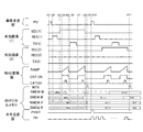
図4は、図1の固体撮像装置1000のモード切り替え時の駆動方法を示すタイミングチャートである。図4では、簡単化のために、4行の非有効画素101と6行の有効画素100の例を図示しているが、実際はより多くの行及び列の画素が配列される。   FIG. 4 is a timing chart showing a driving method at the time of mode switching of the solid-state imaging device 1000 of FIG. In FIG. 4, for the sake of simplicity, an example of four rows of ineffective pixels 101 and six rows of effective pixels 100 is illustrated, but actually, more rows and columns of pixels are arranged.

時刻t40では、読み出し動作を停止する。垂直走査部16、列回路12、列AD変換部13、水平走査部15、信号処理部18、送信部19の動作を停止する。時刻t41以降は、モードを切り替えた後の動作再開シーケンスを示している。   At time t40, the reading operation is stopped. The operations of the vertical scanning unit 16, the column circuit 12, the column AD conversion unit 13, the horizontal scanning unit 15, the signal processing unit 18, and the transmission unit 19 are stopped. After time t41, an operation restart sequence after the mode is switched is shown.

時刻t41では、トレーニングシーケンス生成部182のトレーニングシーケンス生成動作がオンになり、送信部19の出力が開始することにより、送信部19からトレーニングシーケンスデータが出力される。   At time t41, the training sequence generation operation of the training sequence generation unit 182 is turned on, and output of the transmission unit 19 is started, whereby training sequence data is output from the transmission unit 19.

時刻t42では、垂直走査部16及び列AD変換部13は動作を開始する。垂直走査部13は、非有効画素101の1行目を選択する。時刻t42から時刻t43までの期間では、列AD変換部13は、非有効画素101の1行目の信号に対してアナログデジタル変換を行う。列デジタルメモリ14は、アナログデジタル変換後のデジタル値N(1)及びS(1)を書き込みレジスタNMEM_W及びSMEM_Wに格納する。図4で、四角内に1と表しているのは、1行目のデジタル値N(1)及びS(1)を表している。具体的な読み出し期間は、図3の時刻t31から時刻t38までの期間である。水平走査部15はオフのままなので、画素信号処理部181の入力データは無効データのままである。   At time t42, the vertical scanning unit 16 and the column AD conversion unit 13 start operation. The vertical scanning unit 13 selects the first row of the ineffective pixels 101. In the period from time t42 to time t43, the column AD conversion unit 13 performs analog-digital conversion on the signal in the first row of the ineffective pixels 101. The column digital memory 14 stores the digital values N (1) and S (1) after analog-digital conversion in the write registers NMEM_W and SMEM_W. In FIG. 4, “1” in the square represents the digital values N (1) and S (1) in the first row. A specific reading period is a period from time t31 to time t38 in FIG. Since the horizontal scanning unit 15 remains off, the input data of the pixel signal processing unit 181 remains invalid data.

時刻t43から時刻t44までの期間では、非有効画素101の2行目の信号を読み出す。読み出し動作は、図3の時刻t31から時刻t38までの期間と同一の動作である。時刻t44では、列デジタルメモリ14は1列分しかないので、1行目のデジタル値N(1)及びS(1)は上書きされて、2行目のデジタル値N(2)及びS(2)が残る。時刻t44以降では、非有効画素101の3行目以降の信号が巡回して読み出される。   In the period from time t43 to time t44, the signal of the second row of the ineffective pixels 101 is read out. The read operation is the same operation as the period from time t31 to time t38 in FIG. At time t44, since the column digital memory 14 has only one column, the digital values N (1) and S (1) in the first row are overwritten, and the digital values N (2) and S (2) in the second row are overwritten. ) Remains. After time t44, signals from the third row onward of the ineffective pixels 101 are read out in a cyclic manner.

時刻t45から時刻t47までの期間では、トレーニングシーケンス動作から画素出力動作への切り替えを行う。時刻t45では、非有効画素101の1行目の信号の読み出し動作を開始する。非有効画素101の1行目の信号の読み出し中の時刻t46では、信号処理装置の受信部でのクロック復元が完了し、画素信号を受信する準備ができた段階で、信号処理装置の受信部は制御部17に有効画素を読み出す通知を行う。制御部17は、時刻t46時点で、非有効画素101の1行目の信号のアナログデジタル変換が終わっている場合は、時刻t46から時刻t47までの期間に、非有効画素101の1行目のデジタル値N(1)及びS(1)の水平走査動作を開始する。すると、水平走査部15は、列デジタルメモリ14の1行目のデジタル値N(1)及びS(1)を信号処理部18に出力させる。時刻t46で非有効画素101の1行目の信号のアナログデジタル変換が終了していない場合には、非有効画素101の1行目の信号のアナログデジタル変換が完了してから、非有効画素101の1行目のデジタル値N(1)及びS(1)の水平走査動作を開始する。   In a period from time t45 to time t47, switching from the training sequence operation to the pixel output operation is performed. At time t <b> 45, the signal readout operation for the first row of the ineffective pixels 101 is started. At time t46 during reading of the signal of the first row of the non-valid pixel 101, when the clock recovery at the receiving unit of the signal processing device is completed and the pixel signal is ready to be received, the receiving unit of the signal processing device Notifies the control unit 17 to read out effective pixels. When the analog-digital conversion of the signal of the first row of the ineffective pixel 101 is completed at time t46, the control unit 17 performs the first row of the ineffective pixel 101 during the period from time t46 to time t47. The horizontal scanning operation of the digital values N (1) and S (1) is started. Then, the horizontal scanning unit 15 causes the signal processing unit 18 to output the digital values N (1) and S (1) in the first row of the column digital memory 14. If the analog-digital conversion of the signal in the first row of the ineffective pixel 101 is not completed at time t46, the analog-digital conversion of the signal in the first row of the ineffective pixel 101 is completed, and then the ineffective pixel 101 is completed. The horizontal scanning operation of the digital values N (1) and S (1) in the first row is started.

時刻t47では、非有効画素の2行目の信号の読み出しが開始し、トレーニングシーケンス生成部182は、トレーニングシーケンス生成動作をオフし、列デジタルメモリ14から画素信号処理部181にデータが出力される。さらに、制御部17は、信号処理部18内の選択部183を、トレーニングシーケンス生成部182の出力信号の選択を終了し、画素信号処理部181の出力信号の選択を開始する。これにより、送信部19の出力信号は、トレーニングシーケンスから画素出力信号に切り替わる。列デジタルメモリ14は、切り替え前にアナログデジタル変換を行った際の1行目のデジタル値N(1)及びS(1)を保持しているので、トレーニングシーケンス終了後から待機期間をおくことなく、送信部19は画素出力信号を出力することが可能となる。   At time t47, readout of the second row signal of ineffective pixels starts, the training sequence generation unit 182 turns off the training sequence generation operation, and data is output from the column digital memory 14 to the pixel signal processing unit 181. . Further, the control unit 17 ends the selection of the output signal of the training sequence generation unit 182 for the selection unit 183 in the signal processing unit 18 and starts the selection of the output signal of the pixel signal processing unit 181. Thereby, the output signal of the transmission part 19 switches from a training sequence to a pixel output signal. Since the column digital memory 14 holds the digital values N (1) and S (1) in the first row when analog-digital conversion is performed before switching, there is no waiting period after the end of the training sequence. The transmission unit 19 can output a pixel output signal.

以上のように、送信部19は、時刻t41〜t47でトレーニングシーケンスデータ(テスト信号)を送信し、その後の時刻t47以降で列AD変換部13により変換されたデジタル値に基づくデジタル信号を送信する。列AD変換部13は、送信部19がトレーニングシーケンスデータを送信している時刻t42〜tt47の期間に、アナログ信号をデジタル値に変換する。これにより、送信部19は、トレーニングシーケンスデータの送信を終了した後、列AD変換部13により変換されたデジタル値に基づくデジタル信号をすぐに送信することができる。   As described above, the transmission unit 19 transmits the training sequence data (test signal) at time t41 to t47, and transmits a digital signal based on the digital value converted by the column AD conversion unit 13 after time t47. . The column AD conversion unit 13 converts the analog signal into a digital value during a period from time t42 to tt47 when the transmission unit 19 transmits the training sequence data. Thereby, the transmission unit 19 can immediately transmit a digital signal based on the digital value converted by the column AD conversion unit 13 after completing the transmission of the training sequence data.

送信部19は、時刻t46で信号処理装置の受信部からクロック復元完了通知(テスト完了通知)を入力すると、時刻t47で、トレーニングシーケンスデータの送信を終了し、列AD変換部13により変換されたデジタル値に基づくデジタル信号の送信を開始する。画素領域10内の非有効画素101は、送信部19がトレーニングシーケンスデータを送信している時刻t42〜t47の期間に、列回路12を介して列AD変換部13にアナログ信号を出力する。画素領域10内の非有効画素101は、送信部19がトレーニングシーケンスデータの送信を開始した時刻t41の後に、時刻t42で、列回路12を介して列AD変換部13にアナログ信号の出力を開始する。   When the transmission unit 19 inputs a clock restoration completion notification (test completion notification) from the reception unit of the signal processing device at time t46, the transmission unit 19 ends transmission of the training sequence data at time t47 and is converted by the column AD conversion unit 13. Start transmitting a digital signal based on the digital value. The ineffective pixel 101 in the pixel region 10 outputs an analog signal to the column AD conversion unit 13 via the column circuit 12 during a period from time t42 to t47 when the transmission unit 19 transmits the training sequence data. The ineffective pixel 101 in the pixel area 10 starts outputting an analog signal to the column AD conversion unit 13 via the column circuit 12 at time t42 after time t41 when the transmission unit 19 starts transmission of training sequence data. To do.

画素領域10は、各々がアナログ信号を出力する行列状に配列された複数の画素100及び101を有する。垂直走査部16の制御により、複数の画素100及び101は、行単位で順に、列回路12を介して列AD変換部13にアナログ信号を出力する。また、画素領域10は、光電変換部1001を含む有効画素100の行及び光電変換部1001を含まない非有効画素101の行を有する。非有効画素101の行は、送信部19がトレーニングシーケンスデータを送信している時刻t42〜t47の期間に、列回路12を介して列AD変換部13にアナログ信号を出力する。   The pixel area 10 includes a plurality of pixels 100 and 101 arranged in a matrix that each outputs an analog signal. Under the control of the vertical scanning unit 16, the plurality of pixels 100 and 101 sequentially output analog signals to the column AD conversion unit 13 via the column circuit 12 in units of rows. The pixel region 10 includes a row of effective pixels 100 including the photoelectric conversion unit 1001 and a row of non-effective pixels 101 not including the photoelectric conversion unit 1001. The row of the ineffective pixels 101 outputs an analog signal to the column AD conversion unit 13 via the column circuit 12 during a period from time t42 to t47 when the transmission unit 19 transmits training sequence data.

8b10b変換部184は、トレーニングシーケンスデータ又は列AD変換部13により変換されたデジタル値に基づくデジタル信号に対して8b10b変換を行う。送信部19は、時刻t41〜t47で上記の8b10b変換されたトレーニングシーケンスデータを送信し、その後の時刻t47以降で上記の8b10b変換されたデジタル信号を送信する。   The 8b10b conversion unit 184 performs 8b10b conversion on the digital signal based on the training sequence data or the digital value converted by the column AD conversion unit 13. The transmission unit 19 transmits the training sequence data subjected to the 8b10b conversion at time t41 to t47, and transmits the digital signal subjected to the 8b10b conversion after time t47.

図5は、図4の時刻t45から時刻t47までの期間における各回路の動作タイミングを詳細に示すタイミングチャートである。時刻t50では、非有効画素101の1行目の信号の読み出しが開始する。時刻t51では、信号処理装置の受信部は、クロック復元通知を制御部17に出力する。時刻t51では、列デジタルメモリ14内の読み出しメモリNMEM_R及びSMEM_Rには、前行のデジタル値N(4)及びS(4)が書き込まれているため、すぐに水平走査動作を開始することができない。   FIG. 5 is a timing chart showing in detail the operation timing of each circuit in the period from time t45 to time t47 in FIG. At time t50, reading of the first row signal of the ineffective pixel 101 is started. At time t <b> 51, the receiving unit of the signal processing device outputs a clock restoration notification to the control unit 17. At time t51, since the digital values N (4) and S (4) of the previous row are written in the read memories NMEM_R and SMEM_R in the column digital memory 14, the horizontal scanning operation cannot be started immediately. .

時刻t52では、制御部17は、列デジタルメモリ14の信号MTXをハイレベルにして、列デジタルメモリ14内の読み出しメモリNMEM_R及びSMEM_Rに、非有効画素101の1行目のデジタル値N(1)及びS(1)を書き込む。時刻t53では、制御部17は、水平走査部15の信号PHSTをハイレベルにする。すると、水平走査部15は、各列の信号PHを順にハイレベルにすることで、列デジタルメモリ14内の読み出しメモリNMEM_R及びSMEM_Rから信号処理部18にデジタル値N(1)及びS(1)が出力される。画素信号処理部181は、CDS処理により、デジタル値S(1)からデジタル値N(1)を減算した値S(1)−N(1)を出力する。画素信号処理部181の処理にはレイテンシがあるため、時刻t54で、送信部19は、トレーニングシーケンス送信を終了するとともに、画素出力信号S(1)−N(1)の送信を開始する。   At time t <b> 52, the control unit 17 sets the signal MTX of the column digital memory 14 to a high level and stores the digital value N (1) of the first row of the ineffective pixels 101 in the read memories NMEM_R and SMEM_R in the column digital memory 14. And S (1). At time t53, the control unit 17 sets the signal PHST of the horizontal scanning unit 15 to a high level. Then, the horizontal scanning unit 15 sequentially sets the signal PH of each column to the high level, so that the digital values N (1) and S (1) are transferred from the read memories NMEM_R and SMEM_R in the column digital memory 14 to the signal processing unit 18. Is output. The pixel signal processing unit 181 outputs a value S (1) -N (1) obtained by subtracting the digital value N (1) from the digital value S (1) by CDS processing. Since there is latency in the processing of the pixel signal processing unit 181, at time t54, the transmission unit 19 ends transmission of the training sequence and starts transmission of the pixel output signals S (1) -N (1).

クロック復元通知を入力してから垂直走査を開始した場合は、トレーニングシーケンス終了から画素出力信号の出力までの待機期間が時刻t50〜時刻t54までかかるのに対し、本実施形態では、時刻t51からt53までの期間に短縮することが可能となる。   When the vertical scanning is started after the clock restoration notification is input, the waiting period from the end of the training sequence to the output of the pixel output signal is from time t50 to time t54, whereas in the present embodiment, from time t51 to time t53. It becomes possible to shorten to the period until.

クロック復元通知が、ある行の読み出し動作の開始から近い場合には、図5の読み出し動作では、待機期間の低減効果は小さくなる。そこで、別の読み出し方法も実施形態として適用される。   When the clock restoration notification is close to the start of the read operation for a certain row, the read operation of FIG. Therefore, another reading method is also applied as an embodiment.

図6は、トレーニングシーケンスから画素出力信号への切り替えタイミングの別の例を示すタイミングチャートである。時刻t60では、非有効画素101の2行目の信号の読み出しを開始する例である。時刻t61では、制御部17は、水平走査部15の信号PHSTをハイレベルにする。すると、水平走査部15は、各列の信号PHを順にハイレベルにして、列デジタルメモリ14内の読み出しメモリNMEM_R及びSMEM_Rから信号処理部18へ、非有効画素101の1行目のデジタル値N(1)及びS(1)が出力される。画素信号処理部181は、CDS処理により、デジタル値S(1)からデジタル値N(1)を減算した値S(1)−N(1)を出力する。画素信号処理部181の処理にはレイテンシがあるため、時刻t62では、送信部19は、トレーニングシーケンス送信を終了するとともに、画素出力信号S(1)−N(1)の送信を開始する。   FIG. 6 is a timing chart showing another example of the switching timing from the training sequence to the pixel output signal. This is an example in which reading of the signal of the second row of the ineffective pixel 101 is started at time t60. At time t61, the control unit 17 sets the signal PHST of the horizontal scanning unit 15 to a high level. Then, the horizontal scanning unit 15 sequentially sets the signal PH of each column to the high level, and the digital value N of the first row of the ineffective pixels 101 is transferred from the read memories NMEM_R and SMEM_R in the column digital memory 14 to the signal processing unit 18. (1) and S (1) are output. The pixel signal processing unit 181 outputs a value S (1) -N (1) obtained by subtracting the digital value N (1) from the digital value S (1) by CDS processing. Since there is latency in the processing of the pixel signal processing unit 181, at time t62, the transmission unit 19 ends transmission of the training sequence and starts transmission of the pixel output signals S (1) -N (1).

時刻t63は、通常の1行読み出し(図5)時の列デジタルメモリ14の信号MTXをハイレベルにするタイミングである。しかし、通常の1行読み出し(図5)のタイミングと比較して、水平走査部15の読み出し開始時刻t61が画素読み出し開始時刻t60より遅れている。そのため、信号MTXをハイレベルにすると、水平走査部15が読み出している読み出しメモリNMEM_R及びSMEM_Rのデジタル値N(1)及びS(1)を上書きしてしまう。したがって、時刻t63では、制御部17は、信号MTXをハイレベルにせず、1行目のデジタル値N(1)及びS(1)の水平走査が完了する時刻t64で信号MTXをハイレベルにする。   Time t63 is a timing at which the signal MTX of the column digital memory 14 is set to the high level during normal one-row reading (FIG. 5). However, the read start time t61 of the horizontal scanning unit 15 is delayed from the pixel read start time t60 as compared with the timing of normal one-line reading (FIG. 5). Therefore, when the signal MTX is set to the high level, the digital values N (1) and S (1) of the read memories NMEM_R and SMEM_R read by the horizontal scanning unit 15 are overwritten. Therefore, at time t63, the control unit 17 does not set the signal MTX to high level, but sets the signal MTX to high level at time t64 when the horizontal scanning of the digital values N (1) and S (1) in the first row is completed. .

時刻t65では、制御部17は、水平走査部15をリセットし、水平走査部15の信号PHSTをハイレベルにする。すると、水平走査部15は、各列の信号PHを順にハイレベルにし、非有効画素101の2行目のデジタル値N(2)及びS(2)を、読み出しメモリNMEM_R及びSMEM_Rから信号処理部18へ出力させる。   At time t65, the control unit 17 resets the horizontal scanning unit 15 and sets the signal PHST of the horizontal scanning unit 15 to a high level. Then, the horizontal scanning unit 15 sequentially sets the signal PH of each column to the high level, and the digital values N (2) and S (2) of the second row of the ineffective pixels 101 are read from the read memories NMEM_R and SMEM_R. 18 to output.

クロック復元通知が入力された際の行読み出しのタイミングを変更する必要はあるが、クロック復元通知が入力されてから垂直走査を開始した場合は、トレーニングシーケンス終了から画素出力信号の出力までの待機期間が時刻t60から時刻t65までかかる。これに対し、本実施形態では、時刻t61から時刻t62までの期間に短縮することが可能となる。   Although it is necessary to change the row readout timing when the clock recovery notification is input, if the vertical scan starts after the clock recovery notification is input, the waiting period from the end of the training sequence to the output of the pixel output signal Takes from time t60 to time t65. On the other hand, in this embodiment, it is possible to shorten the period from time t61 to time t62.

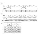
図7(a)〜(c)は、トレーニングシーケンス生成部182が出力するトレーニングシーケンスデータを例示する図である。トレーニングシーケンス生成部182の出力データは、信号処理装置の受信部でクロック復元できるように送受信のプロトコルで規定されている。図7(a)は、トレーニングシーケンス生成部182が出力する8b10b変換前の8ビットデータで示している。K28.5は、Kコードと呼ばれる8b10b変換の規格で規定されるコードである。図7(c)の2列目に書かれている「10111100」が実際の8ビットコードである。トレーニングシーケンス生成部182は、この8ビットデータとKコードであることを示すKフラグをハイレベルにして8b10b変換部184に送信する。すると、8b10b変換部184は、上記の8ビットデータを図7(c)の3列目に示される10ビットコードに変換する。図7(c)のRD−とRD+は、8b10b変換部184の10ビット変換結果が2種類あることを示している。RD−とRD+のどちらになるかはランニングディスパリティと呼ばれる前データの変換結果により決まる符号で決まる。ランニングディスパリティは、前変換データの10ビットに含まれる0と1の個数が同数である場合には前の符号のままで、0と1の個数が異なる場合には、ランニングディスパリティのハイレベルとローレベルを切り替える。こうすることで、連続する0と1が6個以上にならない。   FIGS. 7A to 7C are diagrams illustrating training sequence data output from the training sequence generation unit 182. FIG. The output data of the training sequence generator 182 is defined by a transmission / reception protocol so that the clock can be recovered by the receiver of the signal processing device. FIG. 7A shows 8-bit data before 8b10b conversion output from the training sequence generation unit 182. K28.5 is a code defined by the 8b10b conversion standard called K code. “10111100” written in the second column of FIG. 7C is an actual 8-bit code. The training sequence generation unit 182 sets the K flag indicating the 8-bit data and the K code to a high level, and transmits it to the 8b10b conversion unit 184. Then, the 8b10b conversion unit 184 converts the above 8-bit data into a 10-bit code shown in the third column of FIG. RD− and RD + in FIG. 7C indicate that there are two types of 10-bit conversion results of the 8b10b conversion unit 184. Whether it becomes RD- or RD + is determined by a code determined by the conversion result of the previous data called running disparity. The running disparity is the same as the previous code when the number of 0's and 1's included in 10 bits of the previous conversion data is the same, and the running disparity is at a high level when the number of 0's and 1's is different. And switch the low level. By doing so, the consecutive 0s and 1s do not become 6 or more.

図7(a)において、次のクロック信号CLKでは、トレーニングシーケンス生成部182は、D10.2コードを出力する。D10.2コードは、図7(c)の2列目に示す8ビットコードである。これはKコードではないため、Kフラグはローレベルである。以降、トレーニングシーケンス生成部182は、クロック信号CLKに同期して、D10.2コード及びD10.2コードを順に出力する。トレーニングシーケンス生成部182は、クロック信号CLKの4個のパルスを1単位として繰り返し出力する。   In FIG. 7A, in the next clock signal CLK, the training sequence generation unit 182 outputs the D10.2 code. The D10.2 code is an 8-bit code shown in the second column of FIG. Since this is not a K code, the K flag is at a low level. Thereafter, the training sequence generation unit 182 sequentially outputs the D10.2 code and the D10.2 code in synchronization with the clock signal CLK. The training sequence generation unit 182 repeatedly outputs four pulses of the clock signal CLK as one unit.

図7(b)は、トレーニングシーケンス生成部182が出力するデータの別の例を示している。トレーニングシーケンス生成部182は、クロック信号CLKの4個のパルスに同期して、K28.5コード、K28.0コード、K28.0コード、K28.0コードを出力する。トレーニングシーケンス生成部182は、この単位を1単位として繰り返し出力する。K28.5コード及びK28.0コードの具体的なコードは、図7(c)の2列目に示している。   FIG. 7B shows another example of data output from the training sequence generation unit 182. The training sequence generator 182 outputs a K28.5 code, a K28.0 code, a K28.0 code, and a K28.0 code in synchronization with the four pulses of the clock signal CLK. The training sequence generation unit 182 repeatedly outputs this unit as one unit. Specific codes of the K28.5 code and the K28.0 code are shown in the second column of FIG.

ここで示したトレーニングシーケンスは一例であり、信号処理装置の受信部のプロトコルにより変更されうるので、この限りではない。第1の実施形態において、トレーニングシーケンス送信期間中に読み出す画素は、非有効画素101であることが望ましい。その理由について以下に述べる。トレーニングシーケンスの送信期間は、信号処理装置の受信部がトレーニングシーケンスにより、クロック復元が完了するまでの期間で決まるが、クロック復元が完了する時刻は送受信のインターフェースの状態により前後する不確定性がある。したがって、トレーニングシーケンス終了前にデジタル値を列デジタルメモリ14に格納するためには、垂直走査部16による画素選択及び出力動作をトレーニングシーケンスの時間の不確定性を加味して開始する必要がある。トレーニングシーケンス終了に読み出し1行分以上の時間がかかった場合、1行目の画素の信号は送信部19に読み出せないままとなる。有効画素100の場合、光電変換部1001の電荷を破壊して読み出すので1行目の画素の信号は完全に無効となるが、非有効画素101の場合、光電変換部1001が存在せず非破壊読み出しとなるため、再度の読み出しが可能である。したがって、トレーニングシーケンス送信期間中に読み出す画素は、非有効画素101であることが望ましい。   The training sequence shown here is only an example, and can be changed according to the protocol of the receiving unit of the signal processing apparatus. In the first embodiment, it is desirable that the pixel to be read during the training sequence transmission period is the ineffective pixel 101. The reason will be described below. The transmission period of the training sequence is determined by the period until the clock recovery is completed by the receiving unit of the signal processing device according to the training sequence. However, the time at which the clock recovery is completed is uncertain depending on the state of the transmission / reception interface. . Therefore, in order to store digital values in the column digital memory 14 before the end of the training sequence, it is necessary to start pixel selection and output operations by the vertical scanning unit 16 in consideration of the uncertainty of the training sequence time. When it takes time for one row or more to read out at the end of the training sequence, the signal of the pixel in the first row remains unreadable to the transmitter 19. In the case of the effective pixel 100, the charge of the photoelectric conversion unit 1001 is destroyed and read, so that the signal of the pixel in the first row becomes completely invalid. However, in the case of the non-effective pixel 101, the photoelectric conversion unit 1001 does not exist and is non-destructive. Since reading is performed, reading can be performed again. Therefore, it is desirable that the pixel to be read during the training sequence transmission period is the ineffective pixel 101.

図4において、時刻t40で、画素の読み出し動作を停止し、垂直走査部16、列回路12、列AD変換部13、水平走査部15、信号処理部18及び送信部19の動作を停止するとしたが、これに限定されない。時刻t40の後に時間を空けずに、時刻t41でトレーニングシーケンス生成動作をオンしてもよい。つまり、時刻t40と時刻t41は同時であっても構わない。この場合が本実施形態での最速の動作となる。   In FIG. 4, at the time t40, the pixel reading operation is stopped, and the operations of the vertical scanning unit 16, the column circuit 12, the column AD conversion unit 13, the horizontal scanning unit 15, the signal processing unit 18, and the transmission unit 19 are stopped. However, it is not limited to this. The training sequence generation operation may be turned on at time t41 without leaving time after time t40. That is, time t40 and time t41 may be simultaneous. This is the fastest operation in this embodiment.

図8は、図1の固体撮像装置1000の長秒蓄積時のタイミングチャートである。図4では、簡単化のために、4行の非有効画素101及び6行の有効画素100の場合を図示しているが、実際はより多くの行及び列の画素が配列される。時刻t80では、シャッタ動作を停止する。時刻t80において、垂直走査部16、列回路12、列AD変換部13、水平走査部15、信号処理部18及び送信部19の動作は停止した状態である。時刻t81以降が読み出しのシーケンスを示している。時刻t81では、トレーニングシーケンス生成部182のトレーニングシーケンス生成動作をオンするとともに、送信部19の出力を開始することにより、送信部19からトレーニングシーケンスデータが出力される。   FIG. 8 is a timing chart when the solid-state imaging device 1000 of FIG. In FIG. 4, for simplification, the case of four rows of non-valid pixels 101 and six rows of valid pixels 100 is illustrated, but actually, more rows and columns of pixels are arranged. At time t80, the shutter operation is stopped. At time t80, the operations of the vertical scanning unit 16, the column circuit 12, the column AD conversion unit 13, the horizontal scanning unit 15, the signal processing unit 18, and the transmission unit 19 are stopped. The sequence after time t81 indicates a read sequence. At time t <b> 81, the training sequence generation operation of the training sequence generation unit 182 is turned on and the output of the transmission unit 19 is started, whereby training sequence data is output from the transmission unit 19.

時刻t82では、垂直走査部16及び列AD変換部13の動作を開始する。垂直走査部16は、非有効画素101の1行目を選択する。時刻t82から時刻t83までの期間では、非有効画素101の1行目の信号を読み出し、列AD変換部13はその1行目の信号に対してアナログデジタル変換を行う。アナログデジタル変換後のデジタル値N(1)及びS(1)は、列デジタルメモリ14内の書き込みメモリNMEM_W及びSMEM_Wを書き込まれる。図8の四角内に1と表しているのは、1行目の画素のデジタル値N(1)及びS(1)を表している。具体的な読み出し動作は、図3の時刻t31から時刻t38までの期間の動作となる。水平走査部15は、オフのままなので、画素信号処理部181の入力データは無効データのままである。   At time t82, the operations of the vertical scanning unit 16 and the column AD conversion unit 13 are started. The vertical scanning unit 16 selects the first row of the ineffective pixels 101. In the period from time t82 to time t83, the signal of the first row of the ineffective pixel 101 is read, and the column AD conversion unit 13 performs analog-digital conversion on the signal of the first row. The digital values N (1) and S (1) after analog-digital conversion are written in the write memories NMEM_W and SMEM_W in the column digital memory 14. 8 represents the digital values N (1) and S (1) of the pixels in the first row. A specific read operation is an operation during a period from time t31 to time t38 in FIG. Since the horizontal scanning unit 15 remains off, the input data of the pixel signal processing unit 181 remains invalid data.

時刻t83から時刻t84までの期間では、非有効画素101の2行目の信号を読み出す。読み出し動作は、図3の時刻t31から時刻t38までの期間と同一の動作である。時刻t84では、列デジタルメモリ14は1列分しかないので、1行目のデジタル値N(1)及びS(1)は上書きされて、2行目のデジタル値N(2)及びS(2)が残る。時刻t84以降では、非有効画素101の3行目以降を巡回して読み出す。   In the period from time t83 to time t84, the signal of the second row of the ineffective pixels 101 is read out. The read operation is the same operation as the period from time t31 to time t38 in FIG. At time t84, since the column digital memory 14 has only one column, the digital values N (1) and S (1) in the first row are overwritten, and the digital values N (2) and S (2) in the second row are overwritten. ) Remains. After time t84, the third and subsequent rows of the ineffective pixels 101 are read and read.

時刻t85から時刻t87において、トレーニングシーケンスから画素出力動作への切り替えを行う。時刻t85では、非有効画素101の1行目の信号の読み出し動作を開始する。非有効画素101の1行目の信号の読み出し中の時刻t86では、信号処理装置の受信部は、クロック復元を完了し、画素信号を受信する準備ができた段階で、制御部17に有効画素100を読み出す通知を行う。制御部17は、時刻t86時点で、非有効画素101の1行目の信号のアナログデジタル変換が終わっている場合は、時刻t86から時刻t87までの間の期間に、水平走査部15は水平走査動作を開始する。時刻t86時点で非有効画素101の1行目の信号のアナログデジタル変換が終了していない場合には、非有効画素101の1行目の信号のアナログデジタル変換が完了してから、水平走査部15は水平走査動作を開始する。   From time t85 to time t87, switching from the training sequence to the pixel output operation is performed. At time t85, the signal readout operation for the first row of the ineffective pixels 101 is started. At time t86 during reading of the signal of the first row of the non-valid pixel 101, the receiving unit of the signal processing device completes the clock restoration and is ready to receive the pixel signal. Notification to read 100 is performed. When the analog-digital conversion of the signal in the first row of the ineffective pixel 101 is completed at time t86, the control unit 17 performs horizontal scanning in the period from time t86 to time t87. Start operation. When the analog-digital conversion of the first row signal of the ineffective pixel 101 is not completed at time t86, the horizontal scanning unit after the analog-digital conversion of the first row signal of the ineffective pixel 101 is completed. 15 starts a horizontal scanning operation.

時刻t87では、非有効画素101の2行目の信号の読み出しを開始し、トレーニングシーケンス生成部182はトレーニングシーケンス生成動作をオフし、列デジタルメモリ14から画素信号処理部181にデジタル値N(1)及びS(1)を出力する。さらに、制御部17の制御により、信号処理部18内の選択部183は、トレーニングシーケンス生成部182の出力信号の出力を終了し、画素信号処理部181の出力信号の出力を開始する。すると、送信部19の出力信号は、トレーニングシーケンスデータから画素出力信号に切り替えられる。列デジタルメモリ14は、切り替え前にアナログデジタル変換を行った際の1行目のデジタル値N(1)及びS(1)を保持しているので、トレーニングシーケンス終了後から待機期間をおくことなく、送信部19は画素出力信号を出力することが可能となる。時刻t85〜t87の期間の読み出し動作は、図5の時刻t50〜t57の期間の読み出し動作と同じである。信号処理装置の受信部のクロック復元のタイミングによっては、時刻t85〜t87の期間の読み出し方法は、図6の時刻t60〜t65の読み出し方法でもよい。これにより、長秒蓄積開始から読み出し開始までの待機期間を短縮することが可能となる。   At time t87, reading of the signal of the second row of the ineffective pixel 101 is started, the training sequence generation unit 182 turns off the training sequence generation operation, and the digital value N (1) is transferred from the column digital memory 14 to the pixel signal processing unit 181. ) And S (1). Further, under the control of the control unit 17, the selection unit 183 in the signal processing unit 18 finishes outputting the output signal of the training sequence generation unit 182 and starts outputting the output signal of the pixel signal processing unit 181. Then, the output signal of the transmission unit 19 is switched from the training sequence data to the pixel output signal. Since the column digital memory 14 holds the digital values N (1) and S (1) in the first row when analog-digital conversion is performed before switching, there is no waiting period after the end of the training sequence. The transmission unit 19 can output a pixel output signal. The read operation during the period from time t85 to t87 is the same as the read operation during the period from time t50 to t57 in FIG. Depending on the timing of clock recovery of the receiving unit of the signal processing device, the reading method during the period from time t85 to t87 may be the reading method from time t60 to t65 in FIG. Thereby, it is possible to shorten the waiting period from the start of long-second accumulation to the start of reading.

(第2の実施形態)
本発明の第2の実施形態による固体撮像装置1000の構成は、第1の実施形態の図1と同じであり、画素領域10の構成も第1の実施形態の図2と同じである。
(Second Embodiment)
The configuration of the solid-state imaging device 1000 according to the second embodiment of the present invention is the same as that of FIG. 1 of the first embodiment, and the configuration of the pixel region 10 is also the same as that of FIG. 2 of the first embodiment.

図9は、本発明の第2の実施形態による固体撮像装置1000の長秒蓄積時のタイミングチャートである。図9では、簡単化のために、4行の非有効画素101及び6行の有効画素100の場合を図示しているが、実際はより多くの行及び列の画素が配列される。時刻t90では、シャッタ動作を停止する。時刻t90において、垂直走査部16、列回路12、列AD変換部13、水平走査部15、信号処理部18及び送信部19の動作は停止した状態である。時刻t91以降が読み出しのシーケンスを示している。時刻t91では、トレーニングシーケンス生成部182は、トレーニングシーケンス生成動作をオンするとともに、送信部19は出力を開始する。これにより、送信部19からトレーニングシーケンスデータが出力される。   FIG. 9 is a timing chart when the solid-state imaging device 1000 according to the second embodiment of the present invention accumulates for a long time. For simplification, FIG. 9 illustrates the case of four rows of non-valid pixels 101 and six rows of valid pixels 100, but in reality, more rows and columns of pixels are arranged. At time t90, the shutter operation is stopped. At time t90, the operations of the vertical scanning unit 16, the column circuit 12, the column AD conversion unit 13, the horizontal scanning unit 15, the signal processing unit 18, and the transmission unit 19 are stopped. The time sequence after time t91 indicates a read sequence. At time t91, the training sequence generation unit 182 turns on the training sequence generation operation, and the transmission unit 19 starts output. Thereby, training sequence data is output from the transmission unit 19.

時刻t92では、垂直走査部16及び列AD変換部13の動作を開始する。垂直走査部16は、非有効画素101の1行目を選択する。時刻t92から時刻t93までの期間では、非有効画素101の1行目の信号を読み出し、列AD変換部13はその1行目の信号に対してアナログデジタル変換を行う。アナログデジタル変換後のデジタル値N(1)及びS(1)は、列デジタルメモリ14内の書き込みメモリNMEM_W及びSMEM_Wに書き込まれる。図9の四角内に1と表しているのは、1行目のデジタル値N(1)及びS(1)を表している。具体的な読み出し動作は、図3の時刻t31から時刻t38までの期間の動作となる。水平走査部15はオフのままなので、画素信号処理部181の入力データは無効データのままである。   At time t92, the operations of the vertical scanning unit 16 and the column AD conversion unit 13 are started. The vertical scanning unit 16 selects the first row of the ineffective pixels 101. In the period from time t92 to time t93, the signal of the first row of the ineffective pixel 101 is read, and the column AD conversion unit 13 performs analog-digital conversion on the signal of the first row. The digital values N (1) and S (1) after analog-digital conversion are written into the write memories NMEM_W and SMEM_W in the column digital memory 14. In the square of FIG. 9, “1” represents the digital values N (1) and S (1) in the first row. A specific read operation is an operation during a period from time t31 to time t38 in FIG. Since the horizontal scanning unit 15 remains off, the input data of the pixel signal processing unit 181 remains invalid data.

時刻t93以降では、垂直走査部16の非有効画素101の走査と列AD変換部13のアナログデジタル変換動作を止める。これにより、画素走査とアナログデジタル変換動作の更なる消費電力低減が可能となる。   After time t93, the scanning of the ineffective pixels 101 of the vertical scanning unit 16 and the analog-digital conversion operation of the column AD conversion unit 13 are stopped. As a result, it is possible to further reduce power consumption in pixel scanning and analog-digital conversion operations.

時刻t94から時刻t95において、トレーニングシーケンスから画素出力動作への切り替えを行う。時刻t94では、信号処理装置の受信部は、クロック復元を完了し、画素信号を受信する準備ができた段階で、制御部17に有効画素100を読み出す通知を行う。制御部17は、時刻t94時点で非有効画素101の1行目の信号のアナログデジタル変換が終わっている場合は、時刻t94から時刻t95までの期間に、水平走査部15は水平走査動作を開始する。時刻t94時点で非有効画素101の1行目の信号のアナログデジタル変換が終了していない場合には、1行目の信号のアナログデジタル変換が完了してから、水平走査部15は水平走査動作を開始する。   From time t94 to time t95, switching from the training sequence to the pixel output operation is performed. At time t94, the receiving unit of the signal processing device notifies the control unit 17 to read out the effective pixel 100 when the clock restoration is completed and the pixel signal is ready to be received. When the analog-digital conversion of the signal of the first row of the ineffective pixel 101 is completed at time t94, the control unit 17 starts the horizontal scanning operation in the period from time t94 to time t95. To do. If the analog-digital conversion of the signal of the first row of the ineffective pixel 101 is not completed at time t94, the horizontal scanning unit 15 performs the horizontal scanning operation after the analog-digital conversion of the signal of the first row is completed. To start.

時刻t95では、非有効画素101の2行目の信号の読み出しを開始し、トレーニングシーケンス生成部182はトレーニングシーケンス生成動作をオフするとともに、列デジタルメモリ14から画素信号処理部181にデータを出力する。さらに、制御部17の制御により、信号処理部18内の選択部183は、トレーニングシーケンス生成部182の出力信号の出力を終了し、画素信号処理部181の出力信号の出力を開始する。これにより、送信部19の出力データは、トレーニングシーケンスデータから画素出力信号に切り替えられる。列デジタルメモリ14は、切り替え前にアナログデジタル変換を行った際の非有効画素101の1行目のデジタル値N(1)及びS(1)を保持している。そのため、トレーニングシーケンス終了後から待機期間をおくことなく、送信部19は画素出力信号を出力することが可能となる。   At time t95, reading of the signal of the second row of the ineffective pixels 101 is started, and the training sequence generation unit 182 turns off the training sequence generation operation and outputs data from the column digital memory 14 to the pixel signal processing unit 181. . Further, under the control of the control unit 17, the selection unit 183 in the signal processing unit 18 finishes outputting the output signal of the training sequence generation unit 182 and starts outputting the output signal of the pixel signal processing unit 181. Thereby, the output data of the transmission part 19 is switched from training sequence data to a pixel output signal. The column digital memory 14 holds the digital values N (1) and S (1) of the first row of the ineffective pixels 101 when analog-digital conversion is performed before switching. Therefore, the transmission unit 19 can output the pixel output signal without waiting for the training sequence to end.

時刻t94〜t95の読み出し動作は、図5の時刻t50〜t57の読み出し動作と同じである。信号処理装置の受信部のクロック復元のタイミングによっては、時刻t94〜t95の読み出し動作は、図6の時刻t60〜t65の読み出し動作でもよい。これにより、長秒蓄積開始から読み出し開始までの待機期間を短縮することが可能となる。また、トレーニングシーケンス送信時に列AD変換部13のアナログデジタル変換動作を止めるため、消費電力低減も可能となる。   The read operation from time t94 to t95 is the same as the read operation from time t50 to t57 in FIG. Depending on the timing of clock recovery of the receiving unit of the signal processing device, the read operation from time t94 to t95 may be the read operation from time t60 to t65 in FIG. Thereby, it is possible to shorten the waiting period from the start of long-second accumulation to the start of reading. Further, since the analog-digital conversion operation of the column AD conversion unit 13 is stopped when the training sequence is transmitted, power consumption can be reduced.

以上のように、列AD変換部13は、送信部19がトレーニングシーケンスデータを送信している時刻t92〜t93の期間に、1行の非有効画素101が出力したアナログ信号をデジタル値に変換した後に変換動作を停止する。その後、列AD変換部13は、送信部19が列AD変換部13により変換されたデジタル値に基づくデジタル信号の送信を開始する際に、時刻t95で変換動作を再開する。   As described above, the column AD conversion unit 13 converts the analog signal output from one row of ineffective pixels 101 into a digital value during the period from time t92 to t93 when the transmission unit 19 transmits the training sequence data. The conversion operation is stopped later. Thereafter, the column AD conversion unit 13 resumes the conversion operation at time t95 when the transmission unit 19 starts transmitting a digital signal based on the digital value converted by the column AD conversion unit 13.

第1及び第2の実施形態によれば、撮像モード切り替え時や長秒蓄積駆動時の有効画素出力までの待機期間を短縮することができる。   According to the first and second embodiments, it is possible to shorten the waiting period until the effective pixel output at the time of switching the imaging mode or at the time of long-second accumulation driving.

(第3の実施形態)
上記の各実施形態で述べた固体撮像装置は、種々の撮像システムに適用可能である。撮像システムの一例としては、デジタルスチルカメラ、デジタルカムコーダー、監視カメラなどがあげられる。図10に、撮像システムの一例としてデジタルスチルカメラに、上述した実施形態のいずれかの固体撮像装置1000を適用した撮像システムの図を示す。図10の固体撮像装置154は、上記の固体撮像装置1000に対応する。図10に例示した撮像システムは、固体撮像装置154、レンズ152の保護のためのバリア151、被写体の光学像を固体撮像装置154に結像させるレンズ152、及びレンズ152を通過する光量を可変にするための絞り153を有する。レンズ152及び絞り153は固体撮像装置154に光を集光する光学系である。また、図10に例示した撮像システムは、固体撮像装置154の送信部19より出力される出力信号の処理を行う出力信号処理部155を有する。出力信号処理部155は、固体撮像装置154の送信部19が出力するデジタル信号に基づいて画像を生成する。具体的には、出力信号処理部155は、その他、必要に応じて、各種の補正及び圧縮を行って、画像データを出力する。
(Third embodiment)
The solid-state imaging device described in each of the above embodiments can be applied to various imaging systems. Examples of the imaging system include a digital still camera, a digital camcorder, and a surveillance camera. FIG. 10 shows a diagram of an imaging system in which any one of the above-described solid-state imaging devices 1000 is applied to a digital still camera as an example of the imaging system. A solid-state imaging device 154 in FIG. 10 corresponds to the solid-state imaging device 1000 described above. The imaging system illustrated in FIG. 10 has a solid-state imaging device 154, a barrier 151 for protecting the lens 152, a lens 152 that forms an optical image of a subject on the solid-state imaging device 154, and a light amount that passes through the lens 152 is variable. There is a diaphragm 153 for this purpose. The lens 152 and the diaphragm 153 are an optical system that focuses light on the solid-state imaging device 154. The imaging system illustrated in FIG. 10 includes an output signal processing unit 155 that processes an output signal output from the transmission unit 19 of the solid-state imaging device 154. The output signal processing unit 155 generates an image based on the digital signal output from the transmission unit 19 of the solid-state imaging device 154. Specifically, the output signal processing unit 155 performs various corrections and compressions as necessary, and outputs image data.

図10に例示した撮像システムは、さらに、画像データを一時的に記憶するためのバッファメモリ部156、外部コンピュータ等と通信するための外部インターフェース部(外部I/F部)157を有する。さらに、撮像システムは、撮像データの記録又は読み出しを行うための半導体メモリ等の記録媒体159、記録媒体159に記録又は読み出しを行うための記録媒体制御インターフェース部(記録媒体制御I/F部)158を有する。なお、記録媒体159は、撮像システムに内蔵されていてもよく、着脱可能であってもよい。   The imaging system illustrated in FIG. 10 further includes a buffer memory unit 156 for temporarily storing image data, and an external interface unit (external I / F unit) 157 for communicating with an external computer or the like. Further, the imaging system includes a recording medium 159 such as a semiconductor memory for recording or reading imaging data, and a recording medium control interface unit (recording medium control I / F unit) 158 for recording or reading to the recording medium 159. Have Note that the recording medium 159 may be built in the imaging system or may be detachable.

さらに、撮像システムは、各種演算とデジタルスチルカメラ全体を制御する全体制御・演算部1510、固体撮像装置154と出力信号処理部155に各種タイミング信号を出力するタイミング発生部1511を有する。ここで、タイミング信号などは、外部から入力されてもよく、撮像システムは少なくとも固体撮像装置154と、固体撮像装置154から出力された出力信号を処理する出力信号処理部155とを有すればよい。   Further, the imaging system includes a general control / arithmetic unit 1510 that controls various calculations and the entire digital still camera, and a timing generation unit 1511 that outputs various timing signals to the solid-state imaging device 154 and the output signal processing unit 155. Here, the timing signal or the like may be input from the outside, and the imaging system only needs to include at least the solid-state imaging device 154 and the output signal processing unit 155 that processes the output signal output from the solid-state imaging device 154. .

以上のように、本実施形態の撮像システムは、固体撮像装置154を適用して撮像動作を行うことが可能である。   As described above, the imaging system of the present embodiment can perform an imaging operation by applying the solid-state imaging device 154.

なお、上記実施形態は、何れも本発明を実施するにあたっての具体化の例を示したものに過ぎず、これらによって本発明の技術的範囲が限定的に解釈されてはならないものである。すなわち、本発明はその技術思想、又はその主要な特徴から逸脱することなく、様々な形で実施することができる。   The above-described embodiments are merely examples of implementation in carrying out the present invention, and the technical scope of the present invention should not be construed in a limited manner. That is, the present invention can be implemented in various forms without departing from the technical idea or the main features thereof.

10 画素領域、100 有効画素、101 非有効画素、13 列AD変換部、19 送信部 10 pixel area, 100 effective pixel, 101 non-effective pixel, 13 column AD conversion unit, 19 transmission unit

Claims (17)

アナログ信号を出力する画素領域と、
前記アナログ信号をデジタル信号に変換するアナログデジタル変換部と、
テスト信号を送信し、その後に前記アナログデジタル変換部により変換された前記デジタル信号を送信する送信部とを有し、
前記アナログデジタル変換部は、前記送信部が前記テスト信号を送信している期間に、前記アナログ信号を前記デジタル信号に変換することを特徴とする固体撮像装置。
A pixel region for outputting an analog signal;
An analog-to-digital converter that converts the analog signal into a digital signal;
A transmission unit that transmits a test signal and then transmits the digital signal converted by the analog-digital conversion unit;
The solid-state imaging device, wherein the analog-digital conversion unit converts the analog signal into the digital signal during a period in which the transmission unit transmits the test signal.
前記送信部は、テスト完了通知を入力すると、前記テスト信号の送信を終了し、前記アナログデジタル変換部により変換されたデジタル信号の送信を開始することを特徴とする請求項1記載の固体撮像装置。   2. The solid-state imaging device according to claim 1, wherein when the test completion notification is input, the transmission unit ends transmission of the test signal and starts transmission of the digital signal converted by the analog-digital conversion unit. . 前記画素領域は、前記送信部が前記テスト信号を送信している期間に、前記アナログデジタル変換部に前記アナログ信号を出力することを特徴とする請求項1又は2記載の固体撮像装置。   3. The solid-state imaging device according to claim 1, wherein the pixel region outputs the analog signal to the analog-digital conversion unit during a period in which the transmission unit transmits the test signal. 前記画素領域は、前記送信部が前記テスト信号の送信を開始した後に、前記アナログデジタル変換部に前記アナログ信号の出力を開始することを特徴とする請求項1〜3のいずれか1項に記載の固体撮像装置。   4. The pixel area according to claim 1, wherein after the transmission unit starts transmitting the test signal, the pixel region starts output of the analog signal to the analog-digital conversion unit. 5. Solid-state imaging device. 前記画素領域は、各々がアナログ信号を出力する行列状に配列された複数の画素を有し、
前記複数の画素は、行単位で順に前記アナログデジタル変換部に前記アナログ信号を出力することを特徴とする請求項1〜4のいずれか1項に記載の固体撮像装置。
The pixel region has a plurality of pixels arranged in a matrix each outputting an analog signal,
5. The solid-state imaging device according to claim 1, wherein the plurality of pixels sequentially output the analog signals to the analog-digital conversion unit in units of rows.
前記画素領域は、光電変換部を含む有効画素の行及び光電変換部を含まない非有効画素の行を有し、
前記非有効画素の行は、前記送信部が前記テスト信号を送信している期間に、前記アナログデジタル変換部に前記アナログ信号を出力することを特徴とする請求項5記載の固体撮像装置。
The pixel region has a row of effective pixels including a photoelectric conversion unit and a row of ineffective pixels not including a photoelectric conversion unit,
The solid-state imaging device according to claim 5, wherein the row of the ineffective pixels outputs the analog signal to the analog-to-digital conversion unit during a period in which the transmission unit transmits the test signal.
前記アナログデジタル変換部は、前記送信部が前記テスト信号を送信している期間に、1行の前記画素が出力したアナログ信号をデジタル信号に変換した後に変換動作を停止し、前記送信部が前記アナログデジタル変換部により変換されたデジタル信号の送信を開始する際に、変換動作を再開することを特徴とする請求項5又は6記載の固体撮像装置。   The analog-to-digital conversion unit stops the conversion operation after converting the analog signal output from the pixels in one row into a digital signal during a period in which the transmission unit transmits the test signal, and the transmission unit 7. The solid-state imaging device according to claim 5, wherein the conversion operation is restarted when transmission of the digital signal converted by the analog-digital conversion unit is started. 前記アナログデジタル変換部は、前記送信部が前記テスト信号を送信している期間に、1行の前記非有効画素が出力したアナログ信号をデジタル信号に変換した後に変換動作を停止し、前記送信部が前記アナログデジタル変換部により変換されたデジタル信号の送信を開始する際に、変換動作を再開することを特徴とする請求項6記載の固体撮像装置。   The analog-to-digital conversion unit stops the conversion operation after converting the analog signal output from the invalid pixel in one row into a digital signal during a period in which the transmission unit transmits the test signal, and the transmission unit 7. The solid-state imaging device according to claim 6, wherein the conversion operation is resumed when transmission of the digital signal converted by the analog-digital conversion unit is started. テスト信号又は前記アナログデジタル変換部により変換されたデジタル信号に対して8b10b変換を行う8b10b変換部をさらに有し、
前記送信部は、前記8b10b変換されたテスト信号を送信し、その後に前記8b10b変換されたデジタル信号を送信することを特徴とする請求項1〜8のいずれか1項に記載の固体撮像装置。
Further comprising a 8b10b conversion unit that performs 8b10b conversion for the test signal or the digital signal converted by the analog-digital converter unit,
9. The solid-state imaging device according to claim 1, wherein the transmission unit transmits the 8b10b-converted test signal, and then transmits the 8b10b-converted digital signal. 10.
前記デジタル信号と前記テスト信号の一方を選択して出力する選択部をさらに有することを特徴とする請求項1〜9のいずれか1項に記載の固体撮像装置。The solid-state imaging device according to claim 1, further comprising a selection unit that selects and outputs one of the digital signal and the test signal. 前記選択部は、前記アナログデジタル変換部がアナログ信号をデジタル信号に変換している間は、前記テスト信号を選択し、前記アナログデジタル変換部の変換が終わった後に、前記デジタル信号を選択することを特徴とする請求項10記載の固体撮像装置。The selection unit selects the test signal while the analog-digital conversion unit is converting an analog signal into a digital signal, and selects the digital signal after the conversion of the analog-digital conversion unit is completed. The solid-state imaging device according to claim 10. 前記送信部は、受信部でのクロック復元が完了したことを知らせる信号を受理した後に、前記デジタル信号の送信を開始することを特徴とする請求項1〜11のいずれか1項に記載の固体撮像装置。The solid-state signal according to any one of claims 1 to 11, wherein the transmission unit starts transmission of the digital signal after receiving a signal informing that the clock recovery in the reception unit is completed. Imaging device. 前記アナログデジタル変換部は、メモリを有し、The analog-digital converter has a memory,
前記送信部は、前記アナログデジタル変換部のメモリに保持されているデジタル信号を送信することを特徴とする請求項1〜12のいずれか1項に記載の固体撮像装置。The solid-state imaging device according to claim 1, wherein the transmission unit transmits a digital signal held in a memory of the analog-digital conversion unit.
前記アナログデジタル変換部のメモリは、第1のメモリと第2のメモリを有し、The memory of the analog-digital conversion unit has a first memory and a second memory,
前記アナログデジタル変換部は、アナログ信号からデジタル信号への変換が終わった後に、前記第1のメモリから前記第2のメモリへ前記デジタル信号を転送し、The analog-to-digital conversion unit transfers the digital signal from the first memory to the second memory after the conversion from the analog signal to the digital signal is completed,
前記送信部は、前記第2のメモリに保持されているデジタル信号を送信することを特徴とする請求項13記載の固体撮像装置。The solid-state imaging device according to claim 13, wherein the transmission unit transmits a digital signal held in the second memory.
前記テスト信号は、クロック復元を行うためのデータを含むことを特徴とする請求項1〜14のいずれか1項に記載の固体撮像装置。The solid-state imaging device according to claim 1, wherein the test signal includes data for performing clock recovery. 請求項1〜15のいずれか1項に記載の固体撮像装置と、
前記固体撮像装置の前記送信部から出力される前記デジタル信号に基づいて画像を生成する出力信号処理部とを有することを特徴とする撮像システム。
The solid-state imaging device according to any one of claims 1 to 15 ,
An imaging system comprising: an output signal processing unit that generates an image based on the digital signal output from the transmission unit of the solid-state imaging device.
アナログ信号を出力する画素領域と、
前記アナログ信号をデジタル信号に変換するアナログデジタル変換部とを有する固体撮像装置の駆動方法であって、
送信部により、テスト信号を送信するステップと、
前記アナログデジタル変換部により、前記送信部が前記テスト信号を送信している期間に、前記アナログ信号をデジタル信号に変換するステップと、
前記送信部により、前記テスト信号の送信を終了し、その後に前記アナログデジタル変換部により変換された前記デジタル信号を送信するステップと
を有することを特徴とする固体撮像装置の駆動方法。
A pixel region for outputting an analog signal;
A method of driving a solid-state imaging device having an analog-to-digital converter that converts the analog signal into a digital signal,
Transmitting a test signal by the transmission unit;
Converting the analog signal into a digital signal by the analog-to-digital converter during a period in which the transmitter is transmitting the test signal;
A method of driving the solid-state imaging device, comprising: a step of transmitting the test signal by the transmitting unit and then transmitting the digital signal converted by the analog-to-digital converting unit.
JP2014250278A 2014-12-10 2014-12-10 Solid-state imaging device, imaging system, and driving method of solid-state imaging device Active JP6448340B2 (en)

Priority Applications (2)

Application Number Priority Date Filing Date Title
JP2014250278A JP6448340B2 (en) 2014-12-10 2014-12-10 Solid-state imaging device, imaging system, and driving method of solid-state imaging device
US14/926,125 US9900535B2 (en) 2014-12-10 2015-10-29 Solid-state imaging apparatus, imaging system and method for driving solid-state imaging apparatus

Applications Claiming Priority (1)

Application Number Priority Date Filing Date Title
JP2014250278A JP6448340B2 (en) 2014-12-10 2014-12-10 Solid-state imaging device, imaging system, and driving method of solid-state imaging device

Publications (3)

Publication Number Publication Date
JP2016111656A JP2016111656A (en) 2016-06-20
JP2016111656A5 JP2016111656A5 (en) 2018-01-25
JP6448340B2 true JP6448340B2 (en) 2019-01-09

Family

ID=56112419

Family Applications (1)

Application Number Title Priority Date Filing Date
JP2014250278A Active JP6448340B2 (en) 2014-12-10 2014-12-10 Solid-state imaging device, imaging system, and driving method of solid-state imaging device

Country Status (2)

Country Link
US (1) US9900535B2 (en)
JP (1) JP6448340B2 (en)

Families Citing this family (11)

* Cited by examiner, † Cited by third party
Publication number Priority date Publication date Assignee Title
WO2016117401A1 (en) * 2015-01-20 2016-07-28 日立オートモティブシステムズ株式会社 On-vehicle camera device
JP6628497B2 (en) 2015-05-19 2020-01-08 キヤノン株式会社 Imaging device, imaging system, and image processing method
JP6556001B2 (en) * 2015-09-24 2019-08-07 キヤノン株式会社 Image reading device
JP6436953B2 (en) 2016-09-30 2018-12-12 キヤノン株式会社 Solid-state imaging device, driving method thereof, and imaging system
CN110036632B (en) * 2016-12-08 2021-07-09 新唐科技日本株式会社 Solid-state imaging device and imaging device using the same
JP7075208B2 (en) 2017-12-22 2022-05-25 キヤノン株式会社 Imaging equipment and imaging system
JP7157529B2 (en) 2017-12-25 2022-10-20 キヤノン株式会社 Imaging device, imaging system, and imaging device driving method
JP7260990B2 (en) 2018-10-26 2023-04-19 キヤノン株式会社 Imaging device and imaging system
JP7237622B2 (en) 2019-02-05 2023-03-13 キヤノン株式会社 Photoelectric conversion device
US11368639B2 (en) * 2019-09-30 2022-06-21 Canon Kabushiki Kaisha Photoelectric conversion apparatus, image capturing system, method for driving photoelectric conversion apparatus, and moving object
JP2022051134A (en) 2020-09-18 2022-03-31 キヤノン株式会社 Imaging device and imaging system

Family Cites Families (8)

* Cited by examiner, † Cited by third party
Publication number Priority date Publication date Assignee Title
JP3487768B2 (en) * 1997-10-15 2004-01-19 シャープ株式会社 Signal transmission equipment
US7928884B2 (en) * 2007-01-11 2011-04-19 Siflare, Inc. Analog-to-digital converter with a balanced output
JP5142703B2 (en) * 2007-05-21 2013-02-13 キヤノン株式会社 Imaging apparatus and processing method thereof
JP2011049901A (en) * 2009-08-27 2011-03-10 Panasonic Corp Solid-state imaging unit, and imaging apparatus
JP2011211535A (en) * 2010-03-30 2011-10-20 Sony Corp Solid-state imaging device and camera system
JP2012049912A (en) * 2010-08-27 2012-03-08 Canon Inc Photoelectric conversion device and imaging system
US8970750B2 (en) * 2010-11-12 2015-03-03 Sony Corporation Image outputting apparatus, image outputting method, image processing apparatus, image processing method, program, data structure and imaging apparatus
JP5814050B2 (en) * 2011-09-02 2015-11-17 ルネサスエレクトロニクス株式会社 Solid-state imaging device

Also Published As

Publication number Publication date
JP2016111656A (en) 2016-06-20
US20160173796A1 (en) 2016-06-16
US9900535B2 (en) 2018-02-20

Similar Documents

Publication Publication Date Title
JP6448340B2 (en) Solid-state imaging device, imaging system, and driving method of solid-state imaging device
JP7005501B2 (en) Solid-state image sensor, its driving method, and electronic devices
US9479189B2 (en) A/D converter, solid-state imaging device and camera system
US9237285B2 (en) Solid-state image pickup device and camera system
JP4929075B2 (en) Solid-state imaging device, driving method thereof, and imaging device
US9332202B2 (en) Solid-state imaging apparatus and imaging system
US9658643B2 (en) Data interface and data transmission method
JP5256874B2 (en) Solid-state imaging device and camera system
JP2008141610A (en) Solid-state imaging apparatus, and imaging system
US10707852B2 (en) Comparator, AD converter, solid-state imaging apparatus, electronic apparatus, and method of controlling comparator
US20150124137A1 (en) A/d conversion device, solid-state image-capturing device, and electronic device
JP2010251957A (en) A/d converter, solid-state image sensing device, and camera system
US9083368B2 (en) Image sensor using offset code for counting
US11202023B2 (en) Imaging device and imaging system
KR20160063856A (en) An image sensor, and an image processing system including the image sensor
CN107231534B (en) Pixel output level control device and CMOS image sensor using the same
KR20160015712A (en) Apparatus and method for capturing images
US11146749B2 (en) Image sensor, electronic system including the same, and method of operating the same
JP2016103780A (en) Imaging device, imaging system, and method of driving imaging apparatus
KR102195408B1 (en) Data interface and data transmit method
KR102474575B1 (en) An image sensor, and an image processing system including the image sensor
JP2024021074A (en) Image sensor performing selective multiple sampling and operating method thereof

Legal Events

Date Code Title Description
A521 Request for written amendment filed

Free format text: JAPANESE INTERMEDIATE CODE: A523

Effective date: 20171207

A621 Written request for application examination

Free format text: JAPANESE INTERMEDIATE CODE: A621

Effective date: 20171207

A977 Report on retrieval

Free format text: JAPANESE INTERMEDIATE CODE: A971007

Effective date: 20181010

TRDD Decision of grant or rejection written
A01 Written decision to grant a patent or to grant a registration (utility model)

Free format text: JAPANESE INTERMEDIATE CODE: A01

Effective date: 20181106

A61 First payment of annual fees (during grant procedure)

Free format text: JAPANESE INTERMEDIATE CODE: A61

Effective date: 20181204

R151 Written notification of patent or utility model registration

Ref document number: 6448340

Country of ref document: JP

Free format text: JAPANESE INTERMEDIATE CODE: R151