JP6428675B2 - Light source device for pattern drawing - Google Patents

Light source device for pattern drawing Download PDF

Info

Publication number
JP6428675B2
JP6428675B2 JP2016030856A JP2016030856A JP6428675B2 JP 6428675 B2 JP6428675 B2 JP 6428675B2 JP 2016030856 A JP2016030856 A JP 2016030856A JP 2016030856 A JP2016030856 A JP 2016030856A JP 6428675 B2 JP6428675 B2 JP 6428675B2
Authority
JP
Japan
Prior art keywords
light
light source
unit
source device
laser beam
Prior art date
Legal status (The legal status is an assumption and is not a legal conclusion. Google has not performed a legal analysis and makes no representation as to the accuracy of the status listed.)
Active
Application number
JP2016030856A
Other languages
Japanese (ja)
Other versions
JP2016153893A5 (en
JP2016153893A (en
Inventor
加藤 正紀
正紀 加藤
Current Assignee (The listed assignees may be inaccurate. Google has not performed a legal analysis and makes no representation or warranty as to the accuracy of the list.)
Nikon Corp
Original Assignee
Nikon Corp
Priority date (The priority date is an assumption and is not a legal conclusion. Google has not performed a legal analysis and makes no representation as to the accuracy of the date listed.)
Filing date
Publication date
Application filed by Nikon Corp filed Critical Nikon Corp
Priority to JP2016030856A priority Critical patent/JP6428675B2/en
Publication of JP2016153893A publication Critical patent/JP2016153893A/en
Publication of JP2016153893A5 publication Critical patent/JP2016153893A5/ja
Application granted granted Critical
Publication of JP6428675B2 publication Critical patent/JP6428675B2/en
Active legal-status Critical Current
Anticipated expiration legal-status Critical

Links

Images

Description

本発明は、被照射体上にパターンを露光するためのビームを射出するパターン描画用の光源装置に関する。 The present invention relates to a light source device for pattern drawing that emits a beam for exposing a pattern onto an object to be irradiated.

下記特許文献1に開示されているように、1つのレーザ発振機からのレーザ光をハーフミラーによって2つに分割し、分割したレーザ光をそれぞれの回転多面鏡に入射させることで、銅板に2つの集光スポットを走査させるレーザ照射装置が知られている。特許文献1に記載の技術を露光装置に適用すると、複数(2つ)に分割されたレーザ光(分割レーザ光)のそれぞれを複数(2つ)の回転多面鏡を用いて被照射体上で走査し、且つ、描画したいパターンに応じて各分割レーザ光の被照射体上における強度を、例えば、音響光学変調素子(AOM:Acousto-Optic Modulator)を用いて変調する必要がある。その場合、1つの回転多面鏡を含むレーザ光の走査系に対して1つの音響光学変調素子が設けられる。しかしながら、回転多面鏡による1回のビーム走査の間に、パターン描画のデータに応答してAOMでビームの強度を変調する場合、ビーム走査の速度、すなわち回転多面鏡の回転速度は、AOMの変調(偏向)可能な周波数等に依存して決まってしまう。   As disclosed in the following Patent Document 1, the laser light from one laser oscillator is divided into two by a half mirror, and the divided laser light is made incident on each rotating polygonal mirror, whereby 2 copper is applied to the copper plate. A laser irradiation apparatus that scans two condensing spots is known. When the technique described in Patent Document 1 is applied to an exposure apparatus, each of a plurality (two) of divided laser beams (divided laser beams) is irradiated on an object to be irradiated using a plurality (two) of rotary polygon mirrors. It is necessary to modulate the intensity of each divided laser beam on the irradiated object according to the pattern to be scanned and drawn using, for example, an acousto-optic modulator (AOM). In that case, one acousto-optic modulator is provided for a laser beam scanning system including one rotating polygon mirror. However, when the beam intensity is modulated by the AOM in response to the pattern drawing data during one beam scan by the rotary polygon mirror, the beam scanning speed, that is, the rotation speed of the rotary polygon mirror is modulated by the AOM modulation. (Deflection) It depends on the possible frequency.

特開昭61−134724号公報JP 61-134724 A

本発明の第1の態様は、被照射体にパターンを露光するための露光用のビームを射出する光源装置であって、前記露光用のビームの元となる種光を発生する光源部と、前記種光を入射して増幅する光増幅器と、増幅された前記種光から前記露光用のビームを生成する波長変換光学部材と、前記種光の強度を前記パターンの露光タイミングに応じて変調する変調部材と、を備える。   According to a first aspect of the present invention, there is provided a light source device that emits an exposure beam for exposing a pattern to an irradiated object, a light source unit that generates seed light that is a source of the exposure beam; An optical amplifier that receives and amplifies the seed light, a wavelength conversion optical member that generates the exposure beam from the amplified seed light, and modulates the intensity of the seed light according to the exposure timing of the pattern A modulation member.

本発明の第2の態様は、露光用のビームを用いて感光性の基板上にパターンを露光する露光装置であって、前記露光用のビームの元となる種光を発生する光源部と、前記種光を入射して増幅する光増幅器と、増幅された前記種光から前記露光用のビームを生成する波長変換光学部材と、前記種光の強度を高レベルと低レベルとに変調する変調部材とを含む光源装置と、前記パターンの露光時には前記種光の強度を前記高レベルにし、前記パターンの非露光時には前記種光の強度を前記低レベルにするように前記変調部材を駆動する駆動回路部と、を備える。   A second aspect of the present invention is an exposure apparatus that exposes a pattern on a photosensitive substrate using an exposure beam, and a light source unit that generates seed light that is the source of the exposure beam; An optical amplifier that injects and amplifies the seed light, a wavelength conversion optical member that generates the exposure beam from the amplified seed light, and a modulation that modulates the intensity of the seed light to a high level and a low level A light source device including a member, and a drive for driving the modulation member so that the intensity of the seed light is set to the high level when the pattern is exposed and the intensity of the seed light is set to the low level when the pattern is not exposed. A circuit unit.

第1の実施の形態の基板に露光処理を施す露光装置を含むデバイス製造システムの概略構成を示す図である。It is a figure which shows schematic structure of the device manufacturing system containing the exposure apparatus which performs the exposure process to the board | substrate of 1st Embodiment. 図1に示す描画ヘッドおよび回転ドラムを支持する支持フレームを示す図である。It is a figure which shows the support frame which supports the drawing head and rotary drum which are shown in FIG. 図1に描画ヘッドの構成を示す図である。FIG. 1 is a diagram illustrating a configuration of a drawing head. 図3に示す光導入光学系の詳細構成図である。It is a detailed block diagram of the light introduction optical system shown in FIG. 図3に示す各描画ユニットによって、走査スポットが走査される走査ラインを示す図である。It is a figure which shows the scanning line by which a scanning spot is scanned by each drawing unit shown in FIG. 図3に示す各描画ユニットのポリゴンミラーと、走査ラインの走査方向との関係を示す図である。It is a figure which shows the relationship between the polygon mirror of each drawing unit shown in FIG. 3, and the scanning direction of a scanning line. 図3に示すポリゴンミラーの反射面がf−θレンズに入射するように、レーザ光を反射することができるポリゴンミラーの回転角度を説明するための図である。It is a figure for demonstrating the rotation angle of the polygon mirror which can reflect a laser beam so that the reflective surface of the polygon mirror shown in FIG. 3 may inject into an f-theta lens. 図3に示す光導入光学系と複数の描画ユニットとの光路を模式化した図である。FIG. 4 is a diagram schematically illustrating an optical path between a light introducing optical system and a plurality of drawing units illustrated in FIG. 3. 上記第1の実施の形態の変形例における描画ヘッドの構成を示す図である。It is a figure which shows the structure of the drawing head in the modification of the said 1st Embodiment. 図9に示す光導入光学系の詳細構成図である。It is a detailed block diagram of the light introduction optical system shown in FIG. 第2の実施の形態の描画ヘッドの構成を示す図である。It is a figure which shows the structure of the drawing head of 2nd Embodiment. 図11に示す光導入光学系を示す図である。It is a figure which shows the light introduction optical system shown in FIG. 図12に示す光導入光学系と複数の描画ユニットとの光路を模式化した図である。FIG. 13 is a diagram schematically illustrating an optical path between the light introduction optical system illustrated in FIG. 12 and a plurality of drawing units. 図13に示す複数の描画ユニットの各ポリゴンミラーの回転駆動のための制御回路例を示すブロック図である。It is a block diagram which shows the example of a control circuit for the rotational drive of each polygon mirror of the some drawing unit shown in FIG. 図14に示す制御回路の動作例を示すタイミングチャート図である。FIG. 15 is a timing chart illustrating an operation example of the control circuit illustrated in FIG. 14. 図11〜図13に示した描画用光学素子に供給される描画ビット列データを生成する回路例を示すブロック図である。FIG. 14 is a block diagram illustrating a circuit example for generating drawing bit string data supplied to the drawing optical element shown in FIGS. 11 to 13. 第2の実施の形態の変形例における光源装置の構成を示す図である。It is a figure which shows the structure of the light source device in the modification of 2nd Embodiment. 第3の実施の形態による描画制御用の制御ユニットの構成を示すブロック図である。It is a block diagram which shows the structure of the control unit for drawing control by 3rd Embodiment. 図18の制御ユニットにおけるパターン描画時の各部の信号状態とレーザ光の発振状態とを示すタイムチャート図である。It is a time chart figure which shows the signal state of each part at the time of pattern drawing in the control unit of FIG. 18, and the oscillation state of a laser beam. 図17の光源装置の制御回路で作られるパルス光発振用のクロック信号を示すタイムチャート図である。It is a time chart figure which shows the clock signal for pulsed light oscillation produced with the control circuit of the light source device of FIG. 描画倍率補正のために、図20のクロック信号を補正する様子を説明するタイムチャート図である。FIG. 21 is a time chart illustrating how the clock signal in FIG. 20 is corrected for drawing magnification correction. 1つの走査ライン(描画ライン)における描画倍率の補正法を説明する図である。It is a figure explaining the correction method of the drawing magnification in one scanning line (drawing line).

本発明の態様に係る光源装置および露光装置について、好適な実施の形態を掲げ、添付の図面を参照しながら以下、詳細に説明する。なお、本発明の態様は、これらの実施の形態に限定されるものではなく、多様な変更または改良を加えたものも含まれる。   A light source device and an exposure apparatus according to an aspect of the present invention will be described in detail below with reference to the accompanying drawings and preferred embodiments. In addition, the aspect of this invention is not limited to these embodiment, What added the various change or improvement is included.

[第1の実施の形態]
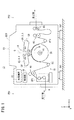
図1は、第1の実施の形態の基板(被照射体)Pに露光処理を施す露光装置EXを含むデバイス製造システム10の概略構成を示す図である。なお、以下の説明においては、XYZ直交座標系を設定し、図に示す矢印にしたがって、X方向、Y方向、およびZ方向を説明する。
[First Embodiment]
FIG. 1 is a diagram showing a schematic configuration of a device manufacturing system 10 including an exposure apparatus EX that performs an exposure process on a substrate (irradiated body) P according to the first embodiment. In the following description, an XYZ orthogonal coordinate system is set, and the X direction, the Y direction, and the Z direction will be described according to the arrows shown in the figure.

デバイス製造システム10は、例えば、デバイスとしてのフレキシブル・ディスプレイを製造するシステムである。フレキシブル・ディスプレイとしては、例えば、有機ELディスプレイ等がある。デバイス製造システム10は、フレキシブルの基板Pをロール状に巻いた図示しない供給ロールから基板Pが送出され、送出された基板Pに対して各種処理を連続的に施した後、各種処理後の基板Pを図示しない回収ロールで巻き取る、いわゆる、ロール・ツー・ロール(Roll To Roll)方式の構造を有する。そのため、各種処理後の基板Pは、複数のデバイスが連なった状態となっており、多面取り用の基板となっている。前記供給ロールから送られた基板Pは、順次、プロセス装置PR1、露光装置EX、およびプロセス装置PR2で各種処理が施され、前記回収ロールで巻き取られる。この基板Pは、基板Pの移動方向が長手方向(長尺)となり、幅方向が短手方向(短尺)となる帯状の形状を有する。   The device manufacturing system 10 is a system for manufacturing a flexible display as a device, for example. Examples of the flexible display include an organic EL display. The device manufacturing system 10 sends out a substrate P from a supply roll (not shown) obtained by winding a flexible substrate P in a roll shape, and continuously performs various processes on the delivered substrate P, and then performs various processes on the substrate P It has a so-called roll-to-roll (Roll To Roll) structure in which P is wound up by a collecting roll (not shown). For this reason, the substrate P after various treatments is in a state where a plurality of devices are connected to each other, and is a multi-sided substrate. The substrate P sent from the supply roll is sequentially subjected to various processes by the process apparatus PR1, the exposure apparatus EX, and the process apparatus PR2, and is taken up by the collection roll. The substrate P has a belt-like shape in which the moving direction of the substrate P is the longitudinal direction (long) and the width direction is the short direction (short).

なお、X方向は、水平面内において、プロセス装置PR1から露光装置EXを経てプロセス装置PR2に向かう方向(搬送方向)である。Y方向は、水平面内においてX方向に直交する方向であり、基板Pの幅方向である。Z方向は、X方向とY方向とに直交する方向(上方向)である。   The X direction is a direction (conveyance direction) from the process apparatus PR1 to the process apparatus PR2 through the exposure apparatus EX in a horizontal plane. The Y direction is a direction orthogonal to the X direction in the horizontal plane, and is the width direction of the substrate P. The Z direction is a direction (upward direction) orthogonal to the X direction and the Y direction.

基板Pは、例えば、樹脂フィルム、ステンレス鋼等の金属または合金からなる箔(フォイル)等が用いられる。樹脂フィルムの材質としては、例えば、ポリエチレン樹脂、ポリプロピレン樹脂、ポリエステル樹脂、エチレンビニル共重合体樹脂、ポリ塩化ビニル樹脂、セルロース樹脂、ポリアミド樹脂、ポリイミド樹脂、ポリカーボネート樹脂、ポリスチレン樹脂、および酢酸ビニル樹脂のうち、少なくとも1つ以上を含んだものを用いてもよい。また、基板Pの厚みや剛性(ヤング率)は、露光装置EXの搬送路を通る際に、基板Pに座屈による折れ目や非可逆的なシワが生じないような範囲であればよい。基板Pの母材として、厚みが25μm〜200μm程度のPET(ポリエチレンテレフタレート)やPEN(ポリエチレンナフタレート)等のフィルムは、好適なシート基板の典型である。   For the substrate P, for example, a foil (foil) made of a metal or an alloy such as a resin film or stainless steel is used. Examples of the resin film material include polyethylene resin, polypropylene resin, polyester resin, ethylene vinyl copolymer resin, polyvinyl chloride resin, cellulose resin, polyamide resin, polyimide resin, polycarbonate resin, polystyrene resin, and vinyl acetate resin. Among them, one containing at least one or more may be used. Further, the thickness and rigidity (Young's modulus) of the substrate P may be in a range that does not cause folds or irreversible wrinkles due to buckling in the substrate P when passing through the transport path of the exposure apparatus EX. As a base material of the substrate P, a film such as PET (polyethylene terephthalate) or PEN (polyethylene naphthalate) having a thickness of about 25 μm to 200 μm is typical of a suitable sheet substrate.

基板Pは、プロセス装置PR1、露光装置EX、およびプロセス装置PR2で施される各処理において熱を受ける場合があるため、熱膨張係数が顕著に大きくない材質の基板Pを選定することが好ましい。例えば、無機フィラーを樹脂フィルムに混合することによって熱膨張係数を抑えることができる。無機フィラーは、例えば、酸化チタン、酸化亜鉛、アルミナ、または酸化ケイ素等でもよい。また、基板Pは、フロート法等で製造された厚さ100μm程度の極薄ガラスの単層体であってもよいし、この極薄ガラスに上記の樹脂フィルム、箔等を貼り合わせた積層体であってもよい。   Since the substrate P may receive heat in each process performed by the process apparatus PR1, the exposure apparatus EX, and the process apparatus PR2, it is preferable to select the substrate P made of a material that does not have a significantly large thermal expansion coefficient. For example, the thermal expansion coefficient can be suppressed by mixing an inorganic filler with a resin film. The inorganic filler may be, for example, titanium oxide, zinc oxide, alumina, or silicon oxide. Further, the substrate P may be a single layer of ultrathin glass having a thickness of about 100 μm manufactured by a float process or the like, or a laminate in which the above resin film, foil, or the like is bonded to the ultrathin glass. It may be.

プロセス装置PR1は、露光装置EXで露光処理される基板Pに対して前工程の処理を行う。プロセス装置PR1は、前工程の処理を行った基板Pを露光装置EXへ向けて送る。この前工程の処理により、露光装置EXへ送られる基板Pは、その表面に感光性機能層(光感応層)が形成された基板(感光基板)Pとなっている。   The process apparatus PR1 performs a pre-process on the substrate P to be exposed by the exposure apparatus EX. The process apparatus PR1 sends the substrate P that has been subjected to the previous process to the exposure apparatus EX. By this pre-process, the substrate P sent to the exposure apparatus EX is a substrate (photosensitive substrate) P having a photosensitive functional layer (photosensitive layer) formed on the surface thereof.

この感光性機能層は、溶液として基板P上に塗布され、乾燥することによって層(膜)となる。感光性機能層の典型的なものはフォトレジストであるが、現像処理が不要な材料として、紫外線の照射を受けた部分の親撥液性が改質される感光性シランカップリング材(SAM)、或いは紫外線の照射を受けた部分にメッキ還元基が露呈する感光性還元材等がある。感光性機能層として感光性シランカップリング材を用いる場合は、基板P上の紫外線で露光されたパターン部分が撥液性から親液性に改質される。そのため、親液性となった部分の上に導電性インク(銀や銅等の導電性ナノ粒子を含有するインク)や半導体材料を含有した液体等を選択塗布することで、パターン層を形成することができる。感光性機能層として、感光性還元材を用いる場合は、基板P上の紫外線で露光されたパターン部分にメッキ還元基が露呈する。そのため、露光後、基板Pを直ちにパラジウムイオン等を含むメッキ液中に一定時間浸漬することで、パラジウムによるパターン層が形成(析出)される。このようなメッキ処理はアディティブ(additive)なプロセスであるが、その他、サブトラクティブ(subtractive)なプロセスとしてのエッチング処理を前提にする場合、露光装置EXへ送られる基板Pは、母材をPETやPENとし、その表面にアルミニウム(Al)や銅(Cu)等の金属性薄膜を全面または選択的に蒸着し、さらにその上にフォトレジスト層を積層したものであってもよい。   This photosensitive functional layer is applied on the substrate P as a solution and dried to form a layer (film). A typical photosensitive functional layer is a photoresist, but a photosensitive silane coupling material (SAM) whose lyophilicity is modified in a portion irradiated with ultraviolet rays as a material that does not require development processing. Alternatively, there is a photosensitive reducing material in which a plating reducing group is exposed in a portion that has been irradiated with ultraviolet rays. When a photosensitive silane coupling material is used as the photosensitive functional layer, the pattern portion exposed to ultraviolet rays on the substrate P is modified from lyophobic to lyophilic. Therefore, a pattern layer is formed by selectively applying a conductive ink (ink containing conductive nanoparticles such as silver or copper) or a liquid containing a semiconductor material on the lyophilic portion. be able to. When a photosensitive reducing material is used as the photosensitive functional layer, the plating reducing group is exposed to the pattern portion exposed to the ultraviolet rays on the substrate P. Therefore, after exposure, the substrate P is immediately immersed in a plating solution containing palladium ions or the like for a certain period of time, so that a pattern layer of palladium is formed (deposited). Such a plating process is an additive process. However, in the case of assuming an etching process as a subtractive process, the substrate P sent to the exposure apparatus EX has a base material of PET or the like. PEN may be formed by depositing a metallic thin film such as aluminum (Al) or copper (Cu) on the entire surface or selectively, and further laminating a photoresist layer thereon.

本実施の形態の場合、パターン描画装置としての露光装置EXは、マスクを用いない直描方式の露光装置、いわゆるラスタースキャン方式の露光装置EXであり、プロセス装置PR1から供給された基板Pに対して、ディスプレイ用の回路または配線等のパターンを描画する。後で詳細に説明するが、露光装置EXは、基板PをX方向に搬送しながら、露光用のレーザ光(ビーム)LBのスポット光を基板P上で所定の走査方向に走査しつつ、スポット光の強度をパターンデータ(描画データ、描画情報)に応じて高速に変調(on/off)することによって、基板Pの表面(感光面)にパターンを描画露光している。   In the case of the present embodiment, the exposure apparatus EX as a pattern drawing apparatus is a direct drawing type exposure apparatus that does not use a mask, that is, a so-called raster scan type exposure apparatus EX, and applies to the substrate P supplied from the process apparatus PR1. Then, a pattern such as a display circuit or wiring is drawn. As will be described in detail later, the exposure apparatus EX scans the spot light of the laser beam (beam) LB for exposure on the substrate P in a predetermined scanning direction while transporting the substrate P in the X direction. A pattern is drawn and exposed on the surface (photosensitive surface) of the substrate P by modulating (on / off) the intensity of light at high speed according to pattern data (drawing data, drawing information).

プロセス装置PR2は、露光装置EXで露光処理された基板Pに対しての後工程の処理(例えばメッキ処理や現像・エッチング処理等)を行う。この後工程の処理により、基板P上にデバイスのパターン層が形成される。   The process apparatus PR2 performs post-process processing (for example, plating processing, development / etching processing, etc.) on the substrate P exposed by the exposure apparatus EX. The pattern layer of the device is formed on the substrate P by the subsequent process.

露光装置EXは、光源装置(パルス光源装置、パルスレーザ装置)12と、描画ヘッド14と、基板搬送機構16と、制御部18とを備えている。光源装置12は、パルス状のレーザ光(パルス光)LBを射出するものである。このレーザ光LBは、370mm以下の波長帯域にピーク波長を有する紫外線光であり、レーザ光LBの発振周波数をFsとする。光源装置12が射出したレーザ光LBは、描画ヘッド14に入射する。描画ヘッド14は、レーザ光LBがそれぞれ入射する複数の描画ユニットU(U1〜U6)を備えている。描画ヘッド14は、基板搬送機構16によって搬送される基板Pの一部分に、複数の描画ユニットU1〜U6によって、所定のパターンを描画する。描画ヘッド14は、複数の描画ユニットU1〜U6を有することで、いわゆるマルチビーム型の描画ヘッド14となっている。基板搬送機構16は、プロセス装置PR1から搬送される基板Pを、プロセス装置PR2に所定の速度で搬送する。制御部18は、露光装置EXの各部を制御し、各部に処理を実行させる。この制御部18は、コンピュータと、プログラムが記憶された記憶媒体とを含み、該コンピュータが記憶媒体に記憶されたプログラムを実行することで、本第1の実施の形態の制御部18として機能する。   The exposure apparatus EX includes a light source device (pulse light source device, pulse laser device) 12, a drawing head 14, a substrate transport mechanism 16, and a control unit 18. The light source device 12 emits pulsed laser light (pulse light) LB. This laser beam LB is ultraviolet light having a peak wavelength in a wavelength band of 370 mm or less, and the oscillation frequency of the laser beam LB is Fs. The laser beam LB emitted from the light source device 12 enters the drawing head 14. The drawing head 14 includes a plurality of drawing units U (U1 to U6) on which the laser beams LB are incident. The drawing head 14 draws a predetermined pattern on a part of the substrate P transported by the substrate transport mechanism 16 by a plurality of drawing units U1 to U6. The drawing head 14 has a plurality of drawing units U <b> 1 to U <b> 6, thereby forming a so-called multi-beam type drawing head 14. The substrate transport mechanism 16 transports the substrate P transported from the process apparatus PR1 to the process apparatus PR2 at a predetermined speed. The control unit 18 controls each part of the exposure apparatus EX and causes each part to execute processing. The control unit 18 includes a computer and a storage medium storing a program, and the computer functions as the control unit 18 according to the first embodiment by executing the program stored in the storage medium. .

露光装置EXは、温調チャンバーECV内に格納されている。この温調チャンバーECVは、内部を所定の温度に保つことで、内部において搬送される基板Pの温度による形状変化を抑制する。温調チャンバーECVは、パッシブまたはアクティブな防振ユニットSU1、SU2を介して製造工場の設置面Eに配置される。防振ユニットSU1、SU2は、設置面Eからの振動を低減する。この設置面Eは、設置土台上の面であってもよく、床であってもよい。   The exposure apparatus EX is stored in the temperature control chamber ECV. This temperature control chamber ECV keeps the inside at a predetermined temperature, thereby suppressing the shape change due to the temperature of the substrate P transported inside. The temperature control chamber ECV is arranged on the installation surface E of the manufacturing factory via passive or active vibration isolation units SU1, SU2. The anti-vibration units SU1 and SU2 reduce vibration from the installation surface E. The installation surface E may be a surface on the installation base or a floor.

基板搬送機構16は、基板Pの搬送方向の上流側から順に、エッジポジションコントローラEPC、駆動ローラR1、テンション調整ローラRT1、回転ドラム(円筒ドラム)20、テンション調整ローラRT2、駆動ローラR2、および駆動ローラR3を有している。   The substrate transport mechanism 16 includes an edge position controller EPC, a drive roller R1, a tension adjustment roller RT1, a rotary drum (cylindrical drum) 20, a tension adjustment roller RT2, a drive roller R2, and a drive in order from the upstream side in the transport direction of the substrate P. It has a roller R3.

エッジポジションコントローラEPCは、プロセス装置PR1から搬送される基板Pの幅方向(Y方向であって基板Pの短尺方向)における位置を調整する。駆動ローラR1は、エッジポジションコントローラEPCから搬送される基板Pの表裏両面を保持しながら回転し、基板Pを回転ドラム20へ向けて搬送する。回転ドラム20は、基板P上で所定のパターンが露光される部分をその円周面で支持する。回転ドラム20は、Y方向に延びる回転軸AXを中心に回転することで、基板PをX方向に搬送する。この回転軸AXには、図示しない回転駆動源(例えば、モータや減速機構等)からの回転トルクが与えられる。この前記回転駆動源は、制御部18によって制御される。なお、便宜的に、回転軸AXを通り、Z方向に延びる面を中心面cと呼ぶ。   The edge position controller EPC adjusts the position in the width direction (the Y direction and the short direction of the substrate P) of the substrate P transported from the process apparatus PR1. The driving roller R <b> 1 rotates while holding both front and back surfaces of the substrate P conveyed from the edge position controller EPC, and conveys the substrate P toward the rotating drum 20. The rotating drum 20 supports a portion of the substrate P where a predetermined pattern is exposed on its circumferential surface. The rotary drum 20 conveys the substrate P in the X direction by rotating around a rotation axis AX extending in the Y direction. A rotational torque from a rotation drive source (not shown) (for example, a motor or a speed reduction mechanism) is applied to the rotation axis AX. The rotational drive source is controlled by the control unit 18. For convenience, a plane that passes through the rotation axis AX and extends in the Z direction is referred to as a center plane c.

駆動ローラR2、R3は、基板Pの搬送方向に沿って所定の間隔を空けて配置されており、露光後の基板Pに所定の弛み(あそび)を与えている。駆動ローラR2、R3は、駆動ローラR1と同様に、基板Pの表裏両面を保持しながら回転し、基板Pをプロセス装置PR2へ向けて搬送する。駆動ローラR2、R3は、回転ドラム20に対して搬送方向の下流側に設けられており、この駆動ローラR2は、駆動ローラR3に対して、搬送方向の上流側に設けられている。テンション調整ローラRT1、RT2は、回転ドラム20に巻き付けられて支持されている基板Pに、所定のテンションを与えている。   The drive rollers R2 and R3 are arranged at a predetermined interval along the transport direction of the substrate P, and give a predetermined slack (play) to the exposed substrate P. Similarly to the drive roller R1, the drive rollers R2 and R3 rotate while holding both front and back surfaces of the substrate P, and transport the substrate P toward the process apparatus PR2. The drive rollers R2 and R3 are provided on the downstream side in the transport direction with respect to the rotary drum 20, and the drive roller R2 is provided on the upstream side in the transport direction with respect to the drive roller R3. The tension adjusting rollers RT1 and RT2 apply a predetermined tension to the substrate P that is wound around and supported by the rotary drum 20.

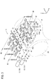
図2は、描画ヘッド14および回転ドラム20を支持する支持フレーム(装置コラム)30を示す図である。支持フレーム30は、本体フレーム32と、3点支持部34と、描画ヘッド支持部36とを有する。支持フレーム30は、温調チャンバーECV内に格納されている。本体フレーム32は、回転ドラム20と、テンション調整ローラRT1(不図示)、RT2を回転可能に支持している。3点支持部34は、本体フレーム32の上端に設けられ、回転ドラム20の上方に設けられた描画ヘッド支持部36を3点で支持する。   FIG. 2 is a view showing a support frame (device column) 30 that supports the drawing head 14 and the rotating drum 20. The support frame 30 includes a main body frame 32, a three-point support portion 34, and a drawing head support portion 36. The support frame 30 is stored in the temperature control chamber ECV. The main body frame 32 rotatably supports the rotary drum 20 and the tension adjustment rollers RT1 (not shown) and RT2. The three-point support part 34 is provided at the upper end of the main body frame 32 and supports the drawing head support part 36 provided above the rotary drum 20 at three points.

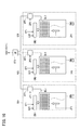
描画ヘッド支持部36は、描画ヘッド14を支持するものである。描画ヘッド支持部36は、描画ユニットU1、U3、U5を回転ドラム20の回転軸AXに対して搬送方向の下流側(+X側)で、且つ、基板Pの幅方向に沿って並列に支持する。また、描画ヘッド支持部36は、描画ユニットU2、U4、U6を回転軸AXに対して搬送方向の上流側(−X側)で、且つ、基板Pの幅方向(Y方向)に沿って並列に支持する。なお、ここで、1つの描画ユニットによるY方向の描画幅(スポット光の走査範囲)は、一例として20〜50mm程度であることから、奇数番の描画ユニットU1、U3、U5の3個と、偶数番の描画ユニットU2、U4、U6の3個との計6個の描画ユニットをY方向に配置することによって、描画可能なY方向の幅を120〜300mm程度に広げている。   The drawing head support unit 36 supports the drawing head 14. The drawing head support unit 36 supports the drawing units U1, U3, and U5 in parallel with the rotation axis AX of the rotary drum 20 on the downstream side (+ X side) in the transport direction and along the width direction of the substrate P. . In addition, the drawing head support 36 is arranged in parallel along the width direction (Y direction) of the substrate P on the upstream side (−X side) of the drawing unit U2, U4, U6 with respect to the rotation axis AX in the transport direction. To support. Here, the drawing width in the Y direction (spot light scanning range) by one drawing unit is about 20 to 50 mm as an example, and therefore, three odd numbered drawing units U1, U3, U5, By arranging a total of six drawing units including three even-numbered drawing units U2, U4, and U6 in the Y direction, the width in the Y direction that can be drawn is expanded to about 120 to 300 mm.

図3は、描画ヘッド14の構成を示す図である。本第1の実施の形態では、露光装置EXは、2つの光源装置12(12a、12b)を備える。描画ヘッド14は、複数の描画ユニットU1〜U6と、光源装置12aからのレーザ光LBを複数の描画ユニットU1、U3、U5に導く光導入光学系40aと、光源装置12bからのレーザ光LBを複数の描画ユニットU2、U4、U6に導く光導入光学系40bとを有する。   FIG. 3 is a diagram illustrating the configuration of the drawing head 14. In the first embodiment, the exposure apparatus EX includes two light source devices 12 (12a, 12b). The drawing head 14 includes a plurality of drawing units U1 to U6, a light introduction optical system 40a that guides the laser light LB from the light source device 12a to the plurality of drawing units U1, U3, and U5, and a laser light LB from the light source device 12b. And a light introducing optical system 40b led to a plurality of drawing units U2, U4, U6.

まず、図4を用いて、光導入光学系40aについて説明する。なお、光導入光学系40a、40bは、同一の構成を有するので、ここでは、光導入光学系40aについて説明し、光導入光学系40bの説明を省略する。   First, the light introducing optical system 40a will be described with reference to FIG. Since the light introducing optical systems 40a and 40b have the same configuration, the light introducing optical system 40a will be described here, and the description of the light introducing optical system 40b will be omitted.

光導入光学系40aは、光源装置12(12a)側から、集光レンズ42、コリメートレンズ44、反射ミラー46、集光レンズ48、ユニット選択用光学素子50、反射ミラー52、コリメートレンズ54、集光レンズ56、ユニット選択用光学素子58、反射ミラー60、コリメートレンズ62、集光レンズ64、ユニット選択用光学素子66、反射ミラー68、および吸収体70を有する。   The light introducing optical system 40a includes a condensing lens 42, a collimating lens 44, a reflecting mirror 46, a condensing lens 48, a unit selecting optical element 50, a reflecting mirror 52, a collimating lens 54, a collecting lens, from the light source device 12 (12a) side. It has an optical lens 56, a unit selecting optical element 58, a reflecting mirror 60, a collimating lens 62, a condenser lens 64, a unit selecting optical element 66, a reflecting mirror 68, and an absorber 70.

集光レンズ42およびコリメートレンズ44は、光源装置12aから射出されたレーザ光LBを拡大するものである。詳しくは、まず、集光レンズ42はレーザ光LBを集光レンズ42の後側の焦点位置に収斂し、コリメートレンズ44は、集光レンズ42によって収斂された後に発散するレーザ光LBを所定のビーム径(例えば、数mm)の平行光にする。   The condensing lens 42 and the collimating lens 44 expand the laser beam LB emitted from the light source device 12a. Specifically, first, the condensing lens 42 converges the laser beam LB at the focal position on the rear side of the condensing lens 42, and the collimating lens 44 applies the laser beam LB that diverges after being converged by the condensing lens 42 to a predetermined level. Parallel light with a beam diameter (for example, several mm) is used.

反射ミラー46は、コリメートレンズ44によって平行光にされたレーザ光LBを反射させてユニット選択用光学素子50に照射する。集光レンズ48は、ユニット選択用光学素子50に入射するレーザ光LBを、ユニット選択用光学素子50内でビームウェストとなるように集光(収斂)させる。ユニット選択用光学素子50は、レーザ光LBに対して透過性を有するものであり、例えば、音響光学変調素子(AOM:Acousto-Optic Modulator)が用いられる。AOMは超音波(高周波信号)を用いることで、入射したレーザ光LBを高周波の周波数に応じた回折角で回折させて、レーザ光LBの光路、つまり、進行方向を変える。AOMは、制御部18からの駆動信号のオンオフ(高周波信号のオンオフ)にしたがって、入射したレーザ光LBを回折させた回折光の発生をオンオフする。   The reflection mirror 46 reflects the laser beam LB that has been collimated by the collimator lens 44 and irradiates the unit selecting optical element 50. The condensing lens 48 condenses (converges) the laser light LB incident on the unit selecting optical element 50 so as to be a beam waist in the unit selecting optical element 50. The unit selecting optical element 50 is transmissive to the laser beam LB, and for example, an acousto-optic modulator (AOM: Acousto-Optic Modulator) is used. AOM uses ultrasonic waves (high frequency signal) to diffract the incident laser beam LB at a diffraction angle corresponding to the frequency of the high frequency, thereby changing the optical path of the laser beam LB, that is, the traveling direction. The AOM turns on / off generation of diffracted light obtained by diffracting the incident laser light LB in accordance with on / off of the drive signal from the control unit 18 (on / off of the high frequency signal).

詳しく説明すると、ユニット選択用光学素子50は、制御部18からオフの駆動信号が送られると、入射したレーザ光LBを次段のユニット選択用光学素子58に照射する。一方、制御部18からオンの駆動信号が送られると、ユニット選択用光学素子50は、入射したレーザ光LBを回折させて反射ミラー52に照射する。反射ミラー52は、入射したレーザ光LBを反射させて、描画ユニットU1のコリメートレンズ100に照射する。すなわち、制御部18がユニット選択用光学素子50をオンオフにスイッチング(駆動)することで、ユニット選択用光学素子50は、レーザ光LBを描画ユニットU1に入射させるか否かを切り換える。   More specifically, the unit selection optical element 50 irradiates the unit selection optical element 58 with the incident laser beam LB when an OFF drive signal is sent from the control unit 18. On the other hand, when an ON drive signal is sent from the control unit 18, the unit selecting optical element 50 diffracts the incident laser beam LB and irradiates the reflecting mirror 52. The reflection mirror 52 reflects the incident laser beam LB and irradiates the collimating lens 100 of the drawing unit U1. That is, when the control unit 18 switches (drives) the unit selection optical element 50 on and off, the unit selection optical element 50 switches whether or not the laser light LB is incident on the drawing unit U1.

ユニット選択用光学素子50とユニット選択用光学素子58との間には、ユニット選択用光学素子58に照射されるレーザ光LBを平行光に戻すコリメートレンズ54と、コリメートレンズ54によって平行光にされたレーザ光を再びユニット選択用光学素子58内で集光(収斂)させる集光レンズ56とが、前記の順で設けられている。   Between the unit selecting optical element 50 and the unit selecting optical element 58, a collimating lens 54 for returning the laser beam LB irradiated to the unit selecting optical element 58 to parallel light, and collimated light by the collimating lens 54. A condensing lens 56 that condenses (converges) the laser light again in the unit selecting optical element 58 is provided in the order described above.

ユニット選択用光学素子58は、ユニット選択用光学素子50と同様に、レーザ光LBに対して透過性を有するものであり、例えば、音響光学変調素子(AOM)が用いられる。ユニット選択用光学素子58は、制御部18から送られてくる駆動信号(高周波信号)がオフのときは、入射したレーザ光LBをそのまま透過してユニット選択用光学素子66に照射し、制御部18から送られてくる駆動信号(高周波信号)がオンのときは、入射したレーザ光LBを回折させて反射ミラー60に照射する。反射ミラー60は、入射したレーザ光LBを反射させて、描画ユニットU3のコリメートレンズ100に照射する。すなわち、制御部18がユニット選択用光学素子58をオンオフにスイッチングすることで、ユニット選択用光学素子58は、レーザ光LBを描画ユニットU3に入射させるか否かを切り換える。   The unit selection optical element 58 is transmissive to the laser beam LB, similarly to the unit selection optical element 50, and for example, an acousto-optic modulation element (AOM) is used. When the drive signal (high-frequency signal) sent from the control unit 18 is off, the unit selection optical element 58 transmits the incident laser beam LB as it is and irradiates the unit selection optical element 66 to the control unit. When the drive signal (high frequency signal) sent from 18 is on, the incident laser beam LB is diffracted and applied to the reflection mirror 60. The reflection mirror 60 reflects the incident laser beam LB and irradiates the collimating lens 100 of the drawing unit U3. That is, the control unit 18 switches the unit selection optical element 58 on and off, so that the unit selection optical element 58 switches whether the laser beam LB is incident on the drawing unit U3.

ユニット選択用光学素子58とユニット選択用光学素子66との間には、ユニット選択用光学素子66に照射されるレーザ光LBを平行光に戻すコリメートレンズ62と、コリメートレンズ62によって平行光にされたレーザ光を再びユニット選択用光学素子66内で集光(収斂)させる集光レンズ64とが、前記の順で設けられている。   Between the unit selecting optical element 58 and the unit selecting optical element 66, the collimating lens 62 that returns the laser beam LB irradiated to the unit selecting optical element 66 to parallel light and the collimating lens 62 makes the light parallel. The condensing lens 64 that condenses (converges) the laser light again in the unit selecting optical element 66 is provided in the order described above.

ユニット選択用光学素子66は、ユニット選択用光学素子50と同様に、レーザ光LBに対して透過性を有するものであり、例えば、音響光学変調素子(AOM)が用いられる。ユニット選択用光学素子66は、制御部18からの駆動信号(高周波信号)がオフのときは、入射したレーザ光LBを吸収体70に向けて照射し、制御部18からの駆動信号(高周波信号)がオンのときは、入射したレーザ光LBを回折させて反射ミラー68に向けて照射する。反射ミラー68は、入射したレーザ光LBを反射させて、描画ユニットU5のコリメートレンズ100に照射する。すなわち、制御部18がユニット選択用光学素子66をオンオフにスイッチングすることで、ユニット選択用光学素子66は、レーザ光LBを描画ユニットU5に入射させるか否かを切り換える。吸収体70は、レーザ光LBの外部への漏れを抑制するためのレーザ光LBを吸収する光トラップである。   The unit selecting optical element 66 is transmissive to the laser beam LB, similarly to the unit selecting optical element 50, and for example, an acousto-optic modulation element (AOM) is used. When the drive signal (high frequency signal) from the control unit 18 is off, the unit selection optical element 66 irradiates the incident laser beam LB toward the absorber 70 and the drive signal (high frequency signal) from the control unit 18. ) Is on, the incident laser beam LB is diffracted and irradiated toward the reflection mirror 68. The reflection mirror 68 reflects the incident laser beam LB and irradiates the collimating lens 100 of the drawing unit U5. That is, when the control unit 18 switches the unit selection optical element 66 on and off, the unit selection optical element 66 switches whether the laser beam LB is incident on the drawing unit U5. The absorber 70 is an optical trap that absorbs the laser beam LB for suppressing leakage of the laser beam LB to the outside.

なお、光導入光学系40bについては簡単に説明すると、光導入光学系40bのユニット選択用光学素子50、58、66は、レーザ光LBを描画ユニットU2、U4、U6に入射させるか否かを切り換える。この場合、光導入光学系40bの反射ミラー52、60、68は、ユニット選択用光学素子50、58、66から射出されるレーザ光LBを反射して描画ユニットU2、U4、U6のコリメートレンズ100に照射する。   The light introducing optical system 40b will be briefly described. The unit selecting optical elements 50, 58, and 66 of the light introducing optical system 40b determine whether or not the laser light LB is incident on the drawing units U2, U4, and U6. Switch. In this case, the reflecting mirrors 52, 60, 68 of the light introducing optical system 40b reflect the laser light LB emitted from the unit selecting optical elements 50, 58, 66 to collimate the lens 100 of the drawing units U2, U4, U6. Irradiate.

次に、図3を用いて複数の描画ユニットU1〜U6について説明する。なお、各描画ユニットU1〜U6は、同一の構成を有するので、ここでは、描画ユニットU1についてのみ説明する。   Next, a plurality of drawing units U1 to U6 will be described with reference to FIG. Since the drawing units U1 to U6 have the same configuration, only the drawing unit U1 will be described here.

描画ユニットU1は、図4に示した反射ミラー52の後のコリメートレンズ100、反射ミラー102、集光レンズ104、描画用光学素子106、コリメートレンズ108、反射ミラー110、シリンドリカルレンズ112、反射ミラー114、ポリゴンミラー(光走査部材、偏向部材)116、f−θレンズ118、シリンドリカルレンズ120、および反射ミラー122を有する。コリメートレンズ100、108、反射ミラー102、110、114、122、集光レンズ104、シリンドリカルレンズ112、120、およびf−θレンズ118は、光学レンズ系を構成する。   The drawing unit U1 includes a collimating lens 100, a reflecting mirror 102, a condenser lens 104, a drawing optical element 106, a collimating lens 108, a reflecting mirror 110, a cylindrical lens 112, and a reflecting mirror 114 after the reflecting mirror 52 shown in FIG. , A polygon mirror (light scanning member, deflection member) 116, an f-θ lens 118, a cylindrical lens 120, and a reflection mirror 122. The collimating lenses 100 and 108, the reflecting mirrors 102, 110, 114, and 122, the condensing lens 104, the cylindrical lenses 112 and 120, and the f-θ lens 118 constitute an optical lens system.

反射ミラー102は、コリメートレンズ100から入射したレーザ光LBを図3中で−Z方向に反射して、描画用光変調器としての描画用光学素子106に入射する。集光レンズ104は、描画用光学素子106に入射するレーザ光LB(平行光束)が、描画用光学素子106内でビームウェストとなるように集光(収斂)させる。描画用光学素子106は、レーザ光LBに対して透過性を有するものであり、例えば、音響光学変調素子(AOM)が用いられる。描画用光学素子106は、制御部18からの駆動信号がオフ状態のとき、入射したレーザ光LBを図示しない遮蔽板若しくは吸収体に照射し、制御部18からの駆動信号がオン状態のとき、入射したレーザ光LBを回折させて反射ミラー110に照射する。前記遮蔽板および前記吸収体は、レーザ光LBの外部への漏れを抑制するためのものである。   The reflection mirror 102 reflects the laser beam LB incident from the collimator lens 100 in the −Z direction in FIG. 3 and enters the drawing optical element 106 as a drawing light modulator. The condensing lens 104 condenses (converges) the laser beam LB (parallel light beam) incident on the drawing optical element 106 so as to be a beam waist in the drawing optical element 106. The drawing optical element 106 is transmissive to the laser beam LB, and for example, an acousto-optic modulation element (AOM) is used. The drawing optical element 106 irradiates a shielding plate or absorber (not shown) with the incident laser light LB when the drive signal from the control unit 18 is in the off state, and when the drive signal from the control unit 18 is in the on state. The incident laser beam LB is diffracted and applied to the reflection mirror 110. The shielding plate and the absorber are for suppressing leakage of the laser beam LB to the outside.

反射ミラー110と描画用光学素子106との間には、反射ミラー110に入射するレーザ光LBを平行光にするコリメートレンズ108が設けられている。反射ミラー110は、入射したレーザ光LBを反射ミラー114に照射し、反射ミラー114は、入射したレーザ光LBをポリゴンミラー116に照射する。ポリゴンミラー(回転多面鏡)116は、Z方向に延びる回転軸116aと、回転軸116aの周りに形成された複数の反射面116bとを有する。回転軸116aを中心にこのポリゴンミラー116を所定の回転方向に回転させることで、反射面116bに照射されるレーザ光LBの反射角を連続的に変化させることができる。これにより、基板P上に照射されるレーザ光LBのスポット光の位置を走査方向(基板Pの幅方向、Y方向)に走査することができる。つまり、ポリゴンミラー116は、入射したレーザ光LBを偏向させて、図5に示す走査ライン(描画ライン)L1に沿ってスポット光を走査する。なお、ポリゴンミラー116は、図示しない回転駆動源(例えば、モータや減速機構等)によって一定の速度で回転する。この回転駆動源は、制御部18によって制御される。   Between the reflection mirror 110 and the drawing optical element 106, a collimator lens 108 is provided for converting the laser light LB incident on the reflection mirror 110 into parallel light. The reflection mirror 110 irradiates the incident laser beam LB to the reflection mirror 114, and the reflection mirror 114 irradiates the incident laser beam LB to the polygon mirror 116. The polygon mirror (rotating polygonal mirror) 116 has a rotating shaft 116a extending in the Z direction and a plurality of reflecting surfaces 116b formed around the rotating shaft 116a. By rotating the polygon mirror 116 around the rotation axis 116a in a predetermined rotation direction, the reflection angle of the laser beam LB irradiated on the reflection surface 116b can be continuously changed. Thereby, the position of the spot light of the laser beam LB irradiated on the substrate P can be scanned in the scanning direction (the width direction of the substrate P, the Y direction). That is, the polygon mirror 116 deflects the incident laser light LB and scans the spot light along the scanning line (drawing line) L1 shown in FIG. The polygon mirror 116 is rotated at a constant speed by a rotation drive source (not shown) (for example, a motor or a speed reduction mechanism). This rotational drive source is controlled by the control unit 18.

反射ミラー110と反射ミラー114との間に設けられたシリンドリカルレンズ112は、走査方向と直交するZ方向(非走査方向)に関してレーザ光LBをポリゴンミラー116の反射面116b上でXY面と平行な方向に延びた長楕円状に集光する。このシリンドリカルレンズ112によって、反射面116bがZ方向(Z軸)に対して傾いている場合(面倒れ誤差がある場合)であっても、その影響を抑制することができ、基板P上に照射されるレーザ光LBによるスポット光の照射位置が、基板Pの搬送方向(X方向)にずれることを抑制する。   A cylindrical lens 112 provided between the reflection mirror 110 and the reflection mirror 114 allows the laser beam LB to be parallel to the XY plane on the reflection surface 116b of the polygon mirror 116 in the Z direction (non-scanning direction) orthogonal to the scanning direction. The light is condensed into an elliptical shape extending in the direction. Even when the reflecting surface 116b is inclined with respect to the Z direction (Z axis) (when there is a surface tilt error), the influence can be suppressed by the cylindrical lens 112, and irradiation onto the substrate P is performed. The irradiation position of the spot light by the laser beam LB is prevented from shifting in the transport direction (X direction) of the substrate P.

ポリゴンミラー116で反射したレーザ光LBは、集光レンズを含むf−θレンズ118に照射される。ポリゴンミラー116の回転角(θ/2)に応じて、f−θレンズ118への入射角がθとなる。f−θレンズ118は、その入射角θに比例した像高位置にレーザ光LBのスポット光を集光する。焦点距離をfとし、像高位置をyとすると、f−θレンズ118は、y=fθ、の関係を有する。したがって、このf−θレンズ118によって、容易に等速度の走査が可能になる。   The laser beam LB reflected by the polygon mirror 116 is applied to the f-θ lens 118 including the condenser lens. Depending on the rotation angle (θ / 2) of the polygon mirror 116, the angle of incidence on the f-θ lens 118 is θ. The f-θ lens 118 condenses the spot light of the laser light LB at an image height position proportional to the incident angle θ. When the focal length is f and the image height position is y, the f-θ lens 118 has a relationship of y = fθ. Therefore, the f-θ lens 118 can easily scan at a constant speed.

f−θレンズ118から照射されたレーザ光LBは、反射ミラー122を介して基板P上にスポット光となって照射される。f−θレンズ118と反射ミラー122との間に設けられたシリンドリカルレンズ120は、基板P上に集光されるレーザ光LBのスポット光を直径数μm程度の微小な円形にするもので、その母線はY方向と平行になっている。これにより、基板P上にはスポット光(走査スポット)によるY方向に延びた走査ラインL1(図5参照)が規定される。シリンドリカルレンズ120が無い場合、ポリゴンミラー116の手前のシリンドリカルレンズ112の作用によって、基板P上に集光するスポット光は、走査方向(Y方向)と直交した方向(X方向)に伸びた長楕円形になってしまう。   The laser beam LB emitted from the f-θ lens 118 is emitted as spot light onto the substrate P via the reflection mirror 122. The cylindrical lens 120 provided between the f-θ lens 118 and the reflection mirror 122 makes the spot light of the laser beam LB condensed on the substrate P a minute circle having a diameter of about several μm. The bus is parallel to the Y direction. Thereby, a scanning line L1 (see FIG. 5) extending in the Y direction by the spot light (scanning spot) is defined on the substrate P. When the cylindrical lens 120 is not provided, the spot light condensed on the substrate P by the action of the cylindrical lens 112 in front of the polygon mirror 116 is elongated oval extending in a direction (X direction) orthogonal to the scanning direction (Y direction). It becomes a shape.

このように、基板PがX方向に搬送されている状態で、各描画ユニットU1〜U6によって、レーザ光LBの走査スポットが走査方向(Y方向)に走査することで、所定のパターンが基板P上に描画される。この各描画ユニットU1〜U6は、基板P上の異なる領域を走査するように描画ヘッド支持部36に配置されている。なお、基板P上での走査スポットの走査方向の寸法(走査ラインの長さ)をDs、走査スポットの基板P上での走査速度をVsとしたとき、レーザ光LBの発振周波数Fsは、Fs≧Vs/Ds、の関係を満たす必要がある。レーザ光LBはパルス光であるため、発振周波数Fsが、Fs≧Vs/Ds、の関係を満たさないと、所定の間隔(隙間)を空けて基板P上にレーザ光LBの走査スポットが照射されてしまうからである。発振周波数Fsが、Fs≧Vs/Ds、の関係を満たすと、走査スポットが走査方向に関して互いに重なり合うように基板P上に照射することができるので、パルス発振するレーザ光LBであっても、走査方向に実質的に連続した直線パターンを基板P上に良好に描画することができる。   As described above, the scanning pattern of the laser beam LB is scanned in the scanning direction (Y direction) by each of the drawing units U1 to U6 in a state where the substrate P is transported in the X direction. Rendered on top. Each of the drawing units U1 to U6 is arranged on the drawing head support portion 36 so as to scan different areas on the substrate P. When the scanning spot dimension (scanning line length) on the substrate P is Ds and the scanning speed of the scanning spot on the substrate P is Vs, the oscillation frequency Fs of the laser beam LB is Fs. It is necessary to satisfy the relationship of ≧ Vs / Ds. Since the laser beam LB is pulsed light, if the oscillation frequency Fs does not satisfy the relationship of Fs ≧ Vs / Ds, a scanning spot of the laser beam LB is irradiated on the substrate P with a predetermined interval (gap). Because it will end up. When the oscillation frequency Fs satisfies the relationship of Fs ≧ Vs / Ds, the scanning spots can be irradiated onto the substrate P so as to overlap each other in the scanning direction. A linear pattern substantially continuous in the direction can be satisfactorily drawn on the substrate P.

図5は、各描画ユニットU1〜U6によって、走査スポットが走査される走査ラインL(L1〜L6)を示す図である。複数の走査ライン(描画ライン)L1〜L6は、中心面cを挟んで、回転ドラム20の周方向に2列に配置される。走査ラインL1、L3、L5は、中心面cに対して搬送方向の下流側の基板P上に位置する。走査ラインL2、L4、L6は、中心面cに対して搬送方向の上流側の基板P上に位置する。各走査ラインL1〜L6は、基板Pの幅方向、つまり、回転ドラム20の回転軸AXに沿って略平行となっており、基板Pの幅方向の長さよりも短い。   FIG. 5 is a diagram showing scanning lines L (L1 to L6) on which scanning spots are scanned by the drawing units U1 to U6. The plurality of scanning lines (drawing lines) L <b> 1 to L <b> 6 are arranged in two rows in the circumferential direction of the rotary drum 20 with the center plane c interposed therebetween. The scanning lines L1, L3, and L5 are located on the substrate P on the downstream side in the transport direction with respect to the center plane c. The scanning lines L2, L4, and L6 are located on the substrate P on the upstream side in the transport direction with respect to the center plane c. Each scanning line L1 to L6 is substantially parallel to the width direction of the substrate P, that is, along the rotation axis AX of the rotary drum 20, and is shorter than the length of the substrate P in the width direction.

走査ラインL1、L3、L5は、基板Pの幅方向に沿って所定の間隔を空けて配置され、走査ラインL2、L4、L6も同様に、基板Pの幅方向に沿って所定の間隔を空けて配置されている。このとき、走査ラインL2は、基板Pの幅方向において、走査ラインL1と走査ラインL3との間に配置される。同様に、走査ラインL3は、基板Pの幅方向において、走査ラインL2と走査ラインL4との間に配置される。走査ラインL4は、基板Pの幅方向において、走査ラインL3と走査ラインL5との間に配置される。走査ラインL5は、基板Pの幅方向において、走査ラインL4と走査ラインL6との間に配置される。すなわち、走査ラインL1〜L6は、基板P上に描画される露光領域Wの幅方向の全てをカバーするように配置される。   The scanning lines L1, L3, and L5 are arranged at predetermined intervals along the width direction of the substrate P, and the scanning lines L2, L4, and L6 are similarly spaced at predetermined intervals along the width direction of the substrate P. Are arranged. At this time, the scanning line L2 is arranged between the scanning line L1 and the scanning line L3 in the width direction of the substrate P. Similarly, the scanning line L3 is arranged between the scanning line L2 and the scanning line L4 in the width direction of the substrate P. The scanning line L4 is disposed between the scanning line L3 and the scanning line L5 in the width direction of the substrate P. The scanning line L5 is arranged between the scanning line L4 and the scanning line L6 in the width direction of the substrate P. That is, the scanning lines L1 to L6 are arranged so as to cover the entire width direction of the exposure region W drawn on the substrate P.

奇数番の走査ラインL1、L3、L5の各々に沿って走査されるレーザ光LBの走査方向は、一次元の方向となっており、同じ方向となっている。偶数番の走査ラインL2、L4、L6の各々に沿って走査されるレーザ光LBの走査方向は、一次元の方向となっており、同じ方向となっている。この走査ラインL1、L3、L5に沿って走査されるレーザ光LBの走査方向と、走査ラインL2、L4、L6に沿って走査されるレーザ光LBの走査方向とは互いに逆方向となっている。詳しくは、この走査ラインL2、L4、L6に沿って走査されるレーザ光LBの走査方向は+Y方向であり、走査ラインL1、L3、L5に沿って走査されるレーザ光LBの走査方向(−Y方向)である。これは、描画ユニットU1〜U6のポリゴンミラー116として、同一方向に回転するポリゴンミラーを使用したことによる。これにより、走査ラインL1、L3、L5の描画開始位置と、走査ラインL2、L4、L6の描画開始位置とはY方向に関して隣接する。また、走査ラインL3、L5の描画終了位置と、走査ラインL2、L4の描画終了位置とはY方向に関して隣接する。なお、走査ラインL1〜L6の各々に沿って走査されるレーザ光LB(スポット光)の走査距離は同一とする。   The scanning direction of the laser beam LB scanned along each of the odd-numbered scanning lines L1, L3, and L5 is a one-dimensional direction and is the same direction. The scanning direction of the laser beam LB scanned along each of the even-numbered scanning lines L2, L4, and L6 is a one-dimensional direction and is the same direction. The scanning direction of the laser beam LB scanned along the scanning lines L1, L3, and L5 is opposite to the scanning direction of the laser beam LB scanned along the scanning lines L2, L4, and L6. . Specifically, the scanning direction of the laser beam LB scanned along the scanning lines L2, L4, and L6 is the + Y direction, and the scanning direction of the laser beam LB scanned along the scanning lines L1, L3, and L5 (− Y direction). This is because a polygon mirror rotating in the same direction is used as the polygon mirror 116 of the drawing units U1 to U6. Thereby, the drawing start positions of the scanning lines L1, L3, and L5 and the drawing start positions of the scanning lines L2, L4, and L6 are adjacent to each other in the Y direction. The drawing end positions of the scanning lines L3 and L5 and the drawing end positions of the scanning lines L2 and L4 are adjacent to each other in the Y direction. Note that the scanning distance of the laser light LB (spot light) scanned along each of the scanning lines L1 to L6 is the same.

図6は、各描画ユニットU1〜U6のポリゴンミラー116と、走査ラインL1〜L6の走査方向との関係を示す図である。複数の描画ユニットU1、U3、U5と複数の描画ユニットU2、U4、U6とにおいては、反射ミラー114、ポリゴンミラー116、およびf−θレンズ118が中心面cに対して対称な構成となっている。このため、各描画ユニットU1〜U6のポリゴンミラー116を同一の方向(左回り)に回転させることで、各描画ユニットU1、U3、U5は、描画開始位置から描画終了位置へ向けて−Y方向にレーザ光LBの走査スポットを走査し、各描画ユニットU2、U4、U6は、描画開始位置から描画終了位置へ向けて+Y方向にレーザ光LBの走査スポットを走査することになる。なお、各描画ユニットU2、U4、U6のポリゴンミラー116の回転方向を、各描画ユニットU1、U3、U5のポリゴンミラー116の回転方向と逆方向にすることで、各描画ユニットU1〜U6のレーザ光LBの走査スポットの走査方向を同一方向(+Y方向または−Y方向)に合わせるようにしてもよい。   FIG. 6 is a diagram showing the relationship between the polygon mirror 116 of each drawing unit U1 to U6 and the scanning direction of the scanning lines L1 to L6. In the plurality of drawing units U1, U3, U5 and the plurality of drawing units U2, U4, U6, the reflection mirror 114, the polygon mirror 116, and the f-θ lens 118 are symmetric with respect to the center plane c. Yes. For this reason, by rotating the polygon mirror 116 of each drawing unit U1 to U6 in the same direction (counterclockwise), each drawing unit U1, U3, U5 is in the −Y direction from the drawing start position to the drawing end position. Then, each of the drawing units U2, U4, and U6 scans the scanning spot of the laser beam LB in the + Y direction from the drawing start position to the drawing end position. Note that the rotation direction of the polygon mirror 116 of each drawing unit U2, U4, U6 is opposite to the rotation direction of the polygon mirror 116 of each drawing unit U1, U3, U5, so that the laser of each drawing unit U1-U6. The scanning direction of the scanning spot of the light LB may be aligned with the same direction (+ Y direction or -Y direction).

ここで、ポリゴンミラー116は回転しているため、時間の経過と共に反射面116bの角度も変化する。したがって、ポリゴンミラー116の特定の反射面116bに入射したレーザ光LBを、f−θレンズ118に入射させることができるポリゴンミラー116の回転角度αは限られる。   Here, since the polygon mirror 116 is rotating, the angle of the reflecting surface 116b also changes with time. Therefore, the rotation angle α of the polygon mirror 116 that allows the laser beam LB incident on the specific reflecting surface 116 b of the polygon mirror 116 to be incident on the f-θ lens 118 is limited.

図7は、ポリゴンミラー116の反射面116bがf−θレンズ118に入射するように、レーザ光LBを反射することができるポリゴンミラー116の回転角度αを説明するための図である。回転角度βは、特定の反射面116bへのレーザ光LBの入射が開始するときのポリゴンミラー116の角度から、前記特定の反射面116bへの入射が終了するときのポリゴンミラー116の角度までの回転角度を示している。回転角度βは、ポリゴンミラー116の反射面116bの数Nによって、β≒360/Nで規定される。したがって、ポリゴンミラー116の前記特定の反射面116bに入射したレーザ光LBをf−θレンズ118に入射することができない回転角度範囲γは、γ=β−α、の関係式で表される。すなわち、この回転角度範囲γにおいては、レーザ光LBを基板P上に照射することができない。この回転角度αと回転角度範囲γとは、数式(1)の関係を有する。
γ=(360度/N)−α …(1)
(但し、Nは、ポリゴンミラー116が有する反射面116bの数)
FIG. 7 is a diagram for explaining the rotation angle α of the polygon mirror 116 that can reflect the laser beam LB so that the reflection surface 116 b of the polygon mirror 116 is incident on the f-θ lens 118. The rotation angle β is from the angle of the polygon mirror 116 when the incidence of the laser beam LB to the specific reflection surface 116b starts to the angle of the polygon mirror 116 when the incidence to the specific reflection surface 116b ends. The rotation angle is shown. The rotation angle β is defined as β≈360 / N by the number N of the reflection surfaces 116 b of the polygon mirror 116. Therefore, the rotation angle range γ in which the laser beam LB incident on the specific reflecting surface 116b of the polygon mirror 116 cannot enter the f-θ lens 118 is expressed by the relational expression γ = β−α. That is, the laser beam LB cannot be irradiated onto the substrate P in this rotation angle range γ. The rotation angle α and the rotation angle range γ have the relationship expressed by Equation (1).
γ = (360 degrees / N) −α (1)
(Where N is the number of reflecting surfaces 116b of the polygon mirror 116)

本第1の実施の形態では、ポリゴンミラー116は、8つの反射面116bを有するので、N=8、となる。したがって、数式(1)は、数式(2)で表すことができる。
γ=45度−α …(2)
In the first embodiment, since the polygon mirror 116 has eight reflecting surfaces 116b, N = 8. Therefore, Formula (1) can be expressed by Formula (2).
γ = 45 degrees−α (2)

また、有効描画期間である回転角度αと非描画期間である回転角度範囲γとは、数式(3)の関係式を有する。
γ=(m−1)×α …(3)
(但し、mは、1つの光源装置12からのレーザ光LBが入射する描画ユニットUの数)
The rotation angle α that is an effective drawing period and the rotation angle range γ that is a non-drawing period have the relational expression (3).
γ = (m−1) × α (3)
(Where m is the number of drawing units U on which the laser beam LB from one light source device 12 is incident)

本第1の実施の形態では、1つの光源装置12からのレーザ光LBを、3つの描画ユニットU(U1、U3、U5、または、U2、U4、U6)に入射させるので、mは3となる。したがって、数式(3)は、数式(4)で表すことができる。
γ=2×α …(4)
In the first embodiment, since the laser beam LB from one light source device 12 is incident on the three drawing units U (U1, U3, U5, or U2, U4, U6), m is 3. Become. Therefore, Formula (3) can be expressed by Formula (4).
γ = 2 × α (4)

数式(2)と数式(4)とから、α=15度、となる。すなわち、ポリゴンミラー116の反射面116bに入射したレーザ光LBを、f−θレンズ118に入射するように反射することができるポリゴンミラー116の回転角度αは最大で15度となる。したがって、回転角度αを15度とした場合、非描画期間である回転角度範囲γは30度(回転角度αの2倍)となり、ポリゴンミラー116が回転角度範囲γ分だけ回転する間に、ポリゴンミラー116に入射したレーザ光LBは無駄となり、非効率である。このときの描画の走査効率は1/3となる。   From Equation (2) and Equation (4), α = 15 degrees. That is, the rotation angle α of the polygon mirror 116 that can reflect the laser beam LB incident on the reflection surface 116 b of the polygon mirror 116 so as to enter the f-θ lens 118 is 15 degrees at the maximum. Therefore, when the rotation angle α is 15 degrees, the rotation angle range γ, which is a non-drawing period, is 30 degrees (twice the rotation angle α), and the polygon mirror 116 rotates while the rotation angle range γ is rotated. The laser beam LB incident on the mirror 116 is wasted and inefficient. At this time, the scanning efficiency of drawing is 1/3.

なお、有効描画期間である回転角度αは、レーザ光LBがf−θレンズ118に入射して、スポット光が走査ライン(L1〜L6)上を有効に走査可能な範囲であるが、f−θレンズ118の前側の焦点距離等によっては回転角度αも変わる。上記と同じ8面のポリゴンミラー116で有効描画期間である回転角度αが10度の場合、数式(2)より、非描画期間である回転角度範囲γは35度となり、このときの描画の走査効率は約1/4(10/45)となる。逆に、有効描画期間である回転角度αが20度の場合、数式(2)より、非描画期間である回転角度範囲γは25度となり、このときの描画の走査効率は約1/2(20/45)となる。なお、走査効率が1/2以上の場合は、レーザ光LBを振り分ける描画ユニットUの数は2つであってもよい。つまり、レーザ光LBを振り分けることができる描画ユニットUの数は、走査効率によって制限される。   Note that the rotation angle α, which is an effective drawing period, is a range in which the laser light LB is incident on the f-θ lens 118 and the spot light can be effectively scanned on the scanning lines (L1 to L6). Depending on the focal length of the front side of the θ lens 118, the rotation angle α also changes. When the rotation angle α that is the effective drawing period is 10 degrees with the same 8-sided polygon mirror 116 as described above, the rotation angle range γ that is the non-drawing period is 35 degrees according to Equation (2). The efficiency is about 1/4 (10/45). On the other hand, when the rotation angle α that is the effective drawing period is 20 degrees, the rotation angle range γ that is the non-drawing period is 25 degrees from Equation (2), and the scanning efficiency of drawing at this time is about 1/2 ( 20/45). When the scanning efficiency is 1/2 or more, the number of drawing units U that distribute the laser beam LB may be two. That is, the number of drawing units U that can distribute the laser beam LB is limited by the scanning efficiency.

そこで、本第1の実施の形態においては、1つの光源装置12からのレーザ光LBを入射させる描画ユニットUを切り換えて、レーザ光LBを3つの描画ユニットUに周期的に振り分けることで、走査効率の向上を図る。つまり、3つの描画ユニットUの描画期間(走査スポットを走査する走査期間)を、互いにずらすことで、光源装置12からのレーザ光LBを無駄にすることなく、走査効率の向上を図る。   Therefore, in the first embodiment, scanning is performed by switching the drawing unit U on which the laser light LB from one light source device 12 is incident and periodically distributing the laser light LB to the three drawing units U. Improve efficiency. That is, by shifting the drawing periods (scanning periods for scanning the scanning spots) of the three drawing units U from each other, the scanning efficiency is improved without wasting the laser light LB from the light source device 12.

図8は、光導入光学系40aと複数の描画ユニットU1、U3、U5との光路を模式化した図である。制御部18からユニット選択用光学素子(AOM)50にオンの駆動信号が送られ、ユニット選択用光学素子58、66にオフの駆動信号が送られると、ユニット選択用光学素子50は入射したレーザ光LBを回折させる。これにより、レーザ光LBは、反射ミラー52によって描画ユニットU1に入射し、描画ユニットU3、U5には入射しない。同様に、制御部18からユニット選択用光学素子(AOM)58にオンの駆動信号が送られ、ユニット選択用光学素子50、66にオフの駆動信号が送られると、オフ状態のユニット選択用光学素子50を透過したレーザ光LBがユニット選択用光学素子58に入射し、ユニット選択用光学素子58は、入射したレーザ光LBを回折させる。これにより、レーザ光LBは、反射ミラー60によって描画ユニットU3に入射し、描画ユニットU1、U5には入射しない。また、制御部18からユニット選択用光学素子(AOM)66にオンの駆動信号が送られ、ユニット選択用光学素子50、58にオフの駆動信号が送られると、オフ状態のユニット選択用光学素子50、58を透過したレーザ光LBがユニット選択用光学素子66に入射し、ユニット選択用光学素子66は、入射したレーザ光LBを回折させる。これにより、レーザ光LBは、反射ミラー68によって描画ユニットU5に入射し、描画ユニットU1、U3には入射しない。   FIG. 8 is a schematic view of the optical path between the light introducing optical system 40a and the plurality of drawing units U1, U3, U5. When an ON drive signal is sent from the control unit 18 to the unit selection optical element (AOM) 50 and an OFF drive signal is sent to the unit selection optical elements 58 and 66, the unit selection optical element 50 enters the incident laser. Diffract light LB. Thereby, the laser beam LB is incident on the drawing unit U1 by the reflecting mirror 52 and is not incident on the drawing units U3 and U5. Similarly, when an ON drive signal is sent from the control unit 18 to the unit selection optical element (AOM) 58 and an OFF drive signal is sent to the unit selection optical elements 50 and 66, the unit selection optical in the OFF state. The laser beam LB transmitted through the element 50 is incident on the unit selecting optical element 58, and the unit selecting optical element 58 diffracts the incident laser beam LB. Thereby, the laser beam LB is incident on the drawing unit U3 by the reflection mirror 60, and is not incident on the drawing units U1 and U5. Further, when an ON drive signal is sent from the control unit 18 to the unit selection optical element (AOM) 66 and an OFF drive signal is sent to the unit selection optical elements 50 and 58, the unit selection optical element in the OFF state. The laser light LB that has passed through 50 and 58 enters the unit selecting optical element 66, and the unit selecting optical element 66 diffracts the incident laser light LB. As a result, the laser beam LB is incident on the drawing unit U5 by the reflecting mirror 68 and is not incident on the drawing units U1 and U3.

このように、光導入光学系40aの複数のユニット選択用光学素子50、58、66を光源装置12aからのレーザ光LBの進行方向に沿って直列に配置したことにより、複数のユニット選択用光学素子50、58、66は、複数の描画ユニットU1、U3、U5のうちのいずれか1つの描画ユニットUにレーザ光LBを入射させるかを選択して切り換えることができる。制御部18は、レーザ光LBが入射する描画ユニットUが、例えば、描画ユニットU1→描画ユニットU3→描画ユニットU5→描画ユニットU1、というような順番で周期的に切り換わるように、複数のユニット選択用光学素子50、58、66を制御する。すなわち、複数の描画ユニットU1、U3、U5の各々に順番に所定の走査時間だけレーザ光LBが入射するように切り換える。   As described above, the plurality of unit selection optical elements 50, 58, and 66 of the light introducing optical system 40a are arranged in series along the traveling direction of the laser beam LB from the light source device 12a. The elements 50, 58, and 66 can select and switch whether the laser beam LB is incident on any one of the plurality of drawing units U1, U3, and U5. The control unit 18 includes a plurality of units such that the drawing unit U on which the laser beam LB is incident is periodically switched in the order of, for example, the drawing unit U1, the drawing unit U3, the drawing unit U5, and the drawing unit U1. The selection optical elements 50, 58 and 66 are controlled. That is, switching is performed so that the laser beam LB is incident on each of the plurality of drawing units U1, U3, and U5 in order for a predetermined scanning time.

描画ユニットU1のポリゴンミラー116は、描画ユニットU1にレーザ光LBが入射される期間に、入射したレーザ光LBをf−θレンズ118に向けて反射することができるように、その回転が制御部18によって制御されている。すなわち、描画ユニットU1にレーザ光LBが入射する期間と、描画ユニットU1によるレーザ光LBの走査スポットの走査期間(図7中の回転角度α)とは同期している。言い換えるならば、描画ユニットU1のポリゴンミラー116は、レーザ光LBが入射される期間と同期させて、描画ユニットU1に入射されたレーザ光LBの走査スポットを走査ラインL1に沿って走査するようにレーザ光LBを走査する。描画ユニットU3、U5のポリゴンミラー116も同様に、描画ユニットU3、U5にレーザ光LBが入射される期間に、入射したレーザ光LBをf−θレンズ118に反射することができるように、その回転が制御部18によって制御されている。すなわち、描画ユニットU3、U5にレーザ光LBが入射する期間と、描画ユニットU3、U5によるレーザ光LBの走査スポットの走査期間とは同期している。言い換えるならば、描画ユニットU3、U5のポリゴンミラー116は、レーザ光LBが入射される期間と同期させて、描画ユニットU3、U5に入射されたレーザ光LBの走査スポットを走査ラインL3、L5に沿って走査するようにレーザ光LBを走査する。   The rotation of the polygon mirror 116 of the drawing unit U1 is controlled by the control unit so that the incident laser beam LB can be reflected toward the f-θ lens 118 during the period when the laser beam LB is incident on the drawing unit U1. 18 is controlled. That is, the period during which the laser beam LB enters the drawing unit U1 and the scanning period of the scanning spot of the laser beam LB by the drawing unit U1 (the rotation angle α in FIG. 7) are synchronized. In other words, the polygon mirror 116 of the drawing unit U1 scans the scanning spot of the laser beam LB incident on the drawing unit U1 along the scanning line L1 in synchronization with the period in which the laser beam LB is incident. The laser beam LB is scanned. Similarly, the polygon mirror 116 of the drawing units U3 and U5 can also reflect the incident laser beam LB to the f-θ lens 118 during the period in which the laser beam LB is incident on the drawing units U3 and U5. The rotation is controlled by the control unit 18. That is, the period during which the laser beam LB is incident on the drawing units U3 and U5 is synchronized with the scanning period of the scanning spot of the laser beam LB by the drawing units U3 and U5. In other words, the polygon mirror 116 of the drawing units U3 and U5 synchronizes with the period in which the laser beam LB is incident, and causes the scanning spot of the laser beam LB incident on the drawing units U3 and U5 to the scanning lines L3 and L5. The laser beam LB is scanned so as to scan along.

このように、1つの光源装置12aからのレーザ光LBは、3つの描画ユニットU1、U3、U5のいずれか1つの描画ユニットUに時分割的に供給されるため、描画ユニットU1、U3、U5の各々のポリゴンミラー116は、回転速度を一致させつつ、その回転角度位置が一定の角度差を保つ(位相差を保つ)ように回転駆動が制御される。その制御の具体例については、後述する。   Thus, since the laser beam LB from one light source device 12a is supplied to any one of the three drawing units U1, U3, U5 in a time-sharing manner, the drawing units U1, U3, U5. Each of the polygon mirrors 116 is controlled to rotate so that the rotation angle positions thereof are kept at a constant angle difference (a phase difference is maintained) while matching the rotation speeds. A specific example of the control will be described later.

また、制御部18は、各描画ユニットU1、U3、U5から照射されるレーザ光LBの走査スポットによって基板P上に描画されるパターンを規定する描画データに基づいて、各描画ユニットU1、U3、U5の描画用光学素子106に供給される駆動信号(高周波信号)のオンオフを制御する。これにより、各描画ユニットU1、U3、U5の描画用光学素子106は、このオンオフの駆動信号に基づいて、入射したレーザ光LBを回折させて、走査スポットの強度を変調させることができる。この描画データは、例えば、描画パターンの1ドット(画素)を3×3μmとし、1ドット毎に駆動信号をオン(描画)する場合は「1」、駆動信号をオフ(非描画)とする場合は「0」の2値データをビットマップデータとして生成したものであり、各描画ユニットU毎にメモリ(RAM)内に一時的に記憶されている。   In addition, the control unit 18 controls the drawing units U1, U3, U3 based on the drawing data defining the pattern drawn on the substrate P by the scanning spot of the laser beam LB emitted from the drawing units U1, U3, U5. The on / off control of the drive signal (high frequency signal) supplied to the drawing optical element 106 of U5 is controlled. Thereby, the drawing optical element 106 of each drawing unit U1, U3, U5 can diffract the incident laser beam LB based on the on / off drive signal to modulate the intensity of the scanning spot. In this drawing data, for example, one dot (pixel) of the drawing pattern is 3 × 3 μm, and “1” is set when the drive signal is turned on (drawn) for each dot, and the drive signal is turned off (non-drawn). Is generated as binary data of “0” as bitmap data, and is temporarily stored in the memory (RAM) for each drawing unit U.

詳しく説明すると、制御部18は、レーザ光LBが入射する描画ユニットUの描画データ(「0」、「1」のビットストリーム)に基づいて、レーザ光LBが入射する描画ユニットUの描画用光学素子(AOM)106にオンオフの駆動信号を入力する。描画用光学素子106は、オンの駆動信号が入力されると入射したレーザ光LBを回折させて反射ミラー110に照射し、オフの駆動信号が入力されると、入射したレーザ光LBを図示しない前記遮蔽板若しくは前記吸収体に照射する。その結果、レーザ光LBが入射する描画ユニットUは、オンの駆動信号が描画用光学素子106に入力されると、基板P上にレーザ光LBのスポット光を照射し(走査スポットの強度が高くなる)、オフの駆動信号が描画用光学素子106に入力されると基板P上にレーザ光LBのスポット光を照射しない(走査スポットの強度が0になる)。したがって、レーザ光LBが入射する描画ユニットUは、走査ラインLに沿って、描画データに基づくパターンを基板P上に描画することができる。   More specifically, the control unit 18 draws the drawing optical of the drawing unit U into which the laser beam LB is incident based on the drawing data (bit stream of “0” and “1”) of the drawing unit U into which the laser beam LB is incident. An on / off drive signal is input to the element (AOM) 106. The drawing optical element 106 diffracts the incident laser beam LB when an ON drive signal is input and irradiates the reflection mirror 110, and when the OFF drive signal is input, the incident laser beam LB is not illustrated. Irradiate the shielding plate or the absorber. As a result, the drawing unit U into which the laser beam LB is incident irradiates the spot light of the laser beam LB onto the substrate P when the ON drive signal is input to the drawing optical element 106 (the intensity of the scanning spot is high). When the off drive signal is input to the drawing optical element 106, the spot light of the laser beam LB is not irradiated onto the substrate P (the intensity of the scanning spot becomes 0). Therefore, the drawing unit U on which the laser beam LB is incident can draw a pattern based on the drawing data on the substrate P along the scanning line L.

例えば、制御部18は、描画ユニットU3にレーザ光LBが入射する場合は、描画ユニットU3の描画データに基づいて、描画ユニットU3の描画用光学素子106をオンオフにスイッチング(駆動)する。これにより、描画ユニットU3は、走査ラインL3に沿って描画データに基づくパターンを基板P上に描画することができる。このようにして、各描画ユニットU1、U3、U5は、走査ラインL1、L3、L5に沿って走査ポットの強度を変調して、描画データに基づくパターンを基板P上に描画することができる。   For example, when the laser beam LB is incident on the drawing unit U3, the control unit 18 switches (drives) the drawing optical element 106 of the drawing unit U3 on and off based on the drawing data of the drawing unit U3. Thereby, the drawing unit U3 can draw a pattern based on the drawing data on the substrate P along the scanning line L3. In this way, each drawing unit U1, U3, U5 can draw the pattern based on the drawing data on the substrate P by modulating the intensity of the scanning pot along the scanning lines L1, L3, L5.

なお、図8を用いて、光導入光学系40aと複数の描画ユニットU1、U3、U5の動作について説明したが、光導入光学系40bと複数の描画ユニットU2、U4、U6についても同様である。簡単に説明すると、制御部18は、光源装置12bからのレーザ光LBが入射する偶数番の描画ユニットUが、例えば、描画ユニットU2→描画ユニットU4→描画ユニットU6→描画ユニットU2、というように順番に切り換わるように、複数のユニット選択用光学素子50、58、66を制御する。すなわち、複数の描画ユニットU1、U3、U5の各々に順番に所定の走査時間だけレーザ光LBが入射するように切り換える。また、制御部18は、各描画ユニットU2、U4、U6が走査ラインL2、L4、L6に沿って描画データに基づくパターンを基板P上に描画できるように、レーザ光LBが入射する描画ユニットUの描画データ(「0」、「1」のビットストリーム)に基づいて、該描画ユニットUの描画用光学素子(AOM)106を制御する。   The operation of the light introduction optical system 40a and the plurality of drawing units U1, U3, and U5 has been described with reference to FIG. 8, but the same applies to the light introduction optical system 40b and the plurality of drawing units U2, U4, and U6. . Briefly, the control unit 18 determines that the even-numbered drawing unit U on which the laser beam LB from the light source device 12b is incident is, for example, the drawing unit U2 → the drawing unit U4 → the drawing unit U6 → the drawing unit U2. The plurality of unit selecting optical elements 50, 58, and 66 are controlled so as to be switched in order. That is, switching is performed so that the laser beam LB is incident on each of the plurality of drawing units U1, U3, and U5 in order for a predetermined scanning time. Further, the control unit 18 draws the drawing unit U to which the laser beam LB is incident so that each drawing unit U2, U4, U6 can draw a pattern based on the drawing data on the substrate P along the scanning lines L2, L4, L6. The drawing optical element (AOM) 106 of the drawing unit U is controlled based on the drawing data (bit stream “0”, “1”).

以上のように、上記第1の実施の形態では、光源装置12a(12b)からのレーザ光LBの進行方向に沿って、複数のユニット選択用光学素子50、58、66を直列に配置したので、この複数のユニット選択用光学素子50、58、66によってレーザ光LBを複数の描画ユニットU1、U3、U5(描画ユニットU2、U4、U6)のうちいずれか1つの描画ユニットUに時分割で選択的に入射させることができ、レーザ光LBを無駄にすることなく、レーザ光LBの利用効率の向上を図ることができる。   As described above, in the first embodiment, the plurality of unit selecting optical elements 50, 58, and 66 are arranged in series along the traveling direction of the laser beam LB from the light source device 12a (12b). The laser light LB is time-divided into any one drawing unit U among the plurality of drawing units U1, U3, U5 (drawing units U2, U4, U6) by the plurality of unit selecting optical elements 50, 58, 66. The laser beam LB can be selectively incident and the use efficiency of the laser beam LB can be improved without wasting the laser beam LB.

また、複数(ここでは3つ)の描画ユニットUの各々のポリゴンミラー116の回転速度と回転位相とを相互に同期させると共に、複数のユニット選択用光学素子50、58、66によって各描画ユニットUにレーザ光LBが入射する期間に同期させて、走査スポットが基板P上を走査するようにレーザ光LBを走査するので、レーザ光LBを無駄にすることなく、走査効率の向上を図ることができる。   In addition, the rotation speed and the rotation phase of each of the polygon mirrors 116 of a plurality (three in this case) of drawing units U are synchronized with each other, and each drawing unit U is provided by a plurality of unit selection optical elements 50, 58, 66. Since the laser beam LB is scanned so that the scanning spot scans on the substrate P in synchronization with the period during which the laser beam LB is incident, the scanning efficiency can be improved without wasting the laser beam LB. it can.

[上記第1の実施の形態の変形例]
上記第1の実施の形態は、以下のように変形してよい。上記第1の実施の形態では、レーザ光LBを3つの描画ユニットUに振り分けるようにしたが、本変形例では、1つの光源装置12からのレーザ光LBを5つの描画ユニットUに振り分ける。
[Modification of the first embodiment]
The first embodiment may be modified as follows. In the first embodiment, the laser light LB is distributed to the three drawing units U. However, in the present modification, the laser light LB from one light source device 12 is distributed to the five drawing units U.

図9は、上記第1の実施の形態の変形例における描画ヘッド14の構成を示す図である。本変形例では、光源装置12は1つであり、描画ヘッド14は、5つの描画ユニットU(U1〜U5)を有する。なお、上記第1の実施の形態と同一の構成については同様の符号を付したり、図示を省略したりし、異なる部分のみ説明する。なお、図9において、図3中に示したシリンドリカルレンズ120は図示を省略している。   FIG. 9 is a diagram showing a configuration of the drawing head 14 in a modification of the first embodiment. In the present modification, there is one light source device 12, and the drawing head 14 has five drawing units U (U1 to U5). In addition, about the same structure as the said 1st Embodiment, the same code | symbol is attached | subjected or illustration is abbreviate | omitted and only a different part is demonstrated. In FIG. 9, the cylindrical lens 120 shown in FIG. 3 is not shown.

本変形例では、光導入光学系40a、40bに代えて、光導入光学系130が用いられる。光導入光学系130は、図10に示すように、先の図4に示した集光レンズ42、コリメートレンズ44、反射ミラー46、集光レンズ48、ユニット選択用光学素子50、反射ミラー52、コリメートレンズ54、集光レンズ56、ユニット選択用光学素子58、反射ミラー60、コリメートレンズ62、集光レンズ64、ユニット選択用光学素子66、反射ミラー68、および吸収体70に加え、さらに、ユニット選択用光学素子132、反射ミラー134、コリメートレンズ136、集光レンズ138、ユニット選択用光学素子140、反射ミラー142、コリメートレンズ144、および集光レンズ146を備える。   In this modification, a light introducing optical system 130 is used instead of the light introducing optical systems 40a and 40b. As shown in FIG. 10, the light introducing optical system 130 includes the condensing lens 42, the collimating lens 44, the reflecting mirror 46, the condensing lens 48, the unit selecting optical element 50, the reflecting mirror 52, and the like shown in FIG. In addition to the collimating lens 54, the condensing lens 56, the unit selecting optical element 58, the reflecting mirror 60, the collimating lens 62, the condensing lens 64, the unit selecting optical element 66, the reflecting mirror 68, and the absorber 70, a unit A selection optical element 132, a reflection mirror 134, a collimator lens 136, a condenser lens 138, a unit selection optical element 140, a reflection mirror 142, a collimator lens 144, and a condenser lens 146 are provided.

ユニット選択用光学素子132、コリメートレンズ136、および集光レンズ138は、集光レンズ56とユニット選択用光学素子58との間に前記の順で設けられる。したがって、本変形例では、ユニット選択用光学素子50は、制御部18からオフの駆動信号を受けると、入射したレーザ光LBをそのまま透過してユニット選択用光学素子132に照射し、集光レンズ56は、ユニット選択用光学素子132に入射するレーザ光LBを、ユニット選択用光学素子132内でビームウェストとなるように集光させる。   The unit selecting optical element 132, the collimating lens 136, and the condensing lens 138 are provided between the condensing lens 56 and the unit selecting optical element 58 in the order described above. Therefore, in the present modification, when the unit selection optical element 50 receives the OFF drive signal from the control unit 18, it transmits the incident laser light LB as it is to irradiate the unit selection optical element 132, and the condenser lens. 56 condenses the laser beam LB incident on the unit selecting optical element 132 so as to form a beam waist in the unit selecting optical element 132.

ユニット選択用光学素子132は、レーザ光LBに対して透過性を有するものであり、例えば、音響光学変調素子(AOM)が用いられる。ユニット選択用光学素子132は、制御部18からオフの駆動信号を受けると、入射したレーザ光LBをそのまま透過してユニット選択用光学素子58に照射し、制御部18からオンの駆動信号が送られると、入射したレーザ光LBを回折させて反射ミラー134に照射する。反射ミラー134は、入射したレーザ光LBを反射させて、描画ユニットU2のコリメートレンズ100に入射させる。すなわち、制御部18がユニット選択用光学素子132をオンオフにスイッチングすることで、ユニット選択用光学素子132は、レーザ光LBを描画ユニットU2に入射させるかを切り換える。コリメートレンズ136は、ユニット選択用光学素子58に照射されるレーザ光LBを平行光にするものであり、集光レンズ138は、コリメートレンズ136によって平行光にされたレーザ光LBをユニット選択用光学素子58内でビームウェストとなるように集光させる。   The unit selecting optical element 132 is transmissive to the laser beam LB, and for example, an acousto-optic modulation element (AOM) is used. When the unit selection optical element 132 receives the off drive signal from the control unit 18, the unit selection optical element 132 transmits the incident laser beam LB as it is and irradiates the unit selection optical element 58, and the control unit 18 sends an on drive signal. Then, the incident laser beam LB is diffracted and applied to the reflection mirror 134. The reflection mirror 134 reflects the incident laser beam LB so as to enter the collimating lens 100 of the drawing unit U2. That is, when the control unit 18 switches the unit selection optical element 132 on and off, the unit selection optical element 132 switches whether the laser beam LB is incident on the drawing unit U2. The collimating lens 136 converts the laser light LB applied to the unit selecting optical element 58 into parallel light, and the condenser lens 138 converts the laser light LB converted into parallel light by the collimating lens 136 into unit selecting optical. Light is condensed in the element 58 so as to be a beam waist.

ユニット選択用光学素子140、コリメートレンズ144、および集光レンズ146は、集光レンズ64とユニット選択用光学素子66との間に前記の順で設けられる。したがって、本変形例では、ユニット選択用光学素子58は、制御部18からオフの駆動信号を受けると、入射したレーザ光LBをそのまま透過してユニット選択用光学素子140に照射し、集光レンズ64は、ユニット選択用光学素子140に入射するレーザ光LBを、ユニット選択用光学素子140内でビームウェストとなるように集光させる。   The unit selecting optical element 140, the collimating lens 144, and the condenser lens 146 are provided between the condenser lens 64 and the unit selecting optical element 66 in the order described above. Therefore, in the present modification, when the unit selection optical element 58 receives the off drive signal from the control unit 18, the unit selection optical element 140 transmits the incident laser light LB as it is and irradiates the unit selection optical element 140. 64 condenses the laser beam LB incident on the unit selecting optical element 140 so as to form a beam waist in the unit selecting optical element 140.

ユニット選択用光学素子140は、レーザ光LBに対して透過性を有するものであり、例えば、音響光学変調素子(AOM)が用いられる。ユニット選択用光学素子140は、制御部18からオフの駆動信号を受けると、入射したレーザ光LBをユニット選択用光学素子66に照射し、制御部18からオンの駆動信号が送られると、入射したレーザ光LBを回折させて反射ミラー142に照射する。反射ミラー142は、入射したレーザ光LBを反射させて、描画ユニットU4のコリメートレンズ100に照射する。すなわち、制御部18がユニット選択用光学素子140をオンオフにスイッチングすることで、ユニット選択用光学素子140は、レーザ光LBを描画ユニットU4に入射させるかを切り換える。コリメートレンズ144は、ユニット選択用光学素子66に照射されるレーザ光LBを平行光にするものであり、集光レンズ146は、コリメートレンズ144によって平行光にされたレーザ光LBをユニット選択用光学素子66内でビームウェストとなるように集光させる。   The unit selecting optical element 140 is transmissive to the laser beam LB, and for example, an acousto-optic modulation element (AOM) is used. The unit selection optical element 140 irradiates the unit selection optical element 66 with the incident laser beam LB when receiving the OFF drive signal from the control unit 18, and receives the ON drive signal from the control unit 18. The reflected laser beam LB is diffracted and applied to the reflection mirror 142. The reflection mirror 142 reflects the incident laser beam LB and irradiates the collimating lens 100 of the drawing unit U4. That is, when the control unit 18 switches the unit selecting optical element 140 on and off, the unit selecting optical element 140 switches whether the laser light LB is incident on the drawing unit U4. The collimating lens 144 converts the laser light LB irradiated to the unit selecting optical element 66 into parallel light, and the condenser lens 146 converts the laser light LB converted into parallel light by the collimating lens 144 into unit selecting optical. Light is condensed in the element 66 so as to be a beam waist.

この複数のユニット選択用光学素子(AOM)50、58、66、132、140をシリアル(直列)に配置することによって、複数の描画ユニットU1〜U5のうち、いずれか1つの描画ユニットUにレーザ光LBを入射させることができる。制御部18は、レーザ光LBが入射する描画ユニットUが、例えば、描画ユニットU1→描画ユニットU2→描画ユニットU3→描画ユニットU4→描画ユニットU5→描画ユニットU1、というような順番で周期的に切り換わるように、複数のユニット選択用光学素子50、132、58、140、66を制御する。すなわち、複数の描画ユニットU1〜U5の各々に順番に所定の走査時間だけレーザ光LBが入射するように切り換える。また、各描画ユニットU1〜U5のポリゴンミラー116は、制御部18による制御の下、レーザ光LBが入射される期間と同期させて、入射されたレーザ光LBの走査スポットを走査ラインL1〜L5に沿って走査するようにレーザ光LBを走査する。   By arranging the plurality of unit selecting optical elements (AOM) 50, 58, 66, 132, and 140 in series, the laser is applied to any one of the drawing units U1 to U5. Light LB can be incident. The control unit 18 periodically changes the drawing unit U on which the laser beam LB is incident, for example, in the order of the drawing unit U1, the drawing unit U2, the drawing unit U3, the drawing unit U4, the drawing unit U5, and the drawing unit U1. The plurality of unit selecting optical elements 50, 132, 58, 140, 66 are controlled so as to be switched. That is, switching is performed so that the laser beam LB enters each of the plurality of drawing units U1 to U5 in order for a predetermined scanning time. Further, the polygon mirror 116 of each drawing unit U1 to U5 synchronizes with the period during which the laser beam LB is incident under the control of the control unit 18, and scans the scanning spot of the incident laser beam LB to the scanning lines L1 to L5. Is scanned with the laser beam LB.

すなわち、本実施の形態の場合、5つの描画ユニットU1〜U5の各ポリゴンミラー116は、回転角度位置が一定の角度分ずつ位相がずれるように同期回転する。また、本実施の形態の場合、5つの描画ユニットU1〜U5にレーザ光(ビーム)LBを時分割で振り分けるので、ポリゴンミラー116の1つの反射面116bにレーザ光LBが照射され得る角度範囲(図7中の回転角度β)と、反射面116bで反射されたレーザ光LBがf−θレンズ118に入射する最大の振れ角(図7中の角度2α)とが、β≧5αを満たすように、f−θレンズ118の前側焦点距離やポリゴンミラー116の反射面数Nが設定される。   That is, in the case of the present embodiment, the polygon mirrors 116 of the five drawing units U1 to U5 are synchronously rotated so that the rotation angle positions are shifted in phase by a certain angle. Further, in the case of the present embodiment, the laser beam (beam) LB is distributed to the five drawing units U1 to U5 in a time-sharing manner, so that the angle range (with which the laser beam LB can be irradiated onto one reflecting surface 116b of the polygon mirror 116 ( The rotation angle β) in FIG. 7 and the maximum deflection angle (angle 2α in FIG. 7) at which the laser beam LB reflected by the reflecting surface 116b is incident on the f-θ lens 118 satisfy β ≧ 5α. In addition, the front focal length of the f-θ lens 118 and the number of reflection surfaces N of the polygon mirror 116 are set.

このように、本変形例においても、レーザ光LBを無駄にすることなく、光源装置12からのレーザ光の利用効率を高めて、走査効率の向上を図ることができる。なお、本変形例では、1つの光源装置12からのレーザ光LBを5つの描画ユニットUに振り分けるようにしたが、1つの光源装置12からのレーザ光LBを2つの描画ユニットUに振り分けるようにしてもよいし、4つ、または、6つ以上の描画ユニットUに振り分けるようにしてもよい。この場合は、振り分ける描画ユニットUの数をn個とすると、ポリゴンミラー116の1つの反射面116bにレーザ光LBが照射され得る角度範囲(図7中の回転角度β)と、反射面116bで反射されたレーザ光LBがf−θレンズ118に入射する最大の振れ角(図7中の角度2α)とが、β≧n×αを満たすように、f−θレンズ118の前側焦点距離やポリゴンミラー116の反射面数Nが設定される。また、上記第1の実施の形態で説明したように、2つの光源装置12(12a、12b)からレーザ光LBを複数の描画ユニットUに振り分ける場合も、3つに限らず、任意の数の描画ユニットUに振り分けるようにしてもよい。例えば、光源装置12aからのレーザ光LBを5つの描画ユニットUに振り分け、光源装置12bからのレーザ光LBを4つの描画ユニットUに振り分けてもよい。   Thus, also in this modification, the use efficiency of the laser light from the light source device 12 can be increased and the scanning efficiency can be improved without wasting the laser light LB. In this modification, the laser light LB from one light source device 12 is distributed to the five drawing units U. However, the laser light LB from one light source device 12 is distributed to the two drawing units U. Alternatively, it may be distributed to four or six or more drawing units U. In this case, if the number of drawing units U to be distributed is n, the angle range (rotation angle β in FIG. 7) in which one reflection surface 116b of the polygon mirror 116 can be irradiated with the laser beam LB and the reflection surface 116b. The front focal length of the f-θ lens 118 and the maximum deflection angle (angle 2α in FIG. 7) at which the reflected laser light LB enters the f-θ lens 118 satisfy β ≧ n × α. The number of reflection surfaces N of the polygon mirror 116 is set. Further, as described in the first embodiment, the laser light LB from the two light source devices 12 (12a, 12b) is not limited to three, but can be any number. You may make it distribute to the drawing unit U. FIG. For example, the laser light LB from the light source device 12a may be distributed to five drawing units U, and the laser light LB from the light source device 12b may be distributed to four drawing units U.

[第2の実施の形態]
上記第1の実施の形態では、各描画ユニットU内のポリゴンミラー116の手前に描画用光学素子(AOM)106を設けるので、使用する描画用光学素子106の数が多くなり、高コストとなる。そこで、本第2の実施の形態では、1つの光源装置12からのレーザ光LBの光路上に1つの描画用光変調器(AOM)を設け、その1つの描画用光変調器を用いて複数の描画ユニットUから基板Pに照射させるレーザ光LBの強度を変調させてパターンを描画させる。すなわち、第2の実施の形態では、高い応答性が要求される描画用光変調器(AOM)を複数の描画ユニットUの手前に1つだけ配置し、各描画ユニットU側には、応答性が低くてよいユニット選択用光学素子(AOM)を配置する。
[Second Embodiment]
In the first embodiment, since the drawing optical element (AOM) 106 is provided in front of the polygon mirror 116 in each drawing unit U, the number of drawing optical elements 106 to be used is increased and the cost is increased. . Therefore, in the second embodiment, one drawing light modulator (AOM) is provided on the optical path of the laser beam LB from one light source device 12, and a plurality of drawing light modulators are used. The pattern is drawn by modulating the intensity of the laser beam LB irradiated from the drawing unit U to the substrate P. That is, in the second embodiment, only one drawing optical modulator (AOM) that requires high responsiveness is arranged in front of a plurality of drawing units U, and each drawing unit U side has responsiveness. A unit selecting optical element (AOM) that may be low is disposed.

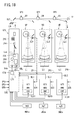
図11は、第2の実施の形態の描画ヘッド14の構成を示す図、図12は、図11に示す光導入光学系40aを示す図である。上記第1の実施の形態と同一の構成について同様の符号を付し、異なる部分のみ説明する。なお、図11において、図3中に示したシリンドリカルレンズ120は図示を省略し、光導入光学系40a、40bは、同一の構成を有するので、ここでは、光導入光学系40aについて説明し、光導入光学系40bの説明を省略する。図12に示すように、光導入光学系40aは、先の図4に示した集光レンズ42、コリメートレンズ44、反射ミラー46、集光レンズ48、ユニット選択用光学素子50、反射ミラー52、コリメートレンズ54、集光レンズ56、ユニット選択用光学素子58、反射ミラー60、コリメートレンズ62、集光レンズ64、ユニット選択用光学素子66、反射ミラー68、および吸収体70に加え、さらに、描画用光変調器としての描画用光学素子(AOM)150、コリメートレンズ152、集光レンズ154、および吸収体156を備える。本第2の実施の形態においては、図11に示すように、各描画ユニットU1〜U6内には、第1の実施の形態のような描画用光学素子106を有しない。   FIG. 11 is a diagram illustrating a configuration of the drawing head 14 according to the second embodiment, and FIG. 12 is a diagram illustrating the light introducing optical system 40a illustrated in FIG. The same reference numerals are given to the same components as those in the first embodiment, and only different parts will be described. In FIG. 11, the cylindrical lens 120 shown in FIG. 3 is not shown, and the light introduction optical systems 40a and 40b have the same configuration. Therefore, here, the light introduction optical system 40a will be described, Description of the introduction optical system 40b is omitted. As shown in FIG. 12, the light introducing optical system 40a includes the condensing lens 42, the collimating lens 44, the reflecting mirror 46, the condensing lens 48, the unit selecting optical element 50, the reflecting mirror 52, and the like shown in FIG. In addition to the collimating lens 54, the condensing lens 56, the unit selecting optical element 58, the reflecting mirror 60, the collimating lens 62, the condensing lens 64, the unit selecting optical element 66, the reflecting mirror 68, and the absorber 70, further drawing A drawing optical element (AOM) 150 serving as an optical modulator, a collimator lens 152, a condenser lens 154, and an absorber 156 are provided. In the second embodiment, as shown in FIG. 11, the drawing units U1 to U6 do not have the drawing optical element 106 as in the first embodiment.

描画用光学素子150、コリメートレンズ152、および集光レンズ154は、集光レンズ48とユニット選択用光学素子50との間に前記の順で設けられている。したがって、本第2の実施の形態においては、反射ミラー46は、コリメートレンズ44によって平行光にされたレーザ光LBを反射させて描画用光学素子150に向ける。集光レンズ48は、描画用光学素子150に入射するレーザ光LBを、描画用光学素子150内でビームウェストとなるように集光させる。   The drawing optical element 150, the collimating lens 152, and the condenser lens 154 are provided between the condenser lens 48 and the unit selecting optical element 50 in the order described above. Accordingly, in the second embodiment, the reflection mirror 46 reflects the laser beam LB that has been collimated by the collimator lens 44 and directs it toward the drawing optical element 150. The condensing lens 48 condenses the laser light LB incident on the drawing optical element 150 so as to form a beam waist in the drawing optical element 150.

描画用光学素子150は、レーザ光LBに対して透過性を有するものであり、例えば、音響光学変調素子(AOM)が用いられる。描画用光学素子150は、ユニット選択用光学素子50、58、66のうち、最も光源装置12(12a)側に位置する初段のユニット選択用光学素子50よりも光源装置12(12a)側に設けられている。描画用光学素子150は、制御部18からオフの駆動信号が送られると、入射したレーザ光LBを吸収体156に照射し、制御部18からオンの駆動信号が送られると、入射したレーザ光LBを回折させて初段のユニット選択用光学素子50に照射する。コリメートレンズ152は、ユニット選択用光学素子50に照射されるレーザ光LBを平行光にするものであり、集光レンズ154は、コリメートレンズ152によって平行光にされたレーザ光LBをユニット選択用光学素子50内でビームウェストとなるように集光させる。   The drawing optical element 150 is transmissive to the laser beam LB, and for example, an acousto-optic modulation element (AOM) is used. The drawing optical element 150 is provided closer to the light source device 12 (12a) than the first stage unit selecting optical element 50 located closest to the light source device 12 (12a) among the unit selecting optical elements 50, 58, and 66. It has been. The drawing optical element 150 irradiates the absorber 156 with the incident laser light LB when an off drive signal is sent from the control unit 18, and enters the laser beam when the on drive signal is sent from the control unit 18. The LB is diffracted and irradiated to the first-stage unit selection optical element 50. The collimating lens 152 converts the laser light LB applied to the unit selecting optical element 50 into parallel light, and the condensing lens 154 converts the laser light LB converted into parallel light by the collimating lens 152 into unit selecting optical. The light is condensed in the element 50 so as to be a beam waist.

図11に示すように、描画ユニットU1〜U6は、コリメートレンズ100、反射ミラー102、反射ミラー110、シリンドリカルレンズ112、反射ミラー114、ポリゴンミラー116、f−θレンズ118、シリンドリカルレンズ120(図11では図示を省略)、および反射ミラー122を有し、さらに、ビーム成形レンズとしての第1成形レンズ158aおよび第2成形レンズ158bとを有する。つまり、本第2の実施の形態においては、第1の実施の形態の集光レンズ104およびコリメートレンズ108に代えて、第1成形レンズ158aおよび第2成形レンズ158bが描画ユニットU1〜U6に設けられている。   As shown in FIG. 11, the drawing units U1 to U6 include a collimating lens 100, a reflecting mirror 102, a reflecting mirror 110, a cylindrical lens 112, a reflecting mirror 114, a polygon mirror 116, an f-θ lens 118, and a cylindrical lens 120 (FIG. 11). , And a reflecting mirror 122, and further, a first molded lens 158a and a second molded lens 158b as beam-shaped lenses. That is, in the second embodiment, instead of the condensing lens 104 and the collimating lens 108 of the first embodiment, a first molded lens 158a and a second molded lens 158b are provided in the drawing units U1 to U6. It has been.

図13は、図12の光導入光学系40aと複数の描画ユニットU1、U3、U5との光路を模式化した図である。制御部18は、各描画ユニットU1、U3、U5から照射されるレーザ光LBの走査スポットによって基板P上に描画されるパターンを規定する描画データ(ビットストリーム)に基づいて、光導入光学系40aの描画用光学素子150にオンオフの駆動信号を出力する。これにより、光導入光学系40aの描画用光学素子150は、このオンオフの駆動信号に基づいて、入射したレーザ光LBを回折させて、走査スポットの強度を変調(On/Off)させることができる。   FIG. 13 is a diagram schematically showing an optical path between the light introducing optical system 40a of FIG. 12 and a plurality of drawing units U1, U3, U5. Based on the drawing data (bit stream) defining the pattern drawn on the substrate P by the scanning spot of the laser beam LB emitted from each of the drawing units U1, U3, U5, the control unit 18 is based on the light introducing optical system 40a. An on / off drive signal is output to the drawing optical element 150. Accordingly, the drawing optical element 150 of the light introducing optical system 40a can diffract the incident laser light LB based on the on / off drive signal to modulate (On / Off) the intensity of the scanning spot. .

詳しく説明すると、制御部18は、レーザ光LBが入射する描画ユニットUの描画データに基づいて、描画用光学素子150にオンオフの駆動信号を入力する。描画用光学素子150は、オンの駆動信号が入力されると入射したレーザ光LBを回折させて、ユニット選択用光学素子50に照射する(ユニット選択用光学素子50に入射するレーザ光LBの強度が高くなる)。一方、描画用光学素子150は、オフの駆動信号が入力されると、入射したレーザ光LBを吸収体156(図12)に照射する(ユニット選択用光学素子50に入射するレーザ光LBの強度が0になる)。したがって、レーザ光LBが入射する描画ユニットUは、走査ラインLに沿って、強度が変調したレーザ光LBを基板Pに照射することができ、描画データに基づくパターンを基板P上に描画することができる。   More specifically, the control unit 18 inputs an on / off drive signal to the drawing optical element 150 based on the drawing data of the drawing unit U on which the laser beam LB is incident. When an ON drive signal is input, the drawing optical element 150 diffracts the incident laser light LB and irradiates the unit selecting optical element 50 (the intensity of the laser light LB incident on the unit selecting optical element 50). Becomes higher). On the other hand, the drawing optical element 150 irradiates the absorber 156 (FIG. 12) with the incident laser light LB when the OFF drive signal is input (the intensity of the laser light LB incident on the unit selecting optical element 50). Becomes 0). Therefore, the drawing unit U on which the laser beam LB is incident can irradiate the substrate P with the laser beam LB whose intensity is modulated along the scanning line L, and draws a pattern based on the drawing data on the substrate P. Can do.

例えば、描画ユニットU3にレーザ光LBが入射する場合は、制御部18は、描画ユニットU3の描画データに基づいて、光導入光学系40aの描画用光学素子150をオンオフにスイッチングする。これにより、描画ユニットU3は、走査ラインL3に沿って、強度が変調したレーザ光LBを基板Pに照射することができ、描画データに基づくパターンを基板P上に描画することができる。レーザ光LBが入射する描画ユニットUは、例えば、描画ユニットU1→描画ユニットU3→描画ユニットU5→描画ユニットU1、というように、順次切り換わる。したがって、制御部18は、同様に、描画ユニットU1の描画データ→描画ユニットU3の描画データ→描画ユニットU5の描画データ→描画ユニットU1の描画データというように、光導入光学系40aの描画用光学素子150に送るオンオフ信号を決定する描画データを順次切り換える。そして、制御部18は、順次切り換えた描画データに基づいて光導入光学系40aの描画用光学素子150を制御する。これにより、各描画ユニットU1、U3、U5は、走査ラインL1、L3、L5に沿って、強度が変調したレーザ光LBを基板Pに照射することで、描画データに応じたパターンを基板P上に描画することができる。   For example, when the laser beam LB is incident on the drawing unit U3, the control unit 18 switches the drawing optical element 150 of the light introduction optical system 40a on and off based on the drawing data of the drawing unit U3. Thereby, the drawing unit U3 can irradiate the substrate P with the laser beam LB whose intensity is modulated along the scanning line L3, and can draw a pattern based on the drawing data on the substrate P. The drawing unit U to which the laser beam LB enters is sequentially switched in the order of, for example, the drawing unit U1 → the drawing unit U3 → the drawing unit U5 → the drawing unit U1. Therefore, similarly, the control unit 18 draws the drawing light of the light introducing optical system 40a, such as drawing data of the drawing unit U1, drawing data of the drawing unit U3, drawing data of the drawing unit U5, drawing data of the drawing unit U1. The drawing data for determining the on / off signal to be sent to the element 150 is sequentially switched. Then, the control unit 18 controls the drawing optical element 150 of the light introducing optical system 40a based on the sequentially switched drawing data. Thereby, each drawing unit U1, U3, U5 irradiates the substrate P with the laser beam LB whose intensity is modulated along the scanning lines L1, L3, L5, so that a pattern corresponding to the drawing data is formed on the substrate P. Can be drawn.

以上、第2の実施の形態に適用される制御系の一部の構成とその動作について、図14〜図16を参照して詳述する。なお、以下説明する構成および動作は、第1の実施の形態にも適用可能である。図14は、一例として、図11、図13中の3つの描画ユニットU1、U3、U5の各々に設けられるポリゴンミラー116の回転制御系のブロック図であり、描画ユニットU1、U3、U5の構成は同じなので、同じ部材には同じ符号を付してある。描画ユニットU1、U3、U5の各々には、ポリゴンミラー116によって基板P上に生成される走査ライン(描画ライン)L1、L3、L5の走査開始タイミングを光電的に検知する原点センサーSz1、Sz3、Sz5が設けられる。原点センサーSz1、Sz3、Sz5は、ポリゴンミラー116の反射面116bに光を投射して、その反射光を受光する光電検出器であり、スポット光が走査ラインL1、L3、L5の走査開始点の直前の位置に来る度に、パルス状の原点信号ZP1、ZP3、ZP5を各々出力する。   The partial configuration and operation of the control system applied to the second embodiment will be described in detail with reference to FIGS. Note that the configurations and operations described below are also applicable to the first embodiment. FIG. 14 is a block diagram of the rotation control system of the polygon mirror 116 provided in each of the three drawing units U1, U3, U5 in FIGS. 11 and 13 as an example, and the configuration of the drawing units U1, U3, U5. Are the same, the same members are given the same reference numerals. Each of the drawing units U1, U3, U5 includes origin sensors Sz1, Sz3, which photoelectrically detect scanning start timings of the scanning lines (drawing lines) L1, L3, L5 generated on the substrate P by the polygon mirror 116. Sz5 is provided. The origin sensors Sz1, Sz3, and Sz5 are photoelectric detectors that project light onto the reflecting surface 116b of the polygon mirror 116 and receive the reflected light, and the spot light is a scanning start point of the scanning lines L1, L3, and L5. Each time it comes to the immediately preceding position, it outputs pulse-like origin signals ZP1, ZP3, ZP5, respectively.

タイミング計測部180は、原点信号ZP1、ZP3、ZP5を入力し、原点信号ZP1、ZP3、ZP5の各々の発生タイミングが所定の許容範囲(時間間隔)内になっているか否かを計測し、その許容範囲からの誤差が生じたら、それに応じた偏差情報をサーボ制御部182に出力する。サーボ制御部182は、各描画ユニットU1、U3、U5内のポリゴンミラー116を回転駆動するモータMpの各サーボ駆動回路部に、偏差情報に基づいた指令値を出力する。モータMpの各サーボ駆動回路部は、モータMpの回転軸に取り付けられたエンコーダENからのアップ・ダウンパルス信号(以下、エンコーダ信号)を入力して、ポリゴンミラー116の回転速度に応じた速度信号を出力する帰還回路部FBCと、サーボ制御部182からの指令値と帰還回路部FBCからの速度信号とを入力して、指令値に応じた回転速度になるようにモータMpを駆動するサーボ駆動回路(アンプ)SCCとで構成される。なお、サーボ駆動回路部(帰還回路部FBC、サーボ駆動回路SCC)、タイミング計測部180、および、サーボ制御部182は、制御部18の一部を構成する。   The timing measurement unit 180 receives the origin signals ZP1, ZP3, ZP5, measures whether the generation timing of each of the origin signals ZP1, ZP3, ZP5 is within a predetermined allowable range (time interval), If an error from the allowable range occurs, deviation information corresponding to the error is output to the servo controller 182. The servo control unit 182 outputs a command value based on the deviation information to each servo drive circuit unit of the motor Mp that rotationally drives the polygon mirror 116 in each drawing unit U1, U3, U5. Each servo drive circuit section of the motor Mp inputs an up / down pulse signal (hereinafter referred to as an encoder signal) from an encoder EN attached to the rotation shaft of the motor Mp, and a speed signal corresponding to the rotational speed of the polygon mirror 116. Servo circuit that inputs the command value from the servo control unit 182 and the speed signal from the feedback circuit unit FBC, and drives the motor Mp so that the rotation speed is in accordance with the command value. It is composed of a circuit (amplifier) SCC. The servo drive circuit unit (feedback circuit unit FBC, servo drive circuit SCC), timing measurement unit 180, and servo control unit 182 constitute part of the control unit 18.

本第2の実施の形態では、3つの描画ユニットU1、U3、U5内の各ポリゴンミラー116が、その回転角度位置に一定の位相差を保ちつつ同じ速度で回転させる必要があり、それを実現するために、タイミング計測部180は原点信号ZP1、ZP3、ZP5を入力し、例えば、図15のタイミングチャートに示すような計測を行う。   In the second embodiment, each polygon mirror 116 in the three drawing units U1, U3, and U5 needs to be rotated at the same speed while maintaining a constant phase difference at the rotation angle position, which is realized. Therefore, the timing measurement unit 180 inputs the origin signals ZP1, ZP3, and ZP5, and performs measurement as shown in the timing chart of FIG. 15, for example.

図15は、3つのポリゴンミラー116が、回転角度に関して所定の許容範囲内の位相差で回転している場合に生成される各種の信号波形を模式的に示す。各ポリゴンミラー116を回転させた直後は、原点信号ZP1、ZP3、ZP5の相対的な位相差はばらばらであるが、タイミング計測部180は、例えば、原点信号ZP1を基準として、他の原点信号ZP3、ZP5が原点信号ZP1と同じ周波数(周期)で発生し、且つ3つの原点信号ZP1、ZP3、ZP5間の時間間隔Ts1、Ts2、Ts3が共に等しい状態を基準値とし、それに対する誤差に応じた補正情報を計測する。タイミング計測部180は、その補正情報をサーボ制御部182に出力し、それによって描画ユニットU3、U5の各モータMpがサーボ制御され、3つの原点信号ZP1、ZP3、ZP5の発生タイミングが、図15のようにTs1=Ts2=Ts3で安定するように制御される。   FIG. 15 schematically shows various signal waveforms generated when the three polygon mirrors 116 are rotated with a phase difference within a predetermined allowable range with respect to the rotation angle. Immediately after each polygon mirror 116 is rotated, the relative phase differences of the origin signals ZP1, ZP3, and ZP5 vary, but the timing measurement unit 180, for example, uses another origin signal ZP3 based on the origin signal ZP1. , ZP5 is generated at the same frequency (period) as the origin signal ZP1, and the time intervals Ts1, Ts2, and Ts3 between the three origin signals ZP1, ZP3, and ZP5 are all equal to each other as a reference value, and an error corresponding thereto is determined. Measure correction information. The timing measurement unit 180 outputs the correction information to the servo control unit 182, thereby servo-controlling the motors Mp of the drawing units U3 and U5, and the generation timings of the three origin signals ZP1, ZP3, and ZP5 are shown in FIG. In this way, control is performed so as to stabilize at Ts1 = Ts2 = Ts3.

原点信号ZP1、ZP3、ZP5の発生タイミングが安定すると、タイミング計測部180は、先の図11〜図13中に示したユニット選択用光学素子50、58、66の各々に、描画イネーブル(On)信号SP1、SP3、SP5を出力する。描画イネーブル(On)信号SP1、SP3、SP5は、ここではHレベルの期間中だけ、対応するユニット選択用光学素子50、58、66に変調動作(光の偏向スイッチング動作)を行わせる。3つの原点信号ZP1、ZP3、ZP5が安定して一定の位相差(ここでは原点信号ZP1の周期の1/3)に維持されることから、描画イネーブル信号SP1、SP3、SP5の各立上り(L→H)も一定の位相差を持つ。   When the generation timings of the origin signals ZP1, ZP3, and ZP5 are stabilized, the timing measurement unit 180 applies drawing enable (On) to each of the unit selection optical elements 50, 58, and 66 shown in FIGS. Signals SP1, SP3 and SP5 are output. The drawing enable (On) signals SP1, SP3, SP5 here cause the corresponding unit selection optical elements 50, 58, 66 to perform a modulation operation (light deflection switching operation) only during the H level period. Since the three origin signals ZP1, ZP3, and ZP5 are stably maintained at a constant phase difference (here, 1/3 of the period of the origin signal ZP1), each rising edge (L → H) also has a certain phase difference.

描画イネーブル信号SP1、SP3、SP5の降下(H→L)のタイミングは、各走査ラインL1、L3、L5内でスポット光をOn/Offするためのクロック信号CLKを、タイミング計測部180内のカウンタで計測することで設定される。そのクロック信号CLKは、描画用光学素子150(或いは図3中の描画用光学素子106)のOn/Offのタイミングをつかさどるものであり、走査ライン(L1、L3、L5)の長さ、スポット光の基板P上での寸法、スポット光の走査速度等によって決まる。例えば、走査ラインLの長さが30mm、スポット光の寸法(直径)が6μmであり、スポット光を走査方向に3μmずつオーバーラップさせてOn/Offさせる場合、タイミング計測部180内のカウンタは、クロック信号CLKを10000カウント(30mm/3μm)したら、描画イネーブル信号SP1、SP3、SP5を降下(H→L)させればよい。   The timing of the drop (H → L) of the drawing enable signals SP 1, SP 3, SP 5 is the clock signal CLK for turning on / off the spot light in each scanning line L 1, L 3, L 5 and the counter in the timing measuring unit 180. It is set by measuring with. The clock signal CLK controls the On / Off timing of the drawing optical element 150 (or the drawing optical element 106 in FIG. 3), the length of the scanning lines (L1, L3, L5), and the spot light. Depending on the size on the substrate P, the scanning speed of the spot light, and the like. For example, when the length of the scanning line L is 30 mm and the dimension (diameter) of the spot light is 6 μm, and the spot light is overlapped by 3 μm in the scanning direction and turned on / off, the counter in the timing measuring unit 180 is When the clock signal CLK is counted 10,000 (30 mm / 3 μm), the drawing enable signals SP1, SP3, SP5 may be lowered (H → L).

また、ポリゴンミラー116の反射面116bを10面とし、その回転速度をVr(rpm)とすると、各原点信号ZP1、ZP3、ZP5の周波数は、10Vr/60(Hz)となる。したがって、時間間隔がTs1=Ts2=Ts3に安定した場合、時間間隔Ts1は、60/(30Vr)秒となる。一例として、ポリゴンミラー116の基準の回転速度Vrを8000rpmとすると、時間間隔Ts1は、60/(30・8000)秒=250μSとなる。   Further, assuming that the reflecting surface 116b of the polygon mirror 116 is 10 surfaces and the rotation speed is Vr (rpm), the frequencies of the origin signals ZP1, ZP3, ZP5 are 10 Vr / 60 (Hz). Therefore, when the time interval is stabilized at Ts1 = Ts2 = Ts3, the time interval Ts1 is 60 / (30 Vr) seconds. As an example, if the reference rotation speed Vr of the polygon mirror 116 is 8000 rpm, the time interval Ts1 is 60 / (30 · 8000) seconds = 250 μS.

図15のように、描画イネーブル信号SP1、SP3、SP5のOn時間(Hレベルの継続時間)Toaは、ポリゴンミラー116からのレーザ光(ビーム)LBが基板P上にスポット光として投射される期間(投射期間)であるが、時間間隔Ts1よりも短く設定する必要がある。そこで、例えば、On時間Toaを200μSに設定すると、この間に10000カウントするためのクロック信号CLKの周波数は、10000/200=50(MHz)となる。このようなクロック信号CLKに同期して、描画データ(ビットマップ上の「0」または「1」)から生成される走査ラインLに対応した描画ビット列データ(10000ビット分)Sdwが、描画用光学素子150に出力される。なお、図3のように、描画ユニットU1、U3、U5の各々に、描画用光学素子106が設けられる構成では、走査ラインL1に対応した描画ビット列データSdwは描画ユニットU1の描画用光学素子106に送られ、走査ラインL3に対応した描画ビット列データSdwは描画ユニットU3の描画用光学素子106に送られ、走査ラインL5に対応した描画ビット列データSdwは描画ユニットU5の描画用光学素子106に送られる。   As shown in FIG. 15, the On time (H level duration) Toa of the drawing enable signals SP1, SP3, SP5 is a period during which the laser beam (beam) LB from the polygon mirror 116 is projected as a spot beam on the substrate P. Although it is a (projection period), it is necessary to set shorter than time interval Ts1. Therefore, for example, if the On time Toa is set to 200 μS, the frequency of the clock signal CLK for counting 10,000 during this period is 10000/200 = 50 (MHz). In synchronization with the clock signal CLK, the drawing bit string data (for 10,000 bits) Sdw corresponding to the scanning line L generated from the drawing data (“0” or “1” on the bitmap) is used as the drawing optical. Output to the element 150. As shown in FIG. 3, in the configuration in which the drawing optical elements 106 are provided in the drawing units U1, U3, and U5, the drawing bit string data Sdw corresponding to the scanning line L1 is the drawing optical element 106 of the drawing unit U1. The drawing bit string data Sdw corresponding to the scanning line L3 is sent to the drawing optical element 106 of the drawing unit U3, and the drawing bit string data Sdw corresponding to the scanning line L5 is sent to the drawing optical element 106 of the drawing unit U5. It is done.

本第2の実施の形態では、3つの走査ラインL1、L3、L5の各々に対応した描画データから生成される描画ビット列データSdwが、描画イネーブル信号SP1、SP3、SP5(または原点信号ZP1、ZP3、ZP5)に同期して順番に描画用光学素子150のOn/Offのために供給される。   In the second embodiment, the drawing bit string data Sdw generated from the drawing data corresponding to each of the three scanning lines L1, L3, and L5 are drawn enable signals SP1, SP3, SP5 (or origin signals ZP1, ZP3). , ZP5) are sequentially supplied for On / Off of the drawing optical element 150.

図16は、そのような描画ビット列データSdwを生成する回路の一例を示し、該回路は、生成回路(描画データ生成回路)501、503、505と、OR回路GT4とを有する。生成回路501は、メモリ部BM1、カウンタ部CN1、および、ゲート部GT1を備え、生成回路503は、メモリ部BM3、カウンタ部CN3、および、ゲート部GT3を備え、生成回路505は、メモリ部BM5、カウンタ部CN5、および、ゲート部GT5を備える。この生成回路501、503、505、および、OR回路GT4は、制御部18の一部を構成する。   FIG. 16 shows an example of a circuit that generates such drawing bit string data Sdw. The circuit includes generation circuits (drawing data generation circuits) 501, 503, and 505, and an OR circuit GT4. The generation circuit 501 includes a memory unit BM1, a counter unit CN1, and a gate unit GT1, the generation circuit 503 includes a memory unit BM3, a counter unit CN3, and a gate unit GT3, and the generation circuit 505 includes a memory unit BM5. Counter part CN5 and gate part GT5. The generation circuits 501, 503, and 505 and the OR circuit GT4 constitute a part of the control unit 18.

メモリ部BM1、BM3、BM5は各描画ユニットU1、U3、U5が描画露光すべきパターンに対応したビットマップデータを一次記憶するメモリである。カウンタ部CN1、CN3、CN5は、各メモリ部BM1、BM3、BM5内のマップデータのうち、次に描画すべき1走査ライン分のビット列(例えば、10000ビット)を1ビットずつクロック信号CLKに同期したシリアルデータDL1、DL3、DL5として、描画イネーブル信号SP1、SP3、SP5がOnの期間中に出力させるためのカウンタである。   The memory units BM1, BM3, and BM5 are memories that temporarily store bitmap data corresponding to patterns to be drawn and exposed by the drawing units U1, U3, and U5. The counter units CN1, CN3, and CN5 synchronize a bit string (for example, 10,000 bits) for one scanning line to be drawn next among the map data in each of the memory units BM1, BM3, and BM5 with the clock signal CLK bit by bit. This is a counter for outputting the drawing enable signals SP1, SP3, SP5 as the serial data DL1, DL3, DL5 during the period of On.

各メモリ部BM1、BM3、BM5内のマップデータは、不図示のアドレスカウンタ等によって、1走査ライン分のデータごとシフトされる。そのシフトは、例えば、メモリ部BM1であれば、1走査ライン分のシリアルデータDL1を出力し終わった後で、次にアクティブとなる描画ユニットU3の原点信号ZP3が発生したタイミングで行われる。同様に、メモリ部BM3内のマップデータのシフトは、シリアルデータDL3が出力し終わった後で、次にアクティブとなる描画ユニットU5の原点信号ZP5が発生したタイミングで行われ、メモリ部BM5内のマップデータのシフトは、シリアルデータDL5が出力し終わった後で、次にアクティブとなる描画ユニットU1の原点信号ZP1が発生したタイミングで行われる。   The map data in each of the memory units BM1, BM3, and BM5 is shifted by data for one scanning line by an address counter (not shown) or the like. For example, in the case of the memory unit BM1, the shift is performed at the timing when the origin signal ZP3 of the drawing unit U3 that becomes the next active after the serial data DL1 for one scanning line has been output. Similarly, the shift of the map data in the memory unit BM3 is performed at the timing when the origin signal ZP5 of the drawing unit U5 that becomes the next active is generated after the serial data DL3 has been output. The shift of the map data is performed at the timing when the origin signal ZP1 of the drawing unit U1 that becomes the next active after the serial data DL5 has been output.

このようにして順次生成される各シリアルデータDL1、DL3、DL5は、描画イネーブル信号SP1、SP3、SP5のOn期間中に開かれるゲート部GT1、GT3、GT5を通って、3入力のOR回路GT4に印加される。OR回路GT4は、シリアルデータDL1→DL3→DL5→DL1・・・の順に繰り返し合成したビットデータ列を描画ビット列データSdwとして描画用光学素子150のOn/Offのために出力する。なお、図3のように、描画ユニットU1、U3、U5の各々に、描画用光学素子106が設けられる構成では、ゲート部GT1から出力されるシリアルデータDL1を描画ユニットU1内の描画用光学素子106に送り、ゲート部GT3から出力されるシリアルデータDL3を描画ユニットU3内の描画用光学素子106に送り、ゲート部GT5から出力されるシリアルデータDL5を描画ユニットU5内の描画用光学素子106に送ればよい。   Each serial data DL1, DL3, DL5 sequentially generated in this way passes through the gate portions GT1, GT3, GT5 opened during the On period of the drawing enable signals SP1, SP3, SP5, and the 3-input OR circuit GT4. To be applied. The OR circuit GT4 outputs a bit data string repeatedly synthesized in the order of serial data DL1-> DL3-> DL5-> DL1... As On / Off of the drawing optical element 150 as drawing bit string data Sdw. As shown in FIG. 3, in the configuration in which the drawing optical element 106 is provided in each of the drawing units U1, U3, U5, the serial data DL1 output from the gate part GT1 is used as the drawing optical element in the drawing unit U1. The serial data DL3 output from the gate part GT3 is sent to the drawing optical element 106 in the drawing unit U3, and the serial data DL5 output from the gate part GT5 is sent to the drawing optical element 106 in the drawing unit U5. Send it.

以上のように、描画用光学素子150(或いは106)のOn/Offは、高速なクロック信号CLK(例えば50MHz)に応答する必要があるが、ユニット選択用光学素子50、58、66は、描画イネーブル信号SP1、SP3、SP5(または原点信号ZP1、ZP3、ZP5)に同期して、On/Offを行えばよく、その応答周波数は、先の数値例の場合、時間間隔Toa(またはTs1)が200μSであったので10KHz程度でよく、透過率が高く安価なものを利用できる。なお、タイミング計測部180内のカウンタで計数されたり、図16中のカウンタ部CN1、CN3、CN5で計数されるクロック信号CLKの周波数をFcc、光源装置12からのレーザ光LBのパルス発振の基本周波数をFsとすると、nを1以上(好ましくはn≧2)の整数として、n・Fcc=Fsの関係を満たすように設定するのがよい。   As described above, On / Off of the drawing optical element 150 (or 106) needs to respond to a high-speed clock signal CLK (for example, 50 MHz), but the unit selecting optical elements 50, 58, and 66 are drawn. The On / Off may be performed in synchronization with the enable signals SP1, SP3, SP5 (or the origin signals ZP1, ZP3, ZP5), and the response frequency is the time interval Toa (or Ts1) in the case of the above numerical example. Since it was 200 μS, it may be about 10 KHz, and a high transmittance and inexpensive one can be used. Note that the frequency of the clock signal CLK counted by the counter in the timing measuring unit 180 or counted by the counter units CN1, CN3, and CN5 in FIG. 16 is Fcc, and the basic pulse oscillation of the laser beam LB from the light source device 12 is shown. Assuming that the frequency is Fs, it is preferable that n is an integer of 1 or more (preferably n ≧ 2) so that the relationship of n · Fcc = Fs is satisfied.

以上、図13を用いた光導入光学系40aと複数の描画ユニットU1、U3、U5の動作、および図14〜16を用いた各描画ユニットU1、U3、U5による描画タイミング等について説明したが、光導入光学系40bと複数の描画ユニットU2、U4、U6についても同様である。簡単に説明すると、レーザ光LBが入射する描画ユニットUは、例えば、描画ユニットU2→描画ユニットU4→描画ユニットU6→描画ユニットU2、というように、順次切り換わる。したがって、制御部18は、同様に、描画ユニットU2の描画データ→描画ユニットU4の描画データ→描画ユニットU6の描画データ→描画ユニットU2の描画データというように、光導入光学系40bの描画用光学素子150に送るオンオフ信号を決定する描画データを順次切り換える。そして、制御部18は、順次切り換えた描画データに基づいて光導入光学系40bの描画用光学素子150を制御する。または、図16に示したような回路構成で3つの走査ライン分の描画データを合成した描画ビット列データSdwを生成して描画用光学素子150に供給する。これにより、各描画ユニットU2、U4、U6は、走査ラインL2、L4、L6に沿って、強度が変調したレーザ光LBを基板Pに照射することで、描画データに基づくパターンを基板P上に描画することができる。   The operation of the light introducing optical system 40a and the plurality of drawing units U1, U3, and U5 using FIG. 13 and the drawing timings of the drawing units U1, U3, and U5 using FIGS. The same applies to the light introducing optical system 40b and the plurality of drawing units U2, U4, U6. Briefly, the drawing unit U on which the laser beam LB is incident is sequentially switched in the order of, for example, the drawing unit U2, the drawing unit U4, the drawing unit U6, and the drawing unit U2. Accordingly, similarly, the control unit 18 draws the drawing light of the light introducing optical system 40b, such as drawing data of the drawing unit U2, drawing data of the drawing unit U4, drawing data of the drawing unit U6, and drawing data of the drawing unit U2. The drawing data for determining the on / off signal to be sent to the element 150 is sequentially switched. Then, the control unit 18 controls the drawing optical element 150 of the light introducing optical system 40b based on the sequentially switched drawing data. Alternatively, drawing bit string data Sdw obtained by synthesizing drawing data for three scanning lines with the circuit configuration shown in FIG. 16 is generated and supplied to the drawing optical element 150. As a result, each drawing unit U2, U4, U6 irradiates the substrate P with the laser beam LB whose intensity is modulated along the scanning lines L2, L4, L6, so that a pattern based on the drawing data is applied on the substrate P. Can be drawn.

以上の上記第2の実施の形態では、上記第1の実施の形態の効果に加え、以下の効果が得られる。すなわち、光導入光学系40a内に1つの描画用光学素子150を設け、該描画用光学素子150を初段のユニット選択用光学素子50より光源装置12a側に配置し、1つの描画用光学素子150で、複数の描画ユニットU1、U3、U5から基板Pに照射されるレーザ光LBの強度をパターンに応じて変調させる。同様に、光導入光学系40b内に1つの描画用光学素子150を設け、該描画用光学素子150を初段のユニット選択用光学素子50より光源装置12b側に配置し、1つの描画用光学素子150で、複数の描画ユニットU2、U4、U6から基板Pに照射されるレーザ光LBの強度をパターンに応じて変調させる。これにより、音響光学変調素子の数を減らすことができ、コストが低廉になる。   In the second embodiment described above, the following effects are obtained in addition to the effects of the first embodiment. That is, one drawing optical element 150 is provided in the light introducing optical system 40a, the drawing optical element 150 is disposed on the light source device 12a side from the unit selection optical element 50 in the first stage, and one drawing optical element 150 is disposed. Thus, the intensity of the laser beam LB irradiated to the substrate P from the plurality of drawing units U1, U3, U5 is modulated according to the pattern. Similarly, one drawing optical element 150 is provided in the light introducing optical system 40b, and the drawing optical element 150 is disposed closer to the light source device 12b than the first unit selection optical element 50. In 150, the intensity of the laser beam LB irradiated to the substrate P from the plurality of drawing units U2, U4, U6 is modulated in accordance with the pattern. Thereby, the number of acousto-optic modulation elements can be reduced, and the cost is reduced.

なお、上記第2の実施の形態では、レーザ光LBを3振り分けする描画ヘッド14で説明したが、上記第1の実施の形態の変形例で説明したように、レーザ光LBを5振り分けする描画ヘッド14であってもよい(図9および図10参照)。また、図9および図10の場合は、光源装置12は1つなので、描画用光学素子150も1つとなる。   In the second embodiment, the drawing head 14 for dividing the laser beam LB into three is described. However, as described in the modification of the first embodiment, the drawing for dividing the laser beam LB into five is performed. It may be the head 14 (see FIGS. 9 and 10). In the case of FIGS. 9 and 10, since there is one light source device 12, there is also one drawing optical element 150.

[第2の実施の形態の変形例]
上記第2の実施の形態は、以下のように変形してもよい。上記第2の実施の形態では、描画用光変調器として描画用光学素子150を光導入光学系40a、40bに設けたが、本変形例では、描画用光学素子150に代えて、光源装置12(12a、12b)内にそれぞれ描画用光変調器を設ける。なお、上記第2の実施の形態と同一の構成については同様の符号を付したり、図示を省略したりし、異なる部分のみ説明する。また、光源装置12a、12bに描画用光変調器を設けた光源装置をそれぞれ光源装置12A、12Bと呼び、光源装置12Aと光源装置12Bとは同一の構成を有するので、光源装置12Aについてのみ説明する。
[Modification of Second Embodiment]
The second embodiment may be modified as follows. In the second embodiment, the drawing optical element 150 is provided in the light introduction optical systems 40a and 40b as the drawing light modulator. However, in this modification, the light source device 12 is replaced with the drawing optical element 150. A drawing light modulator is provided in each of (12a, 12b). In addition, about the same structure as the said 2nd Embodiment, the same code | symbol is attached | subjected or illustration is abbreviate | omitted and only a different part is demonstrated. Further, the light source devices in which the light source devices 12a and 12b are provided with the drawing light modulators are called light source devices 12A and 12B, respectively. To do.

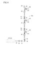
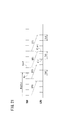
図17は、本変形例の光源装置(パルス光源装置、パルスレーザ装置)12Aの構成を示す図である。ファイバーレーザ装置としての光源装置12Aは、DFB半導体レーザ素子200、DFB半導体レーザ素子202、偏光ビームスプリッタ204、描画用光変調器としての電気光学素子206、この電気光学素子206の駆動回路206a、偏光ビームスプリッタ208、吸収体210、励起光源212、コンバイナ214、ファイバー光増幅器216、波長変換光学素子218、波長変換光学素子220、複数のレンズ素子GL、およびクロック発生器222aを含む制御回路(制御回路部)222を備える。   FIG. 17 is a diagram showing a configuration of a light source device (pulse light source device, pulse laser device) 12A of the present modification. A light source device 12A as a fiber laser device includes a DFB semiconductor laser element 200, a DFB semiconductor laser element 202, a polarization beam splitter 204, an electro-optic element 206 as a drawing optical modulator, a drive circuit 206a for the electro-optic element 206, a polarization A control circuit (control circuit) including a beam splitter 208, an absorber 210, an excitation light source 212, a combiner 214, a fiber optical amplifier 216, a wavelength conversion optical element 218, a wavelength conversion optical element 220, a plurality of lens elements GL, and a clock generator 222a. Part) 222.

DFB半導体レーザ素子(第1レーザ素子)200は、所定周波数Fsで俊鋭若しくは尖鋭のパルス状の種光(レーザ光)S1を発生し、DFB半導体レーザ素子(第2レーザ素子)202は、所定周波数Fsで緩慢(時間的にブロード)なパルス状の種光(レーザ光)S2を発生する。DFB半導体レーザ素子200が発生する種光S1と、DFB半導体レーザ素子202が発生する種光S2とは、エネルギーは略同一であるが、偏光状態が互いに異なり、ピーク強度は種光S1の方が強い。本変形例では、DFB半導体レーザ素子200が発生する種光S1の偏光状態をS偏光とし、DFB半導体レーザ素子202が発生する種光S2の偏光状態をP偏光として説明する。このDFB半導体レーザ素子200、202は、クロック発生器222aで生成されるクロック信号LTC(基本周波数Fs)に応答して、制御回路222の電気的な制御によって、発振周波数Fsで種光S1、S2を発光するように制御される。なお、このクロック信号LTCは、図16に示したカウンタ部CN1、CN3、CN5の各々に供給されるクロック信号CLKのベースとなるもので、クロック信号LTCをn分周(nは2以上の整数が好ましい)したものがクロック信号CLKとなる。また、クロック発生器222aは、クロック信号LTCの基本周波数Fsを±ΔFだけ調整する機能、すなわち、レーザ光LBのパルス発振の時間間隔を微調する機能も有する。これによって、例えば、スポット光の走査速度Vsが僅かに変動しても、基本周波数Fsを微調整することで、走査ラインLに渡って描画されるパターンの寸法(描画倍率)を精密に保つことができる。   The DFB semiconductor laser element (first laser element) 200 generates sharp or sharp pulsed seed light (laser light) S1 at a predetermined frequency Fs, and the DFB semiconductor laser element (second laser element) 202 has a predetermined frequency. Slow (time broad) pulsed seed light (laser light) S2 is generated at the frequency Fs. The seed light S1 generated by the DFB semiconductor laser element 200 and the seed light S2 generated by the DFB semiconductor laser element 202 have substantially the same energy, but have different polarization states, and the peak intensity is higher in the seed light S1. strong. In this modification, the polarization state of the seed light S1 generated by the DFB semiconductor laser element 200 is described as S-polarized light, and the polarization state of the seed light S2 generated by the DFB semiconductor laser element 202 is described as P-polarized light. The DFB semiconductor laser devices 200 and 202 respond to the clock signal LTC (fundamental frequency Fs) generated by the clock generator 222a and are electrically controlled by the control circuit 222 with the seed light S1 and S2 at the oscillation frequency Fs. Is controlled to emit light. The clock signal LTC is a base of the clock signal CLK supplied to each of the counter units CN1, CN3, and CN5 shown in FIG. 16, and the clock signal LTC is divided by n (n is an integer of 2 or more). Is preferably the clock signal CLK. The clock generator 222a also has a function of adjusting the basic frequency Fs of the clock signal LTC by ± ΔF, that is, a function of finely adjusting the time interval of pulse oscillation of the laser light LB. Thereby, for example, even if the scanning speed Vs of the spot light slightly fluctuates, the dimension (drawing magnification) of the pattern drawn over the scanning line L can be maintained precisely by finely adjusting the basic frequency Fs. Can do.

偏光ビームスプリッタ204は、S偏光の光を透過し、P偏光の光を反射するものであり、DFB半導体レーザ素子200が発生した種光S1と、DFB半導体レーザ素子202が発生した種光S2とを、電気光学素子206に照射する。詳しくは、偏光ビームスプリッタ204は、DFB半導体レーザ素子200が発生したS偏光の種光S1を透過することで種光S1を電気光学素子206に照射し、DFB半導体レーザ素子202が発生したP偏光の種光S2を反射することで種光S2を電気光学素子206に照射する。   The polarization beam splitter 204 transmits S-polarized light and reflects P-polarized light, and includes seed light S1 generated by the DFB semiconductor laser element 200 and seed light S2 generated by the DFB semiconductor laser element 202. Is applied to the electro-optic element 206. Specifically, the polarization beam splitter 204 transmits the S-polarized seed light S1 generated by the DFB semiconductor laser element 200 to irradiate the electro-optical element 206 with the seed light S1, and the P-polarized light generated by the DFB semiconductor laser element 202. The seed light S2 is reflected to irradiate the electro-optic element 206 with the seed light S2.

電気光学素子(変調部材)206は、種光S1、S2に対して透過性を有するものであり、例えば、電気光学変調器(EOM:Electro-Optic Modulator)が用いられる。EOMは、先の図16に示した描画ビット列データSdw(またはシリアルデータDLn)のOn/Off状態(H、またはL)に応答して、偏光ビームスプリッタ204を通ってきた種光S1、S2の偏光状態を駆動回路(駆動回路部)206aによって切り換えるものである。例えば、描画ビット列データSdw(またはDLn)がOff状態(L)のとき、電気光学素子206は、入射した種光S1またはS2の偏光状態を変えずにそのまま偏光ビームスプリッタ208に照射し、描画ビット列データSdw(またはDLn)がOn状態(H)のとき、電気光学素子206は入射した種光S1またはS2の偏光状態を変えて(偏光方向を90度変えて)偏光ビームスプリッタ208に照射する。したがって、電気光学素子206は、描画ビット列データSdw(またはDLn)がOn状態(H)のとき、S偏光の種光S1をP偏光の種光S1に変換し、P偏光の種光S2をS偏光の種光S2に変換する。   The electro-optic element (modulating member) 206 is transmissive to the seed lights S1 and S2, and for example, an electro-optic modulator (EOM: Electro-Optic Modulator) is used. The EOM responds to the On / Off state (H or L) of the drawing bit string data Sdw (or serial data DLn) shown in FIG. 16 and transmits the seed lights S1 and S2 that have passed through the polarization beam splitter 204. The polarization state is switched by a drive circuit (drive circuit unit) 206a. For example, when the drawing bit string data Sdw (or DLn) is in the Off state (L), the electro-optical element 206 directly irradiates the polarization beam splitter 208 without changing the polarization state of the incident seed light S1 or S2, and draws the drawing bit string. When the data Sdw (or DLn) is in the On state (H), the electro-optic element 206 changes the polarization state of the incident seed light S1 or S2 (changes the polarization direction by 90 degrees) and irradiates the polarization beam splitter 208. Therefore, when the drawing bit string data Sdw (or DLn) is in the On state (H), the electro-optic element 206 converts the S-polarized seed light S1 into the P-polarized seed light S1 and converts the P-polarized seed light S2 into S The light is converted into polarized seed light S2.

偏光ビームスプリッタ208は、P偏光の光は透過してレンズ素子GLを介してコンバイナ214に照射し、S偏光の光は反射させて吸収体210に照射する。励起光源212は励起光を発生し、該発生した励起光は、光ファイバー212aを介してコンバイナ214に導かれる。コンバイナ214は、偏光ビームスプリッタ208から照射された種光と励起光とを合成して、ファイバー光増幅器(光増幅器)216に出力する。ファイバー光増幅器216は、励起光によって励起されるレーザ媒質がドープされている。したがって、合成された種光および励起光が伝送するファイバー光増幅器216内では、励起光によってレーザ媒質が励起されることにより種光が増幅される。ファイバー光増幅器216内にドープされるレーザ媒質としては、エルビウム(Er)、イッテルビウム(Yb)、ツリウム(Tm)等の希土類元素が用いられる。この増幅された種光は、ファイバー光増幅器216の射出端216aから所定の発散角を伴って放射され、レンズ素子GLによって収斂またはコリメートされて波長変換光学素子218に入射する。   The polarization beam splitter 208 transmits the P-polarized light and irradiates the combiner 214 via the lens element GL, and reflects the S-polarized light to the absorber 210. The excitation light source 212 generates excitation light, and the generated excitation light is guided to the combiner 214 via the optical fiber 212a. The combiner 214 combines the seed light and the excitation light emitted from the polarization beam splitter 208 and outputs the combined light to the fiber optical amplifier (optical amplifier) 216. The fiber optical amplifier 216 is doped with a laser medium that is pumped by pumping light. Therefore, in the fiber optical amplifier 216 through which the synthesized seed light and pumping light are transmitted, the seed light is amplified by exciting the laser medium with the pumping light. As the laser medium doped in the fiber optical amplifier 216, rare earth elements such as erbium (Er), ytterbium (Yb), thulium (Tm) are used. The amplified seed light is emitted from the emission end 216a of the fiber optical amplifier 216 with a predetermined divergence angle, converged or collimated by the lens element GL, and enters the wavelength conversion optical element 218.

波長変換光学素子(第1の波長変換光学素子、波長変換光学部材)218は、第2高調波発生(Second Harmonic Generation:SHG)によって、入射した種光(波長λ)を、波長がλの1/2の第2高調波に変換する。波長変換光学素子218として、疑似位相整合(Quasi Phase Matching:QPM)結晶であるPPLN(Periodically Poled LiNbO3)結晶が好適に用いられる。なお、PPLT(Periodically Poled LiTaO3)結晶等を用いることも可能である。 A wavelength conversion optical element (first wavelength conversion optical element, wavelength conversion optical member) 218 is configured to generate incident seed light (wavelength λ) by using a second harmonic generation (SHG) and a wavelength of λ 1 Convert to / 2 second harmonic. As the wavelength conversion optical element 218, a PPLN (Periodically Poled LiNbO 3 ) crystal that is a quasi phase matching (QPM) crystal is preferably used. It is also possible to use a PPLT (Periodically Poled LiTaO 3 ) crystal or the like.

波長変換光学素子(第2の波長変換光学素子、波長変換光学部材)220は、波長変換光学素子218が変換した第2高調波(波長λ/2)と、波長変換光学素子218によって変換されずに残留した種光(波長λ)との和周波発生(Sum Frequency Generation:SFG)により、波長がλの1/3の第3高調波を発生する。この第3高調波が、370mm以下の波長帯域にピーク波長を有する紫外線光(レーザ光LB)となる。   The wavelength conversion optical element (second wavelength conversion optical element, wavelength conversion optical member) 220 is not converted by the wavelength conversion optical element 218 and the second harmonic (wavelength λ / 2) converted by the wavelength conversion optical element 218. The third harmonic wave whose wavelength is 1/3 of λ is generated by sum frequency generation (SFG) with the seed light (wavelength λ) remaining in the light source. This third harmonic becomes ultraviolet light (laser light LB) having a peak wavelength in a wavelength band of 370 mm or less.

以上のように、図16に示した描画データ生成回路から送出される描画ビット列データSdw(またはDLn)を、図17の電気光学素子206に印加する構成とした場合、描画ビット列データSdw(またはDLn)がOff状態(L)のとき、電気光学素子206は、入射した種光S1またはS2の偏光状態を変えずにそのまま偏光ビームスプリッタ208に照射するので、偏光ビームスプリッタ208を透過する種光は、DFB半導体レーザ素子202からの種光S2となる。したがって、光源装置12Aから最終的に出力されるレーザ光LBは、DFB半導体レーザ素子202からの種光S2と同じ発振プロファイル(時間特性)を有する。すなわち、レーザ光LBは、パルスのピーク強度が低く、時間的にブロードな鈍った特性となる。ファイバー光増幅器216は、そのようにピーク強度が低い種光S2に対する増幅効率が低いため、光源装置12Aから出力されるレーザ光LBは露光に必要なエネルギーまで増幅されない光となる。したがって、この場合は、露光という観点から見れば、実質的に光源装置12Aはレーザ光LBを射出していないのと同じ結果となる。但し、各走査ラインL1〜L6に沿ってパターン描画が行われない期間(非投射期間)では、種光S2由来の紫外域のレーザ光LBが僅かな強度であっても放射され続けるので、走査ラインL1〜L6が、長時間、基板P上の同じ位置に照射されるような状況(例えば、搬送系のトラブルによる基板Pの緊急停止等)が生じる場合は、光源装置12Aのレーザ光LBの射出窓に可動シャッターを設けて、射出窓を閉じるようにするとよい。   As described above, when the drawing bit string data Sdw (or DLn) sent from the drawing data generation circuit shown in FIG. 16 is applied to the electro-optic element 206 of FIG. 17, the drawing bit string data Sdw (or DLn) is applied. ) Is in the Off state (L), the electro-optical element 206 directly irradiates the polarization beam splitter 208 without changing the polarization state of the incident seed light S1 or S2, so that the seed light transmitted through the polarization beam splitter 208 is , Seed light S2 from the DFB semiconductor laser element 202. Therefore, the laser beam LB finally output from the light source device 12A has the same oscillation profile (time characteristic) as the seed light S2 from the DFB semiconductor laser element 202. That is, the laser beam LB has a low pulse peak intensity and has a broad and dull characteristic. Since the fiber optical amplifier 216 has low amplification efficiency with respect to the seed light S2 having such a low peak intensity, the laser light LB output from the light source device 12A becomes light that is not amplified to the energy required for exposure. Therefore, in this case, from the viewpoint of exposure, the light source device 12A has substantially the same result as not emitting the laser beam LB. However, in a period during which pattern drawing is not performed along each scanning line L1 to L6 (non-projection period), the laser beam LB in the ultraviolet region derived from the seed light S2 continues to be emitted even at a slight intensity. When a situation occurs such that the lines L1 to L6 are irradiated to the same position on the substrate P for a long time (for example, an emergency stop of the substrate P due to a trouble in the transport system), the laser beam LB of the light source device 12A A movable shutter may be provided on the exit window so that the exit window is closed.

一方、図17の電気光学素子206に印加する描画ビット列データSdw(またはDLn)がOn状態(H)のとき、電気光学素子206は、入射した種光S1またはS2の偏光状態を変えて偏光ビームスプリッタ208に照射するので、偏光ビームスプリッタ208を透過する種光は、DFB半導体レーザ素子200からの種光S1となる。したがって、光源装置12Aから出力されるレーザ光LBは、DFB半導体レーザ素子200からの種光S1に由来して生成されたものとなる。DFB半導体レーザ素子200からの種光S1はピーク強度が強いため、ファイバー光増幅器216によって効率的に増幅され、光源装置12Aから出力されるレーザ光LBは、基板Pの露光に必要なエネルギーを持つ。   On the other hand, when the drawing bit string data Sdw (or DLn) applied to the electro-optic element 206 in FIG. 17 is in the On state (H), the electro-optic element 206 changes the polarization state of the incident seed light S1 or S2 to change the polarization beam. Since the splitter 208 is irradiated, the seed light transmitted through the polarization beam splitter 208 becomes the seed light S 1 from the DFB semiconductor laser element 200. Therefore, the laser beam LB output from the light source device 12A is generated from the seed light S1 from the DFB semiconductor laser element 200. Since the seed light S1 from the DFB semiconductor laser element 200 has a strong peak intensity, the laser light LB efficiently amplified by the fiber optical amplifier 216 and output from the light source device 12A has energy necessary for exposure of the substrate P. .

このように、光源装置12A内に、描画用光変調器としての電気光学素子206を設けたので、上記第2の実施の形態において描画用光学素子150を制御するのと同様に、電気光学素子206を制御することで、上記第2の実施の形態と同様の効果を得ることができる。つまり、レーザ光LBが入射する描画ユニットUの描画データ(或いは図15、図16中の描画ビット列データSdw)に基づいて、電気光学素子206をオンオフにスイッチング(駆動)することで、初段のユニット選択用光学素子50に入射するレーザ光LBの強度、すなわち、基板P上に照射されるレーザ光LBの走査スポットの強度を描画すべきパターンに応じて変調させることができる。   As described above, since the electro-optic element 206 as the drawing optical modulator is provided in the light source device 12A, the electro-optic element is controlled in the same manner as the drawing optical element 150 is controlled in the second embodiment. By controlling 206, an effect similar to that of the second embodiment can be obtained. That is, by switching (driving) the electro-optic element 206 on and off based on the drawing data of the drawing unit U on which the laser beam LB is incident (or the drawing bit string data Sdw in FIGS. 15 and 16), the first unit The intensity of the laser beam LB incident on the selection optical element 50, that is, the intensity of the scanning spot of the laser beam LB irradiated on the substrate P can be modulated according to the pattern to be drawn.

なお、光源装置12Aは、DFB半導体レーザ素子202および偏光ビームスプリッタ204を有しない構造であってもよい。この場合は、電気光学素子206には、DFB半導体レーザ素子200からの種光S1のみが照射される。そして、描画データに基づいて電気光学素子206をオンオフにスイッチングすることで、初段のユニット選択用光学素子50に入射するレーザ光LBの強度を変調させることができる。しかしながら、この構成を採用すると、種光S1のファイバー光増幅器216への入射周期性が描画すべきパターンに応じて大きく乱される。すなわち、ファイバー光増幅器216にDFB半導体レーザ素子202からの種光S1が入射しない状態が続いた後に、ファイバー光増幅器216に種光S1が入射すると、入射直後の種光S1は通常のときよりも大きな増幅率で増幅され、ファイバー光増幅器216からは、規定以上の大きな強度を持つビームが発生するという問題がある。そこで、本変形例では、好ましい態様として、ファイバー光増幅器216に種光S1が入射しない期間に、DFB半導体レーザ素子202からの種光S2(ピーク強度が低いブロードなパルス光)をファイバー光増幅器216に入射することで、このような問題を解決している。   The light source device 12A may have a structure that does not include the DFB semiconductor laser element 202 and the polarization beam splitter 204. In this case, the electro-optic element 206 is irradiated with only the seed light S1 from the DFB semiconductor laser element 200. The intensity of the laser beam LB incident on the first-stage unit selection optical element 50 can be modulated by switching the electro-optic element 206 on and off based on the drawing data. However, when this configuration is employed, the periodicity of incidence of the seed light S1 on the fiber optical amplifier 216 is greatly disturbed according to the pattern to be drawn. That is, after the seed light S1 from the DFB semiconductor laser element 202 is not incident on the fiber optical amplifier 216 and then the seed light S1 is incident on the fiber optical amplifier 216, the seed light S1 immediately after the incident is more than normal. There is a problem that a beam having a large intensity exceeding a specified level is generated from the fiber optical amplifier 216 with a large amplification factor. Therefore, in this modified example, as a preferred embodiment, the seed light S2 (broad pulse light with low peak intensity) from the DFB semiconductor laser element 202 is used as the fiber optical amplifier 216 during the period when the seed light S1 is not incident on the fiber optical amplifier 216. This problem is solved by being incident on.

また、電気光学素子206をスイッチングするようにしたが、描画データ(描画ビット列データSdw)に基づいて、DFB半導体レーザ素子200、202を駆動するようにしてもよい。つまり、制御回路222は、描画データ(描画ビット列データSdw、またはDLn)に基づいて、DFB半導体レーザ素子200、202を制御して、基本周波数Fsでパルス状に発振する種光S1、S2を選択的(択一的)に発生させる。この場合は、偏光ビームスプリッタ204、208、電気光学素子206、および吸収体210は不要となり、DFB半導体レーザ素子200、202のいずれか一方から選択的にパルス発振される種光S1、S2の一方が、直接コンバイナ214に入射する。このとき、制御回路222は、DFB半導体レーザ素子200からの種光S1と、DFB半導体レーザ素子202からの種光S2とが同時にファイバー光増幅器216に入射しないように、各DFB半導体レーザ素子200、202の駆動を制御する。すなわち、基板Pにレーザ光LBを照射する場合は、種光S1のみがファイバー光増幅器216に入射するようにDFB半導体レーザ素子200を制御する。また、基板Pにレーザ光LBを照射しない場合には、種光S2のみがファイバー光増幅器216に入射するようにDFB半導体レーザ素子202を制御する。この基板Pにレーザ光LBを照射するか否かは、描画データ(描画ビット列データSdwのHまたはL)に基づいて決定される。   Further, although the electro-optic element 206 is switched, the DFB semiconductor laser elements 200 and 202 may be driven based on the drawing data (drawing bit string data Sdw). That is, the control circuit 222 controls the DFB semiconductor laser elements 200 and 202 based on the drawing data (drawing bit string data Sdw or DLn), and selects the seed lights S1 and S2 that oscillate in a pulse shape at the fundamental frequency Fs. (Alternatively) to generate. In this case, the polarizing beam splitters 204 and 208, the electro-optical element 206, and the absorber 210 are not necessary, and one of the seed lights S1 and S2 that are selectively pulse-oscillated from either one of the DFB semiconductor laser elements 200 and 202. Directly enters the combiner 214. At this time, the control circuit 222 prevents the seed light S1 from the DFB semiconductor laser element 200 and the seed light S2 from the DFB semiconductor laser element 202 from entering the fiber optical amplifier 216 at the same time. The driving of 202 is controlled. That is, when the substrate P is irradiated with the laser beam LB, the DFB semiconductor laser element 200 is controlled so that only the seed light S1 enters the fiber optical amplifier 216. When the substrate P is not irradiated with the laser light LB, the DFB semiconductor laser element 202 is controlled so that only the seed light S2 enters the fiber optical amplifier 216. Whether or not the substrate P is irradiated with the laser beam LB is determined based on the drawing data (H or L of the drawing bit string data Sdw).

このように、本変形例においても、音響光学変調素子の数を減らすことができ、コストが低廉になる。   Thus, also in this modification, the number of acousto-optic modulation elements can be reduced and the cost is reduced.

なお、本変形例の光源装置12A、12Bを、上記第1の実施の形態の光源装置12a、12bに用いてもよい。この場合は、光源装置12A、12Bから出力されるDFB半導体レーザ素子200からの種光S1の出力タイミングと、各描画ユニットU1〜U6の描画用光学素子106のスイッチングとを、描画データ(描画ビット列データSdw)に基づいて制御してもよい。   In addition, you may use light source device 12A, 12B of this modification for the light source device 12a, 12b of the said 1st Embodiment. In this case, the output timing of the seed light S1 from the DFB semiconductor laser element 200 output from the light source devices 12A and 12B and the switching of the drawing optical element 106 of each drawing unit U1 to U6 are set as drawing data (drawing bit string). Control may be performed based on the data Sdw).

[第3の実施の形態]
次に、図18を参照して、第3の実施の形態について説明するが、第3の実施の形態では、第2の実施の形態の変形例で説明した光源装置12A(図17参照)、12Bを用いることを前提とする。但し、第3の実施の形態に適するように、図17の光源装置12Aの制御回路222内のクロック発生器222aは、図18に示す描画制御用の制御ユニット(制御回路500)からの倍率補正情報CMgに応じて、クロック信号LTCの時間間隔を部分的(離散的)に伸縮する機能を備える。同様に、光源装置12Bの制御回路222内のクロック発生器222aも、倍率補正情報CMgに応じて、クロック信号LTCの時間間隔を部分的(離散的)に伸縮する機能を備える。なお、光源装置12B、光導入光学系40b、および、描画ユニットU2、U4、U6の動作は、光源装置12A、光導入光学系40a、および、描画ユニットU1、U3、U5の動作と同様なので、光源装置12B、光導入光学系40b、および、描画ユニットU2、U4、U6の動作については説明を省略する。また、上記第2の実施の形態の変形例と同一の構成については同様の符号を付したり、図示を省略したりし、異なる部分のみ説明する。
[Third Embodiment]
Next, the third embodiment will be described with reference to FIG. 18. In the third embodiment, the light source device 12A (see FIG. 17) described in the modification of the second embodiment, It is assumed that 12B is used. However, as suitable for the third embodiment, the clock generator 222a in the control circuit 222 of the light source device 12A in FIG. 17 is corrected for the magnification from the control unit (control circuit 500) for drawing control shown in FIG. In accordance with the information CMg, the clock signal LTC has a function of expanding or contracting partially (discretely) the time interval of the clock signal LTC. Similarly, the clock generator 222a in the control circuit 222 of the light source device 12B also has a function of expanding or contracting the time interval of the clock signal LTC partially (discretely) according to the magnification correction information CMg. The operations of the light source device 12B, the light introduction optical system 40b, and the drawing units U2, U4, U6 are the same as the operations of the light source device 12A, the light introduction optical system 40a, and the drawing units U1, U3, U5. Description of the operations of the light source device 12B, the light introducing optical system 40b, and the drawing units U2, U4, and U6 will be omitted. Further, the same components as those of the modification of the second embodiment are denoted by the same reference numerals or the illustration thereof is omitted, and only different portions will be described.

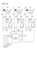
図18において、1つの光源装置12Aからのレーザ光(ビーム)LBは、先の図12、図13の構成と同様に、ユニット選択用光学素子50、58、66を介して、それぞれ3つの描画ユニットU1、U3、U5に供給される。ユニット選択用光学素子50、58、66の各々は、図14、図15で説明した描画イネーブル(On)信号SP1、SP3、SP5に応答して択一的にレーザ光LBを偏向(スイッチング)し、描画ユニットU1、U3、U5のいずれか1つにレーザ光LBを導く。なお、先に説明したように、各走査ラインに沿ってパターン描画が行われない期間(非投射期間)で、種光S2由来の紫外域のレーザ光LBが僅かな強度であっても放射され続け、各走査ラインが長時間に渡って基板P上の同じ位置に照射されるような状況が生じる場合を考慮して、光源装置12Aのレーザ光LBの射出窓には可動シャッターSSTが設けられる。   In FIG. 18, three laser beams (beams) LB from one light source device 12A are drawn via the unit selecting optical elements 50, 58, and 66, respectively, in the same manner as the configuration of FIGS. Supplied to units U1, U3, U5. Each of the unit selecting optical elements 50, 58 and 66 selectively deflects (switches) the laser light LB in response to the drawing enable (On) signals SP1, SP3 and SP5 described with reference to FIGS. The laser beam LB is guided to any one of the drawing units U1, U3, and U5. Note that, as described above, the ultraviolet laser beam LB derived from the seed light S2 is radiated even during a period in which pattern drawing is not performed along each scanning line (non-projection period). Subsequently, in consideration of a situation where each scanning line is irradiated to the same position on the substrate P for a long time, a movable shutter SST is provided at the exit window of the laser beam LB of the light source device 12A. .

図14で示したように、各描画ユニットU1、U3、U5の原点センサーSz1、Sz3、Sz5からの原点信号ZP1、ZP3、ZP5は、描画ユニットU1、U3、U5ごとの描画データを生成する生成回路(描画データ生成回路)501、503、505に供給される。生成回路501は、図16中のゲート部GT1、メモリ部BM1、カウンタ部CN1等を含み、カウンタ部CN1は光源装置12Aの制御回路222(クロック発生器222a)から出力されるクロック信号LTCをベースに作られるクロック信号CLK1を計数するように構成される。   As shown in FIG. 14, the origin signals ZP1, ZP3, ZP5 from the origin sensors Sz1, Sz3, Sz5 of the respective drawing units U1, U3, U5 are generated to generate drawing data for each of the drawing units U1, U3, U5. This is supplied to circuits (drawing data generation circuits) 501, 503, and 505. The generation circuit 501 includes a gate unit GT1, a memory unit BM1, a counter unit CN1, and the like in FIG. 16. The counter unit CN1 is based on a clock signal LTC output from the control circuit 222 (clock generator 222a) of the light source device 12A. Is configured to count the clock signal CLK1 produced.

同様に、生成回路503は、図16中のゲート部GT3、メモリ部BM3、カウンタ部CN3等を含み、カウンタ部CN3はクロック信号LTCをベースに作られるクロック信号CLK3を計数するように構成され、生成回路505は、図16中のゲート部GT5、メモリ部BM5、カウンタ部CN5等を含み、カウンタ部CN5はクロック信号LTCをベースに作られるクロック信号CLK5を計数するように構成される。   Similarly, the generation circuit 503 includes the gate unit GT3, the memory unit BM3, the counter unit CN3, and the like in FIG. 16, and the counter unit CN3 is configured to count the clock signal CLK3 generated based on the clock signal LTC. The generation circuit 505 includes the gate unit GT5, the memory unit BM5, the counter unit CN5, and the like in FIG. 16, and the counter unit CN5 is configured to count the clock signal CLK5 generated based on the clock signal LTC.

それらのクロック信号CLK1、CLK3、CLK5は、各生成回路501、503、505と光源装置12Aとの間のインターフェースとして機能する制御回路500によって、クロック信号LTCを1/n(nは2以上の整数)分周して作られる。そのクロック信号CLK1、CLK3、CLK5の各カウンタ部CN1、CN3、CN5への供給は、描画イネーブル(On)信号SP1、SP3、SP5(図15参照)に応答して、いずれか1つに制限される。すなわち、描画イネーブル信号SP1がOn(H)のときは、クロック信号LTCを1/n分周したクロック信号CLK1のみがカウンタ部CN1に供給され、描画イネーブル信号SP3がOn(H)のときは、クロック信号LTCを1/n分周したクロック信号CLK3のみがカウンタ部CN3に供給され、描画イネーブル信号SP5がOn(H)のときは、クロック信号LTCを1/n分周したクロック信号CLK5のみがカウンタ部CN5に供給される。   These clock signals CLK1, CLK3, and CLK5 are converted to 1 / n (n is an integer of 2 or more) by the control circuit 500 functioning as an interface between the generation circuits 501, 503, and 505 and the light source device 12A. ) Made by dividing. The supply of the clock signals CLK1, CLK3, and CLK5 to each counter unit CN1, CN3, and CN5 is limited to one in response to the drawing enable (On) signals SP1, SP3, and SP5 (see FIG. 15). The That is, when the drawing enable signal SP1 is On (H), only the clock signal CLK1 obtained by dividing the clock signal LTC by 1 / n is supplied to the counter unit CN1, and when the drawing enable signal SP3 is On (H), Only the clock signal CLK3 obtained by dividing the clock signal LTC by 1 / n is supplied to the counter unit CN3. When the drawing enable signal SP5 is On (H), only the clock signal CLK5 obtained by dividing the clock signal LTC by 1 / n is used. It is supplied to the counter unit CN5.

これによって、各生成回路501、503、505の各々から順番に出力されるシリアルデータDL1、DL3、DL5はそれぞれゲート部GT1、GT3、GT5を介して、制御回路500内に設けられた3入力のOR回路GT4によって加算され、描画ビット列データSdwとなって光源装置12A内の電気光学素子206に供給される。なお、生成回路501、503、505、および、制御回路500は、制御部18の一部を構成する。   As a result, serial data DL1, DL3, DL5 output in order from each of the generation circuits 501, 503, 505 are three-inputs provided in the control circuit 500 via the gate portions GT1, GT3, GT5, respectively. The sum is added by the OR circuit GT4 and supplied as drawing bit string data Sdw to the electro-optical element 206 in the light source device 12A. The generation circuits 501, 503, and 505 and the control circuit 500 constitute a part of the control unit 18.

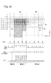
以上の構成は、基本的に図17を用いて説明した光源装置12Aの利用法と同じであるが、本実施の形態では、3つの描画ユニットU1、U3、U5の各々の走査ライン(描画ライン)L1、L3、L5によって描画されるパターンのスポット走査方向(Y方向)の描画倍率を、個別に微調整する機能を設ける。その機能のために、本実施の形態では、描画ユニットU1、U3、U5毎に、描画倍率の補正量に関する情報mg1、mg3、mg5を一時的に記憶するメモリ部BM1a、BM3a、BM5aが設けられる。このメモリ部BM1a、BM3a、BM5aは、図18では独立したものとして図示したが、生成回路501、503、505の各々に設けられたメモリ部BM1、BM3、BM5の一部としてもよい。この補正量に関する情報mg1、mg3、mg5も描画情報の一部を構成する。   The above configuration is basically the same as the method of using the light source device 12A described with reference to FIG. 17, but in this embodiment, each scanning line (drawing line) of each of the three drawing units U1, U3, and U5. ) A function for finely adjusting the drawing magnification in the spot scanning direction (Y direction) of the pattern drawn by L1, L3, and L5 individually is provided. For this function, in the present embodiment, memory units BM1a, BM3a, and BM5a that temporarily store information mg1, mg3, and mg5 related to the drawing magnification correction amount are provided for each of the drawing units U1, U3, and U5. . The memory units BM1a, BM3a, and BM5a are illustrated as independent in FIG. 18, but may be part of the memory units BM1, BM3, and BM5 provided in the generation circuits 501, 503, and 505, respectively. The information mg1, mg3, and mg5 regarding the correction amount also constitute part of the drawing information.

補正量に関する情報mg1、mg3、mg5は、例えば、各走査ラインL1、L3、L5によって描画されるパターンのY方向の寸法を、どれ位の比率で伸縮させるかのレート(ppm)に対応したものである。一例として、各走査ラインL1、L3、L5によって描画可能なY方向の領域の長さを30mmとした場合、それを±200ppm(±6μmに相当)だけ伸縮させたい場合、情報mg1、mg3、mg5には、±200という数値が設定される。なお、情報mg1、mg3、mg5は、レートではなく直接的な伸縮量(±ρμm)で設定しても構わない。また、情報mg1、mg3、mg5は、走査ラインL1、L3、L5の各々に沿った1ライン分の描画データ(シリアルデータ)毎に逐次設定し直してもよいし、複数ライン分の描画データ(シリアルデータ)の送出毎に設定し直してもよい。このように、本実施の形態では、基板PをX方向(長尺方向)に送りつつ、走査ラインL1、L3、L5の各々に沿ってパターン描画が行われている間に、動的にY方向の描画倍率を変えることが可能となり、基板Pの変形や面内歪が判る場合には、それに起因した描画位置精度の劣化を抑えることができる。さらに重ね合わせ露光の際には、既に形成された下地のパターンの変形に対応して重ね精度を大幅に向上させることができる。   The information regarding correction amounts mg1, mg3, and mg5 corresponds to, for example, the rate (ppm) of how much the dimension in the Y direction of the pattern drawn by each scanning line L1, L3, and L5 is expanded or contracted. It is. As an example, if the length of the region in the Y direction that can be drawn by each of the scanning lines L1, L3, and L5 is 30 mm, the information mg1, mg3, and mg5 can be expanded and contracted by ± 200 ppm (corresponding to ± 6 μm). Is set to a numerical value of ± 200. The information mg1, mg3, and mg5 may be set not by the rate but by a direct expansion / contraction amount (± ρμm). Further, the information mg1, mg3, and mg5 may be sequentially reset for each drawing data (serial data) for one line along each of the scanning lines L1, L3, and L5, or drawing data for a plurality of lines ( It may be reset every time serial data is transmitted. Thus, in the present embodiment, while the pattern is drawn along each of the scanning lines L1, L3, and L5 while feeding the substrate P in the X direction (longitudinal direction), the Y is dynamically changed. The drawing magnification in the direction can be changed, and when the deformation or in-plane distortion of the substrate P is known, it is possible to suppress the deterioration of the drawing position accuracy due to the deformation. Further, in the overlay exposure, the overlay accuracy can be greatly improved in response to the deformation of the base pattern already formed.

図19は、図18に示した描画装置のうち、代表して描画ユニットU1による標準的なパターン描画の際の各部の信号状態とレーザ光LBの発振状態とのタイムチャートを示す。図19において、2次元のマトリックスGmは、描画すべきパターンPPの描画マップ(ビットマップ)を示し、基板P上での1グリッド(1画素単位)は、例えばY方向の寸法Pyを3μm、X方向の寸法Pxを3μmに設定される。また、図19において、矢印で示すL1−1、L1−2、L1−3、・・・L1−6は、基板PのX方向の移動(長尺方向の副走査)に伴って、走査ラインL1によって順次描画される描画ラインを示し、各走査ラインL1−1、L1−2、L1−3、・・・L1−6のX方向の間隔は、例えば1画素単位の寸法Px(3μm)の1/2となるように、基板Pの搬送速度が設定される。   FIG. 19 shows a time chart of the signal state of each part and the oscillation state of the laser beam LB as a representative of the drawing apparatus shown in FIG. 18 at the time of standard pattern drawing by the drawing unit U1. In FIG. 19, a two-dimensional matrix Gm shows a drawing map (bitmap) of a pattern PP to be drawn, and one grid (one pixel unit) on the substrate P has a dimension Py in the Y direction of 3 μm, for example, The direction dimension Px is set to 3 μm. In FIG. 19, L1-1, L1-2, L1-3,... L1-6 indicated by arrows indicate scanning lines as the substrate P moves in the X direction (long-direction sub-scanning). The drawing lines sequentially drawn by L1 are shown. The interval in the X direction of each scanning line L1-1, L1-2, L1-3,... L1-6 is, for example, a size Px (3 μm) in units of one pixel. The conveyance speed of the substrate P is set so as to be ½.

さらに、基板P上に投射されるスポット光SPのXY方向の寸法(スポットサイズ)は、1画素単位と同程度か、それよりも少し大きめとする。よって、スポット光SPのサイズは、実効的な直径(ガウス分布の1/e2の幅、またはピーク強度の半値全幅)として、3〜4μm程度に設定され、走査ラインLに沿ってスポット光SPを連続的に投射する際は、例えばスポット光の実効的な直径の1/2でオーバーラップするように、レーザ光LBの発振周波数Fs(パルス時間間隔)とポリゴンミラー116によるスポット光SPの走査速度Vsとが設定されている。すなわち、光源装置12A内の偏光ビームスプリッタ208から射出される種光をビームLse(図18)とすると、この種光ビームLseは、制御回路222(クロック発生器222a)から出力されるクロック信号LTCの各クロックパルスに応答して図19のように射出される。 Furthermore, the dimension (spot size) of the spot light SP projected on the substrate P in the XY direction is approximately the same as one pixel unit or slightly larger. Therefore, the size of the spot light SP is set to about 3 to 4 μm as an effective diameter (width of 1 / e 2 of Gaussian distribution or full width at half maximum of peak intensity), and the spot light SP along the scanning line L is set. Is continuously scanned, for example, the oscillation frequency Fs (pulse time interval) of the laser beam LB and the scanning of the spot beam SP by the polygon mirror 116 so as to overlap each other by 1/2 of the effective diameter of the spot beam. Speed Vs is set. That is, if the seed light emitted from the polarization beam splitter 208 in the light source device 12A is a beam Lse (FIG. 18), the seed light beam Lse is a clock signal LTC output from the control circuit 222 (clock generator 222a). In response to each clock pulse of FIG.

そのクロック信号LTCと、図18中の生成回路501内のカウンタ部CN1に供給されるクロック信号CLK1とは、1:2の周波数比に設定され、クロック信号LTCが100MHzの場合、図18中の制御回路500の1/2分周器によって、クロック信号CLK1は50MHzに設定される。なお、クロック信号LTCとクロック信号CLK1の周波数比は整数倍であればよく、例えばクロック信号CLK1の設定周波数を半分の25MHzに落とすと共に、スポット光の走査速度Vsも半分に落とすように設定してもよい。   The clock signal LTC and the clock signal CLK1 supplied to the counter unit CN1 in the generation circuit 501 in FIG. 18 are set to a frequency ratio of 1: 2, and when the clock signal LTC is 100 MHz, The clock signal CLK1 is set to 50 MHz by the 1/2 frequency divider of the control circuit 500. The frequency ratio between the clock signal LTC and the clock signal CLK1 only needs to be an integral multiple. For example, the setting frequency of the clock signal CLK1 is set to be lowered to 25 MHz, and the scanning speed Vs of the spot light is also reduced to half. Also good.

図19に示す描画ビット列データSdwは、生成回路501から出力されるシリアルデータDL1に相当し、ここでは、例えばパターンPPの走査ラインL1−2上のパターンに対応している。光源装置12A内の電気光学素子206は、描画ビット列データSdwに応答して偏光状態を切り換えるので、種光ビームLseは、描画ビット列データSdwがOn状態(「H」)の間は、図17中のDFB半導体レーザ素子200からの種光S1によって生成され、描画ビット列データSdwがOff状態(「L」)の間は、図17中のDFB半導体レーザ素子202からの種光S2によって生成される。   The drawing bit string data Sdw shown in FIG. 19 corresponds to the serial data DL1 output from the generation circuit 501, and corresponds to, for example, a pattern on the scanning line L1-2 of the pattern PP. Since the electro-optic element 206 in the light source device 12A switches the polarization state in response to the drawing bit string data Sdw, the seed light beam Lse is shown in FIG. 17 while the drawing bit string data Sdw is in the On state (“H”). 17 is generated by the seed light S1 from the DFB semiconductor laser element 200, and is generated by the seed light S2 from the DFB semiconductor laser element 202 in FIG. 17 while the drawing bit string data Sdw is in the off state (“L”).

なお、光源装置12Aの制御回路222内に、描画ビット列データSdwがOn状態(「H」)の間は、クロック信号LTCに応答してDFB半導体レーザ素子200から種光S1(俊鋭なパルス光)を発生させ、描画ビット列データSdwがOff状態(「L」)の間は、クロック信号LTCに応答してDFB半導体レーザ素子202から種光S2(ブロードなパルス光)を発生させるような駆動回路が設けられる場合は、図17、図18中に示した電気光学素子206、図17中に示した偏光ビームスプリッタ208、吸収体210は省略できる。   In the control circuit 222 of the light source device 12A, while the drawing bit string data Sdw is in the On state (“H”), the seed light S1 (sharp pulse light) is transmitted from the DFB semiconductor laser element 200 in response to the clock signal LTC. ), And the drawing bit string data Sdw is in the off state (“L”), the drive circuit generates seed light S2 (broad pulse light) from the DFB semiconductor laser element 202 in response to the clock signal LTC. 17 can be omitted, the electro-optic element 206 shown in FIGS. 17 and 18, the polarizing beam splitter 208 and the absorber 210 shown in FIG. 17 can be omitted.

このように、種光ビームLseの各パルス光は、図17に示したクロック発生器222aで生成されるクロック信号LTCの各クロックパルスに応答して出力されるので、本実施の形態では、クロック発生器222a内に、クロック信号LTCのパルス間の時間(周期)を部分的に増減するための回路構成を設ける。その回路構成には、クロック信号LTCの源となる基準(標準)クロック発生器と、分周カウンタ回路と、可変遅延回路等が設けられる。   As described above, each pulse light of the seed light beam Lse is output in response to each clock pulse of the clock signal LTC generated by the clock generator 222a shown in FIG. A circuit configuration for partially increasing or decreasing the time (cycle) between pulses of the clock signal LTC is provided in the generator 222a. The circuit configuration includes a reference (standard) clock generator that is a source of the clock signal LTC, a frequency division counter circuit, a variable delay circuit, and the like.

図20は、クロック発生器222a内の基準クロック発生器からの基準クロック信号TC0と、クロック信号LTCとの関係を示すタイムチャートであり、図17、図18中に示した倍率補正情報CMgに基づく補正が行われない状態を示す。クロック発生器222a内の可変遅延回路は、常に一定周波数Fs(一定の時間Td0)で生成される基準クロック信号TC0を、プリセット値に応じた時間DT0だけ遅延させて、クロック信号LTCとして出力する。したがって、例えば、基準クロック信号TC0が100MHz(Td0=10nS)であれば、プリセット値(遅延時間DT0)に変化が生じない限り、クロック信号LTCも100MHz(Td0=10nS)で生成され続けられる。   FIG. 20 is a time chart showing the relationship between the reference clock signal TC0 from the reference clock generator in the clock generator 222a and the clock signal LTC, and is based on the magnification correction information CMg shown in FIGS. Indicates a state in which no correction is performed. The variable delay circuit in the clock generator 222a always delays the reference clock signal TC0 generated at the constant frequency Fs (constant time Td0) by the time DT0 corresponding to the preset value, and outputs it as the clock signal LTC. Therefore, for example, if the reference clock signal TC0 is 100 MHz (Td0 = 10 nS), the clock signal LTC is also continuously generated at 100 MHz (Td0 = 10 nS) as long as there is no change in the preset value (delay time DT0).

そこで、クロック発生器222a内の分周カウンタ回路によって、基準クロック信号TC0を計数し、その計数値が所定値Nvに達したら、可変遅延回路に設定されるプリセット値を一定量だけ変化させる構成にする。その様子を、図21のタイムチャートにより説明する。図21において、基準クロック信号TC0が分周カウンタ回路によってからNvまでカウントされるまで、可変遅延回路に設定されるプリセット値は遅延時間DT0である。その後、基準クロック信号TC0の1つのクロックパルスKnによって、分周カウンタ回路がNvまで計数すると、可変遅延回路に設定されるプリセット値は、直ちに遅延時間DT1に変更される。したがって、基準クロック信号TC0のクロックパルスKnの次に発生するクロックパルスKn+1以降に生成されるクロック信号LTCの各クロックパルス(K’n+1以降)は、一律に遅延時間DT1で生成される。   Therefore, the reference clock signal TC0 is counted by the frequency dividing counter circuit in the clock generator 222a, and when the count value reaches the predetermined value Nv, the preset value set in the variable delay circuit is changed by a certain amount. To do. This will be described with reference to the time chart of FIG. In FIG. 21, until the reference clock signal TC0 is counted from the frequency dividing counter circuit to Nv, the preset value set in the variable delay circuit is the delay time DT0. Thereafter, when the frequency division counter circuit counts up to Nv by one clock pulse Kn of the reference clock signal TC0, the preset value set in the variable delay circuit is immediately changed to the delay time DT1. Therefore, each clock pulse (after K′n + 1) of the clock signal LTC generated after the clock pulse Kn + 1 generated after the clock pulse Kn of the reference clock signal TC0 is uniformly generated with the delay time DT1.

これによって、可変遅延回路に設定されるプリセット値を一定量変化させたときだけ、すなわち、クロック信号LTCのクロックパルスK’nとクロックパルスK’n+1との間だけが時間間隔Td1に変化し、それ以降のクロック信号LTCのクロックパルスの時間間隔はTd0となる。図21では、遅延時間DT1を遅延時間DT0よりも増加させて、クロック信号LTCの2つのクロックパルス間の時間をTd0よりも増加させたが、減少させることも同様に可能である。なお、分周カウンタ回路は、基準クロック信号TC0をNvまでカウントしたら零リセットされて、再びNvまでの計数を始める。   Thereby, only when the preset value set in the variable delay circuit is changed by a certain amount, that is, only between the clock pulse K′n and the clock pulse K′n + 1 of the clock signal LTC changes to the time interval Td1, Subsequent clock pulse time intervals of the clock signal LTC are Td0. In FIG. 21, the delay time DT1 is increased from the delay time DT0 and the time between two clock pulses of the clock signal LTC is increased from Td0. However, it is also possible to decrease the time. The frequency dividing counter circuit is reset to zero when the reference clock signal TC0 is counted up to Nv, and starts counting up to Nv again.

可変遅延回路に設定されるプリセット値の初期値を遅延時間DT0、遅延時間の変化量を±ΔDh、分周カウンタ回路が零リセットされる回数をNzとし、分周カウンタ回路がNvまで計数する度(零リセットされる度)に可変遅延回路に順次設定されるプリセット値の遅延時間をDTmとすると、遅延時間DTmは、DTm=DT0+Nz・(±ΔDh)、の関係に設定される。したがって、図21のように、零リセットの回数Nzが1(m=1)の間に設定される遅延時間DT1は、DTm=DT1=DT0±ΔDhとなり、次の零リセット(Nz=2、m=2)が発生した後に設定される遅延時間DT2は、DTm=DT2=DT0+2・(±ΔDh)となる。したがって、遅延時間の変化量±ΔDhは、クロック信号LTCのクロックパルスK’nとクロックパルスK’n+1との間の時間Td1の基準時間Td0からの差分に対応する。   The initial value of the preset value set in the variable delay circuit is the delay time DT0, the amount of change in the delay time is ± ΔDh, the number of times the frequency division counter circuit is reset to zero is Nz, and the frequency division counter circuit counts up to Nv If the delay time of preset values sequentially set in the variable delay circuit every time (zero reset) is DTm, the delay time DTm is set to a relationship of DTm = DT0 + Nz · (± ΔDh). Therefore, as shown in FIG. 21, the delay time DT1 set while the number of zero resets Nz is 1 (m = 1) is DTm = DT1 = DT0 ± ΔDh, and the next zero reset (Nz = 2, m = 2) occurs, the delay time DT2 set is DTm = DT2 = DT0 + 2 · (± ΔDh). Accordingly, the delay time variation ± ΔDh corresponds to the difference from the reference time Td0 of the time Td1 between the clock pulse K′n and the clock pulse K′n + 1 of the clock signal LTC.

以上のように、クロック信号LTCの特定の2つのクロックパルス間で時間間隔を変化させる動作は、分周カウンタ回路に設定される所定値Nvに応じて、1つの走査ライン(L1〜L6)の全長のうちの複数箇所で離散的に実施される。その様子を、図22に示す。図22は、走査ラインL1の全長に渡って、分周カウンタ回路の計数値が所定値Nvに達する度に零リセットされる複数の位置を補正点CPPとして表したものである。その補正点CPPの各々では、クロック信号LTCの特定の2つのクロックパルス間だけが、時間Td0に対して±ΔDhだけ時間伸縮される。   As described above, the operation of changing the time interval between two specific clock pulses of the clock signal LTC is performed on one scan line (L1 to L6) according to the predetermined value Nv set in the frequency division counter circuit. It is carried out discretely at a plurality of points in the total length. This is shown in FIG. FIG. 22 shows a plurality of positions that are reset to zero each time the count value of the frequency division counter circuit reaches a predetermined value Nv over the entire length of the scanning line L1, as correction points CPP. At each of the correction points CPP, only the interval between two specific clock pulses of the clock signal LTC is expanded or contracted by ± ΔDh with respect to the time Td0.

そこで、基準クロック信号TC0を100MHz(Td0=10nS)、スポット光の主走査方向の実効的なサイズを3μm、走査ラインL1(L2〜L6も同様)の長さを30mmとし、レーザ光LBの2つの連続したパルス光によって基板Pに投射されるスポット光が主走査方向に半分程度(1.5μm)オーバーラップして描画されるものとすると、走査ラインL1の長さに渡って生成される基準クロック信号TC0のクロック数は20000個となる。また、遅延時間の変化量ΔDhは、基準の時間間隔Td0に対して十分に小さく、例えば2%程度に設定されるものとする。この条件のもとで、走査ラインL1に沿って描画されるパターンを、150ppmだけ主走査方向(Y方向)に伸縮させる場合、走査ラインL1の長さ30mmの150ppmは4.5μmに相当する。これらの描画倍率のレート150ppm、或いは実寸長4.5μmに関する情報は、図18中のメモリ部BM1aに情報mg1として保存される。   Therefore, the reference clock signal TC0 is 100 MHz (Td0 = 10 nS), the effective size of the spot light in the main scanning direction is 3 μm, the length of the scanning line L1 (same for L2 to L6) is 30 mm, and 2 of the laser light LB Assuming that spot light projected onto the substrate P by two continuous pulse lights is drawn with an overlap of about half (1.5 μm) in the main scanning direction, a reference generated over the length of the scanning line L1. The number of clocks of the clock signal TC0 is 20000. The delay time change amount ΔDh is sufficiently small with respect to the reference time interval Td0, and is set to, for example, about 2%. Under this condition, when a pattern drawn along the scanning line L1 is expanded or contracted in the main scanning direction (Y direction) by 150 ppm, 150 ppm of the scanning line L1 having a length of 30 mm corresponds to 4.5 μm. Information regarding the drawing magnification rate of 150 ppm or the actual size length of 4.5 μm is stored as information mg1 in the memory unit BM1a in FIG.

したがって、クロック信号LTCの20000個のクロックパルス列のうち、時間Td0に対してΔDhだけ時間伸縮させる補正点CPP(図22)の個数は、4.5μm/(1.5μm×2%)=150となり、図22に示した分周カウンタ回路に設定される最大の所定値Nvは、20000/150より、約133となる。   Accordingly, among 20000 clock pulse trains of the clock signal LTC, the number of correction points CPP (FIG. 22) for time expansion / contraction by ΔDh with respect to time Td0 is 4.5 μm / (1.5 μm × 2%) = 150. The maximum predetermined value Nv set in the frequency division counter circuit shown in FIG. 22 is about 133 from 20000/150.

また、遅延時間の変化量ΔDhを5%にした場合、補正点CPPの個数は、4.5μm/(1.5μm×5%)=60となり、分周カウンタ回路に設定される最大の所定値Nvは、20000/60より、約333となる。このように、遅延時間の変化量ΔDhが10%未満と小さいため、その補正点CPPで描画すべきパターンが存在したとしても、そのパターンのサイズはスポット光のサイズよりも大きいため、補正点CPPでのスポット光の主走査方向の僅かな位置ずれによる描画誤差は無視できる。   When the change amount ΔDh of the delay time is 5%, the number of correction points CPP is 4.5 μm / (1.5 μm × 5%) = 60, and the maximum predetermined value set in the frequency division counter circuit Nv is about 333 from 20000/60. As described above, since the change amount ΔDh of the delay time is as small as less than 10%, even if there is a pattern to be drawn at the correction point CPP, the size of the pattern is larger than the size of the spot light, so the correction point CPP The drawing error due to a slight positional deviation of the spot light in the main scanning direction at this point can be ignored.

以上のような遅延時間の変化量ΔDh、補正点CPPの個数、分周カウンタ回路による所定値Nvの設定等は、図18の制御回路500から出力される倍率補正情報CMg(ppm)に基づいて、図17に示した制御回路222内で演算され、クロック発生器222a内の分周カウンタ回路や可変遅延回路等に設定される。   The delay time variation ΔDh, the number of correction points CPP, the setting of the predetermined value Nv by the frequency division counter circuit, and the like are based on the magnification correction information CMg (ppm) output from the control circuit 500 of FIG. Are calculated in the control circuit 222 shown in FIG. 17 and set in a frequency division counter circuit, a variable delay circuit, or the like in the clock generator 222a.

以上の第3の実施の形態によれば、光源装置12Aからのレーザ光LBは、例えば3つの描画ユニットU1、U3、U5の各々に時分割で順番に供給することができ、各描画ユニットU1、U3、U5の走査ラインL1、L3、L5に沿った描画動作をシリアルに個別に行うことができることから、図18に示したように、描画ユニットU1、U3、U5毎に描画倍率の補正量に関する情報mg1、mg3、mg5を設定することができる。それによって、基板PのY方向の伸縮が一様ではなく、Y方向に分割したいくつかの領域毎に伸縮率が違っていても、それに対応するように各描画ユニットに最適な描画倍率の補正量を設定でき、基板Pの非線形な変形にも対応できるといった利点が得られる。   According to the third embodiment described above, the laser light LB from the light source device 12A can be sequentially supplied to, for example, each of the three drawing units U1, U3, and U5 in time division, and each drawing unit U1. , U3, U5 along the scanning lines L1, L3, L5 can be serially performed individually, so that the drawing magnification correction amount for each of the drawing units U1, U3, U5 as shown in FIG. Information on mg1, mg3, and mg5 can be set. As a result, even if the expansion and contraction of the substrate P in the Y direction is not uniform, and the expansion ratio is different for each of the divided areas in the Y direction, the optimum drawing magnification is corrected for each drawing unit so as to correspond to it. The amount can be set, and the advantage that non-linear deformation of the substrate P can be dealt with is obtained.

以上、被照射体(基板P)上に集光されるスポット光を走査してパターンを描画する装置に接続され、スポット光となるレーザ光(ビーム)LBを射出する光源装置12Aには、図17、図18に示すように、所定周期(Td0)のクロックパルス(クロック信号LTC)に応答して、発光時間が所定周期に対して短くピーク強度が高い俊鋭な第1パルス光(種光S1)を発生する第1半導体レーザ光源(200)と、クロックパルスに応答して、発光時間が所定周期よりも短く、且つ第1パルス光(種光S1)の発光時間よりも長くピーク強度が低いブロードな第2パルス光(種光S2)を発生する第2半導体レーザ光源(202)と、第1パルス光(種光S1)或いは第2パルス光(種光S2)を入射するファイバー光増幅器(216)と、描画すべきパターンの情報(描画ビット列データSdw)に基づいて、被照射体上にスポット光を投射する描画時には、第1パルス光(種光S1)をファイバー光増幅器(216)に入射させ、被照射体上にスポット光を投射しない非描画時には、第2パルス光(種光S2)をファイバー光増幅器(216)に入射させるように切り換える切換え装置が設けられる。その切換え装置は、第1パルス光(種光S1)と第2パルス光(種光S2)のいずれか一方を描画すべきパターン情報に基づいて選択する電気光学素子(206)、或いは、第1パルス光(種光S1)と第2パルス光(種光S2)のいずれか一方が発生するように、描画すべきパターン情報に基づいて第1半導体レーザ光源(200)と第2半導体レーザ光源(202)の駆動を制御する回路、で構成される。   As described above, the light source device 12A, which is connected to a device that draws a pattern by scanning the spot light collected on the irradiated object (substrate P) and emits the laser light (beam) LB serving as the spot light, is illustrated in FIG. 17. As shown in FIG. 18, in response to a clock pulse (clock signal LTC) having a predetermined period (Td0), a sharp first pulse light (seed light) whose light emission time is short with respect to the predetermined period and whose peak intensity is high. In response to the first semiconductor laser light source (200) generating S1) and the clock pulse, the light emission time is shorter than a predetermined period, and the peak intensity is longer than the light emission time of the first pulse light (seed light S1). A second semiconductor laser light source (202) for generating low broad second pulse light (seed light S2), and a fiber optical amplifier for entering the first pulse light (seed light S1) or the second pulse light (seed light S2) (216) Based on the information on the pattern to be drawn (drawing bit string data Sdw), the first pulsed light (seed light S1) is incident on the fiber optical amplifier (216) at the time of drawing in which the spot light is projected onto the irradiated object, A switching device is provided that switches the second pulsed light (seed light S2) to enter the fiber optical amplifier (216) during non-drawing in which spot light is not projected onto the irradiated body. The switching device includes an electro-optical element (206) that selects one of the first pulse light (seed light S1) and the second pulse light (seed light S2) based on pattern information to be drawn, The first semiconductor laser light source (200) and the second semiconductor laser light source (based on the pattern information to be drawn so that one of the pulsed light (seed light S1) and the second pulsed light (seed light S2) is generated. 202).

本第3の実施の形態は、上記第1の実施の形態またはその変形例や、上記第2の実施の形態にも適用可能である。つまり、第3の実施の形態で説明した、光源装置12Aの制御回路222内のクロック発生器222aが、図18に示す描画制御用の制御ユニット(制御回路500)からの倍率補正情報CMgに応じて、クロック信号LTCの時間間隔を部分的(離散的)に伸縮する機能を、上記第1の実施の形態またはその変形例の光源装置12や、上記第2の実施の形態の光源装置12に適用可能である。この場合は、光源装置12は、DFB半導体レーザ素子202、偏光ビームスプリッタ204、電気光学素子206、偏光ビームスプリッタ208、および、吸収体210を有しなくてもよい、つまり、光源装置12は、DFB半導体レーザ素子200が発光したパルス状の種光S1をファイバー光増幅器216で増幅させて、レーザ光LBとして射出するものであってよい。この場合は、光源装置12は、電気光学素子206を有しないので、生成回路501、503、505が生成したシリアルデータDL1、DL3、DL5は、描画ユニットUの描画用光学素子106または描画用光学素子150に送られる。   The third embodiment can also be applied to the first embodiment or a modified example thereof and the second embodiment. That is, the clock generator 222a in the control circuit 222 of the light source device 12A described in the third embodiment responds to the magnification correction information CMg from the drawing control control unit (control circuit 500) shown in FIG. Thus, the function of expanding or contracting the time interval of the clock signal LTC partially (discretely) is applied to the light source device 12 of the first embodiment or the modification thereof or the light source device 12 of the second embodiment. Applicable. In this case, the light source device 12 may not include the DFB semiconductor laser element 202, the polarization beam splitter 204, the electro-optic element 206, the polarization beam splitter 208, and the absorber 210. The pulsed seed light S1 emitted from the DFB semiconductor laser element 200 may be amplified by the fiber optical amplifier 216 and emitted as the laser light LB. In this case, since the light source device 12 does not include the electro-optical element 206, the serial data DL1, DL3, and DL5 generated by the generation circuits 501, 503, and 505 are the drawing optical element 106 or the drawing optical element of the drawing unit U. Sent to the element 150.

12、12a、12b、12A、12B…光源装置
14…描画ヘッド 16…基板搬送機構
18…制御部 20…回転ドラム
36…描画ヘッド支持部 40a、40b、130…光導入光学系
50、58、66、132、140…ユニット選択用光学素子
106、150…描画用光学素子 116…ポリゴンミラー
180…タイミング計測部 182…サーボ制御部
200、202…DFB半導体レーザ素子 206…電気光学素子
212…励起光源 216…ファイバー光増幅器
218、220…波長変換光学素子 222…制御回路
EX…露光装置 P…基板
LB…レーザ光
U、U1、U2、U3、U4、U5、U6…描画ユニット
L、L1、L2、L3、L4、L5、L6…走査ライン
12, 12a, 12b, 12A, 12B ... light source device 14 ... drawing head 16 ... substrate transport mechanism 18 ... control unit 20 ... rotating drum 36 ... drawing head support 40a, 40b, 130 ... light introducing optical system 50, 58, 66 , 132, 140... Unit selecting optical element 106, 150 ... drawing optical element 116 ... polygon mirror 180 ... timing measuring unit 182 ... servo control unit 200, 202 ... DFB semiconductor laser element 206 ... electro-optical element 212 ... excitation light source 216 ... fiber optical amplifiers 218, 220 ... wavelength conversion optical element 222 ... control circuit EX ... exposure apparatus P ... substrate LB ... laser light U, U1, U2, U3, U4, U5, U6 ... drawing units L, L1, L2, L3 , L4, L5, L6 ... scanning lines

Claims (8)

パターンの画素を描画するOn状態と非描画とするOff状態とを表す描画情報に基づいて強度変調された描画ビームのスポット光の走査により、被照射体上にパターンを描画するために、前記描画ビームを射出するパターン描画用の光源装置であって、
前記スポット光の走査方向の実効的なサイズをDsとし、前記スポット光の走査速度をVsとしたとき、Vs/Dsで決まる周波数以上の所定周波数Fsで第1のピーク強度となるようにパルス発振する第1偏光状態の第1種光を生成する為の第1レーザ光源部と、
エネルギーが前記第1種光と略同一であって、前記第1のピーク強度よりも低い第2のピーク強度で前記第1種光と同期して前記所定周波数Fsでパルス発振すると共に前記第1偏光状態に対して偏光方向を90度変えた第2偏光状態の第2種光を生成する為の第2レーザ光源部と、
前記第1種光と前記第2種光とを共に入射して、前記描画情報が前記Off状態を表すときは前記第1種光と前記第2種光との偏光状態を変調せずに射出し、前記描画情報が前記On状態を表すときは前記第1種光を前記第1偏光状態から前記第2偏光状態に変調し、前記第2種光を前記第2偏光状態から前記第1偏光状態に変調して射出する電気光学素子と、
前記電気光学素子から前記第2偏光状態となって射出される前記第1種光と前記第2種光のうちのいずれか一方を光増幅器に入射させる偏光ビームスプリッタと、
前記On状態のときは前記光増幅器から射出される前記第1種光の波長を変換してピーク強度が高い紫外波長のパルス光にし、前記Off状態のときは前記光増幅器から射出される前記第2種光の波長を変換してピーク強度が低い紫外波長のパルス光にした前記描画ビームを生成する波長変換光学部材と、
を備える、パターン描画用の光源装置。
The scanning of the spot light intensity modulated drawn beam based on the drawing information indicating the Off state to On state and the non-drawing for drawing the pixel pattern, in order to draw a pattern on the irradiated body, before Symbol the portrayal beam light source device for pattern drawing to exit,
When the effective size of the spot light in the scanning direction is Ds and the scanning speed of the spot light is Vs, pulse oscillation is performed so that the first peak intensity is obtained at a predetermined frequency Fs equal to or higher than the frequency determined by Vs / Ds. A first laser light source unit for generating the first type of light in the first polarization state ,
The first pulsed light is oscillated at the predetermined frequency Fs in synchronization with the first type light at a second peak intensity that is substantially the same as that of the first type light and lower than the first peak intensity . A second laser light source unit for generating the second type light in the second polarization state with the polarization direction changed by 90 degrees with respect to the polarization state ;
When both the first type light and the second type light are incident and the drawing information represents the off state, the polarization state of the first type light and the second type light is emitted without being modulated. When the drawing information represents the On state, the first type light is modulated from the first polarization state to the second polarization state, and the second type light is changed from the second polarization state to the first polarization state. An electro-optic element that modulates and emits into a state;
A polarization beam splitter that makes one of the first type light and the second type light emitted from the electro-optical element in the second polarization state incident on an optical amplifier;
When in the On state, the wavelength of the first type light emitted from the optical amplifier is converted into pulsed light having an ultraviolet wavelength having a high peak intensity, and in the Off state, the first light emitted from the optical amplifier is converted. A wavelength conversion optical member that converts the wavelength of the two types of light to generate the drawing beam that is converted into pulsed light having a low peak intensity and an ultraviolet wavelength ;
A light source device for pattern drawing, comprising:
請求項1に記載のパターン描画用の光源装置であって、
前記描画情報は、前記スポット光の走査方向に分割された多数の画素毎に前記On状態と前記Off状態とのいずれかを表す2値データのビットストリームであり、
前記電気光学素子が偏光状態を変調するための駆動信号を、印加される前記ビットストリームに応答して出力する駆動回路部をさらに備える、パターン描画用の光源装置。
The light source device for pattern drawing according to claim 1,
The drawing information is a bit stream of binary data representing either the On state or the Off state for each of a large number of pixels divided in the scanning direction of the spot light,
It said electrical drive signals for the optical element to modulate the polarization state, further comprising a driving circuit portion for outputting in response to the bit stream applied thereto, a light source device for pattern drawing.
請求項2に記載のパターン描画用の光源装置であって、
前記ビットストリームを1ビットずつ前記駆動回路部に印加する為のクロック信号の周波数をFccとしたとき、前記所定周波数Fsと前記周波数Fccは、nを2以上の整数として、n・Fcc=Fsの関係に設定されるパターン描画用の光源装置。
The light source device for pattern drawing according to claim 2,
When the frequency of the clock signal for applying the bit stream to the drive circuit unit bit by bit is Fcc, the predetermined frequency Fs and the frequency Fcc are n · Fcc = Fs, where n is an integer of 2 or more. A light source device for pattern drawing set in the relationship .
請求項3に記載のパターン描画用の光源装置であって、
前記第1種光と前記第2種光とをパルス状に発生させるために、前記第1レーザ光源部と前記第2レーザ光源部とを前記所定周波数Fsのクロック信号のクロックパルスに応答してパルス発振させると共に、前記クロックパルスに応答して発生する前記第1種光の1パルスのエネルギーと、前記クロックパルスに応答して発生する前記第2種光の1パルスのエネルギーとを略同一にするように、前記第1レーザ光源部と前記第2レーザ光源部とを制御する制御回路部をさらに備える、パターン描画用の光源装置。
The light source device for pattern drawing according to claim 3,
In order to generate the first type light and the second type light in a pulse shape, the first laser light source unit and the second laser light source unit are responsive to a clock pulse of the clock signal having the predetermined frequency Fs. While oscillating the pulse, the energy of one pulse of the first type light generated in response to the clock pulse is substantially the same as the energy of one pulse of the second type light generated in response to the clock pulse. Thus, a light source device for pattern drawing , further comprising a control circuit unit for controlling the first laser light source unit and the second laser light source unit.
請求項4に記載のパターン描画用の光源装置であって、
前記スポット光の走査のために前記描画ビームを回転多面鏡で偏向する場合は、前記駆動回路部に印加される前記ビットストリームは、前記回転多面鏡の各反射面が所定角度になる度に発生する原点信号を基準にして送出される、パターン描画用の光源装置。
The light source device for pattern drawing according to claim 4 ,
When the drawing beam is deflected by a rotating polygon mirror for scanning the spot light, the bit stream applied to the drive circuit unit is generated every time each reflecting surface of the rotating polygon mirror reaches a predetermined angle. A light source device for pattern drawing , which is sent with reference to the origin signal.
請求項1〜のいずれか1項に記載のパターン描画用の光源装置であって、
前記光増幅器は、前記偏光ビームスプリッタから択一的に射出される前記第1種光と前記第2種光のいずれか一方と、所定の励起光とを入射するファイバー光増幅器である、パターン描画用の光源装置。
The light source device for pattern drawing according to any one of claims 1 to 5 ,
The optical amplifier is a fiber optical amplifier that enters the either the alternatively injected by the first type light of the second kind light from said polarization beam splitter, and a predetermined excitation light, pattern drawing a light source device of use.
請求項に記載のパターン描画用の光源装置であって、
パターン描画が行われない非投射期間は、前記描画ビームの射出窓を閉じる可動シャッターを有する、パターン描画用の光源装置。
The light source device for pattern drawing according to claim 6 ,
A light source device for pattern drawing having a movable shutter for closing an emission window of the drawing beam during a non-projection period in which pattern drawing is not performed .
請求項1〜7のいずれか1項に記載のパターン描画用の光源装置であって、The light source device for pattern drawing according to any one of claims 1 to 7,
前記第1レーザ光源部と前記第2レーザ光源部の各々は、前記第1種光、前記第2種光を発生するDFB半導体レーザ素子を含む、パターン描画用の光源装置。Each of the first laser light source unit and the second laser light source unit includes a DFB semiconductor laser element that generates the first type light and the second type light, and is a light source device for pattern drawing.
JP2016030856A 2016-02-22 2016-02-22 Light source device for pattern drawing Active JP6428675B2 (en)

Priority Applications (1)

Application Number Priority Date Filing Date Title
JP2016030856A JP6428675B2 (en) 2016-02-22 2016-02-22 Light source device for pattern drawing

Applications Claiming Priority (1)

Application Number Priority Date Filing Date Title
JP2016030856A JP6428675B2 (en) 2016-02-22 2016-02-22 Light source device for pattern drawing

Related Parent Applications (1)

Application Number Title Priority Date Filing Date
JP2014092862A Division JP6349924B2 (en) 2014-04-28 2014-04-28 Pattern drawing device

Related Child Applications (1)

Application Number Title Priority Date Filing Date
JP2018204135A Division JP6587026B2 (en) 2018-10-30 2018-10-30 Pattern exposure equipment

Publications (3)

Publication Number Publication Date
JP2016153893A JP2016153893A (en) 2016-08-25
JP2016153893A5 JP2016153893A5 (en) 2017-05-25
JP6428675B2 true JP6428675B2 (en) 2018-11-28

Family

ID=56761107

Family Applications (1)

Application Number Title Priority Date Filing Date
JP2016030856A Active JP6428675B2 (en) 2016-02-22 2016-02-22 Light source device for pattern drawing

Country Status (1)

Country Link
JP (1) JP6428675B2 (en)

Families Citing this family (1)

* Cited by examiner, † Cited by third party
Publication number Priority date Publication date Assignee Title
JP7056572B2 (en) * 2016-09-29 2022-04-19 株式会社ニコン Beam scanning device and pattern drawing device

Family Cites Families (13)

* Cited by examiner, † Cited by third party
Publication number Priority date Publication date Assignee Title
US6901090B1 (en) * 1999-09-10 2005-05-31 Nikon Corporation Exposure apparatus with laser device
JP4375846B2 (en) * 1999-09-10 2009-12-02 古河電気工業株式会社 Laser equipment
JP2001133710A (en) * 1999-11-05 2001-05-18 Asahi Optical Co Ltd Laser plotting device having multi-head scanning optical system
JP4938069B2 (en) * 2004-03-31 2012-05-23 日立ビアメカニクス株式会社 Pattern exposure method and pattern exposure apparatus
JP2006098719A (en) * 2004-09-29 2006-04-13 Fuji Photo Film Co Ltd Exposure apparatus
WO2007066700A1 (en) * 2005-12-09 2007-06-14 Nikon Corporation Laser light source device, exposure method, and device
JP2008171961A (en) * 2007-01-10 2008-07-24 Nikon Corp Laser device, method and device for exposure, and manufacturing method of device
NL1036407A1 (en) * 2008-01-23 2009-07-27 Asml Netherlands Bv Polarization control apparatus and method.
JP5458513B2 (en) * 2008-06-18 2014-04-02 株式会社ニコン Seed light generating device, light source device and adjustment method thereof, light irradiation device, exposure device, and device manufacturing method
JP2010108001A (en) * 2010-02-02 2010-05-13 Sumitomo Heavy Ind Ltd Pattern drawing method
JP5395022B2 (en) * 2010-09-29 2014-01-22 富士フイルム株式会社 Pattern formation method
WO2012069612A2 (en) * 2010-11-24 2012-05-31 Fianium Limited Optical systems
JP6290084B2 (en) * 2012-08-23 2018-03-07 ギガフォトン株式会社 Light source device and data processing method

Also Published As

Publication number Publication date
JP2016153893A (en) 2016-08-25

Similar Documents

Publication Publication Date Title
JP6349924B2 (en) Pattern drawing device
WO2015166910A1 (en) Pattern drawing device, pattern drawing method, device manufacturing method, laser light source device, beam scanning device, and beam scanning method
JP6753493B2 (en) Pattern drawing device
JP6428675B2 (en) Light source device for pattern drawing
JP6587026B2 (en) Pattern exposure equipment
JP2015210517A (en) Pattern drawing apparatus, pattern drawing method, and device manufacturing method
KR102428752B1 (en) pattern drawing device
JP2018045254A (en) Pattern drawing device
JP2020021078A (en) Pattern drawing device
JP6520590B2 (en) Pattern drawing apparatus and pattern drawing method
JP6569281B2 (en) Beam scanning apparatus and beam scanning method
JP6690214B2 (en) Pattern drawing device
JP2019200433A (en) Pattern drawing method

Legal Events

Date Code Title Description
A521 Request for written amendment filed

Free format text: JAPANESE INTERMEDIATE CODE: A523

Effective date: 20170405

A621 Written request for application examination

Free format text: JAPANESE INTERMEDIATE CODE: A621

Effective date: 20170405

A977 Report on retrieval

Free format text: JAPANESE INTERMEDIATE CODE: A971007

Effective date: 20180117

A131 Notification of reasons for refusal

Free format text: JAPANESE INTERMEDIATE CODE: A131

Effective date: 20180227

A521 Request for written amendment filed

Free format text: JAPANESE INTERMEDIATE CODE: A523

Effective date: 20180427

TRDD Decision of grant or rejection written
A01 Written decision to grant a patent or to grant a registration (utility model)

Free format text: JAPANESE INTERMEDIATE CODE: A01

Effective date: 20181002

A61 First payment of annual fees (during grant procedure)

Free format text: JAPANESE INTERMEDIATE CODE: A61

Effective date: 20181015

R150 Certificate of patent or registration of utility model

Ref document number: 6428675

Country of ref document: JP

Free format text: JAPANESE INTERMEDIATE CODE: R150

R250 Receipt of annual fees

Free format text: JAPANESE INTERMEDIATE CODE: R250

R250 Receipt of annual fees

Free format text: JAPANESE INTERMEDIATE CODE: R250

R250 Receipt of annual fees

Free format text: JAPANESE INTERMEDIATE CODE: R250