JP6411768B2 - Image processing device - Google Patents
Image processing device Download PDFInfo
- Publication number
- JP6411768B2 JP6411768B2 JP2014081918A JP2014081918A JP6411768B2 JP 6411768 B2 JP6411768 B2 JP 6411768B2 JP 2014081918 A JP2014081918 A JP 2014081918A JP 2014081918 A JP2014081918 A JP 2014081918A JP 6411768 B2 JP6411768 B2 JP 6411768B2
- Authority
- JP
- Japan
- Prior art keywords
- value
- pixel
- signal
- imaging period
- pixel signal
- Prior art date
- Legal status (The legal status is an assumption and is not a legal conclusion. Google has not performed a legal analysis and makes no representation as to the accuracy of the status listed.)
- Active
Links
- 238000012545 processing Methods 0.000 title claims description 76
- 238000003384 imaging method Methods 0.000 claims description 38
- 239000000203 mixture Substances 0.000 claims description 7
- 230000002093 peripheral effect Effects 0.000 claims description 3
- 238000012937 correction Methods 0.000 claims description 2
- 230000033001 locomotion Effects 0.000 description 25
- 238000001514 detection method Methods 0.000 description 20
- 230000009467 reduction Effects 0.000 description 11
- 238000010586 diagram Methods 0.000 description 8
- 206010047571 Visual impairment Diseases 0.000 description 7
- 238000006243 chemical reaction Methods 0.000 description 6
- 238000005452 bending Methods 0.000 description 5
- 230000006870 function Effects 0.000 description 5
- 230000000295 complement effect Effects 0.000 description 4
- 238000003780 insertion Methods 0.000 description 3
- 230000037431 insertion Effects 0.000 description 3
- 230000007246 mechanism Effects 0.000 description 3
- 125000004122 cyclic group Chemical group 0.000 description 2
- 230000000694 effects Effects 0.000 description 2
- 238000000034 method Methods 0.000 description 2
- 230000003287 optical effect Effects 0.000 description 2
- 230000003321 amplification Effects 0.000 description 1
- 230000005540 biological transmission Effects 0.000 description 1
- 230000008859 change Effects 0.000 description 1
- 239000003086 colorant Substances 0.000 description 1
- 230000007423 decrease Effects 0.000 description 1
- 230000003247 decreasing effect Effects 0.000 description 1
- 229910052736 halogen Inorganic materials 0.000 description 1
- 150000002367 halogens Chemical class 0.000 description 1
- 239000011159 matrix material Substances 0.000 description 1
- 229910001507 metal halide Inorganic materials 0.000 description 1
- 150000005309 metal halides Chemical class 0.000 description 1
- 229910044991 metal oxide Inorganic materials 0.000 description 1
- 150000004706 metal oxides Chemical class 0.000 description 1
- 238000012986 modification Methods 0.000 description 1
- 230000004048 modification Effects 0.000 description 1
- 238000003199 nucleic acid amplification method Methods 0.000 description 1
- 230000008569 process Effects 0.000 description 1
- 230000001902 propagating effect Effects 0.000 description 1
- 239000011347 resin Substances 0.000 description 1
- 229920005989 resin Polymers 0.000 description 1
- 230000004044 response Effects 0.000 description 1
- 239000004065 semiconductor Substances 0.000 description 1
- 230000035945 sensitivity Effects 0.000 description 1
- 238000000926 separation method Methods 0.000 description 1
- 238000001228 spectrum Methods 0.000 description 1
- 230000001360 synchronised effect Effects 0.000 description 1
- 229910052724 xenon Inorganic materials 0.000 description 1
- FHNFHKCVQCLJFQ-UHFFFAOYSA-N xenon atom Chemical compound [Xe] FHNFHKCVQCLJFQ-UHFFFAOYSA-N 0.000 description 1
Images


Classifications
-
- G—PHYSICS
- G06—COMPUTING; CALCULATING OR COUNTING
- G06T—IMAGE DATA PROCESSING OR GENERATION, IN GENERAL
- G06T5/00—Image enhancement or restoration
- G06T5/70—Denoising; Smoothing
-
- H—ELECTRICITY
- H04—ELECTRIC COMMUNICATION TECHNIQUE
- H04N—PICTORIAL COMMUNICATION, e.g. TELEVISION
- H04N5/00—Details of television systems
- H04N5/14—Picture signal circuitry for video frequency region
- H04N5/21—Circuitry for suppressing or minimising disturbance, e.g. moiré or halo
-
- G—PHYSICS
- G06—COMPUTING; CALCULATING OR COUNTING
- G06T—IMAGE DATA PROCESSING OR GENERATION, IN GENERAL
- G06T7/00—Image analysis
- G06T7/20—Analysis of motion
- G06T7/223—Analysis of motion using block-matching
-
- H—ELECTRICITY
- H04—ELECTRIC COMMUNICATION TECHNIQUE
- H04N—PICTORIAL COMMUNICATION, e.g. TELEVISION
- H04N23/00—Cameras or camera modules comprising electronic image sensors; Control thereof
- H04N23/10—Cameras or camera modules comprising electronic image sensors; Control thereof for generating image signals from different wavelengths
- H04N23/12—Cameras or camera modules comprising electronic image sensors; Control thereof for generating image signals from different wavelengths with one sensor only
-
- H—ELECTRICITY
- H04—ELECTRIC COMMUNICATION TECHNIQUE
- H04N—PICTORIAL COMMUNICATION, e.g. TELEVISION
- H04N23/00—Cameras or camera modules comprising electronic image sensors; Control thereof
- H04N23/60—Control of cameras or camera modules
-
- H—ELECTRICITY
- H04—ELECTRIC COMMUNICATION TECHNIQUE
- H04N—PICTORIAL COMMUNICATION, e.g. TELEVISION
- H04N23/00—Cameras or camera modules comprising electronic image sensors; Control thereof
- H04N23/60—Control of cameras or camera modules
- H04N23/68—Control of cameras or camera modules for stable pick-up of the scene, e.g. compensating for camera body vibrations
- H04N23/681—Motion detection
- H04N23/6811—Motion detection based on the image signal
-
- H—ELECTRICITY
- H04—ELECTRIC COMMUNICATION TECHNIQUE
- H04N—PICTORIAL COMMUNICATION, e.g. TELEVISION
- H04N23/00—Cameras or camera modules comprising electronic image sensors; Control thereof
- H04N23/60—Control of cameras or camera modules
- H04N23/68—Control of cameras or camera modules for stable pick-up of the scene, e.g. compensating for camera body vibrations
- H04N23/682—Vibration or motion blur correction
- H04N23/683—Vibration or motion blur correction performed by a processor, e.g. controlling the readout of an image memory
-
- H—ELECTRICITY
- H04—ELECTRIC COMMUNICATION TECHNIQUE
- H04N—PICTORIAL COMMUNICATION, e.g. TELEVISION
- H04N23/00—Cameras or camera modules comprising electronic image sensors; Control thereof
- H04N23/80—Camera processing pipelines; Components thereof
- H04N23/81—Camera processing pipelines; Components thereof for suppressing or minimising disturbance in the image signal generation
-
- H—ELECTRICITY
- H04—ELECTRIC COMMUNICATION TECHNIQUE
- H04N—PICTORIAL COMMUNICATION, e.g. TELEVISION
- H04N25/00—Circuitry of solid-state image sensors [SSIS]; Control thereof
- H04N25/60—Noise processing, e.g. detecting, correcting, reducing or removing noise
-
- G—PHYSICS
- G06—COMPUTING; CALCULATING OR COUNTING
- G06T—IMAGE DATA PROCESSING OR GENERATION, IN GENERAL
- G06T2207/00—Indexing scheme for image analysis or image enhancement
- G06T2207/20—Special algorithmic details
- G06T2207/20172—Image enhancement details
- G06T2207/20182—Noise reduction or smoothing in the temporal domain; Spatio-temporal filtering
-
- H—ELECTRICITY
- H04—ELECTRIC COMMUNICATION TECHNIQUE
- H04N—PICTORIAL COMMUNICATION, e.g. TELEVISION
- H04N5/00—Details of television systems
- H04N5/14—Picture signal circuitry for video frequency region
- H04N5/144—Movement detection
Landscapes
- Engineering & Computer Science (AREA)
- Multimedia (AREA)
- Signal Processing (AREA)
- Physics & Mathematics (AREA)
- General Physics & Mathematics (AREA)
- Theoretical Computer Science (AREA)
- Computer Vision & Pattern Recognition (AREA)
- Studio Devices (AREA)
- Endoscopes (AREA)
- Transforming Light Signals Into Electric Signals (AREA)
- Picture Signal Circuits (AREA)
Description
本発明は、撮像素子より出力される信号を処理して画像を生成する画像処理装置に関する。 The present invention relates to an image processing apparatus that generates an image by processing a signal output from an image sensor.
撮像素子により出力される信号を処理して画像を生成する画像処理装置が知られている。画像処理装置の一例として、動きのある被写体の残像を抑えつつ画像内のノイズを低減するものが知られている。例えば特許文献1に、この種の画像処理装置の具体的構成が記載されている。 There is known an image processing apparatus that generates an image by processing a signal output from an image sensor. An example of an image processing apparatus is known that reduces noise in an image while suppressing an afterimage of a moving subject. For example, Patent Document 1 describes a specific configuration of this type of image processing apparatus.
特許文献1に記載の画像処理装置は、巡回型ノイズリダクション回路を備えている。特許文献1に記載の巡回型ノイズリダクション回路は、撮像素子より出力される現在の映像信号と1フレーム前又は1フィールド前の映像信号との差分を減算器でとり、乗算器にて差分値に帰還係数を乗じたものを加算器で現在の映像信号に加算することにより、映像信号からノイズ成分を低減するものであり、減算器からの差分値に応じて一画素単位で帰還係数を制御する。減算器からの差分値が大きいほど帰還係数が小さくされることで残像の低減が図られ、差分値が小さいほど帰還係数が大きくされることでノイズの低減が図られる。 The image processing apparatus described in Patent Document 1 includes a cyclic noise reduction circuit. The cyclic noise reduction circuit described in Patent Document 1 takes a difference between a current video signal output from an image sensor and a video signal one frame before or one field before by a subtractor, and converts the difference to a difference value by a multiplier. By adding the product of the feedback coefficient to the current video signal with an adder, the noise component is reduced from the video signal, and the feedback coefficient is controlled in units of one pixel according to the difference value from the subtractor. . As the difference value from the subtractor increases, the feedback coefficient is reduced to reduce the afterimage, and as the difference value is decreased, the feedback coefficient is increased to reduce noise.
しかし、特許文献1に記載の構成では、被写体の動き成分とランダムノイズとの分離が充分にできないため、動きのある被写体の残像を充分に抑えることができない。 However, with the configuration described in Patent Document 1, the motion component of the subject and the random noise cannot be sufficiently separated, so that the afterimage of the subject with motion cannot be sufficiently suppressed.
本発明は上記の事情に鑑みてなされたものであり、その目的とするところは、動きのある被写体の残像を抑えつつ画像内のノイズを低減するのに好適な画像処理装置を提供することである。 The present invention has been made in view of the above circumstances, and an object thereof is to provide an image processing apparatus suitable for reducing noise in an image while suppressing an afterimage of a moving subject. is there.
本発明の実施形態の画像処理装置は、被写体を所定の撮像期間で周期的に撮像する撮像素子の有効画素領域内の各画素について、撮像素子より出力される現在の撮像期間の画素信号と1つ前の撮像期間の画素信号との差分値を計算する差分値計算手段と、有効画素領域全てを範囲として被写体の動きを検出する第1の動き検出手段と、有効画素領域内の各画素を注目画素として順次設定する注目画素設定手段と、順次設定される注目画素を含む局所画素領域を範囲として被写体の動きを検出する第2の動き検出手段と、各注目画素について、第1の動き検出手段による検出結果及び第2の動き検出手段による検出結果に基づき、現在の撮像期間の画素信号と1つ前の撮像期間の画素信号との混合比を決定する混合比決定手段と、各注目画素について、混合比決定手段により決定された混合比に基づいて現在の撮像期間の画素信号を補正する画素信号補正手段とを備える。 The image processing apparatus according to the embodiment of the present invention includes a pixel signal of the current imaging period output from the imaging element and 1 for each pixel in the effective pixel area of the imaging element that periodically images a subject in a predetermined imaging period. A difference value calculating means for calculating a difference value from the pixel signal of the previous imaging period, a first motion detecting means for detecting the motion of the subject within the entire effective pixel area, and each pixel in the effective pixel area. A pixel-of-interest setting unit that sequentially sets the pixel of interest, a second motion detection unit that detects a movement of the subject within a local pixel region including the pixel of interest that is sequentially set, and a first motion detection for each pixel of interest A mixture ratio determining means for determining a mixture ratio between a pixel signal in the current imaging period and a pixel signal in the previous imaging period based on the detection result by the means and the detection result by the second motion detection means; In There, based on the mixing ratio determined by the mixing ratio determination unit and a pixel signal correction means for correcting the pixel signal of the current imaging period.
また、本発明の実施形態の画像処理装置は、被写体を所定の撮像期間で周期的に撮像する撮像素子の有効画素領域内の各画素について、撮像素子より出力される現在の撮像期間の画素信号と1つ前の撮像期間の画素信号との差分値を計算する差分値計算手段と、有効画素領域内において差分値が第1の条件を満たす画素をカウントし、カウントされた画素の数を第1カウント値とする第1のカウント手段と、有効画素領域内の各画素を注目画素として順次設定する注目画素設定手段と、順次設定される注目画素及びその周辺画素よりなる画素群の中で差分値が第2の条件を満たすものをカウントし、カウントされた画素の数を第2カウント値とする第2のカウント手段と、各注目画素について、当該注目画素が属する画素群における第2カウント値と第1カウント値に基づいて現在の撮像期間の画素信号と1つ前の撮像期間の画素信号との混合比を決定する混合比決定手段と、各注目画素について、混合比決定手段により決定された混合比に基づいて現在の撮像期間の画素信号を補正する画素信号補正手段とを備える。 In addition, the image processing apparatus according to the embodiment of the present invention provides the pixel signal of the current imaging period output from the imaging device for each pixel in the effective pixel area of the imaging device that periodically images the subject in a predetermined imaging period. Difference value calculating means for calculating a difference value between the pixel signal and the pixel signal of the previous imaging period, and counting the number of pixels in which the difference value satisfies the first condition in the effective pixel region. Differences among a first counting means for setting one count value, a target pixel setting means for sequentially setting each pixel in the effective pixel region as a target pixel, and a pixel group including the target pixel and its surrounding pixels that are sequentially set A second counting means that counts values that satisfy the second condition and sets the number of counted pixels as a second count value; and for each target pixel, a second counter in the pixel group to which the target pixel belongs A mixing ratio determining unit that determines a mixing ratio between a pixel signal in the current imaging period and a pixel signal in the previous imaging period based on the first value and the first count value; Pixel signal correcting means for correcting the pixel signal of the current imaging period based on the determined mixture ratio.
混合比決定手段は、第1カウント値を第1の値に変換し、第2カウント値を第2の値に変換する構成としてもよい。この場合、混合比決定手段は、第1の値と第2の値との差分値に基づいて現在の撮像期間の画素信号と1つ前の撮像期間の画素信号との混合比を決定する。 The mixing ratio determining means may be configured to convert the first count value into a first value and convert the second count value into a second value. In this case, the mixture ratio determining unit determines the mixture ratio between the pixel signal in the current imaging period and the pixel signal in the previous imaging period based on the difference value between the first value and the second value.
また、第1の値の数値範囲と第2の値の数値範囲は同一であってもよい。 The numerical range of the first value and the numerical range of the second value may be the same.
また、第1の条件は、例えば、差分値計算手段により計算された差分値が第1の閾値よりも大きいことである。また、第2の条件は、例えば、上記差分値が第2の閾値よりも小さいことである。この場合において、第1カウント値は、一定値以下のときには上記数値範囲内の最大値に変換され、一定値より大きいほど最大値に対して小さい値に変換される。また、第2カウント値は、第2カウント値そのままの値に変換される。そして、混合比決定手段は、第1の値と第2の値との差分値が第3の閾値以上のときには第1の値及び第2の値に基づいて混合比を決定し、第1の値と第2の値との差分値が第3の閾値未満のときには第1の値又は第2の値に基づいて混合比を決定する。 Further, the first condition is, for example, that the difference value calculated by the difference value calculation means is larger than the first threshold value. The second condition is, for example, that the difference value is smaller than the second threshold value. In this case, the first count value is converted to the maximum value within the numerical range when the value is equal to or less than a certain value, and the first count value is converted to a value that is smaller than the maximum value as the value is larger than the certain value. Further, the second count value is converted into a value as it is. The mixing ratio determining means determines the mixing ratio based on the first value and the second value when the difference value between the first value and the second value is greater than or equal to the third threshold value. When the difference value between the value and the second value is less than the third threshold value, the mixing ratio is determined based on the first value or the second value.
撮像素子による撮像期間は、例えば、1フィールド期間又は1フレーム期間である。 The imaging period by the imaging element is, for example, one field period or one frame period.
本発明の実施形態によれば、動きのある被写体の残像を抑えつつ画像内のノイズを低減するのに好適な画像処理装置が提供される。 According to an embodiment of the present invention, an image processing apparatus suitable for reducing noise in an image while suppressing an afterimage of a moving subject is provided.
以下、本発明の実施形態について図面を参照しながら説明する。なお、以下においては、本発明の一実施形態として電子内視鏡システムを例に取り説明する。 Hereinafter, embodiments of the present invention will be described with reference to the drawings. In the following, an electronic endoscope system will be described as an example of an embodiment of the present invention.
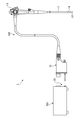
図1は、本実施形態の電子内視鏡システム1の外観図である。図1に示されるように、本実施形態の電子内視鏡システム1は、電子スコープ100及びプロセッサ200を備えている。プロセッサ200は、電子スコープ100からの信号を処理する信号処理装置と、自然光の届かない体腔内を電子スコープ100を介して照射する光源装置とを一体に備えた装置である。別の実施形態では、信号処理装置と光源装置とを別体で構成してもよい。
FIG. 1 is an external view of an electronic endoscope system 1 according to the present embodiment. As shown in FIG. 1, the electronic endoscope system 1 of the present embodiment includes an
図1に示されるように、電子スコープ100は、可撓性を有するシースによって外装された挿入部可撓管11を備えている。挿入部可撓管11の先端部分(屈曲部14)は、挿入部可撓管11の基端に連結された手元操作部13からの遠隔操作に応じて屈曲する。屈曲機構は、一般的な内視鏡に組み込まれている周知の機構であり、手元操作部13の湾曲操作ノブの回転操作に連動した操作ワイヤの牽引によって屈曲部14を屈曲させる。屈曲部14の先端には、硬質性を有する樹脂製筐体によって外装された先端部12の基端が連結している。先端部12の方向が湾曲操作ノブの回転操作による屈曲動作に応じて変わることにより、電子スコープ100による撮影領域が移動する。
As shown in FIG. 1, the
プロセッサ200には、電子スコープ100の基端に設けられたコネクタ部10に対応する連結構造を持つコネクタ部20が設けられている。コネクタ部20は、コネクタ部10と機械的に接続されることにより、電子スコープ100とプロセッサ200とを電気的にかつ光学的に接続する。
The
図2は、本実施形態の電子内視鏡システム1の構成を示すブロック図である。図2に示されるように、電子内視鏡システム1には、モニタ300がプロセッサ200に接続されている。
FIG. 2 is a block diagram showing a configuration of the electronic endoscope system 1 of the present embodiment. As shown in FIG. 2, a
図2に示されるように、プロセッサ200は、システムコントローラ202、タイミングコントローラ204を有している。システムコントローラ202は、メモリ222に記憶された各種プログラムを実行することにより、電子内視鏡システム1の全体を統括的に制御する。また、システムコントローラ202は、操作パネル218に入力されるユーザ(術者又は補助者)による指示に応じて電子内視鏡システム1の各種設定を変更する。なお、操作パネル218の構成には種々の形態がある。操作パネル218の具体的構成としては、例えば、プロセッサ200のフロント面に実装された機能毎のハードウェアキーやタッチパネル式GUI(Graphical User Interface)、ハードウェアキーとGUIとの組合せ等が考えられる。タイミングコントローラ204は、各部の動作のタイミングを調整するクロックパルスを電子内視鏡システム1内の各回路に出力する。
As illustrated in FIG. 2, the
ランプ208は、ランプ電源イグナイタ206による始動後、主に可視光領域から不可視である赤外光領域に広がるスペクトルを持つ光(又は少なくとも可視光領域を含む光)を射出する。ランプ208には、キセノンランプ、ハロゲンランプ、メタルハライドランプ等の高輝度ランプが適している。ランプ208より射出された照射光は、集光レンズ210によって集光されつつ絞り212を介して適正な光量に制限される。
After starting by the
絞り212には、図示省略されたアームやギヤ等の伝達機構を介してモータ214が機械的に連結している。モータ214は例えばDCモータであり、ドライバ216のドライブ制御下で駆動する。絞り212は、モニタ300の表示画面に表示される映像を適正な明るさにするため、モータ214により動作され開度が変えられる。ランプ208より照射された光の光量は、絞り212の開度に応じて制限される。適正とされる映像の明るさの基準は、術者による操作パネル218の輝度調節操作に応じて設定変更される。なお、ドライバ216を制御して輝度調整を行う調光回路は周知の回路であり、本明細書においては省略することとする。
A
絞り212を通過した照射光は、LCB(Light Carrying Bundle)102の入射端に入射される。入射端よりLCB102内に入射された照射光は、LCB102内を全反射を繰り返すことによって伝播する。LCB102内を伝播した照射光は、電子スコープ100の先端部12内に配置されたLCB102の射出端より射出され、配光レンズ104を介して被写体を照射する。
Irradiation light that has passed through the
被写体からの戻り光は、対物レンズ106を介して固体撮像素子108の受光面上の各画素で光学像を結ぶ。固体撮像素子108は、補色市松型画素配置を有するインターレース方式の単板式カラーCCD(Charge Coupled Device)イメージセンサである。固体撮像素子108は、受光面上の各画素で結像した光学像を光量に応じた電荷として蓄積して、イエローYe、シアンCy、グリーンG、マゼンタMgの各補色信号を生成し、生成された垂直方向に隣接する2つの画素の補色信号を加算し混合して順次出力する。以下、固体撮像素子108より順次出力される、各フィールドの各水平ラインの各画素に対応する混合後の信号を「撮像信号」と記す。なお、固体撮像素子108は、CCDイメージセンサに限らず、CMOS(Complementary Metal Oxide Semiconductor)イメージセンサやその他の種類の撮像装置を採用してもよい。固体撮像素子108はまた、原色系フィルタ(ベイヤ配列フィルタ)を搭載したものであってもよい。
Return light from the subject forms an optical image at each pixel on the light receiving surface of the solid-
固体撮像素子108より出力される撮像信号は、プリアンプ110による信号増幅後、ドライバ信号処理回路112を介して信号処理回路220に入力される。
The imaging signal output from the solid-
電子スコープ100には、ドライバ信号処理回路112及びメモリ114が備えられている。ドライバ信号処理回路112は、メモリ114にアクセスして電子スコープ100の固有情報を読み出す。メモリ114に記録される電子スコープ100の固有情報には、例えば、固体撮像素子108の画素数や感度、動作可能なフィールドレート(フレームレート)、型番等が含まれる。ドライバ信号処理回路112は、メモリ114より読み出された固有情報をシステムコントローラ202に出力する。
The
システムコントローラ202は、電子スコープ100の固有情報に基づいて各種演算を行い、制御信号を生成する。システムコントローラ202は、生成された制御信号を用いて、プロセッサ200に接続中の電子スコープに適した処理がされるようにプロセッサ200内の各種回路の動作やタイミングを制御する。
The
タイミングコントローラ204は、システムコントローラ202によるタイミング制御に従って、ドライバ信号処理回路112及び信号処理回路220にクロックパルスを供給する。ドライバ信号処理回路112は、タイミングコントローラ204から供給されるクロックパルスに従って、固体撮像素子108をプロセッサ200側で処理される映像のフィールドレート(フレームレート)に同期したタイミングで駆動制御する。
The timing controller 204 supplies clock pulses to the driver
図2に示されるように、信号処理回路220は、前段信号処理回路220A、ノイズリダクション回路220B及び後段信号処理回路220Cを備えている。
As shown in FIG. 2, the
前段信号処理回路220Aは、ドライバ信号処理回路112より入力される撮像信号に対して色補完、Y/C分離等の所定の信号処理を施して画素信号(輝度信号Y、色差信号U、V)を生成し、生成された画素信号をノイズリダクション回路220Bに出力する。
The pre-stage
図3は、ノイズリダクション回路220Bの構成を示すブロック図である。図3に示されるように、ノイズリダクション回路220Bは、第1フィールドメモリ220Ba、帰還係数算出部220Bb、乗算回路220Bc1〜220Bc3、第2フィールドメモリ220Bd、乗算回路220Be1〜220Be3及び加算回路220Bf1〜220Bf3を備えている。
FIG. 3 is a block diagram showing a configuration of the
第1フィールドメモリ220Baには、前段信号処理回路220Aより画素信号(輝度信号Y)が入力される。第1フィールドメモリ220Baには、少なくとも1フィールド分の画素信号(有効画素領域内の画素信号)がバッファリングされる。
A pixel signal (luminance signal Y) is input to the first field memory 220Ba from the previous stage
帰還係数算出部220Bbには、前段信号処理回路220Aより現在のフィールドの画素信号(輝度信号Y)が順次入力されると同時に、第1フィールドメモリ220Baより当該画素信号に対応する1フィールド前の画素信号(輝度信号Y)が順次入力される。ここでは、同一ライン且つ同一アドレスの画素の画素信号同士を「対応する画素信号」とする。例えば、奇数フィールドの水平2ライン目で最初に出力される画素信号に対応する、1フィールド前の画素信号は、1つ前の偶数フィールドの水平2ライン目で最初に出力された画素信号である。
The feedback coefficient calculation unit 220Bb sequentially receives the pixel signal (luminance signal Y) of the current field from the previous stage
[帰還係数算出部220Bbの動作の説明]
図4は、帰還係数算出部220Bbの動作を示すフローチャートである。
[Description of Operation of Feedback Coefficient Calculation Unit 220Bb]
FIG. 4 is a flowchart showing the operation of the feedback coefficient calculation unit 220Bb.
[図4のS11(輝度差分値の計算)]
図4に示されるように、本処理ステップS11では、有効画素領域内の各画素について、現在のフィールドの画素信号(輝度信号Y)と1つ前のフィールドの画素信号(輝度信号Y)との差分値が計算される。以下、説明の便宜上、本処理ステップS11にて計算される画素信号(輝度信号Y)の差分値を「輝度差分値」と記す。また、現在のフィールドの画素信号(輝度信号Y、色差信号U、V)を「現フィールド画素信号nfs」と記し、1つ前のフィールドの画素信号(輝度信号Y、色差信号U、V)を「前フィールド画素信号pfs」と記す。
[S11 in FIG. 4 (Calculation of Luminance Difference Value)]
As shown in FIG. 4, in this processing step S11, for each pixel in the effective pixel area, the pixel signal (luminance signal Y) of the current field and the pixel signal (luminance signal Y) of the previous field are calculated. The difference value is calculated. Hereinafter, for convenience of explanation, the difference value of the pixel signal (luminance signal Y) calculated in this processing step S11 is referred to as “luminance difference value”. Further, the pixel signal (luminance signal Y, color difference signals U, V) of the current field is denoted as “current field pixel signal nfs”, and the pixel signal (luminance signal Y, color difference signals U, V) of the previous field is indicated. This is referred to as “previous field pixel signal pfs”.
[図4のS12(第1カウント値の算出)]
図5(a)は、フィールド全体での動き検出を概念的に示す図である。本処理ステップS12では、図5(a)に示されるようにフィールド全体での動き検出を行うため、以下の処理が行われる。
[S12 in FIG. 4 (Calculation of First Count Value)]
FIG. 5A is a diagram conceptually illustrating motion detection in the entire field. In this processing step S12, the following processing is performed in order to detect motion in the entire field as shown in FIG.
本処理ステップS12では、有効画素領域内の画素の中で処理ステップS11にて計算された輝度差分値が第1の閾値よりも大きいものがカウントされる。すなわち、本処理ステップS12では、フィールド全体での動き検出を行うため、連続する2フィールドについて、フィールド全体を範囲として、輝度差分値が第1の閾値よりも大きい画素がカウントされる。以下、説明の便宜上、本処理ステップS12にてカウントされた画素の数を「第1カウント値」と記す。 In this processing step S12, the pixels in the effective pixel area whose luminance difference value calculated in the processing step S11 is larger than the first threshold are counted. That is, in this processing step S12, since motion detection is performed for the entire field, pixels having a luminance difference value larger than the first threshold are counted for the two consecutive fields over the entire field. Hereinafter, for convenience of explanation, the number of pixels counted in this processing step S12 is referred to as “first count value”.
[図4のS13(第1の値m1への変換)]
本処理ステップS13では、処理ステップS12にてカウントされた第1カウント値を第1の値m1に変換する。ここで、図6(a)に、第1カウント値と第1の値m1との変換関数をグラフ化して示す。図6(a)中、縦軸は、第1の値m1を示し、横軸は、第1カウント値を示す。第1の値m1は、「0〜9」の値をとる。
[S13 in FIG. 4 (Conversion to First Value m1)]
In the processing step S13, the first count value counted in the processing step S12 is converted into a first value m1. Here, FIG. 6A is a graph showing the conversion function between the first count value and the first value m1. In FIG. 6A, the vertical axis represents the first value m1, and the horizontal axis represents the first count value. The first value m1 takes a value of “0-9”.
図6(a)に示されるように、第1カウント値は、一定値C以下のときには一定値(ここでは「9」)に変換され、一定値Cより大きいほど小さい値に変換される。より詳細には、第1カウント値は、一定値Cより大きいほど「9」に対して小さい値に変換され、最大値となるとき(すなわち、有効画素領域内の全ての画素において輝度差分値が第1の閾値よりも大きいとき)には「0」に変換される。 As shown in FIG. 6A, the first count value is converted to a constant value (here, “9”) when it is less than or equal to a certain value C, and is converted to a smaller value as it is larger than the certain value C. More specifically, when the first count value is larger than the constant value C, the first count value is converted to a smaller value with respect to “9”, and when the first count value becomes the maximum value (that is, the luminance difference value is increased in all pixels in the effective pixel region). When it is larger than the first threshold value), it is converted to “0”.
第1の値m1は、傾向として、フィールド全体の中で被写体の動く領域が多い(輝度差分値が第1の閾値よりも大きい画素が多い)場合に小さい値をとり、フィールド全体の中で被写体の動く領域が少ない(輝度差分値が第1の閾値よりも大きい画素が少ない)場合に大きい値をとる。より簡潔には、フィールド全体を検出範囲とした場合に、第1の値m1は、被写体が動いていれば小さい値をとり、被写体が動いていなければ大きい値をとる。 The first value m1 tends to be a small value when there are many moving areas of the subject in the entire field (there are many pixels whose luminance difference value is larger than the first threshold value), and the subject is within the entire field. Takes a large value when there are few moving regions (the number of pixels having a luminance difference value larger than the first threshold value is small). More simply, when the entire field is the detection range, the first value m1 takes a small value if the subject is moving, and takes a large value if the subject is not moving.
[図4のS14(注目画素の設定)]
本処理ステップS14では、有効画素領域内の一つの画素が注目画素として設定される。
[S14 in FIG. 4 (Target Pixel Setting)]
In this processing step S14, one pixel in the effective pixel region is set as the target pixel.
[図4のS15(局所領域(画素群)の設定)]
本処理ステップS15では、処理ステップS14にて設定された注目画素及びその周辺画素よりなる画素群を設定する。なお、本実施形態において、周辺画素は、注目画素の上下左右方向、右斜め上方向、右斜め下方向、左斜め上方向及び左斜め下方向の各方向に隣接して位置する計8つの画素を指す。すなわち、画素群は、3×3のマトリクスに配置された9つの画素よりなる。
[S15 in FIG. 4 (Setting of Local Area (Pixel Group))]
In this processing step S15, a pixel group including the target pixel set in processing step S14 and its peripheral pixels is set. In the present embodiment, the peripheral pixels are a total of eight pixels located adjacent to each direction of the target pixel in the vertical and horizontal directions, diagonally upward to the right, diagonally downward to the right, diagonally upward to the left, and diagonally to the left. Point to. That is, the pixel group is composed of nine pixels arranged in a 3 × 3 matrix.
[図4のS16(第2カウント値の算出)]
図5(b)は、局所領域(画素群に対応する3×3の画素よりなる領域)での動き検出を概念的に示す図である。本処理ステップS16では、図5(b)に示されるように局所領域での動き検出を行うため、以下の処理が行われる。
[S16 in FIG. 4 (Calculation of Second Count Value)]
FIG. 5B is a diagram conceptually illustrating motion detection in a local region (region composed of 3 × 3 pixels corresponding to a pixel group). In this processing step S16, the following processing is performed in order to perform motion detection in the local region as shown in FIG.
本処理ステップS16では、画素群(1つの注目画素+8つの周辺画素)の中で処理ステップS11にて計算された輝度差分値が第2の閾値よりも小さいものがカウントされる。すなわち、本処理ステップS16では、局所領域での動き検出を行うため、連続する2フィールドについて、処理ステップS15にて設定された画素群を範囲として、輝度差分値が第2の閾値よりも小さい画素がカウントされる。以下、説明の便宜上、本処理ステップS16にてカウントされた画素の数を「第2カウント値」と記す。 In this processing step S16, the pixel group (one target pixel + 8 neighboring pixels) in which the luminance difference value calculated in the processing step S11 is smaller than the second threshold is counted. That is, in this processing step S16, in order to perform motion detection in the local region, pixels having a luminance difference value smaller than the second threshold value for the two consecutive fields with the pixel group set in the processing step S15 as a range. Is counted. Hereinafter, for convenience of explanation, the number of pixels counted in this processing step S16 is referred to as a “second count value”.
[図4のS17(第2の値m2への変換)]
本処理ステップS17では、処理ステップS16にてカウントされた第2カウント値を第2の値m2に変換する。ここで、図6(b)に、第2カウント値と第2の値m2との変換関数をグラフ化して示す。図6(b)中、縦軸は、第2の値m2を示し、横軸は、第2カウント値を示す。第2の値m2も第1の値m1と同じく「0〜9」の値をとる。
[S17 in FIG. 4 (Conversion to Second Value m2)]
In this processing step S17, the second count value counted in the processing step S16 is converted into a second value m2. Here, FIG. 6B is a graph showing the conversion function between the second count value and the second value m2. In FIG. 6B, the vertical axis represents the second value m2, and the horizontal axis represents the second count value. Similarly to the first value m1, the second value m2 takes a value of “0-9”.
図6(b)に示されるように、第2カウント値は、輝度差分値が第2の閾値よりも小さい画素の数そのもの(「0〜9」の値)に変換される。すなわち、第2の値m1は、第2カウント値そのままの値をとる。 As shown in FIG. 6B, the second count value is converted into the number of pixels (values “0 to 9”) whose luminance difference value is smaller than the second threshold value. That is, the second value m1 is the same value as the second count value.
第2の値m2は、局所領域内で被写体の動く領域が多い(輝度差分値が第2の閾値よりも大きい画素が多い)場合に小さい値をとり、局所領域内で被写体の動く領域が少ない(輝度差分値が第2の閾値よりも大きい画素が少ない)場合に大きい値をとる。より簡潔には、局所領域内を検出範囲とした場合に、第2の値m2は、被写体が動いていれば小さい値をとり、被写体が動いていなければ大きい値をとる。 The second value m2 takes a small value when there are many moving areas of the subject in the local area (there are many pixels whose luminance difference value is larger than the second threshold), and there are few moving areas of the subject within the local area. When the luminance difference value is smaller than the second threshold, there is a large value. More succinctly, when the local area is set as the detection range, the second value m2 takes a small value if the subject is moving, and takes a large value if the subject is not moving.
[図4のS18(第1の値m1と第2の値m2との比較)]
本処理ステップS18では、第1の値m1と第2の値m2との差分値が計算される。次いで、計算された差分値が第3の閾値以上であるか否かが判定される。
[S18 in FIG. 4 (Comparison between the first value m1 and the second value m2)]
In this processing step S18, a difference value between the first value m1 and the second value m2 is calculated. Next, it is determined whether or not the calculated difference value is greater than or equal to a third threshold value.
[図4のS19(帰還係数Kの算出)]
本処理ステップS19は、処理ステップS18にて計算された差分値が第3の閾値以上となる場合(S18:YES)に行われる。処理ステップS18にて計算される差分値は、典型的には、下記のケース1やケース2の場合に第3の閾値以上となる。
[S19 in FIG. 4 (Calculation of Feedback Coefficient K)]
This processing step S19 is performed when the difference value calculated in the processing step S18 is greater than or equal to the third threshold (S18: YES). The difference value calculated in the processing step S18 is typically greater than or equal to the third threshold in case 1 and
(ケース1)
ケース1は、フィールド全体の中で被写体の動く領域が多く且つ局所領域内で被写体の動く領域が少ないケースである。ケース1では、例えば、被写体の動いている部分がフィールド内で広く分布するが、局所的な領域を見ると被写体があまり動いていないため、フィールド全体では被写体が動いていると検出されるが、局所領域では被写体が動いていないと検出される。
(Case 1)
Case 1 is a case where there are many regions where the subject moves in the entire field and there are few regions where the subject moves within the local region. In Case 1, for example, the moving part of the subject is widely distributed in the field. However, since the subject does not move so much when looking at the local area, it is detected that the subject is moving in the entire field. It is detected that the subject is not moving in the local region.
(ケース2)
ケース2は、フィールド全体の中で被写体の動く領域が少なく且つ局所領域内で被写体の動く領域が多いケースである。ケース2では、例えば、フィールド全体を見ると被写体があまり動いていないが、局所的な領域を見ると被写体が動いているため、局所領域では被写体が動いていると検出されるが、フィールド全体では被写体が動いていないと検出される。
(Case 2)
このように、処理ステップS18にて計算された差分値が第3の閾値以上となる場合は、フィールド全体で見たときと局所領域で見たときとで被写体の動き検出の結果が異なる。そのため、局所領域(画素群)に属する注目画素の画素信号については、フィールド全体で被写体の動きを見たときと局所領域で被写体の動きを見たときの両方の状況を考慮することが望ましい。そこで、本処理ステップS19では、局所領域(画素群)に属する注目画素の画素信号に適用する帰還係数Kが次式により算出される。 As described above, when the difference value calculated in the processing step S18 is equal to or larger than the third threshold value, the result of the motion detection of the subject is different when viewed in the entire field and when viewed in the local region. For this reason, regarding the pixel signal of the target pixel belonging to the local region (pixel group), it is desirable to consider both the situation when the motion of the subject is observed in the entire field and the motion of the subject in the local region. Therefore, in this processing step S19, the feedback coefficient K applied to the pixel signal of the target pixel belonging to the local region (pixel group) is calculated by the following equation.
K=[(m1+m2)/2]/9 K = [(m1 + m2) / 2] / 9
[図4のS20(帰還係数Kの算出)]
本処理ステップS20は、処理ステップS18にて計算された差分値が第3の閾値未満となる場合(S18:NO)に行われる。処理ステップS18にて計算される差分値は、典型的には、下記のケース3やケース4の場合に第3の閾値未満となる。
[S20 in FIG. 4 (Calculation of Feedback Coefficient K)]
This processing step S20 is performed when the difference value calculated in the processing step S18 is less than the third threshold (S18: NO). The difference value calculated in the processing step S18 is typically less than the third threshold in the case 3 and case 4 below.
(ケース3)
ケース3は、フィールド全体の中で被写体の動く領域が少なく且つ局所領域内でも被写体の動く領域が少ないケースである。ケース3では、例えば、フィールド全体だけでなく局所的な領域を見ても被写体があまり動いていないため、何れの検出範囲でも被写体が動いていないと検出される。
(Case 3)
Case 3 is a case where there are few moving areas of the subject in the entire field and there are few moving areas of the subject even in the local area. In Case 3, for example, since the subject does not move so much not only in the entire field but also in a local region, it is detected that the subject does not move in any detection range.
(ケース4)
ケース4は、フィールド全体の中で被写体の動く領域が多く且つ局所領域内でも被写体の動く領域が多いケースである。ケース4では、例えば、動いている被写体がフィールド内で広く分布し、局所的な領域を見ても被写体が動いているため、何れも検出範囲でも被写体が動いていると検出される。
(Case 4)
Case 4 is a case where there are many regions where the subject moves in the entire field, and there are many regions where the subject moves even within the local region. In Case 4, for example, moving subjects are widely distributed in the field, and the subject is moving even if a local area is seen. Therefore, it is detected that the subject is moving in any detection range.
このように、処理ステップS18にて計算された差分値が第3の閾値未満となる場合は、フィールド全体で見たときと局所領域で見たときとで被写体の動き検出の結果が同じとなる。そのため、局所領域(画素群)に属する注目画素の画素信号については、フィールド全体で被写体の動きを見たときと局所領域で被写体の動きを見たときの一方の状況を考慮すればよい。そこで、本処理ステップS20では、局所領域(画素群)に属する注目画素の画素信号に適用する帰還係数Kが次式により算出される。 As described above, when the difference value calculated in the processing step S18 is less than the third threshold value, the result of subject motion detection is the same when viewed in the entire field and when viewed in the local region. . For this reason, regarding the pixel signal of the pixel of interest belonging to the local region (pixel group), it is only necessary to consider one of the situation when the subject motion is observed in the entire field and the subject motion is viewed in the local region. Therefore, in this processing step S20, the feedback coefficient K applied to the pixel signal of the target pixel belonging to the local region (pixel group) is calculated by the following equation.
K=m1/9 K = m1 / 9
なお、別の実施形態では、上記式を次式に置き換えてもよい。 In another embodiment, the above formula may be replaced with the following formula.
K=m2/9 K = m2 / 9
[図4のS21及びS22(未処理の画素の判定)]
本処理ステップS21では、有効画素領域内において、適用する帰還係数Kが算出されていない画素が残っているか否かが判定される。適用する帰還係数Kが算出されていない画素が残っている場合(S21:YES)、注目画素が次の画素(例えば水平ライン方向に隣接する画素)に設定される(S22)。次の注目画素が設定されると、本フローチャートは、処理ステップS15に戻る。処理ステップS15〜S22がループすることで、有効画素領域内の各画素について帰還係数Kが順次算出される。本フローチャートは、有効画素領域内の全ての画素について帰還係数Kが算出されると(S21:NO)、上記ループから抜けて終了する。
[S21 and S22 in FIG. 4 (determination of unprocessed pixels)]
In this processing step S21, it is determined whether or not there remains a pixel for which the applied feedback coefficient K has not been calculated in the effective pixel region. When a pixel for which the feedback coefficient K to be applied has not been calculated remains (S21: YES), the target pixel is set to the next pixel (for example, a pixel adjacent in the horizontal line direction) (S22). When the next pixel of interest is set, the flowchart returns to process step S15. As the processing steps S15 to S22 are looped, the feedback coefficient K is sequentially calculated for each pixel in the effective pixel region. When the feedback coefficient K is calculated for all the pixels in the effective pixel area (S21: NO), this flowchart exits from the loop and ends.
帰還係数算出部220Bbにて算出された帰還係数Kは、乗算回路220Bc1〜220Bc3及び乗算回路220Be1〜220Be3に入力される。 The feedback coefficient K calculated by the feedback coefficient calculation unit 220Bb is input to the multiplication circuits 220Bc1 to 220Bc3 and the multiplication circuits 220Be1 to 220Be3.
乗算回路220Bc1〜220Bc3にはそれぞれ、前段信号処理回路220Aより、現フィールド画素信号nfs(輝度信号Y)、現フィールド画素信号nfs(色差信号U)、現フィールド画素信号nfs(色差信号V)が入力される。乗算回路220Bc1〜220Bc3に入力された現フィールド画素信号nfs(輝度信号Y)、現フィールド画素信号nfs(色差信号U)、現フィールド画素信号nfs(色差信号V)はそれぞれ、(1−帰還係数K)の値で乗算される。以下、説明の便宜上、乗算回路220Bc1〜220Bc3による乗算値をそれぞれ、「乗算値(輝度信号Y)[nfs×(1−K)]」、「乗算値(色差信号U)[nfs×(1−K)]」、「乗算値(色差信号V)[nfs×(1−K)]」と記す。
Each of the multiplication circuits 220Bc1 to 220Bc3 receives the current field pixel signal nfs (luminance signal Y), the current field pixel signal nfs (color difference signal U), and the current field pixel signal nfs (color difference signal V) from the previous stage
乗算値(輝度信号Y)[nfs×(1−K)]、乗算値(色差信号U)[nfs×(1−K)]、乗算値(色差信号V)[nfs×(1−K)]はそれぞれ、加算回路220Bf1〜220Bf3に入力される。 Multiplication value (luminance signal Y) [nfs × (1-K)], multiplication value (color difference signal U) [nfs × (1-K)], multiplication value (color difference signal V) [nfs × (1-K)] Are respectively input to the addition circuits 220Bf1 to 220Bf3.
第2フィールドメモリ220Bdには、加算回路220Bf1〜220Bf3より出力される補正後の画像信号(輝度信号Y、色差信号U、V)が入力される。なお、補正後の画像信号とはノイズ低減後の画像信号であり、詳しくは後述する。第2フィールドメモリ220Bdには、少なくとも1フィールド分の画素信号(有効画素領域内の画素信号)がバッファリングされる。 The corrected image signals (luminance signal Y and color difference signals U and V) output from the addition circuits 220Bf1 to 220Bf3 are input to the second field memory 220Bd. The corrected image signal is an image signal after noise reduction, which will be described in detail later. In the second field memory 220Bd, pixel signals for at least one field (pixel signals in the effective pixel region) are buffered.
乗算回路220Be1〜220Be3にはそれぞれ、第2フィールドメモリ220Bdより、前フィールド画素信号pfs(補正後の輝度信号Y)、前フィールド画素信号pfs(補正後の色差信号U)、前フィールド画素信号pfs(補正後の色差信号V)が入力される。乗算回路220Be1〜220Be3に入力された前フィールド画素信号pfs(補正後の輝度信号Y)、前フィールド画素信号pfs(補正後の色差信号U)、前フィールド画素信号pfs(補正後の色差信号V)はそれぞれ、帰還係数Kで乗算される。以下、説明の便宜上、乗算回路220Be1〜220Be3による乗算値をそれぞれ、「乗算値(輝度信号Y)[pfs×K]」、「乗算値(色差信号U)[pfs×K]」、「乗算値(色差信号V)[pfs×K]」と記す。 The multiplication circuits 220Be1 to 220Be3 respectively receive the previous field pixel signal pfs (corrected luminance signal Y), the previous field pixel signal pfs (corrected color difference signal U), and the previous field pixel signal pfs (from the second field memory 220Bd. The corrected color difference signal V) is input. Previous field pixel signal pfs (corrected luminance signal Y), previous field pixel signal pfs (corrected color difference signal U), and previous field pixel signal pfs (corrected color difference signal V) input to the multiplication circuits 220Be1 to 220Be3. Are each multiplied by a feedback factor K. Hereinafter, for convenience of explanation, the multiplication values obtained by the multiplication circuits 220Be1 to 220Be3 are represented by “multiplication value (luminance signal Y) [pfs × K]”, “multiplication value (color difference signal U) [pfs × K]”, and “multiplication value”, respectively. (Color difference signal V) [pfs × K] ”.
乗算値(輝度信号Y)[pfs×K]、乗算値(色差信号U)[pfs×K]、乗算値(色差信号V)[pfs×K]はそれぞれ、加算回路220Bf1〜220Bf3に入力される。 The multiplication value (luminance signal Y) [pfs × K], the multiplication value (color difference signal U) [pfs × K], and the multiplication value (color difference signal V) [pfs × K] are input to the addition circuits 220Bf1 to 220Bf3, respectively. .
加算回路220Bf1は、乗算回路220Bc1より入力される乗算値(輝度信号Y)[nfs×(1−K)]と、乗算回路220Be1より入力される乗算値(輝度信号Y)[pfs×K]とを加算して、後段信号処理回路220Cに出力する。加算回路220Bf2は、乗算回路220Bc2より入力される乗算値(色差信号U)[nfs×(1−K)]と、乗算回路220Be2より入力される乗算値(色差信号U)[pfs×K]とを加算して、後段信号処理回路220Cに出力する。加算回路220Bf3は、乗算回路220Bc3より入力される乗算値(色差信号V)[nfs×(1−K)]と、乗算回路220Be3より入力される乗算値(色差信号V)[pfs×K]とを加算して、後段信号処理回路220Cに出力する。
The addition circuit 220Bf1 has a multiplication value (luminance signal Y) [nfs × (1-K)] input from the multiplication circuit 220Bc1 and a multiplication value (luminance signal Y) [pfs × K] input from the multiplication circuit 220Be1. Are output to the post-stage
すなわち、加算回路Bf1〜Bf3は、次式により、現フィールド画素信号nfsと前フィールド画素信号pfsとを混合することで、現フィールド画素信号nfsを補正する。次式に示されるように、現フィールド画素信号nfsと前フィールド画素信号pfsとの混合比は、帰還係数Kに応じて決まる。帰還係数Kは、被写体に動きがあるほど小さい値となり、被写体に動きがないほど大きい値となる。帰還係数Kが0に近いほど現フィールド画素信号nfsの比率が高くなるため、当該画素におけるノイズリダクション効果が小さくなる代わりに残像が抑えられる。また、帰還係数Kが1に近いほど前フィールド画素信号pfsの比率が高くなるため、当該画素におけるノイズリダクション効果が高くなる。 That is, the addition circuits Bf1 to Bf3 correct the current field pixel signal nfs by mixing the current field pixel signal nfs and the previous field pixel signal pfs according to the following equation. As shown in the following equation, the mixing ratio between the current field pixel signal nfs and the previous field pixel signal pfs is determined according to the feedback coefficient K. The feedback coefficient K decreases as the subject moves, and increases as the subject does not move. Since the ratio of the current field pixel signal nfs becomes higher as the feedback coefficient K is closer to 0, the afterimage is suppressed instead of reducing the noise reduction effect in the pixel. Further, since the ratio of the previous field pixel signal pfs becomes higher as the feedback coefficient K is closer to 1, the noise reduction effect in the pixel becomes higher.
補正後の現フィールド画素信号nfs’=[nfs×(1−K)]+[pfs×K] Corrected current field pixel signal nfs ′ = [nfs × (1−K)] + [pfs × K]
後段信号処理回路220Cは、加算回路220Bf1〜220Bf3より入力される補正後の現フィールド画素信号nfs’(輝度信号Y、色差信号U、V)をNTSC(National Television System Committee)やPAL(Phase Alternating Line)等の所定の規格に準拠したビデオ信号に変換し、変換されたビデオ信号をモニタ300に出力する。ビデオ信号がモニタ300に順次入力することにより、被写体のカラー画像がモニタ300の表示画面に表示される。
The post-stage
このように、本実施形態によれば、フィールド全体での被写体の動き検出の結果と局所領域での被写体の動き検出の結果の両方を考慮して各画素の帰還係数Kを算出することにより、動きのある被写体の残像を抑えつつ画像内のノイズを低減させられる。 As described above, according to the present embodiment, by calculating the feedback coefficient K of each pixel in consideration of both the result of subject motion detection in the entire field and the result of subject motion detection in the local region, Noise in an image can be reduced while suppressing an afterimage of a moving subject.
以上が本発明の例示的な実施形態の説明である。本発明の実施形態は、上記に説明したものに限定されず、本発明の技術的思想の範囲において様々な変形が可能である。例えば明細書中に例示的に明示される実施形態等又は自明な実施形態等を適宜組み合わせた内容も本願の実施形態に含まれる。 The above is the description of the exemplary embodiments of the present invention. Embodiments of the present invention are not limited to those described above, and various modifications are possible within the scope of the technical idea of the present invention. For example, the embodiment of the present application also includes an embodiment that is exemplarily specified in the specification or a combination of obvious embodiments and the like as appropriate.
上記の実施形態では、固体撮像素子108の撮像期間がフィールド期間であるが、別の実施形態では、フレーム期間であってもよい。
In the above embodiment, the imaging period of the solid-
1 電子内視鏡システム
100 電子スコープ
200 プロセッサ
1
Claims (5)
前記有効画素領域内において前記差分値が第1の条件を満たす画素をカウントし、カウントされた画素の数を第1カウント値とする第1のカウント手段と、
前記有効画素領域内の各画素を注目画素として順次設定する注目画素設定手段と、
順次設定される注目画素及びその周辺画素よりなる画素群の中で前記差分値が第2の条件を満たすものをカウントし、カウントされた画素の数を第2カウント値とする第2のカウント手段と、
各前記注目画素について、当該注目画素が属する画素群における第2カウント値と前記第1カウント値に基づいて現在の撮像期間の画素信号と1つ前の撮像期間の画素信号との混合比を決定する混合比決定手段と、
前記各注目画素について、前記混合比決定手段により決定された混合比に基づいて現在の撮像期間の画素信号を補正する画素信号補正手段と、
を備える、
画像処理装置。 For each pixel in the effective pixel area of the image sensor that periodically images the subject in a predetermined imaging period, the pixel signal of the current imaging period and the pixel signal of the previous imaging period output from the image sensor A difference value calculating means for calculating a difference value;
First counting means for counting pixels in which the difference value satisfies a first condition in the effective pixel region, and setting the number of counted pixels as a first count value;
Pixel-of-interest setting means for sequentially setting each pixel in the effective pixel region as a pixel of interest;
Second counting means that counts the difference value satisfying the second condition among the pixel group composed of the target pixel and its peripheral pixels that are sequentially set, and sets the number of counted pixels as the second count value When,
For each pixel of interest, the mixing ratio between the pixel signal of the current imaging period and the pixel signal of the previous imaging period is determined based on the second count value and the first count value in the pixel group to which the pixel of interest belongs. Means for determining the mixing ratio;
For each pixel of interest, pixel signal correction means for correcting the pixel signal of the current imaging period based on the mixture ratio determined by the mixture ratio determination means;
Comprising
Image processing device.
前記第1カウント値を第1の値に変換し、
前記第2カウント値を第2の値に変換し、
前記第1の値と前記第2の値との差分値に基づいて現在の撮像期間の画素信号と1つ前の撮像期間の画素信号との混合比を決定する、
請求項1に記載の画像処理装置。 The mixing ratio determining means includes
Converting the first count value to a first value;
Converting the second count value into a second value;
Determining a mixing ratio between the pixel signal of the current imaging period and the pixel signal of the previous imaging period based on a difference value between the first value and the second value;
The image processing apparatus according to claim 1 .
請求項2に記載の画像処理装置。 The numerical range of the first value and the numerical range of the second value are the same.
The image processing apparatus according to claim 2 .
前記差分値が第1の閾値よりも大きいことであり、
前記第2の条件は、
前記差分値が第2の閾値よりも小さいことであり、
前記第1カウント値は、
一定値以下のときには前記数値範囲内の最大値に変換され、
前記一定値より大きいほど前記最大値に対して小さい値に変換され、
前記第2カウント値は、
前記第2カウント値そのままの値に変換され、
前記混合比決定手段は、
前記第1の値と前記第2の値との差分値が第3の閾値以上のときには該第1の値及び該第2の値に基づいて前記混合比を決定し、
前記第1の値と前記第2の値との差分値が第3の閾値未満のときには該第1の値又は該第2の値に基づいて前記混合比を決定する、
請求項3に記載の画像処理装置。 The first condition is:
The difference value is greater than a first threshold;
The second condition is:
The difference value is less than a second threshold;
The first count value is
When it is below a certain value, it is converted to the maximum value within the numerical range,
The larger the certain value, the smaller the value converted to the maximum value,
The second count value is
The second count value is converted into a value as it is,
The mixing ratio determining means includes
When the difference value between the first value and the second value is greater than or equal to a third threshold, the mixing ratio is determined based on the first value and the second value;
When the difference value between the first value and the second value is less than a third threshold, the mixing ratio is determined based on the first value or the second value;
The image processing apparatus according to claim 3 .
1フィールド期間又は1フレーム期間である、
請求項1から請求項4の何れか一項に記載の画像処理装置。 The imaging period is
One field period or one frame period,
The image processing apparatus according to any one of claims 1 to 4 .
Priority Applications (8)
| Application Number | Priority Date | Filing Date | Title |
|---|---|---|---|
| JP2014081918A JP6411768B2 (en) | 2014-04-11 | 2014-04-11 | Image processing device |
| US15/037,808 US9842383B2 (en) | 2014-04-11 | 2015-03-26 | Image processing device |
| KR1020167015786A KR101809476B1 (en) | 2014-04-11 | 2015-03-26 | Image processing device |
| EP15776531.4A EP3131286B1 (en) | 2014-04-11 | 2015-03-26 | Image processing device |
| CA2931074A CA2931074C (en) | 2014-04-11 | 2015-03-26 | Electronic endoscope system |
| PCT/JP2015/059360 WO2015156142A1 (en) | 2014-04-11 | 2015-03-26 | Image processing device |
| CN201580003142.6A CN105830433B (en) | 2014-04-11 | 2015-03-26 | Image processing equipment |
| AU2015244984A AU2015244984B2 (en) | 2014-04-11 | 2015-03-26 | Electronic Endoscope System |
Applications Claiming Priority (1)
| Application Number | Priority Date | Filing Date | Title |
|---|---|---|---|
| JP2014081918A JP6411768B2 (en) | 2014-04-11 | 2014-04-11 | Image processing device |
Publications (2)
| Publication Number | Publication Date |
|---|---|
| JP2015204486A JP2015204486A (en) | 2015-11-16 |
| JP6411768B2 true JP6411768B2 (en) | 2018-10-24 |
Family
ID=54287719
Family Applications (1)
| Application Number | Title | Priority Date | Filing Date |
|---|---|---|---|
| JP2014081918A Active JP6411768B2 (en) | 2014-04-11 | 2014-04-11 | Image processing device |
Country Status (8)
| Country | Link |
|---|---|
| US (1) | US9842383B2 (en) |
| EP (1) | EP3131286B1 (en) |
| JP (1) | JP6411768B2 (en) |
| KR (1) | KR101809476B1 (en) |
| CN (1) | CN105830433B (en) |
| AU (1) | AU2015244984B2 (en) |
| CA (1) | CA2931074C (en) |
| WO (1) | WO2015156142A1 (en) |
Families Citing this family (2)
| Publication number | Priority date | Publication date | Assignee | Title |
|---|---|---|---|---|
| CN109151348B (en) * | 2018-09-28 | 2021-01-08 | 维沃移动通信有限公司 | Image processing method, electronic equipment and computer readable storage medium |
| JP7219804B2 (en) * | 2019-02-20 | 2023-02-08 | 株式会社エビデント | Information processing device, information processing system, information processing method and program |
Family Cites Families (22)
| Publication number | Priority date | Publication date | Assignee | Title |
|---|---|---|---|---|
| DE68909271T2 (en) * | 1988-02-23 | 1994-03-24 | Philips Nv | Method and arrangement for estimating the extent of movement in a picture element of a television picture. |
| JP2934036B2 (en) * | 1991-03-07 | 1999-08-16 | 松下電器産業株式会社 | Motion detection method and noise reduction device |
| JP3660731B2 (en) | 1995-11-13 | 2005-06-15 | ペンタックス株式会社 | Electronic endoscope |
| JP2000502549A (en) * | 1996-10-24 | 2000-02-29 | フィリップス エレクトロニクス ネムローゼ フェンノートシャップ | Noise filter processing |
| US6130707A (en) | 1997-04-14 | 2000-10-10 | Philips Electronics N.A. Corp. | Video motion detector with global insensitivity |
| JP2000209507A (en) | 1999-01-12 | 2000-07-28 | Toshiba Corp | Low noise processing circuit for solid-state image pickup device |
| US6847408B1 (en) | 2000-07-27 | 2005-01-25 | Richard W. Webb | Method and apparatus for reducing noise in an image sequence |
| US7724307B2 (en) * | 2004-07-28 | 2010-05-25 | Broadcom Corporation | Method and system for noise reduction in digital video |
| EP1830561A4 (en) * | 2004-12-21 | 2009-08-05 | Sony Corp | Image processing device, image processing method, and image processing program |
| JP5052319B2 (en) * | 2007-12-17 | 2012-10-17 | オリンパス株式会社 | Movie noise reduction processing apparatus, movie noise reduction processing program, movie noise reduction processing method |
| JP2009290827A (en) | 2008-06-02 | 2009-12-10 | Sony Corp | Image processing apparatus, and image processing method |
| CN101859440A (en) * | 2010-05-31 | 2010-10-13 | 浙江捷尚视觉科技有限公司 | Block-based motion region detection method |
| CN101894378B (en) * | 2010-06-13 | 2012-09-05 | 南京航空航天大学 | Moving target visual tracking method and system based on double ROI (Region of Interest) |
| JP5653098B2 (en) | 2010-07-09 | 2015-01-14 | Hoya株式会社 | Noise removal device |
| JP5645636B2 (en) * | 2010-12-16 | 2014-12-24 | 三菱電機株式会社 | Frame interpolation apparatus and method |
| JP2012129913A (en) | 2010-12-17 | 2012-07-05 | Sanyo Electric Co Ltd | Noise reduction device |
| JP2012142829A (en) * | 2011-01-05 | 2012-07-26 | Sony Corp | Image processing device and image processing method |
| TWI459325B (en) * | 2011-05-13 | 2014-11-01 | Altek Corp | Digital image processing device and processing method thereof |
| JP2012257193A (en) * | 2011-05-13 | 2012-12-27 | Sony Corp | Image processing apparatus, image pickup apparatus, image processing method, and program |
| JP2013074571A (en) | 2011-09-29 | 2013-04-22 | Sony Corp | Image processing apparatus, image processing method, program, and recording medium |
| US9930352B2 (en) * | 2012-12-14 | 2018-03-27 | Sony Corporation | Reducing noise in an intraframe appearance cycle |
| KR101652658B1 (en) * | 2014-02-07 | 2016-08-30 | 가부시키가이샤 모르포 | Image processing device, image processing method, image processing program, and recording medium |
-
2014
- 2014-04-11 JP JP2014081918A patent/JP6411768B2/en active Active
-
2015
- 2015-03-26 EP EP15776531.4A patent/EP3131286B1/en active Active
- 2015-03-26 CA CA2931074A patent/CA2931074C/en active Active
- 2015-03-26 WO PCT/JP2015/059360 patent/WO2015156142A1/en active Application Filing
- 2015-03-26 CN CN201580003142.6A patent/CN105830433B/en active Active
- 2015-03-26 KR KR1020167015786A patent/KR101809476B1/en active IP Right Grant
- 2015-03-26 US US15/037,808 patent/US9842383B2/en active Active
- 2015-03-26 AU AU2015244984A patent/AU2015244984B2/en active Active
Also Published As
| Publication number | Publication date |
|---|---|
| JP2015204486A (en) | 2015-11-16 |
| WO2015156142A1 (en) | 2015-10-15 |
| KR101809476B1 (en) | 2017-12-15 |
| EP3131286B1 (en) | 2020-12-23 |
| CA2931074C (en) | 2018-04-03 |
| AU2015244984A1 (en) | 2016-06-09 |
| CN105830433A (en) | 2016-08-03 |
| EP3131286A1 (en) | 2017-02-15 |
| AU2015244984B2 (en) | 2018-01-18 |
| US9842383B2 (en) | 2017-12-12 |
| EP3131286A4 (en) | 2017-11-01 |
| US20160292828A1 (en) | 2016-10-06 |
| CN105830433B (en) | 2017-12-05 |
| CA2931074A1 (en) | 2015-10-15 |
| KR20160085340A (en) | 2016-07-15 |
Similar Documents
| Publication | Publication Date | Title |
|---|---|---|
| WO2017069024A1 (en) | Endoscope system | |
| US20170257591A1 (en) | Signal processing apparatus, image capturing apparatus, control apparatus, signal processing method, and control method | |
| US10548465B2 (en) | Medical imaging apparatus and medical observation system | |
| JP5708036B2 (en) | Imaging device | |
| JP6411768B2 (en) | Image processing device | |
| JP2019140528A (en) | Imaging apparatus and electronic apparatus | |
| JP2015195550A (en) | Imaging element and imaging device | |
| US20190380567A1 (en) | Electronic endoscope device | |
| JP6099009B2 (en) | Imaging device and imaging apparatus | |
| WO2018008009A1 (en) | Image processing device and electronic endoscope system | |
| JP2011176671A (en) | Imaging system | |
| JP2011156214A (en) | Imaging device and electronic endoscope system | |
| JP6272115B2 (en) | Endoscope processor and endoscope system | |
| JP6650969B2 (en) | Endoscope system | |
| JP2015047440A (en) | Processor | |
| JP6370604B2 (en) | Endoscope system | |
| JP6681971B2 (en) | Processor and endoscope system | |
| US20210251467A1 (en) | Image signal processing device, image signal processing method, and program | |
| JP2010279507A (en) | Electronic endoscopic system | |
| JP4764295B2 (en) | Infrared measurement display device | |
| JP6741412B2 (en) | Signal transmission device and electronic endoscope system | |
| JP2011172783A (en) | Image processor and electronic endoscope system | |
| JP6411816B2 (en) | Noise reduction device | |
| JP2012075807A (en) | Electronic endoscope apparatus | |
| JP2018161411A (en) | Electronic endoscope system and processing apparatus |
Legal Events
| Date | Code | Title | Description |
|---|---|---|---|
| A621 | Written request for application examination |
Free format text: JAPANESE INTERMEDIATE CODE: A621 Effective date: 20170123 |
|
| RD04 | Notification of resignation of power of attorney |
Free format text: JAPANESE INTERMEDIATE CODE: A7424 Effective date: 20170717 |
|
| A131 | Notification of reasons for refusal |
Free format text: JAPANESE INTERMEDIATE CODE: A131 Effective date: 20180313 |
|
| A521 | Request for written amendment filed |
Free format text: JAPANESE INTERMEDIATE CODE: A523 Effective date: 20180511 |
|
| TRDD | Decision of grant or rejection written | ||
| A01 | Written decision to grant a patent or to grant a registration (utility model) |
Free format text: JAPANESE INTERMEDIATE CODE: A01 Effective date: 20180903 |
|
| A61 | First payment of annual fees (during grant procedure) |
Free format text: JAPANESE INTERMEDIATE CODE: A61 Effective date: 20180927 |
|
| R150 | Certificate of patent or registration of utility model |
Ref document number: 6411768 Country of ref document: JP Free format text: JAPANESE INTERMEDIATE CODE: R150 |
|
| R250 | Receipt of annual fees |
Free format text: JAPANESE INTERMEDIATE CODE: R250 |
|
| R250 | Receipt of annual fees |
Free format text: JAPANESE INTERMEDIATE CODE: R250 |
|
| R250 | Receipt of annual fees |
Free format text: JAPANESE INTERMEDIATE CODE: R250 |