JP6368214B2 - Elastic wave device - Google Patents
Elastic wave device Download PDFInfo
- Publication number
- JP6368214B2 JP6368214B2 JP2014205260A JP2014205260A JP6368214B2 JP 6368214 B2 JP6368214 B2 JP 6368214B2 JP 2014205260 A JP2014205260 A JP 2014205260A JP 2014205260 A JP2014205260 A JP 2014205260A JP 6368214 B2 JP6368214 B2 JP 6368214B2
- Authority
- JP
- Japan
- Prior art keywords
- film
- silicon oxide
- oxide film
- piezoelectric
- insulating
- Prior art date
- Legal status (The legal status is an assumption and is not a legal conclusion. Google has not performed a legal analysis and makes no representation as to the accuracy of the status listed.)
- Active
Links
- VYPSYNLAJGMNEJ-UHFFFAOYSA-N Silicium dioxide Chemical compound O=[Si]=O VYPSYNLAJGMNEJ-UHFFFAOYSA-N 0.000 claims description 208
- 229910052814 silicon oxide Inorganic materials 0.000 claims description 201
- QVGXLLKOCUKJST-UHFFFAOYSA-N atomic oxygen Chemical compound [O] QVGXLLKOCUKJST-UHFFFAOYSA-N 0.000 claims description 73
- 229910052760 oxygen Inorganic materials 0.000 claims description 73
- 239000001301 oxygen Substances 0.000 claims description 73
- 239000000758 substrate Substances 0.000 claims description 44
- 229910052751 metal Inorganic materials 0.000 claims description 30
- 239000002184 metal Substances 0.000 claims description 30
- 239000000463 material Substances 0.000 claims description 22
- 239000011810 insulating material Substances 0.000 claims description 10
- PMHQVHHXPFUNSP-UHFFFAOYSA-M copper(1+);methylsulfanylmethane;bromide Chemical compound Br[Cu].CSC PMHQVHHXPFUNSP-UHFFFAOYSA-M 0.000 claims description 7
- PXGOKWXKJXAPGV-UHFFFAOYSA-N Fluorine Chemical compound FF PXGOKWXKJXAPGV-UHFFFAOYSA-N 0.000 claims description 5
- 229910052731 fluorine Inorganic materials 0.000 claims description 5
- 239000011737 fluorine Substances 0.000 claims description 5
- XUIMIQQOPSSXEZ-UHFFFAOYSA-N Silicon Chemical compound [Si] XUIMIQQOPSSXEZ-UHFFFAOYSA-N 0.000 claims description 4
- 239000012535 impurity Substances 0.000 claims description 4
- 229910052710 silicon Inorganic materials 0.000 claims description 4
- 239000010703 silicon Substances 0.000 claims description 4
- 150000004767 nitrides Chemical class 0.000 claims description 3
- 239000010408 film Substances 0.000 description 592
- 239000010409 thin film Substances 0.000 description 95
- 230000004048 modification Effects 0.000 description 56
- 238000012986 modification Methods 0.000 description 56
- 229910052581 Si3N4 Inorganic materials 0.000 description 26
- HQVNEWCFYHHQES-UHFFFAOYSA-N silicon nitride Chemical compound N12[Si]34N5[Si]62N3[Si]51N64 HQVNEWCFYHHQES-UHFFFAOYSA-N 0.000 description 26
- 230000000052 comparative effect Effects 0.000 description 19
- 230000006866 deterioration Effects 0.000 description 19
- 239000011651 chromium Substances 0.000 description 16
- 229910020177 SiOF Inorganic materials 0.000 description 11
- 230000003647 oxidation Effects 0.000 description 9
- 238000007254 oxidation reaction Methods 0.000 description 9
- 238000010521 absorption reaction Methods 0.000 description 8
- 230000000694 effects Effects 0.000 description 6
- 239000010931 gold Substances 0.000 description 5
- 239000010936 titanium Substances 0.000 description 5
- 239000010949 copper Substances 0.000 description 4
- 229910052707 ruthenium Inorganic materials 0.000 description 4
- 235000012239 silicon dioxide Nutrition 0.000 description 4
- PIGFYZPCRLYGLF-UHFFFAOYSA-N Aluminum nitride Chemical compound [Al]#N PIGFYZPCRLYGLF-UHFFFAOYSA-N 0.000 description 3
- 229910052782 aluminium Inorganic materials 0.000 description 3
- 229910052804 chromium Inorganic materials 0.000 description 3
- 229910052802 copper Inorganic materials 0.000 description 3
- BASFCYQUMIYNBI-UHFFFAOYSA-N platinum Chemical compound [Pt] BASFCYQUMIYNBI-UHFFFAOYSA-N 0.000 description 3
- 239000010948 rhodium Substances 0.000 description 3
- 239000000377 silicon dioxide Substances 0.000 description 3
- 238000010897 surface acoustic wave method Methods 0.000 description 3
- 229910052719 titanium Inorganic materials 0.000 description 3
- IJGRMHOSHXDMSA-UHFFFAOYSA-N Atomic nitrogen Chemical compound N#N IJGRMHOSHXDMSA-UHFFFAOYSA-N 0.000 description 2
- VYZAMTAEIAYCRO-UHFFFAOYSA-N Chromium Chemical compound [Cr] VYZAMTAEIAYCRO-UHFFFAOYSA-N 0.000 description 2
- KJTLSVCANCCWHF-UHFFFAOYSA-N Ruthenium Chemical compound [Ru] KJTLSVCANCCWHF-UHFFFAOYSA-N 0.000 description 2
- RTAQQCXQSZGOHL-UHFFFAOYSA-N Titanium Chemical compound [Ti] RTAQQCXQSZGOHL-UHFFFAOYSA-N 0.000 description 2
- 239000000460 chlorine Substances 0.000 description 2
- 238000010586 diagram Methods 0.000 description 2
- PCHJSUWPFVWCPO-UHFFFAOYSA-N gold Chemical compound [Au] PCHJSUWPFVWCPO-UHFFFAOYSA-N 0.000 description 2
- 229910052737 gold Inorganic materials 0.000 description 2
- 229910052451 lead zirconate titanate Inorganic materials 0.000 description 2
- 239000011777 magnesium Substances 0.000 description 2
- 150000002739 metals Chemical class 0.000 description 2
- 229910052750 molybdenum Inorganic materials 0.000 description 2
- 229910052703 rhodium Inorganic materials 0.000 description 2
- 229910052721 tungsten Inorganic materials 0.000 description 2
- XLYOFNOQVPJJNP-UHFFFAOYSA-N water Substances O XLYOFNOQVPJJNP-UHFFFAOYSA-N 0.000 description 2
- 229910018072 Al 2 O 3 Inorganic materials 0.000 description 1
- JBRZTFJDHDCESZ-UHFFFAOYSA-N AsGa Chemical compound [As]#[Ga] JBRZTFJDHDCESZ-UHFFFAOYSA-N 0.000 description 1
- ZOXJGFHDIHLPTG-UHFFFAOYSA-N Boron Chemical compound [B] ZOXJGFHDIHLPTG-UHFFFAOYSA-N 0.000 description 1
- OKTJSMMVPCPJKN-UHFFFAOYSA-N Carbon Chemical compound [C] OKTJSMMVPCPJKN-UHFFFAOYSA-N 0.000 description 1
- ZAMOUSCENKQFHK-UHFFFAOYSA-N Chlorine atom Chemical compound [Cl] ZAMOUSCENKQFHK-UHFFFAOYSA-N 0.000 description 1
- RYGMFSIKBFXOCR-UHFFFAOYSA-N Copper Chemical compound [Cu] RYGMFSIKBFXOCR-UHFFFAOYSA-N 0.000 description 1
- UFHFLCQGNIYNRP-UHFFFAOYSA-N Hydrogen Chemical compound [H][H] UFHFLCQGNIYNRP-UHFFFAOYSA-N 0.000 description 1
- FYYHWMGAXLPEAU-UHFFFAOYSA-N Magnesium Chemical compound [Mg] FYYHWMGAXLPEAU-UHFFFAOYSA-N 0.000 description 1
- ZOKXTWBITQBERF-UHFFFAOYSA-N Molybdenum Chemical compound [Mo] ZOKXTWBITQBERF-UHFFFAOYSA-N 0.000 description 1
- OAICVXFJPJFONN-UHFFFAOYSA-N Phosphorus Chemical compound [P] OAICVXFJPJFONN-UHFFFAOYSA-N 0.000 description 1
- 229910004298 SiO 2 Inorganic materials 0.000 description 1
- NINIDFKCEFEMDL-UHFFFAOYSA-N Sulfur Chemical compound [S] NINIDFKCEFEMDL-UHFFFAOYSA-N 0.000 description 1
- XLOMVQKBTHCTTD-UHFFFAOYSA-N Zinc monoxide Chemical compound [Zn]=O XLOMVQKBTHCTTD-UHFFFAOYSA-N 0.000 description 1
- XAGFODPZIPBFFR-UHFFFAOYSA-N aluminium Chemical compound [Al] XAGFODPZIPBFFR-UHFFFAOYSA-N 0.000 description 1
- 229910052796 boron Inorganic materials 0.000 description 1
- 229910052799 carbon Inorganic materials 0.000 description 1
- 230000015556 catabolic process Effects 0.000 description 1
- 239000000919 ceramic Substances 0.000 description 1
- 229910052801 chlorine Inorganic materials 0.000 description 1
- 230000008878 coupling Effects 0.000 description 1
- 238000010168 coupling process Methods 0.000 description 1
- 238000005859 coupling reaction Methods 0.000 description 1
- 238000006731 degradation reaction Methods 0.000 description 1
- NKZSPGSOXYXWQA-UHFFFAOYSA-N dioxido(oxo)titanium;lead(2+) Chemical compound [Pb+2].[O-][Ti]([O-])=O NKZSPGSOXYXWQA-UHFFFAOYSA-N 0.000 description 1
- 230000005284 excitation Effects 0.000 description 1
- 230000001747 exhibiting effect Effects 0.000 description 1
- 239000011521 glass Substances 0.000 description 1
- 229910052735 hafnium Inorganic materials 0.000 description 1
- VBJZVLUMGGDVMO-UHFFFAOYSA-N hafnium atom Chemical compound [Hf] VBJZVLUMGGDVMO-UHFFFAOYSA-N 0.000 description 1
- 229910052739 hydrogen Inorganic materials 0.000 description 1
- 239000001257 hydrogen Substances 0.000 description 1
- 229910052741 iridium Inorganic materials 0.000 description 1
- GKOZUEZYRPOHIO-UHFFFAOYSA-N iridium atom Chemical compound [Ir] GKOZUEZYRPOHIO-UHFFFAOYSA-N 0.000 description 1
- 238000010030 laminating Methods 0.000 description 1
- 239000010410 layer Substances 0.000 description 1
- HFGPZNIAWCZYJU-UHFFFAOYSA-N lead zirconate titanate Chemical compound [O-2].[O-2].[O-2].[O-2].[O-2].[Ti+4].[Zr+4].[Pb+2] HFGPZNIAWCZYJU-UHFFFAOYSA-N 0.000 description 1
- 229910052749 magnesium Inorganic materials 0.000 description 1
- 239000012528 membrane Substances 0.000 description 1
- 239000011733 molybdenum Substances 0.000 description 1
- 229910052757 nitrogen Inorganic materials 0.000 description 1
- TWNQGVIAIRXVLR-UHFFFAOYSA-N oxo(oxoalumanyloxy)alumane Chemical compound O=[Al]O[Al]=O TWNQGVIAIRXVLR-UHFFFAOYSA-N 0.000 description 1
- QVGXLLKOCUKJST-NJFSPNSNSA-N oxygen-18 atom Chemical compound [18O] QVGXLLKOCUKJST-NJFSPNSNSA-N 0.000 description 1
- 229910052698 phosphorus Inorganic materials 0.000 description 1
- 239000011574 phosphorus Substances 0.000 description 1
- 229910052697 platinum Inorganic materials 0.000 description 1
- 230000001902 propagating effect Effects 0.000 description 1
- 239000010453 quartz Substances 0.000 description 1
- MHOVAHRLVXNVSD-UHFFFAOYSA-N rhodium atom Chemical compound [Rh] MHOVAHRLVXNVSD-UHFFFAOYSA-N 0.000 description 1
- 229910052706 scandium Inorganic materials 0.000 description 1
- SIXSYDAISGFNSX-UHFFFAOYSA-N scandium atom Chemical compound [Sc] SIXSYDAISGFNSX-UHFFFAOYSA-N 0.000 description 1
- VSZWPYCFIRKVQL-UHFFFAOYSA-N selanylidenegallium;selenium Chemical compound [Se].[Se]=[Ga].[Se]=[Ga] VSZWPYCFIRKVQL-UHFFFAOYSA-N 0.000 description 1
- 239000002356 single layer Substances 0.000 description 1
- 229910052717 sulfur Inorganic materials 0.000 description 1
- 239000011593 sulfur Substances 0.000 description 1
- 229910052715 tantalum Inorganic materials 0.000 description 1
- GUVRBAGPIYLISA-UHFFFAOYSA-N tantalum atom Chemical compound [Ta] GUVRBAGPIYLISA-UHFFFAOYSA-N 0.000 description 1
- WFKWXMTUELFFGS-UHFFFAOYSA-N tungsten Chemical compound [W] WFKWXMTUELFFGS-UHFFFAOYSA-N 0.000 description 1
- 239000010937 tungsten Substances 0.000 description 1
- 239000011800 void material Substances 0.000 description 1
Images


Classifications
-
- H—ELECTRICITY
- H03—ELECTRONIC CIRCUITRY
- H03H—IMPEDANCE NETWORKS, e.g. RESONANT CIRCUITS; RESONATORS
- H03H9/00—Networks comprising electromechanical or electro-acoustic devices; Electromechanical resonators
- H03H9/15—Constructional features of resonators consisting of piezoelectric or electrostrictive material
- H03H9/17—Constructional features of resonators consisting of piezoelectric or electrostrictive material having a single resonator
- H03H9/171—Constructional features of resonators consisting of piezoelectric or electrostrictive material having a single resonator implemented with thin-film techniques, i.e. of the film bulk acoustic resonator [FBAR] type
-
- H—ELECTRICITY
- H03—ELECTRONIC CIRCUITRY
- H03H—IMPEDANCE NETWORKS, e.g. RESONANT CIRCUITS; RESONATORS
- H03H9/00—Networks comprising electromechanical or electro-acoustic devices; Electromechanical resonators
- H03H9/02—Details
- H03H9/02007—Details of bulk acoustic wave devices
- H03H9/02086—Means for compensation or elimination of undesirable effects
- H03H9/02102—Means for compensation or elimination of undesirable effects of temperature influence
Landscapes
- Physics & Mathematics (AREA)
- Acoustics & Sound (AREA)
- Piezo-Electric Or Mechanical Vibrators, Or Delay Or Filter Circuits (AREA)
Description
本発明は、弾性波デバイスに関する。 The present invention relates to an acoustic wave device.
携帯電話端末等の無線通信機器のフィルタ及びデュプレクサに、弾性波デバイスの一種である、バルク波(BAW:Bulk Acoustic Wave)を利用した圧電薄膜共振器が用いられている。圧電薄膜共振器は、下部電極と上部電極とが圧電膜を挟んで対向した構造をしている。圧電膜は、一般的に、弾性定数の温度係数が負であるため、共振周波数や反共振周波数が温度により変化する。そこで、周波数の温度変化を抑制するために、圧電膜とは逆符号の温度係数の弾性定数を有する酸化シリコン膜を温度補償膜として用いることが提案されている。例えば、ホウ素をドープした酸化シリコン膜を温度補償膜として用いることが提案されている(例えば、特許文献1参照)。例えば、LTO(Low Temperature Oxide)膜と窒化シリコン膜との積層膜を温度補償膜として用いることが提案されている(例えば、非特許文献1参照)。 Piezoelectric thin film resonators using a bulk acoustic wave (BAW), which is a kind of elastic wave device, are used in filters and duplexers of wireless communication devices such as mobile phone terminals. The piezoelectric thin film resonator has a structure in which a lower electrode and an upper electrode face each other with a piezoelectric film interposed therebetween. A piezoelectric film generally has a negative elastic coefficient of temperature coefficient, and therefore the resonance frequency and antiresonance frequency change with temperature. Therefore, in order to suppress the temperature change of the frequency, it has been proposed to use, as the temperature compensation film, a silicon oxide film having an elastic constant having a temperature coefficient opposite to that of the piezoelectric film. For example, it has been proposed to use a silicon oxide film doped with boron as a temperature compensation film (see, for example, Patent Document 1). For example, it has been proposed to use a laminated film of an LTO (Low Temperature Oxide) film and a silicon nitride film as a temperature compensation film (see, for example, Non-Patent Document 1).
また、弾性波デバイスの一種である弾性表面波(SAW:Surface Acoustic Wave)デバイスにおいて、櫛型電極を覆う二酸化シリコン膜の吸湿を抑制するために、二酸化シリコン膜上に窒化シリコン膜を設けることが知られている(例えば、特許文献2参照)。また、SAWデバイスにおいて、櫛型電極の吸湿を抑制するために、櫛型電極を覆って窒化シリコン膜を設けることが知られている(例えば、特許文献3参照)。 In addition, in a surface acoustic wave (SAW) device which is a kind of acoustic wave device, a silicon nitride film may be provided on the silicon dioxide film in order to suppress moisture absorption of the silicon dioxide film covering the comb-shaped electrode. It is known (see, for example, Patent Document 2). In a SAW device, it is known that a silicon nitride film is provided so as to cover the comb electrode in order to suppress moisture absorption of the comb electrode (see, for example, Patent Document 3).
圧電薄膜共振器において、温度補償膜として用いられる酸化シリコン膜は、下部電極及び上部電極の少なくとも一方の圧電膜に対して反対側に設けられる場合がある。この場合に、酸化シリコン膜が下部電極及び上部電極と接していると、例えば高温信頼性試験において、下部電極及び上部電極が酸化シリコン膜中の酸素によって酸化されることが生じる。また、酸化シリコン膜は吸湿性を示すため、例えば高温信頼性試験において、水分を吸収して膜質が変化することも生じる。これらは、共振器の特性劣化を引き起こす要因となる。 In a piezoelectric thin film resonator, a silicon oxide film used as a temperature compensation film may be provided on the opposite side of at least one of the lower electrode and the upper electrode. In this case, if the silicon oxide film is in contact with the lower electrode and the upper electrode, the lower electrode and the upper electrode may be oxidized by oxygen in the silicon oxide film, for example, in a high temperature reliability test. In addition, since the silicon oxide film exhibits hygroscopicity, for example, in a high temperature reliability test, the film quality may be changed by absorbing moisture. These are factors that cause deterioration of the characteristics of the resonator.
本発明は、上記課題に鑑みなされたものであり、特性の劣化を抑制することが可能な弾性波デバイスを提供することを目的とする。 The present invention has been made in view of the above problems, and an object of the present invention is to provide an elastic wave device capable of suppressing deterioration of characteristics.
本発明は、基板と、前記基板上に設けられた圧電膜と、前記圧電膜の少なくとも一部を挟んで対向した下部電極及び上部電極と、前記下部電極の前記圧電膜に対して反対側に設けられた酸化シリコン膜と、前記下部電極と前記酸化シリコン膜との間に設けられた酸素元素を含まない絶縁材料を有する第1絶縁膜と、前記酸化シリコン膜の前記第1絶縁膜に対して反対側に設けられ、前記酸化シリコン膜及び前記第1絶縁膜とは異なる材料である付加膜と、を備え、前記圧電膜は、前記酸化シリコン膜上から前記酸化シリコン膜の側方に延在していて、前記第1絶縁膜は、前記酸化シリコン膜の側面のうちの前記圧電膜で覆われた側面と前記圧電膜との間に延在している、弾性波デバイスである。 The present invention includes a substrate and a piezoelectric film provided on the substrate, a lower electrode and an upper electrode facing each other across at least a portion of the piezoelectric film, the opposite side with respect to the piezoelectric layer of the lower electrodes a silicon oxide film provided on a first insulating film having an insulating material which does not contain the oxygen element which is provided between the silicon oxide film and the lower electrodes, wherein the first insulating film of the silicon oxide film And an additional film made of a material different from that of the silicon oxide film and the first insulating film, and the piezoelectric film is formed on the side of the silicon oxide film from the silicon oxide film. The first insulating film is an acoustic wave device that extends between a side surface of the silicon oxide film covered with the piezoelectric film and the piezoelectric film. .
本発明は、基板と、前記基板上に設けられた圧電膜と、前記圧電膜の少なくとも一部を挟んで対向した下部電極及び上部電極と、前記下部電極及び前記上部電極の少なくとも一方の前記圧電膜に対して反対側に設けられたフッ素がドープされた酸化シリコン膜と、前記下部電極及び前記上部電極の少なくとも一方と前記酸化シリコン膜との間に設けられた酸素元素を含まない絶縁材料を有する第1絶縁膜と、前記酸化シリコン膜の前記第1絶縁膜に対して反対側に設けられ、前記酸化シリコン膜及び前記第1絶縁膜とは異なる材料である付加膜と、前記酸化シリコン膜の側面のうちの前記圧電膜又は前記付加膜で覆われていない側面に設けられ、前記酸化シリコン膜とは異なる材料からなる第2絶縁膜と、を備える、弾性波デバイスである。 The present invention includes a substrate, a piezoelectric film provided on the substrate, a lower electrode and an upper electrode facing each other with at least a part of the piezoelectric film interposed therebetween, and the piezoelectric of at least one of the lower electrode and the upper electrode. A fluorine-doped silicon oxide film provided on the opposite side of the film, and an insulating material containing no oxygen element provided between at least one of the lower electrode and the upper electrode and the silicon oxide film A first insulating film, an additional film that is provided on the opposite side of the silicon oxide film with respect to the first insulating film, and is made of a material different from the silicon oxide film and the first insulating film, and the silicon oxide film provided in the piezoelectric film or the not covered by the additional film side of the side surface, and a second insulating film made of a material different from that of the silicon oxide film is an elastic wave device.
本発明は、基板と、前記基板上に設けられた圧電膜と、前記圧電膜の少なくとも一部を挟んで対向した下部電極及び上部電極と、前記下部電極の前記圧電膜に対して反対側に設けられた酸化シリコン膜と、前記下部電極と前記酸化シリコン膜との間に設けられた酸素元素を含まない絶縁材料を有する第1絶縁膜と、前記酸化シリコン膜の前記第1絶縁膜に対して反対側に設けられ、前記酸化シリコン膜及び前記第1絶縁膜とは異なる材料である付加膜と、前記下部電極の上面に接して設けられた電極パッドと、を備え、前記電極パッド下には、前記酸化シリコン膜が設けられていない、弾性波デバイスである。 The present invention includes a substrate, a piezoelectric film provided on the substrate, a lower electrode and an upper electrode facing each other with at least a part of the piezoelectric film interposed therebetween, and an opposite side of the piezoelectric film to the lower electrode. A silicon oxide film provided; a first insulating film that is provided between the lower electrode and the silicon oxide film and includes an insulating material that does not include an oxygen element; and the first insulating film of the silicon oxide film An additional film made of a material different from that of the silicon oxide film and the first insulating film, and an electrode pad provided in contact with the upper surface of the lower electrode, and under the electrode pad Is an acoustic wave device not provided with the silicon oxide film .
本発明は、基板と、前記基板上に設けられた圧電膜と、前記圧電膜の少なくとも一部を挟んで対向した下部電極及び上部電極と、前記下部電極及び前記上部電極の少なくとも一方の前記圧電膜に対して反対側に設けられた酸化シリコン膜と、前記下部電極及び前記上部電極の少なくとも一方と前記酸化シリコン膜との間に設けられた酸素元素を含まない絶縁材料を有する第1絶縁膜と、前記酸化シリコン膜の前記第1絶縁膜に対して反対側に設けられ、前記酸化シリコン膜及び前記第1絶縁膜とは異なる材料である金属膜からなる付加膜と、を備える、弾性波デバイスである。 The present invention includes a substrate, a piezoelectric film provided on the substrate, a lower electrode and an upper electrode facing each other with at least a part of the piezoelectric film interposed therebetween, and the piezoelectric of at least one of the lower electrode and the upper electrode. A silicon oxide film provided on the opposite side of the film; and a first insulating film having an insulating material not including an oxygen element provided between at least one of the lower electrode and the upper electrode and the silicon oxide film And an additional film made of a metal film which is provided on the opposite side of the silicon oxide film with respect to the first insulating film and is made of a material different from the silicon oxide film and the first insulating film. It is a device .
本発明は、基板と、前記基板上に設けられた圧電膜と、前記圧電膜の少なくとも一部を挟んで対向した下部電極及び上部電極と、前記下部電極及び前記上部電極の少なくとも一方の前記圧電膜に対して反対側に設けられた酸化シリコン膜と、前記下部電極及び前記上部電極の少なくとも一方と前記酸化シリコン膜との間に設けられた酸素元素を含まない絶縁材料を有する第1絶縁膜と、前記酸化シリコン膜の前記第1絶縁膜に対して反対側に設けられ、前記酸化シリコン膜及び前記第1絶縁膜とは異なる材料であり、前記酸化シリコン膜側から酸素を含まない絶縁膜と金属膜とが順に積層された積層膜からなる付加膜と、を備える、弾性波デバイスである。 The present invention includes a substrate, a piezoelectric film provided on the substrate, a lower electrode and an upper electrode facing each other with at least a part of the piezoelectric film interposed therebetween, and the piezoelectric of at least one of the lower electrode and the upper electrode. A silicon oxide film provided on the opposite side of the film; and a first insulating film having an insulating material not including an oxygen element provided between at least one of the lower electrode and the upper electrode and the silicon oxide film And an insulating film that is provided on the opposite side of the silicon oxide film with respect to the first insulating film and is made of a material different from that of the silicon oxide film and the first insulating film, and does not contain oxygen from the silicon oxide film side. And an additional film made of a laminated film in which a metal film and a metal film are sequentially laminated .
上記構成において、前記酸化シリコン膜の側面のうちの前記圧電膜又は前記付加膜で覆われていない側面に設けられ、前記酸化シリコン膜とは異なる材料からなる第2絶縁膜を備える構成とすることができる。また、上記構成において、前記第1絶縁膜の膜厚は、前記酸化シリコン膜よりも薄い構成とすることができる。 In the above configuration, a second insulating film made of a material different from the silicon oxide film is provided on a side surface of the silicon oxide film that is not covered with the piezoelectric film or the additional film. Can do. In the above structure, the first insulating film may be thinner than the silicon oxide film.
上記構成において、前記付加膜は、前記酸化シリコン膜よりも音響インピーダンスの高い膜を含む構成とすることができる。また、上記構成において、前記第1絶縁膜は、窒化シリコン膜又は窒化アルミニウム膜である構成とすることができる。 In the above configuration, the additional film may include a film having an acoustic impedance higher than that of the silicon oxide film. In the above structure, the first insulating film may be a silicon nitride film or an aluminum nitride film.
上記構成において、前記付加膜は、絶縁膜からなる構成とすることができる。 The said structure WHEREIN: The said additional film can be set as the structure which consists of insulating films.
上記構成において、前記第1絶縁膜は、不純物として酸素を含む構成とすることができる。 In the above structure, the first insulating film may include oxygen as an impurity .
上記構成において、前記酸化シリコン膜は、フッ素がドープされた酸化シリコン膜である構成とすることができる。また、上記構成において、前記第1絶縁膜は、不純物として酸素を含む構成とすることができる。 In the above structure, the silicon oxide film may be a silicon oxide film doped with fluorine. In the above structure, the first insulating film may include oxygen as an impurity.
本発明によれば、特性の劣化を抑制することができる。 According to the present invention, deterioration of characteristics can be suppressed.
以下、図面を参照して、本発明の実施例について説明する。 Embodiments of the present invention will be described below with reference to the drawings.
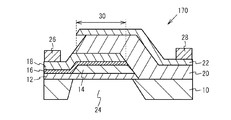
図1は、実施例1に係る圧電薄膜共振器を示す断面図である。図1のように、実施例1の圧電薄膜共振器100は、例えばシリコン(Si)基板からなる基板10上に、付加膜12が設けられている。なお、基板10は、Si基板以外にも、石英基板、ガラス基板、セラミック基板、又はガリウム砒素(GaAs)基板等を用いてもよい。付加膜12上に、温度補償膜として機能する酸化シリコン膜14が設けられている。付加膜12は、例えば酸化シリコン膜14の下面全面に設けられている。付加膜12は、例えば金属膜であり、例えば酸化シリコン膜14よりも高い音響インピーダンスを有する膜である。付加膜12は、例えばクロム(Cr)膜である。酸化シリコン膜14は、例えばフッ素(F)がドープされた酸化シリコン(SiOF)膜である。
FIG. 1 is a cross-sectional view illustrating the piezoelectric thin film resonator according to the first embodiment. As shown in FIG. 1, the piezoelectric
酸化シリコン膜14上に、酸素を含まない絶縁膜16が設けられている。酸素を含まない絶縁膜16は、例えば酸化シリコン膜14の上面全面に設けられている。酸素を含まない絶縁膜16は、例えば窒化シリコン(SiN)膜である。酸素を含まない絶縁膜16の厚さは、酸化シリコン膜14よりも薄くなっている。酸素を含まない絶縁膜16上に、下部電極18が設けられている。下部電極18は、例えばルテニウム(Ru)膜である。酸化シリコン膜14と下部電極18とは、その間に介在する酸素を含まない絶縁膜16によって、互いに接していない。また、付加膜12と下部電極18とは、その間に介在する酸化シリコン膜14及び酸素を含まない絶縁膜16によって、互いに接してなく、短絡していない。したがって、付加膜12は、弾性波の励振に対して電気的に寄与する膜ではない。
An insulating
下部電極18及び基板10上に、(002)方向を主軸とする窒化アルミニウム(AlN)膜からなる圧電膜20が設けられている。なお、圧電膜20は、AlN膜以外にも、酸化亜鉛(ZnO)、チタン酸ジルコン酸鉛(PZT)、又はチタン酸鉛(PbTiO3)等を用いてもよい。また、圧電膜20は、AlNを主成分とし、共振特性の向上又は圧電性の向上のために他の元素を含んでいてもよい。例えば、ドープ元素にスカンジウム(Sc)、マグネシウム(Mg)、ハフニウム(Hf)、ジルコニウム(Zr)、チタン(Ti)を用いることで、圧電膜20の圧電性を向上でき、圧電薄膜共振器の実効的電気機械結合係数を向上できる。
On the
下部電極18と対向する領域(共振領域30)を有するように、圧電膜20上に上部電極22が設けられている。上部電極22は、例えばRu膜である。共振領域30を含むように、基板10を貫通する空隙24が設けられている。共振領域30は、例えば楕円形状を有し、厚み縦振動モードの弾性波が共振する領域である。なお、共振領域30は、多角形状等、楕円形状以外であってもよい。
An
下部電極18の上面に接して第1電極パッド26が設けられ、上部電極22の上面に接して第2電極パッド28が設けられている。第1電極パッド26と第2電極パッド28とは、例えば金(Au)パッドである。
A
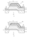
ここで、実施例1の圧電薄膜共振器の効果を説明するにあたり、比較例1及び比較例2の圧電薄膜共振器に対して発明者が行った高温信頼性試験(100℃、1000時間)について説明する。図2(a)及び図2(b)は、比較例1及び比較例2に係る圧電薄膜共振器を示す断面図である。 Here, in describing the effect of the piezoelectric thin film resonator of Example 1, the high temperature reliability test (100 ° C., 1000 hours) conducted by the inventors on the piezoelectric thin film resonators of Comparative Example 1 and Comparative Example 2 was performed. explain. 2A and 2B are cross-sectional views showing piezoelectric thin film resonators according to Comparative Example 1 and Comparative Example 2. FIG.
図2(a)のように、比較例1の圧電薄膜共振器は、Si基板310上に、厚さ100nmのCr膜からなる付加膜312が設けられている。付加膜312上に、厚さ200nmで、F濃度が9atm%のSiOF膜からなる酸化シリコン膜314が設けられている。酸化シリコン膜314上に、厚さ160nmのRu膜からなる下部電極318が設けられている。下部電極318及び基板310上に、厚さ1200nmのAlN膜からなる圧電膜320が設けられている。圧電膜320上に、厚さ230nmのRu膜からなる上部電極322が設けられている。共振領域330を含むように、基板310を貫通する空隙324が設けられている。また、下部電極318上及び上部電極322上にはそれぞれ、Auパッドからなる第1電極パッド326及び第2電極パッド328が設けられている。
As shown in FIG. 2A, the piezoelectric thin film resonator of Comparative Example 1 is provided with an
図2(b)のように、比較例2の圧電薄膜共振器は、下部電極318が、厚さ100nmのCr膜からなる第1膜318aと厚さ160nmのRu膜からなる第2膜318bとが積層された金属膜である点で、比較例1の圧電薄膜共振器と異なっている。その他の構成は、比較例1の図2(a)と同じであるため、説明を省略する。
As shown in FIG. 2B, in the piezoelectric thin film resonator of Comparative Example 2, the
図3(a)及び図3(b)は、高温信頼性試験の前後における比較例1及び比較例2の圧電薄膜共振器の反射特性のスミスチャートである。図3(a)及び図3(b)において、高温信頼性試験前を実線で示し、高温信頼性試験後を破線で示している。 FIGS. 3A and 3B are Smith charts of the reflection characteristics of the piezoelectric thin film resonators of Comparative Example 1 and Comparative Example 2 before and after the high temperature reliability test. 3A and 3B, the solid line before the high temperature reliability test is shown by a solid line, and the broken line after the high temperature reliability test is shown.
図3(a)のように、比較例1の圧電薄膜共振器では、高温信頼性試験によって特性が劣化した。例えば、高温信頼性試験前での共振Q値は1090、反共振Q値は933であったのに対し、高温信頼性試験後では、共振Q値が700、反共振Q値が829と劣化した。一方、図3(b)のように、比較例2の圧電薄膜共振器では、高温信頼性試験後も特性の劣化は見られるものの、比較例1の圧電薄膜共振器と比較して、特性の劣化は抑制された。例えば、高温信頼性試験前の共振Q値は1014、反共振Q値は788であり、高温信頼性試験後の共振Q値は691、反共振Q値は721であった。 As shown in FIG. 3A, in the piezoelectric thin film resonator of Comparative Example 1, the characteristics were deteriorated by the high temperature reliability test. For example, the resonance Q value before the high temperature reliability test was 1090 and the antiresonance Q value was 933, whereas after the high temperature reliability test, the resonance Q value was 700 and the antiresonance Q value was 829. . On the other hand, as shown in FIG. 3B, although the piezoelectric thin film resonator of Comparative Example 2 shows deterioration in characteristics even after the high-temperature reliability test, the characteristic is lower than that of the piezoelectric thin film resonator of Comparative Example 1. Degradation was suppressed. For example, the resonance Q value before the high temperature reliability test was 1014 and the antiresonance Q value was 788, the resonance Q value after the high temperature reliability test was 691, and the antiresonance Q value was 721.
比較例1の圧電薄膜共振器において、高温信頼性試験によって特性が劣化したのは以下の理由によるものと考えられる。即ち、下部電極318であるRu膜は酸化し易いため、下部電極318(Ru膜)と酸化シリコン膜314とが接して設けられることで、高温信頼性試験において、酸化シリコン膜314の膜中の酸素によって下部電極318が酸化し、その結果、特性が劣化したものと考えられる。また、高温信頼性試験後に電極抵抗が増大していることが確認され、これからも、下部電極318が酸化していることが認められる。一方、比較例2の圧電薄膜共振器では、下部電極318がCr膜からなる第1膜318aとRu膜からなる第2膜318bとの積層膜であるため、酸化シリコン膜314は第1膜318a(Cr膜)に接している。Cr膜は酸化され難いため、下部電極318の酸化が抑制され、その結果、特性の劣化が抑えられたものと考えられる。
In the piezoelectric thin film resonator of Comparative Example 1, the characteristics were degraded by the high temperature reliability test for the following reason. That is, since the Ru film which is the
このことを踏まえると、実施例1の圧電薄膜共振器100では、図1のように、酸化シリコン膜14と下部電極18との間に酸素を含まない絶縁膜16が設けられている。これにより、酸化シリコン膜14の膜中の酸素による下部電極18の酸化を抑制することができる。また、図2(b)の比較例2のように、下部電極318の第1膜318aに酸化され難い金属膜を用いたとしても多少の酸化は起こり得るが、実施例1のように、酸化シリコン膜14と下部電極18との間に酸素を含まない絶縁膜16を設けることで、下部電極18の酸化をより抑制できる。また、酸化シリコン膜14は吸湿性を示す材料であり、例えば高温信頼性試験において、水分を吸収して膜質が変化(例えばQ値が劣化)することが起こるが、実施例1では、酸化シリコン膜14下(即ち、酸素を含まない絶縁膜16とは反対側)に、Cr膜からなる付加膜12が設けられている。このため、酸化シリコン膜14が水分を吸収することを抑制できる。これらのことから、実施例1の圧電薄膜共振器100によれば、特性の劣化を抑制することができる。
In view of this, in the piezoelectric
また、実施例1の圧電薄膜共振器100では、付加膜12に、酸化シリコン膜14よりも音響インピーダンスの高い膜を用いている。これにより、温度補償膜として機能する酸化シリコン膜14は弾性波エネルギーのより大きな部分に設けられることになるため、温度特性を改善するための酸化シリコン膜14の厚さを薄くすることができ、その結果、共振特性の向上が図れる。なお、酸化シリコン膜14がSiOF膜からなる場合、SiOF膜よりも音響インピーダンスが高い金属膜として、Cr膜以外にも、例えばRu膜やCrとRuの積層膜等が挙げられる。
In the piezoelectric
このように、付加膜12は、酸化シリコン膜14よりも耐湿性に優れ且つ酸化シリコン膜14よりも音響インピーダンスの高い膜であることが好ましい。
As described above, it is preferable that the
また、実施例1の圧電薄膜共振器100では、酸素を含まない絶縁膜16の膜厚は、酸化シリコン膜14よりも薄くなっている。酸素を含まない絶縁膜16が厚いほど、酸化シリコン膜14による温度補償の効果が小さくなるが、酸素を含まない絶縁膜16の膜厚を酸化シリコン膜14よりも薄くすることで、良好な温度補償効果を得ることができる。
In the piezoelectric
また、実施例1の圧電薄膜共振器100では、酸化シリコン膜14がSiOF膜であるため、酸化シリコン膜14の弾性定数の温度係数を大きくでき、その結果、酸化シリコン膜14の厚さを薄くできる。これにより、共振特性の向上が図れる。また、SiOF膜は特に吸湿し易い性質を有するが、実施例1では、酸化シリコン膜14下に付加膜12が設けられているため、酸化シリコン膜14がSiOF膜である場合でも水分の吸収を抑制することができる。
In the piezoelectric
なお、実施例1では、酸化シリコン膜14がSiOF膜である場合を例に示したが、フッ素(F)以外の他の元素がドープされている場合でもよいし、シリコンと酸素以外の他の元素がドープされていない二酸化シリコン(SiO2)膜の場合でもよい。例えば、酸化シリコン膜14は、酸化シリコンを主成分とし、フッ素(F)、水素(H)、CH3、CH2、塩素(Cl)、炭素(C)、窒素(N)、リン(P)、及び硫黄(S)のうちの少なくとも1つ又は2つ以上の元素がドープされていてもよい。このように、酸化シリコン膜14に他の元素がドープされることで、酸化シリコン膜14の弾性定数の温度係数を大きくできるため、酸化シリコン膜14の厚さを薄くでき、その結果、共振特性の向上が図れる。
In the first embodiment, the case where the
なお、実施例1では、下部電極18がRu膜である場合を例に示したが、その他の金属膜の場合でもよい。例えば、下部電極18は、クロム(Cr)、ルテニウム(Ru)、アルミニウム(Al)、チタン(Ti)、銅(Cu)、モリブデン(Mo)、タングステン(W)、タンタル(Ta)、白金(Pt)、ロジウム(Rh)、又はイリジウム(Ir)等の単層膜又はこれらの積層膜の場合でもよい。また、下部電極18が酸化し易い金属である場合に、実施例1のように、酸化シリコン膜14と下部電極18との間に酸素を含まない絶縁膜16を設けることが好ましい。上述した金属のうち、酸化し易い金属として、Al、Cu、Ruが挙げられる。上部電極22も、Ru膜以外の金属膜の場合でも良く、例えば、Cr、Ru、Al、Ti、Cu、Mo、W、Ta、Pt、Rh、又はIr等の単層膜又はこれらの積層膜を用いてもよい。
In the first embodiment, the case where the
なお、実施例1では、酸化シリコン膜14と下部電極18との間の酸素を含まない絶縁膜16が、SiN膜の場合を例に示したがこれに限られない。例えば、AlN膜等の窒化系絶縁膜の場合でもよいし、下部電極18の酸化が起こらない程度の酸素、例えば不純物としての酸素、を含んでいる場合でもよい。
In the first embodiment, the case where the insulating
図4(a)及び図4(b)は、実施例1の変形例1及び実施例1の変形例2に係る圧電薄膜共振器を示す断面図である。図4(a)のように、実施例1の変形例1の圧電薄膜共振器110は、酸化シリコン膜14の側面のうちの圧電膜20で覆われていない側面に絶縁膜32が設けられている。絶縁膜32は、例えば圧電膜20で覆われていない酸化シリコン膜14の側面全面に設けられている。絶縁膜32は、酸化シリコン膜14とは異なる材料からなり、例えば窒化シリコン(SiN)膜からなる。その他の構成は、実施例1の図1と同じであるため、説明を省略する。
4A and 4B are cross-sectional views illustrating the piezoelectric thin film resonator according to the first modification of the first embodiment and the second modification of the first embodiment. As shown in FIG. 4A, the piezoelectric
実施例1の変形例1の圧電薄膜共振器110では、圧電膜20で覆われていない酸化シリコン膜14の側面に絶縁膜32が設けられている。これにより、酸化シリコン膜14が水分を吸収することをより抑制することができ、特性の劣化をより抑制することができる。
In the piezoelectric
絶縁膜32は、圧電膜20で覆われていない酸化シリコン膜14の側面全面に設けられている場合が好ましいが、圧電膜20で覆われていない酸化シリコン膜14の側面の少なくとも一部に設けられることで、酸化シリコン膜14の水分の吸収を抑制する効果は得られる。また、絶縁膜32は、SiN膜以外の絶縁膜を用いてもよく、酸化シリコン膜14よりも耐湿性に優れた膜を用いることが好ましい。また、絶縁膜32の材料に、酸素を含まない絶縁膜16と同じ材料を選択することで、酸素を含まない絶縁膜16と絶縁膜32とを同時に形成することが可能となる。
The insulating
図4(b)のように、実施例1の変形例2の圧電薄膜共振器120は、酸素を含まない絶縁膜16が酸化シリコン膜14の側面のうちの圧電膜20で覆われた側面に延在して設けられている。酸素を含まない絶縁膜16は、例えば圧電膜20で覆われた酸化シリコン膜14の側面全面に設けられている。その他の構成は、実施例1の変形例1の図4(a)と同じであるため、説明を省略する。
As shown in FIG. 4B, the piezoelectric
実施例1の変形例2の圧電薄膜共振器120では、酸素を含まない絶縁膜16が圧電膜20で覆われた酸化シリコン膜14の側面に延在して設けられている。これにより、例えば高温信頼性試験において、酸化シリコン膜14の膜中の酸素によって圧電膜20が酸化されることを抑制できるため、特性の劣化を抑制できる。
In the piezoelectric
酸素を含まない絶縁膜16は、圧電膜20で覆われた酸化シリコン膜14の側面全面に設けられている場合が好ましいが、圧電膜20で覆われた酸化シリコン膜14の側面の少なくとも一部に設けられることで、圧電膜20の酸化を抑制する効果は得られる。
The insulating
実施例1は、付加膜が金属膜である場合の例であったが、実施例2では、絶縁膜である場合の例について説明する。図5(a)及び図5(b)は、実施例2及び実施例2の変形例1に係る圧電薄膜共振器を示す断面図である。 The first embodiment is an example in which the additional film is a metal film. In the second embodiment, an example in which the additional film is an insulating film will be described. FIG. 5A and FIG. 5B are cross-sectional views illustrating the piezoelectric thin film resonators according to the second embodiment and the first modification of the second embodiment.
図5(a)のように、実施例2の圧電薄膜共振器130は、酸化シリコン膜14下に設けられている付加膜12aは、酸化シリコン膜14とは異なる材料からなる絶縁膜であり、例えば窒化シリコン(SiN)膜である。その他の構成は、実施例1の変形例1の図4(a)と同じであるため、説明を省略する。
As shown in FIG. 5A, in the piezoelectric
実施例2の圧電薄膜共振器130のように、酸化シリコン膜14下に設けられる付加膜12aは、Cr膜等の金属膜である場合に限らず、SiN膜等の絶縁膜である場合でもよい。この場合でも、酸化シリコン膜14が水分を吸収することを抑制でき、特性の劣化を抑制できる。
Like the piezoelectric
また、絶縁膜からなる付加膜12aは、実施例1のような金属膜からなる付加膜12に比べて、優れた耐湿性を得ることができる。このため、実施例2は、実施例1に比べて、付加膜の厚さが同じ場合における酸化シリコン膜14の水分吸収をより抑制できる。言い換えると、酸化シリコン膜14の水分吸収を抑制するための付加膜の厚さを薄くすることができる。
Further, the
また、実施例2の圧電薄膜共振器130では、圧電膜20で覆われていない酸化シリコン膜14の側面に絶縁膜32が設けられているので、酸化シリコン膜14が水分を吸収することをより抑制でき、特性の劣化をより抑制できる。
Further, in the piezoelectric
なお、実施例2の圧電薄膜共振器130では、付加膜12aがSiN膜である場合を例に示したが、その他の絶縁膜の場合でもよく、酸化シリコン膜14よりも耐湿性に優れた絶縁膜である場合が好ましい。また、付加膜12aは、酸化シリコン膜14よりも音響インピーダンスの高い絶縁膜である場合が好ましい。例えば酸化シリコン膜14がSiOF膜からなる場合、SiOF膜よりも音響インピーダンスが高い絶縁膜として、窒化アルミニウム(AlN)膜及び酸化アルミニウム(Al2O3)膜等が挙げられる。
In the piezoelectric
図5(b)のように、実施例2の変形例1の圧電薄膜共振器140は、酸素を含まない絶縁膜16が酸化シリコン膜14の側面のうちの圧電膜20で覆われた側面に延在して設けられている。その他の構成は、実施例2の図5(a)と同じであるため、説明を省略する。
As shown in FIG. 5B, the piezoelectric
実施例2の変形例1の圧電薄膜共振器140では、酸素を含まない絶縁膜16が圧電膜20で覆われた酸化シリコン膜14の側面に延在して設けられているので、酸化シリコン膜14の膜中の酸素によって圧電膜20が酸化されることを抑制できる。
In the piezoelectric
実施例3では、付加膜が金属膜と絶縁膜の積層膜である場合の例について説明する。図6(a)及び図6(b)は、実施例3及び実施例3の変形例1に係る圧電薄膜共振器を示す断面図である。 In Example 3, an example in which the additional film is a laminated film of a metal film and an insulating film will be described. FIGS. 6A and 6B are cross-sectional views illustrating the piezoelectric thin film resonators according to the third embodiment and the first modification of the third embodiment.
図6(a)のように、実施例3の圧電薄膜共振器150では、酸化シリコン膜14下に設けられている付加膜12bは、金属膜からなる第1膜13aと、酸素を含まない絶縁膜からなる第2膜13bと、が積層された積層膜である。第1膜13aは、例えばRu膜であり、第2膜13bは、例えば窒化シリコン(SiN)膜である。その他の構成は、実施例1の変形例1の図4(a)と同じであるため、説明を省略する。
As shown in FIG. 6A, in the piezoelectric
実施例3の圧電薄膜共振器150のように、付加膜12bが、酸化シリコン膜14側から酸素を含まない絶縁膜の第2膜13bと金属膜の第1膜13aとが順に積層された積層膜である場合でもよい。この場合でも、酸化シリコン膜14が水分を吸収することを抑制でき、特性の劣化を抑制できる。
Like the piezoelectric
また、実施例1では、金属膜からなる付加膜12が酸化シリコン膜14の膜中の酸素によって酸化されて、特性の劣化が生じる恐れがある。例えば、付加膜12にRu膜のような酸化され易い金属膜を用いる場合に、酸化による特性の劣化が起こり易い。一方、実施例3では、付加膜12bは、酸化シリコン膜14側から酸素を含まない絶縁膜である第2膜13bと金属膜である第1膜13aとが積層された積層膜となっている。酸化シリコン膜14と金属膜である第1膜13aとの間に、酸素を含まない絶縁膜である第2膜13bが介在しているため、第1膜13aの酸化が抑制でき、特性の劣化を抑制することができる。
Further, in the first embodiment, the
また、実施例3の圧電薄膜共振器150では、圧電膜20で覆われていない酸化シリコン膜14の側面に絶縁膜32が設けられているので、酸化シリコン膜14が水分を吸収することをより抑制でき、特性の劣化をより抑制できる。
Further, in the piezoelectric
なお、実施例3の圧電薄膜共振器150では、付加膜12bの第1膜13aがRu膜である場合を例に示したが、Cr膜等のその他の金属膜の場合でもよい。付加膜12bの第2膜13bがSiN膜である場合を例に示したが、窒化アルミニウム(AlN)膜等の窒化系絶縁膜等、酸素を含まない絶縁膜であればその他の絶縁膜の場合でもよい。
In the piezoelectric
図6(b)のように、実施例3の変形例1の圧電薄膜共振器160は、酸素を含まない絶縁膜16が酸化シリコン膜14の側面のうちの圧電膜20で覆われた側面に延在して設けられている。その他の構成は、実施例3の図6(a)と同じであるため、説明を省略する。
As shown in FIG. 6B, the piezoelectric
実施例3の変形例1の圧電薄膜共振器160では、酸素を含まない絶縁膜16が圧電膜20で覆われた酸化シリコン膜14の側面に延在して設けられているので、酸化シリコン膜14の膜中の酸素によって圧電膜20が酸化されることを抑制できる。
In the piezoelectric
図7は、実施例4に係る圧電薄膜共振器を示す断面図である。図7のように、実施例4の圧電薄膜共振器170は、下部電極18の上面に接して設けられた第1電極パッド26下における酸化シリコン膜14が除去されていて、第1電極パッド26下には酸化シリコン膜14が設けられていない。酸化シリコン膜14と下部電極18との間に設けられた酸素を含まない絶縁膜16は、酸化シリコン膜14の側面を覆って第1電極パッド26下にまで延在している。このため、下部電極18と付加膜12とは接してなく、短絡していない。その他の構成は、実施例1の図1と同じであるため、説明を省略する。
FIG. 7 is a cross-sectional view illustrating the piezoelectric thin film resonator according to the fourth embodiment. As shown in FIG. 7, in the piezoelectric
実施例4の圧電薄膜共振器では、第1電極パッド26下に、酸化シリコン膜14が設けられていない。これにより、電気的容量を増加させる絶縁膜を除去できるため、直列成分の不要な容量を低減することができ、その結果、特性の劣化を抑制することができる。
In the piezoelectric thin film resonator according to the fourth embodiment, the
図8(a)から図9(b)は、実施例4の変形例1から実施例4の変形例5に係る圧電薄膜共振器を示す断面図である。図8(a)のように、実施例4の変形例1に係る圧電薄膜共振器180は、酸素を含まない絶縁膜16が酸化シリコン膜14の側面のうちの圧電膜20で覆われた側面に延在して設けられている。その他の構成は、実施例4の図7と同じであるため、説明を省略する。
FIG. 8A to FIG. 9B are cross-sectional views showing piezoelectric thin film resonators according to the first modification of the fourth embodiment to the fifth modification of the fourth embodiment. As shown in FIG. 8A, the piezoelectric
実施例4の変形例1の圧電薄膜共振器180では、酸素を含まない絶縁膜16が圧電膜20で覆われた酸化シリコン膜14の側面に延在して設けられているので、酸化シリコン膜14の膜中の酸素によって圧電膜20が酸化されることを抑制できる。
In the piezoelectric
図8(b)のように、実施例4の変形例2に係る圧電薄膜共振器190では、酸化シリコン膜14下に、金属膜からなる付加膜12に代わって、酸化シリコン膜14とは異なる材料の絶縁膜からなる付加膜12aが設けられている。その他の構成は、実施例4の図7と同じであるため、説明を省略する。
As shown in FIG. 8B, the piezoelectric
実施例4の変形例2の圧電薄膜共振器190のように、付加膜12aは、窒化シリコン膜等の酸化シリコン膜14とは異なる材料の絶縁膜である場合でもよい。この場合でも、酸化シリコン膜14が水分を吸収することを抑制でき、特性の劣化を抑制できる。
As in the piezoelectric
図8(c)のように、実施例4の変形例3に係る圧電薄膜共振器200は、酸素を含まない絶縁膜16が酸化シリコン膜14の側面のうちの圧電膜20で覆われた側面に延在して設けられている。その他の構成は、実施例4の変形例2の図8(b)と同じであるため、説明を省略する。
As shown in FIG. 8C, the piezoelectric
実施例4の変形例3の圧電薄膜共振器200では、酸素を含まない絶縁膜16が圧電膜20で覆われた酸化シリコン膜14の側面に延在して設けられているので、酸化シリコン膜14の膜中の酸素によって圧電膜20が酸化されることを抑制できる。
In the piezoelectric
図9(a)のように、実施例4の変形例4に係る圧電薄膜共振器210では、酸化シリコン膜14下に、金属膜からなる付加膜12に代わって、金属膜からなる第1膜13aと酸素を含まない絶縁膜からなる第2膜13bとが積層された積層膜からなる付加膜12bが設けられている。その他の構成は、実施例4の図7と同じであるため、説明を省略する。
As shown in FIG. 9A, in the piezoelectric
実施例4の変形例4の圧電薄膜共振器210のように、付加膜12bが、酸化シリコン膜14側から酸素を含まない絶縁膜の第2膜13bと金属膜の第1膜13aとが順に積層された積層膜である場合でもよい。この場合でも、酸化シリコン膜14が水分を吸収することを抑制でき、特性の劣化を抑制できる。また、酸化シリコン膜14と第1膜13aとの間に酸素を含まない絶縁膜の第2膜13bが設けられていることで、第1膜13aが酸化することを抑制できる。
As in the piezoelectric
図9(b)のように、実施例4の変形例5に係る圧電薄膜共振器220は、酸素を含まない絶縁膜16が酸化シリコン膜14の側面のうちの圧電膜20で覆われた側面に延在して設けられている。その他の構成は、実施例4の変形例4の図9(a)と同じであるため、説明を省略する。
As illustrated in FIG. 9B, the piezoelectric
実施例4の変形例5の圧電薄膜共振器220では、酸素を含まない絶縁膜16が圧電膜20で覆われた酸化シリコン膜14の側面に延在して設けられているので、酸化シリコン膜14の膜中の酸素によって圧電膜20が酸化されることを抑制できる。
In the piezoelectric
実施例1から実施例4では、付加膜及び酸化シリコン膜が下部電極の圧電膜に対して反対側に設けられていたが、実施例5は、付加膜及び酸化シリコン膜が上部電極の圧電膜に対して反対側に設けられた場合の例である。図10(a)及び図10(b)は、実施例5及び実施例5の変形例1に係る圧電薄膜共振器を示す断面図である。 In Example 1 to Example 4, the additional film and the silicon oxide film were provided on the opposite side to the piezoelectric film of the lower electrode. However, in Example 5, the additional film and the silicon oxide film were the piezoelectric film of the upper electrode. It is an example at the time of being provided in the opposite side with respect to. FIGS. 10A and 10B are cross-sectional views illustrating the piezoelectric thin film resonators according to the fifth embodiment and the first modification of the fifth embodiment.
図10(a)のように、実施例5の圧電薄膜共振器230は、例えばSi基板からなる基板10上に、例えばRu膜からなる下部電極18が設けられている。下部電極18及び基板10上に、例えばAlN膜からなる圧電膜20が設けられている。下部電極18と対向する共振領域30を有するように、圧電膜20上に、例えばRu膜からなる上部電極22が設けられている。共振領域30を含むように、基板10を貫通する空隙24が設けられている。
As shown in FIG. 10A, in the piezoelectric
上部電極22上に、例えば窒化シリコン(SiN)膜からなる酸素を含まない絶縁膜16が設けられている。酸素を含まない絶縁膜16上に、温度補償膜として機能する酸化シリコン膜14が設けられている。酸化シリコン膜14は、例えばSiOF膜である。酸化シリコン膜14上に、例えばCr膜からなる付加膜12が設けられている。
On the
下部電極18の上面に接して第1電極パッド26が設けられ、上部電極22の上面に接して第2電極パッド28が設けられている。第1電極パッド26と第2電極パッド28とは、例えば金(Au)パッドである。
A
実施例5の圧電薄膜共振器230では、上部電極22の圧電膜20とは反対側に設けられた酸化シリコン膜14と上部電極22との間に酸素を含まない絶縁膜16が設けられている。これにより、酸化シリコン膜14の膜中の酸素による上部電極22の酸化を抑制することができる。また、酸化シリコン膜14上(即ち、酸素を含まない絶縁膜16とは反対側)に、付加膜12が設けられている。このため、酸化シリコン膜14が水分を吸収することを抑制できる。これらのことから、実施例5の圧電薄膜共振器230によれば、特性の劣化を抑制できる。
In the piezoelectric
酸化シリコン膜14の水分の吸収を抑制する点から、付加膜12は、酸化シリコン膜14の上面全面に設けられている場合が好ましく、酸化シリコン膜14の側面にも設けられている場合が好ましい。
From the viewpoint of suppressing moisture absorption of the
実施例1及び実施例5のように、酸化シリコン膜14は、下部電極18及び上部電極22の少なくとも一方の圧電膜20に対して反対側に設けられていればよく、下部電極18及び上部電極22の両方の圧電膜20に対して反対側に設けられていてもよい。
As in the first and fifth embodiments, the
図10(b)のように、実施例5の変形例1の圧電薄膜共振器240は、酸化シリコン膜14の側面のうちの付加膜12で覆われていない側面に絶縁膜34が設けられている。絶縁膜34は、例えば付加膜12で覆われていない酸化シリコン膜14の側面全面に設けられている。絶縁膜34は、酸化シリコン膜14とは異なる材料からなり、例えば窒化シリコン(SiN)膜からなる。その他の構成は、実施例5の図10(a)と同じであるため、説明を省略する。
As illustrated in FIG. 10B, the piezoelectric
実施例5の変形例1の圧電薄膜共振器240では、付加膜12で覆われていない酸化シリコン膜14の側面に絶縁膜34が設けられている。これにより、酸化シリコン膜14の水分の吸収をより抑制することができ、特性の劣化をより抑制することができる。
In the piezoelectric
絶縁膜34は、付加膜12で覆われていない酸化シリコン膜14の側面全面に設けられている場合が好ましいが、付加膜12で覆われていない酸化シリコン膜14の側面の少なくとも一部に設けられることで、酸化シリコン膜14の水分の吸収を抑制する効果は得られる。また、絶縁膜34は、SiN膜以外の絶縁膜を用いてもよく、酸化シリコン膜14よりも耐湿性に優れた膜を用いることが好ましい。
The insulating
図11(a)及び図11(b)は、実施例6及び実施例6の変形例1に係る圧電薄膜共振器を示す断面図である。図11(a)のように、実施例6の圧電薄膜共振器250は、酸化シリコン膜14上に設けられている付加膜12aが、酸化シリコン膜14とは異なる材料からなる絶縁膜であり、例えば窒化シリコン(SiN)膜である。その他の構成は、実施例5の図10(a)と同じであるため、説明を省略する。
FIGS. 11A and 11B are cross-sectional views illustrating the piezoelectric thin film resonators according to the sixth embodiment and the first modification of the sixth embodiment. As shown in FIG. 11A, in the piezoelectric
実施例6の圧電薄膜共振器250のように、酸化シリコン膜14の酸素を含まない絶縁膜16に対して反対側に設けられる付加膜12aは、SiN膜等の絶縁膜である場合でもよい。この場合でも、酸化シリコン膜14が水分を吸収することを抑制でき、特性の劣化を抑制できる。
As in the piezoelectric
図11(b)のように、実施例6の変形例1の圧電薄膜共振器260は、酸化シリコン膜14の側面のうちの付加膜12aで覆われていない側面に絶縁膜34が設けられている。その他の構成は、実施例6の図11(a)と同じであるため、説明を省略する。
As shown in FIG. 11B, the piezoelectric
実施例6の変形例1の圧電薄膜共振器260では、付加膜12aで覆われていない酸化シリコン膜14の側面に絶縁膜34が設けられているので、酸化シリコン膜14が水分を吸収することをより抑制でき、特性の劣化をより抑制できる。
In the piezoelectric
なお、実施例5及び実施例6のように、酸化シリコン膜が上部電極の圧電膜に対して反対側に設けられている場合でも、実施例3の図6(a)のように、酸化シリコン膜側から絶縁膜からなる第2膜13bと金属膜からなる第1膜13aとが積層された付加膜12bを用いてもよい。
Even when the silicon oxide film is provided on the opposite side to the piezoelectric film of the upper electrode as in Example 5 and Example 6, as shown in FIG. An
実施例7及び実施例7の変形例1は、空隙の構成を変えた例である。図12(a)及び図12(b)は、実施例7及び実施例7の変形例1に係る圧電薄膜共振器を示す断面図である。図12(a)のように、実施例7の圧電薄膜共振器270では、共振領域30における基板10に形成された空隙24aが、基板10を貫通してなく、基板10の上面に窪みの形状として形成されている。その他の構成は、実施例1の図1と同じであるため、説明を省略する。
The seventh embodiment and the first modification of the seventh embodiment are examples in which the structure of the gap is changed. 12A and 12B are cross-sectional views illustrating the piezoelectric thin film resonators according to the seventh embodiment and the first modification of the seventh embodiment. As shown in FIG. 12A, in the piezoelectric
図12(b)のように、実施例7の変形例1の圧電薄膜共振器280では、基板10に空隙は形成されてなく、付加膜12が、基板10の上面との間にドーム形状の膨らみを有する空隙24bが形成されるように、基板10上に設けられている。ドーム状の膨らみとは、例えば空隙24bの周辺では空隙24bの高さが低く、空隙24bの中央ほど空隙24bの高さが高くなるような形状の膨らみである。その他の構成は、実施例1の図1と同じであるため、説明を省略する。
As shown in FIG. 12B, in the piezoelectric
なお、実施例7及び実施例7の変形例1の圧電薄膜共振器では、実施例1の圧電薄膜共振器の空隙24の形状を、空隙24a、24bの形状に変えた場合を例に示したが、実施例1の変形例1から実施例6の変形例1の圧電薄膜共振器の空隙24を、実施例7及び実施例7の変形例1の空隙24a、24bに変えてもよい。
In the piezoelectric thin film resonator according to the seventh example and the first modification of the seventh example, the shape of the
実施例8は、空隙の代わりに音響反射膜を設けた例である。図13は、実施例8に係る圧電薄膜共振器を示す断面図である。図13のように、実施例8の圧電薄膜共振器290では、共振領域30の付加膜12の下面に音響反射膜40が設けられている。音響反射膜40は、圧電膜20を伝搬する弾性波を反射する膜であり、音響インピーダンスの低い膜42と音響インピーダンスの高い膜44とが交互に設けられている。音響インピーダンスの低い膜42と高い膜44の膜厚は、λ/4(λは弾性波の波長)程度である。音響インピーダンスの低い膜42と高い膜44の積層数は任意に設定できる。なお、付加膜12と酸化シリコン膜14との膜厚は、λ/4よりも十分薄いため、音響反射膜としては機能してない。その他の構成は、実施例1の図1と同じであるため、説明を省略する。
Example 8 is an example in which an acoustic reflection film is provided instead of the gap. FIG. 13 is a cross-sectional view illustrating the piezoelectric thin film resonator according to the eighth embodiment. As shown in FIG. 13, in the piezoelectric
なお、実施例8の圧電薄膜共振器では、実施例1の圧電薄膜共振器の空隙24の代わりに音響反射膜40を設けた場合を例に示したが、実施例1の変形例1から実施例6の変形例1の圧電薄膜共振器の空隙24の代わりに音響反射膜40を設けてもよい。
In the piezoelectric thin film resonator according to the eighth embodiment, the acoustic reflection film 40 is provided instead of the
このように、圧電薄膜共振器は、実施例1から実施例7の変形例1のように、共振領域30における下部電極18下に空隙24〜24bが設けられたFBAR構造の場合でもよい。実施例8のように、共振領域30における下部電極18下に音響反射膜40が設けられたSMR(Solidly Mounted Resonator)構造の場合でもよい。
As described above, the piezoelectric thin film resonator may have an FBAR structure in which the
実施例9は、実施例1から実施例8の圧電薄膜共振器をフィルタに用いた例である。図14は、実施例9に係るラダー型フィルタを示す回路図である。図14のように、ラダー型フィルタは、1又は複数の直列共振器S1〜S3、及び、1又は複数の並列共振器P1〜P2を備えている。直列共振器S1〜S3は、入出力端子T1とT2との間に直列に接続されている。並列共振器P1〜P2は、入出力端子T1とT2との間に並列に接続されている。直列共振器S1〜S3及び並列共振器P1〜P2の少なくとも1つを、実施例1から実施例8に例示した圧電薄膜共振器とすることができる。 Example 9 is an example in which the piezoelectric thin film resonator of Examples 1 to 8 is used as a filter. FIG. 14 is a circuit diagram illustrating a ladder filter according to the ninth embodiment. As shown in FIG. 14, the ladder filter includes one or more series resonators S1 to S3 and one or more parallel resonators P1 to P2. The series resonators S1 to S3 are connected in series between the input / output terminals T1 and T2. The parallel resonators P1 and P2 are connected in parallel between the input / output terminals T1 and T2. At least one of the series resonators S1 to S3 and the parallel resonators P1 to P2 can be the piezoelectric thin film resonator exemplified in the first to eighth embodiments.
以上、本発明の実施例について詳述したが、本発明はかかる特定の実施例に限定されるものではなく、特許請求の範囲に記載された本発明の要旨の範囲内において、種々の変形・変更が可能である。 Although the embodiments of the present invention have been described in detail above, the present invention is not limited to such specific embodiments, and various modifications and changes can be made within the scope of the gist of the present invention described in the claims. It can be changed.
10 基板
12、12a、12b 付加膜
13a 第1膜
13b 第2膜
14 酸化シリコン膜
16 酸素を含まない絶縁膜
18 下部電極
20 圧電膜
22 上部電極
24、24a、24b 空隙
26 第1電極パッド
28 第2電極パッド
30 共振領域
32 絶縁膜
34 絶縁膜
40 音響反射膜
42 音響インピーダンスの低い膜
44 音響インピーダンスの高い膜
100〜290 圧電薄膜共振器
10
Claims (12)
前記基板上に設けられた圧電膜と、
前記圧電膜の少なくとも一部を挟んで対向した下部電極及び上部電極と、
前記下部電極の前記圧電膜に対して反対側に設けられた酸化シリコン膜と、
前記下部電極と前記酸化シリコン膜との間に設けられた酸素元素を含まない絶縁材料を有する第1絶縁膜と、
前記酸化シリコン膜の前記第1絶縁膜に対して反対側に設けられ、前記酸化シリコン膜及び前記第1絶縁膜とは異なる材料である付加膜と、を備え、
前記圧電膜は、前記酸化シリコン膜上から前記酸化シリコン膜の側方に延在していて、
前記第1絶縁膜は、前記酸化シリコン膜の側面のうちの前記圧電膜で覆われた側面と前記圧電膜との間に延在している、弾性波デバイス。 A substrate,
A piezoelectric film provided on the substrate;
A lower electrode and an upper electrode facing each other across at least a part of the piezoelectric film;
A silicon oxide film provided on the opposite side with respect to the piezoelectric layer of the lower electrodes,
A first insulating film having an insulating material which does not contain the oxygen element which is provided between the silicon oxide film and the lower electrodes,
An additional film that is provided on the opposite side of the silicon oxide film with respect to the first insulating film and is made of a material different from the silicon oxide film and the first insulating film;
The piezoelectric film extends from the silicon oxide film to the side of the silicon oxide film,
The first insulating film is an acoustic wave device that extends between a side surface of the silicon oxide film covered with the piezoelectric film and the piezoelectric film .
前記基板上に設けられた圧電膜と、
前記圧電膜の少なくとも一部を挟んで対向した下部電極及び上部電極と、
前記下部電極及び前記上部電極の少なくとも一方の前記圧電膜に対して反対側に設けられたフッ素がドープされた酸化シリコン膜と、
前記下部電極及び前記上部電極の少なくとも一方と前記酸化シリコン膜との間に設けられた酸素元素を含まない絶縁材料を有する第1絶縁膜と、
前記酸化シリコン膜の前記第1絶縁膜に対して反対側に設けられ、前記酸化シリコン膜及び前記第1絶縁膜とは異なる材料である付加膜と、
前記酸化シリコン膜の側面のうちの前記圧電膜又は前記付加膜で覆われていない側面に設けられ、前記酸化シリコン膜とは異なる材料からなる第2絶縁膜と、を備える、弾性波デバイス。 A substrate,
A piezoelectric film provided on the substrate;
A lower electrode and an upper electrode facing each other across at least a part of the piezoelectric film;
A fluorine-doped silicon oxide film provided on the opposite side to the piezoelectric film of at least one of the lower electrode and the upper electrode ;
A first insulating film having an insulating material not containing an oxygen element and provided between at least one of the lower electrode and the upper electrode and the silicon oxide film;
An additional film which is provided on the opposite side of the silicon oxide film with respect to the first insulating film and is made of a material different from the silicon oxide film and the first insulating film;
An elastic wave device comprising: a second insulating film that is provided on a side surface of the silicon oxide film that is not covered with the piezoelectric film or the additional film, and is made of a material different from the silicon oxide film.
前記基板上に設けられた圧電膜と、
前記圧電膜の少なくとも一部を挟んで対向した下部電極及び上部電極と、
前記下部電極の前記圧電膜に対して反対側に設けられた酸化シリコン膜と、
前記下部電極と前記酸化シリコン膜との間に設けられた酸素元素を含まない絶縁材料を有する第1絶縁膜と、
前記酸化シリコン膜の前記第1絶縁膜に対して反対側に設けられ、前記酸化シリコン膜及び前記第1絶縁膜とは異なる材料である付加膜と、
前記下部電極の上面に接して設けられた電極パッドと、を備え、
前記電極パッド下には、前記酸化シリコン膜が設けられていない、弾性波デバイス。 A substrate,
A piezoelectric film provided on the substrate;
A lower electrode and an upper electrode facing each other across at least a part of the piezoelectric film;
A silicon oxide film provided on the opposite side to the piezoelectric film of the lower electrode;
A first insulating film having an insulating material not containing an oxygen element provided between the lower electrode and the silicon oxide film;
An additional film which is provided on the opposite side of the silicon oxide film with respect to the first insulating film and is made of a material different from the silicon oxide film and the first insulating film;
An electrode pad provided in contact with the upper surface of the lower electrode,
An acoustic wave device in which the silicon oxide film is not provided under the electrode pad.
前記基板上に設けられた圧電膜と、
前記圧電膜の少なくとも一部を挟んで対向した下部電極及び上部電極と、
前記下部電極及び前記上部電極の少なくとも一方の前記圧電膜に対して反対側に設けられた酸化シリコン膜と、
前記下部電極及び前記上部電極の少なくとも一方と前記酸化シリコン膜との間に設けられた酸素元素を含まない絶縁材料を有する第1絶縁膜と、
前記酸化シリコン膜の前記第1絶縁膜に対して反対側に設けられ、前記酸化シリコン膜及び前記第1絶縁膜とは異なる材料である金属膜からなる付加膜と、を備える、弾性波デバイス。 A substrate,
A piezoelectric film provided on the substrate;
A lower electrode and an upper electrode facing each other across at least a part of the piezoelectric film;
A silicon oxide film provided on the opposite side of the piezoelectric film of at least one of the lower electrode and the upper electrode;
A first insulating film having an insulating material not containing an oxygen element and provided between at least one of the lower electrode and the upper electrode and the silicon oxide film;
An elastic wave device comprising: an additional film that is provided on a side opposite to the first insulating film of the silicon oxide film and is made of a metal film that is a material different from the silicon oxide film and the first insulating film .
前記基板上に設けられた圧電膜と、
前記圧電膜の少なくとも一部を挟んで対向した下部電極及び上部電極と、
前記下部電極及び前記上部電極の少なくとも一方の前記圧電膜に対して反対側に設けられた酸化シリコン膜と、
前記下部電極及び前記上部電極の少なくとも一方と前記酸化シリコン膜との間に設けられた酸素元素を含まない絶縁材料を有する第1絶縁膜と、
前記酸化シリコン膜の前記第1絶縁膜に対して反対側に設けられ、前記酸化シリコン膜及び前記第1絶縁膜とは異なる材料であり、前記酸化シリコン膜側から酸素を含まない絶縁膜と金属膜とが順に積層された積層膜からなる付加膜と、を備える、弾性波デバイス。 A substrate,
A piezoelectric film provided on the substrate;
A lower electrode and an upper electrode facing each other across at least a part of the piezoelectric film;
A silicon oxide film provided on the opposite side of the piezoelectric film of at least one of the lower electrode and the upper electrode;
A first insulating film having an insulating material not containing an oxygen element and provided between at least one of the lower electrode and the upper electrode and the silicon oxide film;
An insulating film and a metal which are provided on the opposite side of the silicon oxide film with respect to the first insulating film and are different from the silicon oxide film and the first insulating film and do not contain oxygen from the silicon oxide film side. And an additional film made of a laminated film in which films are laminated in order.
Priority Applications (3)
| Application Number | Priority Date | Filing Date | Title |
|---|---|---|---|
| JP2014205260A JP6368214B2 (en) | 2014-10-03 | 2014-10-03 | Elastic wave device |
| US14/801,496 US9742376B2 (en) | 2014-10-03 | 2015-07-16 | Acoustic wave device |
| US15/655,684 US10700664B2 (en) | 2014-10-03 | 2017-07-20 | Acoustic wave device |
Applications Claiming Priority (1)
| Application Number | Priority Date | Filing Date | Title |
|---|---|---|---|
| JP2014205260A JP6368214B2 (en) | 2014-10-03 | 2014-10-03 | Elastic wave device |
Publications (3)
| Publication Number | Publication Date |
|---|---|
| JP2016076798A JP2016076798A (en) | 2016-05-12 |
| JP2016076798A5 JP2016076798A5 (en) | 2017-08-24 |
| JP6368214B2 true JP6368214B2 (en) | 2018-08-01 |
Family
ID=55633553
Family Applications (1)
| Application Number | Title | Priority Date | Filing Date |
|---|---|---|---|
| JP2014205260A Active JP6368214B2 (en) | 2014-10-03 | 2014-10-03 | Elastic wave device |
Country Status (2)
| Country | Link |
|---|---|
| US (2) | US9742376B2 (en) |
| JP (1) | JP6368214B2 (en) |
Families Citing this family (11)
| Publication number | Priority date | Publication date | Assignee | Title |
|---|---|---|---|---|
| KR101919118B1 (en) * | 2012-01-18 | 2018-11-15 | 삼성전자주식회사 | Bulk acoustic wave resonator |
| US9401469B2 (en) * | 2014-09-29 | 2016-07-26 | Sae Magnetics (H.K.) Ltd. | Thin-film piezoelectric material element, method of manufacturing the same, head gimbal assembly, hard disk drive, ink jet head, variable focus lens and sensor |
| JP6368214B2 (en) * | 2014-10-03 | 2018-08-01 | 太陽誘電株式会社 | Elastic wave device |
| CN106653758B (en) * | 2015-10-28 | 2020-04-07 | 中芯国际集成电路制造(上海)有限公司 | Method for manufacturing flash memory |
| KR20180017941A (en) * | 2016-08-11 | 2018-02-21 | 삼성전기주식회사 | Bulk acoustic filter device and method of manufactring the same |
| US9978621B1 (en) * | 2016-11-14 | 2018-05-22 | Applied Materials, Inc. | Selective etch rate monitor |
| US10594298B2 (en) * | 2017-06-19 | 2020-03-17 | Rfhic Corporation | Bulk acoustic wave filter |
| US11368136B2 (en) * | 2017-12-01 | 2022-06-21 | Skyworks Solutions, Inc. | Alternative temperature compensating materials to amorphous silica in acoustic wave resonators |
| JP7385996B2 (en) * | 2019-02-28 | 2023-11-24 | 太陽誘電株式会社 | Piezoelectric thin film resonators, filters and multiplexers |
| CN111092606A (en) * | 2019-12-31 | 2020-05-01 | 诺思(天津)微系统有限责任公司 | Temperature compensation layer structure, bulk acoustic wave resonator, method of manufacturing the same, filter, and electronic apparatus |
| US20210359662A1 (en) * | 2020-05-13 | 2021-11-18 | Samsung Electro-Mechanics Co., Ltd. | Bulk-acoustic wave resonator and bulk-acoustic wave resonator fabrication method |
Family Cites Families (21)
| Publication number | Priority date | Publication date | Assignee | Title |
|---|---|---|---|---|
| JPH10256570A (en) * | 1997-03-14 | 1998-09-25 | Matsushita Electric Ind Co Ltd | Thin film device and manufacture of thin film |
| JP3514222B2 (en) * | 1999-11-17 | 2004-03-31 | 株式会社村田製作所 | Piezoelectric resonator, electronic components and electronic equipment |
| US6441539B1 (en) | 1999-11-11 | 2002-08-27 | Murata Manufacturing Co., Ltd. | Piezoelectric resonator |
| JP3925366B2 (en) | 2001-10-17 | 2007-06-06 | 株式会社村田製作所 | Surface acoustic wave device and manufacturing method thereof |
| JP3889351B2 (en) * | 2002-12-11 | 2007-03-07 | Tdk株式会社 | Duplexer |
| US7436269B2 (en) * | 2005-04-18 | 2008-10-14 | Avago Technologies Wireless Ip (Singapore) Pte. Ltd. | Acoustically coupled resonators and method of making the same |
| US7561009B2 (en) | 2005-11-30 | 2009-07-14 | Avago Technologies General Ip (Singapore) Pte. Ltd. | Film bulk acoustic resonator (FBAR) devices with temperature compensation |
| JP4838093B2 (en) * | 2006-10-25 | 2011-12-14 | 太陽誘電株式会社 | Piezoelectric thin film resonator and filter |
| JP4844750B2 (en) * | 2007-03-20 | 2011-12-28 | セイコーエプソン株式会社 | Piezoelectric element, ink jet recording head, and ink jet printer |
| JP4944145B2 (en) * | 2009-03-19 | 2012-05-30 | 太陽誘電株式会社 | Piezoelectric thin film resonator, filter, communication module, communication device |
| JP2011061743A (en) | 2009-09-14 | 2011-03-24 | Japan Radio Co Ltd | Surface acoustic wave device |
| WO2012002965A1 (en) * | 2010-06-30 | 2012-01-05 | Hewlett-Packard Development Company, L.P. | Piezoelectric mechanism having electrodes within thin film sheet that are substantially perpendicular to substrate |
| US8941286B2 (en) | 2012-02-14 | 2015-01-27 | Taiyo Yuden Co., Ltd. | Acoustic wave device |
| JP2014030136A (en) * | 2012-07-31 | 2014-02-13 | Taiyo Yuden Co Ltd | Acoustic wave device |
| US8981627B2 (en) * | 2012-06-04 | 2015-03-17 | Tdk Corporation | Piezoelectric device with electrode films and electroconductive oxide film |
| US9136820B2 (en) * | 2012-07-31 | 2015-09-15 | Tdk Corporation | Piezoelectric device |
| US8994251B2 (en) * | 2012-08-03 | 2015-03-31 | Tdk Corporation | Piezoelectric device having first and second non-metal electroconductive intermediate films |
| US9571061B2 (en) * | 2014-06-06 | 2017-02-14 | Akoustis, Inc. | Integrated circuit configured with two or more single crystal acoustic resonator devices |
| JP6368214B2 (en) * | 2014-10-03 | 2018-08-01 | 太陽誘電株式会社 | Elastic wave device |
| KR102369434B1 (en) * | 2017-04-19 | 2022-03-03 | 삼성전기주식회사 | Bulk-acoustic wave resonator and method for manufacturing the same |
| KR102109884B1 (en) * | 2018-05-17 | 2020-05-12 | 삼성전기주식회사 | Bulk-acoustic wave resonator and method for manufacturing the same |
-
2014
- 2014-10-03 JP JP2014205260A patent/JP6368214B2/en active Active
-
2015
- 2015-07-16 US US14/801,496 patent/US9742376B2/en active Active
-
2017
- 2017-07-20 US US15/655,684 patent/US10700664B2/en active Active
Also Published As
| Publication number | Publication date |
|---|---|
| US9742376B2 (en) | 2017-08-22 |
| US20160099705A1 (en) | 2016-04-07 |
| US20170324397A1 (en) | 2017-11-09 |
| JP2016076798A (en) | 2016-05-12 |
| US10700664B2 (en) | 2020-06-30 |
Similar Documents
| Publication | Publication Date | Title |
|---|---|---|
| JP6368214B2 (en) | Elastic wave device | |
| CN111082774B (en) | Bulk acoustic wave resonator having electrode with void layer, filter, and electronic device | |
| JP6185292B2 (en) | Elastic wave device | |
| KR100857966B1 (en) | Piezoelectric thin-film resonator and filter | |
| CN107786182B (en) | Bulk acoustic wave resonator and filter including the same | |
| JP4838093B2 (en) | Piezoelectric thin film resonator and filter | |
| JP4024741B2 (en) | Piezoelectric thin film resonator and filter | |
| CN107317561B (en) | Bulk acoustic wave resonator and method for manufacturing the same | |
| JPWO2009013938A1 (en) | Piezoelectric resonator and piezoelectric filter device | |
| KR102052795B1 (en) | Acoustic resonator | |
| KR102248524B1 (en) | Bulk-acoustic wave resonator and filter having the same | |
| US10886889B2 (en) | Acoustic wave device and method of fabricating the same, filter and multiplexer | |
| KR102066958B1 (en) | Filter | |
| JPWO2009066380A1 (en) | Filter, duplexer using the filter, and communication device using the duplexer | |
| KR102172638B1 (en) | Acoustic resonator and method of manufacturing thereof | |
| JP2015170931A (en) | Elastic wave device and manufacturing method thereof | |
| JP6941944B2 (en) | Elastic wave device | |
| KR102449367B1 (en) | Acoustic resonator and method for fabricating the same | |
| JP2021136558A (en) | Filter and multiplexer | |
| KR102172636B1 (en) | Bulk acoustic wave resonator | |
| JP6656127B2 (en) | Elastic wave device | |
| WO2021172432A1 (en) | Piezoelectric element | |
| JP2018182455A (en) | Elastic wave filter and multiplexer | |
| KR102450602B1 (en) | Bulk-acoustic wave resonator | |
| KR102066959B1 (en) | Filter |
Legal Events
| Date | Code | Title | Description |
|---|---|---|---|
| A621 | Written request for application examination |
Free format text: JAPANESE INTERMEDIATE CODE: A621 Effective date: 20170125 |
|
| A521 | Request for written amendment filed |
Free format text: JAPANESE INTERMEDIATE CODE: A523 Effective date: 20170707 |
|
| A977 | Report on retrieval |
Free format text: JAPANESE INTERMEDIATE CODE: A971007 Effective date: 20180122 |
|
| A131 | Notification of reasons for refusal |
Free format text: JAPANESE INTERMEDIATE CODE: A131 Effective date: 20180130 |
|
| A521 | Request for written amendment filed |
Free format text: JAPANESE INTERMEDIATE CODE: A523 Effective date: 20180330 |
|
| TRDD | Decision of grant or rejection written | ||
| A01 | Written decision to grant a patent or to grant a registration (utility model) |
Free format text: JAPANESE INTERMEDIATE CODE: A01 Effective date: 20180619 |
|
| A61 | First payment of annual fees (during grant procedure) |
Free format text: JAPANESE INTERMEDIATE CODE: A61 Effective date: 20180706 |
|
| R150 | Certificate of patent or registration of utility model |
Ref document number: 6368214 Country of ref document: JP Free format text: JAPANESE INTERMEDIATE CODE: R150 |
|
| R250 | Receipt of annual fees |
Free format text: JAPANESE INTERMEDIATE CODE: R250 |
|
| R250 | Receipt of annual fees |
Free format text: JAPANESE INTERMEDIATE CODE: R250 |
|
| R250 | Receipt of annual fees |
Free format text: JAPANESE INTERMEDIATE CODE: R250 |