JP6359858B2 - Magnetic field detection device and magnetic identification device - Google Patents
Magnetic field detection device and magnetic identification device Download PDFInfo
- Publication number
- JP6359858B2 JP6359858B2 JP2014078054A JP2014078054A JP6359858B2 JP 6359858 B2 JP6359858 B2 JP 6359858B2 JP 2014078054 A JP2014078054 A JP 2014078054A JP 2014078054 A JP2014078054 A JP 2014078054A JP 6359858 B2 JP6359858 B2 JP 6359858B2
- Authority
- JP
- Japan
- Prior art keywords
- magnetic
- magnetic field
- magnets
- detection
- magnet
- Prior art date
- Legal status (The legal status is an assumption and is not a legal conclusion. Google has not performed a legal analysis and makes no representation as to the accuracy of the status listed.)
- Active
Links
Images


Description
本発明は、紙幣等のような磁性体を含んだ磁気インクの印刷物もしくは磁性の箔帯を組み込んだ紙状の媒体に対して磁気の検知を行い、例えば、種類判別や真贋判定を行う磁気識別技術に関する。 The present invention performs magnetic detection on a printed material of magnetic ink containing a magnetic material such as banknotes or a paper-like medium incorporating a magnetic foil strip, for example, magnetic identification for performing type discrimination or authenticity determination. Regarding technology.
従来、紙幣に印刷された磁気インクを磁気センサ内の磁石等の磁界印加手段により磁化して、周囲への磁場の変化を磁気検出素子により検知し、磁気パターンを認識することで、紙幣の種類判別や真贋判定を行っている。このような従来の紙幣の識別方法においては、光学ラインセンサから読み取った光学のパターンと、磁気センサから読み取った磁気パターンとを照合する上で、磁気センサの出力がベースラインから一方向に振れる量的な波形となることが望ましい。 Conventionally, a magnetic ink printed on a banknote is magnetized by a magnetic field application means such as a magnet in a magnetic sensor, a change in the magnetic field to the surroundings is detected by a magnetic detection element, and a magnetic pattern is recognized, whereby the type of banknote Discrimination and authenticity determination are performed. In such a conventional banknote identification method, the amount by which the output of the magnetic sensor swings in one direction from the base line when collating the optical pattern read from the optical line sensor with the magnetic pattern read from the magnetic sensor. It is desirable to have a typical waveform.
例えば、特許文献1では、磁石の一方の極を検出対象である媒体に当てて、N極とS極の中点を通りNS方向を法線とする平面に磁気検出素子を配置する磁気センサが提案されている。特許文献1に係る磁性体検出方法の原理は、以下の通りである。
For example, in
すなわち、磁石の片方の磁極に磁性体が近接もしくは当接すると磁石からの磁場が変化するが、磁性体検出センサは、N極とS極の中点を通りNS方向に対して垂直な方向で磁界検知を行う。N極とS極の中点を通る平面に磁気検出素子の検知面を置くのは、希土類磁石等の磁力の大きな磁石に対して、磁気飽和しやすい高感度の磁気検出素子を利用したいからである。 That is, when a magnetic body approaches or comes into contact with one of the magnetic poles of the magnet, the magnetic field from the magnet changes, but the magnetic body detection sensor passes through the midpoint of the N and S poles in a direction perpendicular to the NS direction. Perform magnetic field detection. The reason why the detection surface of the magnetic detection element is placed on a plane passing through the midpoint between the north and south poles is to use a high-sensitivity magnetic detection element that is likely to be magnetically saturated against a magnet having a large magnetic force such as a rare earth magnet. is there.
また、高感度の磁気検出素子としては、例えば、特許文献2に開示の磁性薄膜とコイルを積層した磁気検出素子とを、特許文献3に開示の回路で駆動する方法がある。この磁気検出素子は、磁性薄膜の長手方向に感度を持ち、磁気センサへの利用に適している。
As a highly sensitive magnetic detection element, for example, there is a method of driving a magnetic detection element in which a magnetic thin film disclosed in
磁性体が磁石の磁極に近接すると磁石の磁束の流れが変化し、磁気検出素子を置くゼロ磁界の近傍の環境においても磁界変化として現れ、高感度の磁気検出素子によってこの磁界変化が電気信号に変換される。 When the magnetic material is close to the magnetic pole of the magnet, the magnetic flux flow of the magnet changes, and it appears as a magnetic field change even in the environment near the zero magnetic field where the magnetic detection element is placed, and this magnetic field change is converted into an electric signal by the highly sensitive magnetic detection element. Converted.
しかしながら、近年においては、紙幣の識別精度のさらなる向上が要求されている。磁気インクの濃度が低い部分において磁界の変化が小さくなるため識別が困難となる場合がある。 However, in recent years, further improvement in bill identification accuracy has been demanded. In a portion where the density of magnetic ink is low, the change in the magnetic field is small, so that identification may be difficult.
また、マルチチャンネルセンサにおいて検知チャンネル数を増やして解像度を上げるという要求に対しては、各チャンネルが細分化されて磁石を大きくできずに発生磁界を稼げないという問題がある。 In addition, the demand for increasing the resolution by increasing the number of detection channels in a multi-channel sensor has a problem in that each channel is subdivided and the magnet cannot be enlarged and the generated magnetic field cannot be increased.
これらの問題を解決するためには、磁気媒体により発生する磁界の効率を上げる工夫が必要となっている。 In order to solve these problems, a device for increasing the efficiency of the magnetic field generated by the magnetic medium is required.
また、センサの検知幅内で感度のばらつきがあると、不感帯を形成してしまい、例えば細い線状の磁性体の識別をする際に、磁性体が通過する位置によって感度差が生じ、検知エラーを生じてしまうというリスクがあった。 In addition, if there is a variation in sensitivity within the detection range of the sensor, a dead zone is formed.For example, when identifying a thin linear magnetic material, a sensitivity difference occurs depending on the position through which the magnetic material passes, resulting in a detection error. There was a risk that this would occur.
なお、上述した各種問題は、例示に過ぎず、何れにしても、高感度な磁界検出装置が要望されている。 The various problems described above are merely examples, and in any case, a highly sensitive magnetic field detection device is desired.
本発明の一態様は、複数の磁石を磁極逆転して交互に並べて配置し、隣り合う磁石の間には、隣り合う各磁石でそれぞれ形成される磁場変化と、隣り合う磁石間で形成される磁場変化とをそれぞれ受ける感磁素子が配置されたことを特徴とする磁界検出装置である。 In one embodiment of the present invention, a plurality of magnets are alternately arranged with magnetic poles reversed, and between adjacent magnets, a magnetic field change formed by each adjacent magnet is formed between adjacent magnets. A magnetic field detection device comprising magnetically sensitive elements each receiving a change in magnetic field.
ここで、このような本発明の一態様においては、前記感磁素子は、前記磁石のNS方向を法線とし前記磁石のN極とS極の中点を含む平面上に配置されたことを特徴とする磁界検出装置とするのがよい。 Here, in one aspect of the present invention, the magnetosensitive element is arranged on a plane including the midpoint of the magnet and the midpoint of the magnet and the NS direction of the magnet as a normal line. It is preferable to use a magnetic field detection device as a feature.
また、本発明の他の態様は、磁性体を含んだ磁気媒体を相対的に移動させ、前記磁気媒体による磁石の磁場の変化を検知する磁界検出装置であって、前記磁界検出装置は、複数の磁石と複数の感磁素子とが略直線上に交互に配置されて構成され、前記複数の磁石は、そのNS方向が前記磁気媒体の搬送する面に対して概ね垂直となるように、かつ前記磁気媒体の搬送方向と垂直の方向へ略等間隔に配置されるとともに、前記複数の磁石は、前記磁気媒体に接する側の磁極が交互に入れ替わるように配列され、前記複数の感磁素子は、前記略直線方向に磁界検知方向を有するように配置され、前記複数の磁石のNS方向を法線とし前記複数の磁石のN極とS極の概ね中点を含む平面内に前記複数の感磁素子の磁界検知部が位置するように配置され、前記複数の感磁素子のそれぞれは、前記磁性体が自素子に隣接する2つの磁石のそれぞれの磁極上に近接することで発生する前記2つの磁石の磁場変化と、前記2つの磁石の磁極間に前記磁性体が近接することで発生する前記磁性体の磁化による前記2つの磁石の磁場変化と、を同時に検出することを特徴とする磁界検出装置である。 According to another aspect of the present invention, there is provided a magnetic field detection device that detects a change in a magnetic field of a magnet by the magnetic medium by relatively moving a magnetic medium including a magnetic material, and the magnetic field detection device includes a plurality of magnetic field detection devices. Magnets and a plurality of magnetosensitive elements are alternately arranged on a substantially straight line, and the plurality of magnets have an NS direction substantially perpendicular to a surface of the magnetic medium transported, and The plurality of magnets are arranged at substantially equal intervals in a direction perpendicular to the conveyance direction of the magnetic medium, and the plurality of magnets are arranged so that magnetic poles in contact with the magnetic medium are alternately switched, and the plurality of magnetosensitive elements are The plurality of sensations are arranged in a plane that has a magnetic field detection direction in the substantially linear direction, and has a NS direction of the plurality of magnets as a normal line and includes a substantially midpoint of the N and S poles of the plurality of magnets. Arrange so that the magnetic field detector of the magnetic element is located. Each of the plurality of magnetosensitive elements includes a magnetic field change of the two magnets generated when the magnetic body is close to the magnetic poles of two magnets adjacent to the element, and the magnetic poles of the two magnets. A magnetic field detection device that simultaneously detects a change in the magnetic field of the two magnets due to the magnetization of the magnetic material that occurs when the magnetic material comes close to each other.
また、本発明の他の態様は、上記の磁界検出装置により構成された複数のチャンネルを有する磁気識別装置であって、高周波電流を前記感磁素子の前記磁界検知部である磁性薄膜に印加する電流印加部と、前記感磁素子の前記磁性薄膜に積層されたコイルから検波回路により前記感磁素子の電圧を取り出す電圧取得部と、前記電圧を増幅する増幅回路と、前記複数のチャンネルを切り替えるマルチプレクサと、前記マルチプレクサからの出力を数値化して演算処理を行う演算部と、を有する磁気識別装置である。 According to another aspect of the present invention, there is provided a magnetic identification device having a plurality of channels constituted by the magnetic field detection device, wherein a high-frequency current is applied to a magnetic thin film that is the magnetic field detection unit of the magnetosensitive element. a current applying unit, and the sense of the to voltage acquisition unit eject the voltage of the sensing element by the detection circuit from the coil stacked on the magnetic thin film of the magnetosensitive, an amplifying circuit for amplifying the pre-Symbol voltage, The magnetic identification device includes a multiplexer that switches between the plurality of channels, and an arithmetic unit that performs arithmetic processing by digitizing an output from the multiplexer.
本発明によれば、高感度な磁界の検出を実現することができる。そして、一例を挙げれば、複数の磁石と、各磁石間に配置される感磁素子とが、ほぼ直線状に並ぶように構成されていると、各磁石の磁極上と、互いに隣接した磁石の磁極間とにおける磁界変化を各感磁素子で検知することが可能となり、従来のものと比べて、大きな磁界変化を検知することが可能である。また、本発明によれば、不感帯がほぼ存在しない構成を実現可能であるため、検知エラーが大幅に軽減される。 According to the present invention, highly sensitive magnetic field detection can be realized. As an example, when a plurality of magnets and a magnetosensitive element arranged between the magnets are arranged in a substantially straight line, the magnetic poles of the magnets and the magnets adjacent to each other are arranged. The magnetic field change between the magnetic poles can be detected by each magnetosensitive element, and a large magnetic field change can be detected as compared with the conventional one. In addition, according to the present invention, since it is possible to realize a configuration in which there is almost no dead zone, detection errors are greatly reduced.
以下、本発明の実施の形態について、図面を参照しながら説明する。なお、以下の説明において参照する各図では、原則として、他の図と同等部分は同一符号によって示される。 Hereinafter, embodiments of the present invention will be described with reference to the drawings. In addition, in each figure referred in the following description, in principle, the same part as another figure is shown with the same code | symbol.
(実施形態1)
(磁気センサの構成)
図1は、本実施形態に係る磁界検出装置の一例である磁気センサの一例を示す斜視外観図である。図1は、本実施形態の磁気センサ10が、磁気媒体1を識別する際の様子を示している。
(Embodiment 1)
(Configuration of magnetic sensor)
FIG. 1 is a perspective external view showing an example of a magnetic sensor which is an example of a magnetic field detection apparatus according to the present embodiment. FIG. 1 shows a state when the
磁気媒体1は、一例として、磁性体を含む紙状の媒体である。より具体的には、例えば、磁気媒体1は、紙幣のように紙に磁性体を含んだインクを印刷したものである。また、磁気媒体1は、磁性体の箔帯を織り込んだものであってもよい。また、磁性体は、保磁力が大きい硬磁性のものであって、ほとんど保磁力を持たない軟磁性のものであってもよい。
As an example, the
ここで、図1に示される例では、磁気媒体1は磁気インクが印刷された磁気印刷部2を有し、磁気印刷部2は矢印で示す媒体搬送方向(Y方向とする)に幅wが狭く、搬送方向とは直角の方向(X方向とする)に伸びた直線状である。
Here, in the example shown in FIG. 1, the
例えば、本実施形態では、磁界検出装置となる磁気センサ10は、複数の磁石3a,3b,3cと、複数の感磁素子の一例である磁気検出素子5a,5bとが、交互に並んで構成されている。詳細には、磁石3a,3bの間に磁気検出素子5aが配置され、磁石3b,3cの間に磁気検出素子5bが配置され、各々が略一直線上に配置されている。また、各磁石3a,3b,3cは、N極とS極とが磁極逆転して交互に並んで配置されている。すなわち、隣り合う一組の磁石3a,3bとその間に配置される磁気検出素子5aとで1つの磁界検出モジュール(磁界検出装置)が実質的に構成され、この磁界検出モジュールを直線的に配置することで、帯状の磁界検出領域が形成される。
For example, in the present embodiment, the
なお、これら各磁石3a,3b,3cは、Ne-Fe-B系やSm-Co系の希土類の磁石や酸化鉄系のフェライト磁石等であり、直方体状に成形されたものである。
Each of the
また、磁石3a等のNS方向は、媒体搬送面(XY面)に垂直であり、自身と隣接する磁石とは逆の極性を取るように並べられる。図1では、一例として、媒体搬送面から見て、S,N,Sの順で並べられている。また、磁石3a,3b,3cは、媒体搬送方向(Y方向)とは直角のX軸方向にピッチpで配置されている。
Further, the NS direction of the
さらに、本実施形態における磁気検出素子5a,5bは、それぞれの検知面6a,6bが、磁石3a,3b,3cのNS極の概ね中点を通り、磁石3a等のNS方向を法線とする平面4と略同一となるように配置されている(この点については後に詳述する)。なお、3つの磁石3a,3b,3cで平面4を共有するためには、磁石のサイズや材質を同じにしておくのが好ましい。必要により、個別に磁石位置のNS方向(Z方向とする)への微調整を行ってもよい。
Further, in the
図2は、磁気検出素子5a、5bの検知面6の拡大図の一例を示す図である。なお、磁気検出素子5の検知面6は、パーマロイ、アモルファス、微結晶構造等の高透磁率の細長い磁性薄膜7と、銅やアルミ等の導電性金属薄膜による平面コイル8とが不図示の絶縁膜を介して積層され、それぞれ電極9に引き出されている。
FIG. 2 is a diagram illustrating an example of an enlarged view of the
本実施形態の磁気検出素子5a、5bは、直交フラックスゲートである。また、磁気検出素子5は、磁性薄膜7に高周波電流を印加し、磁性薄膜7内の磁束変化を、平面コイル8から電圧に変換したセンサ信号として取り出す。磁界検知方向は磁性薄膜7の長手方向であり、図1に示されるセンサ構成ではこれがX軸方向となるように磁気検出素子5a,5bが配置される。なお、この磁気検出素子5a,5bはバイアス磁界が不要であり、磁界ゼロで感度を有しており、本実施形態の磁気センサ10に好適である。
The
図3は、磁気検出素子5a、5bの磁界検知特性の一例を示す図である。図3の例によれば、本例の磁気検出素子5a等は10ガウスを超えたところで飽和する。よって、本例では、ゼロ磁界に近いところでセンサを動作させることが好ましく、そのためには先に述べたように、図1の平面4に磁気検出素子5a、5bの検知面を置くことが好ましい。
FIG. 3 is a diagram illustrating an example of the magnetic field detection characteristics of the
より具体的には、図4に示されるように、磁石3a,3b,3cのNS極の概ね中点を通り、NS方向を法線とする平面4が、磁気検出素子5a,5bの磁性薄膜7を通る面となるように、磁気検出素子5a,5bを配置すると、より好適である。ここで、平面4は、高感度の磁気飽和しやすい磁気センサの設置に適した、その面内で理想的には磁界ゼロとなる平面である。ただし、平面4が磁石のNSの中点を含むことは厳密に必須なのではなく、実質的に磁界ゼロに近いところでセンサを動作させることがより好ましいということである。
More specifically, as shown in FIG. 4, a
また、平面4の面内の磁界のばらつき範囲は、本例の磁気検出素子を利用する場合においては、±10ガウス内にあるのが好適である。よって、磁気検出素子の感度を落として磁界検知レンジを広げて使うことを想定しても、平面4の面内の磁界のばらつき範囲は、±30ガウス内の領域に留めておくのが良いと想定される。
In addition, the variation range of the magnetic field in the
(磁気センサの動作原理)
本実施形態に係る磁気センサは、上述したように、複数の磁石3a、3b、3cと、各磁石の間にそれぞれ磁気センサ5a、5bが配置されている。本実施形態に係る磁気センサは、このような構成によって、磁性体が磁石の磁極に掛かる(接近する)際の磁石の磁場変化と、磁石間に磁性体が掛かる(接近する)際の磁化発生という、二つの物理現象が重ね合わさる点(ハイブリッド現象)が特徴である。
(Operation principle of magnetic sensor)
As described above, in the magnetic sensor according to the present embodiment, the plurality of
以下、この本実施形態の磁気センサの動作原理について説明するが、その事前説明として、まず、2つの磁石3p,3qに磁性体が接近した場合に磁場がどのように変化するかについて、図5および図6を用いて説明する。
Hereinafter, the operation principle of the magnetic sensor of this embodiment will be described. As a prior explanation, first, how the magnetic field changes when a magnetic body approaches the two
図5および図6は、図1の本実施形態に係る磁気センサ10と同様に配置された2つの磁石3p、3qとその間に配置された磁気センサ5pをY軸方向から見た図である。
5 and 6 are views of the two
図5に示されるように、磁気検出素子5pの検知位置(本説明では、この位置を原点Oとする)は磁石3pのS,N極のほぼ中点の高さに位置する。
As shown in FIG. 5, the detection position of the
よって、磁性体2’が磁石3pの磁極の上に無い時には、破線矢印50で示されるように、原点OではX軸方向へは磁界成分が発生していない。しかし、磁性体2’が磁石3aの磁極の上に掛かると、磁性体2’側に磁束が引っ張られ(実線矢印51)、ベクトル成分としてX軸方向の磁界が発生する。同様に、磁石3q上に磁性体2’が掛かっても、同様な原理でX軸方向に磁界が発生する。
Therefore, when the
ここで、図5の右方向の磁界をプラスの極性であるとすると、磁石3pの磁界と磁石3qの磁界ともに右方向を向いている。すなわち、磁性体2’が磁石3pおよび3qの上に掛かる時には、磁界のX軸方向のベクトル成分は加算関係となる。
Here, assuming that the magnetic field in the right direction in FIG. 5 has a positive polarity, both the magnetic field of the
これは、本実施形態の磁気センサ10において隣接する磁石3aと磁石3b、磁石3bと磁石3cが、それぞれ互いに逆の極性となるように配置されていることによる効果であり、もし隣接の磁石が同極性となるように配置されていると、この効果は得られない。
This is due to the fact that in the
つまり、複数の磁石3a,3b,3cを磁極逆転して交互に並べて近接配置することで、各磁石におけるN極とS極との間の磁場が複数のベクトル成分(磁石の併設方向成分、各磁石のNS方向成分)で形成される。ここで、「複数の磁石を磁極逆転して交互に並べて配置する」とは、隣り合う磁石においてN極とS極とが交互に入れ替わって配置されることを示す。
That is, by arranging a plurality of
そして本実施形態では、隣り合う各磁石3a,3b,3cでそれぞれ形成される磁場変化と、隣り合う磁石3a,3b間、又は磁石3b,3c間で形成される磁場変化とをそれぞれ受けられる磁石間の隙間に対して、磁界検出素子5a,5bをそれぞれ配置する。このような構成により、各磁界検出素子5a,5bは、複数の磁場変化を受けることが可能となる。これにより、高感度な磁界検出装置をコンパクトに実現することができる。
And in this embodiment, the magnet which can each receive the magnetic field change each formed by each
また、図6に示されるように、磁石3pと磁石3qとの間に磁性体が存在しない場合は、搬送面側の磁場Hmfと搬送面とは反対側の磁場Hmrは対称であり、原点Oでは磁界が丁度ゼロとなっている。そこへ、磁石3pのS極と磁石3qのN極との間に磁性体2’が掛かると、磁性体2’が磁場Hmfで磁化し、その磁化による磁界が原点Oで発生する。この場合も、発生した磁界の極性は右方向(X軸方向)のプラスとなり、図5で説明した磁石3pおよび磁石3qの上に磁性体2’が掛かる場合の発生する磁界のX軸方向のベクトル成分と同じ方向である。よって、磁性体2’が磁石3p、3qの磁極上および両磁石間に同時に掛かる場合には、発生する磁界のX軸方向のベクトル成分は実質的に加算関係となる。
Further, as shown in FIG. 6, when there is no magnetic material between the
つまり、図1に示される構成により、本実施形態の磁気センサは、磁性体が磁石の磁極に掛かることによる磁場変化と、磁石間に磁性体が掛かることで発生する磁場変化との二つの物理現象を重ね合わせたハイブリッドの構成となる。 In other words, with the configuration shown in FIG. 1, the magnetic sensor of the present embodiment has two physical properties: a magnetic field change caused by the magnetic material being applied to the magnetic pole of the magnet, and a magnetic field change generated by the magnetic material being applied between the magnets. The hybrid structure is a combination of phenomena.
そして、図1のように磁気印刷部2が複数の磁石に同時に掛かる場合では、以下に説明するように、最大限の効果が得られる。以下、図7を用いて説明する。
In the case where the
図7は、本実施形態に係る磁気センサの構成と同様に磁石が3つであり磁気検出素子が2つである差動構成の場合の検証例を示す図である。 FIG. 7 is a diagram illustrating a verification example in the case of a differential configuration in which there are three magnets and two magnetic detection elements, similarly to the configuration of the magnetic sensor according to the present embodiment.
本検証例では、磁石の磁極は3×1mmで高さ1.45mmの希土類(Ne-Fe-B系)磁石、および磁気検出素子として2×1mmで厚さ0.725mmの磁性薄膜を搭載したフラックスゲートセンサを用意した。そして、これらを図1と同様のレイアウトでセンサを構成した(図7(a))。磁石間のピッチpは3mmとした。また、2つの磁気検出素子の感度は、1V/ガウスになるようそれぞれ調整を行い、最終の出力は差動増幅を行い、2V/ガウスとした。 In this verification example, the magnetic pole of the magnet is mounted with a rare earth (Ne-Fe-B system) magnet having a height of 1.45 mm and a height of 1.45 mm, and a magnetic thin film having a thickness of 2.times.1 mm and a thickness of 0.725 mm as a magnetic detection element. A fluxgate sensor was prepared. And the sensor was comprised by these in the layout similar to FIG. 1 (FIG. 7 (a)). The pitch p between the magnets was 3 mm. The sensitivity of the two magnetic detection elements was adjusted to 1 V / Gauss, and the final output was differentially amplified to 2 V / Gauss.
媒体搬送面については、不図示ではあるが銅合金の薄板(t=0.2mm)を磁石の上に載せて、媒体との間隔を規制した。また、磁性体には紙媒体に磁性トナーで幅1mmの線2’を印刷し、この線2’の伸びる方向をY軸に合わせつつ、X軸方向へ線2’をずらして(図7(b))、磁気センサの感度分布を調べた。
As for the medium transport surface, although not shown, a copper alloy thin plate (t = 0.2 mm) was placed on the magnet to regulate the distance from the medium. On the magnetic material, a
図7(a)に示される測定データによれば、磁石3p、3q、3rの磁極上と磁気検出素子5p、5qの中央真上の5点(A1、C、A2、B1、B2)で感度のピークが表れ、さらに全体に渡って感度が落ち込む不感度帯が表れていないことが判る。位置Cでのピークが位置A1,A2のピークの約2倍になっているのは、位置Cにおける磁界変化が磁気検出素子5p,5qの両方に掛かっていて、差動動作により約2倍となっているためである。また、磁石間の位置B1,B2の感度も適度にあり、本例の構成は、良好に補間関係を構築していると言える。
According to the measurement data shown in FIG. 7A, the sensitivity at five points (A1, C, A2, B1, B2) on the magnetic poles of the
次に、本実施形態に係る磁気センサによって、ある紙幣について磁気測定を行った際の出力波形を図8に示す。磁気検出素子5a,5bを差動動作した出力結果を2V/ガウスで磁界換算し、両素子間の扱う磁界の差分を縦軸とした。その結果、地磁気の大きさに迫る最大0.25ガウスの磁界を確保し、従来の磁気センサより一桁高い磁界の感度を実現することが出来た。また、出力波形のギザツキもほとんどなく、良好なS/Nであることも理解できる。
Next, the output waveform at the time of performing a magnetic measurement about a certain banknote with the magnetic sensor which concerns on this embodiment is shown in FIG. The output result of the differential operation of the
(磁石と磁気検出素子の配列について)
図9は、本実施形態に係る磁気センサの磁石と磁気検出素子の配列について説明する図である。磁石3a,3b,3cと磁気検出素子5a,5bは、X軸方向に略直線上に並んでいるのが好ましい。「略直線上(に並ぶ)」とは、図9(a)に示されるように、媒体搬送方向(Y軸方向)に幅mを有するライン内に、磁性薄膜7a、7bが含まれつつ媒体搬送方向に略垂直な直線(直線l)上に並ぶように全ての磁気検出素子5a,5bが配置されるとともに、このラインが全ての磁石の磁極3a,3b,3cに掛かるように磁気検出素子5a,5bと磁石の磁極3a,3b,3cが並ぶことを意味する。具体例として、図9(b)〜図9(d)が挙げられる。
(Regarding the arrangement of magnets and magnetic detection elements)
FIG. 9 is a diagram illustrating the arrangement of magnets and magnetic detection elements of the magnetic sensor according to the present embodiment. The
詳細には、図9(b)〜図9(d)に示すように、各磁石3a,3b,3cの少なくとも一部が実質的に直線的な領域において存在するように各磁石3a,3b,3cが配置され、各磁石3a,3b,3cの間には磁気検出素子5a,5bが配置される。
Specifically, as shown in FIGS. 9 (b) to 9 (d), each
すなわち、各磁石3a,3b,3cは、少なくとも一部が隣り合う関係において帯状の磁場領域(幅mで図示した領域)を形成するように整列され、磁気検出素子5a,5bは、各磁石3a,3b,3cで形成される磁場領域において、各磁石の間に配置される。
That is, the
このように、本実施形態の磁界検出装置は、各磁石3a,3b,3cと磁気検出素子(感磁素子)5a,5bとの配置レイアウトは、磁気検出素子の少なくとも一部が、各磁石の各隙間であって且つ帯状の磁場領域において重なる配置(インライン配置)である。これにより、高感度な磁界検出が非常にコンパクトなレイアウトで実現可能となる。
As described above, in the magnetic field detection device according to the present embodiment, the layout of the
(実施形態2)
図10(a)は、本発明の第2の実施形態に係る磁気センサの一例を示す図である。本実施形態に係る磁気センサは、マルチチャンネルのセンサとして機能する。図10(a)においては、磁気センサが9個の磁石3a〜3iと8個の磁気検出素子5a〜5hとを備えることによって、4chのセンサとして機能する場合の構成例が示されている。
(Embodiment 2)
FIG. 10A is a diagram showing an example of a magnetic sensor according to the second embodiment of the present invention. The magnetic sensor according to the present embodiment functions as a multi-channel sensor. FIG. 10A shows a configuration example in which the magnetic sensor includes nine
本実施形態に係るマルチチャンネルセンサの基本的な構成は、上述した第1の実施形態に係る磁気センサの構成と同様である。すなわち、図1の構成例における磁石3a等と磁気検出素子5a等の配列をさらにX方向へ連続的に配列を伸ばしたような構成となっている。媒体搬送面側から見て、S、N極を交互に入れ替えて必要なチャンネル数と同数の磁石が並べられている。また、互いに隣接する磁気検出素子は相対的に媒体からの磁界が逆相となるため、差動検知を行う。なお、例えばメカ駆動のモーター磁界や、ベアリングやシャフト等からの磁気等の影響が問題ないものであれば、差動検知をせずに、極性が交互に逆となる点について補正をして、さらにチャンネル数を2倍に増やす使い方も可能である。
The basic configuration of the multichannel sensor according to the present embodiment is the same as the configuration of the magnetic sensor according to the first embodiment described above. That is, the arrangement of the
図10(b)は、本実施形態の磁気センサを破線Dで切断した場合の断面図の一例である。本体15は剛性のあるアルミダイキャストやプラスチック材料で成形され、磁気検出素子5hの電極9は端子ピン11にワイヤボンディング12で結ばれ、媒体搬送面とは逆に引き出しておく。なお、ワイヤボンディング以外では、半田付けでも構わない。媒体搬送面と磁石の磁極間の規制する摺動板13は、リン青銅や洋白等の非磁性の銅合金の薄板を用いることができる。必要により耐摩耗のめっきを施しても良い。
FIG. 10B is an example of a cross-sectional view when the magnetic sensor of the present embodiment is cut along a broken line D. The
図11は、本実施形態に係るマルチチャンネルセンサの回路構成の一例を示す図である。本実施形態のマルチチャンネルセンサでは、図10(a)に示される構成を有するセンサ部20が、フラックスゲートの動作のために磁性薄膜7に高周波電流を印加する発振回路21と接続される。またセンサ部20は、センサ部20を構成する各磁気検出素子のコイル8(図2参照)から出力を取り出すための検波回路22と接続されている。その後、検波回路22で取り出された出力信号は、差動の増幅回路23を経て、チャンネルを切り替えるマルチプレクサ24を介して、マイコン(CPU)25に伝送され、AD変換後数値化されて、所定の補正処理を行われる。
FIG. 11 is a diagram illustrating an example of a circuit configuration of the multi-channel sensor according to the present embodiment. In the multi-channel sensor of this embodiment, the
ここで、所定の補正処理とは、コイル等で一定の磁界を掛けた環境において、各磁気検出素子5a〜5hの感度を認識し、その感度差を吸収して、一定の感度に合わせることである。この処理により、外部磁界の影響を極力抑えることが可能となる。
Here, the predetermined correction processing is to recognize the sensitivity of each of the
従来の磁気センサでは、センサの感度が低い場合に、回路ゲインで出力を大きく持ち上げる処理をしていたが、回路内のクロックノイズや振動によるインピーダンス変動を増幅させてしまい、その影響が問題となるケースがあった。これに対し、本実施形態に係る磁気センサでは、回路ゲインが従来のものより小さくでき、外乱磁界の影響を相対的に小さくできるだけでなく、回路内のノイズ要因も抑え込むことができる。 In the conventional magnetic sensor, when the sensitivity of the sensor is low, the output is greatly increased by the circuit gain, but the impedance fluctuation due to clock noise and vibration in the circuit is amplified, and its influence becomes a problem. There was a case. On the other hand, in the magnetic sensor according to the present embodiment, the circuit gain can be made smaller than that of the conventional one, not only can the influence of the disturbance magnetic field be relatively reduced, but also the noise factor in the circuit can be suppressed.
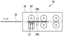
図12は、本実施形態に係る磁気センサを自動預け払い機(ATM機)へ搭載して紙幣識別装置を実現した場合の構成例を示す図である。図12の紙幣識別装置60は、紙幣30の搬送メカ26が組み込まれており、ローラー29等で規制される搬送面に図10に示される本実施形態の磁気センサ27と、光学ラインセンサ28a,28bとが配置されている。紙幣識別装置60は、そのセンサ出力を照合して、紙幣30の真贋判定や金種判別を行う。
FIG. 12 is a diagram illustrating a configuration example when the banknote identification device is realized by mounting the magnetic sensor according to the present embodiment on an automatic teller machine (ATM machine). The
さらに、図13は、本実施形態に係る磁気センサの他の利用例を示す図である。図13に示されるように、本実施形態の磁気センサ27の検知面6側にパーマロイや磁性トナー等の磁性体32を取り付けたアーム31を用意し、X軸方向に移動させることで、エンコーダー的に位置の判別をすることも可能である。磁気センサ27の磁石と磁性体32は十分離して利用することが可能であり、非接触式の位置検知装置としても、利用価値が大きい。
Furthermore, FIG. 13 is a figure which shows the other usage example of the magnetic sensor which concerns on this embodiment. As shown in FIG. 13, an
(まとめ)
上述した本発明の実施形態によれば、磁石上に磁性体が掛かることによる磁場変化の検知と、磁石間に磁性体が掛かることによる磁場変化の検知とを行うハイブリッドな構成となる。これにより、磁性体の磁場変化を最大限に引き出すことが可能となり、従来に比べ大幅なS/Nの改善が可能となる。また、これらの二つの磁気検知が補間関係にあることで、全体として不感帯を実質的に無くすことができ、磁性体が微小なものであっても取りこぼしがない検知、すなわち、高精度な検知が可能となる。
(Summary)
According to the above-described embodiment of the present invention, a hybrid configuration is employed in which a magnetic field change is detected when a magnetic material is applied to a magnet, and a magnetic field change is detected when a magnetic material is applied between the magnets. As a result, the magnetic field change of the magnetic material can be maximized, and the S / N can be greatly improved as compared with the conventional case. In addition, since these two magnetic detections are in an interpolating relationship, the dead zone as a whole can be substantially eliminated, and even if the magnetic material is minute, detection that is not missed, that is, highly accurate detection is possible. It becomes possible.
また、上記実施形態に係る磁気センサは、磁石のNSの中点を含みNS方向を法線とする平面内に磁気検出素子の検知面が位置するように構成されることで、磁気飽和しやすい高感度の磁気センサが利用可能となった。また、互いに隣接する磁気検出素子は、相対的に磁石の磁界変化が逆相となるため、差動動作にも適している。 In addition, the magnetic sensor according to the above-described embodiment is likely to be magnetically saturated by being configured such that the detection surface of the magnetic detection element is located in a plane including the midpoint of the NS of the magnet and having the NS direction as a normal line. A highly sensitive magnetic sensor has become available. In addition, the magnetic detection elements adjacent to each other are also suitable for differential operation because the magnetic field change of the magnet is relatively out of phase.
なお、上記実施形態では、磁気検出素子の配置を磁石のNS方向を法線とし磁石のNSの中点を含む平面上に配置したが、本発明はこれに限定されない。例えば、磁気検出素子(感磁素子)として、磁界検知レンジがゼロ磁界近傍だけでなく、広いレンジを持つ素子を用意する場合である。この場合、磁石のNS方向を法線とした場合、磁石のNSの中点を含む平面上を除いて、隣り合う各磁石のそれぞれの磁場変化と、隣り合う磁石間の磁場変化とを受けることが可能な任意の位置に適宜配置することで、高感度な磁界検出が可能となる。 In the above embodiment, the magnetic detection elements are arranged on a plane including the NS direction of the magnet as a normal line and the midpoint of the magnet NS, but the present invention is not limited to this. For example, as a magnetic detection element (magnetic sensing element), an element having a wide range in addition to the vicinity of the zero magnetic field in the magnetic field detection range is prepared. In this case, when the NS direction of the magnet is normal, except for the plane including the midpoint of the NS of the magnet, the magnetic field change of each adjacent magnet and the magnetic field change between adjacent magnets are received. Therefore, it is possible to detect a magnetic field with high sensitivity.
さらに、上記実施形態に係る磁気センサは、磁石の配列が媒体搬送面から見て、交互にS極、N極となるように配列されているため、マルチチャンネルのセンサへの適用が容易であり、磁気検知のラインセンサとして用いることができる。 Furthermore, the magnetic sensor according to the above-described embodiment is easily applied to a multi-channel sensor because the arrangement of magnets is alternately arranged to be S and N poles when viewed from the medium conveyance surface. It can be used as a line sensor for magnetic detection.
ここまで、本発明の実施形態について説明したが、本発明は上述した実施形態に限定されず、その技術的思想の範囲内において種々異なる形態にて実施されてよいことは言うまでもない。 The embodiments of the present invention have been described so far, but the present invention is not limited to the above-described embodiments, and it goes without saying that the present invention may be implemented in various forms within the scope of the technical idea.
なお、本発明の範囲は、図示され記載された例示的な実施形態に限定されるものではなく、本発明が目的とするものと均等な効果をもたらすすべての実施形態をも含む。さらに、本発明の範囲は、各請求項により画される発明の特徴の組み合わせに限定されるものではなく、すべての開示されたそれぞれの特徴のうち特定の特徴のあらゆる所望する組み合わせによって画されうる。 It should be noted that the scope of the present invention is not limited to the illustrated and described exemplary embodiments, but includes all embodiments that provide the same effects as those intended by the present invention. Further, the scope of the invention is not limited to the combinations of features of the invention defined by the claims, but may be defined by any desired combination of particular features among all the disclosed features. .
1 磁気媒体
2 磁気印刷部
4 磁石3a等のNS極の概ね中点を通り、NS方向を法線とする平面
3a、3b、3c 磁石
5a、5b 磁気検出素子
6a、6b 検知面
7 磁性薄膜
8 平面コイル
9 電極
10 磁気センサ
20 磁気センサ
21 発振回路
22 検波回路
23 増幅回路
24 マルチプレクサ
25 マイコン(CPU)
50、51 磁界
DESCRIPTION OF
50, 51 magnetic field
Claims (6)
隣り合う磁石の間には、隣り合う各磁石でそれぞれ形成される磁場変化と、隣り合う磁石間で形成される磁場変化とをそれぞれ受ける感磁素子が配置されたことを特徴とする磁界検出装置。 A magnetic field detection device that detects a change in the magnetic field of a plurality of magnets arranged by alternately moving a magnetic medium including a magnetic body and reversing a magnetic pole in a direction orthogonal to the moving direction ,
A magnetic field detecting device is provided between adjacent magnets, each of which is provided with a magnetosensitive element that receives a magnetic field change formed by each adjacent magnet and a magnetic field change formed between adjacent magnets. .
複数の磁石と複数の感磁素子とが略直線上に交互に配置されて構成され、
前記複数の磁石は、そのNS方向が前記磁気媒体を移動する面に対して概ね垂直となるように、かつ前記磁気媒体の移動方向と垂直な方向へ略等間隔に配置されるとともに、前記複数の磁石は、前記磁気媒体に接する側の磁極が交互に入れ替わるように配列され、
前記複数の感磁素子は、前記略直線方向に磁界検知方向を有するように配置され、
前記複数の感磁素子のそれぞれは、前記磁性体が自素子に隣接する2つの磁石のそれぞれの磁極上に近接することで発生する前記2つの磁石それぞれの磁場変化と、前記2つの磁石の磁極間に前記磁性体が近接することで発生する前記磁性体の磁化による前記2つの磁石間の磁場変化と、を同時に検出することを特徴とする磁界検出装置。 Magnetic media containing the magnetic substance is moved, a magnetic field detecting apparatus for detecting a change in the magnetic field of a plurality of magnets arranged side by side alternately with poles reversed in a direction perpendicular to the moving direction of said magnetic medium,
A plurality of magnets and a plurality of magnetosensitive elements are alternately arranged on a substantially straight line,
The plurality of magnets are arranged substantially equidistantly in a direction perpendicular to the moving direction of the magnetic medium such that the NS direction thereof is substantially perpendicular to a surface moving the magnetic medium. The magnets are arranged so that the magnetic poles in contact with the magnetic medium are alternately switched,
The plurality of magnetosensitive elements are arranged to have a magnetic field detection direction in the substantially linear direction ,
Each of the plurality of magnetosensitive elements includes a magnetic field change of each of the two magnets generated when the magnetic body is close to the magnetic poles of the two magnets adjacent to the element, and the magnetic poles of the two magnets. A magnetic field detecting device for simultaneously detecting a change in magnetic field between the two magnets due to magnetization of the magnetic material, which is generated when the magnetic material is in proximity.
高周波電流を前記感磁素子の磁界検知部である磁性薄膜に印加する電流印加部と、
前記感磁素子の前記磁性薄膜に積層されたコイルから検波回路により前記感磁素子のセンサ電圧を取り出すセンサ電圧取得部と、
前記センサ電圧を増幅する増幅回路と、
前記複数のチャンネルを切り替えるマルチプレクサと、
前記マルチプレクサからの出力を数値化して演算処理を行う演算部と、
を有する磁気識別装置。 A magnetic identification device having a plurality of channels constituted by the magnetic field detection device according to any one of claims 1 to 5,
A current applying unit that applies a high-frequency current to a magnetic thin film that is a magnetic field detecting unit of the magnetosensitive element;
A sensor voltage acquisition unit for extracting a sensor voltage of the magnetosensitive element by a detection circuit from a coil laminated on the magnetic thin film of the magnetosensitive element;
An amplifier circuit for amplifying the sensor voltage;
A multiplexer for switching the plurality of channels;
An arithmetic unit that performs arithmetic processing by digitizing the output from the multiplexer;
A magnetic identification device.
Priority Applications (2)
| Application Number | Priority Date | Filing Date | Title |
|---|---|---|---|
| JP2014078054A JP6359858B2 (en) | 2014-04-04 | 2014-04-04 | Magnetic field detection device and magnetic identification device |
| CN201510157710.XA CN104977547B (en) | 2014-04-04 | 2015-04-03 | Detector for magnetic field and magnetic identification device |
Applications Claiming Priority (1)
| Application Number | Priority Date | Filing Date | Title |
|---|---|---|---|
| JP2014078054A JP6359858B2 (en) | 2014-04-04 | 2014-04-04 | Magnetic field detection device and magnetic identification device |
Publications (3)
| Publication Number | Publication Date |
|---|---|
| JP2015200523A JP2015200523A (en) | 2015-11-12 |
| JP2015200523A5 JP2015200523A5 (en) | 2017-03-16 |
| JP6359858B2 true JP6359858B2 (en) | 2018-07-18 |
Family
ID=54274232
Family Applications (1)
| Application Number | Title | Priority Date | Filing Date |
|---|---|---|---|
| JP2014078054A Active JP6359858B2 (en) | 2014-04-04 | 2014-04-04 | Magnetic field detection device and magnetic identification device |
Country Status (2)
| Country | Link |
|---|---|
| JP (1) | JP6359858B2 (en) |
| CN (1) | CN104977547B (en) |
Families Citing this family (7)
| Publication number | Priority date | Publication date | Assignee | Title |
|---|---|---|---|---|
| CN105093135A (en) * | 2015-06-25 | 2015-11-25 | 无锡乐尔科技有限公司 | Evaluation method for magnetic head and magnetic medium |
| JP6974897B2 (en) * | 2016-04-19 | 2021-12-01 | キヤノン電子株式会社 | Magnetic identification device |
| JP6789711B2 (en) * | 2016-07-29 | 2020-11-25 | キヤノン電子株式会社 | Magnetic identification device |
| CN106353701A (en) * | 2016-08-24 | 2017-01-25 | 明光万佳联众电子有限公司 | Automatic-measurement constant magnetic field separator |
| WO2019151422A1 (en) * | 2018-01-31 | 2019-08-08 | キヤノン電子株式会社 | Inspection device |
| JP7059080B2 (en) * | 2018-04-09 | 2022-04-25 | キヤノン電子株式会社 | Magnetic identification device |
| CN111896900B (en) * | 2020-07-06 | 2021-05-25 | 苏州佳祺仕信息科技有限公司 | Multi-probe Gaussian detection device |
Family Cites Families (13)
| Publication number | Priority date | Publication date | Assignee | Title |
|---|---|---|---|---|
| JPH0725728Y2 (en) * | 1988-05-27 | 1995-06-07 | 株式会社村田製作所 | Magnetoresistive element array |
| JP3226071B2 (en) * | 1993-12-28 | 2001-11-05 | 東京瓦斯株式会社 | Magnetic flaw detection |
| JP3064293B2 (en) * | 1997-02-18 | 2000-07-12 | トヨタ自動車株式会社 | Rotation sensor |
| JP2002246568A (en) * | 2001-02-16 | 2002-08-30 | Sony Corp | Magnetic memory device and its manufacturing method |
| JP4160330B2 (en) * | 2002-07-12 | 2008-10-01 | キヤノン電子株式会社 | Magnetic field detection circuit |
| KR100801853B1 (en) * | 2004-02-27 | 2008-02-11 | 가부시키가이샤 무라타 세이사쿠쇼 | Prolonged magnetic sensor |
| WO2006039439A2 (en) * | 2004-09-30 | 2006-04-13 | Cummins-Allison Corp. | Magnetic detection system for use in currency processing and method and apparatus for using the same |
| JP4940565B2 (en) * | 2005-03-28 | 2012-05-30 | ヤマハ株式会社 | Manufacturing method of magnetic sensor |
| JP4837749B2 (en) * | 2006-12-13 | 2011-12-14 | アルプス電気株式会社 | Magnetic sensor and magnetic encoder using the same |
| JP5362188B2 (en) * | 2007-03-29 | 2013-12-11 | キヤノン電子株式会社 | Magnetic detection sensor |
| JP5227527B2 (en) * | 2007-03-29 | 2013-07-03 | キヤノン電子株式会社 | Magnetic detection sensor |
| JP5494591B2 (en) * | 2010-09-28 | 2014-05-14 | 株式会社村田製作所 | Long magnetic sensor |
| JP5603259B2 (en) * | 2011-01-14 | 2014-10-08 | 日立オムロンターミナルソリューションズ株式会社 | Paper sheet identification device |
-
2014
- 2014-04-04 JP JP2014078054A patent/JP6359858B2/en active Active
-
2015
- 2015-04-03 CN CN201510157710.XA patent/CN104977547B/en active Active
Also Published As
| Publication number | Publication date |
|---|---|
| CN104977547A (en) | 2015-10-14 |
| JP2015200523A (en) | 2015-11-12 |
| CN104977547B (en) | 2018-04-20 |
Similar Documents
| Publication | Publication Date | Title |
|---|---|---|
| JP6359858B2 (en) | Magnetic field detection device and magnetic identification device | |
| JP5867235B2 (en) | Magnetic sensor device | |
| CN101273247B (en) | Magnetic sensor and magnetic sensing method | |
| US9279866B2 (en) | Magnetic sensor | |
| JP5719515B2 (en) | Magnetic sensor device | |
| EP3026451B1 (en) | Single magnetoresistor tmr magnetic field sensor chip and magnetic currency detector head | |
| KR20140051385A (en) | Measuring device for measuring the magnetic properties of the surroundings of the measuring device | |
| JP5227527B2 (en) | Magnetic detection sensor | |
| JP5799882B2 (en) | Magnetic sensor device | |
| WO2018139233A1 (en) | Magnetoresistive effect element unit and magnetoresistive effect element device | |
| JP6550587B2 (en) | Magnetic line sensor and discrimination device using the same | |
| EP3133561B1 (en) | An in-plane magnetic image sensor chip | |
| JP2008046104A (en) | Manufacturing method of magnetic encoder and magnetic scale | |
| CN113302693B (en) | Magnetic identification sensor | |
| JP5243725B2 (en) | Magnetic detection sensor | |
| JP5861551B2 (en) | Magnetic sensor device | |
| JP6315802B2 (en) | Magnetic sensor device | |
| JP6980166B1 (en) | Magnetic sensor device | |
| JP2022189283A (en) | Magnetic identification sensor and magnetic identification device | |
| WO2023127576A1 (en) | Magnetic feature detecting device, and paper sheet identifying device | |
| JP6974897B2 (en) | Magnetic identification device | |
| JP2019184382A (en) | Magnetic identifying device |
Legal Events
| Date | Code | Title | Description |
|---|---|---|---|
| A521 | Request for written amendment filed |
Free format text: JAPANESE INTERMEDIATE CODE: A523 Effective date: 20170208 |
|
| A621 | Written request for application examination |
Free format text: JAPANESE INTERMEDIATE CODE: A621 Effective date: 20170208 |
|
| A977 | Report on retrieval |
Free format text: JAPANESE INTERMEDIATE CODE: A971007 Effective date: 20171116 |
|
| A131 | Notification of reasons for refusal |
Free format text: JAPANESE INTERMEDIATE CODE: A131 Effective date: 20171128 |
|
| A521 | Request for written amendment filed |
Free format text: JAPANESE INTERMEDIATE CODE: A523 Effective date: 20180129 |
|
| TRDD | Decision of grant or rejection written | ||
| A01 | Written decision to grant a patent or to grant a registration (utility model) |
Free format text: JAPANESE INTERMEDIATE CODE: A01 Effective date: 20180605 |
|
| A61 | First payment of annual fees (during grant procedure) |
Free format text: JAPANESE INTERMEDIATE CODE: A61 Effective date: 20180621 |
|
| R150 | Certificate of patent or registration of utility model |
Ref document number: 6359858 Country of ref document: JP Free format text: JAPANESE INTERMEDIATE CODE: R150 |
|
| R250 | Receipt of annual fees |
Free format text: JAPANESE INTERMEDIATE CODE: R250 |
|
| R250 | Receipt of annual fees |
Free format text: JAPANESE INTERMEDIATE CODE: R250 |
|
| R250 | Receipt of annual fees |
Free format text: JAPANESE INTERMEDIATE CODE: R250 |