JP6310560B2 - Laser printing system - Google Patents
Laser printing system Download PDFInfo
- Publication number
- JP6310560B2 JP6310560B2 JP2016538064A JP2016538064A JP6310560B2 JP 6310560 B2 JP6310560 B2 JP 6310560B2 JP 2016538064 A JP2016538064 A JP 2016538064A JP 2016538064 A JP2016538064 A JP 2016538064A JP 6310560 B2 JP6310560 B2 JP 6310560B2
- Authority
- JP
- Japan
- Prior art keywords
- laser
- array
- printing system
- module
- use surface
- Prior art date
- Legal status (The legal status is an assumption and is not a legal conclusion. Google has not performed a legal analysis and makes no representation as to the accuracy of the status listed.)
- Active
Links
- 238000007648 laser printing Methods 0.000 title claims description 73
- 239000004065 semiconductor Substances 0.000 claims description 74
- 230000003287 optical effect Effects 0.000 claims description 55
- 238000003491 array Methods 0.000 claims description 40
- 238000000034 method Methods 0.000 claims description 18
- 238000005286 illumination Methods 0.000 claims description 11
- 238000003384 imaging method Methods 0.000 claims description 10
- 230000001678 irradiating effect Effects 0.000 claims description 2
- 238000009826 distribution Methods 0.000 description 8
- 238000010586 diagram Methods 0.000 description 7
- 238000007639 printing Methods 0.000 description 7
- 238000010146 3D printing Methods 0.000 description 5
- 230000001419 dependent effect Effects 0.000 description 5
- 239000000463 material Substances 0.000 description 5
- 238000010438 heat treatment Methods 0.000 description 4
- 238000012545 processing Methods 0.000 description 3
- 230000008901 benefit Effects 0.000 description 2
- 230000007547 defect Effects 0.000 description 2
- 238000013461 design Methods 0.000 description 2
- 239000011521 glass Substances 0.000 description 2
- 238000004519 manufacturing process Methods 0.000 description 2
- 238000002844 melting Methods 0.000 description 2
- 230000008018 melting Effects 0.000 description 2
- 230000004048 modification Effects 0.000 description 2
- 238000012986 modification Methods 0.000 description 2
- 230000009467 reduction Effects 0.000 description 2
- 238000010521 absorption reaction Methods 0.000 description 1
- 230000001154 acute effect Effects 0.000 description 1
- 230000006978 adaptation Effects 0.000 description 1
- 239000000654 additive Substances 0.000 description 1
- 230000000996 additive effect Effects 0.000 description 1
- 238000013459 approach Methods 0.000 description 1
- 238000004587 chromatography analysis Methods 0.000 description 1
- 230000010485 coping Effects 0.000 description 1
- 229910003460 diamond Inorganic materials 0.000 description 1
- 239000010432 diamond Substances 0.000 description 1
- 238000009792 diffusion process Methods 0.000 description 1
- 238000000465 moulding Methods 0.000 description 1
- 239000000843 powder Substances 0.000 description 1
- 230000008569 process Effects 0.000 description 1
- 230000005855 radiation Effects 0.000 description 1
- 238000005245 sintering Methods 0.000 description 1
- 230000007704 transition Effects 0.000 description 1
Images


Classifications
-
- B—PERFORMING OPERATIONS; TRANSPORTING
- B41—PRINTING; LINING MACHINES; TYPEWRITERS; STAMPS
- B41J—TYPEWRITERS; SELECTIVE PRINTING MECHANISMS, i.e. MECHANISMS PRINTING OTHERWISE THAN FROM A FORME; CORRECTION OF TYPOGRAPHICAL ERRORS
- B41J2/00—Typewriters or selective printing mechanisms characterised by the printing or marking process for which they are designed
- B41J2/435—Typewriters or selective printing mechanisms characterised by the printing or marking process for which they are designed characterised by selective application of radiation to a printing material or impression-transfer material
- B41J2/447—Typewriters or selective printing mechanisms characterised by the printing or marking process for which they are designed characterised by selective application of radiation to a printing material or impression-transfer material using arrays of radiation sources
- B41J2/45—Typewriters or selective printing mechanisms characterised by the printing or marking process for which they are designed characterised by selective application of radiation to a printing material or impression-transfer material using arrays of radiation sources using light-emitting diode [LED] or laser arrays
-
- B—PERFORMING OPERATIONS; TRANSPORTING
- B29—WORKING OF PLASTICS; WORKING OF SUBSTANCES IN A PLASTIC STATE IN GENERAL
- B29C—SHAPING OR JOINING OF PLASTICS; SHAPING OF MATERIAL IN A PLASTIC STATE, NOT OTHERWISE PROVIDED FOR; AFTER-TREATMENT OF THE SHAPED PRODUCTS, e.g. REPAIRING
- B29C64/00—Additive manufacturing, i.e. manufacturing of three-dimensional [3D] objects by additive deposition, additive agglomeration or additive layering, e.g. by 3D printing, stereolithography or selective laser sintering
- B29C64/10—Processes of additive manufacturing
- B29C64/141—Processes of additive manufacturing using only solid materials
- B29C64/153—Processes of additive manufacturing using only solid materials using layers of powder being selectively joined, e.g. by selective laser sintering or melting
-
- B—PERFORMING OPERATIONS; TRANSPORTING
- B22—CASTING; POWDER METALLURGY
- B22F—WORKING METALLIC POWDER; MANUFACTURE OF ARTICLES FROM METALLIC POWDER; MAKING METALLIC POWDER; APPARATUS OR DEVICES SPECIALLY ADAPTED FOR METALLIC POWDER
- B22F12/00—Apparatus or devices specially adapted for additive manufacturing; Auxiliary means for additive manufacturing; Combinations of additive manufacturing apparatus or devices with other processing apparatus or devices
- B22F12/38—Housings, e.g. machine housings
-
- B—PERFORMING OPERATIONS; TRANSPORTING
- B22—CASTING; POWDER METALLURGY
- B22F—WORKING METALLIC POWDER; MANUFACTURE OF ARTICLES FROM METALLIC POWDER; MAKING METALLIC POWDER; APPARATUS OR DEVICES SPECIALLY ADAPTED FOR METALLIC POWDER
- B22F12/00—Apparatus or devices specially adapted for additive manufacturing; Auxiliary means for additive manufacturing; Combinations of additive manufacturing apparatus or devices with other processing apparatus or devices
- B22F12/40—Radiation means
- B22F12/41—Radiation means characterised by the type, e.g. laser or electron beam
- B22F12/42—Light-emitting diodes [LED]
-
- B—PERFORMING OPERATIONS; TRANSPORTING
- B22—CASTING; POWDER METALLURGY
- B22F—WORKING METALLIC POWDER; MANUFACTURE OF ARTICLES FROM METALLIC POWDER; MAKING METALLIC POWDER; APPARATUS OR DEVICES SPECIALLY ADAPTED FOR METALLIC POWDER
- B22F12/00—Apparatus or devices specially adapted for additive manufacturing; Auxiliary means for additive manufacturing; Combinations of additive manufacturing apparatus or devices with other processing apparatus or devices
- B22F12/40—Radiation means
- B22F12/44—Radiation means characterised by the configuration of the radiation means
- B22F12/45—Two or more
-
- B—PERFORMING OPERATIONS; TRANSPORTING
- B22—CASTING; POWDER METALLURGY
- B22F—WORKING METALLIC POWDER; MANUFACTURE OF ARTICLES FROM METALLIC POWDER; MAKING METALLIC POWDER; APPARATUS OR DEVICES SPECIALLY ADAPTED FOR METALLIC POWDER
- B22F12/00—Apparatus or devices specially adapted for additive manufacturing; Auxiliary means for additive manufacturing; Combinations of additive manufacturing apparatus or devices with other processing apparatus or devices
- B22F12/40—Radiation means
- B22F12/46—Radiation means with translatory movement
- B22F12/47—Radiation means with translatory movement parallel to the deposition plane
-
- B—PERFORMING OPERATIONS; TRANSPORTING
- B22—CASTING; POWDER METALLURGY
- B22F—WORKING METALLIC POWDER; MANUFACTURE OF ARTICLES FROM METALLIC POWDER; MAKING METALLIC POWDER; APPARATUS OR DEVICES SPECIALLY ADAPTED FOR METALLIC POWDER
- B22F12/00—Apparatus or devices specially adapted for additive manufacturing; Auxiliary means for additive manufacturing; Combinations of additive manufacturing apparatus or devices with other processing apparatus or devices
- B22F12/40—Radiation means
- B22F12/49—Scanners
-
- B—PERFORMING OPERATIONS; TRANSPORTING
- B23—MACHINE TOOLS; METAL-WORKING NOT OTHERWISE PROVIDED FOR
- B23K—SOLDERING OR UNSOLDERING; WELDING; CLADDING OR PLATING BY SOLDERING OR WELDING; CUTTING BY APPLYING HEAT LOCALLY, e.g. FLAME CUTTING; WORKING BY LASER BEAM
- B23K26/00—Working by laser beam, e.g. welding, cutting or boring
- B23K26/02—Positioning or observing the workpiece, e.g. with respect to the point of impact; Aligning, aiming or focusing the laser beam
- B23K26/06—Shaping the laser beam, e.g. by masks or multi-focusing
- B23K26/064—Shaping the laser beam, e.g. by masks or multi-focusing by means of optical elements, e.g. lenses, mirrors or prisms
-
- B—PERFORMING OPERATIONS; TRANSPORTING
- B23—MACHINE TOOLS; METAL-WORKING NOT OTHERWISE PROVIDED FOR
- B23K—SOLDERING OR UNSOLDERING; WELDING; CLADDING OR PLATING BY SOLDERING OR WELDING; CUTTING BY APPLYING HEAT LOCALLY, e.g. FLAME CUTTING; WORKING BY LASER BEAM
- B23K26/00—Working by laser beam, e.g. welding, cutting or boring
- B23K26/08—Devices involving relative movement between laser beam and workpiece
- B23K26/083—Devices involving movement of the workpiece in at least one axial direction
- B23K26/0853—Devices involving movement of the workpiece in at least in two axial directions, e.g. in a plane
-
- B—PERFORMING OPERATIONS; TRANSPORTING
- B23—MACHINE TOOLS; METAL-WORKING NOT OTHERWISE PROVIDED FOR
- B23K—SOLDERING OR UNSOLDERING; WELDING; CLADDING OR PLATING BY SOLDERING OR WELDING; CUTTING BY APPLYING HEAT LOCALLY, e.g. FLAME CUTTING; WORKING BY LASER BEAM
- B23K26/00—Working by laser beam, e.g. welding, cutting or boring
- B23K26/34—Laser welding for purposes other than joining
- B23K26/342—Build-up welding
-
- B—PERFORMING OPERATIONS; TRANSPORTING
- B29—WORKING OF PLASTICS; WORKING OF SUBSTANCES IN A PLASTIC STATE IN GENERAL
- B29C—SHAPING OR JOINING OF PLASTICS; SHAPING OF MATERIAL IN A PLASTIC STATE, NOT OTHERWISE PROVIDED FOR; AFTER-TREATMENT OF THE SHAPED PRODUCTS, e.g. REPAIRING
- B29C64/00—Additive manufacturing, i.e. manufacturing of three-dimensional [3D] objects by additive deposition, additive agglomeration or additive layering, e.g. by 3D printing, stereolithography or selective laser sintering
- B29C64/20—Apparatus for additive manufacturing; Details thereof or accessories therefor
- B29C64/25—Housings, e.g. machine housings
-
- B—PERFORMING OPERATIONS; TRANSPORTING
- B29—WORKING OF PLASTICS; WORKING OF SUBSTANCES IN A PLASTIC STATE IN GENERAL
- B29C—SHAPING OR JOINING OF PLASTICS; SHAPING OF MATERIAL IN A PLASTIC STATE, NOT OTHERWISE PROVIDED FOR; AFTER-TREATMENT OF THE SHAPED PRODUCTS, e.g. REPAIRING
- B29C64/00—Additive manufacturing, i.e. manufacturing of three-dimensional [3D] objects by additive deposition, additive agglomeration or additive layering, e.g. by 3D printing, stereolithography or selective laser sintering
- B29C64/20—Apparatus for additive manufacturing; Details thereof or accessories therefor
- B29C64/264—Arrangements for irradiation
- B29C64/268—Arrangements for irradiation using laser beams; using electron beams [EB]
-
- B—PERFORMING OPERATIONS; TRANSPORTING
- B29—WORKING OF PLASTICS; WORKING OF SUBSTANCES IN A PLASTIC STATE IN GENERAL
- B29C—SHAPING OR JOINING OF PLASTICS; SHAPING OF MATERIAL IN A PLASTIC STATE, NOT OTHERWISE PROVIDED FOR; AFTER-TREATMENT OF THE SHAPED PRODUCTS, e.g. REPAIRING
- B29C64/00—Additive manufacturing, i.e. manufacturing of three-dimensional [3D] objects by additive deposition, additive agglomeration or additive layering, e.g. by 3D printing, stereolithography or selective laser sintering
- B29C64/20—Apparatus for additive manufacturing; Details thereof or accessories therefor
- B29C64/264—Arrangements for irradiation
- B29C64/277—Arrangements for irradiation using multiple radiation means, e.g. micromirrors or multiple light-emitting diodes [LED]
- B29C64/282—Arrangements for irradiation using multiple radiation means, e.g. micromirrors or multiple light-emitting diodes [LED] of the same type, e.g. using different energy levels
-
- B—PERFORMING OPERATIONS; TRANSPORTING
- B29—WORKING OF PLASTICS; WORKING OF SUBSTANCES IN A PLASTIC STATE IN GENERAL
- B29C—SHAPING OR JOINING OF PLASTICS; SHAPING OF MATERIAL IN A PLASTIC STATE, NOT OTHERWISE PROVIDED FOR; AFTER-TREATMENT OF THE SHAPED PRODUCTS, e.g. REPAIRING
- B29C64/00—Additive manufacturing, i.e. manufacturing of three-dimensional [3D] objects by additive deposition, additive agglomeration or additive layering, e.g. by 3D printing, stereolithography or selective laser sintering
- B29C64/30—Auxiliary operations or equipment
- B29C64/386—Data acquisition or data processing for additive manufacturing
- B29C64/393—Data acquisition or data processing for additive manufacturing for controlling or regulating additive manufacturing processes
-
- B—PERFORMING OPERATIONS; TRANSPORTING
- B33—ADDITIVE MANUFACTURING TECHNOLOGY
- B33Y—ADDITIVE MANUFACTURING, i.e. MANUFACTURING OF THREE-DIMENSIONAL [3-D] OBJECTS BY ADDITIVE DEPOSITION, ADDITIVE AGGLOMERATION OR ADDITIVE LAYERING, e.g. BY 3-D PRINTING, STEREOLITHOGRAPHY OR SELECTIVE LASER SINTERING
- B33Y10/00—Processes of additive manufacturing
-
- B—PERFORMING OPERATIONS; TRANSPORTING
- B33—ADDITIVE MANUFACTURING TECHNOLOGY
- B33Y—ADDITIVE MANUFACTURING, i.e. MANUFACTURING OF THREE-DIMENSIONAL [3-D] OBJECTS BY ADDITIVE DEPOSITION, ADDITIVE AGGLOMERATION OR ADDITIVE LAYERING, e.g. BY 3-D PRINTING, STEREOLITHOGRAPHY OR SELECTIVE LASER SINTERING
- B33Y30/00—Apparatus for additive manufacturing; Details thereof or accessories therefor
-
- B—PERFORMING OPERATIONS; TRANSPORTING
- B33—ADDITIVE MANUFACTURING TECHNOLOGY
- B33Y—ADDITIVE MANUFACTURING, i.e. MANUFACTURING OF THREE-DIMENSIONAL [3-D] OBJECTS BY ADDITIVE DEPOSITION, ADDITIVE AGGLOMERATION OR ADDITIVE LAYERING, e.g. BY 3-D PRINTING, STEREOLITHOGRAPHY OR SELECTIVE LASER SINTERING
- B33Y50/00—Data acquisition or data processing for additive manufacturing
- B33Y50/02—Data acquisition or data processing for additive manufacturing for controlling or regulating additive manufacturing processes
-
- B—PERFORMING OPERATIONS; TRANSPORTING
- B41—PRINTING; LINING MACHINES; TYPEWRITERS; STAMPS
- B41J—TYPEWRITERS; SELECTIVE PRINTING MECHANISMS, i.e. MECHANISMS PRINTING OTHERWISE THAN FROM A FORME; CORRECTION OF TYPOGRAPHICAL ERRORS
- B41J2/00—Typewriters or selective printing mechanisms characterised by the printing or marking process for which they are designed
- B41J2/435—Typewriters or selective printing mechanisms characterised by the printing or marking process for which they are designed characterised by selective application of radiation to a printing material or impression-transfer material
- B41J2/447—Typewriters or selective printing mechanisms characterised by the printing or marking process for which they are designed characterised by selective application of radiation to a printing material or impression-transfer material using arrays of radiation sources
- B41J2/45—Typewriters or selective printing mechanisms characterised by the printing or marking process for which they are designed characterised by selective application of radiation to a printing material or impression-transfer material using arrays of radiation sources using light-emitting diode [LED] or laser arrays
- B41J2/451—Special optical means therefor, e.g. lenses, mirrors, focusing means
-
- B—PERFORMING OPERATIONS; TRANSPORTING
- B41—PRINTING; LINING MACHINES; TYPEWRITERS; STAMPS
- B41J—TYPEWRITERS; SELECTIVE PRINTING MECHANISMS, i.e. MECHANISMS PRINTING OTHERWISE THAN FROM A FORME; CORRECTION OF TYPOGRAPHICAL ERRORS
- B41J2/00—Typewriters or selective printing mechanisms characterised by the printing or marking process for which they are designed
- B41J2/435—Typewriters or selective printing mechanisms characterised by the printing or marking process for which they are designed characterised by selective application of radiation to a printing material or impression-transfer material
- B41J2/447—Typewriters or selective printing mechanisms characterised by the printing or marking process for which they are designed characterised by selective application of radiation to a printing material or impression-transfer material using arrays of radiation sources
- B41J2/455—Typewriters or selective printing mechanisms characterised by the printing or marking process for which they are designed characterised by selective application of radiation to a printing material or impression-transfer material using arrays of radiation sources using laser arrays, the laser array being smaller than the medium to be recorded
-
- G—PHYSICS
- G02—OPTICS
- G02B—OPTICAL ELEMENTS, SYSTEMS OR APPARATUS
- G02B3/00—Simple or compound lenses
- G02B3/0006—Arrays
-
- H—ELECTRICITY
- H01—ELECTRIC ELEMENTS
- H01S—DEVICES USING THE PROCESS OF LIGHT AMPLIFICATION BY STIMULATED EMISSION OF RADIATION [LASER] TO AMPLIFY OR GENERATE LIGHT; DEVICES USING STIMULATED EMISSION OF ELECTROMAGNETIC RADIATION IN WAVE RANGES OTHER THAN OPTICAL
- H01S5/00—Semiconductor lasers
- H01S5/005—Optical components external to the laser cavity, specially adapted therefor, e.g. for homogenisation or merging of the beams or for manipulating laser pulses, e.g. pulse shaping
- H01S5/0071—Optical components external to the laser cavity, specially adapted therefor, e.g. for homogenisation or merging of the beams or for manipulating laser pulses, e.g. pulse shaping for beam steering, e.g. using a mirror outside the cavity to change the beam direction
-
- H—ELECTRICITY
- H01—ELECTRIC ELEMENTS
- H01S—DEVICES USING THE PROCESS OF LIGHT AMPLIFICATION BY STIMULATED EMISSION OF RADIATION [LASER] TO AMPLIFY OR GENERATE LIGHT; DEVICES USING STIMULATED EMISSION OF ELECTROMAGNETIC RADIATION IN WAVE RANGES OTHER THAN OPTICAL
- H01S5/00—Semiconductor lasers
- H01S5/40—Arrangement of two or more semiconductor lasers, not provided for in groups H01S5/02 - H01S5/30
- H01S5/42—Arrays of surface emitting lasers
- H01S5/423—Arrays of surface emitting lasers having a vertical cavity
-
- B—PERFORMING OPERATIONS; TRANSPORTING
- B22—CASTING; POWDER METALLURGY
- B22F—WORKING METALLIC POWDER; MANUFACTURE OF ARTICLES FROM METALLIC POWDER; MAKING METALLIC POWDER; APPARATUS OR DEVICES SPECIALLY ADAPTED FOR METALLIC POWDER
- B22F10/00—Additive manufacturing of workpieces or articles from metallic powder
- B22F10/20—Direct sintering or melting
- B22F10/28—Powder bed fusion, e.g. selective laser melting [SLM] or electron beam melting [EBM]
-
- G—PHYSICS
- G03—PHOTOGRAPHY; CINEMATOGRAPHY; ANALOGOUS TECHNIQUES USING WAVES OTHER THAN OPTICAL WAVES; ELECTROGRAPHY; HOLOGRAPHY
- G03G—ELECTROGRAPHY; ELECTROPHOTOGRAPHY; MAGNETOGRAPHY
- G03G15/00—Apparatus for electrographic processes using a charge pattern
- G03G15/22—Apparatus for electrographic processes using a charge pattern involving the combination of more than one step according to groups G03G13/02 - G03G13/20
- G03G15/225—Apparatus for electrographic processes using a charge pattern involving the combination of more than one step according to groups G03G13/02 - G03G13/20 using contact-printing
Landscapes
- Engineering & Computer Science (AREA)
- Chemical & Material Sciences (AREA)
- Materials Engineering (AREA)
- Physics & Mathematics (AREA)
- Optics & Photonics (AREA)
- Manufacturing & Machinery (AREA)
- Health & Medical Sciences (AREA)
- Toxicology (AREA)
- General Health & Medical Sciences (AREA)
- Mechanical Engineering (AREA)
- Plasma & Fusion (AREA)
- General Physics & Mathematics (AREA)
- Microelectronics & Electronic Packaging (AREA)
- Condensed Matter Physics & Semiconductors (AREA)
- Electromagnetism (AREA)
- Semiconductor Lasers (AREA)
- Laser Beam Processing (AREA)
- Manufacture Or Reproduction Of Printing Formes (AREA)
- Printers Or Recording Devices Using Electromagnetic And Radiation Means (AREA)
- Powder Metallurgy (AREA)
- Laser Beam Printer (AREA)
Description
本発明は、レーザ印刷システム及びレーザ印刷の方法に関する。レーザ印刷は、例えば急速なプロトタイピングのために使用される積層造形のためのレーザによる3D印刷及び文書の印刷に言及する。 The present invention relates to a laser printing system and a laser printing method. Laser printing refers to laser 3D printing and document printing, for example, for additive manufacturing used for rapid prototyping.
従来のレーザプリンタ及び選択的レーザ溶融マシンは、照射されるべきエリアに渡ってレーザを走査するための単一の高出力レーザ及びスキャナからなる。処理速度を増大させるために、幾つかの独立したチャネル(即ち、エリアの重大な部分を覆うレーザのアドレス指定可能なアレイ)を伴う印刷ヘッドを有することが望ましい。好ましくは、印字ヘッドが一方向にのみ移動するのを必要とするように、印刷ヘッドは、画素毎に1つのアドレス指定可能なレーザソースによって印刷されるべきエリアの全幅を覆う。斯様なアドレス指定可能なアレイのサービスコスト及び信頼性が問題になり得る。 Conventional laser printers and selective laser melting machines consist of a single high power laser and scanner for scanning the laser across the area to be illuminated. In order to increase processing speed, it is desirable to have a printhead with several independent channels (ie, an addressable array of lasers covering a significant portion of the area). Preferably, the print head covers the entire width of the area to be printed by one addressable laser source per pixel so that the print head only needs to move in one direction. The service cost and reliability of such addressable arrays can be a problem.
米国特許出願公開第2005/0151828号明細書は、ゼログラフィのレーザ印刷のためのデバイスを開示している。ゼログラフィの印刷システムは、複数のマイクロ光学発光アレイを含むレーザプリントバー結像装置アセンブリを有する。マイクロ光学発光アレイは、複数の垂直キャビティ面発光レーザを含み、ここで、各垂直キャビティ面発光レーザは、マイクロ光学要素によって集光される。 US Patent Application Publication No. 2005/0151828 discloses a device for xerographic laser printing. The printing system of xerography has a laser print bar imaging assembly including a plurality of micro-optical emission array. The micro-optical emission array includes a plurality of vertical cavity surface emitting lasers, where each vertical cavity surface emitting laser is collected by a micro optical element.
それ故、本発明の目的は、改良されたレーザ印刷システム及びレーザ印刷の対応する方法を提供することにある。 The object of the present invention is therefore to provide an improved laser printing system and a corresponding method of laser printing.
第1の態様によれば、使用面においてレーザ印刷システムのレーザモジュールに対して移動するオブジェクトを照射するためのレーザ印刷システムが提供される。レーザモジュールは、半導体レーザの少なくとも2つのレーザアレイと、少なくとも1つの光学要素とを有する。光学要素は、1つのレーザアレイの半導体レーザのレーザ光がレーザ印刷システムの使用面における1つの画素に対して結像されるとともに画素のエリア要素が少なくとも2つの半導体レーザによって照射されるように、レーザアレイにより放射されたレーザ光を結像するように適合される。 According to a first aspect, there is provided a laser printing system for irradiating a moving object on a use surface with respect to a laser module of the laser printing system. The laser module has at least two laser arrays of semiconductor lasers and at least one optical element. The optical element is such that the laser light of the semiconductor laser of one laser array is imaged onto one pixel on the working surface of the laser printing system and the area element of the pixel is illuminated by at least two semiconductor lasers, It is adapted to image the laser light emitted by the laser array.
既知のレーザ印刷システムは、単一の高出力レーザ又はレーザのアレイのいずれかを用いる。高出力レーザの場合には、例えば、単一の端発光半導体レーザが用いられ得るのに対し、レーザアレイの場合には、垂直キャビティ面発光レーザ(VCSELs;Vertical Cavity Surface Emitting Lasers)が好ましくは用いられる。VCSELアレイは、ウェーハベースの処理において容易に製造され得るが、通常、端発光半導体レーザとしてより少ない出力を放射する。これらの既知のレーザ印刷システムの光学システムは、各半導体レーザの発光層を使用面に投射又は集光する。 Known laser printing systems use either a single high power laser or an array of lasers. In the case of a high power laser, for example, a single edge emitting semiconductor laser can be used, whereas in the case of a laser array, vertical cavity surface emitting lasers (VCSELs) are preferably used. It is done. VCSEL arrays can be easily manufactured in wafer-based processing, but typically emit less output as edge emitting semiconductor lasers. These known laser printing system optical systems project or focus the light emitting layer of each semiconductor laser onto a working surface.
このアプローチとは対照的に、本発明は、光学要素によって使用面における2つの画素に少なくとも2つのレーザアレイを結像することを提案する。レーザアレイの像は、半導体レーザの発光層の鮮明な像を含まない。レーザアレイのうちの1つのうちの少なくとも2つのレーザによって放射される光は、1つの単一の半導体レーザによってのみ照明されるエリア要素がないように、画素の各エリア要素を照射する。好ましくは、1つのレーザアレイの3、4又は多数の半導体レーザは、画素の1つのエリア要素を同時に照射する。2つのレーザアレイが同時に同じ画素に結像されるということであってもよい。それ故、画素のエリア要素毎に多数の半導体レーザを用いることにより、より大きな強度が使用面に提供され得る。アレイの多数の半導体レーザの拡散像は、使用面における画素を形成する。レーザ印刷システムは、光エネルギによって使用面におけるオブジェクトへの照射又はエネルギ入力に対する各単一の半導体レーザの相対的に低い寄与のため、より信頼性が高くなり得る。従って、レーザアレイの単一の半導体レーザの故障は、レーザ印刷システムの故障をもたらさない。放射されたレーザ光の波長は、使用面におけるオブジェクトの吸収に適合される。 In contrast to this approach, the present invention proposes imaging at least two laser arrays on two pixels in the working surface by means of optical elements. Image Les chromatography The array that does not contain a sharp image of the light emitting layer of the semiconductor laser. The light emitted by at least two lasers of one of the laser arrays illuminates each area element of the pixel such that no area element is illuminated only by one single semiconductor laser. Preferably, three, four or many semiconductor lasers of one laser array irradiate one area element of the pixel simultaneously. It may be that two laser arrays are simultaneously imaged on the same pixel. Therefore, by using a large number of semiconductor lasers for each area element of the pixel, a greater intensity can be provided to the use surface. Expansion Chizo of multiple semiconductor laser array, a pixel in the use surface. Laser printing systems can be more reliable because of the relatively low contribution of each single semiconductor laser to illumination or energy input to an object on the use surface by light energy. Thus, failure of a single semiconductor laser in the laser array does not result in failure of the laser printing system. The wavelength of the emitted laser light is adapted to the absorption of the object on the use surface.
レーザモジュールはレーザ印刷システムに対して移動してもよく(スキャン)、及び/又は、オブジェクトがレーザ印刷システムに対して移動してもよい。オブジェクトは、紙、レーザ印刷システムによって焼結され得る粉末層、又は、レーザ印刷システムによって処理され得る任意の他のオブジェクトであってもよい。オブジェクトのみが移動することが好ましいかもしれない。レーザ印刷システムは、1、2、3、4又はそれ以上のレーザモジュールによってオブジェクトの幅に直交するよう移動するオブジェクトの全幅を照射することを可能にされてもよい。半導体レーザは、端発光半導体レーザであってもよいが、より低いコストのためVCSELアレイが好ましいかもしれない。 The laser module may move (scan) relative to the laser printing system and / or the object may move relative to the laser printing system. The object may be paper, a powder layer that can be sintered by a laser printing system, or any other object that can be processed by a laser printing system. It may be preferable for only the object to move. The laser printing system may be enabled to irradiate the entire width of the object moving perpendicular to the width of the object by 1, 2, 3, 4 or more laser modules. The semiconductor laser may be an edge emitting semiconductor laser, but a VCSEL array may be preferred due to lower cost.
光学要素は、隣り合う半導体レーザにより放射されるレーザ光の円錐が対物面において重なるように、使用面に対する光学要素の対物面が半導体レーザの面と一致しない態様で設けられる。レーザアレイの半導体レーザの面は、半導体レーザの発光層によって規定される。発光層は、活性層及び対応する共振器ミラーを有する半導体レーザの光学キャビティを有する。光学要素は、使用面に対する対物面を規定する単一のイメージングレンズ又はより複雑なイメージングレンズであってもよい。レーザアレイの半導体レーザの発光層に対する対物面の配置は、使用面における発光層の拡散重複像をもたらし得る。それ故、使用面におけるエネルギ分布は、使用面に対する半導体層の各発光層の投射と比較してより均一になり得る。更に、光学要素は、レーザモジュール毎に1つの投射レンズと同じくらい単純であってもよいが、レンズのより複雑な組み合わせが、使用面とレーザモジュールとの間の距離を増大させるために用いられてもよい。マイクロレンズアレイは、各発光層の鮮明な投射を提供するために必要とされなくてもよい。 Optical elements, so that cone of laser emitted by the semiconductor laser adjacent light overlap at the object plane, Ru provided in a manner that the object plane of the optical element with respect to use surface does not coincide with the surface of the semiconductor laser. The semiconductor laser surface of the laser array is defined by the light emitting layer of the semiconductor laser. The light emitting layer has an optical cavity of a semiconductor laser having an active layer and a corresponding resonator mirror. The optical element may be a single imaging lens or a more complex imaging lens that defines an object plane relative to the working surface. Placement of the object plane with respect to the light-emitting layer of the semiconductor laser of the laser array can result in diffusion heavy Fukuzo in the light-emitting layer used surface. Therefore, the energy distribution on the use surface can be more uniform compared to the projection of each light emitting layer of the semiconductor layer on the use surface. Furthermore, the optical element may be as simple as one projection lens per laser module, but more complex combinations of lenses are used to increase the distance between the working surface and the laser module. May be. A microlens array may not be required to provide a sharp projection of each light emitting layer.
レーザ印刷システムのレーザモジュール又は複数のレーザモジュールは、好ましくは、3、4又は多数のレーザアレイを有する。単一のレーザアレイは、使用面における1つの画素に結像されてもよい。画素は、一方のレーザアレイの放射された光出力の一部が他方のレーザアレイにより放射された光出力と重複するように、互いに隣り合っていてもよい。2,3又はそれ以上のレーザアレイが使用面における同一画素にマッピングされ得ることがあってもよい。光学要素は、例えば、使用面における1つの画素に対するレーザモジュールの2つの、例えば隣り合うアレイのレーザ光を結像し得るマイクロ光学要素のアレイを有してもよい。この場合、2又はそれ以上のアレイが1つの画素に結像されてもよい。代わりに又は加えて、異なるレーザアレイにより放射されるレーザ光が異なる時間にオブジェクトの表面の同じ部分を照射し得ることがあってもよい。後者は、第1のアレイの光が時間t1においてオブジェクトの規定された表面を照射し得るとともに、オブジェクトがレーザモジュールに対して移動されたt1の後の時間t2において第2のアレイの光がオブジェクトの規定された表面を照射し得ることを意味する。更に、印刷システムは、異なる使用面を有するレーザモジュールを有してもよい。後者は、複数のレーザモジュールを基準表面に対して異なる高さに配置することにより、及び/又は、異なる光要素を設けることにより行われ得る。異なる使用面は、三次元印刷のために有利であってもよい。代わりに又は加えて、レーザモジュールは、常にレーザモジュールに対して規定された距離にある使用面と平行である基準表面に対して移動され得ることがあってもよい。 The laser module or laser modules of the laser printing system preferably have 3, 4 or multiple laser arrays. A single laser array may be imaged on one pixel on the use surface. The pixels may be adjacent to each other such that a portion of the emitted light output of one laser array overlaps with the light output emitted by the other laser array. It may be possible that two, three or more laser arrays can be mapped to the same pixel on the use surface. The optical element may comprise, for example, an array of micro-optical elements that can image two, eg, adjacent, array of laser beams of a laser module for one pixel on the use surface. In this case, two or more arrays may be imaged on one pixel. Alternatively or additionally, it may be possible that laser light emitted by different laser arrays can illuminate the same part of the surface of the object at different times. The latter is such that the first array of light can illuminate the defined surface of the object at time t1, and the second array of light at time t2 after t1 when the object is moved relative to the laser module. It is possible to irradiate a defined surface of Furthermore, the printing system may have laser modules with different usage surfaces. The latter can be done by placing multiple laser modules at different heights relative to the reference surface and / or by providing different optical elements. Different use surfaces may be advantageous for three-dimensional printing. Alternatively or additionally, the laser module may always be able to be moved relative to a reference surface that is parallel to the working surface at a defined distance relative to the laser module.
レーザモジュールのレーザアレイ又は複数のレーザモジュールは、使用面におけるオブジェクトの運動の方向に直交する列に設けられてもよい。列は、互いに対してずらされてもよく又はカスケードされてもよく、従って、レーザアレイの第1の列の第1のレーザアレイは、オブジェクトの第1のエリアを照射するように適合され、レーザアレイの第2の列の第2のレーザアレイは、オブジェクトの第2のエリアを照射するように適合され、第1のエリアは、オブジェクトの連続的な照射が可能にされるように、第2のエリアと隣り合っている。レーザアレイの像は、前述したように部分的に重複してもよい。 The laser array of the laser modules or the plurality of laser modules may be provided in a row orthogonal to the direction of movement of the object on the use surface. The columns may be offset or cascaded with respect to each other, so the first laser array in the first column of the laser array is adapted to illuminate the first area of the object and the laser The second laser array in the second column of the array is adapted to illuminate a second area of the object, the first area being adapted to illuminate a second area of the object. Next to the area. The laser array images may partially overlap as described above.
レーザアレイは、矩形であってもよく、矩形の長辺は、使用面におけるオブジェクトの運動の方向と平行に設けられる。この配列は、オブジェクトの運動の方向に直交する横方向における解像度を低減することなく、画素毎により多くの半導体レーザを提供することにより、画素毎により高い全体出力を可能にする。 The laser array may be rectangular, and the long side of the rectangle is provided in parallel with the direction of movement of the object on the use surface. This arrangement allows a higher overall output per pixel by providing more semiconductor lasers per pixel without reducing the resolution in the lateral direction orthogonal to the direction of motion of the object.
レーザ印刷システムは、2,3,4又は多数のレーザモジュールを有してもよい。多数のレーザモジュールを用いることは、より大きな印刷エリアを可能にしてもよい。更に、例えばレーザモジュール毎に1つのイメージングレンズを用いることにより複雑な光学要素が回避されてもよい。 The laser printing system may have 2, 3, 4 or multiple laser modules. Using multiple laser modules may allow for a larger print area. Furthermore, complex optical elements may be avoided, for example by using one imaging lens per laser module.
レーザモジュールは、使用面におけるオブジェクトの運動の方向に直交する列に設けられてもよい。列は、互いにずらされてもよく又はカスケードされてもよく、従って、レーザモジュールの第1の列の第1のレーザモジュールは、オブジェクトの第1のエリアを照射するように適合され、レーザモジュールの第2の列の第2のレーザモジュールは、オブジェクトの第2のエリアを照射するように適合され、ここで、第1のエリアは、オブジェクトの連続的な照射が可能にされるように、第2のエリアと隣り合っている。 The laser modules may be provided in a row orthogonal to the direction of movement of the object on the use surface. The rows may be offset from each other or cascaded, so that the first laser modules in the first row of laser modules are adapted to illuminate the first area of the object, The second laser module in the second row is adapted to illuminate a second area of the object, where the first area is adapted to allow continuous illumination of the object. Adjacent to 2 areas.
レーザモジュールの列の数は、レーザモジュールの1つの列におけるレーザモジュール間の距離が最小化される態様で設けられてもよい。モジュール直径及びアレイの像の幅は、レーザモジュールによってオブジェクトの照射をカバーするエリアを可能にするために必要な列の数を決定してもよい。アレイ配列の像の幅に対してモジュールの直径が大きくなるほど、より多くの列が必要とされる。 The number of rows of laser modules may be provided in such a way that the distance between the laser modules in one row of laser modules is minimized. The module diameter and the width of the array image may determine the number of columns required to allow an area to cover the illumination of the object by the laser module. The larger the module diameter relative to the width of the array image , the more columns are required.
各レーザモジュールのレーザアレイは、長尺配列で設けられてもよく、長尺配列の長辺は、使用面におけるオブジェクトの運動の方向に直交するよう設けられる。各レーザモジュールは、例えば使用面におけるオブジェクトの運動の方向に直交するレーザアレイの2、3又はそれ以上の列を有してもよい。列毎のアレイの数は、列の数を越えてもよい。この配列は、とりわけ1よりも多いレーザモジュールがレーザ印刷システムにより含まれる場合、単一のアレイの比較的単純な駆動方式によってオブジェクトの均一な照射を可能にしてもよい。この場合において、オブジェクトの各エリア要素は、1つの専用のレーザアレイによってのみ照明されてもよく、ここで、隣り合うレーザアレイは、隣り合う画素を照射する。使用面におけるオブジェクトの運動の速度は、オブジェクトのエリア要素毎の全体エネルギを規定するために適合されてもよい。 The laser array of each laser module may be provided in a long array, and the long side of the long array is provided so as to be orthogonal to the direction of movement of the object on the use surface. Each laser module may have, for example, two, three or more rows of laser arrays that are orthogonal to the direction of movement of the object in the use plane. The number of arrays per column may exceed the number of columns. This arrangement may allow for uniform illumination of the object by a relatively simple drive scheme of a single array, especially when more than one laser module is included by the laser printing system. In this case, each area element of the object may be illuminated only by one dedicated laser array, where adjacent laser arrays illuminate adjacent pixels. The speed of movement of the object in the usage plane may be adapted to define the overall energy for each area element of the object.
レーザ印刷システムは、2、3、4又は多数のレーザモジュールを有してもよく、各レーザモジュールのレーザアレイは、レーザ印刷システムの幅広いワークスペース(オブジェクトの運動の方向に直交する印刷幅)を可能にするために長尺配列で設けられる。 The laser printing system may have two, three, four or many laser modules, and the laser array of each laser module takes up the wide workspace of the laser printing system (print width perpendicular to the direction of object movement). Provided in a long array to allow for.
各レーザモジュールのレーザアレイは、代わりに、長尺配列で設けられてもよく、長尺配列の長辺は、使用面におけるオブジェクトの運動の方向に直交する方向に対して傾斜又は回転するよう設けられる。規定された傾斜角又はそれらの中央のまわりのレーザモジュールの長尺配列の回転は、滑らかな傾斜を有する一体型の強度プロファイルを可能にしてもよく、これは、とりわけ画素が互いに対して僅かに正しく配列されていない場合に、全体の強度分配の均一性を向上させるために、隣り合う画素と重複してもよい。後者は、レーザアレイの配置努力及びそれ故にレーザモジュール及びレーザ印刷システムの製造コストを削減する。不整列は、極端な場合において、レーザ印刷システムの追加の較正実行により補正されてもよい。較正オブジェクトのエリア要素及び時間当たりのエネルギ入力に関するオブジェクトの運動の速度が決定される。 Alternatively, the laser array of each laser module may be provided in a long array, and the long side of the long array is provided so as to be inclined or rotated with respect to a direction orthogonal to the direction of movement of the object on the use surface. It is done. Rotation of the long array of laser modules around a defined tilt angle or their center may allow a unitary intensity profile with a smooth tilt, which means that, among other things, the pixels are only slightly relative to each other. If they are not correctly aligned, they may overlap with adjacent pixels in order to improve the overall intensity distribution uniformity. The latter reduces the laser array placement effort and hence the manufacturing costs of the laser module and laser printing system. Misalignment may be corrected by an additional calibration run of the laser printing system in extreme cases. The speed of movement of the object with respect to the area elements of the calibration object and the energy input per hour is determined.
代わりに、同じレーザモジュール又は異なるレーザモジュールの2,3又はそれ以上のレーザアレイは、オブジェクトの同じエリア要素を照射するように構成されてもよい。レーザアレイは、その後、エリア要素を照射するように構成されてもよい。使用面におけるオブジェクトのエリア要素に対する時間当たりのエネルギ入力が増大されてもよい。これは、オブジェクトのより高い速度及びそれ故にレーザ印刷システムのより高いスループットを可能にしてもよい。更に、レーザアレイの不整列及び単一の半導体レーザの故障に関する許容誤差が向上してもよい。異なるアレイの駆動方式は、先に述べたように較正オブジェクトを伴う較正実行に基づいて適合されてもよい。 Alternatively, two, three or more laser arrays of the same laser module or different laser modules may be configured to illuminate the same area element of the object. The laser array may then be configured to illuminate the area element. The energy input per hour for the area elements of the object in the usage plane may be increased. This may allow for higher speed of the object and hence higher throughput of the laser printing system. In addition, tolerances for laser array misalignment and single semiconductor laser failure may be improved. Different array drive schemes may be adapted based on calibration runs with calibration objects as described above.
レーザモジュールの光学要素は、使用面におけるレーザアレイの像を縮小するように構成されてもよい。縮小は、より小さな画素サイズ及びより高いエネルギ密度を可能にしてもよい。更に、各レーザアレイは、光学要素の部分であるマイクロレンズアレイを有してもよく、マイクロレンズアレイは、半導体レーザにより放射されるレーザ光の発散を低下させるように構成されてもよい。発散の低減は、対物面における半導体レーザにより放射されるレーザ光の重複と単一の画素のサイズとの間の妥協点を見つけるために用いられてもよい。更に、レーザアレイと使用面との間の距離はマイクロレンズアレイによって適合されてもよく、及び/又は、光学要素(イメージングレンズ)が簡素化されてもよい。 The optical elements of the laser module may be configured to reduce the image of the laser array on the use surface. Reduction may allow for smaller pixel sizes and higher energy densities. Further, each laser array may have a microlens array that is part of the optical element, and the microlens array may be configured to reduce the divergence of the laser light emitted by the semiconductor laser. Divergence reduction may be used to find a compromise between the overlap of laser light emitted by a semiconductor laser at the object plane and the size of a single pixel. Furthermore, the distance between the laser array and the working surface may be adapted by a microlens array and / or the optical element (imaging lens) may be simplified.
レーザアレイの密度は、レーザ印刷システムによって照射されるべきオブジェクトのエリアに依存して変化してもよい。後者は、オブジェクトの規定された部分においてより高いパワー密度を可能にしてもよい。代わりに又は加えて、アレイ内の半導体レーザの密度は、例えばより少ないか又はより多くの強度が画素の端で与えられ得るように適合されてもよい。更に、アレイの形状は、使用面における規定された強度分配を生成するために、及び/又は、均一性を向上させるために、調整されてもよい。アレイは、例えば、ダイヤモンド、三角形、円形、楕円形、台形又は平行四辺形を有してもよい。 The density of the laser array may vary depending on the area of the object to be illuminated by the laser printing system. The latter may allow higher power density in a defined part of the object. Alternatively or additionally, the density of the semiconductor lasers in the array may be adapted so that, for example, less or more intensity can be provided at the edge of the pixel. Further, the shape of the array may be adjusted to produce a defined intensity distribution on the use surface and / or to improve uniformity. The array may have, for example, diamond, triangle, circle, ellipse, trapezoid or parallelogram.
レーザ印刷システムは、互いに隣に設けられた少なくとも第1及び第2のレーザモジュールを有してもよい。各レーザモジュールは、少なくとも2つのレーザアレイを有し、第1又は第2のレーザモジュールの2つのレーザアレイのうち少なくとも1つは、動作中、使用面における同じエリア要素が重複レーザ光源を有するレーザモジュールの隣に設けられたレーザモジュールのレーザアレイ及び重複レーザ光源により照射され得るように、重複レーザ光源として設けられる。 The laser printing system may include at least first and second laser modules provided next to each other. Each laser module has at least two laser arrays, and at least one of the two laser arrays of the first or second laser module is a laser in which the same area element in use surface has overlapping laser light sources during operation It is provided as a duplicate laser light source so that it can be illuminated by a laser array of laser modules and a duplicate laser light source provided next to the module.
重複レーザ光源は、使用面におけるオブジェクト上に予想外の照射ギャップをもたらし得るレーザモジュールの潜在的不整列を補正するように構成される。それ故、重複は、部分的なものであってもよい。 The overlapping laser light source is configured to correct potential misalignment of the laser module that may result in an unexpected illumination gap on the object in the use surface. Therefore, the overlap may be partial.
レーザアレイは、使用面におけるそれぞれ1つの画素を照射する。重複レーザ光源として構成されるレーザアレイは、同じ画素又は隣り合うレーザモジュールのレーザアレイと同じ画素の一部を照射するように構成されてもよい。これは、双方のレーザアレイが、時間的に同じ時点で使用面における同じエリア要素を照射し得ることを意味する。代わりに、重複レーザ光源は、隣り合うレーザモジュールのレーザアレイと同じエリア要素であるが時間的に遅く又は早くにエリア要素を照射するように構成されてもよい。重複レーザ光源の光は、例えば、時間t1において使用面におけるオブジェクトの1つのエリア要素を照射してもよく、隣り合うレーザモジュールのレーザアレイは、レーザモジュールに対するオブジェクトの運動のため、t1より後の時間t2において同じエリア要素を照射してもよい。相対的な運動は、オブジェクトの運動、レーザモジュールの運動又はオブジェクト及びレーザモジュールの運動によりもたらされてもよい。移動オブジェクト又は移動レーザモジュールの規定されたエリア要素に与えられる全体強度は、本質的に同じエネルギがエリア要素毎に与えられるように適合されなければならない。完全に位置調整されたレーザモジュールの場合においては重複レーザ光源を必要としないためである。エリア要素毎に与えられるエネルギは、オブジェクトの欠陥が回避されるように、適合されなければならない。照射されたエリア間に完璧なマッチがある場合に、重複レーザ光源又は隣り合うレーザモジュールのレーザアレイのみが用いられてもよい。代わりに、双方が、適合された強度(例えば50%の強度)で用いられてもよく、適合された強度は、レーザモジュールに対するオブジェクトの相対速度に適合されてもよい。供給されたレーザ光の適合は、多過ぎるか又は少な過ぎるエネルギが供給されるのを回避するために、照射されたエリア要素間に完璧なマッチがない(例えば不整列による半分だけの重複の)場合に重要であってもよい。 Each laser array irradiates one pixel on the use surface. The laser array configured as the overlapping laser light source may be configured to irradiate the same pixel or a part of the same pixel as the laser array of the adjacent laser module. This means that both laser arrays can illuminate the same area element on the working surface at the same time in time. Alternatively, the overlapping laser light sources may be configured to irradiate the area elements with the same area elements as the laser array of adjacent laser modules but later or earlier in time. The light of the overlapping laser light source may illuminate one area element of the object on the use surface at time t1, for example, and the laser array of adjacent laser modules will be after t1 due to the movement of the object relative to the laser module. The same area element may be irradiated at time t2. The relative movement may be caused by movement of the object, movement of the laser module or movement of the object and the laser module. The overall intensity imparted to the defined area elements of the moving object or moving laser module must be adapted so that essentially the same energy is given per area element. This is because in the case of a fully aligned laser module, an overlapping laser light source is not required. The energy given for each area element must be adapted so that object defects are avoided. Only overlapping laser sources or laser arrays of adjacent laser modules may be used when there is a perfect match between the illuminated areas. Alternatively, both may be used with adapted intensity (eg 50% intensity), and the adapted intensity may be adapted to the relative speed of the object with respect to the laser module. The adaptation of the supplied laser light is such that there is no perfect match between the irradiated area elements in order to avoid supplying too much or too little energy (eg half overlap due to misalignment) It may be important in some cases.
従属請求項2−13に記載された技術的な手段及び対応する説明は、先に述べたような重複レーザ光源と組み合わせられてもよい。 The technical means and the corresponding description as defined in the dependent claims 2-13 may be combined with overlapping laser light sources as described above.
使用面において少なくとも1つの規定されたエリア要素に与えられる全体強度は、基本的には重複レーザを伴うことなく位置調整されたレーザモジュールの場合と同じエネルギが少なくとも1つの規定されたエリア要素毎に与えられるようになってもよい。 The overall intensity imparted to the at least one defined area element in use is essentially the same energy for at least one defined area element as in the case of a laser module aligned without overlapping lasers. May be given.
加えて、使用面において少なくとも1つの規定されたエリア要素に与えられる全体強度は、基本的にはレーザアレイによる少なくとも1つの規定されたエリア要素の照射と対応する重複レーザ光源との間の時間オフセットt2−t1を伴わない場合と同じエネルギが少なくとも1つの規定されたエリア要素毎に与えられるようになってもよい。 In addition, the overall intensity imparted to the at least one defined area element in the usage plane is basically the time offset between the irradiation of the at least one defined area element by the laser array and the corresponding overlapping laser light source The same energy as without t2-t1 may be provided for at least one defined area element.
レーザアレイの適合された強度及び/又は対応する重複レーザ光源は、時間t1においてレーザアレイにより、及び、時間t2において重複レーザ光源により、照射される使用面における規定されたエリア要素のエネルギ損失が補正されるようになってもよい。 The adapted intensity of the laser array and / or the corresponding overlapping laser light source is corrected by the laser array at time t1 and by the overlapping laser light source at time t2 to compensate for the energy loss of defined area elements on the illuminated use surface. You may come to be.
レーザアレイの適合された強度及び/又は対応する重複レーザ光源は、3D印刷のために使用される形成材料に依存して選択されてもよい。 The adapted intensity of the laser array and / or the corresponding overlapping laser light source may be selected depending on the forming material used for 3D printing.
重複レーザ光源を有する請求項に記載されていないレーザシステムにおいて、単一のレーザとしてのレーザ光源が、先に述べられたようなレーザアレイの代わりに用いられてもよい。従属請求項2−13に記載された技術的な手段及び対応する説明は、適用可能である場合に、(レーザアレイの代わりに)単一のレーザを有するレーザシステムにおいて重複レーザ光源と組み合わせられてもよい。 In a non-claimed laser system with overlapping laser light sources, a laser light source as a single laser may be used instead of the laser array as described above. The technical means and the corresponding description as defined in dependent claims 2-13 are combined with overlapping laser sources in a laser system with a single laser (instead of a laser array) where applicable. Also good.
1つの画素は、レーザアレイの多数の半導体レーザにより同時に照射されてもよく、半導体レーザの全体数は、予め決められた数の半導体レーザより少ないという失敗が予め決められた許容誤差値の範囲内でのみレーザアレイの出力を低減するようになっている。これは、半導体レーザの動作寿命に関する要件が不必要に増大されるのを回避する。 One pixel may be irradiated simultaneously by a number of semiconductor lasers in the laser array, and the total number of semiconductor lasers is less than a predetermined number of semiconductor lasers within a predetermined tolerance value. The output of the laser array is reduced only in the above case. This avoids unnecessarily increasing the operating life requirements of the semiconductor laser.
レーザモジュールは、レーザモジュールに関連付けられた単一の光学要素を用いて少なくとも2、より好ましくは、4,16,32,64又はそれ以上の画素を照射するように構成されてもよい。 The laser module may be configured to illuminate at least 2, more preferably 4, 16, 32, 64 or more pixels using a single optical element associated with the laser module.
レーザモジュールに関連付けられた光学要素は、2つの対向面上で切り取られる円形又は回転対称の外形から得られる外形形状を有してもよく、対向面は、好ましくは運動の方向に直交する方向に配向される軸に沿って互いに対して位置調整される。これによって、運動の方向にずらされる複数のモジュールを有する照射ユニットのコンパクトな設計が実現され得る。 The optical element associated with the laser module may have a profile derived from a circular or rotationally symmetric profile cut on two opposing surfaces, the opposing surfaces preferably in a direction perpendicular to the direction of motion. Aligned with respect to each other along the axis being oriented. Thereby, a compact design of the irradiation unit having a plurality of modules shifted in the direction of movement can be realized.
半導体レーザを個別に制御するか又はレーザアレイを制御する制御デバイスは、照射するために用いられないレーザアレイ又は半導体レーザが使用面に熱を供給するために用いられる態様で提供されてもよい。 A control device that individually controls the semiconductor laser or controls the laser array may be provided in a manner in which a laser array or semiconductor laser that is not used to illuminate is used to supply heat to the working surface.
照射するために用いられないレーザアレイ又は半導体レーザは、照射するために用いられるレーザアレイ又は半導体レーザより低い出力によって動作され得る。 Laser arrays or semiconductor lasers that are not used for illumination can be operated with lower power than laser arrays or semiconductor lasers that are used for illumination.
1つのレーザアレイの少なくとも2つの半導体レーザ又は1つのレーザアレイの半導体レーザの少なくとも2つのサブグループは、レーザアレイの出力が1若しくはそれ以上の半導体レーザ又は半導体レーザの1若しくはそれ以上のサブグループのスイッチを切ることにより制御可能であるように個別に対処可能であってもよい。これは、形成材料の溶融又は焼結を伴わない加熱のためにレーザアレイを用いるか、又は、重複レーザ光源の場合における要求された強度を与えるように、それぞれのレーザアレイを伴う種々の機能を実行するのを可能にする。 At least two semiconductor lasers of one laser array or at least two subgroups of semiconductor lasers of one laser array are semiconductor lasers having one or more laser array outputs or one or more subgroups of semiconductor lasers. It may be possible to deal with it individually as it can be controlled by turning it off. This uses the laser array for heating without melting or sintering of the forming material, or performs various functions with each laser array to provide the required intensity in the case of overlapping laser sources. Make it possible to run.
アレイを形成する複数の半導体レーザは、アレイの外形形状が実質的に多角形、好ましくは実質的に六角形の形状を有するように設けられてもよい。斯様な設計によれば、アレイの強度分布は、実質的に鋭角を含まない。 The plurality of semiconductor lasers forming the array may be provided such that the outer shape of the array has a substantially polygonal shape, preferably a substantially hexagonal shape. According to such a design, the intensity distribution of the array is substantially free of acute angles.
更に他の態様によれば、1又はそれ以上のレーザモジュールが好ましくは保護デバイスを有するレーザ印刷システムが提供される。 According to yet another aspect, a laser printing system is provided in which one or more laser modules preferably have a protection device.
保護デバイスは、レーザ光に対して透明であるプレート(好ましくは、ガラスプレート)で形成されてもよい。保護デバイスは、光学要素及び光源を保護し、蒸気及び縮合物を含まないレーザモジュールを維持する。 The protection device may be formed of a plate (preferably a glass plate) that is transparent to the laser light. The protection device protects the optical element and the light source and maintains the laser module free of vapors and condensates.
保護デバイスの温度を制御する温度制御デバイスが提供されてもよい。 A temperature control device for controlling the temperature of the protection device may be provided.
温度制御デバイスは、使用面における材料から保護デバイスへの熱的放射が実質的に阻止されるように、保護デバイスを加熱するように構成されてもよい。 The temperature control device may be configured to heat the protection device such that thermal radiation from the material on the use surface to the protection device is substantially blocked.
レーザモジュールは、照射ユニットを形成し、照射ユニットは、使用面に渡って移動するように構成されてもよい。 The laser module may form an irradiation unit, and the irradiation unit may be configured to move across the use surface.
1つのレーザアレイは、少なくとも2つの半導体レーザを含んでもよい。 One laser array may include at least two semiconductor lasers.
半導体レーザは、VECSEL(Vertical Cavity Surface Emitting Lasers)及び/又はVCSEL(Vertical External Cavity Surface Emitting Laser)であってもよい。 The semiconductor laser may be VECSEL (Vertical Cavity Surface Emitting Lasers) and / or VCSEL (Vertical External Cavity Surface Emitting Laser).
本発明の他の態様によれば、レーザ印刷の方法が提供される。本方法は、以下のステップを有する。
− 使用面におけるオブジェクトをレーザモジュールに対して移動させるステップ。
− 半導体レーザの少なくとも2つのレーザアレイと少なくとも1つの光学要素とを有するレーザモジュールによってレーザ光を放射するステップ。
− 1つのレーザアレイの半導体レーザのレーザ光が使用面における1つの画素に結像されるとともに、画素のエリア要素が少なくとも2つの半導体レーザによって照射されるように、光学要素によってレーザアレイにより放射されたレーザ光を結像するステップ。光学要素は、隣り合う半導体レーザにより放射されたレーザ光の円錐が対物面において重複するように、使用面に対する光学要素の対物面が半導体レーザの面と一致しない態様で設けられる。
According to another aspect of the invention, a method of laser printing is provided. The method includes the following steps.
-Moving the object on the working surface relative to the laser module;
Emitting laser light by means of a laser module comprising at least two laser arrays of semiconductor lasers and at least one optical element;
-The laser light of the semiconductor laser of one laser array is imaged onto one pixel in the working surface and is emitted by the laser array by the optical element so that the area element of the pixel is illuminated by at least two semiconductor lasers; Imaging the laser beam. Optical elements, conical laser emitted by the semiconductor laser adjacent light to overlap at the object plane, are provided in a manner that the object plane of the optical element with respect to use surface does not coincide with the surface of the semiconductor laser.
本方法は、使用面におけるより均一な強度分布を可能にしてもよい。 The method may allow a more uniform intensity distribution on the use surface.
本方法は、使用面と平行な基準面と直交するようレーザモジュールを移動させる更なるステップを有してもよい。基準面に直交する運動は、互いに平行である異なる使用面を可能にする。 The method may comprise the further step of moving the laser module to be orthogonal to a reference plane parallel to the use surface. Movement perpendicular to the reference plane allows for different use surfaces that are parallel to each other.
請求項1のレーザ印刷システム及び請求項15の方法は、とりわけ従属請求項に規定されるように、類似及び/又は同一の実施形態を有することが理解されるべきである。
It should be understood that the laser printing system of
本発明の好ましい実施形態は、従属請求項の、それぞれの独立請求項との任意の組み合わせであってもよいことが理解されるべきである。 It is to be understood that preferred embodiments of the invention may be any combination of the dependent claims with the respective independent claims.
更に有利な実施形態が以下で規定される。 Further advantageous embodiments are defined below.
本発明のこれらの及び他の態様は、後述される実施形態から明らかになり、これらを参照して説明されるだろう。 These and other aspects of the invention will be apparent from and will be elucidated with reference to the embodiments described hereinafter.
本発明は、添付図面を参照して実施形態に基づいて、例によって、述べられるだろう。 The invention will be described by way of example on the basis of embodiments with reference to the accompanying drawings.
図中、類似の数字はこの文書において類似のオブジェクトに言及する。図中のオブジェクトは、実寸で描かれているわけではない。 In the figure, similar numbers refer to similar objects in this document. The objects in the figure are not drawn to scale.
本発明の種々の実施形態は、図面によってここで述べられるだろう。 Various embodiments of the present invention will now be described with reference to the drawings.
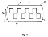
図1は、第1のレーザ印刷システム100の主要な略図を示している。レーザ印刷システム100は、半導体レーザ115を有する2つのレーザアレイ110と光学要素170とを有する。半導体レーザ115は、半導体チップ上に設けられたVCSELである。この場合、1つのアレイ110の全てのVCSEL115は、1つのチップ上に設けられる。光学要素170は、焦点距離fを有するイメージングレンズである。アレイ110は、イメージレンズによって使用面180に拡散的に結像される図の面に直交する幅Dを有する。使用面180における幅Dを有する各アレイ110の拡散像の幅dは、使用面180における画素の幅を規定する。画素dの幅は、それぞれのアレイの幅Dより小さい。それ故、アレイの像は縮小される。使用面180とイメージレンズ又は光学要素170との間の距離bは、イメージレンズの焦点距離fより大きい。光学要素170又はイメージレンズは、使用面180と一緒に、イメージレンズの焦点距離より大きい距離gにおいて対物面150を規定する。VCSEL115の発光面は、対物面に設けられるのではなく、VCSEL115の発光面の鮮明な投射が与えられないように、或る距離において対物面の後にある。VCSEL115の発光層と対物面との間の距離は、1つのレーザアレイ110の少なくとも2つのVCSEL115のレーザ光が画素のエリア要素を同時に照射する態様で選択される。図2は、対物面150に関して1つのVCSEL115により放射されたレーザ光の発散角度の配列を更に詳細に示している。
VCSEL115の発散角度は、図2に示されるように或る角度により与えられ、単一のVCSEL115により放射されるレーザ光の円錐を規定する。レーザアレイ110におけるVCSEL115は、互いに対して距離p(ピッチ)を有する。ピッチpと距離aとの間の関係は、条件

The divergence angle of the
レーザアレイ110のVCSEL115により放射されたレーザ光は、対物面150におけるレーザアレイ110と同じサイズの各エリアが少なくとも2つのVCSEL115によって照射されるように、対物面150において重複する。従って、画素サイズdにより規定される画素の各エリア要素は、それぞれのレーザアレイ110の少なくとも2つのVCSEL115によってイメージレンズを介して照射される。各レーザアレイのVCSELは、並行して駆動され、それ故レーザ光を同時に放射する。画素のサイズは、d=M*Dにより与えられる。ここで、倍率Mは、M=b/gにより与えられる。
The laser light emitted by
使用面180におけるオブジェクトへのエネルギ入力の均一性を増大させるために、及び、単一のVCSELの故障に関する信頼性を向上させるために、使用面180におけるレーザアレイ110の像は拡散する。
In order to increase the uniformity of the energy input to the object on the
レーザモジュールのレーザアレイ110と使用面180との間の全体距離は、図3に示すようにレーザアレイ110と組み合わせられ得るマイクロレンズアレイ175によって増大されてもよい。マイクロレンズアレイ175は、各VCSEL115の発散角度αを減少させるために、レーザアレイ110と対物面150との間に設けられてもよい。距離a、それ故に使用面150までの全体距離は、VCSEL115のピッチが同じのままである場合に条件
図2に関して述べられた条件の改良は、円形開口を有するVCSEL115の場合にVCSEL115のアクティブな直径vを考慮することにより実現されてもよい。アクティブな直径vは、活性層の発光エリアの直径に対応する。アクティブな直径v、ピッチp及び距離aの間の関係は、この改良された実施形態において、条件
図4は、レーザ印刷システム100のレーザモジュールにおけるレーザアレイ110の配列の主要な略図を示している。レーザ又はVCSELアレイ110は、正方形ではないが矩形であり、矩形の長辺は、オブジェクトの運動の方向に設けられる(図5を参照)。これは、横方向の解像度を低減することなく、画素毎により高い全体出力を可能にする。VCSELアレイ110は、互いに対して僅かにシフトされる2つの列に更に設けられる(カスケードされた又はずらされた配列)。これは、オブジェクトがVCSELの列の方向に直交するよう移動する場合にオブジェクトのエリア要素の照射に対する規定された重複を可能にする。
FIG. 4 shows a main schematic diagram of the array of
図5は、レーザ印刷システム100のレーザモジュールの第1の配列の主要な略図を示している。レーザモジュールは、図4に示されたレーザアレイ110及び光学要素170のずらされた又はカスケードされた配列を有する。光学要素170は、レーザ印刷システム100の使用面180に対してそれぞれのレーザモジュールの全てのレーザアレイ110を結像する。光学要素170は、レーザモジュールの全体のサイズYを規定し、それぞれのレーザモジュールのレーザアレイ110の配列の幅は、1つのレーザモジュールの印刷幅yを規定する。レーザモジュールは、互いに平行な列に設けられ、オブジェクトがレーザモジュールに対して方向250に移動する場合に連続エリアが使用面180に照射され得るように、各列がシフトされる。それ故、印刷エリアは、単一のレーザモジュールのサイズY及び印刷幅yから独立して使用面におけるオブジェクトのサイズに適合され得る。使用面180において移動するオブジェクトを継続的に照射するために必要とされる列の数は、レーザモジュールのサイズY及び印刷幅yに依存する。1つの列の範囲内のレーザモジュールは、少なくともN=Y/y列が必要とされるように、少なくとも距離Yにより分離される。カスケードされた光学要素170は、例えばガラスモールディングにより単一の部分として製作されてもよい。代わりに、レンズアレイは、能動的又は受動的な配置により個々のレンズから組み立てられてもよい。
FIG. 5 shows a main schematic diagram of a first array of laser modules of the
図6は、レーザ印刷システムのレーザモジュールの第2の配列の主要な略図を示している。配列は、図5に関して述べられた配列と非常に類似している。レーザモジュールのレーザアレイ110は、レーザモジュールに対してオブジェクトの運動250の方向に直交する方向に対して傾斜される(これらの中央の周りで回転される)。これは、図7及び図8に示されるように滑らかな傾斜を有する一体化された強度プロファイルを可能にし、これは、とりわけ画素が互いに対して僅かに整列されていない場合に、全体の強度分配の均一性を向上させるために、隣り合う画素と重複してもよい。
FIG. 6 shows a main schematic of a second arrangement of laser modules of the laser printing system. The sequence is very similar to the sequence described with respect to FIG. The
図7は、図6に示されたレーザモジュールの配列において如何なる第2の画素も伴わないレーザモジュールに対するオブジェクトの運動250の方向に直交する方向610における一体化された強度プロファイルを示している。画素形状は、隣り合う画素と重複する大きな傾斜を有する、ほぼ三角形である。図8は、図6に示されたレーザモジュールの配列におけるオン/オフ動作の切替えられた画素の任意のパターンを有する一体化された強度プロファイルを示している。数"1"及び"0"は、隣り合うレーザアレイ110のうちどれがオンであるか又はオフであるかを示す。一体化された強度プロファイルは、使用面180における2又はそれ以上の隣り合う画素の重複を示す。
FIG. 7 shows an integrated intensity profile in a
図9は、レーザ印刷の方法の方法ステップの主要な略図を示している。ステップの示されたシーケンスは、方法の実行の間に同じシーケンスを必ずしも意味するというわけではない。方法ステップは、異なる順序で又は同時に実行されてもよい。ステップ910において、1枚の紙のようなオブジェクトは、レーザモジュールに対してレーザ印刷システムの使用面において移動される。ステップ920において、レーザ光は、半導体レーザの少なくとも2つのレーザアレイと少なくとも1つの光学要素とを有するレーザモジュールによって放射される。ステップ930において、レーザアレイにより放射されるレーザ光が結像され、従って、1つのレーザアレイの半導体レーザのレーザ光は、使用面における1つの画素に結像され、画素のエリア要素は、少なくとも2つの半導体レーザによって照射される。オブジェクトが移動されてもよく、同時に、レーザアレイのレーザ光が使用面に放射及び結像されてもよい。
FIG. 9 shows the main schematic of the method steps of the laser printing method. The indicated sequence of steps does not necessarily mean the same sequence during the execution of the method. The method steps may be performed in different orders or simultaneously. In
個別に対処可能なレーザ又はレーザアレイを用いたとき、印刷、とりわけ3D印刷プロセスの最大の速度は、ラインに沿って全ての個々の画素が同時に書き込まれ得るときに、即ち画素毎の分離レーザ又はレーザアレイにより取得され得る。レーザ印刷システム又はマシンにおける典型的なライン幅は、30cm又はそれ以上のオーダーである。一方で、個別に対処可能なレーザ又はレーザアレイのレーザモジュールのサイズ又は印刷幅は、数cmに制限される。これらのレーザモジュールは、通常、レーザモジュールが設けられる1つのマイクロチャネル冷却器に対応する。 When using individually addressable lasers or laser arrays, the maximum speed of printing, especially the 3D printing process, is when all individual pixels can be written simultaneously along the line, i.e. a separate laser per pixel or It can be acquired by a laser array. Typical line widths in laser printing systems or machines are on the order of 30 cm or more. On the other hand, the size or print width of a laser module of a laser or laser array that can be individually handled is limited to a few cm. These laser modules usually correspond to one microchannel cooler in which the laser module is provided.
それ故、多数のレーザモジュール及び対応するマイクロチャネル冷却器を用いること、及び、これらを同時に完全なレーザ印刷モジュール又は印刷ヘッドにスタックすることが必要である。レーザモジュールを有する隣り合うマイクロチャネル冷却器間の配列許容誤差は、レーザ光が供給され得ないか又は充分なレーザ光が供給され得ない使用面180においてギャップをもたらし得る。最悪の場合において、斯様なギャップは、低品質の印刷シートとしてのオブジェクトの処理に関して、又は、3Dプリンタ/ラピッドプロトタイピングマシンによって生成される部分において、欠陥をもたらす。
It is therefore necessary to use a large number of laser modules and corresponding microchannel coolers and to stack them together in a complete laser printing module or printhead. The alignment tolerance between adjacent microchannel coolers with laser modules can cause gaps in the
100μmのレーザ光源116の典型的なサイズ及び幾つかの配列許容誤差が同時に加算されるという事実からみて、ギャップの問題は厳しい問題である。レーザ印刷システムを組み立てる個々のステップにおける厳しい許容誤差であっても、全体的な許容誤差チェインは、30μm又はそれ以上の重大なずれをもたらし得る。
In view of the typical size of the 100
これに関して、重なり合う強度分布を提供するだけでなく、各レーザモジュールの端において追加のレーザ光源116を用いることが有利であってもよい。前記レーザ光源116は、これらの重複レーザ光源117の光が隣り合うレーザモジュールのレーザ光源116の光と重複するように設けられる、いわゆる重複レーザ光源117である。これは、隣り合うレーザモジュール間のピッチが少なくともレーザモジュールの全体の印刷幅より小さな1つのレーザ光源116の幅(例えば100μm)によるものであることを意味する。
In this regard, it may be advantageous to use an
隣り合うレーザモジュールの機械的/光学的配列からの最大許容誤差が1つのレーザ光源116の幅より小さい場合、レーザ光が供給され得ない使用面におけるギャップを回避するために意図的に1つのレーザ光源116の重複を有することが十分である。とにかく、隣り合うレーザモジュールの機械的/光学的配置からの最大許容誤差が1つのレーザ光源116の幅より大きい場合、代わりに1つを超える重複レーザ光源117を設けることが可能であってもよい。この場合、隣り合うレーザモジュール間のギャップの幅に従って重複レーザ光源117を用いることが可能であってもよい。レーザ印刷システムは、この場合、重複レーザ光源117がレーザモジュール間の予想外のギャップを埋めるように較正されてもよい。ギャップ及び1つのレーザ光源116の幅に依存して、1,2,3又はそれよりも多くの重複レーザ光源117が使用面のシームレスな照射を可能にするために用いられることがあってもよい。
If the maximum allowable error from the mechanical / optical arrangement of adjacent laser modules is smaller than the width of one
図10は、互いに対してレーザサブモジュール120の潜在的な不整列を補正するためにレーザサブモジュール120である隣り合うレーザモジュールの重なり合う配列に設けられるレーザ光源116である重複レーザ光源117を有する斯様な配列の一実施形態を示している。重複レーザ光源117は、ラインパターンにより示される。
FIG. 10 includes an overlapping
隣り合うレーザサブモジュール120の印刷幅は、完全なレーザ光源116又はより明示的な重複レーザ光源117により重複する。レーザ光源116は、前の実施形態とは異なり単一のレーザのみを有してもよく、又は、前の実施形態に従って、レーザアレイ110のようなレーザアレイを有してもよい。単一のレーザは、マイクロレンズのような光学要素を有してもよい。レーザアレイの場合、マイクロレンズアレイが含まれてもよい。レーザサブモジュール120の配列は、図5に示された配列と同様である。図5に示されたレーザモジュールは、各レーザアレイ110が使用面180における専用の画素又はエリア要素を照射するように構成される。図10に示されたレーザサブモジュール120は、隣り合うレーザサブモジュール120のレーザ光源116と同じ、使用面180におけるエリア要素を照射し得るように、組立ての間に配列誤差がない場合において重複レーザ光源117が適合されるように構成される。
The print widths of
図11は、図5と同様のレーザモジュールの配列を示しており、2つを超える列及び使用面180において光学要素を有するレーザモジュールにより生成される縮小された像が示される点が異なる。図11に概略的に示されるように、レーザモジュールの配列は、運動250の方向に直交する列に設けられた複数のレーザモジュール200を含む。図5及び図6と同様に、レーザモジュールの第1の列c1の第1のレーザモジュール2001が使用面180における第1のエリアy1を照射するように適合されるように、レーザモジュールの列が互いに対してずらされる。レーザモジュールの第2の列c2の第2のモジュール2002は、使用面180における第2のエリアy2を照射するように適合され、第1のエリアy1は、オブジェクトの連続的な照射が可能になるように、第2のエリアy2と隣り合う。これによって、使用面180における照射されたエリアy1,y2は、運動の方向に直交する方向において隣接するエリアを形成する。図11に更に示されるように、運動250の方向にずらされたレーザモジュールはカスケードを形成する。第1のカスケードk1は、列の第1のレーザモジュール2001,2002,200nにより形成される。第2のカスケードk2は、列の第2のレーザモジュール2011,2012,201nにより形成される等である。カスケードの数は、運動250の方向に直交する方向における個々の印刷幅yの合計が使用面において照射されるべき全体エリアを覆うようになっている。
FIG. 11 shows an arrangement of laser modules similar to FIG. 5, except that a reduced image produced by a laser module having optical elements in more than two rows and use surfaces 180 is shown. As schematically shown in FIG. 11, the array of laser modules includes a plurality of
好ましくは、モジュール200のレーザアレイ110は、図4に示されるように設けられる。更に好ましい実施形態において、レーザアレイ110の斯様な配列に関連付けられた光学要素175は、両面が切り取られた円形又は回転対称の外形から取得される外形を有し、光学要素175の両面lは、好ましくは運動250の方向に直交する方向に配向される軸に沿って互いに位置調整される。より正確に言うと、図4のようなレーザアレイの配列の場合、光学要素175は、平行な長辺lに接続する2つの対向する円形セグメント状の短辺sを有する変更された矩形の輪郭を有する。これは、円形光学要素が図4に示されたレーザアレイの矩形配列によって完全には照射されないことを考慮する。それ故、完全には照明されない円形光学要素の部分は省略され得る。光学要素175の形状によって、運動250の方向のモジュールのサイズが低減され得る。その結果として、運動250の方向におけるレーザモジュールの配列のサイズが低減され得る。これは、運動の方向に配向されるラインが3D印刷システム全体の生産性を強化する低減された時間の範囲内で照射され得るという利点を有する。また、1つのカスケードk1の1つのモジュール2001と隣り合うモジュール2002との間の、及び/又は、1つのカスケードk1の1つのモジュール200nと隣り合うカスケードk2の隣り合うモジュール2011との間の、境界における隣り合う画素は、低減された時間オフセットにより照射され得る。これは、三次元物品の品質を増大させる。
Preferably, the
レーザアレイ110におけるVCSELの配列は、強度プロファイルを規定する。配列が実質的に矩形である場合、即ちVCSELが行及び列のアレイに設けられる場合、アレイの一体化された強度プロファイル600は実質的に矩形である、即ち一体化された強度プロファイルは、図14に示されるようないわゆる"フラットトップ"プロファイルを有する。幾つかのアレイ110がオンにされるとともに幾つかのアレイがオフにされる、図4によるモジュールにおいて、運動250の方向に直交する方向610におけるモジュールの一体化された強度は、図15に示されるようなもの、即ち鮮明なエッジを有する。
The arrangement of VCSELs in
鮮明なエッジを伴うことなく一体化された強度プロファイルを有することが望ましいかもしれない。これは、図13による配列により実現され得る。ここで、1つのアレイ110におけるVCSELは、行及び列に配置され、アレイの外形形状は、実質的に多角形、とりわけ実質的に六角形である。個々のVCSELは、1つの列から隣の列までずらされるグリッドポイントに配置され、列は、運動250の方向に直交するよう配向される。好ましくは、アレイの外形形状は、運動250の方向に直交するよう延在する2つの対向する平行面pを有する六角形の形状を有する。
It may be desirable to have an integrated intensity profile without sharp edges. This can be realized by the arrangement according to FIG. Here, the VCSELs in one
図16に示されるように、図13に示された実質的に六角形の形状を有するレーザアレイの一体化された強度プロファイル600は丸い端を有し、ガウス強度分布と同様である。切替えられたオン/オフ動作のアレイを有するレーザモジュールに関して、方向610に沿った一体化された強度プロファイル600は、図17に示された丸い遷移を有する。それ故、強度の平均値からのずれはより小さくなる。
As shown in FIG. 16, the
レーザモジュールの配列によれば、作業エリアにおける1つの画素は、レーザアレイ110の多数の半導体レーザにより同時に照射される。半導体レーザの全体数は、予め決められた数の半導体レーザより少ないという失敗が予め決められた許容誤差値の範囲内でのみレーザアレイ110の出力を低減させるように選択されてもよい。その結果として、個々のVCSELの動作寿命に関する要件は、異常に高くならないかもしれない。
According to the arrangement of the laser modules, one pixel in the work area is irradiated simultaneously by a number of semiconductor lasers in the
レーザアレイの個々のVCSELは、制御信号によりこれらの対処能力に関してサブグループにおいてグループ化されてもよい。サブグループは、少なくとも2つのVCSELを含んでもよい。1つのレーザアレイのVCSELの少なくとも2つのサブグループは、レーザアレイ110の出力がVCSELの1又はそれ以上のサブグループのスイッチをオフにすることにより制御可能であるように、個別に対処可能であってもよい。また、レーザアレイの出力が個々の半導体レーザをオン/オフにすることにより制御され得るように1つのレーザアレイの半導体レーザが個別に対処可能である一実施形態が提供されてもよい。
The individual VCSELs of the laser array may be grouped in subgroups with respect to their coping capabilities by control signals. A subgroup may include at least two VCSELs. At least two subgroups of VCSELs in one laser array can be individually addressed so that the output of
更なる実施形態において、レーザモジュールの配列のレーザアレイ又は半導体レーザは、照射するために用いられないレーザアレイ又は半導体レーザが使用面180における材料に熱を与えるためにオプションとして用いられ得るように、更に制御され得る。これを達成するために、半導体レーザ又はレーザアレイを個別に制御する制御デバイスが提供される。この加熱は、前記の分離加熱デバイスに加えて、又は、動作温度までオブジェクトを予熱する排他的加熱システムとして用いられ得る。
In a further embodiment, a laser array or semiconductor laser in an array of laser modules may be used as an option to provide heat to the material at the
レーザモジュールの配列は、図10を参照して説明される重複光源117を含んでもよい。重複光源117は、隣り合う列の隣り合うモジュールに対する1つの列の1つのモジュール、例えば列c1のモジュール2001と、図13における列c2のモジュール2002との間の、及び/又は、隣り合うカスケードにおける隣り合うモジュールに対する1つのカスケードにおける1つのモジュール、例えばカスケードk1におけるモジュール200nと図11におけるカスケードk2におけるモジュール2011との間の、境界に好ましくは設けられる。重複光源117は、モジュールのずらされた配列に起因して及び/又はモジュールのカスケードされた配列に起因して、運動250の方向に直交する隣り合う画素の時間オフセットから生じるエネルギ損失のバランスをとる。
The array of laser modules may include overlapping
重複光源117は、時間オフセットに起因したエネルギ損失及び/又はVCSEL若しくはアレイの不整列に起因したエネルギ損失若しくはエネルギ超過が補正され得るような態様で制御され得る。それ故、重複光源117による動作エリアに与えられるエネルギの合計は、完全に位置調整されたVCSEL若しくはアレイ及び/又は時間オフセットゼロの場合に照射するために必要なエネルギになるように調整され得る。重なり合うVCSEL又はアレイにより与えられるエネルギは、形成材料のタイプに依存して選択され得る。影響する因子は、オブジェクトの熱伝導率であってもよい。
The overlapping
更なる変形例において、照射ユニットの半導体レーザは、VECSEL(Vertical External Cavity Surface Emitting Laser)により実現される。 In a further modification, the semiconductor laser of the irradiation unit is realized by VECSEL (Vertical External Cavity Surface Emitting Laser).
本発明が図面及び前述の説明において詳細に示され、述べられた一方で、斯様な図及び説明は、例証又は例示的であり、限定的ではないものと見なされるべきである。 While the invention has been illustrated and described in detail in the drawings and foregoing description, such illustration and description are to be considered illustrative or exemplary and not restrictive.
本開示を読みとることから、他の変形が当業者にとって明らかになるだろう。斯様な変形は、従来技術において既に知られている他の特徴、及び、ここで既に述べられた特徴の代わりに又はそれに加えて用いられ得る他の特徴を含んでもよい。 From reading the present disclosure, other modifications will be apparent to persons skilled in the art. Such variations may include other features already known in the prior art, and other features that may be used in place of or in addition to features already described herein.
開示された実施形態のバリエーションは、図面、開示及び添付の特許請求の範囲の研究から、当業者により理解され、遂行され得る。請求項において、"有する"という用語は、他の要素又はステップを除外するものではなく、単数表記は、複数の要素又はステップを除外するものではない。特定の手段が相互に異なる従属請求項に記載されるという単なる事実は、これらの手段の組み合わせが有効に用いられ得ないことを示すものではない。 Variations of the disclosed embodiments can be understood and carried out by those skilled in the art from a study of the drawings, the disclosure, and the appended claims. In the claims, the term “comprising” does not exclude other elements or steps, and the singular form does not exclude a plurality of elements or steps. The mere fact that certain measures are recited in mutually different dependent claims does not indicate that a combination of these measured cannot be used to advantage.
請求項中の任意の参照符号は、その範囲を限定するものとして解釈されるべきでない。 Any reference signs in the claims should not be construed as limiting the scope.
100 レーザ印刷システム
110 レーザアレイ
115 半導体レーザ
116 レーザ光源
117 重複レーザ光源
120 レーザサブモジュール
150 対物面
170 光学要素
175 マイクロレンズアレイ
180 使用面
200,2001,2002,200n,2011,2012,201n レーザモジュール
250 運動の方向
600 一体化された強度
610 運動の方向に直交する方向
750 保護デバイス
800 制御ユニット
910 オブジェクトの方法ステップ
920 レーザ光を放射する方法ステップ
930 レーザ光を結像する方法ステップ
100
Claims (15)
前記レーザモジュールは、半導体レーザの少なくとも2つのレーザアレイと、少なくとも1つの光学要素とを有し、前記光学要素は、1つのレーザアレイの半導体レーザのレーザ光が当該レーザ印刷システムの前記使用面における1つの画素に対して結像されるとともに前記画素のエリア要素が少なくとも2つの半導体レーザによって照射されるように、前記レーザアレイにより放射されたレーザ光を結像するように適合され、
前記光学要素は、隣り合う半導体レーザにより放射されるレーザ光の円錐が前記使用面に対する前記光学要素の対物面において重なるように、前記対物面が前記半導体レーザの発光層と一致しない態様で設けられる、レーザ印刷システム。 A laser printing system for irradiating an object that moves relative to a laser module of a laser printing system on a use surface,
The laser module includes at least two laser arrays of semiconductor lasers and at least one optical element, and the optical element is configured such that the laser light of the semiconductor laser of one laser array is emitted from the use surface of the laser printing system. Adapted to image the laser light emitted by the laser array so that it is imaged on one pixel and the area elements of the pixel are illuminated by at least two semiconductor lasers;
The optical element is provided in such a manner that the objective surface does not coincide with the light emitting layer of the semiconductor laser so that a cone of laser light emitted by an adjacent semiconductor laser overlaps the objective surface of the optical element with respect to the use surface. , Laser printing system.
前記マイクロレンズアレイは、前記半導体レーザにより放射されるレーザ光の発散を低下させるように構成される、請求項1に記載のレーザ印刷システム。 Each laser array has a microlens array,
The laser printing system of claim 1, wherein the microlens array is configured to reduce divergence of laser light emitted by the semiconductor laser.
各レーザモジュールは、少なくとも2つのレーザアレイを有し、
前記第1又は第2のレーザモジュールの2つのレーザアレイのうち少なくとも1つは、動作中、前記使用面における少なくとも1つの規定されたエリア要素が重複レーザ光源及び前記重複レーザ光源を有するレーザモジュールの隣に設けられたレーザモジュールのレーザアレイにより照射され得るように、前記重複レーザ光源として設けられる、請求項1に記載のレーザ印刷システム。 Having at least first and second laser modules provided next to each other;
Each laser module has at least two laser arrays,
At least one of the two laser arrays of the first or second laser module is configured such that, during operation, at least one defined area element on the use surface includes an overlapping laser light source and the overlapping laser light source. The laser printing system according to claim 1, wherein the laser printing system is provided as the overlapping laser light source so as to be irradiated by a laser array of a laser module provided next to the laser module.
半導体レーザの少なくとも2つのレーザアレイと少なくとも1つの光学要素とを有する前記レーザモジュールによってレーザ光を放射するステップと、
1つのレーザアレイの半導体レーザのレーザ光が前記使用面における1つの画素に結像されるとともに、前記画素のエリア要素が少なくとも2つの半導体レーザによって照射されるように、前記光学要素によって前記レーザアレイにより放射されたレーザ光を結像するステップとを有し、
前記光学要素は、隣り合う半導体レーザにより放射されたレーザ光の円錐が前記使用面に対する前記光学要素の対物面において重複するように、前記対物面が前記半導体レーザの発光層と一致しない態様で設けられる、レーザ印刷の方法。 Moving an object on the use surface relative to the laser module;
Emitting laser light by the laser module having at least two laser arrays of semiconductor lasers and at least one optical element;
Laser light from a semiconductor laser of one laser array is imaged on one pixel on the use surface, and the optical element causes the laser array to irradiate an area element of the pixel with at least two semiconductor lasers. Imaging the laser light emitted by
The optical element as conical laser emitted by the semiconductor laser adjacent light overlap in pairs Object plane of the optical element relative to the working surfaces, in a manner that the object plane does not coincide with the light-emitting layer of the semiconductor laser A method of laser printing provided.
Applications Claiming Priority (3)
| Application Number | Priority Date | Filing Date | Title |
|---|---|---|---|
| EP13197751 | 2013-12-17 | ||
| EP13197751.4 | 2013-12-17 | ||
| PCT/EP2014/077931 WO2015091459A1 (en) | 2013-12-17 | 2014-12-16 | Laser printing system |
Publications (3)
| Publication Number | Publication Date |
|---|---|
| JP2017501052A JP2017501052A (en) | 2017-01-12 |
| JP2017501052A5 JP2017501052A5 (en) | 2018-03-22 |
| JP6310560B2 true JP6310560B2 (en) | 2018-04-11 |
Family
ID=49886642
Family Applications (3)
| Application Number | Title | Priority Date | Filing Date |
|---|---|---|---|
| JP2016538064A Active JP6310560B2 (en) | 2013-12-17 | 2014-12-16 | Laser printing system |
| JP2016539227A Active JP6585597B2 (en) | 2013-12-17 | 2014-12-16 | Laser printing system |
| JP2019119534A Active JP6810199B2 (en) | 2013-12-17 | 2019-06-27 | Laser printing system |
Family Applications After (2)
| Application Number | Title | Priority Date | Filing Date |
|---|---|---|---|
| JP2016539227A Active JP6585597B2 (en) | 2013-12-17 | 2014-12-16 | Laser printing system |
| JP2019119534A Active JP6810199B2 (en) | 2013-12-17 | 2019-06-27 | Laser printing system |
Country Status (10)
| Country | Link |
|---|---|
| US (5) | US10723139B2 (en) |
| EP (3) | EP3083254B1 (en) |
| JP (3) | JP6310560B2 (en) |
| KR (1) | KR102283851B1 (en) |
| CN (3) | CN105829113B (en) |
| BR (1) | BR112016013879A2 (en) |
| ES (1) | ES2799123T3 (en) |
| MX (1) | MX2016007805A (en) |
| RU (2) | RU2656205C1 (en) |
| WO (2) | WO2015091485A1 (en) |
Families Citing this family (122)
| Publication number | Priority date | Publication date | Assignee | Title |
|---|---|---|---|---|
| GB0816308D0 (en) | 2008-09-05 | 2008-10-15 | Mtt Technologies Ltd | Optical module |
| WO2015091485A1 (en) * | 2013-12-17 | 2015-06-25 | Eos Gmbh Electro Optical Systems | Laser printing system |
| US10029421B2 (en) * | 2014-09-18 | 2018-07-24 | 3Dm Digital Manufacturing Ltd | Device and a method for 3D printing and manufacturing of materials using quantum cascade lasers |
| DE102015200134A1 (en) * | 2015-01-08 | 2016-07-14 | Trumpf Laser- Und Systemtechnik Gmbh | Modular SLM or SLS processing machine |
| US20180056585A1 (en) * | 2015-05-12 | 2018-03-01 | Gizmo 3D Printers | Improvements in 3d printing |
| IL255928B (en) * | 2015-05-27 | 2022-08-01 | Landa Labs 2012 Ltd | Imaging device |
| JP6505517B2 (en) * | 2015-06-18 | 2019-04-24 | ローランドディー.ジー.株式会社 | Three-dimensional modeling device |
| WO2017013242A1 (en) * | 2015-07-23 | 2017-01-26 | Koninklijke Philips N.V. | Laser printing system |
| DE102015115810A1 (en) | 2015-09-18 | 2017-03-23 | Osram Opto Semiconductors Gmbh | Optoelectronic semiconductor device and 3D printer |
| DE102015219866A1 (en) | 2015-10-13 | 2017-04-13 | Eos Gmbh Electro Optical Systems | Device and method for producing a three-dimensional object |
| WO2017075244A1 (en) | 2015-10-30 | 2017-05-04 | Seurat Technologies, Inc. | Additive manufacturing system and method |
| DE102015221623A1 (en) | 2015-11-04 | 2017-05-04 | Eos Gmbh Electro Optical Systems | Exposure optics and apparatus for producing a three-dimensional object |
| JP2019504182A (en) * | 2015-11-16 | 2019-02-14 | レニショウ パブリック リミテッド カンパニーRenishaw Public Limited Company | Module and method for additive manufacturing equipment |
| US10471543B2 (en) * | 2015-12-15 | 2019-11-12 | Lawrence Livermore National Security, Llc | Laser-assisted additive manufacturing |
| US11850791B2 (en) | 2016-01-20 | 2023-12-26 | Hewlett-Packard Development Company, L.P. | Printing devices |
| WO2017132664A1 (en) | 2016-01-28 | 2017-08-03 | Seurat Technologies, Inc. | Additive manufacturing, spatial heat treating system and method |
| EP3995277A1 (en) | 2016-01-29 | 2022-05-11 | Seurat Technologies, Inc. | System for additive manufacturing |
| CN109070221B (en) * | 2016-04-25 | 2021-08-03 | 瑞尼斯豪公司 | Method of calibrating a plurality of scanners in an additive manufacturing apparatus |
| EP3458251A4 (en) * | 2016-05-17 | 2020-01-08 | Hewlett-Packard Development Company, L.P. | 3d printer with tuned fusing radiation emission |
| US10717230B2 (en) * | 2016-06-16 | 2020-07-21 | Xerox Corporation | Line laser imager for thermoplastic selective laser sintering |
| KR101787718B1 (en) * | 2016-06-21 | 2017-11-16 | 한국기계연구원 | 3-dimensional laser printing apparatus and method |
| WO2018015075A1 (en) * | 2016-07-20 | 2018-01-25 | Sintratec Ag | Protection element |
| CN106216862B (en) * | 2016-07-20 | 2018-10-16 | 华中科技大学 | A kind of composite manufacturing method and device subtracting material based on electric arc increasing material and high energy beam current |
| US10821717B2 (en) | 2016-07-22 | 2020-11-03 | General Electric Company | Layer orientation control for pixel-based additive manufacturing |
| US10953470B2 (en) | 2016-08-31 | 2021-03-23 | Raytheon Technologies Corporation | Scanning mirror navigation apparatus and method |
| CN106229808B (en) * | 2016-09-20 | 2023-08-29 | 中国电子科技集团公司第十三研究所 | Pulse laser |
| DE102016218887A1 (en) * | 2016-09-29 | 2018-03-29 | SLM Solutions Group AG | Producing three-dimensional workpieces by means of a plurality of irradiation units |
| JP2018059757A (en) * | 2016-10-04 | 2018-04-12 | オムロンオートモーティブエレクトロニクス株式会社 | Light projection optical system and object detector |
| DE102016120044A1 (en) * | 2016-10-20 | 2018-04-26 | Cl Schutzrechtsverwaltungs Gmbh | Device for the additive production of three-dimensional objects |
| FR3057793B1 (en) * | 2016-10-26 | 2021-04-09 | Fives Michelin Additive Solutions | APPARATUS AND METHOD FOR MANUFACTURING A THREE-DIMENSIONAL OBJECT |
| FR3057794B1 (en) * | 2016-10-26 | 2019-07-19 | Addup | IMPROVEMENTS IN SELECTIVE ADDITIVE MANUFACTURING |
| US10919285B2 (en) * | 2016-11-07 | 2021-02-16 | General Electric Company | Method and system for x-ray backscatter inspection of additive manufactured parts |
| DE102016222187A1 (en) * | 2016-11-11 | 2018-05-17 | Trumpf Laser- Und Systemtechnik Gmbh | Method for determining a beam profile of a laser beam and processing machine |
| DE102016123000B3 (en) * | 2016-11-29 | 2017-12-14 | Scansonic Mi Gmbh | Method for monitoring a protective glass and monitoring device |
| US10399179B2 (en) * | 2016-12-14 | 2019-09-03 | General Electric Company | Additive manufacturing systems and methods |
| US10589508B2 (en) | 2016-12-15 | 2020-03-17 | General Electric Company | Additive manufacturing systems and methods |
| US10583530B2 (en) | 2017-01-09 | 2020-03-10 | General Electric Company | System and methods for fabricating a component with laser array |
| US10549519B2 (en) * | 2017-01-12 | 2020-02-04 | Caterpillar Inc. | Systems and methods for calibrating additive manufacturing operations based on energy density |
| GB201701355D0 (en) | 2017-01-27 | 2017-03-15 | Renishaw Plc | Direct laser writing and chemical etching |
| US11548094B2 (en) * | 2017-02-15 | 2023-01-10 | General Electric Company | System and methods for fabricating a component with laser array |
| US10317881B2 (en) | 2017-03-01 | 2019-06-11 | General Electric Company | Parallelized CAD using multi laser additive printing |
| US10695865B2 (en) * | 2017-03-03 | 2020-06-30 | General Electric Company | Systems and methods for fabricating a component with at least one laser device |
| JP6844347B2 (en) * | 2017-03-15 | 2021-03-17 | 株式会社リコー | Laser processing equipment |
| EP3382828A1 (en) * | 2017-03-31 | 2018-10-03 | Koninklijke Philips N.V. | Inherently safe laser arrangement comprising a vertical cavity surface emitting laser |
| US10906132B2 (en) * | 2017-03-31 | 2021-02-02 | General Electric Company | Scan strategies for efficient utilization of laser arrays in direct metal laser melting (DMLM) |
| KR102515643B1 (en) | 2017-05-11 | 2023-03-30 | 쇠라 테크널러지스 인코포레이티드 | Switchyard beam routing of patterned light for additive manufacturing |
| DE102017210994A1 (en) | 2017-06-28 | 2019-01-03 | Eos Gmbh Electro Optical Systems | Measuring system for a device for the generative production of a three-dimensional object |
| US10882248B2 (en) * | 2017-06-28 | 2021-01-05 | 3D Systems, Inc. | Three dimensional printer for fusing powders with surface coloration using a VCSEL array |
| US11407034B2 (en) | 2017-07-06 | 2022-08-09 | OmniTek Technology Ltda. | Selective laser melting system and method of using same |
| WO2019022755A1 (en) * | 2017-07-28 | 2019-01-31 | Hewlett-Packard Development Company, L.P. | Three-dimensional printer with movement device |
| GB201712726D0 (en) * | 2017-08-08 | 2017-09-20 | Landa Labs (2012) Ltd | Electric current and heat mitigation in a printing machine writing module |
| US10766242B2 (en) * | 2017-08-24 | 2020-09-08 | General Electric Company | System and methods for fabricating a component using a consolidating device |
| CN107457986A (en) * | 2017-08-26 | 2017-12-12 | 吴江中瑞机电科技有限公司 | The circulating photocuring 3D printer of ultrahigh speed |
| EP3451470A1 (en) | 2017-08-30 | 2019-03-06 | Koninklijke Philips N.V. | Laser arrangement comprising a vcsel array |
| JP6642546B2 (en) * | 2017-09-21 | 2020-02-05 | 日亜化学工業株式会社 | Wavelength beam combiner |
| TWI719261B (en) | 2017-09-29 | 2021-02-21 | 國立中興大學 | Apparatus of additive manufacturing using optical pickup head |
| US11084132B2 (en) | 2017-10-26 | 2021-08-10 | General Electric Company | Diode laser fiber array for contour of powder bed fabrication or repair |
| WO2019099928A2 (en) * | 2017-11-17 | 2019-05-23 | Kevin Friesth | Advanced automated fabrication system and methods for thermal and mechanical components utilizing quadratic or squared hybrid direct laser sintering, direct metal laser sintering, cnc, thermal spraying, direct metal deposition and frictional stir welding |
| US11027336B2 (en) * | 2017-11-21 | 2021-06-08 | Hamilton Sundstrand Corporation | Splatter shield systems and methods for additive manufacturing |
| CN109940879B (en) * | 2017-12-20 | 2023-08-29 | 广州中国科学院先进技术研究所 | Novel control system and method for visible light curing 3D printer |
| EP3509170A1 (en) * | 2018-01-05 | 2019-07-10 | Koninklijke Philips N.V. | Energy efficient laser arrangement |
| WO2019143314A1 (en) * | 2018-01-16 | 2019-07-25 | Hewlett-Packard Development Company, L.P. | Three dimensional printing system |
| EP3518356A1 (en) * | 2018-01-24 | 2019-07-31 | Koninklijke Philips N.V. | Laser arrangement with irregular emission pattern |
| EP3524409A1 (en) * | 2018-02-09 | 2019-08-14 | CL Schutzrechtsverwaltungs GmbH | Apparatus for additively manufacturing three-dimensional objects |
| JP6920540B2 (en) * | 2018-03-23 | 2021-08-18 | Primetals Technologies Japan株式会社 | Laser processing head, laser processing equipment, and adjustment method of laser processing head |
| US10875094B2 (en) * | 2018-03-29 | 2020-12-29 | Vulcanforms Inc. | Additive manufacturing systems and methods |
| EP3552806A1 (en) | 2018-04-09 | 2019-10-16 | Nederlandse Organisatie voor toegepast- natuurwetenschappelijk onderzoek TNO | Method of apparatus for forming an object by means of additive manufacturing |
| CN108581215B (en) * | 2018-05-14 | 2020-01-31 | 苏州米氪激光技术服务有限公司 | staggered laser engraving equipment for processing double-pattern carpet |
| GB201807830D0 (en) | 2018-05-15 | 2018-06-27 | Renishaw Plc | Laser beam scanner |
| WO2019236106A1 (en) * | 2018-06-08 | 2019-12-12 | Hewlett-Packard Development Company, L.P. | Printing devices |
| EP3588702A1 (en) * | 2018-06-26 | 2020-01-01 | Koninklijke Philips N.V. | Vcsel array with small pulse delay |
| US11241823B2 (en) | 2018-07-10 | 2022-02-08 | 3D Systems, Inc. | Three dimensional (3D) printer with high resolution light engine |
| US11325299B2 (en) | 2018-07-16 | 2022-05-10 | Massachusetts Institute Of Technology | Additive manufacturing via optical aperture division multiplexing |
| EP3598591A1 (en) * | 2018-07-17 | 2020-01-22 | Koninklijke Philips N.V. | Laser arrangement with reduced building height |
| DE102018211972B4 (en) * | 2018-07-18 | 2020-04-23 | Trumpf Laser Gmbh | Optical arrangement for the variable generation of a multifocal profile, as well as methods for operating and using such an arrangement |
| US11167375B2 (en) | 2018-08-10 | 2021-11-09 | The Research Foundation For The State University Of New York | Additive manufacturing processes and additively manufactured products |
| US11872757B2 (en) * | 2018-10-30 | 2024-01-16 | Hewlett-Packard Development Company, L.P. | Microwave energy emitters with tips |
| KR20200053320A (en) | 2018-11-08 | 2020-05-18 | 삼성전자주식회사 | holographic display apparatus including the same |
| DE102018219302A1 (en) | 2018-11-12 | 2020-05-14 | Eos Gmbh Electro Optical Systems | Selective sintering of polymer-based building materials |
| DE102018219303A1 (en) | 2018-11-12 | 2020-05-14 | Eos Gmbh Electro Optical Systems | Warp-optimized plastic powder |
| KR102130343B1 (en) * | 2018-11-14 | 2020-08-06 | 한국기계연구원 | Apparatus for manufacturing three dimensional shapes using laser and powder |
| WO2020121959A1 (en) * | 2018-12-14 | 2020-06-18 | 株式会社デンソー | Optical distance measurement device, laser light emission device, and method for manufacturing same |
| JP7172963B2 (en) * | 2018-12-14 | 2022-11-16 | 株式会社デンソー | Optical distance measuring device, method for manufacturing laser light emitting device |
| KR20210104062A (en) | 2018-12-19 | 2021-08-24 | 쇠라 테크널러지스 인코포레이티드 | Additive Manufacturing Systems Using Pulsed Modulated Lasers for Two-Dimensional Printing |
| KR102171814B1 (en) * | 2018-12-28 | 2020-10-29 | 한국광기술원 | 3D printer |
| WO2020154703A1 (en) * | 2019-01-24 | 2020-07-30 | Walter Voit | Systems, methods, and materials for ultra-high throughput additive manufacturing |
| CN111654680A (en) * | 2019-03-04 | 2020-09-11 | 安世亚太科技股份有限公司 | Projection splicing method and device of digital light processing optical machine |
| DE102019204032B4 (en) * | 2019-03-25 | 2021-09-30 | Fraunhofer-Gesellschaft zur Förderung der angewandten Forschung e.V. | Device for generating a spatially modulatable power density distribution from laser radiation |
| CN109986079B (en) * | 2019-03-29 | 2020-04-14 | 西北大学 | Laser linear array 3D metal printer and file conversion and printing control method thereof |
| CN110142406B (en) * | 2019-03-29 | 2020-05-19 | 西北大学 | Two-dimensional optical fiber area array high-precision laser 3D metal printer and printing control method thereof |
| EP3722075B1 (en) | 2019-04-08 | 2022-06-29 | LayerWise N.V. | Three-dimensional printing system optimizing seams between zones for multiple energy beams |
| EP3748287B1 (en) * | 2019-06-06 | 2021-10-13 | TRUMPF Photonic Components GmbH | Vcsel based pattern projector |
| US11230058B2 (en) | 2019-06-07 | 2022-01-25 | The Boeing Company | Additive manufacturing using light source arrays to provide multiple light beams to a build medium via a rotatable reflector |
| CN110899986B (en) * | 2019-08-16 | 2022-02-01 | 广东省广袤科技有限公司 | Method and device for manufacturing two-dimensional code by laser scanning etching |
| CN110412544A (en) * | 2019-08-23 | 2019-11-05 | 上海禾赛光电科技有限公司 | Laser transmitting system and laser radar including the laser transmitting system |
| CN110524874B (en) * | 2019-08-23 | 2022-03-08 | 源秩科技(上海)有限公司 | Photocuring 3D printing device and printing method thereof |
| KR102367742B1 (en) * | 2019-12-10 | 2022-02-25 | (주)캐리마 | Light source Device of line shape and 3D Printer comprising the same |
| JP7463782B2 (en) * | 2020-03-17 | 2024-04-09 | 富士フイルムビジネスイノベーション株式会社 | Light emitting element array, light emitting device, optical device, measuring device, and information processing device |
| CN111605191A (en) * | 2020-06-24 | 2020-09-01 | 深圳市智能派科技有限公司 | Multi-size photocuring 3D printer concatenation light source |
| US20220062998A1 (en) * | 2020-08-27 | 2022-03-03 | Apple Inc. | Novel architectures for high-throughput additive manufacturing |
| CN113001988B (en) * | 2021-03-12 | 2021-11-12 | 江苏乾度智造高科技有限公司 | Three-dimensional printing device and method |
| IT202100008102A1 (en) | 2021-04-01 | 2021-07-01 | 3D New Tech S R L | Multi laser system for additive manufacturing |
| WO2022240397A1 (en) * | 2021-05-12 | 2022-11-17 | Hewlett-Packard Development Company, L.P. | Print agent coverage amounts |
| IT202100013136A1 (en) | 2021-05-21 | 2021-08-21 | 3D New Tech S R L | Multi laser system for additive manufacturing |
| US11951679B2 (en) | 2021-06-16 | 2024-04-09 | General Electric Company | Additive manufacturing system |
| US11599084B2 (en) * | 2021-06-18 | 2023-03-07 | Kyndryl, Inc. | Early notification system of degradation of 3D printed parts |
| US11731367B2 (en) | 2021-06-23 | 2023-08-22 | General Electric Company | Drive system for additive manufacturing |
| US11958249B2 (en) | 2021-06-24 | 2024-04-16 | General Electric Company | Reclamation system for additive manufacturing |
| US11958250B2 (en) | 2021-06-24 | 2024-04-16 | General Electric Company | Reclamation system for additive manufacturing |
| US11826950B2 (en) | 2021-07-09 | 2023-11-28 | General Electric Company | Resin management system for additive manufacturing |
| WO2023287405A1 (en) * | 2021-07-14 | 2023-01-19 | Hewlett-Packard Development Company, L.P. | Lattice cell modifications |
| DE102021208911A1 (en) | 2021-08-13 | 2023-02-16 | Eos Gmbh Electro Optical Systems | Improving the positional accuracy of the power supply in an additive manufacturing device |
| US20230054034A1 (en) * | 2021-08-23 | 2023-02-23 | Palo Alto Research Center Incorporated | 3d package for semiconductor thermal management |
| US11827037B2 (en) * | 2021-08-23 | 2023-11-28 | Xerox Corporation | Semiconductor array imager for printing systems |
| US20230056905A1 (en) * | 2021-08-23 | 2023-02-23 | Palo Alto Research Center Incorporated | Independently-addressable high power surface-emitting laser array with tight-pitch packing |
| US11813799B2 (en) | 2021-09-01 | 2023-11-14 | General Electric Company | Control systems and methods for additive manufacturing |
| WO2023059618A1 (en) | 2021-10-07 | 2023-04-13 | Additive Monitoring Systems, Llc | Structured light part quality monitoring for additive manufacturing and methods of use |
| WO2023075797A1 (en) * | 2021-10-29 | 2023-05-04 | Hewlett-Packard Development Company, L.P. | Flexible structures |
| US11987008B2 (en) | 2022-01-11 | 2024-05-21 | General Electric Company | Irradiation sequences for consolidating powder material in an additive manufacturing machine |
| CN114536772B (en) * | 2022-04-21 | 2022-07-12 | 南京铖联激光科技有限公司 | Intelligent partition control system in 3D printing system and control method thereof |
| KR20240025737A (en) * | 2022-08-19 | 2024-02-27 | 한국전자기술연구원 | Tool path generation method according to the tool path pattern area for minimizing unequal distribution of heat |
| CN117428210B (en) * | 2023-12-20 | 2024-03-08 | 中国商用飞机有限责任公司 | Multi-laser selective fusion lapping method |
Family Cites Families (29)
| Publication number | Priority date | Publication date | Assignee | Title |
|---|---|---|---|---|
| US5745153A (en) * | 1992-12-07 | 1998-04-28 | Eastman Kodak Company | Optical means for using diode laser arrays in laser multibeam printers and recorders |
| US5940113A (en) | 1994-12-19 | 1999-08-17 | Xerox Corporation | Lensless printing system with a light bar printhead |
| EP0781661A1 (en) | 1995-12-22 | 1997-07-02 | Xerox Corporation | Increased pixel density and increased printing speed in a xerographic line printer with multiple linear arrays of surface emitting lasers |
| CN1299167A (en) * | 1999-08-30 | 2001-06-13 | 贝尔-福斯公司 | Socket using resistance element for applying plug discharging |
| US6393038B1 (en) * | 1999-10-04 | 2002-05-21 | Sandia Corporation | Frequency-doubled vertical-external-cavity surface-emitting laser |
| US6264981B1 (en) | 1999-10-27 | 2001-07-24 | Anesta Corporation | Oral transmucosal drug dosage using solid solution |
| US6353502B1 (en) | 2000-06-13 | 2002-03-05 | Eastman Kodak Company | VCSEL field correction |
| JP2002019177A (en) | 2000-07-06 | 2002-01-23 | Seiko Epson Corp | Optical printer head |
| JP2002316363A (en) * | 2001-02-16 | 2002-10-29 | Fuji Photo Film Co Ltd | Optical shaping device and exposure unit |
| DE10111871A1 (en) * | 2001-03-13 | 2002-09-19 | Heidelberger Druckmasch Ag | Imaging device for a printing form with an array of VCSEL light sources |
| CN100463484C (en) * | 2001-03-29 | 2009-02-18 | 松下电器产业株式会社 | Image load in device, light source, light source element, microlens and manufacturing method of microlens |
| JP2003080604A (en) * | 2001-09-10 | 2003-03-19 | Fuji Photo Film Co Ltd | Laminate shaping apparatus |
| US6894712B2 (en) * | 2002-04-10 | 2005-05-17 | Fuji Photo Film Co., Ltd. | Exposure head, exposure apparatus, and application thereof |
| DE10235434A1 (en) * | 2002-08-02 | 2004-02-12 | Eos Gmbh Electro Optical Systems | Device for producing a three-dimensional object by e.g. selective laser sintering comprises a support and a material-distributing unit which move relative to each other |
| DE10308708A1 (en) * | 2003-02-28 | 2004-09-09 | Hentze-Lissotschenko Patentverwaltungs Gmbh & Co.Kg | Apparatus for striking an object with laser beams such as in a laser imaging system having a lens array between a laser source and an array of control elements |
| US7059530B2 (en) * | 2003-04-24 | 2006-06-13 | Psion Teklogix,Inc. | Heated protective window for an optical scanning device |
| JP2007508596A (en) | 2003-10-17 | 2007-04-05 | エクスプレイ リミテッド | Optical system and method for use in a projection system |
| US20050151828A1 (en) | 2004-01-14 | 2005-07-14 | Xerox Corporation. | Xerographic printing system with VCSEL-micro-optic laser printbar |
| US7995084B2 (en) * | 2007-01-25 | 2011-08-09 | Seiko Epson Corporation | Line head and an image forming apparatus using the line head |
| CN101541511B (en) * | 2007-05-30 | 2011-12-21 | 松下电工株式会社 | Laminate shaping apparatus |
| JP2009056796A (en) * | 2007-08-07 | 2009-03-19 | Seiko Epson Corp | Exposure head and image formation apparatus using the same |
| JP2009158709A (en) * | 2007-12-26 | 2009-07-16 | Seiko Epson Corp | Surface-emitting type semiconductor laser array and surface-emitting type semiconductor laser |
| JP4548497B2 (en) | 2008-03-04 | 2010-09-22 | カシオ計算機株式会社 | Organic EL head and printing apparatus using the same |
| US8253780B2 (en) | 2008-03-04 | 2012-08-28 | Genie Lens Technology, LLC | 3D display system using a lenticular lens array variably spaced apart from a display screen |
| KR101733422B1 (en) * | 2009-08-20 | 2017-05-10 | 코닌클리케 필립스 엔.브이. | Laser device with configurable intensity distribution |
| EP2547530B1 (en) * | 2010-03-18 | 2015-10-21 | Koninklijke Philips N.V. | Printing apparatus and method for controlling a printing apparatus |
| JP2012153029A (en) * | 2011-01-26 | 2012-08-16 | Fuji Xerox Co Ltd | Exposure device and image forming device |
| WO2015091485A1 (en) * | 2013-12-17 | 2015-06-25 | Eos Gmbh Electro Optical Systems | Laser printing system |
| JP7149834B2 (en) | 2018-12-17 | 2022-10-07 | キヤノン株式会社 | Scintillator manufacturing method |
-
2014
- 2014-12-16 WO PCT/EP2014/077967 patent/WO2015091485A1/en active Application Filing
- 2014-12-16 EP EP14812255.9A patent/EP3083254B1/en active Active
- 2014-12-16 CN CN201480068452.1A patent/CN105829113B/en active Active
- 2014-12-16 WO PCT/EP2014/077931 patent/WO2015091459A1/en active Application Filing
- 2014-12-16 RU RU2016128798A patent/RU2656205C1/en not_active IP Right Cessation
- 2014-12-16 EP EP20165035.5A patent/EP3705300A1/en active Pending
- 2014-12-16 US US15/034,963 patent/US10723139B2/en active Active
- 2014-12-16 EP EP14824420.5A patent/EP3079912B1/en active Active
- 2014-12-16 JP JP2016538064A patent/JP6310560B2/en active Active
- 2014-12-16 JP JP2016539227A patent/JP6585597B2/en active Active
- 2014-12-16 ES ES14824420T patent/ES2799123T3/en active Active
- 2014-12-16 BR BR112016013879A patent/BR112016013879A2/en not_active Application Discontinuation
- 2014-12-16 CN CN201480075736.3A patent/CN105980159B/en active Active
- 2014-12-16 RU RU2016123826A patent/RU2674511C1/en active
- 2014-12-16 CN CN201810337981.7A patent/CN108582769B/en active Active
- 2014-12-16 KR KR1020167015838A patent/KR102283851B1/en active IP Right Grant
- 2014-12-16 US US15/103,888 patent/US10518555B2/en active Active
- 2014-12-16 MX MX2016007805A patent/MX2016007805A/en unknown
-
2019
- 2019-06-27 JP JP2019119534A patent/JP6810199B2/en active Active
-
2020
- 2020-06-16 US US16/902,675 patent/US11260583B2/en active Active
-
2022
- 2022-01-21 US US17/581,046 patent/US11858204B2/en active Active
-
2023
- 2023-11-20 US US18/514,899 patent/US20240083109A1/en active Pending
Also Published As
Similar Documents
| Publication | Publication Date | Title |
|---|---|---|
| JP6310560B2 (en) | Laser printing system | |
| JP2017501052A5 (en) | ||
| US20200183285A1 (en) | Imaging Device | |
| JP5944330B2 (en) | Printing apparatus and method for controlling printing apparatus | |
| EP2226683A1 (en) | Illumination system for use in a stereolithography apparatus | |
| JP2013527809A5 (en) | ||
| JP7277614B2 (en) | VCSEL-based pattern projector | |
| US20230012047A1 (en) | 3-dimensional shaping apparatus | |
| CN117733356A (en) | Laser marking machine | |
| JP2009206880A (en) | Lens array, read head and image reader |
Legal Events
| Date | Code | Title | Description |
|---|---|---|---|
| RD04 | Notification of resignation of power of attorney |
Free format text: JAPANESE INTERMEDIATE CODE: A7424 Effective date: 20170214 |
|
| A621 | Written request for application examination |
Free format text: JAPANESE INTERMEDIATE CODE: A621 Effective date: 20171019 |
|
| A871 | Explanation of circumstances concerning accelerated examination |
Free format text: JAPANESE INTERMEDIATE CODE: A871 Effective date: 20171019 |
|
| A975 | Report on accelerated examination |
Free format text: JAPANESE INTERMEDIATE CODE: A971005 Effective date: 20171108 |
|
| A131 | Notification of reasons for refusal |
Free format text: JAPANESE INTERMEDIATE CODE: A131 Effective date: 20171114 |
|
| A524 | Written submission of copy of amendment under article 19 pct |
Free format text: JAPANESE INTERMEDIATE CODE: A524 Effective date: 20180207 |
|
| A131 | Notification of reasons for refusal |
Free format text: JAPANESE INTERMEDIATE CODE: A131 Effective date: 20180222 |
|
| A521 | Request for written amendment filed |
Free format text: JAPANESE INTERMEDIATE CODE: A523 Effective date: 20180305 |
|
| TRDD | Decision of grant or rejection written | ||
| A01 | Written decision to grant a patent or to grant a registration (utility model) |
Free format text: JAPANESE INTERMEDIATE CODE: A01 Effective date: 20180313 |
|
| A61 | First payment of annual fees (during grant procedure) |
Free format text: JAPANESE INTERMEDIATE CODE: A61 Effective date: 20180316 |
|
| R150 | Certificate of patent or registration of utility model |
Ref document number: 6310560 Country of ref document: JP Free format text: JAPANESE INTERMEDIATE CODE: R150 |
|
| R250 | Receipt of annual fees |
Free format text: JAPANESE INTERMEDIATE CODE: R250 |
|
| R250 | Receipt of annual fees |
Free format text: JAPANESE INTERMEDIATE CODE: R250 |
|
| R250 | Receipt of annual fees |
Free format text: JAPANESE INTERMEDIATE CODE: R250 |
|
| R250 | Receipt of annual fees |
Free format text: JAPANESE INTERMEDIATE CODE: R250 |