JP6287128B2 - Backflow prevention device - Google Patents
Backflow prevention device Download PDFInfo
- Publication number
- JP6287128B2 JP6287128B2 JP2013248253A JP2013248253A JP6287128B2 JP 6287128 B2 JP6287128 B2 JP 6287128B2 JP 2013248253 A JP2013248253 A JP 2013248253A JP 2013248253 A JP2013248253 A JP 2013248253A JP 6287128 B2 JP6287128 B2 JP 6287128B2
- Authority
- JP
- Japan
- Prior art keywords
- fuse
- terminal
- disposed
- terminal block
- output terminal
- Prior art date
- Legal status (The legal status is an assumption and is not a legal conclusion. Google has not performed a legal analysis and makes no representation as to the accuracy of the status listed.)
- Active
Links
- 230000002265 prevention Effects 0.000 title claims description 53
- WABPQHHGFIMREM-UHFFFAOYSA-N lead(0) Chemical compound [Pb] WABPQHHGFIMREM-UHFFFAOYSA-N 0.000 claims description 56
- 239000000758 substrate Substances 0.000 claims description 11
- 239000011521 glass Substances 0.000 claims description 7
- 238000010248 power generation Methods 0.000 description 8
- 238000010586 diagram Methods 0.000 description 3
- 239000000696 magnetic material Substances 0.000 description 3
- 239000011347 resin Substances 0.000 description 3
- 229920005989 resin Polymers 0.000 description 3
- RYGMFSIKBFXOCR-UHFFFAOYSA-N Copper Chemical compound [Cu] RYGMFSIKBFXOCR-UHFFFAOYSA-N 0.000 description 2
- XEEYBQQBJWHFJM-UHFFFAOYSA-N Iron Chemical compound [Fe] XEEYBQQBJWHFJM-UHFFFAOYSA-N 0.000 description 2
- 230000000903 blocking effect Effects 0.000 description 2
- 239000004020 conductor Substances 0.000 description 2
- 239000011889 copper foil Substances 0.000 description 2
- 230000000694 effects Effects 0.000 description 2
- 230000017525 heat dissipation Effects 0.000 description 2
- 230000020169 heat generation Effects 0.000 description 2
- 229910052742 iron Inorganic materials 0.000 description 1
- 238000000465 moulding Methods 0.000 description 1
- 230000000191 radiation effect Effects 0.000 description 1
- 238000005476 soldering Methods 0.000 description 1
Images


Classifications
-
- H—ELECTRICITY
- H02—GENERATION; CONVERSION OR DISTRIBUTION OF ELECTRIC POWER
- H02H—EMERGENCY PROTECTIVE CIRCUIT ARRANGEMENTS
- H02H7/00—Emergency protective circuit arrangements specially adapted for specific types of electric machines or apparatus or for sectionalised protection of cable or line systems, and effecting automatic switching in the event of an undesired change from normal working conditions
- H02H7/22—Emergency protective circuit arrangements specially adapted for specific types of electric machines or apparatus or for sectionalised protection of cable or line systems, and effecting automatic switching in the event of an undesired change from normal working conditions for distribution gear, e.g. bus-bar systems; for switching devices
-
- H—ELECTRICITY
- H02—GENERATION; CONVERSION OR DISTRIBUTION OF ELECTRIC POWER
- H02H—EMERGENCY PROTECTIVE CIRCUIT ARRANGEMENTS
- H02H7/00—Emergency protective circuit arrangements specially adapted for specific types of electric machines or apparatus or for sectionalised protection of cable or line systems, and effecting automatic switching in the event of an undesired change from normal working conditions
- H02H7/22—Emergency protective circuit arrangements specially adapted for specific types of electric machines or apparatus or for sectionalised protection of cable or line systems, and effecting automatic switching in the event of an undesired change from normal working conditions for distribution gear, e.g. bus-bar systems; for switching devices
- H02H7/222—Emergency protective circuit arrangements specially adapted for specific types of electric machines or apparatus or for sectionalised protection of cable or line systems, and effecting automatic switching in the event of an undesired change from normal working conditions for distribution gear, e.g. bus-bar systems; for switching devices for switches
-
- H—ELECTRICITY
- H02—GENERATION; CONVERSION OR DISTRIBUTION OF ELECTRIC POWER
- H02S—GENERATION OF ELECTRIC POWER BY CONVERSION OF INFRARED RADIATION, VISIBLE LIGHT OR ULTRAVIOLET LIGHT, e.g. USING PHOTOVOLTAIC [PV] MODULES
- H02S50/00—Monitoring or testing of PV systems, e.g. load balancing or fault identification
-
- Y—GENERAL TAGGING OF NEW TECHNOLOGICAL DEVELOPMENTS; GENERAL TAGGING OF CROSS-SECTIONAL TECHNOLOGIES SPANNING OVER SEVERAL SECTIONS OF THE IPC; TECHNICAL SUBJECTS COVERED BY FORMER USPC CROSS-REFERENCE ART COLLECTIONS [XRACs] AND DIGESTS
- Y02—TECHNOLOGIES OR APPLICATIONS FOR MITIGATION OR ADAPTATION AGAINST CLIMATE CHANGE
- Y02E—REDUCTION OF GREENHOUSE GAS [GHG] EMISSIONS, RELATED TO ENERGY GENERATION, TRANSMISSION OR DISTRIBUTION
- Y02E10/00—Energy generation through renewable energy sources
- Y02E10/50—Photovoltaic [PV] energy
Description
本発明は、逆流防止装置に関する。 The present invention relates to a backflow prevention device.
従来、逆流防止装置として、ダイオードとリレーとを備えたものが公知である(例えば、特許文献1参照)。リレーは、コイルと、コイルに並列に接続された接点とを有する。接点は、コイルに電流が流れると閉状態となる。ダイオードは、コイルに直列に接続されている。
また、コイルとダイオードとは、接点と並列に接続されている。ダイオードに対して順方向に電流が流れると、コイルが励磁して接点が閉状態となる。これにより、ダイオードでのエネルギー損失が抑制される。また、ダイオードに対して逆方向に電流が流れようとしても、接点は開放された状態を維持するため、電流の逆流が防止される。
Conventionally, a device including a diode and a relay is known as a backflow prevention device (see, for example, Patent Document 1). The relay includes a coil and a contact connected in parallel to the coil. The contact is closed when a current flows through the coil. The diode is connected in series with the coil.
The coil and the diode are connected in parallel with the contact. When a current flows in the forward direction with respect to the diode, the coil is excited and the contact is closed. Thereby, energy loss in the diode is suppressed. Further, even if a current is about to flow in the reverse direction with respect to the diode, the contact is kept open, so that the backflow of the current is prevented.
上記のような逆流防止装置が、例えば太陽光発電システムに用いられる場合、地絡或いはソーラーパネル間の短絡によって過電流が生じる場合がある。この場合、過電流によって逆流防止装置のダイオードや接点が損傷する可能性がある。本発明の課題は、過電流による逆流防止装置の損傷を防止することにある。 When the backflow prevention device as described above is used in, for example, a solar power generation system, an overcurrent may occur due to a ground fault or a short circuit between solar panels. In this case, the diode and the contact of the backflow prevention device may be damaged by the overcurrent. The subject of this invention is preventing the damage of the backflow prevention apparatus by overcurrent.
本発明の一態様に係る逆流防止装置は、入力端子と、出力端子と、入力端子と出力端子とを接続する回路と、ダイオードと、コイルと、接点機構部と、ヒューズと、を備える。ダイオードは、回路において入力端子と出力端子との間に配置される。ダイオードは、入力端子から出力端子への電流の流れを許容し、出力端子から入力端子への電流の流れを規制する。コイルは、回路において入力端子とダイオードとに直列に配置される。接点機構部は、回路においてダイオードに並列に接続される。接点機構部は、コイルに流れる電流が所定の動作閾値未満であるときには遮断状態を維持し、コイルに動作閾値以上の電流が流れることで接続状態となる。ヒューズは、回路においてダイオードに直列に接続される。 A backflow prevention device according to one embodiment of the present invention includes an input terminal, an output terminal, a circuit connecting the input terminal and the output terminal, a diode, a coil, a contact mechanism portion, and a fuse. The diode is disposed between the input terminal and the output terminal in the circuit. The diode allows a current flow from the input terminal to the output terminal and regulates a current flow from the output terminal to the input terminal. The coil is arranged in series with the input terminal and the diode in the circuit. The contact mechanism is connected in parallel to the diode in the circuit. The contact mechanism unit maintains a shut-off state when the current flowing through the coil is less than a predetermined operation threshold, and enters a connected state when a current equal to or greater than the operation threshold flows through the coil. The fuse is connected in series with the diode in the circuit.
本態様に係る逆流防止装置では、ヒューズによって過電流に対する保護回路が構成される。このため、過電流が回路に流れたときに、ダイオード或いは接点機構部が損傷することを防止することができる。また、過電流が回路に流れたときに、逆流防止装置をオープン故障させることで、逆流防止装置が搭載されたシステムを保護することができる。 In the backflow prevention device according to this aspect, the fuse constitutes a protection circuit against overcurrent. For this reason, when an overcurrent flows into a circuit, it can prevent that a diode or a contact mechanism part is damaged. In addition, when an overcurrent flows through the circuit, an open failure is caused in the backflow prevention device, so that a system equipped with the backflow prevention device can be protected.
好ましくは、過電流防止装置は、端子台をさらに備える。端子台は、コイルと接点機構部とを支持し、入力端子と出力端子とが取り付けられる。ヒューズは、端子台の内部に収容される。この場合、遮断電流の大きな大型のヒューズが搭載されても、過電流防止装置の大型化を抑えることができる。 Preferably, the overcurrent prevention device further includes a terminal block. The terminal block supports the coil and the contact mechanism unit, and the input terminal and the output terminal are attached to the terminal block. The fuse is housed inside the terminal block. In this case, even if a large fuse with a large breaking current is mounted, an increase in the overcurrent prevention device can be suppressed.
好ましくは、入力端子は、端子台の一方の端部に配置され、出力端子は、端子台の他方の端部に配置される。ヒューズは、入力端子と出力端子との間に配置される。この場合、ヒューズを端子台にコンパクトに収容することができる。 Preferably, the input terminal is disposed at one end of the terminal block, and the output terminal is disposed at the other end of the terminal block. The fuse is disposed between the input terminal and the output terminal. In this case, the fuse can be accommodated in the terminal block in a compact manner.
好ましくは、ヒューズは、端子台の長手方向に沿って配置される。この場合、ヒューズを端子台にコンパクトに収容することができる。 Preferably, the fuse is arranged along the longitudinal direction of the terminal block. In this case, the fuse can be accommodated in the terminal block in a compact manner.
好ましくは、逆流防止装置は、端子台をさらに備える。端子台は、コイルと接点機構部とを支持し、入力端子と出力端子とが取り付けられる。ヒューズとダイオードとは、端子台の内部に収容されている。入力端子は、端子台の第1の角部に配置される。出力端子は、端子台の第1の角部の対角に位置する第2の角部に配置される。ヒューズは、端子台の長手方向に沿って配置される。ヒューズは、端子台の長手方向において入力端子と出力端子との間、且つ、端子台の短手方向において入力端子と出力端子との間に配置される。ダイオードは、端子台の長手方向においてヒューズと出力端子との間、且つ、端子台の短手方向においてヒューズと出力端子との間に配置される。この場合、ヒューズとダイオードとを端子台にコンパクトに収容することができる。 Preferably, the backflow prevention device further includes a terminal block. The terminal block supports the coil and the contact mechanism unit, and the input terminal and the output terminal are attached to the terminal block. The fuse and the diode are accommodated inside the terminal block. The input terminal is disposed at the first corner of the terminal block. An output terminal is arrange | positioned at the 2nd corner | angular part located in the diagonal of the 1st corner | angular part of a terminal block. The fuse is disposed along the longitudinal direction of the terminal block. The fuse is disposed between the input terminal and the output terminal in the longitudinal direction of the terminal block, and between the input terminal and the output terminal in the short direction of the terminal block. The diode is disposed between the fuse and the output terminal in the longitudinal direction of the terminal block and between the fuse and the output terminal in the short direction of the terminal block. In this case, the fuse and the diode can be accommodated in the terminal block in a compact manner.
好ましくは、逆流防止装置は、ヒューズとコイルとを接続する接続部材をさらに備える。接続部材は、ヒューズと交差するように配置される。この場合、端子台の内部に配置される部品のレイアウトの自由度を向上させることができる。 Preferably, the backflow prevention device further includes a connection member that connects the fuse and the coil. The connecting member is disposed so as to cross the fuse. In this case, it is possible to improve the degree of freedom of the layout of components arranged inside the terminal block.
好ましくは、ヒューズは、一対の口金部と、一対の口金部の間に配置されるガラス管部と、を有する。接続部材は、一対の口金部の一方と交差するように配置される。この場合、口金部と比べて強度の低いガラス管部を接続部材から保護することができる。 Preferably, the fuse includes a pair of base portions and a glass tube portion disposed between the pair of base portions. The connecting member is disposed so as to intersect with one of the pair of base portions. In this case, the glass tube portion having a lower strength than the base portion can be protected from the connection member.
好ましくは、接続部材は、一対の口金部のうち接続部材と同極の口金部と交差するように配置される。この場合、接続部材が口金部と接触しても、短絡を防止することができる。 Preferably, the connection member is disposed so as to intersect with the base part having the same polarity as the connection member of the pair of base parts. In this case, even if the connecting member comes into contact with the base portion, a short circuit can be prevented.
好ましくは、接続部材は、板状の形状を有する。この場合、接続部材の放熱効果を向上させることができる。 Preferably, the connection member has a plate shape. In this case, the heat dissipation effect of the connection member can be improved.
好ましくは、ヒューズは、ヒューズ本体と、ヒューズ本体から突出するリード線とを有する。リード線は、接続部材に半田付けされている。接続部材は、リード線が嵌合されるスリットを有する。この場合、発熱によって半田付け部分が溶融しても、ヒューズが接続部材から外れることが抑えられる。 Preferably, the fuse has a fuse body and a lead wire protruding from the fuse body. The lead wire is soldered to the connection member. The connecting member has a slit into which the lead wire is fitted. In this case, even if the soldered portion is melted by heat generation, it is possible to prevent the fuse from being detached from the connection member.
好ましくは、ヒューズは、基板を介さずに、リード線を介して入力端子又は出力端子に接続される。この場合、基板の厚さ、銅箔の厚さ、或いは、パターン幅などの基板の設計における制限によらず、ヒューズが基板を介さずに直接的に端子に接続されることで、放熱効果を向上させることができる。 Preferably, the fuse is connected to the input terminal or the output terminal via the lead wire without passing through the substrate. In this case, the fuse is connected directly to the terminal without going through the board, regardless of the board design, such as the board thickness, copper foil thickness, or pattern width. Can be improved.
好ましくは、端子台は、接続部材に対向するように配置されるリブを有する。この場合、端子台の内部において接続部材の揺れをリブによって抑えることができる。特に、接続部材が長くても、接続部材の揺れを抑えることで、端子台内の他の部材との接触を抑えることができる。 Preferably, the terminal block has a rib disposed so as to face the connection member. In this case, the shaking of the connecting member can be suppressed by the rib in the terminal block. In particular, even if the connecting member is long, contact with other members in the terminal block can be suppressed by suppressing the shaking of the connecting member.
好ましくは、端子台は、ヒューズに対向するように配置されるリブを有する。この場合、端子台の内部においてヒューズが移動することをリブによって抑えることができる。特に、ヒューズが基板を介さずに回路に接続されている場合であっても、ヒューズの移動をリブによって規制することができる。 Preferably, the terminal block has a rib arranged to face the fuse. In this case, the movement of the fuse in the terminal block can be suppressed by the rib. In particular, even when the fuse is connected to the circuit without passing through the substrate, the movement of the fuse can be restricted by the rib.
本発明によれば、過電流による逆流防止装置の損傷を防止することができる。 ADVANTAGE OF THE INVENTION According to this invention, damage to the backflow prevention apparatus by overcurrent can be prevented.
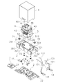
以下、図面を参照して実施形態にかかる逆流防止装置について説明する。図1は、逆流防止装置1の斜視図である。図2は、逆流防止装置1の上面図である。図3及び図4は、逆流防止装置1の分解斜視図である。図1から図4に示すように、逆流防止装置1は、ベース2と、端子台3と、接点機構部4と、電磁石ブロック5と、ケース6とを有する。
Hereinafter, a backflow prevention device according to an embodiment will be described with reference to the drawings. FIG. 1 is a perspective view of the
ベース2は、板状の形状を有しており、端子台3に取り付けられる。ベース2の一端には第1取付凸部21が設けられており、ベース2の他端には第2取付凸部22が設けられている。第1取付凸部21には、貫通孔211が設けられている。第2取付凸部22には、貫通孔221が設けられている。第1取付凸部21の貫通孔211と第2取付凸部22の貫通孔221とに図示しないネジが通されることによって、逆流防止装置1を所望の位置に取り付けることができる。
The
図4に示すように、ベース2の底面には、一対の係合溝201,202が設けられている。一対の係合溝201,202は、互いに間隔を空けて対向するように配置されている。係合溝201,202にスライドレール用保持具7が係合することで、スライドレール用保持具7がベース2に取り付けられる。
As shown in FIG. 4, a pair of
端子台3は、接点機構部4と電磁石ブロック5とケース6とを支持している。端子台3は、底面が開口した略箱状の形状を有する。平面視において、端子台3は、略長方形の形状を有する。端子台3は、端子台3の長手方向においてケース6より大きい。なお、本実施形態において特に説明がない限り「長手方向」は端子台3の長手方向を意味するものとする。
The
詳細には、端子台3は、第1側部31と第2側部32と端子台本体33とを有する。第1側部31と第2側部32と端子台本体33とは、長手方向に並んでいる。端子台本体33は、第1側部31と第2側部32との間に位置する。ケース6は、端子台本体33に取り付けられる。第1側部31は、ケース6から長手方向の一方に突出している。第2側部32は、ケース6から長手方向の他方に突出している。
Specifically, the
端子台3の底面の開口は、ベース2によって閉じられる。図3に示すように、端子台本体33の上面には、電磁石ブロック5を端子台3に取り付けるための第1取付部331と第2取付部332とが設けられている。第1取付部331と第2取付部332とは、端子台本体33の上面から突出している。
The opening at the bottom of the
第1側部31には、第1入力凹部311と第2入力凹部312とが設けられている。第1入力凹部311と第2入力凹部312とは、第1側部31の上面から下方に凹んだ形状を有する。第1入力凹部311の底面を貫通するように第1接続ネジ71が配置されており、第1接続ネジ71は、後述する入力端子11に螺合している。また、第2側部32には、第1出力凹部321と第2出力凹部322とが設けられている。第1出力凹部321と第2出力凹部322とは、第2側部32の上面から下方に凹んだ形状を有する。第1出力凹部321の底面を貫通するように第2接続ネジ72が配置されており、第2接続ネジ72は、後述する出力端子12に螺合している。これにより、端子台3に、出力端子12と入力端子11とが取り付けられる。
The
端子台3には、第1中継端子13とダイオード8とヒューズ9とが取り付けられる。第1中継端子13とダイオード8とヒューズ9とは、端子台3の内部に配置される。端子台3の内部の構造については後に詳細に説明する。
A
電磁石ブロック5は、端子台3上に配置される。電磁石ブロック5は、第1のネジ73と第2のネジ74とによって端子台3の第1取付部331と第2取付部332とに固定される。なお、本実施形態においては、端子台3に対して電磁石ブロック5が配置されている方向を上方と呼び、その反対の方向を下方と呼ぶ。接点機構部4は、電磁石ブロック5に取り付けられている。接点機構部4は、電磁石ブロック5の上方に配置されている。
The
ケース6は、底面が開口した略箱状の形状を有する。ケース6は、例えば透光性を有する樹脂によって形成される。ケース6の内部には、電磁石ブロック5と接点機構部4とが配置される。ケース6は、端子台3に取り付けられる。詳細には、ケース6の開口縁部の近傍には、係止孔601が設けられている。端子台3の側面には、係止突起301が設けられている。端子台3の係止突起301がケース6の係止孔601に係止することで、ケース6が端子台3に取り付けられる。また、端子台3の上面には、端子台3の短手方向に延びる第1溝部302と第2溝部303とが設けられている。ケース6が端子台3に取り付けられることで、ケース6の開口縁部は、第1溝部302内と第2溝部303内とに配置される。なお、本実施形態においては、特に説明が無い限り短手方向は、端子台3の短手方向を意味するものとする。
The
図5は、図2におけるV−V断面図である。図6は、図2におけるVI−VI断面図である。図5に示すように、電磁石ブロック5は、コイル51と、スプール52と、コア53と、ヨーク54とを有する。コイル51は、スプール52に巻回されている。コア53は、スプール52の中心孔に挿入されている。コア53は、鉄などの磁性材料で形成されている。コア53の一端は、ヨーク54に固定されている。コア53の他端には磁極部531が設けられている。磁極部531は、スプール52の一方の端部から突出している。磁極部531の外径は、スプール52の中心孔の内径よりも大きい。磁極部531は平坦な端面を有する。
5 is a cross-sectional view taken along the line VV in FIG. 6 is a cross-sectional view taken along the line VI-VI in FIG. As shown in FIG. 5, the
ヨーク54は、磁性材料で形成されている。ヨーク54は、屈曲した板状の形状を有する。詳細には、ヨーク54は、上面部541と側面部542と底面部543とを有する。上面部541と底面部543とは、側面部542によって接続されている。上述したコイル51は、上面部541と底面部543との間に配置される。コア53は、側面部542に固定される。
The
図6に示すように、接点機構部4は、可動接点部材41と固定接点部材42とを有する。可動接点部材41は、ヨーク54に対して揺動可能に支持されている。固定接点部材42は、ヨーク54に固定されている。可動接点部材41は、接極子43と、可動接触片44と、可動接触片支持部45と、を有する。接極子43は、磁性材料で形成されている。接極子43は、コア53の磁極部531と対向するように配置されている。可動接触片44は、ヨーク54の上方に配置される。可動接触片44は、導電性材料で形成されている。可動接触片44は、板状の形状を有する。可動接触片44の先端部には可動接点441が設けられている。
As shown in FIG. 6, the
可動接触片支持部45は、可動接触片44を支持している。可動接触片支持部45は、樹脂製であり、インサート成形により可動接触片44と一体化されている。接極子43の上部は、可動接触片支持部45に固定されている。接極子43の下部は、コア53の磁極部531と対向するように配置されている。接極子43は、ヨーク54に対して揺動可能に支持されている。図5に示すように、可動接触片支持部45には、復帰バネ46が取り付けられている。復帰バネ46は、接極子43が磁極部531から離れる方向に接極子43を付勢する。
The movable contact
固定接点部材42は、固定接触片47と、固定接触片支持部48と、支持台49とを有する。固定接触片47は、可動接触片44の上方に配置される。固定接触片47は、導電性材料で形成されている。固定接触片47は、板状の形状を有する。固定接触片47の先端部には固定接点471が設けられている。固定接点471は、可動接点441の上方に位置する。
The fixed
固定接触片支持部48は、固定接触片47を支持している。固定接触片支持部48は、樹脂製である。固定接触片47は、固定接触片支持部48の底面に取り付けられる。固定接触片支持部48には、第2中継端子14が取り付けられる。上述した復帰バネ46は、接極子43がコア53の磁極部531に接触した状態で、固定接触片支持部48の底面に押圧される。第2中継端子14は、図示しないリード線によって可動接触片44と接続される。第2中継端子14は、固定接触片支持部48の上面に取り付けられる。
The fixed contact
なお、図1に示すように、本実施形態に係る逆流防止装置1では、2つの固定接触片47と2つの第2中継端子14とが設けられている。図示を省略するが可動接触片44も2つ設けられている。すなわち、本実施形態に係る逆流防止装置1は、2組の固定接触片47と可動接触片44とを有している。
As shown in FIG. 1, in the
支持台49は、固定接触片支持部48の下方に配置される。支持台49は、可動接触片44の下方に配置される。支持台49は、ヨーク54の上方に配置される。支持台49は、絶縁シート40を介してヨーク54の上面に取り付けられる。図5に示すように、支持台49は、固定接触片支持部48と共にネジ75によってヨーク54に取り付けられる。支持台49の上面には、接点支持部491が取り付けられる。接点支持部491は、可動接点441の下方に位置している。接極子43が磁極部531から離れている状態で、可動接点441は、接点支持部491に接触する。
The
接点機構部4の動作は以下のとおりである。コイル51に流れる電流が所定の動作閾値未満であるときには、接極子43は、磁極部531から離れている状態である。このとき、可動接点441と固定接点471とは接触しておらず、電気的に遮断された状態である(遮断状態)。コイル51に動作閾値以上の電流が流れると、電磁石ブロック5が励磁されることで、復帰バネ46の付勢力に抗して接極子43が磁極部531に引き寄せられ、接極子43が磁極部531に接触する。このとき、可動接点441と固定接点471とが接触し、電気的に接続された状態となる(接続状態)。コイル51に流れる電流が、所定の復帰閾値以下になると、接極子43が復帰バネ46の付勢力によって磁極部531から離れる。これにより、可動接点441が固定接点471から離れることにより、接点機構部4は遮断状態に戻る。
The operation of the
次に、端子台3の内部の構成について詳細に説明する。図7は、端子台3の内部の構成を示す底面図である。図8及び図9は、端子台3の内部の構成を示す斜視図である。端子台3の内部には、入力端子11と、出力端子12と、第1中継端子13と、ヒューズ9と、接続部材10と、ダイオード8とが配置されている。
Next, the internal configuration of the
入力端子11は、端子台3の第1の角部313に配置される。出力端子12は、端子台3の第2の角部323に配置されている。第1の角部313は、第1側部31に設けられている。第2の角部323は、第2側部32に設けられている。第2の角部323は、第1の角部313の対角に位置する。従って、入力端子11と出力端子12とは、長手方向及び短手方向に間隔を空けて配置されている。
The
第1中継端子13は、出力端子12に隣接して配置されている。第1中継端子13は、端子台3の短手方向に出力端子12と並んでいる。第1中継端子13は、端子台3の短手方向における中央部に配置されている。
The
ヒューズ9は、入力端子11と出力端子12との間に配置される。ヒューズ9は、長手方向に沿って配置される。ヒューズ9は、長手方向において入力端子11と出力端子12との間、且つ、端子台3の短手方向において入力端子11と出力端子12との間に配置される。ヒューズ9は、長手方向における端子台3の中央部に配置されている。ヒューズ9は、端子台3の短手方向における端子台3の中央部に配置されている。ヒューズ9は、長手方向において第1中継端子13と並んで配置されている。
The
端子台3は、第1ボス部34と第2ボス部35とを有する。第1ボス部34には、上述した電磁石ブロック5を端子台3に固定するための第1のネジ73が配置される。第2ボス部35には、上述した電磁石ブロック5を端子台3に固定するための第2のネジ74が配置される。第1ボス部34と第2ボス部35とは、長手方向に間隔を空けて配置される。第1ボス部34と第2ボス部35とは、端子台3の短手方向に間隔を空けて配置される。
The
ヒューズ9は、第1ボス部34と第2ボス部35との間に配置される。ヒューズ9は、長手方向における第1ボス部34と第2ボス部35との間の距離よりも長い。長手方向において、ヒューズ9は、ダイオード8よりも長い。
The
ヒューズ9は、ヒューズ本体91と、第1リード線92と、第2リード線93と、を有する。ヒューズ本体91は、略筒状の形状を有する。ヒューズ本体91は、第1口金部94と、第2口金部95と、ガラス管部96と、を有する。第1口金部94は、長手方向において出力端子12よりも入力端子11に近い位置に配置される。第2口金部95は、長手方向において入力端子11よりも出力端子12に近い位置に配置される。ガラス管部96は、第1口金部94と第2口金部95との間に配置される。
The
第1リード線92と第2リード線93とは、ヒューズ本体91から突出している。第1リード線92は、第1口金部94からヒューズ本体91の軸線に垂直な方向に突出している。第2リード線93は、第2口金部95からヒューズ本体91の軸線に垂直な方向に突出している。第1リード線92と第2リード線93とは、ヒューズ本体91から同方向に突出している。詳細には、第1リード線92と第2リード線93とは、端子台3の短手方向において入力端子11側に向かってヒューズ本体91から突出している。
The
第1リード線92は、入力端子11に接続される。図10は、入力端子11の拡大図である。入力端子11は、端子本体111と接続部112とを有する。端子本体111は、板状の形状を有している。端子本体111には、上述した第1接続ネジ71が螺合するネジ孔113が設けられている。接続部112は、端子本体111から突出している。接続部112は、第1接続孔114と第2接続孔115と第3接続孔116とを有する。第1接続孔114と第2接続孔115とは、スリット117によって連結されている。スリット117は、接続部112の先端から接続部112の長手方向に延びている。第1接続孔114は、接続部112の先端と第2接続孔115との間に位置している。第3接続孔116は、スリット117と端子本体111との間に位置している。
The
図7に示すように、第1リード線92は、第1接続孔114に挿入されている。第1リード線92は、スリット117に圧入されることで、第1接続孔114に嵌合している。第1リード線92は、入力端子11の接続部112に半田付けされている。これにより、第1リード線92が入力端子11に接続されている。このように、ヒューズ9は、基板を介さずに入力端子11に接続されている。
As shown in FIG. 7, the
なお、出力端子12及び第1中継端子13は、入力端子11と同じ形状である。このため、図面においては、出力端子12の構成に対応する出力端子12及び第1中継端子13の構成に同じ符号を付している。
Note that the
接続部材10は、ヒューズ9とコイル51とを接続する。接続部材10は、細長い板状の形状を有する。接続部材10は、第1接続端部101と第2接続端部102とを有している。第1接続端部101にはスリット103が設けられている。上述したヒューズ9の第2リード線93は、第1接続端部101のスリット103に圧入されることで、第1接続端部101のスリット103に嵌合している。第2リード線93は、第1接続端部101に半田付けされている。これにより、第2リード線93が第1接続端部101に接続されている。このように、ヒューズ9は、基板を介さずに接続部材10に接続されている。
The
第2接続端部102にはスリット104が設けられている。図11は、端子台3の底面図である。図11に示すように、端子台3には、コイル51の第1の引出線511(図6参照)が通される貫通孔333が設けられている。図7に示すように、コイル51の第1の引出線511は、第2接続端部102のスリット104に圧入されることで第2接続端部102のスリット104に嵌合している。第1の引出線511は、第2接続端部102に半田付けされている。これにより、第1の引出線511が第2接続端部102に接続されている。
The
第1接続端部101と第2接続端部102とは、ヒューズ9を間に挟んで互いに反対側に配置されている。従って、底面視において、接続部材10は、ヒューズ9と交差するように配置される。詳細には、第1接続端部101は、ヒューズ本体91に対して第1リード線92及び第2リード線93が突出している方向に位置している。第2接続端部102は、ヒューズ本体91に対して第1リード線92及び第2リード線93が突出している方向と反対の方向に位置している。
The first
第1接続端部101は、長手方向において、入力端子11よりも出力端子12に近い位置に配置される。第1接続端部101は、端子台3の短手方向において、出力端子12よりも入力端子11に近い位置に配置される。第2接続端部102は、長手方向において、出力端子12よりも入力端子11に近い位置に配置される。第2接続端部102は、端子台3の短手方向において、入力端子11よりも出力端子12に近い位置に配置される。
The first
接続部材10は、底面視において第2口金部95と交差するように配置される。第2口金部95から突出する第2リード線93は、第1接続端部101において接続部材10に接続されている。従って、接続部材10は、底面視において接続部材10と同極である第2口金部95と交差するように配置される。また、接続部材10は、底面視において第1ボス部34と第2ボス部35との間を通るように配置される。図9に示すように、接続部材10は、ヒューズ9を乗り越えるように上下方向に屈曲した形状を有している。
The connecting
図11に示すように、端子台3には、コイル51の第2の引出線512が通される貫通孔334が設けられている。コイル51の第2の引出線512は、第1中継端子13の第2接続孔115に挿入されている。第2の引出線512は、第1中継端子13に半田付けされている。これにより、第2の引出線512が第1中継端子13に接続されている。
As shown in FIG. 11, the
第1中継端子13には、中継リード線131が接続されている。図11に示すように、端子台3には、中継リード線131が通される貫通孔335が設けられている。中継リード線131は、第1中継端子13の第3接続孔116に挿入されている。中継リード線131は、第1中継端子13に半田付けされている。これにより、第2の引出線512が第1中継端子13に接続されている。中継リード線131は、上述した第2中継端子14に接続されている。
A
図1に示すように、上述した固定接触片47には、出力リード線121が接続されている。図11に示すように、端子台3には、出力リード線121が通される貫通孔336が設けられている。出力リード線121は、出力端子12の第2接続孔115に挿入されている。出力リード線121は、出力端子12に半田付けされている。これにより、出力リード線121が出力端子12に接続されている。
As shown in FIG. 1, the
また、第1中継端子13と出力端子12とには、ダイオード8が接続されている。ダイオード8は、ダイオード本体81と第1ダイオードリード線82と第2ダイオードリード線83とを有する。第1ダイオードリード線82は、ダイオード本体81の軸線方向の一方にダイオード本体81から突出している。第2ダイオードリード線83は、ダイオード本体81の軸線方向の他方にダイオード本体81から突出している。
A
第1ダイオードリード線82は、第1中継端子13のスリット117に圧入されることで、第1中継端子13の第1接続孔114に嵌合している。第1ダイオードリード線82は、第1中継端子13に半田付けされている。これにより、第1ダイオードリード線82が第1中継端子13の第1接続孔114に接続されている。第2ダイオードリード線83は、出力端子12のスリット117に圧入されることで、出力端子12の第1接続孔114に嵌合している。第2ダイオードリード線83は、出力端子12に半田付けされている。これにより、第2ダイオードリード線83が出力端子12の第1接続孔114に接続されている。
The
ダイオード8は、長手方向においてヒューズ9と出力端子12との間、且つ、短手方向においてヒューズ9と出力端子12との間に配置される。ダイオード8は、短手方向において第1中継端子13と出力端子12との間に配置される。ダイオード8は、長手方向において第2ボス部35と出力端子12との間に配置される。なお、図11に示すように、端子台3には、ダイオード8を支持するダイオード支持リブ309が設けられている。
The
図11に示すように、端子台3は、第1横支持リブ304と第2横支持リブ305と第3横支持リブ306とを有する。第1横支持リブ304と第2横支持リブ305と第3横支持リブ306とは、ヒューズ9に対向するように配置される。第1横支持リブ304と第2横支持リブ305と第3横支持リブ306とは、ヒューズ9の側方からヒューズ9を支持する。
As shown in FIG. 11, the
第1横支持リブ304と第2横支持リブ305とは、互いに対向するように配置される。ヒューズ9は、第1横支持リブ304と第2横支持リブ305との間に配置される。詳細には、第1口金部94が、第1横支持リブ304と第2横支持リブ305との間に配置される。
The first
第3横支持リブ306は、第2ボス部35に対向するように配置される。ヒューズ9は、第3横支持リブ306と第2ボス部35との間に配置される。詳細には、第2口金部95が第3横支持リブ306と第2ボス部35との間に配置される。
The third
端子台3は、第1上支持リブ307と第2上支持リブ308とを有する。第1上支持リブ307は、ヒューズ9の一側方に位置している。第2上支持リブ308は、ヒューズ9の他側方に位置している。第1上支持リブ307と第2上支持リブ308とは、接続部材10に対向するように配置されている。第1上支持リブ307と第2上支持リブ308とは、接続部材10の上方において接続部材10を支持する。
The
図12は、ベース2の上面図である。図12においては、ヒューズ9及び接続部材10の位置を二点鎖線で示している。図12に示すように、ベース2は、第1下ヒューズ支持リブ203と第2下ヒューズ支持リブ204とを有する。第1下ヒューズ支持リブ203は、第1口金部94の下方に位置する。第1下ヒューズ支持リブ203は、第1口金部94に対向するように配置されている。第1下ヒューズ支持リブ203は、第1口金部94を支持する。第2下ヒューズ支持リブ204は、第2口金部95の下方に位置する。第2下ヒューズ支持リブ204は、第2口金部95に対向するように配置されている。第2下ヒューズ支持リブ204は、第2口金部95を支持する。
FIG. 12 is a top view of the
ベース2は、第1下支持リブ205と第2下支持リブ206とを有する。第1下支持リブ205は、第1上支持リブ307の下方に位置する。第2下支持リブ206は、第2上支持リブ308の下方に位置する。第1下支持リブ205と第2下支持リブ206とは、接続部材10の下方において接続部材10を支持する。
The
ベース2は、第1ボスカバー部207と第2ボスカバー部208とを有する。第1ボスカバー部207は、第1ボス部34の下方に位置する。第1ボスカバー部207は、第1ボス部34を下方から覆う。第2ボスカバー部208は、第2ボス部35の下方に位置する。第2ボスカバー部208は、第2ボス部35を下方から覆う。
The
ヒューズ9は、第1ボスカバー部207と第2ボスカバー部208との間に配置されている。また、接続部材10は、第1ボスカバー部207と第2ボスカバー部208との間を通るように配置されている。
The
図13は、本実施形態に係る逆流防止装置1が採用された太陽光発電システム100の構成を示す模式図である。太陽光発電システム100は、太陽電池200と蓄電池300と逆流防止装置1とを備えている。太陽電池200は、逆流防止装置1の入力端子11に接続される。蓄電池300は、逆流防止装置1の出力端子12に接続される。また、上述した逆流防止装置1の構成により、図13に示すように、入力端子11と出力端子12とを接続する回路15が構成されている。
FIG. 13 is a schematic diagram illustrating a configuration of a solar
この回路15において入力端子11と出力端子12との間にはダイオード8が配置される。ダイオード8は、入力端子11から出力端子12への電流の流れを許容し、出力端子12から入力端子11への電流の流れを規制する。入力端子11とダイオード8とに直列に、コイル51が配置される。接点機構部4は、ダイオード8に並列に接続される。ヒューズ9は、入力端子11とコイル51との間に配置され、ダイオード8に直列に接続される。なお、図13ではコイル51が入力端子11とダイオード8との間に配置されているが、コイル51がダイオード8と出力端子12との間に配置されてもよい。
In this
図14は、太陽光発電システム100における逆流防止装置1の動作を示すタイミングチャートである。図14(A)は、逆流防止装置1に流れる電流値の変化を示している。図14(B)は、逆流防止装置1における接点機構部4の状態の変化を示している。
FIG. 14 is a timing chart showing the operation of the
太陽光発電システム100において、太陽電池200が発電すると、入力端子11を介してコイル51へ電流が流れる。太陽光が弱く、コイル51に流れる電流値が所定の動作閾値I_th1(例えば、3A)未満であるときには(時点t0から時点t1)、電磁石ブロック5は励磁しない。このため、接点機構部4は、遮断状態(OFF)に維持される。従って、太陽電池200から供給された電流は、ダイオード8を介して蓄電池300に充電される。また、太陽電池200の発電量が小さく、蓄電池300の電圧が太陽電池200の電圧に勝った場合、蓄電池300から太陽電池200へと電流が逆流しようとするが、接点機構部4が遮断状態となっているため、ダイオード8によって電流の逆流が阻止される。これにより、太陽電池200に逆電流が流れ込むことを防止することができ、太陽電池200の損傷を防止することができる。
In the solar
一方、太陽光が強く、コイル51に流れる電流値が動作閾値I_th1以上になると(時点t1)、電磁石ブロック5が励磁し、接点機構部4が、遮断状態(OFF)から接続状態(ON)に切り換わる。従って、太陽電池200から供給された電流は、ダイオード8を迂回し、電気抵抗値の少ない接点機構部4を介して蓄電池300に充電される。このため、太陽電池200での発電量が大きい場合、ダイオード8に大電流が流れることはない。従って、ダイオード8でのエネルギーロス、或いは、ダイオード8の損傷などの不具合の発生を抑えることができる。
On the other hand, when sunlight is strong and the current value flowing through the
なお、コイル51に流れる電流値が所定の復帰閾値I_th2以上であるときには(時点t1から時点t2)、接点機構部4は、接続状態(ON)に維持される。そして、電流値が復帰閾値I_th2未満になると(時点t2)、接点機構部4は、接続状態(ON)から遮断状態(OFF)に切り換えられる。
Note that when the value of the current flowing through the
上述したように本実施形態に係る逆流防止装置1では、地絡、或いは、太陽電池200のパネル間の短絡などの要因により、回路15に過電流が流れると、ヒューズ9が切れることで、回路15が保護される。すなわち、ヒューズ9によって過電流に対する保護回路が構成されている。このため、過電流が回路15に流れたときに、ダイオード8或いは接点機構部4が損傷することを防止することができる。また、過電流が回路15に流れたときに、逆流防止装置1をオープン故障させることで、逆流防止装置1が搭載されたシステム100を保護することができる。
As described above, in the
ヒューズ9は、端子台3の内部に収容されており、長手方向に沿って配置されている。また、ヒューズ9は、長手方向において入力端子11と出力端子12との間、且つ、端子台3の短手方向において入力端子11と出力端子12との間に配置される。このため、ヒューズ9を端子台3にコンパクトに収容することができる。さらに、ダイオード8は、長手方向においてヒューズ9と出力端子12との間、且つ、端子台3の短手方向においてヒューズ9と出力端子12との間に配置される。このため、ヒューズ9とダイオード8とを端子台3にコンパクトに収容することができる。
The
ヒューズ9とコイル51とを接続する接続部材10が、ヒューズ9と交差するように配置される。このため、ヒューズ9からのリード線92,93の突出方向、或いは、入力端子11と出力端子12との位置関係に関らずに、ヒューズ9を端子台3内に配置することができる。これにより、端子台3の内部に配置される部品のレイアウトの自由度を向上させることができる。
A connecting
接続部材10は、第2口金部95と交差するように配置される。このため、強度の低いガラス管部96を接続部材10から保護することができる。また、第2口金部95は接続部材10と同極であるため、接続部材10が第2口金部95と接触しても、短絡を防止することができる。
The connecting
接続部材10は、板状の形状を有する。このため、接続部材10の放熱効果を向上させることができる。
The connecting
第2リード線93は、接続部材10のスリット103に嵌合している。このため、第2リード線93と接続部材10とを固定している半田付け部分が発熱によって溶融しても、ヒューズ9が接続部材10から外れることが抑えられる。
The
ヒューズ9は、基板を介さずに、第1リード線92を介して入力端子11に接続される。また、ヒューズ9は、基板を介さずに、接続部材10を介してコイル51に接続される。このため、ヒューズ9が基板に実装される場合と比べて、基板の厚さ、銅箔の厚さ、或いは、パターン幅などの基板の設計における制限によらず、放熱効果を向上させることができる。
The
端子台3は、ヒューズ9を支持する第1横支持リブ304と第2横支持リブ305と第3横支持リブ306とを有する。また、ベース2は、第1下ヒューズ支持リブ203と第2下ヒューズ支持リブ204とを有している。このため、端子台3の内部においてヒューズ9が移動することを、これらのリブによって抑えることができる。従って、本実施形態のようにヒューズ9が基板を介さずに回路15に接続されていても、ヒューズ9の移動をこれらのリブによって規制することができる。特に、第1横支持リブ304と第2横支持リブ305と第3横支持リブ306とによってヒューズ9の横方向への移動を規制することができる。また、第1下ヒューズ支持リブ203と第2下ヒューズ支持リブ204とによって、ヒューズ9の上下方向への移動を規制することができる。
The
端子台3は、接続部材10を支持する第1上支持リブ307と第2上支持リブ308とを有する。また、ベース2は、第1下支持リブ205と第2下支持リブ206とを有する。このため、端子台3の内部において接続部材10の上下方向への揺れをこれらのリブによって抑えることができる。特に、本実施形態のように、接続部材10がヒューズ9に交差するように配置されることで、接続部材10の長さが大きくなっても、接続部材10の揺れを抑えることで、端子台3内の他の部材との接触を抑えることができる。
The
以上、本発明の一実施形態について説明したが、本発明は上記実施形態に限定されるものではなく、発明の要旨を逸脱しない範囲で種々の変更が可能である。 As mentioned above, although one Embodiment of this invention was described, this invention is not limited to the said embodiment, A various change is possible in the range which does not deviate from the summary of invention.
入力端子11、中継端子、出力端子12、ダイオード8、及び、ヒューズ9は、上述した実施形態の位置及び形状に限らず、変更されてもよい。例えば、図15に示すように、ヒューズ9は、回路15においてダイオード8と出力端子12との間に配置されてもよい。
The
接続部材10は、上述した実施形態の位置及び形状に限られず、変更されてもよい。例えば、接続部材10がヒューズ9と交差しないように配置されてもよい。接続部材10は、板状の形状に限らず、線状であってもよい。
The connecting
接点機構部4及び電磁石ブロック5は、上述した実施形態の構成に限らず、変更されてもよい。例えば、上記の実施形態では、可動接点441と固定接点471との組の数は2つであるが、1つ或いは3つ以上であってもよい。
The
端子台3は、上記の実施形態の形状に限られず、変更されてもよい。例えば、端子台3が、底面視において略正方形であってもよい。或いは、端子台3が、底面視において四角形以外の形状であってもよい。端子台3のリブが省略されてもよい。同様に、ベース2のリブが省略されてもよい。
The
本発明によれば、過電流による逆流防止装置の損傷を防止することができる。 ADVANTAGE OF THE INVENTION According to this invention, the damage of the backflow prevention apparatus by overcurrent can be prevented.
11 入力端子
12 出力端子
15 回路
8 ダイオード
51 コイル
4 接点機構部
9 ヒューズ
1 逆流防止装置
3 端子台
10 接続部材
94 第1口金部
95 第2口金部
96 ガラス管部
91 ヒューズ本体
92 第1リード線
93 第2リード線
304 第1横支持リブ
305 第2横支持リブ
306 第3横支持リブ
307 第1上支持リブ
308 第2上支持リブ
DESCRIPTION OF
Claims (10)
出力端子と、 An output terminal;
前記入力端子と前記出力端子とを接続する回路と、 A circuit for connecting the input terminal and the output terminal;
前記回路において前記入力端子と前記出力端子との間に配置され、前記入力端子から前記出力端子への電流の流れを許容し、前記出力端子から前記入力端子への電流の流れを規制するダイオードと、 A diode disposed between the input terminal and the output terminal in the circuit, allowing a current flow from the input terminal to the output terminal, and restricting a current flow from the output terminal to the input terminal; ,
前記回路において前記入力端子と前記ダイオードとに直列に配置されるコイルと、 A coil disposed in series with the input terminal and the diode in the circuit;
前記回路において前記ダイオードに並列に接続され、前記コイルに流れる電流が所定の動作閾値未満であるときには遮断状態を維持し、前記コイルに前記動作閾値以上の電流が流れることで接続状態となる接点機構部と、 A contact mechanism that is connected in parallel to the diode in the circuit, maintains a shut-off state when a current flowing through the coil is less than a predetermined operating threshold value, and enters a connected state when a current greater than the operating threshold value flows through the coil. And
前記回路において前記ダイオードに直列に接続されるヒューズと、 A fuse connected in series with the diode in the circuit;
前記コイルと前記接点機構部とを支持し、前記入力端子と前記出力端子とが取り付けられる端子台と、 A terminal block that supports the coil and the contact mechanism, and to which the input terminal and the output terminal are attached;
前記ヒューズと前記コイルとを接続する接続部材と、 A connecting member for connecting the fuse and the coil;
を備え、With
前記ヒューズは、前記端子台の内部に収容され、 The fuse is housed inside the terminal block;
前記ヒューズは、一対の口金部と、前記一対の口金部の間に配置されるガラス管部と、を有し、 The fuse has a pair of base parts, and a glass tube part disposed between the pair of base parts,
前記接続部材は、前記一対の口金部の一方と交差するように配置される、 The connecting member is disposed so as to intersect with one of the pair of base parts.
逆流防止装置。Backflow prevention device.
前記出力端子は、前記端子台の他方の端部に配置され、
前記ヒューズは、前記入力端子と前記出力端子との間に配置される、
請求項1に記載の逆流防止装置。 The input terminal is disposed at one end of the terminal block,
The output terminal is disposed at the other end of the terminal block;
The fuse is disposed between the input terminal and the output terminal;
The backflow prevention device according to claim 1.
請求項1又は2に記載の逆流防止装置。 The fuse is disposed along a longitudinal direction of the terminal block;
The backflow prevention device according to claim 1 or 2.
前記入力端子は、前記端子台の第1の角部に配置され、
前記出力端子は、前記端子台の前記第1の角部の対角に位置する第2の角部に配置され、
前記ヒューズは、前記端子台の長手方向に沿って配置され、
前記ヒューズは、前記端子台の長手方向において前記入力端子と前記出力端子との間、且つ、前記端子台の短手方向において前記入力端子と前記出力端子との間に配置され、
前記ダイオードは、前記端子台の長手方向において前記ヒューズと前記出力端子との間、且つ、前記端子台の短手方向において前記ヒューズと前記出力端子との間に配置される、
請求項1に記載の逆流防止装置。 The fuse and the diode are housed inside the terminal block,
The input terminal is disposed at a first corner of the terminal block;
The output terminal is disposed at a second corner portion located diagonally to the first corner portion of the terminal block,
The fuse is disposed along the longitudinal direction of the terminal block,
The fuse is disposed between the input terminal and the output terminal in the longitudinal direction of the terminal block, and between the input terminal and the output terminal in the short direction of the terminal block,
The diode is disposed between the fuse and the output terminal in the longitudinal direction of the terminal block, and between the fuse and the output terminal in the short direction of the terminal block.
The backflow prevention device according to claim 1.
請求項1から4のいずれかに記載の逆流防止装置。 The connection member is arranged so as to intersect the base part having the same polarity as the connection member among the pair of base parts.
The backflow prevention device according to any one of claims 1 to 4 .
請求項1から5のいずれかに記載の逆流防止装置。 The connecting member has a plate shape,
The backflow prevention device according to any one of claims 1 to 5 .
前記リード線は、前記接続部材に半田付けされており、
前記接続部材は、前記リード線が嵌合されるスリットを有する、
請求項1から6のいずれかに記載の逆流防止装置。 The fuse has a fuse body and a lead wire protruding from the fuse body,
The lead wire is soldered to the connection member,
The connection member has a slit into which the lead wire is fitted.
The backflow prevention device according to any one of claims 1 to 6 .
請求項7に記載の逆流防止装置。 The fuse is connected to the input terminal or the output terminal via the lead wire without going through a substrate.
The backflow prevention device according to claim 7 .
請求項1から8のいずれかに記載の逆流防止装置。 The terminal block has a rib disposed so as to face the connection member.
The backflow prevention device according to any one of claims 1 to 8 .
請求項1から9のいずれかに記載の逆流防止装置。 The terminal block has a rib arranged to face the fuse.
The backflow prevention device according to any one of claims 1 to 9 .
Priority Applications (4)
| Application Number | Priority Date | Filing Date | Title |
|---|---|---|---|
| JP2013248253A JP6287128B2 (en) | 2013-11-29 | 2013-11-29 | Backflow prevention device |
| KR1020140162563A KR20150062958A (en) | 2013-11-29 | 2014-11-20 | Backdraft prevention device |
| CN201410691527.3A CN104682373B (en) | 2013-11-29 | 2014-11-25 | Anti-backflow device |
| KR1020160156412A KR20160137904A (en) | 2013-11-29 | 2016-11-23 | Backdraft prevention device |
Applications Claiming Priority (1)
| Application Number | Priority Date | Filing Date | Title |
|---|---|---|---|
| JP2013248253A JP6287128B2 (en) | 2013-11-29 | 2013-11-29 | Backflow prevention device |
Publications (2)
| Publication Number | Publication Date |
|---|---|
| JP2015106989A JP2015106989A (en) | 2015-06-08 |
| JP6287128B2 true JP6287128B2 (en) | 2018-03-07 |
Family
ID=53317111
Family Applications (1)
| Application Number | Title | Priority Date | Filing Date |
|---|---|---|---|
| JP2013248253A Active JP6287128B2 (en) | 2013-11-29 | 2013-11-29 | Backflow prevention device |
Country Status (3)
| Country | Link |
|---|---|
| JP (1) | JP6287128B2 (en) |
| KR (2) | KR20150062958A (en) |
| CN (1) | CN104682373B (en) |
Family Cites Families (11)
| Publication number | Priority date | Publication date | Assignee | Title |
|---|---|---|---|---|
| JPS5321403Y2 (en) * | 1973-06-01 | 1978-06-05 | ||
| JPS54181272U (en) * | 1978-06-13 | 1979-12-21 | ||
| JPH02126380U (en) * | 1989-03-27 | 1990-10-18 | ||
| JP3289394B2 (en) * | 1992-06-19 | 2002-06-04 | オムロン株式会社 | Backflow prevention device and solar cell protection device |
| JP3325299B2 (en) * | 1992-09-10 | 2002-09-17 | 株式会社ソキア | Power supply |
| JPH10106658A (en) * | 1996-09-30 | 1998-04-24 | Morimatsu:Kk | Easy-to-demount terminal block with built-in fuse |
| JP2007325413A (en) * | 2006-06-01 | 2007-12-13 | Nippon Telegr & Teleph Corp <Ntt> | Current divider |
| US8723031B2 (en) * | 2010-08-30 | 2014-05-13 | Hosiden Corporation | Terminal box |
| JP6024194B2 (en) * | 2012-05-15 | 2016-11-09 | オムロン株式会社 | Relay unit and manufacturing method thereof |
| JP5831408B2 (en) * | 2012-09-11 | 2015-12-09 | 株式会社オートネットワーク技術研究所 | Electrical junction box |
| CN202898223U (en) * | 2012-10-12 | 2013-04-24 | 好利来(中国)电子科技股份有限公司 | Fuse with glass tube with frosted outer circumferential surface at end |
-
2013
- 2013-11-29 JP JP2013248253A patent/JP6287128B2/en active Active
-
2014
- 2014-11-20 KR KR1020140162563A patent/KR20150062958A/en active Application Filing
- 2014-11-25 CN CN201410691527.3A patent/CN104682373B/en active Active
-
2016
- 2016-11-23 KR KR1020160156412A patent/KR20160137904A/en not_active Application Discontinuation
Also Published As
| Publication number | Publication date |
|---|---|
| CN104682373B (en) | 2017-11-17 |
| CN104682373A (en) | 2015-06-03 |
| KR20150062958A (en) | 2015-06-08 |
| KR20160137904A (en) | 2016-12-01 |
| JP2015106989A (en) | 2015-06-08 |
Similar Documents
| Publication | Publication Date | Title |
|---|---|---|
| US8841979B2 (en) | Relay | |
| US20110121926A1 (en) | Electromagnetic relay | |
| US20130033344A1 (en) | Electromagnetic relay | |
| JP7026327B2 (en) | Contact devices, electromagnetic relays and electrical equipment | |
| US9196433B2 (en) | Electromagnetic switch | |
| JP2009158221A (en) | Electromagnetic switch device | |
| JP6287128B2 (en) | Backflow prevention device | |
| JP2016071937A (en) | Battery terminal | |
| JP2011070900A (en) | Fusible link unit | |
| JP2020080256A (en) | Contact device and electromagnetic relay | |
| US20150102895A1 (en) | Fuse, fuse box, and fuse device | |
| JP2017004874A (en) | Terminal block | |
| JP6051703B2 (en) | Backflow prevention device and photovoltaic power generation system provided with the same | |
| JP6175256B2 (en) | fuse | |
| JP2017098194A (en) | Dc switch device | |
| WO2017073539A1 (en) | Fuse element | |
| JP2013125635A (en) | Circuit breaker | |
| JP2010062078A (en) | Electromagnetic contactor | |
| JP7076635B2 (en) | Circuit breaker | |
| JP5922426B2 (en) | Circuit breaker | |
| JP2003087940A (en) | Electric junction box | |
| JP4091012B2 (en) | Circuit breaker | |
| JP5908300B2 (en) | Circuit breaker | |
| JP5189919B2 (en) | fuse | |
| JP2014053201A5 (en) |
Legal Events
| Date | Code | Title | Description |
|---|---|---|---|
| A621 | Written request for application examination |
Free format text: JAPANESE INTERMEDIATE CODE: A621 Effective date: 20161005 |
|
| A977 | Report on retrieval |
Free format text: JAPANESE INTERMEDIATE CODE: A971007 Effective date: 20170623 |
|
| A131 | Notification of reasons for refusal |
Free format text: JAPANESE INTERMEDIATE CODE: A131 Effective date: 20170704 |
|
| A521 | Written amendment |
Free format text: JAPANESE INTERMEDIATE CODE: A523 Effective date: 20170901 |
|
| RD03 | Notification of appointment of power of attorney |
Free format text: JAPANESE INTERMEDIATE CODE: A7423 Effective date: 20170901 |
|
| RD04 | Notification of resignation of power of attorney |
Free format text: JAPANESE INTERMEDIATE CODE: A7424 Effective date: 20170901 |
|
| A131 | Notification of reasons for refusal |
Free format text: JAPANESE INTERMEDIATE CODE: A131 Effective date: 20171031 |
|
| A521 | Written amendment |
Free format text: JAPANESE INTERMEDIATE CODE: A523 Effective date: 20171218 |
|
| TRDD | Decision of grant or rejection written | ||
| A01 | Written decision to grant a patent or to grant a registration (utility model) |
Free format text: JAPANESE INTERMEDIATE CODE: A01 Effective date: 20180109 |
|
| A61 | First payment of annual fees (during grant procedure) |
Free format text: JAPANESE INTERMEDIATE CODE: A61 Effective date: 20180122 |
|
| R150 | Certificate of patent or registration of utility model |
Ref document number: 6287128 Country of ref document: JP Free format text: JAPANESE INTERMEDIATE CODE: R150 |