JP6286780B2 - Electronic devices for radio frequency or power applications and processes for manufacturing such devices - Google Patents
Electronic devices for radio frequency or power applications and processes for manufacturing such devices Download PDFInfo
- Publication number
- JP6286780B2 JP6286780B2 JP2016159361A JP2016159361A JP6286780B2 JP 6286780 B2 JP6286780 B2 JP 6286780B2 JP 2016159361 A JP2016159361 A JP 2016159361A JP 2016159361 A JP2016159361 A JP 2016159361A JP 6286780 B2 JP6286780 B2 JP 6286780B2
- Authority
- JP
- Japan
- Prior art keywords
- layer
- substrate
- support substrate
- silicon
- manufacturing
- Prior art date
- Legal status (The legal status is an assumption and is not a legal conclusion. Google has not performed a legal analysis and makes no representation as to the accuracy of the status listed.)
- Active
Links
- 238000000034 method Methods 0.000 title claims description 56
- 230000008569 process Effects 0.000 title claims description 47
- 238000004519 manufacturing process Methods 0.000 title claims description 29
- 239000000758 substrate Substances 0.000 claims description 181
- 239000010410 layer Substances 0.000 claims description 150
- 239000004065 semiconductor Substances 0.000 claims description 40
- 239000002344 surface layer Substances 0.000 claims description 32
- XUIMIQQOPSSXEZ-UHFFFAOYSA-N Silicon Chemical compound [Si] XUIMIQQOPSSXEZ-UHFFFAOYSA-N 0.000 claims description 31
- 229910052710 silicon Inorganic materials 0.000 claims description 31
- 239000010703 silicon Substances 0.000 claims description 31
- PCHJSUWPFVWCPO-UHFFFAOYSA-N gold Chemical compound [Au] PCHJSUWPFVWCPO-UHFFFAOYSA-N 0.000 claims description 9
- 239000010931 gold Substances 0.000 claims description 8
- 229910052737 gold Inorganic materials 0.000 claims description 8
- 230000003647 oxidation Effects 0.000 claims 1
- 238000007254 oxidation reaction Methods 0.000 claims 1
- 239000000463 material Substances 0.000 description 24
- VYPSYNLAJGMNEJ-UHFFFAOYSA-N Silicium dioxide Chemical compound O=[Si]=O VYPSYNLAJGMNEJ-UHFFFAOYSA-N 0.000 description 12
- 229910052814 silicon oxide Inorganic materials 0.000 description 12
- 235000012431 wafers Nutrition 0.000 description 11
- PNEYBMLMFCGWSK-UHFFFAOYSA-N aluminium oxide Inorganic materials [O-2].[O-2].[O-2].[Al+3].[Al+3] PNEYBMLMFCGWSK-UHFFFAOYSA-N 0.000 description 10
- OKTJSMMVPCPJKN-UHFFFAOYSA-N Carbon Chemical compound [C] OKTJSMMVPCPJKN-UHFFFAOYSA-N 0.000 description 7
- 229910052799 carbon Inorganic materials 0.000 description 7
- 229910052594 sapphire Inorganic materials 0.000 description 7
- 239000010980 sapphire Substances 0.000 description 7
- 230000015572 biosynthetic process Effects 0.000 description 6
- 229910052782 aluminium Inorganic materials 0.000 description 4
- XAGFODPZIPBFFR-UHFFFAOYSA-N aluminium Chemical compound [Al] XAGFODPZIPBFFR-UHFFFAOYSA-N 0.000 description 4
- 230000004888 barrier function Effects 0.000 description 4
- 239000011248 coating agent Substances 0.000 description 4
- 238000000576 coating method Methods 0.000 description 4
- 229910021420 polycrystalline silicon Inorganic materials 0.000 description 4
- 229910000756 V alloy Inorganic materials 0.000 description 3
- 238000005229 chemical vapour deposition Methods 0.000 description 3
- 238000000151 deposition Methods 0.000 description 3
- 238000005530 etching Methods 0.000 description 3
- 229910052732 germanium Inorganic materials 0.000 description 3
- GNPVGFCGXDBREM-UHFFFAOYSA-N germanium atom Chemical compound [Ge] GNPVGFCGXDBREM-UHFFFAOYSA-N 0.000 description 3
- 230000017525 heat dissipation Effects 0.000 description 3
- 238000010438 heat treatment Methods 0.000 description 3
- 239000012212 insulator Substances 0.000 description 3
- JBRZTFJDHDCESZ-UHFFFAOYSA-N AsGa Chemical compound [As]#[Ga] JBRZTFJDHDCESZ-UHFFFAOYSA-N 0.000 description 2
- 229910017214 AsGa Inorganic materials 0.000 description 2
- 229910002601 GaN Inorganic materials 0.000 description 2
- JMASRVWKEDWRBT-UHFFFAOYSA-N Gallium nitride Chemical compound [Ga]#N JMASRVWKEDWRBT-UHFFFAOYSA-N 0.000 description 2
- 238000000407 epitaxy Methods 0.000 description 2
- 150000004767 nitrides Chemical class 0.000 description 2
- 238000000623 plasma-assisted chemical vapour deposition Methods 0.000 description 2
- 230000035882 stress Effects 0.000 description 2
- 239000000126 substance Substances 0.000 description 2
- 238000004381 surface treatment Methods 0.000 description 2
- 230000008646 thermal stress Effects 0.000 description 2
- 229910004298 SiO 2 Inorganic materials 0.000 description 1
- 238000007743 anodising Methods 0.000 description 1
- 238000003486 chemical etching Methods 0.000 description 1
- 238000005520 cutting process Methods 0.000 description 1
- 230000008021 deposition Effects 0.000 description 1
- 238000009792 diffusion process Methods 0.000 description 1
- 230000000694 effects Effects 0.000 description 1
- 238000003487 electrochemical reaction Methods 0.000 description 1
- 239000003792 electrolyte Substances 0.000 description 1
- 238000005538 encapsulation Methods 0.000 description 1
- 230000001747 exhibiting effect Effects 0.000 description 1
- 230000006872 improvement Effects 0.000 description 1
- 238000009413 insulation Methods 0.000 description 1
- 230000003993 interaction Effects 0.000 description 1
- 238000004377 microelectronic Methods 0.000 description 1
- 230000000877 morphologic effect Effects 0.000 description 1
- 238000005121 nitriding Methods 0.000 description 1
- 230000003071 parasitic effect Effects 0.000 description 1
- 230000035515 penetration Effects 0.000 description 1
- 238000005498 polishing Methods 0.000 description 1
- 230000009467 reduction Effects 0.000 description 1
- 238000000926 separation method Methods 0.000 description 1
- 239000007787 solid Substances 0.000 description 1
- 238000004544 sputter deposition Methods 0.000 description 1
- 239000002470 thermal conductor Substances 0.000 description 1
Images


Classifications
-
- H—ELECTRICITY
- H01—ELECTRIC ELEMENTS
- H01L—SEMICONDUCTOR DEVICES NOT COVERED BY CLASS H10
- H01L21/00—Processes or apparatus adapted for the manufacture or treatment of semiconductor or solid state devices or of parts thereof
- H01L21/70—Manufacture or treatment of devices consisting of a plurality of solid state components formed in or on a common substrate or of parts thereof; Manufacture of integrated circuit devices or of parts thereof
- H01L21/71—Manufacture of specific parts of devices defined in group H01L21/70
- H01L21/76—Making of isolation regions between components
- H01L21/762—Dielectric regions, e.g. EPIC dielectric isolation, LOCOS; Trench refilling techniques, SOI technology, use of channel stoppers
-
- H—ELECTRICITY
- H05—ELECTRIC TECHNIQUES NOT OTHERWISE PROVIDED FOR
- H05K—PRINTED CIRCUITS; CASINGS OR CONSTRUCTIONAL DETAILS OF ELECTRIC APPARATUS; MANUFACTURE OF ASSEMBLAGES OF ELECTRICAL COMPONENTS
- H05K1/00—Printed circuits
- H05K1/18—Printed circuits structurally associated with non-printed electric components
-
- H—ELECTRICITY
- H01—ELECTRIC ELEMENTS
- H01L—SEMICONDUCTOR DEVICES NOT COVERED BY CLASS H10
- H01L21/00—Processes or apparatus adapted for the manufacture or treatment of semiconductor or solid state devices or of parts thereof
- H01L21/02—Manufacture or treatment of semiconductor devices or of parts thereof
- H01L21/04—Manufacture or treatment of semiconductor devices or of parts thereof the devices having potential barriers, e.g. a PN junction, depletion layer or carrier concentration layer
- H01L21/18—Manufacture or treatment of semiconductor devices or of parts thereof the devices having potential barriers, e.g. a PN junction, depletion layer or carrier concentration layer the devices having semiconductor bodies comprising elements of Group IV of the Periodic Table or AIIIBV compounds with or without impurities, e.g. doping materials
- H01L21/20—Deposition of semiconductor materials on a substrate, e.g. epitaxial growth solid phase epitaxy
-
- H—ELECTRICITY
- H01—ELECTRIC ELEMENTS
- H01L—SEMICONDUCTOR DEVICES NOT COVERED BY CLASS H10
- H01L21/00—Processes or apparatus adapted for the manufacture or treatment of semiconductor or solid state devices or of parts thereof
- H01L21/70—Manufacture or treatment of devices consisting of a plurality of solid state components formed in or on a common substrate or of parts thereof; Manufacture of integrated circuit devices or of parts thereof
- H01L21/71—Manufacture of specific parts of devices defined in group H01L21/70
- H01L21/76—Making of isolation regions between components
- H01L21/762—Dielectric regions, e.g. EPIC dielectric isolation, LOCOS; Trench refilling techniques, SOI technology, use of channel stoppers
- H01L21/7624—Dielectric regions, e.g. EPIC dielectric isolation, LOCOS; Trench refilling techniques, SOI technology, use of channel stoppers using semiconductor on insulator [SOI] technology
- H01L21/76251—Dielectric regions, e.g. EPIC dielectric isolation, LOCOS; Trench refilling techniques, SOI technology, use of channel stoppers using semiconductor on insulator [SOI] technology using bonding techniques
- H01L21/76254—Dielectric regions, e.g. EPIC dielectric isolation, LOCOS; Trench refilling techniques, SOI technology, use of channel stoppers using semiconductor on insulator [SOI] technology using bonding techniques with separation/delamination along an ion implanted layer, e.g. Smart-cut, Unibond
Landscapes
- Engineering & Computer Science (AREA)
- Microelectronics & Electronic Packaging (AREA)
- Physics & Mathematics (AREA)
- Condensed Matter Physics & Semiconductors (AREA)
- General Physics & Mathematics (AREA)
- Manufacturing & Machinery (AREA)
- Computer Hardware Design (AREA)
- Power Engineering (AREA)
- Recrystallisation Techniques (AREA)
- Cooling Or The Like Of Semiconductors Or Solid State Devices (AREA)
Description
本発明は、支持基板上に電子構成要素を支持する半導体層を備える、無線周波数用途又は電力用途のための電子装置と、そのような装置を製造するためのプロセスとに関するものである。 The present invention relates to an electronic device for radio frequency or power applications, comprising a semiconductor layer supporting an electronic component on a support substrate, and a process for manufacturing such a device.
マイクロ電子装置の作製は、特に無線周波数又は電力の分野における用途のために、高い電気抵抗率及び優れた熱伝導率を有する支持基板上に構成要素を配設することを要求する。 Fabrication of microelectronic devices requires disposing the components on a support substrate having high electrical resistivity and excellent thermal conductivity, especially for applications in the radio frequency or power field.
実際、高い抵抗率は、トランジスタ間の高周波相互作用(寄生効果を引き起こす基板内への力線侵入)を制限することを可能にする。 In fact, the high resistivity makes it possible to limit the high-frequency interaction between the transistors (field line penetration into the substrate causing parasitic effects).
優れた熱伝導率は、高周波又は高電力装置動作によって生成された熱を排出するために必要である。 Good thermal conductivity is necessary to exhaust the heat generated by high frequency or high power device operation.
既知の解決法によれば、これらの装置は、SOI(用語「Silicon On Insulator」の頭字語)型基板上に作製されてもよく、シリコン支持基板(又はそのシリコン支持基板の一部)は高抵抗性である。 According to known solutions, these devices may be fabricated on a SOI (acronym for “Silicon On Insulator”) type substrate, with a high silicon support substrate (or part of the silicon support substrate). Resistant.
この手法に関して、文献US2009/321,873号は、シリコン支持基板と、高抵抗性シリコンの層と、酸化シリコンの層と、構成要素が形成されるシリコンの薄層とを連続的に備える構造を記載する。 Regarding this technique, document US 2009 / 321,873 has a structure comprising a silicon support substrate, a layer of high resistance silicon, a layer of silicon oxide, and a thin layer of silicon on which the components are formed. Describe.
文献US2007/032,040号は、3000オーム・cmよりも大きい電気抵抗率を有するシリコン支持基板と、酸化シリコンの層と、構成要素が形成されるシリコンの薄層とを備えるSOI基板を記載する。 Document US 2007 / 032,040 describes an SOI substrate comprising a silicon support substrate having an electrical resistivity greater than 3000 ohm-cm, a layer of silicon oxide and a thin layer of silicon on which the components are formed. .
しかしながら、これらの基板は、特に、不十分な熱導体である酸化シリコン(SiO2)の比較的厚い層の存在に起因して、低い熱伝導率を有するという欠点を伴う。 However, these substrates have the disadvantage of having a low thermal conductivity, especially due to the presence of a relatively thick layer of silicon oxide (SiO 2 ), a poor thermal conductor.
そのようなSOI基板の熱伝導率は、酸化物の厚さが約50nmを超えるので、それゆえ、およそ1W/m Kから2W/m Kまでの、この酸化シリコンの伝導率によって制限されることがあり、その伝導率は、意図された用途に対して不十分である。 The thermal conductivity of such SOI substrates is limited by the conductivity of this silicon oxide, since the oxide thickness exceeds about 50 nm and therefore from approximately 1 W / m K to 2 W / m K. And its conductivity is insufficient for the intended use.
第2の既知の解決法によれば、構成要素は、第1の基板、例えばシリコン基板上に作製されてもよく、構成要素の作製の後にその構成要素は、およそ1014オーム・cmの電気抵抗率を有する材料であるサファイアでできた最終的な支持基板上に移し替えられてもよい。 According to a second known solution, the component may be fabricated on a first substrate, eg a silicon substrate, and after fabrication of the component, the component is approximately 10 14 ohm-cm electrical It may be transferred onto a final support substrate made of sapphire, a material having resistivity.
そのようなアプローチは、例えば文献US6,944,375号に示される。 Such an approach is shown, for example, in document US 6,944,375.
しかしながら、サファイアは30W/m Kから40W/m Kまでの熱伝導率を有し、その熱伝導率は、意図された用途に対して改善するための余地があると考えられる。 However, sapphire has a thermal conductivity from 30 W / m K to 40 W / m K, and it is believed that the thermal conductivity has room for improvement for the intended application.
酸化物層は、接合を容易にするために、構成要素を支持する層とサファイア基板との間に挿入される。 The oxide layer is inserted between the layer supporting the component and the sapphire substrate to facilitate bonding.
しかしながら、上記で説明したように、この酸化物層は、サファイア基板内の熱放散を阻止する熱障壁を形成し得る。 However, as explained above, this oxide layer can form a thermal barrier that prevents heat dissipation in the sapphire substrate.
その上、サファイア基板は、特に150mmよりも大きい直径の場合、比較的費用がかかる。 Moreover, sapphire substrates are relatively expensive, especially for diameters greater than 150 mm.
従って、本発明の1つの目的は、無線周波数用途又は電力用途のための装置用の支持基板を提供することである。 Accordingly, one object of the present invention is to provide a support substrate for a device for radio frequency or power applications.
より詳細には、この支持基板は、高い電気抵抗率、すなわち3000オーム・cmよりも大きい電気抵抗率と、シリコンの(好適には30W/m Kよりも大きい)熱伝導率と少なくとも同様に優れた熱伝導率との両方を有してもよく、更に、サファイアよりも費用がかからない。 More specifically, this support substrate is at least as good as high electrical resistivity, ie greater than 3000 ohm · cm, and thermal conductivity of silicon (preferably greater than 30 W / m K). And thermal conductivity, and is less expensive than sapphire.
この基板は、大型ウェハ、すなわち、典型的には150mmよりも大きい直径を有するウェハを形成するために製造されるのに適しているべきである。 This substrate should be suitable to be manufactured to form large wafers, ie wafers having a diameter typically greater than 150 mm.
この支持基板はまた、装置の製造プロセスにも適しているべきであり、特に、規定されたプロセスに従って(特に、熱膨張係数及び温度耐性の点において)要求された熱的特性を有する。 This support substrate should also be suitable for the manufacturing process of the device and in particular has the required thermal properties according to the defined process (especially in terms of thermal expansion coefficient and temperature resistance).
本発明は、支持基板上に電子構成要素を支持する半導体層を備える、無線周波数用途又は電力用途のための電子装置において、支持基板が、少なくとも30W/m Kの熱伝導率を有するベース層と、少なくとも5μmの厚さを有する表面層とを含み、表面層が、少なくとも3000オーム・cmの電気抵抗率及び少なくとも30W/m Kの熱伝導率を有することを特徴とする、電子装置に関するものである。 The present invention provides an electronic device for radio frequency or power applications comprising a semiconductor layer supporting an electronic component on a support substrate, wherein the support substrate has a base layer having a thermal conductivity of at least 30 W / m K. And a surface layer having a thickness of at least 5 μm, wherein the surface layer has an electrical resistivity of at least 3000 ohm · cm and a thermal conductivity of at least 30 W / m K. is there.
表面層は、ベース層と半導体層との間にある。 The surface layer is between the base layer and the semiconductor layer.
本発明の実施形態によれば、支持基板は、シリコンベース基板上に5μmよりも大きい厚さを有するAlN、アルミナ又は非晶質ダイヤモンドライクカーボンの表面層を含む、二重層基板である。 According to an embodiment of the invention, the support substrate is a double layer substrate comprising a surface layer of AlN, alumina or amorphous diamond-like carbon having a thickness greater than 5 μm on a silicon base substrate.
本発明の実施形態によれば、支持基板は、5μmよりも大きい厚さを有する多孔性表面領域を含むシリコン基板である。 According to an embodiment of the invention, the support substrate is a silicon substrate including a porous surface region having a thickness greater than 5 μm.
本発明の実施形態によれば、支持基板は、5μmよりも大きい厚さを有するAlN又はアルミナ被覆で包まれたアルミニウム基板である。 According to an embodiment of the present invention, the support substrate is an aluminum substrate wrapped with an AlN or alumina coating having a thickness greater than 5 μm.
本発明の実施形態によれば、支持基板は、1015at/cm3よりも高い濃度で金をドープされた表面領域であって、5μmよりも大きい厚さを有する表面領域を含む、シリコン基板である。 According to an embodiment of the invention, the support substrate comprises a surface region doped with gold at a concentration greater than 10 15 at / cm 3 and having a thickness greater than 5 μm. It is.
構成要素を支持する半導体層は、好適には、シリコン、ゲルマニウム又はIII‐V族合金でできている。 The semiconductor layer supporting the component is preferably made of silicon, germanium or a III-V alloy.
任意選択で、50nmよりも小さい厚さを有する酸化シリコン層が、支持基板と構成要素を支持する半導体層との間に挿入される。 Optionally, a silicon oxide layer having a thickness of less than 50 nm is inserted between the support substrate and the semiconductor layer that supports the component.
あるいは、AlN、アルミナ、非晶質ダイヤモンドライクカーボン又は高抵抗性多結晶質シリコンの層が、支持基板と構成要素を支持する半導体層との間に挿入されてもよい。 Alternatively, a layer of AlN, alumina, amorphous diamond-like carbon or high-resistance polycrystalline silicon may be inserted between the support substrate and the semiconductor layer that supports the component.
電子装置は、150mm以上の直径を有するウェハであってもよい。 The electronic device may be a wafer having a diameter of 150 mm or more.
あるいは、電子装置はチップであってもよい。 Alternatively, the electronic device may be a chip.
本発明の別の対象は、支持基板上に電子構成要素を支持する層を備える、無線周波数用途又は電力用途のための装置を製造するためのプロセスであって、当該プロセスが、以下の連続的なステップ、すなわち
(a)支持基板上に半導体層を含む構造を形成するステップと、
(b)半導体層に構成要素を製造するステップとを含む、ステップにおいて、
ステップ(a)では、少なくとも30W/m Kの熱伝導率を有するベース層と、少なくとも5μmの厚さを有する表面層とを含む支持基板であって、その表面層が、少なくとも3000オーム・cmの電気抵抗率と、少なくとも30W/m Kの熱伝導率とを有する、支持基板が使用されることを特徴とする、プロセスである。
Another object of the present invention is a process for manufacturing a device for radio frequency or power applications comprising a layer supporting an electronic component on a support substrate, the process comprising the following sequential steps: (A) forming a structure including a semiconductor layer on a support substrate;
(B) manufacturing a component in the semiconductor layer,
In step (a), a support substrate comprising a base layer having a thermal conductivity of at least 30 W / m K and a surface layer having a thickness of at least 5 μm, wherein the surface layer is at least 3000 ohm · cm A process characterized in that a support substrate is used having an electrical resistivity and a thermal conductivity of at least 30 W / m K.
実施形態によれば、支持基板は、シリコンベース基板上に5μmよりも大きい厚さを有するAlN、アルミナ又は非晶質ダイヤモンドライクカーボンの層を含む、二重層基板である。 According to an embodiment, the support substrate is a double layer substrate comprising a layer of AlN, alumina or amorphous diamond-like carbon having a thickness greater than 5 μm on a silicon base substrate.
別の実施形態によれば、支持基板は、5μmよりも大きい厚さを有する多孔性表面領域を含むシリコン基板である。 According to another embodiment, the support substrate is a silicon substrate comprising a porous surface region having a thickness greater than 5 μm.
本発明の別の対象は、支持基板上に電子構成要素を支持する層を備える、無線周波数用途又は電力用途のための装置を製造するためのプロセスであって、以下の連続的なステップ、すなわち、
(a)ドナー基板の半導体層に構成要素を製造するステップと、
(b)構成要素を支持する半導体層を中間基板上に接合するステップと、
(c)構成要素を支持する層を中間層上に移し替えるためにドナー基板の残りを除去するステップと、
(d)構成要素を支持する層を支持基板上に接合するステップと、
(e)中間基板を除去するステップとを含む、プロセスにおいて、
ステップ(d)では、少なくとも30W/m Kの熱伝導率を有するベース層と、少なくとも5μmの厚さを有する表面層とを含む支持基板であって、表面層が、少なくとも3000オーム・cmの電気抵抗率と、少なくとも30W/m Kの熱伝導率とを有する、支持基板が使用されることを特徴とする、プロセスである。
Another subject of the present invention is a process for manufacturing a device for radio frequency or power applications comprising a layer supporting an electronic component on a support substrate, comprising the following sequential steps: ,
(A) producing a component in the semiconductor layer of the donor substrate;
(B) bonding a semiconductor layer supporting the component onto the intermediate substrate;
(C) removing the remainder of the donor substrate to transfer the layer supporting the component onto the intermediate layer;
(D) bonding a layer supporting the component onto a support substrate;
(E) removing the intermediate substrate;
In step (d), a support substrate comprising a base layer having a thermal conductivity of at least 30 W / m K and a surface layer having a thickness of at least 5 μm, wherein the surface layer is at least 3000 ohm · cm A process characterized in that a support substrate is used, which has a resistivity and a thermal conductivity of at least 30 W / m K.
実施形態によれば、支持基板は、シリコンベース基板上に5μmよりも大きい厚さを有するAlN、アルミナ又は非晶質ダイヤモンドライクカーボンの層を含む、二重層基板である。 According to an embodiment, the support substrate is a double layer substrate comprising a layer of AlN, alumina or amorphous diamond-like carbon having a thickness greater than 5 μm on a silicon base substrate.
実施形態によれば、支持基板は、5μmよりも大きい厚さを有する多孔性表面領域を含むシリコン基板である。 According to an embodiment, the support substrate is a silicon substrate including a porous surface region having a thickness greater than 5 μm.
別の実施形態によれば、支持基板は、5μmよりも大きい厚さを有するAlN又はアルミナ被覆で包まれたアルミニウム基板である。 According to another embodiment, the support substrate is an aluminum substrate wrapped with an AlN or alumina coating having a thickness greater than 5 μm.
別の実施形態によれば、支持基板は、1015at/cm3よりも高い濃度で金をドープされた表面領域であって、5μmよりも大きい厚さを有する表面領域を含む、シリコン基板である。 According to another embodiment, the support substrate is a silicon substrate comprising a surface region doped with gold at a concentration greater than 10 15 at / cm 3 and having a thickness greater than 5 μm. is there.
特に好適には、ドナー基板は、第1の基板と、50nmよりも小さい厚さを有する酸化シリコン層と、半導体層とを連続的に備え、ステップ(c)の間、酸化シリコン層は、構成要素を支持する半導体層上に残される。 Particularly preferably, the donor substrate continuously comprises a first substrate, a silicon oxide layer having a thickness of less than 50 nm, and a semiconductor layer, and during step (c) the silicon oxide layer comprises Left on the semiconductor layer that supports the element.
本発明の更なる特徴及び利点は、添付された図面を参照にして、発明を実施するための形態から以下に明らかになるであろう。 Further features and advantages of the present invention will become apparent from the detailed description below with reference to the accompanying drawings.
装置の例示を容易にするために、様々な層の厚さの比率が必ずしも守られていないことを明示する。 In order to facilitate the illustration of the device, it is clearly indicated that the ratio of the thicknesses of the various layers is not always respected.
装置は、図1Aから図1Eまで及び図4Aから図4Fまでをそれぞれ参照にして以下に記載される、2つの主なプロセスに従って、製造され得る。
第1のプロセス:支持基板上の半導体層における構成要素の製造
The device can be manufactured according to two main processes described below with reference to FIGS. 1A to 1E and 4A to 4F, respectively.
First process: manufacturing components in a semiconductor layer on a support substrate
第1のプロセスは、一般に、支持基板と、構成要素を受け入れるための薄い半導体層とを備える構造をまず製造することと、その半導体層に構成要素を製造することとからなる。 The first process generally consists of first manufacturing a structure comprising a support substrate and a thin semiconductor layer for receiving the component, and manufacturing the component in the semiconductor layer.
構成要素を製造するための技術は、高温、すなわち、典型的には1000℃よりも高い温度を伴う。 Techniques for manufacturing components involve high temperatures, i.e. typically higher than 1000 ° C.
従って、このことは、支持基板が、そのような温度に耐え得る必要があることを意味する。 This therefore means that the support substrate needs to be able to withstand such temperatures.
その上、支持基板は、構成要素を製造する間にその構造に応力が発生することを阻止するために、構成要素を支持する半導体層の材料の熱膨張係数とほぼ同じ程度の熱膨張係数を問題となっている温度で有するべきである。 In addition, the support substrate has a coefficient of thermal expansion that is approximately the same as the coefficient of thermal expansion of the material of the semiconductor layer that supports the component in order to prevent stress from occurring in the structure during component fabrication. Should have at the temperature in question.
このようにして、シリコンでできた構成要素を支持する半導体層の場合、および、800℃にさらされることを要求する構造を製造するためのプロセスの場合、支持基板の熱膨張係数は、1x10⁻⁶K−1と5x10⁻⁶K−1との間にある。 Thus, in the case of semiconductor layers supporting components made of silicon and in processes for manufacturing structures that require exposure to 800 ° C., the thermal expansion coefficient of the support substrate is 1 × 10 − It lies between 6 K -1 and 5x10 -6 K -1.
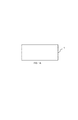
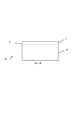
図1Aを参照にすると、以下に詳細に記載される基板から選択される支持基板1が、準備される。
Referring to FIG. 1A, a
図1Bを参照にすると、半導体層2を含むドナー基板20が準備される。
Referring to FIG. 1B, a
半導体層2の厚さは、典型的には10nmと10μmとの間にある。
The thickness of the
半導体層2は、好適には、シリコン、ゲルマニウム、又は1つ若しくは複数のIII族元素の窒化物(例えば、窒化ガリウム)、或いはInP若しくはAsGaなどのIII‐V族合金を含む。
The
層2は、特にバルク基板の場合、ドナー基板の一体化した部分であってもよい。
代替の実施形態では、層2は、エピタキシーによって基板22(この場合には層2の材料のエピタキシャル成長に適した基板22の材料)上に形成されていてもよいし、基板22上に接合されていてもよい。
In an alternative embodiment,
図1Cを参照にすると、半導体層2は支持基板1上に接合される。
Referring to FIG. 1C, the
任意選択で、ある層(ここには図示されていない)が、接合を容易にするために半導体層2上に形成されてもよい。
Optionally, a layer (not shown here) may be formed on the
この接合層は、意図された用途と適合する電気的及び/又は熱的特性を有し、接合を可能にする材料で作製されてもよい。例えば、接合層は、その接合層の厚さが50nmを超えないならば、アルミナ、AlN、高い電気抵抗性多結晶質シリコン、又は酸化シリコンからなってもよい。 This bonding layer may be made of a material that has electrical and / or thermal properties compatible with the intended use and that allows bonding. For example, the bonding layer may be made of alumina, AlN, high electrical resistance polycrystalline silicon, or silicon oxide if the thickness of the bonding layer does not exceed 50 nm.
図1Dを参照にすると、支持基板1上に半導体層2だけをとどめるように、ドナー基板20の一部22は除去される。
Referring to FIG. 1D, a
この移し替えは、典型的には、スマートカット(Smart−Cut)(登録商標)プロセスによって実行されてもよく、それによって、(図1Bに示されるように)ドナー基板20は、脆化ゾーン21を形成するように、移し替えられる層2の厚さに対応する深さに原子種の注入を前もって受けていることになる。接合後、脆化ゾーンに対して熱的及び/又は機械的応力を加えることは、残りの構造からのドナー基板の分離を目的として、そのドナー基板の劈開を可能にする。
This transfer may typically be performed by a Smart-Cut (R) process, whereby the donor substrate 20 (as shown in FIG. 1B) can become
あるいは、ドナー基板は、化学的及び/又は物理的エッチングによって得られる、そのドナー基板の裏面からの薄型化によって除去されてもよい。 Alternatively, the donor substrate may be removed by thinning from the back side of the donor substrate obtained by chemical and / or physical etching.
図1Eを参照にすると、構成要素は、当業者に知られた任意の技術によって、半導体層2に形成される。
Referring to FIG. 1E, the components are formed in the
このプロセスの実施に適しており、優れた電気抵抗率と優れた熱伝導率との両方を有する支持基板は、図2及び図3を参照にして次に記載される。 A support substrate suitable for carrying out this process and having both excellent electrical resistivity and excellent thermal conductivity will be described next with reference to FIGS.
支持基板1は、電子装置のための機械的支えを構成するベース層と、高い熱伝導率と高い電気抵抗率との両方を有するように選択された表面層とを有利に含む。
The
「表面」とは、その層が、半導体層2に最も近いベース層の側面上に位置することを意味する。
“Surface” means that the layer is located on the side of the base layer closest to the
しかしながら、いくつかの実施形態では、表面層を形成する手法次第で、ベース層は、表面層によって封入されてもよい。あるいは、表面層は、ベース層の両側上に成膜されてもよい。 However, in some embodiments, depending on the technique for forming the surface layer, the base layer may be encapsulated by the surface layer. Alternatively, the surface layer may be formed on both sides of the base layer.
表面層は少なくとも5μmの厚さを有する。 The surface layer has a thickness of at least 5 μm.
表面層は、高い熱伝導率と高い電気抵抗率との両方を有する。 The surface layer has both high thermal conductivity and high electrical resistivity.
好適には、表面層の熱伝導率は少なくとも30W/m Kであり、その表面層の電気抵抗率は少なくとも3000オーム・cmである。 Preferably, the thermal conductivity of the surface layer is at least 30 W / m K and the electrical resistivity of the surface layer is at least 3000 ohm · cm.
ベース層は、電子装置に対して十分な剛性を与えるように選択された厚さを有する。 The base layer has a thickness selected to provide sufficient rigidity for the electronic device.
ベース層は、好適には、支持基板全体を通した熱放散を可能にするために、高い熱伝導率(すなわち、少なくとも30W/m K)を有する。 The base layer preferably has a high thermal conductivity (ie, at least 30 W / m K) to allow heat dissipation throughout the support substrate.
しかしながら、ベース層は、半導体層から(少なくとも5μm厚さの表面層によって分離された半導体層から)比較的離れているので、そのベース層は、任意特定の電気抵抗率を示すことを必要としない。 However, since the base layer is relatively far from the semiconductor layer (from the semiconductor layer separated by a surface layer that is at least 5 μm thick), the base layer does not need to exhibit any particular electrical resistivity. .
特に、ベース層は、表面層の電気抵抗率よりも低い電気抵抗率を有してもよい。 In particular, the base layer may have an electrical resistivity lower than that of the surface layer.
この点において、ベース層は、大きな直径で利用可能である材料であって、サファイアよりも費用のかからない材料ででき得る一方で、より高い熱伝導率を示す。 In this respect, the base layer is a material that is available in large diameters and can be made of a material that is less expensive than sapphire, while exhibiting a higher thermal conductivity.
熱伝導率及び電気抵抗率の要求を切り離すことによって、従って、構成要素に最も近い5μm厚さの層における高い電気抵抗率と、高い熱伝導率とを示す支持基板を定義することが可能である。 By decoupling the requirements of thermal conductivity and electrical resistivity, it is therefore possible to define a support substrate that exhibits high electrical resistivity and high thermal conductivity in the 5 μm thick layer closest to the component. .
従って、電気抵抗率を規定する層と、熱伝導率を規定する層とを独立して選択することが可能である。 Therefore, it is possible to independently select the layer that defines the electrical resistivity and the layer that defines the thermal conductivity.
支持基板のいくつかの実施形態は、以下に記載される。
二重層支持基板
Some embodiments of the support substrate are described below.
Double layer support substrate
「二重層」とは、本文において、支持基板が、異なる熱伝導率及び電気抵抗率を有する少なくとも2つの層を含むことを意味する。 “Double layer” means herein that the support substrate comprises at least two layers having different thermal conductivities and electrical resistivities.
その少なくとも2つの層は、異なる材料でできていてもよい。 The at least two layers may be made of different materials.
図2を参照にすると、支持基板1は、高い熱伝導率を有する第1の材料でできたベース基板12であって、同じく高い熱伝導率を有するが何よりも高い電気抵抗率を有する第2の材料でできた表面層13で被覆された、ベース基板12を含む。
Referring to FIG. 2, the
第2の材料は、好適には、薄層2の半導体材料に対して優れた付着性を更に有する。
The second material preferably further has excellent adhesion to the semiconductor material of the
これが無い場合には、上記したような接合層が、その支持基板の表面上に設けられてもよい。 In the absence of this, the bonding layer as described above may be provided on the surface of the support substrate.
この基板1は、第2の材料の厚い層(すなわち、典型的には10μmよりも大きい厚さ、いずれにしても5μmよりも大きい厚さを有する層)13を第1の材料の基板12上に成膜することによって製造される。
The
1つの好適な実施形態によれば、第1の材料はシリコンであり、第2の材料はAlN又は非晶質の(DLCとして知られてもいる)ダイヤモンドライクカーボンである。 According to one preferred embodiment, the first material is silicon and the second material is AlN or amorphous (also known as DLC) diamond-like carbon.
これらの材料の成膜のための技術は、当業者に知られている。 Techniques for depositing these materials are known to those skilled in the art.
AlN成膜は、化学蒸着(CVD)及び特に高温化学蒸着(HTCVD)プロセスを含んでもよい。 AlN film formation may include chemical vapor deposition (CVD) and in particular high temperature chemical vapor deposition (HTCVD) processes.
AlN成膜に適した更なるプロセスは、パルス状のDCスパッタリングである。 A further process suitable for AlN deposition is pulsed DC sputtering.
非晶質ダイヤモンドライクカーボン成膜のために、以下の技術、すなわち、プラズマ促進化学蒸着(PECVD)、フィルター処理された陰極真空アーク(FCVA:filtered cathodic vacuum arc)技術、パルスレーザー成膜(PLD)が挙げられ得る。 For amorphous diamond-like carbon film formation, the following techniques: plasma enhanced chemical vapor deposition (PECVD), filtered cathodic vacuum arc (FCVA) technique, pulsed laser film formation (PLD) Can be mentioned.
任意選択で、基板1の厚い層13上に層2を接合すること考慮して、微細な酸化シリコン層3が層2上に形成されてもよい。
Optionally, a fine
前の事例に記載されたように、酸化物層は50nmよりも小さい厚さを有する。
改変された表面領域を有する支持基板
As described in the previous case, the oxide layer has a thickness of less than 50 nm.
Support substrate with modified surface area
本発明に係る支持基板を得るための代替の実施形態は、バルク基板に対して、熱伝導率及び/又は電気抵抗率の点で改善された特性を基板の表面領域に与える表面処理の利用を含む。 An alternative embodiment for obtaining a support substrate according to the present invention involves the use of a surface treatment that gives the surface region of the substrate improved properties in terms of thermal conductivity and / or electrical resistivity relative to the bulk substrate. Including.
この点において、ベース層及び表面層は同じ材料でできていてもよいが、表面層の電気抵抗率及び/又は熱伝導率がベース層の電気抵抗率及び/又は熱伝導率と異なるように、表面層の材料は、構造的に並びに/或いは化学的に及び/又は物理的に改変される。 In this respect, the base layer and the surface layer may be made of the same material, but the electrical resistivity and / or thermal conductivity of the surface layer is different from the electrical resistivity and / or thermal conductivity of the base layer, The material of the surface layer is modified structurally and / or chemically and / or physically.
より詳細には、バルクシリコン基板の表面は、表面上に、厚い、すなわちおよそ5μmの厚さを有する、多孔性表面層を形成するために、多孔を持たせられ(porosified)てもよい。 More particularly, the surface of the bulk silicon substrate may be porous to form a porous surface layer on the surface that is thick, ie having a thickness of approximately 5 μm.
多孔性表面層は、例えばHF型電解質における電気化学反応によって形成される。 The porous surface layer is formed by, for example, an electrochemical reaction in an HF electrolyte.
多孔を持たせられた領域において高い抵抗率を得ることは、この領域の形態構造と関連付けられる。 Obtaining a high resistivity in the porous region is associated with the morphological structure of this region.
従って、非常に高い電気抵抗率を有する基板の表面領域が形成されることを確実にすることが可能である。 It is thus possible to ensure that a surface area of the substrate having a very high electrical resistivity is formed.
図3は、そのような支持基板1上に構成要素の層2’を備える装置を例示し、層2’の下に位置する基板1の領域14は、非常に高い抵抗率を有する。
FIG. 3 illustrates a device comprising a
その上、その基板はシリコンでできているので、その基板は、意図された用途のための十分な熱伝導率を有する。
第2のプロセス:構成要素を支持する層の支持基板上への移し替え
Moreover, since the substrate is made of silicon, the substrate has sufficient thermal conductivity for the intended application.
Second process: transfer of the layer supporting the component onto the support substrate
第2のプロセスは、一般に、ドナー基板と呼ばれる基板の半導体層に構成要素を製造することと、構成要素を含む層を最終的な支持基板上に移し替えるために2度の移し替えを実行することとからなる。 The second process typically produces a component in a semiconductor layer of a substrate called a donor substrate and performs two transfers to transfer the layer containing the component onto the final support substrate. It consists of that.
図4Aに示されるように、半導体層2を含むドナー基板20が準備される。
As shown in FIG. 4A, a
半導体層2の厚さは、典型的には10nmと10μmとの間にある。
The thickness of the
半導体層2は、好適には、シリコン、ゲルマニウム、又は1つ若しくは複数のIII族元素の窒化物(例えば、窒化ガリウム)、或いは例えばInP若しくはAsGaなどのIII‐V族合金を含む。
The
層2は、特にバルク基板の場合には、ドナー基板の一体化した部分であってもよい。
代替の実施形態では、層2は、ドナー基板20を形成するために、エピタキシー(この場合には層2の材料のエピタキシャル成長に適した基板22の材料)によって基板22上に形成されていてもよいし、基板22上に接合されていてもよい。
In an alternative embodiment,
ドナー基板の材料は、構成要素の製造のために使用される高温に耐えるのに適している。 The donor substrate material is suitable to withstand the high temperatures used for the manufacture of the components.
その材料はまた、プロセスの様々なステップの間の取り扱いのために十分な剛性を全体に与えるべきでもある。 The material should also provide sufficient rigidity overall for handling during the various steps of the process.
本発明の1つの好適な実施形態によれば、ドナー基板は、絶縁体上の半導体(SOI:
semiconductor on insulator)型の基板であり、すなわち、機械的な基板として作用する第1の基板22と、50nmよりも小さい厚さを有する酸化シリコンの層又はAlN、アルミナ若しくは高抵抗性多結晶質シリコンの層であり得る埋め込まれた層23と、構成要素が製造される層2とを連続的に備える。
According to one preferred embodiment of the invention, the donor substrate is a semiconductor on insulator (SOI:
a
この実施形態は、図4Aから図4Fまでに例示される。 This embodiment is illustrated in FIGS. 4A to 4F.
図4Bを参照にすると、必要とされる構成要素は、当業者に知られたプロセスを用いて、半導体層2に及び/又は半導体層2上に製造される。
Referring to FIG. 4B, the required components are fabricated in and / or on the
図4Cを参照にすると、構成要素を含む半導体層2’は、中間基板4上に接合される。
Referring to FIG. 4C, the
この場合では、半導体層2’の構成要素は、その構成要素が製造された配置に対して逆にされた位置に見られる。 In this case, the components of the semiconductor layer 2 'are seen in the inverted position relative to the arrangement in which the components were manufactured.
図4Dを参照にすると、ドナー基板の残り22は、中間基板4上に、層23で被覆された構成要素を支持する層2’だけを残すように、除去される。
Referring to FIG. 4D, the
典型的には後に化学的エッチングが続く機械的なエッチングによって実行される、このドナー基板除去ステップにおいて、層23は、エッチング剤に対してバリア層として作用し、層2’を保護することを可能にする。
In this donor substrate removal step, typically performed by mechanical etching followed by chemical etching,
図4Eを参照にすると、前のステップにおいて得られた構造は、装置の最終的な支持基板である支持基板1上に接合され、層23は境界面に位置している。
Referring to FIG. 4E, the structure obtained in the previous step is bonded onto the
支持基板1は、本発明に係る基板であり、すなわち、少なくとも5μm厚さの表面層で、高い電気抵抗率と、高い熱伝導率との両方を有する基板である。
The
但し、ドナー基板の接合処理及び薄型化処理が、構成要素の製造よりも低い温度で実施されるならば、支持基板に加えられる熱応力は、第1のプロセスの場合よりも低い。 However, if the bonding process and thinning process of the donor substrate are performed at a lower temperature than the manufacturing of the component, the thermal stress applied to the support substrate is lower than in the first process.
この手法では、支持基板は、400℃と600℃との間の温度に耐えるべきであり、その支持基板の熱膨張係数の影響はまた、第1のプロセスの場合よりも低い。 In this approach, the support substrate should withstand temperatures between 400 ° C. and 600 ° C., and the effect of the coefficient of thermal expansion of the support substrate is also lower than in the first process.
プロセスの実施のために適した支持基板は、以下に記載される。 Suitable support substrates for performing the process are described below.
もちろん、第1のプロセスの実施のために考案された支持基板はまた、加えられる熱応力がより低いので、第2のプロセスに使用するのにも適している。 Of course, the support substrate devised for carrying out the first process is also suitable for use in the second process because the applied thermal stress is lower.
この接合ステップでは、層23は、支持基板1上への層2’の付着を容易にするための接合層として作用する。
In this bonding step, the
図4Fを参照にすると、中間基板4は、支持基板1上に、再び埋め込まれる層23と、構成要素を含む半導体層2’とだけを残すように除去される。
Referring to FIG. 4F, the intermediate substrate 4 is removed on the
従って、構成要素は、その構成要素が製造された配置に戻される。 Thus, the component is returned to the arrangement in which it was manufactured.
この除去ステップは、当業者に知られた任意の技術を用いて実施されてもよい。 This removal step may be performed using any technique known to those skilled in the art.
例えば、ドナー基板は、そのドナー基板の裏面からの薄型化であって、化学的及び/又は物理的エッチング(研磨)による材料除去を含む薄型化をされてもよい。 For example, the donor substrate may be thinned from the backside of the donor substrate, including material removal by chemical and / or physical etching (polishing).
構成要素を支持する層のこの移し替えプロセスを実施するために、そのプロセスの実施の例を記載する文献US6,911,375号に対して、参照がなされてもよい。 In order to carry out this transfer process of the layer supporting the component, reference may be made to document US Pat. No. 6,911,375 which describes an example of implementation of the process.
層23が酸化シリコンの層である場合、その層は、装置に熱障壁を形成しないように十分に薄いことが留意されるべきである。
It should be noted that if
高い電気抵抗率及び高い熱伝導率の両方を有し、このプロセスに使用するのに適した複数の支持基板は、次に記載される。
改変された表面層を有する支持基板
A plurality of support substrates having both high electrical resistivity and high thermal conductivity and suitable for use in this process will now be described.
Support substrate having a modified surface layer
図3に示される他の実施形態は、熱伝導率及び/又は電気抵抗率の点で改善された特性を基板の表面層に与える表面処理にさらされるバルク基板の使用を含む。 Another embodiment shown in FIG. 3 involves the use of a bulk substrate that is subjected to a surface treatment that provides the surface layer of the substrate with improved properties in terms of thermal conductivity and / or electrical resistivity.
この点において、多孔性表面層を有するシリコン支持基板は、この第2のプロセスの実施に適している。 In this respect, a silicon support substrate having a porous surface layer is suitable for carrying out this second process.
1つの代替案によれば、アルミニウム基板は、陽極処理されるか、窒化処理される。 According to one alternative, the aluminum substrate is anodized or nitrided.
陽極処理は、基板について厚さ数十μmまでのアルミナ被覆14の形成をもたらす。
Anodizing results in the formation of an
その上、形成される層が厚ければ厚いほど、その層の多孔性はより高くなる。 Moreover, the thicker the layer formed, the higher the porosity of that layer.
アルミニウム基板の窒化処理は、基板についてAlN被覆14の形成を引き起こす。
Nitriding of the aluminum substrate causes formation of the
そのようなAlN層を得る更なる手段は、基板を被覆するアルミナ層の炭素還元を実行することから成る。 A further means of obtaining such an AlN layer consists in performing a carbon reduction of the alumina layer covering the substrate.
このAlN層の厚さは、大きく、すなわち、典型的には5μmよりも大きい厚さを有する。 The thickness of this AlN layer is large, i.e. typically has a thickness greater than 5 μm.
更なる選択肢は、この層において1015at/cm3よりも高い金濃度を得るように、シリコン基板の上面の比較的かなり大きな厚さ(すなわち、少なくとも5μおよび好適には数十μm)にわたって、金を拡散することである。 A further option is that over a relatively large thickness of the top surface of the silicon substrate (ie at least 5 μm and preferably several tens of μm) so as to obtain a gold concentration higher than 10 15 at / cm 3 in this layer. It is to diffuse gold.
そのような支持基板は、例えば、金層をシリコン基板の上面上に成膜することによって、更に、シリコン基板のその厚さに金原子の拡散を引き起こす熱処理を加えることによって、得られる。 Such a support substrate can be obtained, for example, by depositing a gold layer on the upper surface of the silicon substrate, and further applying a heat treatment that causes diffusion of gold atoms to the thickness of the silicon substrate.
熱処理条件、特にその熱処理の期間は、金が、約5μmの厚さを超えて、更に、その基板の厚さ全体にわたらないで、基板の表面層だけに拡散するように、決定される。 The heat treatment conditions, particularly the duration of the heat treatment, are determined so that the gold diffuses only into the surface layer of the substrate, exceeding a thickness of about 5 μm and not over the entire thickness of the substrate.
論文「Semi‐insulating silicon for microwave devices」、D.M.Jordanら、Solid State Phenomena、第156〜158巻(2010)、第101〜106頁は、金を基板全体にわたって拡散することによってシリコン基板をドーピングするためのプロセスを開示するが、SOI型構造の形成のために、封入層の使用を必要とする。
得られた装置
Thesis “Semi-insulating silicon for microwave devices”, D.C. M.M. Jordan et al., Solid State Phenomena, 156-158 (2010), pages 101-106 disclose a process for doping a silicon substrate by diffusing gold throughout the substrate, but forming an SOI type structure. Requires the use of an encapsulation layer.
The resulting device
次に、図1E及び図4Fに一般に例示されるように、構成要素を支持する半導体層に最も近い層上で少なくとも高い電気抵抗率と、高い熱伝導率との両方を有する支持基板1上に、構成要素を支持する薄層2’を備えるウェハが得られる。
Next, as generally illustrated in FIGS. 1E and 4F, on a
特に、そのウェハは、そのウェハの構造において、熱障壁を備えていない。なぜなら、そのウェハの断熱性が支持基板内の熱放散を阻害しないように、構成要素を支持する層と支持基板との間に配置された任意の接合層が、断熱材として作用しない材料(例えばAl、AlN又は高抵抗性多結晶質シリコン)、又は十分に微細な(すなわち、50nmよりも小さい厚さを有する)酸化シリコンでできているからである。 In particular, the wafer does not have a thermal barrier in the structure of the wafer. This is because any bonding layer disposed between the layer supporting the component and the support substrate does not act as a thermal insulator (e.g., so that the thermal insulation of the wafer does not hinder heat dissipation in the support substrate (e.g. This is because it is made of silicon oxide (Al, AlN or high-resistance polycrystalline silicon) or sufficiently fine (that is, having a thickness of less than 50 nm).
図2及び図3は、支持基板の性質に従って、ウェハの様々な実施形態を例示する。 2 and 3 illustrate various embodiments of the wafer according to the nature of the support substrate.
ウェハは、150mmよりも大きい、好適には200mmよりも大きい直径を有利に有する。 The wafer advantageously has a diameter greater than 150 mm, preferably greater than 200 mm.
更にまた、ウェハは、個々のチップに分離するためにそのウェハの厚さに沿って切断されてもよく、その切断技術は当業者に知られている。 Furthermore, the wafer may be cut along the thickness of the wafer for separation into individual chips, the cutting techniques being known to those skilled in the art.
チップの形成はまた、支持基板の薄型化も含んでもよい。 Chip formation may also include thinning the support substrate.
実際、その基板は、プロセスを実施するためのステップの間に十分な剛性を表わすために比較的かなり大きな厚さ(典型的には、およそ1mm)で提供されるが、チップは、より薄い支持基板(典型的には、およそ50μmまたは20μm)を用いて機能してもよい。 In fact, the substrate is provided with a relatively large thickness (typically around 1 mm) to exhibit sufficient rigidity during the steps to carry out the process, but the chip has a thinner support. A substrate (typically approximately 50 μm or 20 μm) may be used.
最後に、上記で与えられた例は、本発明の用途の分野に関して決して限定的ではない単なる特定の例示に過ぎないことは明白である。 Finally, it is clear that the examples given above are merely specific illustrations that are in no way limiting with respect to the field of application of the present invention.
1…支持基板、2、2’…半導体層、3、23…接合層、12…ベース層、13、14…表面層。
DESCRIPTION OF
Claims (2)
(a)ドナー基板(20)の半導体層(2)における前記電子構成要素を製造するステップと、
(b)前記電子構成要素を支持する前記層(2’)を中間基板(4)上に接合するステップと、
(c)前記電子構成要素を支持する前記層(2’)を前記中間基板(4)上に移し替えるために前記ドナー基板(20)の残り(22)を除去するステップと、
(d)前記電子構成要素を支持する前記層(2’)を前記支持基板(1)上に接合するステップと、
(e)前記中間基板(4)を除去するステップとを含む、プロセスにおいて、
接合層(23)が、前記支持基板(1)と前記電子構成要素を支持する前記層(2’)との間にあり、前記接合層(23)が、50nmよりも小さい厚さを有する酸化シリコン層、AlNの層、アルミナの層又は高抵抗性多結晶質シリコンの層からなり、ステップ(d)では、少なくとも30W/mKの熱伝導率を有するベース層(12)と、少なくとも5μmの厚さを有する表面層(13、14)とを含む支持基板(1)であって、前記表面層が、少なくとも3000オーム・cmの電気抵抗率と、少なくとも30W/mKの熱伝導率とを有する、支持基板(1)が使用され、前記支持基板(1)は、前記表面層として表面領域を含み、前記表面領域は、1015at/cm3よりも高い濃度で金をドープされており、5μmよりも大きい厚さを有する、ことを特徴とする、プロセス。 A process for manufacturing a device for radio frequency or power applications comprising a layer (2 ') supporting an electronic component on a support substrate (1), comprising the following sequential steps:
(A) manufacturing the electronic component in the semiconductor layer (2) of the donor substrate (20);
(B) bonding the layer (2 ′) supporting the electronic component onto the intermediate substrate (4);
(C) removing the remainder (22) of the donor substrate (20) to transfer the layer (2 ′) supporting the electronic component onto the intermediate substrate (4);
(D) bonding the layer (2 ′) supporting the electronic component onto the support substrate (1);
(E) removing the intermediate substrate (4);
A bonding layer (23) is between the support substrate (1) and the layer (2 ′) supporting the electronic component, and the bonding layer (23) has an oxidation thickness less than 50 nm. The step (d) comprises a base layer (12) having a thermal conductivity of at least 30 W / mK and a thickness of at least 5 μm. A surface substrate (13, 14) having a thickness, wherein the surface layer has an electrical resistivity of at least 3000 ohm · cm and a thermal conductivity of at least 30 W / mK. A support substrate (1) is used, the support substrate (1) comprising a surface region as the surface layer, the surface region being doped with gold at a concentration higher than 10 15 at / cm 3 , 5 μm Bigger than It is having of, characterized in that the process.
Applications Claiming Priority (2)
| Application Number | Priority Date | Filing Date | Title |
|---|---|---|---|
| FR1059539 | 2010-11-19 | ||
| FR1059539A FR2967812B1 (en) | 2010-11-19 | 2010-11-19 | ELECTRONIC DEVICE FOR RADIOFREQUENCY OR POWER APPLICATIONS AND METHOD OF MANUFACTURING SUCH A DEVICE |
Related Parent Applications (1)
| Application Number | Title | Priority Date | Filing Date |
|---|---|---|---|
| JP2013539237A Division JP6089252B2 (en) | 2010-11-19 | 2011-11-16 | Electronic devices for radio frequency or power applications and processes for manufacturing such devices |
Publications (2)
| Publication Number | Publication Date |
|---|---|
| JP2016219833A JP2016219833A (en) | 2016-12-22 |
| JP6286780B2 true JP6286780B2 (en) | 2018-03-07 |
Family
ID=44041749
Family Applications (2)
| Application Number | Title | Priority Date | Filing Date |
|---|---|---|---|
| JP2013539237A Active JP6089252B2 (en) | 2010-11-19 | 2011-11-16 | Electronic devices for radio frequency or power applications and processes for manufacturing such devices |
| JP2016159361A Active JP6286780B2 (en) | 2010-11-19 | 2016-08-15 | Electronic devices for radio frequency or power applications and processes for manufacturing such devices |
Family Applications Before (1)
| Application Number | Title | Priority Date | Filing Date |
|---|---|---|---|
| JP2013539237A Active JP6089252B2 (en) | 2010-11-19 | 2011-11-16 | Electronic devices for radio frequency or power applications and processes for manufacturing such devices |
Country Status (9)
| Country | Link |
|---|---|
| US (1) | US9198294B2 (en) |
| EP (1) | EP2641265B1 (en) |
| JP (2) | JP6089252B2 (en) |
| KR (1) | KR101876912B1 (en) |
| CN (1) | CN103168342B (en) |
| FR (1) | FR2967812B1 (en) |
| SG (1) | SG189443A1 (en) |
| TW (1) | TWI503951B (en) |
| WO (1) | WO2012066021A1 (en) |
Families Citing this family (46)
| Publication number | Priority date | Publication date | Assignee | Title |
|---|---|---|---|---|
| KR20140118984A (en) * | 2011-11-04 | 2014-10-08 | 더 실라나 그룹 피티와이 리미티드 | Method of producing a silicon-on-insulator article |
| CN103703542B (en) * | 2012-07-18 | 2016-06-08 | 日本碍子株式会社 | Composite crystal and manufacture method thereof |
| FR2995444B1 (en) * | 2012-09-10 | 2016-11-25 | Soitec Silicon On Insulator | METHOD FOR DETACHING A LAYER |
| JP6024400B2 (en) | 2012-11-07 | 2016-11-16 | ソニー株式会社 | Semiconductor device, method for manufacturing semiconductor device, and antenna switch module |
| US10703627B2 (en) | 2013-06-27 | 2020-07-07 | Soitec | Methods of fabricating semiconductor structures including cavities filled with a sacrificial material |
| FI130149B (en) * | 2013-11-26 | 2023-03-15 | Okmetic Oyj | High-resistive silicon substrate with a reduced radio frequency loss for a radio-frequency integrated passive device |
| US10079170B2 (en) | 2014-01-23 | 2018-09-18 | Globalwafers Co., Ltd. | High resistivity SOI wafers and a method of manufacturing thereof |
| US20150371905A1 (en) * | 2014-06-20 | 2015-12-24 | Rf Micro Devices, Inc. | Soi with gold-doped handle wafer |
| FR3024587B1 (en) * | 2014-08-01 | 2018-01-26 | Soitec | METHOD FOR MANUFACTURING HIGHLY RESISTIVE STRUCTURE |
| US9853133B2 (en) * | 2014-09-04 | 2017-12-26 | Sunedison Semiconductor Limited (Uen201334164H) | Method of manufacturing high resistivity silicon-on-insulator substrate |
| US9899499B2 (en) | 2014-09-04 | 2018-02-20 | Sunedison Semiconductor Limited (Uen201334164H) | High resistivity silicon-on-insulator wafer manufacturing method for reducing substrate loss |
| US10224233B2 (en) | 2014-11-18 | 2019-03-05 | Globalwafers Co., Ltd. | High resistivity silicon-on-insulator substrate comprising a charge trapping layer formed by He-N2 co-implantation |
| EP3221885B1 (en) | 2014-11-18 | 2019-10-23 | GlobalWafers Co., Ltd. | High resistivity semiconductor-on-insulator wafer and a method of manufacturing |
| EP3221884B1 (en) | 2014-11-18 | 2022-06-01 | GlobalWafers Co., Ltd. | High resistivity semiconductor-on-insulator wafers with charge trapping layers and method of manufacturing thereof |
| JP6345107B2 (en) * | 2014-12-25 | 2018-06-20 | ルネサスエレクトロニクス株式会社 | Semiconductor device and manufacturing method thereof |
| EP4120320A1 (en) | 2015-03-03 | 2023-01-18 | GlobalWafers Co., Ltd. | Charge trapping polycrystalline silicon films on silicon substrates with controllable film stress |
| US10032870B2 (en) * | 2015-03-12 | 2018-07-24 | Globalfoundries Inc. | Low defect III-V semiconductor template on porous silicon |
| US9881832B2 (en) | 2015-03-17 | 2018-01-30 | Sunedison Semiconductor Limited (Uen201334164H) | Handle substrate for use in manufacture of semiconductor-on-insulator structure and method of manufacturing thereof |
| WO2016149113A1 (en) | 2015-03-17 | 2016-09-22 | Sunedison Semiconductor Limited | Thermally stable charge trapping layer for use in manufacture of semiconductor-on-insulator structures |
| WO2016196060A1 (en) | 2015-06-01 | 2016-12-08 | Sunedison Semiconductor Limited | A method of manufacturing semiconductor-on-insulator |
| US10332782B2 (en) | 2015-06-01 | 2019-06-25 | Globalwafers Co., Ltd. | Method of manufacturing silicon germanium-on-insulator |
| FR3037443B1 (en) | 2015-06-12 | 2018-07-13 | Soitec | HETEROSTRUCTURE AND METHOD OF MANUFACTURE |
| US10529616B2 (en) | 2015-11-20 | 2020-01-07 | Globalwafers Co., Ltd. | Manufacturing method of smoothing a semiconductor surface |
| US10468294B2 (en) | 2016-02-19 | 2019-11-05 | Globalwafers Co., Ltd. | High resistivity silicon-on-insulator substrate comprising a charge trapping layer formed on a substrate with a rough surface |
| US9831115B2 (en) | 2016-02-19 | 2017-11-28 | Sunedison Semiconductor Limited (Uen201334164H) | Process flow for manufacturing semiconductor on insulator structures in parallel |
| US10622247B2 (en) | 2016-02-19 | 2020-04-14 | Globalwafers Co., Ltd. | Semiconductor on insulator structure comprising a buried high resistivity layer |
| US10573550B2 (en) | 2016-03-07 | 2020-02-25 | Globalwafers Co., Ltd. | Semiconductor on insulator structure comprising a plasma oxide layer and method of manufacture thereof |
| WO2017155808A1 (en) | 2016-03-07 | 2017-09-14 | Sunedison Semiconductor Limited | Semiconductor on insulator structure comprising a plasma nitride layer and method of manufacture thereof |
| EP3427293B1 (en) | 2016-03-07 | 2021-05-05 | Globalwafers Co., Ltd. | Semiconductor on insulator structure comprising a low temperature flowable oxide layer and method of manufacture thereof |
| US11848227B2 (en) | 2016-03-07 | 2023-12-19 | Globalwafers Co., Ltd. | Method of manufacturing a semiconductor on insulator structure by a pressurized bond treatment |
| US10354910B2 (en) * | 2016-05-27 | 2019-07-16 | Raytheon Company | Foundry-agnostic post-processing method for a wafer |
| CN116314384A (en) | 2016-06-08 | 2023-06-23 | 环球晶圆股份有限公司 | High resistivity single crystal silicon ingot and wafer with improved mechanical strength |
| US10269617B2 (en) | 2016-06-22 | 2019-04-23 | Globalwafers Co., Ltd. | High resistivity silicon-on-insulator substrate comprising an isolation region |
| CN115763496A (en) | 2016-10-26 | 2023-03-07 | 环球晶圆股份有限公司 | High resistivity silicon-on-insulator substrate with enhanced charge trapping efficiency |
| WO2018083961A1 (en) * | 2016-11-01 | 2018-05-11 | 信越化学工業株式会社 | Method for transferring device layer to transfer substrate and highly heat conductive substrate |
| EP3549162B1 (en) | 2016-12-05 | 2022-02-02 | GlobalWafers Co., Ltd. | High resistivity silicon-on-insulator structure and method of manufacture thereof |
| SG10201913071XA (en) | 2016-12-28 | 2020-03-30 | Sunedison Semiconductor Ltd | Method of treating silicon wafers to have intrinsic gettering and gate oxide integrity yield |
| WO2018182680A1 (en) * | 2017-03-31 | 2018-10-04 | Intel Corporation | Thermally resistive intercalation layers in a resistive switch device |
| US10388518B2 (en) * | 2017-03-31 | 2019-08-20 | Globalwafers Co., Ltd. | Epitaxial substrate and method of manufacturing the same |
| WO2019013904A1 (en) | 2017-07-14 | 2019-01-17 | Globalwafers Co., Ltd. | Method of manufacture of a semiconductor on insulator structure |
| CN112655083A (en) | 2018-04-27 | 2021-04-13 | 环球晶圆股份有限公司 | Photo-assisted sheet formation to facilitate layer transfer from a semiconductor donor substrate |
| WO2019236320A1 (en) | 2018-06-08 | 2019-12-12 | Globalwafers Co., Ltd. | Method for transfer of a thin layer of silicon |
| TWI698029B (en) * | 2018-11-28 | 2020-07-01 | 財團法人金屬工業研究發展中心 | Method of forming semiconductor structure |
| WO2021015816A1 (en) * | 2019-07-19 | 2021-01-28 | Iqe Plc | Semiconductor material having tunable permittivity and tunable thermal conductivity |
| JP7192757B2 (en) * | 2019-12-19 | 2022-12-20 | 株式会社Sumco | Epitaxial silicon wafer, manufacturing method thereof, and X-ray detection sensor |
| CN112113449B (en) * | 2020-09-04 | 2022-05-20 | Oppo广东移动通信有限公司 | Vapor chamber, method for manufacturing vapor chamber, electronic device, and electronic apparatus |
Family Cites Families (32)
| Publication number | Priority date | Publication date | Assignee | Title |
|---|---|---|---|---|
| JPS5624163U (en) * | 1979-08-01 | 1981-03-04 | ||
| US5053283A (en) * | 1988-12-23 | 1991-10-01 | Spectrol Electronics Corporation | Thick film ink composition |
| IT1268123B1 (en) * | 1994-10-13 | 1997-02-20 | Sgs Thomson Microelectronics | SLICE OF SEMICONDUCTOR MATERIAL FOR THE MANUFACTURE OF INTEGRATED DEVICES AND PROCEDURE FOR ITS MANUFACTURING. |
| US5773151A (en) * | 1995-06-30 | 1998-06-30 | Harris Corporation | Semi-insulating wafer |
| JPH10335615A (en) * | 1997-05-22 | 1998-12-18 | Harris Corp | Improvement of semiconductor device |
| JP3809733B2 (en) * | 1998-02-25 | 2006-08-16 | セイコーエプソン株式会社 | Thin film transistor peeling method |
| FR2781082B1 (en) * | 1998-07-10 | 2002-09-20 | Commissariat Energie Atomique | SEMICONDUCTOR THIN-LAYER STRUCTURE HAVING A HEAT-DISTRIBUTING LAYER |
| US20020089016A1 (en) * | 1998-07-10 | 2002-07-11 | Jean-Pierre Joly | Thin layer semi-conductor structure comprising a heat distribution layer |
| JP4556255B2 (en) * | 1998-12-07 | 2010-10-06 | 株式会社デンソー | Manufacturing method of semiconductor device |
| US6323108B1 (en) * | 1999-07-27 | 2001-11-27 | The United States Of America As Represented By The Secretary Of The Navy | Fabrication ultra-thin bonded semiconductor layers |
| JP2002299263A (en) * | 2001-04-03 | 2002-10-11 | Matsushita Electric Ind Co Ltd | Manufacturing method for semiconductor device |
| US6717212B2 (en) * | 2001-06-12 | 2004-04-06 | Advanced Micro Devices, Inc. | Leaky, thermally conductive insulator material (LTCIM) in semiconductor-on-insulator (SOI) structure |
| US7148079B1 (en) * | 2002-11-01 | 2006-12-12 | Advanced Micro Devices, Inc. | Diamond like carbon silicon on insulator substrates and methods of fabrication thereof |
| JP3551187B2 (en) | 2002-11-28 | 2004-08-04 | セイコーエプソン株式会社 | Optical element, illumination device, and projection display device |
| FR2851079B1 (en) * | 2003-02-12 | 2005-08-26 | Soitec Silicon On Insulator | SEMICONDUCTOR STRUCTURE ON SUBSTRATE WITH HIGH ROUGHNESS |
| US6911375B2 (en) | 2003-06-02 | 2005-06-28 | International Business Machines Corporation | Method of fabricating silicon devices on sapphire with wafer bonding at low temperature |
| DE10326578B4 (en) * | 2003-06-12 | 2006-01-19 | Siltronic Ag | Process for producing an SOI disk |
| FR2857983B1 (en) * | 2003-07-24 | 2005-09-02 | Soitec Silicon On Insulator | PROCESS FOR PRODUCING AN EPITAXIC LAYER |
| EP1665367A2 (en) | 2003-09-26 | 2006-06-07 | Universite Catholique De Louvain | Method of manufacturing a multilayer semiconductor structure with reduced ohmic losses |
| US9813152B2 (en) * | 2004-01-14 | 2017-11-07 | Luxtera, Inc. | Method and system for optoelectronics transceivers integrated on a CMOS chip |
| FR2871172B1 (en) * | 2004-06-03 | 2006-09-22 | Soitec Silicon On Insulator | HYBRID EPITAXIS SUPPORT AND METHOD OF MANUFACTURING THE SAME |
| JP4559839B2 (en) | 2004-12-13 | 2010-10-13 | トヨタ自動車株式会社 | Manufacturing method of semiconductor device |
| JP2007012897A (en) * | 2005-06-30 | 2007-01-18 | Nec Electronics Corp | Semiconductor device and method of manufacturing same |
| CN101548369B (en) * | 2006-12-26 | 2012-07-18 | 硅绝缘体技术有限公司 | Method for producing a semiconductor-on-insulator structure |
| JP4380709B2 (en) * | 2007-01-31 | 2009-12-09 | セイコーエプソン株式会社 | Manufacturing method of semiconductor device |
| JP2009027604A (en) | 2007-07-23 | 2009-02-05 | Elmo Co Ltd | Noise reducer, and noise reducing method |
| US20090278233A1 (en) * | 2007-07-26 | 2009-11-12 | Pinnington Thomas Henry | Bonded intermediate substrate and method of making same |
| FR2933233B1 (en) | 2008-06-30 | 2010-11-26 | Soitec Silicon On Insulator | GOOD RESISTANCE HIGH RESISTIVITY SUBSTRATE AND METHOD FOR MANUFACTURING THE SAME |
| US8367520B2 (en) * | 2008-09-22 | 2013-02-05 | Soitec | Methods and structures for altering strain in III-nitride materials |
| FR2947380B1 (en) * | 2009-06-26 | 2012-12-14 | Soitec Silicon Insulator Technologies | METHOD OF COLLAGE BY MOLECULAR ADHESION. |
| FR2950734B1 (en) * | 2009-09-28 | 2011-12-09 | Soitec Silicon On Insulator | METHOD FOR BONDING AND TRANSFERRING A LAYER |
| TWM389354U (en) * | 2010-05-05 | 2010-09-21 | Paragon Technologies Co Ltd | Substrate with metallized surface |
-
2010
- 2010-11-19 FR FR1059539A patent/FR2967812B1/en active Active
-
2011
- 2011-11-15 TW TW100141594A patent/TWI503951B/en active
- 2011-11-16 EP EP11782165.2A patent/EP2641265B1/en active Active
- 2011-11-16 CN CN201180050082.5A patent/CN103168342B/en active Active
- 2011-11-16 SG SG2013028956A patent/SG189443A1/en unknown
- 2011-11-16 WO PCT/EP2011/070220 patent/WO2012066021A1/en active Application Filing
- 2011-11-16 US US13/989,751 patent/US9198294B2/en active Active
- 2011-11-16 JP JP2013539237A patent/JP6089252B2/en active Active
- 2011-11-16 KR KR1020137015796A patent/KR101876912B1/en active IP Right Grant
-
2016
- 2016-08-15 JP JP2016159361A patent/JP6286780B2/en active Active
Also Published As
| Publication number | Publication date |
|---|---|
| JP2013543276A (en) | 2013-11-28 |
| CN103168342A (en) | 2013-06-19 |
| WO2012066021A4 (en) | 2012-07-19 |
| KR101876912B1 (en) | 2018-07-11 |
| EP2641265A1 (en) | 2013-09-25 |
| US9198294B2 (en) | 2015-11-24 |
| TWI503951B (en) | 2015-10-11 |
| US20130294038A1 (en) | 2013-11-07 |
| CN103168342B (en) | 2015-09-30 |
| SG189443A1 (en) | 2013-05-31 |
| JP2016219833A (en) | 2016-12-22 |
| KR20140005900A (en) | 2014-01-15 |
| WO2012066021A1 (en) | 2012-05-24 |
| EP2641265B1 (en) | 2019-01-02 |
| JP6089252B2 (en) | 2017-03-08 |
| FR2967812B1 (en) | 2016-06-10 |
| FR2967812A1 (en) | 2012-05-25 |
| TW201225256A (en) | 2012-06-16 |
Similar Documents
| Publication | Publication Date | Title |
|---|---|---|
| JP6286780B2 (en) | Electronic devices for radio frequency or power applications and processes for manufacturing such devices | |
| JP6650463B2 (en) | Method of manufacturing high resistivity semiconductor-on-insulator wafer with charge trapping layer | |
| JP6831911B2 (en) | High resistivity silicon-on-insulator substrate with improved charge capture efficiency | |
| US7939428B2 (en) | Methods for making substrates and substrates formed therefrom | |
| TWI280661B (en) | CMOS fabricated on different crystallographic orientation substrates | |
| JP2019153797A (en) | Method of growing charge trapping polycrystalline silicon films on silicon substrates with controllable film stress | |
| US7749863B1 (en) | Thermal management substrates | |
| US20190131169A1 (en) | High resistivity silicon-on-insulator wafer manufacturing method for reducing substrate loss | |
| JPH02290045A (en) | Method of forming insulating layer from non-silicon semicondutor layer | |
| US11251265B2 (en) | Carrier for a semiconductor structure | |
| US9142448B2 (en) | Method of producing a silicon-on-insulator article | |
| TWI241653B (en) | SOI structure with recess resistant buried insulator and manufacture method thereof | |
| JP2020113792A (en) | High resistivity semiconductor-on-insulator wafer and manufacturing method | |
| JP2008526009A (en) | How to move a circuit to a ground plane | |
| US7695564B1 (en) | Thermal management substrate | |
| KR100662694B1 (en) | Thin-layered semiconductor structure comprising a heat distribution layer | |
| KR20220163388A (en) | Composite substrate and its manufacturing method | |
| TW200527507A (en) | Semiconductor member, manufacturing method thereof, and semiconductor device | |
| TW201729339A (en) | Semiconductor on insulator substrate | |
| JP7186872B2 (en) | Semiconductor substrate manufacturing method and semiconductor device manufacturing method | |
| TWI751352B (en) | Substrate for an integrated radiofrequency device and method for manufacturing same | |
| WO2023045129A1 (en) | Manufacturing method for semiconductor structure and semiconductor structure | |
| US10600635B2 (en) | Method and apparatus for a semiconductor-on-higher thermal conductive multi-layer composite wafer | |
| JPS61144037A (en) | Semiconductor device and manufacture thereof | |
| JP2012114376A (en) | Manufacturing method of soi substrate |
Legal Events
| Date | Code | Title | Description |
|---|---|---|---|
| A977 | Report on retrieval |
Free format text: JAPANESE INTERMEDIATE CODE: A971007 Effective date: 20170420 |
|
| A131 | Notification of reasons for refusal |
Free format text: JAPANESE INTERMEDIATE CODE: A131 Effective date: 20170425 |
|
| A521 | Request for written amendment filed |
Free format text: JAPANESE INTERMEDIATE CODE: A523 Effective date: 20170719 |
|
| TRDD | Decision of grant or rejection written | ||
| A01 | Written decision to grant a patent or to grant a registration (utility model) |
Free format text: JAPANESE INTERMEDIATE CODE: A01 Effective date: 20180109 |
|
| A61 | First payment of annual fees (during grant procedure) |
Free format text: JAPANESE INTERMEDIATE CODE: A61 Effective date: 20180118 |
|
| R150 | Certificate of patent or registration of utility model |
Ref document number: 6286780 Country of ref document: JP Free format text: JAPANESE INTERMEDIATE CODE: R150 |
|
| R250 | Receipt of annual fees |
Free format text: JAPANESE INTERMEDIATE CODE: R250 |
|
| R250 | Receipt of annual fees |
Free format text: JAPANESE INTERMEDIATE CODE: R250 |
|
| R250 | Receipt of annual fees |
Free format text: JAPANESE INTERMEDIATE CODE: R250 |
|
| R250 | Receipt of annual fees |
Free format text: JAPANESE INTERMEDIATE CODE: R250 |