JP6271812B2 - Transparent pixel format converter - Google Patents
Transparent pixel format converter Download PDFInfo
- Publication number
- JP6271812B2 JP6271812B2 JP2017517240A JP2017517240A JP6271812B2 JP 6271812 B2 JP6271812 B2 JP 6271812B2 JP 2017517240 A JP2017517240 A JP 2017517240A JP 2017517240 A JP2017517240 A JP 2017517240A JP 6271812 B2 JP6271812 B2 JP 6271812B2
- Authority
- JP
- Japan
- Prior art keywords
- data
- format
- address
- processor
- data format
- Prior art date
- Legal status (The legal status is an assumption and is not a legal conclusion. Google has not performed a legal analysis and makes no representation as to the accuracy of the status listed.)
- Expired - Fee Related
Links
Images


Classifications
-
- G—PHYSICS
- G06—COMPUTING; CALCULATING OR COUNTING
- G06T—IMAGE DATA PROCESSING OR GENERATION, IN GENERAL
- G06T1/00—General purpose image data processing
- G06T1/60—Memory management
-
- G—PHYSICS
- G06—COMPUTING; CALCULATING OR COUNTING
- G06F—ELECTRIC DIGITAL DATA PROCESSING
- G06F12/00—Accessing, addressing or allocating within memory systems or architectures
- G06F12/02—Addressing or allocation; Relocation
- G06F12/08—Addressing or allocation; Relocation in hierarchically structured memory systems, e.g. virtual memory systems
- G06F12/10—Address translation
- G06F12/1027—Address translation using associative or pseudo-associative address translation means, e.g. translation look-aside buffer [TLB]
- G06F12/1036—Address translation using associative or pseudo-associative address translation means, e.g. translation look-aside buffer [TLB] for multiple virtual address spaces, e.g. segmentation
-
- G—PHYSICS
- G06—COMPUTING; CALCULATING OR COUNTING
- G06F—ELECTRIC DIGITAL DATA PROCESSING
- G06F12/00—Accessing, addressing or allocating within memory systems or architectures
- G06F12/02—Addressing or allocation; Relocation
- G06F12/08—Addressing or allocation; Relocation in hierarchically structured memory systems, e.g. virtual memory systems
- G06F12/10—Address translation
- G06F12/109—Address translation for multiple virtual address spaces, e.g. segmentation
-
- G—PHYSICS
- G06—COMPUTING; CALCULATING OR COUNTING
- G06T—IMAGE DATA PROCESSING OR GENERATION, IN GENERAL
- G06T1/00—General purpose image data processing
- G06T1/20—Processor architectures; Processor configuration, e.g. pipelining
-
- G—PHYSICS
- G06—COMPUTING; CALCULATING OR COUNTING
- G06F—ELECTRIC DIGITAL DATA PROCESSING
- G06F2212/00—Indexing scheme relating to accessing, addressing or allocation within memory systems or architectures
- G06F2212/65—Details of virtual memory and virtual address translation
- G06F2212/657—Virtual address space management
-
- G—PHYSICS
- G06—COMPUTING; CALCULATING OR COUNTING
- G06T—IMAGE DATA PROCESSING OR GENERATION, IN GENERAL
- G06T2200/00—Indexing scheme for image data processing or generation, in general
- G06T2200/28—Indexing scheme for image data processing or generation, in general involving image processing hardware
Description
[0001] 本開示は、透過的画素フォーマット変換器に関する。 [0001] The present disclosure relates to a transparent pixel format converter.
[0002] グラフィックス画像またはビデオのフレームのようなグラフィックスデータは、複数の画素から成り立ち得る。グラフィックスデータの画素に関する情報のような画素データは、1画素のデータに関連付けられたメモリのビットの数を規定し得、またこの画素のデータ内のカラー成分の順序を規定し得る、指定された画素フォーマットに従って配列され得る。指定された画素フォーマットに従ってメモリに配列される画素データはこの画素フォーマットに従って圧縮され得、またこの画素フォーマットに従ってこのメモりの複数のメモリロケーションに配列され得る。一般に、画素フォーマットは線形画素フォーマットまたはタイルベース画素フォーマットに分類される。 [0002] Graphics data, such as a graphics image or a frame of video, may consist of a plurality of pixels. Pixel data, such as information about a pixel of graphics data, is specified, which can define the number of bits of memory associated with the data of one pixel and can define the order of color components in the data of this pixel Can be arranged according to different pixel formats. Pixel data arranged in memory according to a specified pixel format may be compressed according to this pixel format and arranged in a plurality of memory locations of this memory according to this pixel format. In general, the pixel format is classified into a linear pixel format or a tile-based pixel format.
[0003] 一般に、本開示は、異なる画素フォーマット相互間で透過的に変換する透過的フォーマット変換器(TFC)に関し、TFCがグラフィックスデータの基底(underlying)画素フォーマットにかかわらずに、処理コアによってサポートされた画素フォーマットに従うグラフィックスデータのビュー(view)をもつ処理コアを提供し得る。TFCは処理コアが、処理コアによってサポートされた画素フォーマットに従ってグラフィックスデータが整列されるようにグラフィックスデータを扱うことを可能にし得る。 [0003] In general, this disclosure relates to a transparent format converter (TFC) that transparently converts between different pixel formats, regardless of the underlying pixel format of the graphics data by the processing core. A processing core having a view of graphics data according to a supported pixel format may be provided. TFC may allow a processing core to handle graphics data such that the graphics data is aligned according to the pixel format supported by the processing core.
[0004] 一態様において、本開示は画素処理のための方法に向けられている。この方法は、第1のデータバッファに保存されたデータに関する、少なくとも1つのプロセッサによる要求が第1のデータフォーマットにあるこのデータに関する要求を示すものであると、透過的フォーマット変換器(TFC)によって、決定することを含み得る。方法は、第1のデータバッファに保存されたデータに関する要求に少なくとも一部基づいて、第2のデータフォーマットにあるこのデータを第1のデータバッファから、TFCによって、取得することをさらに含み得る。方法は、取得されたデータを第2のデータフォーマットから第1のデータフォーマットへ、TFCによって、変換することをさらに含み得る。方法は、第1のデータフォーマットにある変換されたデータを、少なくとも1つのプロセッサによってアクセス可能である第2のデータバッファに、TFCによって、保存することをさらに含み得る。 [0004] In one aspect, the present disclosure is directed to a method for pixel processing. The method includes a transparent format converter (TFC) that requests for at least one processor for data stored in a first data buffer to indicate a request for this data in a first data format. , May include determining. The method may further include obtaining this data in the second data format from the first data buffer by TFC based at least in part on the request for data stored in the first data buffer. The method may further include converting the acquired data from the second data format to the first data format by TFC. The method may further include storing, by TFC, the converted data in the first data format in a second data buffer accessible by at least one processor.
[0005] 別の態様において、本開示は計算デバイスに向けられている。 この計算デバイスは、第1のデータバッファを含み得る。計算デバイスは、第2のデータバッファをさらに含み得る。計算デバイスは、少なくとも1つのプロセッサをさらに含み得る。計算デバイスは、第1のデータバッファに保存されたデータに関する、少なくとも1つのプロセッサによる要求が第1のデータフォーマットにあるこのデータに関する要求を示すものであると決定し、第1のデータバッファに保存されたデータに関する要求に少なくとも一部基づいて、第2のデータフォーマットにあるこのデータを第1のデータバッファから取得し、取得されたデータを第2のデータフォーマットから第1のデータフォーマットへ変換し、第1のデータフォーマットにある変換されたデータを、少なくとも1つのプロセッサによってアクセス可能である第2のデータバッファに保存するように構成される透過的フォーマット変換器をさらに含み得る。 [0005] In another aspect, the present disclosure is directed to a computing device. The computing device can include a first data buffer. The computing device may further include a second data buffer. The computing device may further include at least one processor. The computing device determines that the request by the at least one processor for the data stored in the first data buffer is indicative of a request for this data in the first data format and stores it in the first data buffer Based on at least in part on the request for the data obtained, the data in the second data format is obtained from the first data buffer, and the obtained data is converted from the second data format to the first data format. And a transparent format converter configured to store the converted data in the first data format in a second data buffer accessible by the at least one processor.
[0006] 別の態様において、本開示は装置に向けられている。この装置は、第1のデータバッファに保存されたデータに関する、少なくとも1つのプロセッサによる要求が第1のデータフォーマットにあるこのデータに関する要求を示すものであると決定するための手段を含み得る。装置は、第1のデータバッファに保存されたデータに関する要求に少なくとも一部基づいて、第2のデータフォーマットにあるこのデータを第1のデータバッファから取得するための手段をさらに含み得る。装置は、取得されたデータを第2のデータフォーマットから第1のデータフォーマットへ変換するための手段をさらに含み得る。装置は、第1のデータフォーマットにある変換されたデータを、少なくとも1つのプロセッサによってアクセス可能である第2のデータバッファに保存するための手段をさらに含み得る。 [0006] In another aspect, the present disclosure is directed to an apparatus. The apparatus can include means for determining that a request by the at least one processor for data stored in the first data buffer is indicative of a request for this data in a first data format. The apparatus may further include means for obtaining this data in the second data format from the first data buffer based at least in part on the request for the data stored in the first data buffer. The apparatus may further include means for converting the acquired data from the second data format to the first data format. The apparatus may further include means for storing the converted data in the first data format in a second data buffer accessible by the at least one processor.
[0007] 別の態様において、本開示は命令を有するコンピュータ可読媒体に向けられている。この命令は、第1のデータバッファに保存されたデータに関する、少なくとも1つのプロセッサによる要求が第1のデータフォーマットにあるこのデータに関する要求を示すものであると、透過的フォーマット変換器(TFC)によって、決定することと、第1のデータバッファに保存されたデータに関する要求に少なくとも一部基づいて、第2のデータフォーマットにあるデータを第1のデータバッファから、TFCによって、取得することと、取得されたデータを第2のデータフォーマットから第1のデータフォーマットへ、TFCによって、変換することと、第1のデータフォーマットにある変換されたデータを、少なくとも1つのプロセッサによってアクセス可能である第2のデータバッファに、TFCによって、保存することとをプログラマブルプロセッサにさせる。 [0007] In another aspect, the present disclosure is directed to a computer-readable medium having instructions. This instruction causes the transparent format converter (TFC) to indicate that a request for at least one processor for data stored in the first data buffer indicates a request for this data in the first data format. Determining and obtaining data in the second data format from the first data buffer by TFC based at least in part on the request for data stored in the first data buffer; Converting the converted data from the second data format to the first data format by TFC, and the converted data in the first data format being accessible by at least one processor Saving to the data buffer by TFC To the grammar Bull processor.
[0008] 本開示の1つまたは複数の態様の詳細は、添付図面および以下の説明において記述される。本開示で説明される技術の他の特徴、目的、および利点は、説明、図面、および特許請求の範囲から明らかになる。 [0008] The details of one or more aspects of the disclosure are set forth in the accompanying drawings and the description below. Other features, objects, and advantages of the techniques described in this disclosure will be apparent from the description, drawings, and claims.
[0017] 一般に、本開示は、異なる画素フォーマット相互間で透過的に変換する透過的フォーマット変換器(TFC)に関し、TFCが画素データのビュー(view)を提供するようにし得る。画素データは様々な異なる画素フォーマットで保存され得る。ハードウェア設計者は、ハードウェア設計者によって設計されたハードウェアによって周知の標準画素フォーマットよりも効率的に処理され得る新たな独自画素フォーマットを作成することがよくある。例えば、タイルベース画素フォーマットが、線形画素フォーマットの代わりに、増大されたメモリ効率および効率的帯域利用効率のために作成され得る。 [0017] In general, this disclosure relates to a transparent format converter (TFC) that transparently converts between different pixel formats, which may allow the TFC to provide a view of pixel data. Pixel data can be stored in a variety of different pixel formats. Hardware designers often create new proprietary pixel formats that can be processed more efficiently by the hardware designed by the hardware designers than the well-known standard pixel formats. For example, a tile-based pixel format can be created for increased memory efficiency and efficient bandwidth utilization efficiency instead of a linear pixel format.
[0018] しかしながら、画素データを操作するソフトウェアアプリケーションの開発者は、網羅的な様々な画素フォーマットを実施する代わりに、僅かな周知画素フォーマットだけについてのサポートを実施することがよくある。加えて、ハードウェア設計者によって作成されたタイルベース画素フォーマットは独自のものであって、ソフトウェア開発者がそれらタイルベース画素フォーマットの知識を持たないことがある。いくつかの例において、そのようなソフトウェアアプリケーションの稼働するオペレーティングシステムはまた、広い様々な画素フォーマットを網羅してサポートし得ない。既存のオペレーティングシステムは新規ハードウェア上で稼働するように適応されることがよくあるため、オペレーティングシステムがこうした新規ハードウェア上で実施された新規作成の画素フォーマットを継続的にサポートすることが可能でないことがよくある。 [0018] However, developers of software applications that manipulate pixel data often implement support for only a few well-known pixel formats instead of implementing a comprehensive variety of pixel formats. In addition, the tile-based pixel formats created by hardware designers are unique and software developers may not have knowledge of these tile-based pixel formats. In some examples, an operating system running such a software application may also not be able to comprehensively support a wide variety of pixel formats. Because existing operating systems are often adapted to run on new hardware, it is not possible for the operating system to continuously support newly created pixel formats implemented on such new hardware Often there is.
[0019] 本開示のTFCは、第1の画素フォーマットをサポートするプロセッサが、このプロセッサによってサポートされる第1の画素フォーマットに従って代わりに配列されたものであるかのように、第2のフォーマットに従って配列された画素データを、TFCを介して、見れるよう画素フォーマット間で透過的に変換するように構成され得る。本開示の態様に従って、TFCは、第1のデータバッファに保存されたデータに関する、少なくとも1つのプロセッサによる要求が第1のデータフォーマットにあるこのデータに関する要求を示すものであると決定するように構成され得る。TFCは、第1のデータバッファに保存されたデータに関する要求に少なくとも一部基づいて、第2のデータフォーマットにあるこのデータを第1のデータバッファから取得するようにさらに構成され得る。TFCは、取得されたデータを第2のデータフォーマットから第1のデータフォーマットへ変換するようにさらに構成され得る。TFCは、第1のデータフォーマットにある変換されたデータを、少なくとも1つのプロセッサによってアクセス可能である第2のデータバッファに保存するようにさらに構成され得る。 [0019] The TFC of the present disclosure follows a second format as if a processor that supports the first pixel format is instead arranged according to the first pixel format supported by the processor. The arranged pixel data may be configured to transparently convert between pixel formats for viewing via TFC. In accordance with aspects of the present disclosure, the TFC is configured to determine that a request by at least one processor for data stored in the first data buffer is indicative of a request for this data in the first data format. Can be done. The TFC may be further configured to obtain this data in the second data format from the first data buffer based at least in part on the request for data stored in the first data buffer. The TFC may be further configured to convert the acquired data from the second data format to the first data format. The TFC may be further configured to store the converted data in the first data format in a second data buffer that is accessible by at least one processor.
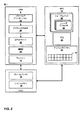
[0020] 図1は、本開示の1つまたは複数の態様を実施するように構成され得る例示的な計算デバイスを例示するブロック図である。図1に示されるように、計算デバイス2は、ビデオデバイス、メディアプレーヤ、セットトップボックス、モバイル電話およびいわゆるスマートフォンのようなワイヤレスハンドセット、携帯情報端末(PDAs)、デスクトップコンピュータ、ラップトップコンピュータ、ゲーミングコンソール、ビデオ会議ユニット、タブレット計算デバイス等を、限定されずに含む計算デバイスであり得る。図1の例では、計算デバイス2は、中央処理装置(CPU)6、システムメモリ10、およびGPU12を含み得る。計算デバイス2はまた、ディスプレイプロセッサ14、トランシーバモジュール3、ユーザインタフェース4、およびディスプレイ8を含み得る。トランシーバモジュール3およびディスプレイプロセッサ14は両方ともに、CPU6および/またはGPU12として同じ集積回路(IC)の一部であることができ、両方ともにCPU6および/またはGPU12を含むICまたは複数のICの外部に存在することができ、またはCPU6および/またはGPU12を含むICの外部に存在するICで形成され得る。
[0020] FIG. 1 is a block diagram illustrating an example computing device that may be configured to implement one or more aspects of the present disclosure. As shown in FIG. 1, the
[0021] 計算デバイス2は、明確さのために図1に示されない追加のモジュールまたはユニットを含み得る。例えば、計算デバイス2は、どちらも図1に示されない、スピーカおよびマイクロホンを、計算デバイス2がモバイルワイヤレス電話である例において、または計算デバイス2がメディアプレーヤであるスピーカにおいて電話通信を果たすために含み得る。計算デバイス2はまた、ビデオカメラを含み得る。さらに、図2に示される様々なモジュールおよびユニットは、計算デバイス2の全ての例において必要とは限らない。例えば、ユーザインタフェース4およびディスプレイ8は、計算デバイス2が、外部ユーザインタフェースまたはディスプレイとインタフェースするように装備されるデスクトップコンピュータまたは他のコンピュータである例において計算デバイス2の外部にあり得る。
[0021] The
[0022] ユーザインタフェース4の例は、トラックボール、マウス、キーボード、および他のタイプの入力デバイスを、限定されずに含む。ユーザインタフェース4は、タッチスクリーンであることもでき、ディスプレイ8の一部として組み込まれ得る。トランシーバモジュール3は、計算デバイス2と他のデバイスまたはネットワークとの間で無線または有線通信を可能にする回路を含み得る。トランシーバモジュール3は、変調器、復調器、増幅器、並びに有線または無線通信のための他のそうした回路を含み得る。
[0022] Examples of user interface 4 include, but are not limited to, a trackball, a mouse, a keyboard, and other types of input devices. The user interface 4 can also be a touch screen and can be incorporated as part of the display 8. The transceiver module 3 may include circuitry that enables wireless or wired communication between the
[0023] 図6は、実行のためにコンピュータプログラムの命令を処理するように構成される中央処理装置(CPU)のような、マイクロプロセッサであり得る。プロセッサ6は、計算デバイス2の動作を制御する汎用、または専用プロセッサを備え得る。ユーザは、1つまたは複数のソフトウェアアプリケーションをプロセッサ6に実行させるために計算デバイス2に入力を提供し得る。プロセッサ6上で実行するソフトウェアアプリケーションは、例えば、オペレーティングシステム、ワードプロセッサアプリケーション、電子メールアプリケーション、スプレッドシートアプリケーション、メディアプレーヤアプリケーション、ビデオゲームアプリケーション、グラフィカルユーザインタフェースアプリケーションまたは他のプログラムを含み得る。加えて、プロセッサ6は、GPU12の動作を制御するためにGPUドライバ22を実行し得る。ユーザは、キーボード、マウス、マイクロフォン、タッチパッドまたはユーザインタフェース4を介して計算デバイス2に結合される他の入力デバイスのような1つまたは複数の入力デバイス(図示されない)を介して入力を計算デバイス2に提供し得る。
[0023] FIG. 6 may be a microprocessor, such as a central processing unit (CPU) configured to process the instructions of a computer program for execution. The
[0024] プロセッサ6上で実行するソフトウェアアプリケーションは、ディスプレイ8に対するグラフィックスデータのレンダリングをプロセッサ6に命じる1つまたは複数のグラフィックスレンダリング命令を含み得る。いくつかの例において、ソフトウェア命令は、グラフィックスアプリケーションプログラミングインタフェース(API)、例えば、オープングラフィックスライブラリ(OpenGL(登録商標))API、オープングラフィックスライブラリ埋め込みシステム(Open Graphics Library Embedded Systems)(OpenGL ES)API、ダイレクト3D API、X3D API、RenderMan API、WebGL API、オープンコンピューティング言語(OpenCL(トレードマーク))または任意の他のパブリックまたは独自規格グラフィックスAPI等、に準拠し得る。グラフィックスレンダリング命令を処理するため、プロセッサ6は、1つまたは複数のグラフィックスレンダリングコマンドをGPU12に(例えば、GPUドライバ22を通して)発行してグラフィックスデータのレンダリングのいくつか、または全てをGPU12に行わせ得る。いくつかの例では、レンダリングされるべきグラフィックスデータが、例えば、点、線、三角形、四角形、トライアングルストライプなどのグラフィックス基本形状(graphics primitives)のリストを含み得る。
A software application executing on the
[0025] GPU12は、ディスプレイ8に1つまたは複数のグラフィックス基本形状をレンダリングするためのグラフィックス動作を行うように構成され得る。このため、プロセッサ6上で実行するソフトウェアアプリケーションのうちの1つがグラフィックス処理を要求するとき、プロセッサ6は、ディスプレイ8へのレンダリングのためにグラフィックスコマンドおよびグラフィックスデータをGPU12に提供し得る。グラフィックスデータは、例えば、描画コマンド(drawing commands)、ステート情報、プリミティブ情報(primitive information)、テクスチャ情報(texture information)等を含み得る。GPU12は、いくつかの例において、プロセッサ6に比べて複雑なグラフィック関連動作のより効率的な処理を提供する高度に並列な構造(highly-parallel structure)で構築され得る。例えば、GPU12は、並列方式で複数の頂点または画素について動作するように構成される、シェーダユニットのような、複数の処理要素を含み得る。GPU12の高度な並列性は、いくつかの例において、GPU12が、プロセッサ6を使用してディスプレイ8に直接シーンを描くより速くディスプレイ8上にグラフィックスイメージ(例えば、GUIsおよび2次元(2D)および/または3次元(3D)のグラフィックスシーン)を描くことを可能し得る。
The
[0026] GPU12は、いくつかの例において、計算デバイス2のマザーボードに統合され得る。他の例において、GPU12は、計算デバイス2のマザーボード内のポートにインストールされるグラフィックスカード上に存在するか、または、そうでなければ計算デバイス2と相互運用するように構成される周辺デバイス内に組み込まれ得る。GPU12は、1つまたは複数のマイクロプロセッサ、特定用途向け集積回路(ASICs)、フィールドプログラマブルゲートアレイ(FPGAs)、デジタルシグナルプロセッサ(DSPs)、または他の等価な集積またはディスクリート論理回路のような1つまたは複数のプロセッサを含み得る。GPU12はまた、1つまたは複数のプロセッサコアを含み得、GPU12はマルチコアプロセッサと称され得る。
[0026] The
[0027] グラフィックスメモリ40はGPU12の一部であり得る。このため、GPU12は、バスを使用せずに、グラフィックスメモリ40からデータを読み取り、グラフィックスメモリ40へデータを書き込み得る。言替えると、GPU12は、オフチップメモリの代わりに、ローカルストレージを使用してローカルにデータを処理し得る。このようなグラフィックスメモリ40は、オンチップメモリと称され得る。これは、重いバストラフィックを経験し得るバスを介してデータを読み書きGPU12の必要性を無くすことによる、より効率的な方式でGPU12が動作することを可能にする。グラフィックスメモリ40は、例えば、ランダムアクセスメモリ(RAM)、スタティックRAM(SRAM)、ダイナミックRAM(DRAM)、消去可能プログラマブルROM(EPROM)、電気的消去可能プログラマブルROM(EEPROM(登録商標))、フラッシュメモリ、磁気データ媒体または光学記憶媒体のような1つまたは複数の揮発性または不揮発性メモリ、または記憶デバイスを含み得る。
The
[0028] いくつかの例において、GPU12は、完全に形成された画像をシステムメモリ10に保存し得る。ディスプレイプロセッサ14は、システムメモリ10から画像を取り出して、ディスプレイ8の複数の画素に画像を表示するように照明させる値を出力し得る。ディスプレイ8は、GPU12によって生成された画像コンテンツを表示する計算デバイス2のディスプレイであり得る。ディスプレイ8は、液晶ディスプレイ(LCD)、有機発光ダイオードディスプレイ(OLED)、または陰極線管(CRT)ディスプレイ、プラズマディスプレイ、または他のタイプのディスプレイデバイスであり得る。
In some examples,
[0029] 図2は、さらに詳細に図1のプロセッサ6、GPU12、およびシステムメモリ10の例示的な実施形態を例示するブロック図である。図2に示すように、プロセッサ6は、各々1つまたは複数のソフトウェアアプリケーションまたはサービスである、少なくとも1つのソフトウェアアプリケーション18、グラフィックスAPI20、GPUドライバ22、およびメモリ管理ユニット(MMU)23を実行し得る。いくつかの例において、グラフィックスAPI20およびGPUドライバ22はCPU6のハードウェアユニットとして実施され得る。
[0029] FIG. 2 is a block diagram illustrating an exemplary embodiment of
[0030] プロセッサ6およびGPU12に利用可能なメモリは、システムメモリ10およびフレームバッファ16を含み得る。フレームバッファ16は、システムメモリ10の一部であり得、またはシステムメモリ10から分離され得る。フレームバッファ16は、レンダリングされた画像データを保存し得る。MMU23は、CPU6から、システムメモリ10またはグラフィックスメモリ40のようなメモリへのアクセスのための要求を扱うように構成されるハードウェアであり得る。例えば、MMU23はソフトウェアアプリケーション18からのメモリアクセス要求を扱い得る。MMU23は、こうしたメモリアクセス要求を扱うために1つまたは複数のページテーブルまたは翻訳ルックアサイドバッファ(TLBs: translation lookaside buffers)を使用して物理メモリアドレスへの仮想メモリアドレスの翻訳を行い得る。
The memory available for the
[0031] いくつかの例において、プロセッサ6は、レベル1(L1)キャッシュ、レベル2(L2)キャッシュ、レベル3(L3)キャッシュ、などの1つまたは複数のキャッシュ15を含む、または有し得る。1つまたは複数のキャッシュ15はシステムメモリ10に比べて速いメモリアクセスをプロセッサ6に提供し得、システムメモリ10の頻繁にアクセスされるメモリロケーションからのデータのコピーを保存し得る。
[0031] In some examples, the
[0032] ソフトウェアアプリケーション18は、GPU12の機能を利用する任意のアプリケーションであり得る。例えば、ソフトウェアアプリケーション18は、グラフィカルユーザインターフェース(GUI)アプリケーション、オペレーティングシステム、ポータブルマッピングアプリケーション、エンジニアリングまたは美術的アプリケーション(artistic applications)のためのコンピュータ支援設計プログラム(computer-aided design program)、ビデオゲームアプリケーション、または2Dまたは3Dグラフィックスを使用する他のタイプのソフトウェアアプリケーションであり得る。
The software application 18 can be any application that uses the function of the
[0033] ソフトウェアアプリケーション18は、GUIおよび/またはグラフィックスシーンをレンダリングするようにGPU12に命じる1つまたは複数の描画命令を含み得る。例えば、描画命令は、GPU12によってレンダリングされるべき1つまたは複数のグラフィックス基本形状のセットを定義する命令を含み得る。いくつかの例において、描画命令は、GUIで使用される複数のウィンドウイングサーフェス(windowing surfaces)の全てまたは一部を集合的に定義し得る。追加の例において、描画命令は、アプリケーションによって定義されるモデル空間またはワールド空間内で1つまたは複数のグラフィックスオブジェクトを含むグラフィックスシーンの全てまたは一部を集合的に定義し得る。
[0033] The software application 18 may include one or more drawing instructions that instruct the
[0034] ソフトウェアアプリケーション18は、1つまたは複数のグラフィックス基本形状をレンダリングして表示可能なグラフィックス画像にするためのGPU12への1つまたは複数のコマンドを発行するためにグラフィックスAPI20を介してGPUドライバ22を呼び出し得る。例えば、ソフトウェアアプリケーション18は、GPU12に基本形状定義(primitive definition)を提供するために、グラフィックスAPI20を介して、GPUドライバ22を呼び出し得る。いくつかの例において、基本形状は、例えば、三角形、四角形、扇形三角形(triangle fans)、または帯状連結三角形(triangle strips)等の描画基本形状のリストの形式でGPU12に提供され得る。基本形状定義は、レンダリングされるべき基本形状と関連する1つまたは複数の頂点を特定する頂点仕様(vertex specifications)を含み得る。頂点仕様は、各頂点についての位置座標(positional coordinates)と、いくつかの例において、頂点と関連する他の属性、例えば、カラー座標、法線ベクトル(normal vectors)、およびテクスチャ座標などと、を含み得る。基本形状定義はまた、基本形状タイプ情報(例えば、三角形、四角形、扇形三角形、帯状連結三角形等)、スケーリング情報、回転情報等も含み得る。
[0034] The software application 18 via the
[0035] ソフトウェアアプリケーション18によってGPUドライバ22に発行された命令に基づき、GPUドライバ22は、GPU12が基本形状をレンダリングするために行う1つまたは複数の動作を特定する1つまたは複数のコマンドを作成し(formulate)得る。GPU12がCPU6からのコマンドを受け取ると、グラフィックス処理パイプラインが、このコマンドを復号し、コマンドにおいて特定された動作を行うようにグラフィックス処理パイプラインを構成することをシェーダプロセッサ48上で実行し得る。例えば、グラフィックス処理パイプラインにおける入力アセンブラは、基本形状データを読み取ることができ、グラフィックス処理パイプラインにおける他のグラフィックスパイプラインステージによる使用のためにデータを基本形状にアセンブルし得る。特定された動作を行った後、グラフィックス処理パイプラインは、ディスプレイデバイスと関連するフレームバッファ16にレンダリングされたデータを出力する。
[0035] Based on instructions issued by the software application 18 to the
[0036] フレームバッファ16は、GPU12のための宛先画素(destination pixels)を保存する。各宛先画素は、一意的なスクリーン画素位置と関連し得る。いくつかの例において、フレームバッファ16は、カラーコンポーネントおよび各宛先画素のための宛先アルファ値(destination alpha value)を保存し得る。例えば、フレームバッファ16は、各画素のための赤、緑、青、アルファ(RGBA)を記憶し得、ここで「RGB」コンポーネントがカラー値に対応し、「A」コンポーネントが宛先アルファ値に対応する。フレームバッファ16およびメモリ10が別個のメモリユニットであるものとして例示されているが、他の例において、フレームバッファ16は、システムメモリ10の一部であり得る。
[0036] The
[0037] いくつかの例において、グラフィックス処理パイプラインが、1つまたは複数の頂点(vertex)シェーダステージ、ハル(hull)シェーダステージ、ドメイン(domain)シェーダステージ、ジオメトリ(geometry)シェーダステージ、および画素(pixel)シェーダステージを含み得る。グラフィックス処理パイプラインのこれらステージは考慮されたシェーダステージであり得る。これらのシェーダステージは、GPU12内の複数のシェーダユニット46上で実行する1つまたは複数のシェーダプログラムとして実施され得る。シェーダユニット46は、処理コンポーネントのプログラマブルパイプラインとして構成され得る。いくつかの例において、シェーディングユニット46は、「シェーダプロセッサ」、または「統合シェーダ(unified shaders)」と称されることができ、グラフィックスをレンダリングするためにジオメトリ、頂点、画素、または他のシェーディング動作を行い得る。シェーダユニット46は、各々がフェッチおよび復号動作のための1つまたは複数のコンポーネント、算術計算(arithmetic calculations)を行う1つまたは複数のALU、1つまたは複数のメモリ、キャッシュ、およびレジスタを含み得るシェーダプロセッサ48を含み得る。
[0037] In some examples, the graphics processing pipeline includes one or more vertex shader stages, a hull shader stage, a domain shader stage, a geometry shader stage, and A pixel shader stage may be included. These stages of the graphics processing pipeline can be considered shader stages. These shader stages may be implemented as one or more shader programs that execute on multiple shader units 46 within the
[0038] GPU12は、グラフィックス処理パイプラインにおける頂点シェーダステージ、ハルシェーダステージ、ドメインシェーダステージ、ジオメトリシェーダステージ、および画素シェーダステージのうちの1つまたは複数を実行するためにコマンドをシェーダユニット46に送ることによって、頂点シェーディング、ハルシェーディング、ドメインシェーディング、ジオメトリシェーディング、画素シェーディング等のような様々なシェーディング動作を行うようにシェーダユニット46を指定し得る。いくつかの例において、GPUドライバ22は、1つまたは複数のシェーダプログラムをコンパイルし、コンパイルされたシェーダプログラムをGPU12内に包含される1つまたは複数のプログラマブルシェーダユニット上にダウンロードするように構成され得る。シェーダプログラムは、例えば、OpenGLシェーディングランゲージ(GLSL)、ハイレベルシェーディングランゲージ(HLSL)、グラフィックスのためのC言語(C for Graphics)(Cg)シェーディングランゲージ等のような、ハイレベルシェーディングランゲージで書かれ得る。コンパイルされたシェーダプログラムは、GPU12内のシェーダユニット46の動作を制御する1つまたは複数の命令を含み得る。例えば、シェーダプログラムは、頂点シェーダステージの機能を行うためにシェーダユニット46によって実行され得る頂点シェーダプログラム、ハルシェーダステージの機能を行うためにシェーダユニット46によって実行され得るハルシェーダプログラム、ドメインシェーダステージの機能を行うためにシェーダユニット46によって実行され得るドメインシェーダプログラム、ジオメトリシェーダステージの機能を行うためにシェーダユニット46によって実行され得るジオメトリシェーダプログラム、および/または画素シェーダの機能を行うためにシェーダユニット46によって実行され得る画素シェーダプログラムを含み得る。頂点シェーダプログラムは、プログラマブル頂点シェーダユニット、または統合されたシェーダユニットの実行を制御でき、1つまたは複数の頂点単位の動作を特定する命令を含み得る。
[0039] グラフィックスメモリ40は、GPU12の集積回路に物理的に統合されたオンチップ記憶装置、またはメモリを含み得る。グラフィックスメモリ40がオンチップである場合、GPU12は、システムバスを介してシステムメモリ10から値を読み取ること、またはシステムメモリ10に値を書き込むことより速くグラフィックスメモリ40から値を読み取り、またはグラフィックスメモリ40に値を書き込むことが可能であり得る。
[0038] The
[0039] The
[0040] GPU12はまた、透過的フォーマット変換器(TFC)24を含み得る。TFC24は、CPU6または任意の他の処理コアをイネーブルするハードウェアであり得、グラフィックスメモリ40に保存された画素データ41に従う画素フォーマットをサポートしない任意の他の処理コアがあたかもCPU6によってサポートされた画素フォーマットに従ってグラフィックスメモリ40に保存された画素データ41を見るようにする。イネーブルするハードウェアであり得る。
言替えると、CPU6は、TFC24を通じて、グラフィックスメモリ40に保存された画素データを、それがサポートする画素フォーマットで読み書き可能である。例えば、画素データがグラフィックスメモリ40にタイル画素フォーマットで保存される場合であって、CPU6がNV12のような線形画素フォーマットをサポートする場合に、TFC24は、画素データ41がCPU6によってサポートされるNV12のような線形フォーマットで整列されてCPU6に現れるようにして、画素データ41の線形ベースビューをCPU6に提供し得る。TFC24は、CPU6によってサポートされる画素フォーマットに従う画素データ41に対するCPU6によるどの書き込みもそれがグラフィックメモリ40に保存されるフォーマットに戻すように翻訳し得る。このため、TFC24は、画素データ41がCPU6によってサポートされる画素フォーマットにあったかのように画素データ41を扱うことをCPU6にイネーブルして、画素データ41がCPU6によってサポートされない画素フォーマットでグラフィックスメモリ40に保存される一方でCPU6が画素データ41をCPU6によってサポートされる画素フォーマットに従って読み書きできるようにする。
[0040] The
In other words, the
[0041] 本開示の態様に従って、TFC24はグラフィックスメモリ40に保存された画素データ41に関する、CPU6による要求が第1のデータフォーマットにある画素データ41に関する要求を示すものであると決定し得る。TFC24は、グラフィックスメモリ40における画素データ41に関する要求に少なくとも一部基づいて、第2のデータフォーマットにある画素データ41をグラフィックスメモリ40から取得し得る。TFC24は、取得された画素データ41を第2のデータフォーマットから第1のデータフォーマットへ変換し得る。TFC24は、第1のデータフォーマットにある変換された画素データ41を、プロセッサ6によってアクセス可能であるキャッシュのようなメモリに保存し得る。
[0041] In accordance with aspects of the present disclosure,
[0042] いくつかの例において、TFC24はGPU12に含まれる特定のハードウェアロジックであり得る。いくつかの他の例において、TFC24はシェーダユニット46のシェーダプロセッサ48によって実行されるシェーダコードを含み得る。他の例において、TFC24は計算デバイス2に含まれるものの、厳密にはGPU12に含まれない特定のハードウェアロジックであり得る。例えば、TFC24はCPU6に組み込まれ得るか、またはCPU6およびGPU12から分離された独立型ハードウェアコンポーネントであり得る。
[0042] In some examples, the
[0043] 図3は、図2のTFC24の例示的な機能を例示するブロック図である。図3に示すように、グラフィックスメモリ40は、タイルベース画素フォーマットに従う画素データ41を保存し得る。プロセッサ26は、タイルベース画素フォーマットからの読み取りおよびタイルベース画素フォーマットへの書き込みのできない処理コアであり得る。例えば、プロセッサ26は線形画素フォーマットをサポートし得るものの、タイルベース画素フォーマットをサポートし得ない。プロセッサ26が画素データ41に対して読み書きすることをイネーブルするために、TFC24は、どのように画素データ41がグラフィックスメモリ40に保存されているかとは無関係(independent)のプロセッサ26にグラフィックスメモリ40に保存された画素データ41のビュー43を提供し得る。ビュー43はプロセッサ26によってサポートされる画素フォーマットにある画素データ41を表し、プロセッサ26の視点から、グラフィックスデータがプロセッサ26のサポートする、YUV、NV1、および同等なもののような画素フォーマットに従ってビュー43でレイアウトされるようにし得る。TFC24はそれゆえ、画素データ41がグラフィックスメモリ40に保存されるかのように、プロセッサ26が画素データ41に対してよみ書きをすることをイネーブルし得る。TFC24はプロセッサ26から読出および書込要求を受けることができ、これら読出および書込要求を画素データ41のタイルベース画素フォーマットのための適切な読出および書込要求に翻訳できる。
[0043] FIG. 3 is a block diagram illustrating exemplary functions of the
[0044] プロセッサ26にビュー43を提示するTFC24は、プロセッサ26に色アパチャ(colored aperture)を提示することを含み得る。色アパチャは、特定のターゲット画素フォーマットで物理メモリをアクセスするために使用できる、物理的および/または仮想のうちのどちらかのアドレス範囲であり得る。例えば、TFC24は、プロセッサ26によってサポートされる画素フォーマットにある画素データ41をアクセスするためにプロセッサ26がメモリアクセスし得る仮想アドレス範囲をプロセッサ26に提示し得る。TFC24は、プロセッサ26が色アパチャを読み出しまたは書き込みをしようとしているとTFC24が決定した場合に、プロセッサ26からのメモリ要求の仮想アドレスに基づいて、プロセッサ26によってサポートされる画素フォーマットにある画素データ41からの読み出しまたはへの書き込みをプロセッサ26がしようとしていると決定可能であり得る。複数の異なるソフトウェアアプリケーションおよび/または異なるプロセッサが画素データ41へのアクセスを要求する場合、TFC24が重複しない異なるソフトウェアアプリケーションおよび/または異なるプロセッサの各々ために一意の色アパチャを提供し得る。このようにして、TFC24は要求しているソフトウェアアプリケーションおよび/またはプロセッサを、これらソフトウェアアプリケーションおよび/またはプロセッサからの画素データ41に関するアクセスのための要求に含まれた仮想アドレスに少なくとも一部基づいてこれらソフトウェアアプリケーションおよび/またはプロセッサによってサポートされる画素フォーマットと共に決定することが可能であり得る。
[0044] The
[0045] 図4は、図2のTFC24の例示的な実施形態を例示するブロック図である。図4に示すように、プロセッサ50Aおよびプロセッサ50Bは各々グラフィックスメモリ40に保存された画素データ41に対するアクセスを要求し得る。プロセッサ50Aがアクセスを要求しているグラフィックスメモリ40に保存された画素データの基底画素フォーマットをプロセッサ50Aがサポートしないかまたはその知識を持たない一方で、プロセッサ50Bがアクセスを要求しているグラフィックメモリ40に保存された画素データ41の基底画素フォーマットをサポートするおよび/またはその知識を持ち得る。プロセッサ50Aの例は、CPU6を、グラフィックスメモリ40に保存された画素データ41の画素フォーマットをサポートしないか、またはその知識を持たない任意の他の処理ハードウェアと共に含み得る。より具体的には、プロセッサ50AがCPU6である場合に、CPU6上で実行するソフトウェアアプリケーション18がグラフィックスメモリ40に保存された画素データに対するアクセスを要求し得る。プロセッサ50Bの例は、GPU12、シェーダプロセッサ48、ビデオエンコーダ、複数のビデオデコーダ、ディスプレイプロセッサ、ディスプレイ、デジタル信号プロセッサ(DPSs)、カメラプロセッサ、ビデオプロセッサ、およびグラフィックスメモリ40に保存された画素データの画素フォーマットをサポートするおよび/またはその知識をもつようなものを含み得る。
[0045] FIG. 4 is a block diagram illustrating an exemplary embodiment of
[0046] プロセッサ50Aおよび50Bは各々グラフィックスメモリ40に保存された画素データ41に対するアクセスを要求し得る。上で論じたように、プロセッサ50Aおよび50Bがアクセスを要求する画素データ41は、プロセッサ50Bによってサポートされるもののプロセッサ50Aによってサポートされない特定の画素フォーマットに従って配列され得る。
[0046]
[0047] プロセッサ50Aは仮想アドレス51Aからデータに関する要求をでき、プロセッサ50Bは仮想アドレス51Bからデータに関する要求をできる。MMU52Aは、プロセッサ50Aからのデータに関する要求を扱って仮想アドレス51Aを翻訳されたアドレス53に変換するためにページテーブル54Aを使用し得る。例えば、プロセッサ50AがCPU6である場合に、MMU52AがMMU23であり得る。MMU52Aは仮想アドレス51Aを、1つまたは複数のカラービットを仮想アドレス51Aの前に添付することを含む翻訳されたアドレス53に変換し、翻訳されたアドレス53の1つまたは複数の上位ビットが仮想アドレス51を続けた1つまたは複数のカラービットを含むようにし得る。カラービットはプロセッサ50Aによってサポートされる画素フォーマットをTFC24へインジケートし得る。例えば、64ビットアドレス可能空間において、仮想アドレス51Aは全64ビットをとり得ない。このため、MMU52Aは64ビット以下の翻訳アドレス53を生成するために1つまたは複数のカラービットを仮想アドレスに連結可能であり得る。同様に、MMU52Bは、プロセッサ50Bからのデータに関する要求を扱い、仮想アドレス51Bを使用して物理アドレス55Bを調べるためにページテーブル54Bを使用し得る。プロセッサ50Bはピクセルデータ41がグラフィックスメモリ40に保存された画素フォーマットをサポートすることから、MMU52は、仮想アドレス51Bを翻訳されたアドレスに翻訳する代わりに、グラフィックスメモリ40における要求されたデータの物理アドレスである物理アドレス55Bへ仮想アドレス51Bを直接的に翻訳できる。
The
[0048] TFC24は、翻訳されたアドレス53を受け取ることができ、ページテーブル56へインデックスするための翻訳アドレス53を使用することに少なくとも一部基づいて、プロセッサ50Aによって要求されたグラフィックスメモリ40における画素データ41のロケーションをインジケートする物理アドレス55Aを決定できる。TFCは、少なくとも物理アドレス55Aに一部基づいてグラフィックスメモリ40における画素データ41を取得でき、取得された画素データ41を、画素データ41がそれに従ってグラフィックスメモリ40に保存された画素フォーマットから、プロセッサ50Aによってサポートされる画素フォーマットに翻訳できる。取得された画素データ41を翻訳することは、画素データ41を圧縮解除して、プロセッサ50A等によってサポートされる画素フォーマットに従って画素情報を再編成することを含み得る。TFC24は、変換された画素データ41をプロセッサ50A内の1つまたは複数のキャッシュ(例えば、1つまたは複数のキャッシュ15)に保存することなどで、変換された画素データ41をプロセッサ50Aに戻し得る。
[0048] The
[0049] プロセッサ50Aは、プロセッサ50Aによってサポートされる画素フォーマットに従ってその1つまたは複数のキャッシュに保存された画素データ41に対して読み書きし得る。プロセッサ50Aがその1つまたは複数のキャッシュフラッシュから画素データ41を追い出したときである、キャッシュフラッシュに応答して、TFC24は仮想アドレス51Aに少なくとも一部基づいて翻訳されたものである、翻訳されたアドレス53と一緒にプロセッサ50Aから画素データ41を受け取り得る。TFC24は画素データ41をグラフィックスメモリ40にそれが保存される画素フォーマットに戻るように変換でき、画素データ41がグラフィックスメモリ40に保存される画素フォーマットに画素情報を再編成すること、および画素データ41がグラフィックスメモリ40に保存される画素フォーマットに従って画素情報を圧縮することを含む。TFC24はまた、翻訳されたアドレス53をページテーブル56を使用して物理アドレス55Aに変換でき、物理アドレス55Aで画素データ41をグラフィックスメモリ40に保存できる。
[0049] The
[0050] 図5は、図4の翻訳されたアドレス53の例示的なフォーマットを例示するブロック図である。図5に示すように、翻訳されたアドレス53は、画素データ41へのアクセスを要求しているプロセッサを識別する1つまたは複数の上位ビットと共にこのプロセッサによってサポートされた1つまたは複数の画素フォーマットを含み得る。翻訳されたアドレス53は、仮想アドレス51に連結された1つまたは複数の上位ビットを含み得る。一例において、翻訳されたアドレス53の1つまたは複数の最上位ビットはカラービット57を含み得る。カラービット57は、要求しているプロセッサによってサポートされた画素フォーマットを特定する1つまたは複数のビットであり得る。他の例において、翻訳されたアドレス53の1つまたは複数の最上位ビットは、要求しているプロセッサを識別するマスターID58と共に、翻訳されたアドレス53の最上位ビットが1である場合に1にセットされるビット59を含み得る。他の例において、翻訳されたアドレス53の1つまたは複数の最上位ビットは、同様のアクセス許可を持つ複数のプロセッサのグループ内にあるものとして要求しているプロセッサを識別する仮想マシンID60と共に、翻訳されたアドレス53の最上位ビットが1である場合に1にセットされるビット61を含み得る。
[0050] FIG. 5 is a block diagram illustrating an exemplary format of translated
[0051] 図6は、図2のTFC24の例示的実施形態を例示するプロック図である。図5に示すように、TFC24は、タグデコーダ66、翻訳ルックアサイドバッファ(TLB)68、パッキングユニット69A−69N、(「パッキングユニット69」)、およびアドレス計算ユニット67を含み得る。TFC24はまた、メタデータサーバ64およびハードウェアテーブルウォーカ(HTW)サーバ62を含み得る。
[0051] FIG. 6 is a block diagram illustrating an exemplary embodiment of
[0052] 上で論じたように、TFC24は、翻訳されたアドレス53を物理アドレス55Aに翻訳し得る。TFCはまた、プロセッサによってサポートされた画素フォーマットと、グラフィックメモリ40に保存された画素データ41の画素フォーマットとの間の変換をし得る。タグデコーダ66は、翻訳されたアドレス53を復号して、グラフィックスメモリ40における画素データ41をアクセスすることを試みている処理コア(例えば、プロセッサ50A)によってサポートされた画素フォーマットのような、翻訳されたアドレスに含まれる情報を決定すし得る。
[0052] As discussed above,
[0053] メタデータサーバ64は、TFC24によって受け取った、翻訳されたアドレス53のために1つまたは複数のビュー定義を決定し得る。翻訳されたアドレス53のためのビュー定義は、画素データ41に関する要求を送ったプロセッサ50Aに関する情報と共に、翻訳されたアドレス53を介して要求された画素データ41に関する情報を含み得る。1つまたは複数のビュー定義は、要求された画素データ41のステータス、要求された画素データ41の開始アドレス、要求された画素データ41の長さ、要求しているプロセッサ50Aによってサポートされたターゲット画素フォーマット、要求された画素データ41のタイル幅およタイル長、要求された画素データ41のストライド(stride)、等と共に、画素データ41を要求しているプロセッサ50Aによってサポートされる画素フォーマットに変換するために必要であり得る任意の他の必要データを含み得る。いくつかの例において、メタデータサーバ64は、それが受け取る、翻訳されたアドレス53毎の1つまたは複数のビュー定義を含み得る。
[0053] The
[0054] アドレス計算ユニット67は、翻訳されたアドレス53から物理アドレス55Aを決定し得る。TLB68は、物理アドレス翻訳に対する1つまたは複数の翻訳されたアドレスをキャッシュし得る。アドレス計算ユニット67は、TLB68が翻訳されたアドレス53の物理アドレス55Aをキャッシュしたかどうか決定するためにTLB68に問い合わせ得る。TLB68が翻訳されたアドレス53の物理アドレス55Aをキャッシュしていれば、TFC24がメタデータサーバ64によって提供された画素データ41のためのビュー定義に基づいて物理アドレス55Aで画素データ41をアクセスし得る。
[0054] The address calculation unit 67 may determine the
[0055] TLB68が翻訳されたアドレス53の物理アドレス55Aをキャッシュしていなければ、アドレス計算ユニット67が翻訳されたアドレス53のカラービットをはがし(strip)得、このはがされた翻訳されたアドレスを翻訳されたアドレス53の物理アドレスを決定するためにHTWサーバ62へ提供し得る。HTWサーバ62は、1つまたは複数のページテーブル(例えば、ページテーブル54Aおよび/またはページテープル56)をアクセスし、翻訳されたアドレス53の物理アドレス55Aを決定するためのハードウェアであり得る。HTWサーバ62が翻訳されたアドレス53の物理アドレス55Aを決定することに応答して、TFC24はメタデータサーバ64によって提供された画素データ41のためのビュー定義に基づいて物理アドレス55Aで画素データ41をアクセスし得る。
[0055] If the
[0056] パッキングユニット69は、要求している処理コアによってサポートされた画素フォーマットと、グラフィックスメモリ40に保存された画素データ41の画素フォーマットとの間の翻訳をし得る。パッキングユニット69は、画素フォーマット間で変換するためにカラー変換、タイル貼り、タイルはがし、圧縮、圧縮解除、等を行い得る。いくつかの例において、パッキングユニット69は固定の機能ハードウェアを含み得る。他の例において、パッキングユニット69の機能は、GPU12、シェーダユニット46、専用デジタル信号プロセッサ、等を介するような他の手段で実施され得る。いくつかの例において、TFC24の全機能は、シェーダユニット46上で実行するシェーダコードで実施され得る。
[0056] The packing unit 69 may translate between the pixel format supported by the requesting processing core and the pixel format of the
[0057] 図7は、例示的な仮想アドレスを例示的な物理アドレスに翻訳するために2レベルページテーブルマッピングを利用する図2のTFC24を例示するブロック図である。単一レベルページテーブルは概ね高レベルオペレーティングシステム(HLOS)によって管理され得ることから、2レベルページテーブルはTFC24がアドレスの翻訳および画素フォーマットの変換をHLOSから隠すことをイネーブルし、MMUが単一ページテーブルを使用して仮想アドレスを物理アドレスに単純に翻訳することにHLOSに見えるようにできる。
[0057] FIG. 7 is a block diagram illustrating the
[0058] 図7に示すように、MMU52Aは、ページテーブル70およびページテーブル72を備える2ステージページテーブルを利用する2レベルMMUであり得る。HLOSは、ハイパーバイザーまたは仮想マシンモニタ(VMM)がページテーブル72を管理し得る一方でページテーブル70を管理し得る。上で論じたように、ハイパーバイザーまたはVMMがページテーブル72を使用して第2のステージマッピングを管理し得ることから、こうした第2のレベルマッピングがHLOSから隠され得る。
As shown in FIG. 7, the
[0059] ページテーブル70および72は、ソフトウェアアプリケーション18が画素フォーマット変換のためにノーマルページをマッピング可能であり得る場合に専用メモリセグメントを有し得る。MMU52Aはまた、ページテーブル70および72を使用してユーザアドレス空間およびカーネルアドレス空間を管理し得る。ユーザアドレス空間は、カーネルアドレス空間がカーネルのような低レベル特権コードによってアクセス可能であり得る一方で、HLOS上で稼働しているソフトウェアアプリケーションによってアクセス可能であり得る。こうして、カーネルアドレス空間は無特権ソフトウェアアプリケーションによるアクセスから保護され得る。ページテーブル70および72は、ユーザアドレス空間仮想アドレスを翻訳するためのユーザアドレス空間部分74およびカーネルアドレス空間仮想アドレスを翻訳するためのカーネルアドレス空間部分76を含み得る。
[0059] The page tables 70 and 72 may have dedicated memory segments if the software application 18 may be able to map normal pages for pixel format conversion.
[0060] 図7の例において、仮想アドレス51Aは、ユーザアドレス空間にあり得る0x7800であり得る。MMU52Aは、ページテーブル70へインデックスするための仮想アドレス51Aを利用して、仮想アドレス51Aを0xabcdの中間物理アドレス(intermediate physical address)71へ翻訳し得る。IPA71は、カラービット57のようなカラービットに連結された仮想アドレス51Aであり得、MMU52Aはページテーブル72へインデックスするためのIPAを使用して、中間物理アドレス71を0x1002000の中間物理アドレス73へ翻訳し得る。IPA73は、その1つまたは複数の最上位ビットにあるIPA71のカラービットに保持され得る。中間物理アドレス73は、図4の変換されたアドレス53と同じであり得る。
[0060] In the example of FIG. 7, the
[0061] TFC24は、0x1002000の物理アドレス73からカラービット0x1000000をはがし、物理アドレス55Aを決定するために結果のアドレス0x2000をHTWサーバ62に提供し得る。結果のアドレス0x2000はカーネルアドレス空間にあり得ることから、HTWサーバ62は、結果のアドレス0x2000を利用して、ページテーブル72のカーネルアドレス空間部分76へインデックスして、0xceedのアドレスをもたらし得る。HTWサーバ62は、さらにページテーブル72のカーネルアドレス空間部分76へインデックスするために0xceedのアドレスを利用して0x0800の物理アドレス55Aをもたらし得る。HTWサーバ62は、0x0800の物理アドレス55AをTFC24に提供でき、TFCは0x0800の物理アドレス55Aでグラフィックスメモリ40をアクセスできる。こうして、ページテーブル70および72のカーネルアドレス空間部分76は図4のページテーブル56の役を務め得る。
[0061] The
[0062] 物理アドレス55Aを決定するためにページテーブル70および72のカーネルアドレス空間およびカーネルアドレス空間部分76を利用することによって、TFC24はCPU6のようなプロセッサによって課せされたセキュリティ体制を使用して物理アドレス55Aへの仮想アドレス51Aの翻訳を行い得る。このセキュリティ体制はまた、複数のソフトウェアアプリケーションおよび/または複数の処理コアのための複数のカラーアパチャを生成することにおいてTFC24をメモリ効率的にできる。
[0062] By utilizing the kernel address space and kernel
[0063] 図8は、透過的に画素フォーマットを変換するためのプロセスを例示するフローチャートである。図8に示すように、このプロセスは、第1のデータバッファに保存されたデータに関する、少なくとも1つのプロセッサによる要求が第1のデータフォーマットにあるこのデータに関する要求を示すものであると、TFC24によって、決定すること(102)を含み得る。方法は、第1のデータバッファに保存されたデータに関する要求に少なくとも一部基づいて、第2のデータフォーマットにあるこのデータを第1のデータバッファから、TFC24によって、取得すること(104)をさらに含み得る。方法は、取得されたデータを第2のデータフォーマットから第1のデータフォーマットへ、TFC24によって、変換すること(106)をさらに含み得る。方法は、第1のデータフォーマットにある変換されたデータを、少なくとも1つのプロセッサによってアクセス可能である第2のデータバッファに、TFC24によって、保存すること(108)をさらに含み得る。
[0063] FIG. 8 is a flowchart illustrating a process for transparently converting a pixel format. As shown in FIG. 8, this process is performed by the
[0064] いくつかの例において、第1のデータバッファに保存されたデータに関する、少なくとも1つのプロセッサによる要求が、仮想アドレス51Aで保存されたデータに関する要求を含み、第2のデータフォーマットにあるこのデータを第1のデータバッファから、TFC24によって、取得することは、第2のデータフォーマットにあるこのデータを仮想アドレスに対応する物理アドレスで第1のデータバッファから、TFC24によって、取得することをさらに備える。いくつかの例において、プロセスは仮想アドレス51Aに少なくとも一部基づき、翻訳されたアドレス53をMMU52Aによって、決定することと、翻訳されたアドレス53に少なくとも一部基づいて、物理アドレス55AをTFC24によって、決定することとをさらに含む。
[0064] In some examples, the request by the at least one processor for data stored in the first data buffer includes a request for data stored at the
[0065] いくつかの例において、翻訳されたアドレス53の1つまたは複数の最上位ビットは、1つまたは複数のカラービットを備え、ここにおいて1つまたは複数のカラービットは1つまたは複数のプロセッサによってサポートされた少なくとも画素フォーマットをインジケートする。いくつかの例において、翻訳されたアドレス53を決定することは、仮想アドレス51Aに少なくとも一部基づいて1つまたは複数のカラービットを、MMU52Aによって、決定することをさらに含む。いくつかの例において、プロセスは、仮想アドレス51Aに少なくとも一部基づいて、第1のレベルページテーブル70を使用するMMU52Aによって、中間物理アドレス71を決定することと、中間物理アドレス71に少なくとも一部基づいて、第2のレベルページテーブル72を使用するMMU52Aによって、翻訳されたアドレス53を決定することとをさらに含む。いくつかの例において、翻訳されたアドレス53に少なくとも一部基づいて物理アドレス55Aを、TFC24によって、決定することは、1つまたは複数のページテーブル70および72のカーネルアドレス空間部分76に少なくとも一部基づいて物理アドレス55Aを、TFC24によって、決定することさらに含む。
[0065] In some examples, the one or more most significant bits of the translated
[0066] いくつかの例において、第2のデータバッファは、少なくとも1つのプロセッサのためにキャッシュを備える。いくつかの例において、データは画素データ41を備え、第1のデータフォーマットは第1の画素フォーマットを備え、第2のデータフォーマットは第2の画素フォーマットを備える。いくつかの例において、プロセスは、第1のデータフォーマットにある第2のデータを少なくとも1つのプロセッサから、TFC24によって、受け取ることと、第2のデータを第1のデータフォーマットから第2のデータフォーマットへ、TFC24によって、変換することと、第2のデータフォーマットにある、変換されたデータを第1のデータバッファに、TFC24によって、保存することとをさらに含む。
[0066] In some examples, the second data buffer comprises a cache for at least one processor. In some examples, the data comprises
[0067] 1つまたは複数の例において、記載された機能は、ハードウェア、ソフトウェア、ファ−ムウェア、またはそれらの任意の組合せに実施され得る。ソフトウェアで実施される場合、機能は、コンピュータ可読媒体上における1つまたは複数の命令またはコードとして記憶または送信され得る。コンピュータ読取可能媒体は、1つの場所から別の場所へのコンピュータプログラムの転送を容易にする任意の媒体を含む通信媒体またはコンピュータデータ記憶媒体を含みうる。データ記憶媒体は、本開示内で説明された技法の実施形態のための命令、コード、および/またはデータ構造を取り出すために、1つまたは複数のコンピュータまたは1つまたは複数のプロセッサによってアクセスされることができる任意の利用可能な媒体であり得る。限定ではなく例として、そのようなコンピュータ可読媒体は、RAM、ROM、EEPROM、CD−ROMまたは他の光学ディスク記憶装置、磁気ディスク記憶装置または他の磁気記憶デバイス、あるいは命令またはデータ構造の形式で所望のプログラムコードを搬送または記憶するよう使用されることができ、コンピュータによってアクセスされることができる任意の他の媒体を備えることができる。また、任意の接続は、厳密にはコンピュータ可読媒体と称される。例えば、ソフトウェアがウェブサイト、サーバ、または他の遠隔ソースから、同軸ケーブル、光ファイバーケーブル、ツイストペア、デジタル加入者回線(DSL)、あるいは赤外線、無線、およびマイクロ波のようなワイヤレス技法を使用して送信される場合、同軸ケーブル、光ファイバーケーブル、ツイストペア、DSL、あるいは赤外線、無線、およびマイクロ波のようなワイヤレス技法は送信媒体の定義に含まれている。ディスク(disk)およびディスク(disc)は、本明細書で使用される場合、コンパクトディスク(CD)(disc)、レーザーディスク(登録商標)(disc)、光ディスク(disc)、デジタル多用途ディスク(DVD)(disc)、フロッピー(登録商標)ディスク(disk)およびBlu−ray(登録商標)ディスク(disc)を含み、ここで、ディスク(disk)は通常、磁気的にデータを再生し、その一方でディスク(disc)は、レーザーを用いて光学的にデータを再生する。上記の組み合わせはまた、コンピュータ可読媒体の範疇に含まれるべきである。 [0067] In one or more examples, the functions described may be implemented in hardware, software, firmware, or any combination thereof. If implemented in software, the functions may be stored on or transmitted over as one or more instructions or code on a computer-readable medium. Computer-readable media can include communication media or computer data storage media including any medium that facilitates transfer of a computer program from one place to another. A data storage medium is accessed by one or more computers or one or more processors to retrieve instructions, code, and / or data structures for embodiments of the techniques described within this disclosure. It can be any available medium that can. By way of example, and not limitation, such computer readable media is in the form of RAM, ROM, EEPROM, CD-ROM or other optical disk storage, magnetic disk storage or other magnetic storage device, or instructions or data structures. Any other medium that can be used to carry or store the desired program code and that can be accessed by a computer can be provided. Also, any connection is strictly referred to as a computer readable medium. For example, software transmits from a website, server, or other remote source using coaxial cable, fiber optic cable, twisted pair, digital subscriber line (DSL), or wireless techniques such as infrared, wireless, and microwave Where applicable, coaxial cable, fiber optic cable, twisted pair, DSL, or wireless techniques such as infrared, radio, and microwave are included in the definition of transmission media. Disc and disc as used herein are compact disc (CD), laser disc (registered trademark), optical disc (disc), digital versatile disc (DVD) ) (Disc), floppy (R) disk and Blu-ray (R) disk, where the disk normally reproduces data magnetically while A disc optically reproduces data using a laser. Combinations of the above should also be included within the scope of computer-readable media.
[0068] コードは、1つまたは複数の1デジタルシグナルプロセッサ(DSPs)、汎用マイクロプロセッサ、特定用途向け集積回路(ASICs)、フィールドプログラマブル論理アレイ(FPGAs)、または他の同等な集積またはディスクリートな論理回路等の、1つまたは複数のプロセッサによって実行され得る。従って、本開示で使用される場合、「プロセッサ」および「処理ユニット/処理装置」という用語は、前述の構造、または本開示に説明される技法の実施形態に適した任意の他の構造のいずれかを指し得る。加えて、いくつかの態様では、本開示に説明される機能は、符号化および復号のために構成された専用ハードウェアおよび/またはソフトウェアモジュール内で提供され得る、あるいは組み合わせられたコーデック内に組み込まれ得る。また、技法は、1つまたは複数の回路または論理要素で完全に実施され得る。
[0069] 本開示の技法は、ワイヤレスハンドセット、集積回路(IC)またはICsのセット(例えば、チップセット)を含む、幅広い様々なデバイスまたは装置で実施され得る。様々なコンポーネント、モジュール、またはユニットは、開示された技法を行うように構成されるデバイスの機能的な態様を強調するように本開示において説明されるが、必ずしも異なるハードウェアユニットによる実現を必要としない。むしろ、上に説明されたように、様々なユニットは、コーデックハードウェアユニットに組み合わされ得るか、または適切なソフトウェアおよび/またはファームウェアと併せて、上に説明されたような1つまたは複数のプロセッサを含む、相互運用のハードウェアユニット(interoperative hardware units)の集合によって提供され得る。
[0068] The code may be one or more digital signal processors (DSPs), general purpose microprocessors, application specific integrated circuits (ASICs), field programmable logic arrays (FPGAs), or other equivalent integrated or discrete logic. It may be executed by one or more processors, such as a circuit. Thus, as used in this disclosure, the terms “processor” and “processing unit / processing device” refer to either the foregoing structure or any other structure suitable for embodiments of the techniques described in this disclosure. Can point to. In addition, in some aspects, the functions described in this disclosure may be provided in dedicated hardware and / or software modules configured for encoding and decoding, or incorporated in a combined codec. Can be. Also, the techniques may be fully implemented with one or more circuits or logic elements.
[0069] The techniques of this disclosure may be implemented in a wide variety of devices or apparatuses, including wireless handsets, integrated circuits (ICs) or sets of ICs (eg, chip sets). Various components, modules, or units are described in this disclosure to emphasize the functional aspects of a device that is configured to perform the disclosed techniques, but need not necessarily be implemented by different hardware units. do not do. Rather, as described above, the various units may be combined into a codec hardware unit or one or more processors as described above in conjunction with appropriate software and / or firmware. Can be provided by a set of interoperable hardware units.
[0070] 本開示の様々な態様が説明されてきた。これらおよび他の態様は、特許請求の範囲の範疇にある。
以下に本願の出願当初の特許請求の範囲に記載された発明を付記する。
[C1] 画素処理のための方法であって、
第1のデータバッファに保存されたデータに関する、少なくとも1つのプロセッサによる要求が第1のデータフォーマットにある前記データに関する要求を示すものであると、透過的フォーマット変換器(TFC)によって、決定することと、
前記第1のデータバッファに保存されたデータに関する前記要求に少なくとも一部基づいて、第2のデータフォーマットにある前記データを前記第1のデータバッファから、前記TFCによって、取得することと、
前記取得されたデータを前記第2のデータフォーマットから前記第1のデータフォーマットへ、前記TFCによって、変換することと、
前記第1のデータフォーマットにある前記変換されたデータを、前記少なくとも1つのプロセッサによってアクセス可能である第2のデータバッファに、前記TFCによって、保存することと
を備える、方法。
[C2] 前記第1のデータバッファに保存されたデータに関する、前記少なくとも1つのプロセッサによる前記要求は、仮想アドレスに保存されたデータに関する要求を備え、
前記第2のデータフォーマットにある前記データを前記第1のデータバッファから、前記TFCによって、取得することは、前記第2のデータフォーマットにある前記データを、前記仮想アドレスに対応する物理アドレスで前記第1のデータバッファから、前記TFCによって、取得することをさらに備える、C1に記載の方法。
[C3] 前記仮想アドレスに少なくとも一部基づいて翻訳されたアドレスを、メモリ管理ユニット(MMU)によって、決定することと、
前記翻訳されたアドレスに少なくとも一部基づいて前記物理アドレスを、前記TFCによって、決定することと
をさらに備える、C2に記載の方法。
[C4] 前記翻訳されたアドレスの1つまたは複数の最上位ビットは1つまたは複数のカラービットを備え、前記1つまたは複数のカラービットは前記1つまたは複数のプロセッサによってサポートされた少なくとも画素フォーマットをインジケートする、C3に記載の方法。
[C5] 前記翻訳されたアドレスを決定することは、前記仮想アドレスに少なくとも一部基づいて前記1つまたは複数のカラービットを、MMUによって、決定することをさらに備える、C3に記載の方法。
[C6] 前記仮想アドレスに少なくとも一部基づいて中間物理アドレスを、第1のレベルページテーブルを使用するMMUによって、決定することと、
前記中間物理アドレスに少なくとも一部基づいて前記翻訳されたアドレスを、第2のレベルページテーブルを使用するMMUによって、決定することとをさらに備える、C3に記載の方法。
[C7] 前記翻訳されたアドレスに少なくとも一部基づいて前記物理アドレスを、前記TFCによって、決定することは、1つまたは複数のページテーブルのカーネルアドレス空間部分に少なくとも一部基づいて前記物理アドレスを、前記TFCによって、決定することをさらに備える、C3に記載の方法。
[C8] 前記第2のデータバッファは前記少なくとも1つのプロセッサのためのキャッシュを備える、C1に記載の方法。
[C9] 前記データは画素データを備え、
前記第1のデータフォーマットは第1の画素フォーマットを備え、
前記第2のデータフォーマットは第2の画素フォーマットを備える、C1に記載の方法。
[C10] 前記第1のデータフォーマットにある第2のデータを、前記少なくとも1つのプロセッサから前記TFCによって、受け取ることと、
前記第2のデータを前記第1のデータフォーマットから前記第2のデータフォーマットへ、前記TFCによって、変換することと、
前記第2のデータフォーマットにある前記変換されたデータを前記第1のデータバッファに、前記TFCによって、保存することと
をさらに備える、C1に記載の方法。
[C11] 第1のデータバッファと、
第2のデータバッファと、
少なくとも1つのプロセッサと、
前記第1のデータバッファに保存されたデータに関する、少なくとも1つのプロセッサによる要求が第1のデータフォーマットにある前記データに関する要求を示すものであると決定し、
前記第1のデータバッファに保存されたデータに関する前記要求に少なくとも一部基づいて、第2のデータフォーマットにある前記データを前記第1のデータバッファから取得し、
前記取得されたデータを前記第2のデータフォーマットから前記第1のデータフォーマットへ変換し、
前記第1のデータフォーマットにある前記変換されたデータを、前記少なくとも1つのプロセッサによってアクセス可能である前記第2のデータバッファに保存するように構成される透過的フォーマット変換器と
を備える、計算デバイス。
[C12] 前記第1のデータバッファに保存されたデータに関する、前記少なくとも1つのプロセッサによる前記要求は、仮想アドレスに保存されたデータに関する要求を備え、
前記TFCは、前記第2のデータフォーマットにある前記データを、前記仮想アドレスに対応する物理アドレスで前記第1のデータバッファから取得するようにさらに構成される、C11に記載の計算デバイス。
[C13] 前記仮想アドレスに少なくとも一部基づいて翻訳されたアドレスを決定するように構成されるメモリ管理ユニット(MMU)をさらに備え、
前記TFCは、前記翻訳されたアドレスに少なくとも一部基づいて前記物理アドレスを決定するようにさらに構成される、C12に記載の計算デバイス。
[C14] 前記翻訳されたアドレスの1つまたは複数の最上位ビットは1つまたは複数のカラービットを備え、前記1つまたは複数のカラービットは前記1つまたは複数のプロセッサによってサポートされた少なくとも画素フォーマットをインジケートする、C13に記載の計算デバイス。
[C15] 前記MMUは、前記仮想アドレスに少なくとも一部基づいて前記1つまたは複数のカラービットを決定するようにさらに構成される、C13に記載の計算デバイス。
[C16] 前記MMUは、
第1のレベルページテーブルを使用し、前記仮想アドレスに少なくとも一部基づいて中間物理アドレスを決定し、
第2のレベルページテーブルを使用し、前記中間物理アドレスに少なくとも一部基づいて前記翻訳されたアドレスを決定する
ようにさらに構成される、C13に記載の計算デバイス。
[C17] 前記TFCは、1つまたは複数のページテーブルのカーネルアドレス空間部分に少なくとも一部基づいて前記物理アドレスを決定するようにさらに構成される、C13に記載の計算デバイス。
[C18] 前記第2のデータバッファは前記少なくとも1つのプロセッサのためのキャッシュを備える、C11に記載の計算デバイス。
[C19] 前記データは画素データを備え、
前記第1のデータフォーマットは第1の画素フォーマットを備え、
前記第2のデータフォーマットは第2の画素フォーマットを備える、C11に記載の計算デバイス。
[C20] 前記TFCは、
前記第1のデータフォーマットにある第2のデータを前記少なくとも1つのプロセッサから受け取り、
前記第2のデータを前記第1のデータフォーマットから前記第2のデータフォーマットへ変換し、
前記第2のデータフォーマットにある前記変換されたデータを前記第1のデータバッファに保存する
ようにさらに構成される、C11に記載の計算デバイス。
[C21] 第1のデータバッファに保存されたデータに関する、少なくとも1つのプロセッサによる要求が第1のデータフォーマットにある前記データに関する要求を示すものであると決定するための手段と、
前記第1のデータバッファに保存されたデータに関する前記要求に少なくとも一部基づいて、第2のデータフォーマットにある前記データを前記第1のデータバッファから取得するための手段と、
前記取得されたデータを前記第2のデータフォーマットから前記第1のデータフォーマットへ変換するための手段と、
前記第1のデータフォーマットにある前記変換されたデータを、前記少なくとも1つのプロセッサによってアクセス可能である第2のデータバッファに保存するための手段と
を備える、装置。
[C22] 前記第1のデータバッファに保存されたデータに関する、前記少なくとも1つのプロセッサによる前記要求は、仮想アドレスに保存されたデータに関する要求を備え、
前記第2のデータフォーマットにある前記データを前記第1のデータバッファから取得するための前記手段は、前記第2のデータフォーマットにある前記データを、前記仮想アドレスに対応する物理アドレスで前記第1のデータバッファから取得するための手段をさらに備える、C21に記載の装置。
[C23] 前記仮想アドレスに少なくとも一部基づいて翻訳されたアドレスを決定するための手段と、
前記翻訳されたアドレスに少なくとも一部基づいて前記物理アドレスを決定するための手段と
をさらに備える、C22に記載の装置。
[C24] 前記翻訳されたアドレスの1つまたは複数の最上位ビットは1つまたは複数のカラービットを備え、前記1つまたは複数のカラービットは前記1つまたは複数のプロセッサによってサポートされた少なくとも画素フォーマットをインジケートする、C23に記載の装置。
[C25] 前記翻訳されたアドレスを決定するための前記手段は、前記仮想アドレスに少なくとも一部基づいて前記1つまたは複数のカラービットを決定するための手段をさらに備える、C23に記載の装置。
[C26] 第1のデータバッファに保存されたデータに関する、少なくとも1つのプロセッサによる要求が第1のデータフォーマットにある前記データに関する要求を示すものであると、透過的フォーマット変換器(TFC)によって、決定することと、
前記第1のデータバッファに保存されたデータに関する前記要求に少なくとも一部基づいて、第2のデータフォーマットにある前記データを前記第1のデータバッファから、前記TFCによって、取得することと、
前記取得されたデータを前記第2のデータフォーマットから前記第1のデータフォーマットへ、前記TFCによって、変換することと、
前記第1のデータフォーマットにある前記変換されたデータを、前記少なくとも1つのプロセッサによってアクセス可能である第2のデータバッファに、前記TFCによって、保存することと
をプログラマブルプロセッサにさせるための命令を備える、コンピュータ可読媒体。
[C27] 前記第1のデータバッファに保存されたデータに関する、前記少なくとも1つのプロセッサによる前記要求は、仮想アドレスに保存されたデータに関する要求を備え、
前記第2のデータフォーマットにある前記データを前記第1のデータバッファから、前記TFCによって、取得することは、前記第2のデータフォーマットにある前記データを、前記仮想アドレスに対応する物理アドレスで前記第1のデータバッファから、前記TFCによって、取得することをさらに備える、C26に記載のコンピュータ可読媒体。
[C28] 前記仮想アドレスに少なくとも一部基づいて翻訳されたアドレスを、メモリ管理ユニット(MMU)によって、決定することと、
前記翻訳されたアドレスに少なくとも一部基づいて前記物理アドレスを、前記TFCによって、決定することと
をさらに備える、C27に記載のコンピュータ可読媒体。
[C29] 前記翻訳されたアドレスの1つまたは複数の最上位ビットは1つまたは複数のカラービットを備え、前記1つまたは複数のカラービットは前記1つまたは複数のプロセッサによってサポートされた少なくとも画素フォーマットをインジケートする、C28に記載のコンピュータ可読媒体。
[C30] 前記翻訳されたアドレスを決定することは、前記仮想アドレスに少なくとも一部基づいて前記1つまたは複数のカラービットを、MMUによって、決定することをさらに備える、C28に記載のコンピュータ可読媒体。
[0070] Various aspects of the disclosure have been described. These and other aspects are within the scope of the claims.
The invention described in the scope of claims at the beginning of the application of the present application will be added below.
[C1] A method for pixel processing,
Determining by a transparent format converter (TFC) that a request by at least one processor for data stored in a first data buffer is indicative of a request for said data in a first data format; When,
Obtaining the data in a second data format from the first data buffer by the TFC based at least in part on the request for data stored in the first data buffer;
Converting the acquired data from the second data format to the first data format by the TFC;
Storing the transformed data in the first data format by the TFC in a second data buffer accessible by the at least one processor;
A method comprising:
[C2] The request by the at least one processor for data stored in the first data buffer comprises a request for data stored at a virtual address;
Acquiring the data in the second data format from the first data buffer by the TFC means that the data in the second data format is obtained at a physical address corresponding to the virtual address. The method of C1, further comprising obtaining by a TFC from a first data buffer.
[C3] determining, by a memory management unit (MMU), an address translated based at least in part on the virtual address;
Determining the physical address by the TFC based at least in part on the translated address;
The method of C2, further comprising:
[C4] The one or more most significant bits of the translated address comprise one or more color bits, and the one or more color bits are at least pixels supported by the one or more processors The method of C3, wherein the format is indicated.
[C5] The method of C3, wherein determining the translated address further comprises determining, by an MMU, the one or more color bits based at least in part on the virtual address.
[C6] determining an intermediate physical address based at least in part on the virtual address by an MMU using a first level page table;
The method of C3, further comprising: determining the translated address based at least in part on the intermediate physical address by an MMU that uses a second level page table.
[C7] Determining, by the TFC, the physical address based at least in part on the translated address, the physical address based at least in part on a kernel address space portion of one or more page tables. The method of C3, further comprising determining by the TFC.
[C8] The method of C1, wherein the second data buffer comprises a cache for the at least one processor.
[C9] The data includes pixel data,
The first data format comprises a first pixel format;
The method of C1, wherein the second data format comprises a second pixel format.
[C10] receiving, by the TFC, second data in the first data format from the at least one processor;
Converting the second data from the first data format to the second data format by the TFC;
Storing the converted data in the second data format in the first data buffer by the TFC;
The method of C1, further comprising:
[C11] a first data buffer;
A second data buffer;
At least one processor;
Determining that a request by the at least one processor for data stored in the first data buffer is indicative of a request for the data in a first data format;
Obtaining the data in a second data format from the first data buffer based at least in part on the request for data stored in the first data buffer;
Converting the acquired data from the second data format to the first data format;
A transparent format converter configured to store the converted data in the first data format in the second data buffer accessible by the at least one processor;
A computing device comprising:
[C12] The request by the at least one processor for data stored in the first data buffer comprises a request for data stored at a virtual address;
The computing device according to C11, wherein the TFC is further configured to obtain the data in the second data format from the first data buffer at a physical address corresponding to the virtual address.
[C13] further comprising a memory management unit (MMU) configured to determine an address translated based at least in part on the virtual address;
The computing device of C12, wherein the TFC is further configured to determine the physical address based at least in part on the translated address.
[C14] The one or more most significant bits of the translated address comprise one or more color bits, wherein the one or more color bits are at least pixels supported by the one or more processors The computing device according to C13, which indicates a format.
[C15] The computing device of C13, wherein the MMU is further configured to determine the one or more color bits based at least in part on the virtual address.
[C16] The MMU is
Using a first level page table to determine an intermediate physical address based at least in part on the virtual address;
Use a second level page table to determine the translated address based at least in part on the intermediate physical address
The computing device according to C13, further configured as follows.
[C17] The computing device of C13, wherein the TFC is further configured to determine the physical address based at least in part on a kernel address space portion of one or more page tables.
[C18] The computing device according to C11, wherein the second data buffer comprises a cache for the at least one processor.
[C19] The data includes pixel data,
The first data format comprises a first pixel format;
The computing device according to C11, wherein the second data format comprises a second pixel format.
[C20] The TFC is
Receiving second data in the first data format from the at least one processor;
Converting the second data from the first data format to the second data format;
Storing the converted data in the second data format in the first data buffer;
The computing device according to C11, further configured as follows.
[C21] means for determining that a request by the at least one processor for data stored in the first data buffer is indicative of a request for the data in a first data format;
Means for obtaining the data in a second data format from the first data buffer based at least in part on the request for data stored in the first data buffer;
Means for converting the acquired data from the second data format to the first data format;
Means for storing the converted data in the first data format in a second data buffer accessible by the at least one processor;
An apparatus comprising:
[C22] The request by the at least one processor for data stored in the first data buffer comprises a request for data stored at a virtual address;
The means for obtaining the data in the second data format from the first data buffer is configured to obtain the data in the second data format at a physical address corresponding to the virtual address. The apparatus of C21, further comprising means for obtaining from the data buffer.
[C23] means for determining an address translated based at least in part on the virtual address;
Means for determining the physical address based at least in part on the translated address;
The apparatus according to C22, further comprising:
[C24] The one or more most significant bits of the translated address comprise one or more color bits, and the one or more color bits are at least pixels supported by the one or more processors The device according to C23, which indicates a format.
[C25] The apparatus of C23, wherein the means for determining the translated address further comprises means for determining the one or more color bits based at least in part on the virtual address.
[C26] If a request by the at least one processor for data stored in the first data buffer indicates a request for the data in a first data format, a transparent format converter (TFC): To decide,
Obtaining the data in a second data format from the first data buffer by the TFC based at least in part on the request for data stored in the first data buffer;
Converting the acquired data from the second data format to the first data format by the TFC;
Storing the transformed data in the first data format by the TFC in a second data buffer accessible by the at least one processor;
A computer readable medium comprising instructions for causing a programmable processor to execute.
[C27] The request by the at least one processor for data stored in the first data buffer comprises a request for data stored at a virtual address;
Acquiring the data in the second data format from the first data buffer by the TFC means that the data in the second data format is obtained at a physical address corresponding to the virtual address. The computer readable medium of C26, further comprising obtaining by a TFC from a first data buffer.
[C28] determining, by a memory management unit (MMU), an address translated based at least in part on the virtual address;
Determining the physical address by the TFC based at least in part on the translated address;
The computer-readable medium according to C27, further comprising:
[C29] The one or more most significant bits of the translated address comprise one or more color bits, and the one or more color bits are at least pixels supported by the one or more processors The computer-readable medium according to C28, indicating a format.
[C30] The computer-readable medium of C28, wherein determining the translated address further comprises determining the one or more color bits by an MMU based at least in part on the virtual address. .
Claims (14)
第1のデータフォーマットをサポートする少なくとも1つのプロセッサから、第1のデータバッファに保存されたデータに関する要求を、グラフィックス処理ユニット(GPU)によって受信することと、ここにおいて、前記要求は、前記データの仮想アドレスを備える、
前記第1のデータフォーマットと関連する仮想アドレス範囲内にある、前記データの前記仮想アドレスに少なくとも一部基づいて、前記少なくとも1つのプロセッサによってサポートされる前記第1のデータフォーマットをインジケートする1つまたは複数のカラービットを、前記GPUのメモリ管理ユニット(MMU)によって、決定することと、
前記1つまたは複数のカラービットに連結される前記データの前記仮想アドレスで構成される、翻訳されたアドレスを、前記MMUによって、決定することと、
第2のデータフォーマットにある前記データを、前記翻訳されたアドレスにおける前記仮想アドレスに対応する物理アドレスで前記第1のデータバッファから、透過的フォーマット変換器(TFC)によって、取得することと、
前記取得されたデータを前記第2のデータフォーマットから、前記翻訳されたアドレスにおける前記1つまたは複数のカラービットによってインジケートされる前記第1のデータフォーマットへ、前記TFCによって、変換することと、
前記第1のデータフォーマットにある前記変換されたデータを、前記少なくとも1つのプロセッサによってアクセス可能である第2のデータバッファに、前記TFCによって、保存することと
を備える、方法。 A method for pixel processing,
From at least one processor supports a first data format, the request about the data stored in the first data buffer, and be received by a graphics processing unit (GPU), wherein the request is , Comprising a virtual address of the data ,
One or more of indicating the first data format supported by the at least one processor based at least in part on the virtual address of the data within a virtual address range associated with the first data format; Determining a plurality of color bits by a memory management unit (MMU) of the GPU;
Determining, by the MMU, a translated address comprised of the virtual address of the data concatenated with the one or more color bits;
And that the data in the second data format, said from the the physical address corresponding to the virtual address in the translated address the first data buffer, the transparent format converter (TFC), and acquires,
Converting, by the TFC, the acquired data from the second data format to the first data format indicated by the one or more color bits at the translated address ;
Storing the converted data in the first data format by the TFC in a second data buffer accessible by the at least one processor.
前記仮想アドレスに少なくとも一部基づいて中間物理アドレスを、第1のレベルページテーブルを使用する前記MMUによって、決定することと、
前記中間物理アドレスに少なくとも一部基づいて前記翻訳されたアドレスを、第2のレベルページテーブルを使用する前記MMUによって、決定することと
をさらに備える、請求項1に記載の方法。 The first indicating the first data format supported by the at least one processor based at least in part on the virtual address of the data within the virtual address range associated with the first data format. Determining one or more color bits is
Determining an intermediate physical address based at least in part on the virtual address by the MMU using a first level page table;
The method of claim 1, further comprising: determining the translated address based at least in part on the intermediate physical address by the MMU using a second level page table.
前記第1のデータフォーマットは第1の画素フォーマットを備え、
前記第2のデータフォーマットは第2の画素フォーマットを備える、請求項1に記載の方法。 The data comprises pixel data;
The first data format comprises a first pixel format;
The method of claim 1, wherein the second data format comprises a second pixel format.
前記第2のデータを前記第1のデータフォーマットから前記第2のデータフォーマットへ、前記TFCによって、変換することと、
前記第2のデータフォーマットにある前記変換されたデータを前記第1のデータバッファに、前記TFCによって、保存することと
をさらに備える、請求項1に記載の方法。 Receiving second data in the first data format by the TFC from the at least one processor;
Converting the second data from the first data format to the second data format by the TFC;
The method of claim 1, further comprising: storing the converted data in the second data format in the first data buffer by the TFC.
第2のデータバッファと、
第1のデータフォーマットをサポートする少なくとも1つのプロセッサと、
前記第1のデータバッファに保存されたデータに関する、前記少なくとも1つのプロセッサによる要求を受信すること、ここにおいて、前記要求は、前記データの仮想アドレスを備える、
を行うように構成されるグラフィックス処理ユニット(GPU)と、
前記第1のデータフォーマットと関連する仮想アドレス範囲内にある、前記データの前記仮想アドレスに少なくとも一部基づいて、前記少なくとも1つのプロセッサによってサポートされる前記第1のデータフォーマットをインジケートする1つまたは複数のカラービットを決定することと、
前記1つまたは複数のカラービットに連結される前記データの前記仮想アドレスで構成される、翻訳されたアドレスを決定することと、
前記翻訳されたアドレスに少なくとも一部基づいて前記仮想アドレスに対応する物理アドレスを決定することと
を行うように構成される前記GPUのメモリ管理ユニット(MMU)と、
第2のデータフォーマットにある前記データを、前記翻訳されたアドレスにおける前記仮想アドレスに対応する物理アドレスで前記第1のデータバッファから取得することと、
前記取得されたデータを前記第2のデータフォーマットから、前記翻訳されたアドレスにおける前記1つまたは複数のカラービットによってインジケートされる前記第1のデータフォーマットへ変換することと、
前記第1のデータフォーマットにある前記変換されたデータを、前記少なくとも1つのプロセッサによってアクセス可能である前記第2のデータバッファに保存することと
を行うように構成される、前記GPUの透過的フォーマット変換器(TFC)と
を備える、計算デバイス。 A first data buffer;
A second data buffer;
At least one processor supporting a first data format ;
Receiving a request by the at least one processor for data stored in the first data buffer , wherein the request comprises a virtual address of the data;
A graphics processing unit (GPU) configured to perform:
One or more of indicating the first data format supported by the at least one processor based at least in part on the virtual address of the data within a virtual address range associated with the first data format; Determining multiple color bits;
Determining a translated address comprised of the virtual address of the data concatenated with the one or more color bits;
Determining a physical address corresponding to the virtual address based at least in part on the translated address;
A memory management unit (MMU) of the GPU configured to perform:
And obtaining the data in the second data format, a physical address corresponding to the virtual address in the translated address from the first data buffer,
Pre SL acquired data from said second data format, and converting into the first data format Indicating by the one or more color bit in the translated address,
Storing the converted data in the first data format in the second data buffer accessible by the at least one processor ;
Is consists to perform, transparent format converter of the GPU and (TFC)
A computing device comprising:
第1のレベルページテーブルを使用し、前記仮想アドレスに少なくとも一部基づいて中間物理アドレスを決定し、
第2のレベルページテーブルを使用し、前記中間物理アドレスに少なくとも一部基づいて前記翻訳されたアドレスを決定する
ようにさらに構成される、請求項7に記載の計算デバイス。 The MMU is
Using a first level page table to determine an intermediate physical address based at least in part on the virtual address;
The computing device of claim 7 , further configured to use a second level page table to determine the translated address based at least in part on the intermediate physical address.
前記第1のデータフォーマットは第1の画素フォーマットを備え、
前記第2のデータフォーマットは第2の画素フォーマットを備える、請求項7に記載の計算デバイス。 The data comprises pixel data;
The first data format comprises a first pixel format;
The computing device of claim 7 , wherein the second data format comprises a second pixel format.
前記第1のデータフォーマットにある第2のデータを前記少なくとも1つのプロセッサから受け取り、
前記第2のデータを前記第1のデータフォーマットから前記第2のデータフォーマットへ変換し、
前記第2のデータフォーマットにある前記変換されたデータを前記第1のデータバッファに保存する
ようにさらに構成される、請求項7に記載の計算デバイス。 The TFC is
Receiving second data in the first data format from the at least one processor;
Converting the second data from the first data format to the second data format;
The computing device of claim 7 , further configured to store the converted data in the second data format in the first data buffer.
前記第1のデータフォーマットと関連する仮想アドレス範囲内にある、前記データの前記仮想アドレスに少なくとも一部基づいて、前記少なくとも1つのプロセッサによってサポートされる前記第1のデータフォーマットをインジケートする1つまたは複数のカラービットを決定するための手段と、
前記1つまたは複数のカラービットに連結される前記データの前記仮想アドレスで構成される、翻訳されたアドレスを決定するための手段と、
第2のデータフォーマットにある前記データを、前記翻訳されたアドレスにおける前記仮想アドレスに対応する物理アドレスで前記第1のデータバッファから取得するための手段と、
前記取得されたデータを前記第2のデータフォーマットから、前記翻訳されたアドレスにおける前記1つまたは複数のカラービットによってインジケートされる前記第1のデータフォーマットへ変換するための手段と、
前記第1のデータフォーマットにある前記変換されたデータを、前記少なくとも1つのプロセッサによってアクセス可能である第2のデータバッファに保存するための手段と
を備える、装置。 Means for receiving a request by at least one processor that supports a first data format for data stored in a first data buffer , wherein the request comprises a virtual address of the data;
One or more of indicating the first data format supported by the at least one processor based at least in part on the virtual address of the data within a virtual address range associated with the first data format; Means for determining a plurality of color bits;
Means for determining a translated address comprised of the virtual address of the data concatenated with the one or more color bits;
It means for obtaining the data in the second data format, a physical address corresponding to the virtual address in the translated address from the first data buffer,
Means for converting the acquired data from the second data format to the first data format indicated by the one or more color bits at the translated address ;
Means for storing the converted data in the first data format in a second data buffer accessible by the at least one processor.
前記第1のデータフォーマットと関連する仮想アドレス範囲内にある、前記データの前記仮想アドレスに少なくとも一部基づいて、前記少なくとも1つのプロセッサによってサポートされる前記第1のデータフォーマットをインジケートする1つまたは複数のカラービットを決定することと、
前記1つまたは複数のカラービットに連結される前記データの前記仮想アドレスで構成される、翻訳されたアドレスを決定することと、
第2のデータフォーマットにある前記データを、前記翻訳されたアドレスにおける前記仮想アドレスに対応する物理アドレスで前記第1のデータバッファから取得することと、
前記取得されたデータを前記第2のデータフォーマットから、前記翻訳されたアドレスにおける前記1つまたは複数のカラービットによってインジケートされる前記第1のデータフォーマットへ変換することと、
前記第1のデータフォーマットにある前記変換されたデータを、前記少なくとも1つのプロセッサによってアクセス可能である第2のデータバッファに保存することと
を、プログラマブルプロセッサにさせるための命令を備える、非一時的なコンピュータ可読媒体。 Receiving a request for data stored in a first data buffer , wherein the request comprises a virtual address of the data;
One or more of indicating the first data format supported by the at least one processor based at least in part on the virtual address of the data within a virtual address range associated with the first data format; Determining multiple color bits;
Determining a translated address comprised of the virtual address of the data concatenated with the one or more color bits;
And obtaining the data in the second data format, a physical address corresponding to the virtual address in the translated address from the first data buffer,
Converting the acquired data from the second data format to the first data format indicated by the one or more color bits at the translated address ;
The converted data in said first data format, and to store said by at least one processor to the second data buffer is accessible, comprising instructions for causing a programmable processor, non-transitory a computer-readable media.
Applications Claiming Priority (3)
| Application Number | Priority Date | Filing Date | Title |
|---|---|---|---|
| US14/504,047 | 2014-10-01 | ||
| US14/504,047 US9779471B2 (en) | 2014-10-01 | 2014-10-01 | Transparent pixel format converter |
| PCT/US2015/050465 WO2016053628A1 (en) | 2014-10-01 | 2015-09-16 | Transparent pixel format converter |
Publications (3)
| Publication Number | Publication Date |
|---|---|
| JP2017535848A JP2017535848A (en) | 2017-11-30 |
| JP2017535848A5 JP2017535848A5 (en) | 2018-01-18 |
| JP6271812B2 true JP6271812B2 (en) | 2018-01-31 |
Family
ID=54200119
Family Applications (1)
| Application Number | Title | Priority Date | Filing Date |
|---|---|---|---|
| JP2017517240A Expired - Fee Related JP6271812B2 (en) | 2014-10-01 | 2015-09-16 | Transparent pixel format converter |
Country Status (5)
| Country | Link |
|---|---|
| US (1) | US9779471B2 (en) |
| EP (1) | EP3201872A1 (en) |
| JP (1) | JP6271812B2 (en) |
| CN (1) | CN106796712A (en) |
| WO (1) | WO2016053628A1 (en) |
Families Citing this family (4)
| Publication number | Priority date | Publication date | Assignee | Title |
|---|---|---|---|---|
| US10127627B2 (en) * | 2015-09-23 | 2018-11-13 | Intel Corporation | Mapping graphics resources to linear arrays using a paging system |
| CN110377534B (en) * | 2018-04-13 | 2023-11-17 | 华为技术有限公司 | Data processing method and device |
| US10872458B1 (en) * | 2019-09-06 | 2020-12-22 | Apple Inc. | Graphics surface addressing |
| CN111343404B (en) * | 2020-02-19 | 2022-05-24 | 精微视达医疗科技(三亚)有限公司 | Imaging data processing method and device |
Family Cites Families (26)
| Publication number | Priority date | Publication date | Assignee | Title |
|---|---|---|---|---|
| US6336180B1 (en) * | 1997-04-30 | 2002-01-01 | Canon Kabushiki Kaisha | Method, apparatus and system for managing virtual memory with virtual-physical mapping |
| US5469190A (en) * | 1991-12-23 | 1995-11-21 | Apple Computer, Inc. | Apparatus for converting twenty-four bit color to fifteen bit color in a computer output display system |
| US5469228A (en) * | 1992-12-31 | 1995-11-21 | Hyundai Electronics Industries Co., Ltd. | Memory address and display control apparatus for high definition television |
| US5734874A (en) | 1994-04-29 | 1998-03-31 | Sun Microsystems, Inc. | Central processing unit with integrated graphics functions |
| US5867178A (en) * | 1995-05-08 | 1999-02-02 | Apple Computer, Inc. | Computer system for displaying video and graphic data with reduced memory bandwidth |
| AU739533B2 (en) * | 1997-04-30 | 2001-10-18 | Canon Kabushiki Kaisha | Graphics processor architecture |
| JP4298006B2 (en) * | 1997-04-30 | 2009-07-15 | キヤノン株式会社 | Image processor and image processing method thereof |
| US7010177B1 (en) * | 1998-08-27 | 2006-03-07 | Intel Corporation | Portability of digital images |
| JP2003084751A (en) * | 2001-07-02 | 2003-03-19 | Hitachi Ltd | Display controller, microcomputer and graphic system |
| US7155236B2 (en) * | 2003-02-18 | 2006-12-26 | Qualcomm Incorporated | Scheduled and autonomous transmission and acknowledgement |
| WO2004084535A2 (en) | 2003-03-14 | 2004-09-30 | Starz Encore Group Llc | Video aspect ratio manipulation |
| US20040257434A1 (en) | 2003-06-23 | 2004-12-23 | Robert Davis | Personal multimedia device video format conversion across multiple video formats |
| GB0323284D0 (en) * | 2003-10-04 | 2003-11-05 | Koninkl Philips Electronics Nv | Method and apparatus for processing image data |
| US8086575B2 (en) | 2004-09-23 | 2011-12-27 | Rovi Solutions Corporation | Methods and apparatus for integrating disparate media formats in a networked media system |
| US7346762B2 (en) * | 2006-01-06 | 2008-03-18 | Apple Inc. | Replacing instruction and corresponding instructions in a queue according to rules when shared data buffer is accessed |
| US7545382B1 (en) * | 2006-03-29 | 2009-06-09 | Nvidia Corporation | Apparatus, system, and method for using page table entries in a graphics system to provide storage format information for address translation |
| GB2469526B (en) | 2009-04-17 | 2015-06-24 | Advanced Risc Mach Ltd | Generating and resolving pixel values within a graphics processing pipeline |
| CN101996609B (en) * | 2009-08-13 | 2013-01-23 | 上海奇码数字信息有限公司 | Pixel format converting method and device in graphic processing |
| US20110126104A1 (en) | 2009-11-20 | 2011-05-26 | Rovi Technologies Corporation | User interface for managing different formats for media files and media playback devices |
| US8786625B2 (en) * | 2010-09-30 | 2014-07-22 | Apple Inc. | System and method for processing image data using an image signal processor having back-end processing logic |
| US8732496B2 (en) | 2011-03-24 | 2014-05-20 | Nvidia Corporation | Method and apparatus to support a self-refreshing display device coupled to a graphics controller |
| US8966171B2 (en) * | 2012-04-16 | 2015-02-24 | Renmin University Of China | Access optimization method for main memory database based on page-coloring |
| US9378572B2 (en) * | 2012-08-17 | 2016-06-28 | Intel Corporation | Shared virtual memory |
| US9373182B2 (en) * | 2012-08-17 | 2016-06-21 | Intel Corporation | Memory sharing via a unified memory architecture |
| US9595075B2 (en) | 2013-09-26 | 2017-03-14 | Nvidia Corporation | Load/store operations in texture hardware |
| US9606769B2 (en) | 2014-04-05 | 2017-03-28 | Qualcomm Incorporated | System and method for adaptive compression mode selection for buffers in a portable computing device |
-
2014
- 2014-10-01 US US14/504,047 patent/US9779471B2/en active Active
-
2015
- 2015-09-16 WO PCT/US2015/050465 patent/WO2016053628A1/en active Application Filing
- 2015-09-16 JP JP2017517240A patent/JP6271812B2/en not_active Expired - Fee Related
- 2015-09-16 EP EP15771408.0A patent/EP3201872A1/en not_active Withdrawn
- 2015-09-16 CN CN201580052355.8A patent/CN106796712A/en active Pending
Also Published As
| Publication number | Publication date |
|---|---|
| CN106796712A (en) | 2017-05-31 |
| US20160098813A1 (en) | 2016-04-07 |
| EP3201872A1 (en) | 2017-08-09 |
| US9779471B2 (en) | 2017-10-03 |
| WO2016053628A1 (en) | 2016-04-07 |
| JP2017535848A (en) | 2017-11-30 |
Similar Documents
| Publication | Publication Date | Title |
|---|---|---|
| US9134954B2 (en) | GPU memory buffer pre-fetch and pre-back signaling to avoid page-fault | |
| JP6385614B1 (en) | Hardware-enforced content protection for graphics processing units | |
| CN108701366B (en) | Method, apparatus, and readable storage medium for start node determination for tree traversal of shadow rays in graphics processing | |
| JP5917784B1 (en) | Hardware content protection for graphics processing units | |
| KR101820621B1 (en) | Start node determination for tree traversal in ray tracing applications | |
| JP6271768B2 (en) | Shader pipeline with shared data channel | |
| JP6110044B2 (en) | Conditional page fault control for page residency | |
| KR102006584B1 (en) | Dynamic switching between rate depth testing and convex depth testing | |
| KR102554419B1 (en) | A method and an apparatus for performing tile-based rendering using prefetched graphics data | |
| JP6271812B2 (en) | Transparent pixel format converter | |
| JP2018529168A (en) | Storage of bandwidth-compressed graphics data | |
| JP2018523876A (en) | Hardware-enforced content protection for graphics processing units | |
| JP2018510416A (en) | Single pass surface splatting | |
| CN111311478B (en) | Pre-reading method and device for GPU rendering core data and computer storage medium | |
| WO2017052873A1 (en) | Mapping graphics resources to linear arrays using a paging system | |
| US10013735B2 (en) | Graphics processing unit with bayer mapping | |
| JP6542352B2 (en) | Vector scaling instructions for use in arithmetic logic units | |
| US10157443B1 (en) | Deferred batching of incremental constant loads |
Legal Events
| Date | Code | Title | Description |
|---|---|---|---|
| A521 | Request for written amendment filed |
Free format text: JAPANESE INTERMEDIATE CODE: A523 Effective date: 20171116 |
|
| A621 | Written request for application examination |
Free format text: JAPANESE INTERMEDIATE CODE: A621 Effective date: 20171116 |
|
| A871 | Explanation of circumstances concerning accelerated examination |
Free format text: JAPANESE INTERMEDIATE CODE: A871 Effective date: 20171116 |
|
| A975 | Report on accelerated examination |
Free format text: JAPANESE INTERMEDIATE CODE: A971005 Effective date: 20171127 |
|
| TRDD | Decision of grant or rejection written | ||
| A01 | Written decision to grant a patent or to grant a registration (utility model) |
Free format text: JAPANESE INTERMEDIATE CODE: A01 Effective date: 20171205 |
|
| A61 | First payment of annual fees (during grant procedure) |
Free format text: JAPANESE INTERMEDIATE CODE: A61 Effective date: 20171227 |
|
| R150 | Certificate of patent or registration of utility model |
Ref document number: 6271812 Country of ref document: JP Free format text: JAPANESE INTERMEDIATE CODE: R150 |
|
| LAPS | Cancellation because of no payment of annual fees |