JP6258151B2 - Photomask blank and manufacturing method thereof - Google Patents
Photomask blank and manufacturing method thereof Download PDFInfo
- Publication number
- JP6258151B2 JP6258151B2 JP2014164960A JP2014164960A JP6258151B2 JP 6258151 B2 JP6258151 B2 JP 6258151B2 JP 2014164960 A JP2014164960 A JP 2014164960A JP 2014164960 A JP2014164960 A JP 2014164960A JP 6258151 B2 JP6258151 B2 JP 6258151B2
- Authority
- JP
- Japan
- Prior art keywords
- silicon
- film
- inorganic film
- photomask blank
- containing inorganic
- Prior art date
- Legal status (The legal status is an assumption and is not a legal conclusion. Google has not performed a legal analysis and makes no representation as to the accuracy of the status listed.)
- Active
Links
Images


Classifications
-
- G—PHYSICS
- G03—PHOTOGRAPHY; CINEMATOGRAPHY; ANALOGOUS TECHNIQUES USING WAVES OTHER THAN OPTICAL WAVES; ELECTROGRAPHY; HOLOGRAPHY
- G03F—PHOTOMECHANICAL PRODUCTION OF TEXTURED OR PATTERNED SURFACES, e.g. FOR PRINTING, FOR PROCESSING OF SEMICONDUCTOR DEVICES; MATERIALS THEREFOR; ORIGINALS THEREFOR; APPARATUS SPECIALLY ADAPTED THEREFOR
- G03F1/00—Originals for photomechanical production of textured or patterned surfaces, e.g., masks, photo-masks, reticles; Mask blanks or pellicles therefor; Containers specially adapted therefor; Preparation thereof
- G03F1/26—Phase shift masks [PSM]; PSM blanks; Preparation thereof
- G03F1/32—Attenuating PSM [att-PSM], e.g. halftone PSM or PSM having semi-transparent phase shift portion; Preparation thereof
-
- G—PHYSICS
- G03—PHOTOGRAPHY; CINEMATOGRAPHY; ANALOGOUS TECHNIQUES USING WAVES OTHER THAN OPTICAL WAVES; ELECTROGRAPHY; HOLOGRAPHY
- G03F—PHOTOMECHANICAL PRODUCTION OF TEXTURED OR PATTERNED SURFACES, e.g. FOR PRINTING, FOR PROCESSING OF SEMICONDUCTOR DEVICES; MATERIALS THEREFOR; ORIGINALS THEREFOR; APPARATUS SPECIALLY ADAPTED THEREFOR
- G03F1/00—Originals for photomechanical production of textured or patterned surfaces, e.g., masks, photo-masks, reticles; Mask blanks or pellicles therefor; Containers specially adapted therefor; Preparation thereof
- G03F1/38—Masks having auxiliary features, e.g. special coatings or marks for alignment or testing; Preparation thereof
-
- G—PHYSICS
- G03—PHOTOGRAPHY; CINEMATOGRAPHY; ANALOGOUS TECHNIQUES USING WAVES OTHER THAN OPTICAL WAVES; ELECTROGRAPHY; HOLOGRAPHY
- G03F—PHOTOMECHANICAL PRODUCTION OF TEXTURED OR PATTERNED SURFACES, e.g. FOR PRINTING, FOR PROCESSING OF SEMICONDUCTOR DEVICES; MATERIALS THEREFOR; ORIGINALS THEREFOR; APPARATUS SPECIALLY ADAPTED THEREFOR
- G03F1/00—Originals for photomechanical production of textured or patterned surfaces, e.g., masks, photo-masks, reticles; Mask blanks or pellicles therefor; Containers specially adapted therefor; Preparation thereof
- G03F1/50—Mask blanks not covered by G03F1/20 - G03F1/34; Preparation thereof
Landscapes
- Physics & Mathematics (AREA)
- General Physics & Mathematics (AREA)
- Preparing Plates And Mask In Photomechanical Process (AREA)
- Exposure And Positioning Against Photoresist Photosensitive Materials (AREA)
Description
本発明は、半導体集積回路等を製造する際に使用するフォトマスク用のフォトマスクブランクおよびその製造方法に関する。 The present invention relates to a photomask blank for a photomask used when manufacturing a semiconductor integrated circuit or the like and a manufacturing method thereof.
近年、半導体加工においては、特に大規模集積回路の高集積化により、回路パターンの微細化がますます必要になってきており、回路を構成する配線パターンの細線化や、セルを構成する層間の配線のためのコンタクトホールパターンの微細化技術への要求がますます高まってきている。そのため、これらの配線パターンやコンタクトホールパターンを形成する光リソグラフィーで用いられる、回路パターンが書き込まれたフォトマスクの製造においても、上記微細化に伴い、より微細かつ正確に回路パターンを書き込むことができる技術が求められている。 In recent years, in semiconductor processing, circuit pattern miniaturization has become more and more necessary, especially due to high integration of large-scale integrated circuits. There is an increasing demand for miniaturization technology of contact hole patterns for wiring. Therefore, even in the manufacture of a photomask on which a circuit pattern is written, which is used in photolithography for forming these wiring patterns and contact hole patterns, the circuit pattern can be written more finely and accurately with the miniaturization. Technology is required.
より精度の高いフォトマスクパターンをフォトマスク基板上に形成するためには、まず、フォトマスクブランク上に高精度のレジストパターンを形成することが必要になる。実際の半導体基板を加工する際の光リソグラフィーは縮小投影を行うため、フォトマスクパターンは実際に必要なパターンサイズの4倍程度の大きさであるが、それだけ精度が緩くなるというわけではなく、むしろ、原版であるフォトマスクには露光後のパターン精度に求められるものよりも高い精度が求められる。 In order to form a photomask pattern with higher accuracy on the photomask substrate, it is first necessary to form a high-precision resist pattern on the photomask blank. Since optical lithography when processing an actual semiconductor substrate performs reduction projection, the photomask pattern is about four times as large as the actually required pattern size. The photomask that is the original plate is required to have higher accuracy than that required for pattern accuracy after exposure.
更に、既に現在行われているリソグラフィーでは、描画しようとしている回路パターンは使用する光の波長をかなり下回るサイズになっており、回路の形状をそのまま4倍にしたフォトマスクパターンを使用すると、実際の光リソグラフィーを行う際に生じる光の干渉等の影響で、レジスト膜にフォトマスクパターン通りの形状は転写されない。そこでこれらの影響を減じるため、フォトマスクパターンは実際の回路パターンより複雑な形状(いわゆるOPC:Optical Proximity Correction(光学近接効果補正)などを適用した形状)に加工する必要が生じる場合もある。そのため、フォトマスクパターンを得るためのリソグラフィー技術においても、現在、更に高精度な加工方法が求められている。リソグラフィー性能については限界解像度で表現されることがあるが、この解像限界としては、フォトマスクを使用した半導体加工工程で使用される光リソグラフィーに必要な解像限界と同等程度、あるいはそれ以上の限界解像精度がフォトマスク加工工程のリソグラフィー技術に求められている。 Furthermore, in the lithography that is currently being performed, the circuit pattern to be drawn is a size that is considerably smaller than the wavelength of the light to be used. If a photomask pattern in which the circuit shape is four times as it is is used, The shape according to the photomask pattern is not transferred to the resist film due to the influence of light interference or the like that occurs during photolithography. Therefore, in order to reduce these influences, it may be necessary to process the photomask pattern into a more complicated shape than an actual circuit pattern (a shape to which so-called OPC: Optical Proximity Correction (optical proximity effect correction) or the like is applied). Therefore, even in lithography technology for obtaining a photomask pattern, a highly accurate processing method is currently required. Lithography performance may be expressed with a limit resolution, but this resolution limit is equivalent to or higher than the resolution limit required for optical lithography used in semiconductor processing processes using photomasks. Limiting resolution accuracy is required for the lithography technique in the photomask processing process.
フォトマスクパターンの形成においては、通常、透明基板上に遮光膜を有するフォトマスクブランクの上にフォトレジスト膜を形成し、電子線によるパターンの描画を行い、現像を経てレジストパターンを得て、そして、得られたレジストパターンをエッチングマスクとして、遮光膜をエッチングして遮光パターンへと加工するが、遮光パターンを微細化する場合にレジスト膜の膜厚を微細化前と同じように維持したままで加工しようとすると、パターンに対する膜厚の比、いわゆるアスペクト比が大きくなって、レジストのパターン形状が劣化してパターン転写がうまくいかなくなったり、場合によってはレジストパターンの倒れや剥がれを起こしたりしてしまう。そのため、微細化に伴いレジスト膜厚を薄くする必要がある。 In the formation of a photomask pattern, usually a photoresist film is formed on a photomask blank having a light shielding film on a transparent substrate, a pattern is drawn with an electron beam, a resist pattern is obtained through development, and The resulting resist pattern is used as an etching mask to etch the light-shielding film and process it into a light-shielding pattern. When miniaturizing the light-shielding pattern, the film thickness of the resist film remains the same as before miniaturization. When trying to process, the ratio of the film thickness to the pattern, the so-called aspect ratio, increases, the pattern shape of the resist deteriorates and pattern transfer does not work properly, and in some cases the resist pattern collapses or peels off End up. Therefore, it is necessary to reduce the resist film thickness with miniaturization.
また、ドライエッチング時のレジストへの負担を減らすために、ハードマスクを使用するという方法は古くより試みられており、例えば、特許文献1では、MoSi2上にSiO2膜を形成し、これを、塩素を含むガスを用いてMoSi2をドライエッチングする際のエッチングマスクとして使用することが報告されており、また、SiO2膜が反射防止膜としても機能し得ることが記述されている。また、位相シフト膜の上に遮光膜としてクロムを用い、その上にSiO2膜をハードマスクとして用いることは、例えば特許文献2に記載されている。
In order to reduce the burden on the resist during dry etching, a method of using a hard mask has been tried for a long time. For example, in
前述したようなパターンの微細化に伴い、レジストの密着性が重要となっている。しかし、表面にSiを含む膜においてはフォトマスク上で、例えば50nm以下のような微細なパターンを形成しようとすると、レジストの密着性が悪く、レジストパターンが現像中に剥離してしまう。これを回避するためにヘキサメチルジシラザンなどによるシリル化処理を行うことが有効であることが知られている。
しかし、シリル化処理を施すと表面が疎水性を帯びてしまい、洗浄しにくくなり、現像後の洗浄工程にレジスト残渣などが多数残り、欠陥となってしまうという問題がある。洗浄能力を向上するためにはIPA等を用いてぬれ性を改善すればよいが、これらの溶剤はレジストパターンに影響を与えるため望ましくない。
As the pattern is miniaturized as described above, the adhesion of the resist becomes important. However, in a film containing Si on the surface, if an attempt is made to form a fine pattern of, for example, 50 nm or less on a photomask, the resist adhesion is poor, and the resist pattern peels off during development. In order to avoid this, it is known that silylation treatment with hexamethyldisilazane or the like is effective.
However, when the silylation treatment is performed, the surface becomes hydrophobic and difficult to clean, and there are problems that many resist residues remain in the cleaning process after development, resulting in defects. In order to improve the cleaning ability, the wettability may be improved by using IPA or the like, but these solvents are undesirable because they affect the resist pattern.
そこで、本発明は、上記問題点に鑑みてなされたものであって、珪素を含有する無機膜にシリル化処理を施してからレジスト膜を形成するフォトマスクブランクに関し、現像後、レジスト残渣などによる欠陥の発生を抑制することができるフォトマスクブランクおよびその製造方法を提供することを目的とする。 Therefore, the present invention has been made in view of the above problems, and relates to a photomask blank in which a resist film is formed after silylation treatment is performed on an inorganic film containing silicon. It is an object of the present invention to provide a photomask blank that can suppress the occurrence of defects and a method for manufacturing the same.
上記目的を達成するために、本発明は、透明基板上に、少なくとも、珪素を含有する珪素含有無機膜を有し、該珪素含有無機膜上にレジスト膜を有するフォトマスクブランクの製造方法であって、前記レジスト膜と接することになる表面における酸素濃度が55原子%以上75原子%以下の前記珪素含有無機膜を形成した後、シリル化処理を行い、その後、塗布により前記レジスト膜を形成することを特徴とするフォトマスクブランクの製造方法を提供する。 In order to achieve the above object, the present invention is a method for producing a photomask blank having a silicon-containing inorganic film containing at least silicon on a transparent substrate and a resist film on the silicon-containing inorganic film. Then, after forming the silicon-containing inorganic film having an oxygen concentration of 55 atomic% or more and 75 atomic% or less on the surface to be in contact with the resist film, silylation treatment is performed, and then the resist film is formed by coating. A photomask blank manufacturing method is provided.
また本発明は、透明基板上に、少なくとも、珪素を含有する珪素含有無機膜を有し、該珪素含有無機膜上にレジスト膜を有するフォトマスクブランクの製造方法であって、前記レジスト膜と接することになる表面におけるX線光電子分光法でのSi−Oの結合エネルギーに相当する検出強度がSi−Siの結合エネルギーに相当する検出強度よりも大きい前記珪素含有無機膜を形成した後、シリル化処理を行い、その後、塗布により前記レジスト膜を形成することを特徴とするフォトマスクブランクの製造方法を提供する。 The present invention is also a method for producing a photomask blank having a silicon-containing inorganic film containing at least silicon on a transparent substrate, and having a resist film on the silicon-containing inorganic film, wherein the photomask blank is in contact with the resist film. After forming the silicon-containing inorganic film having a detected intensity corresponding to the Si—O bond energy in the X-ray photoelectron spectroscopy on the surface to be larger than the detected intensity corresponding to the Si—Si bond energy, silylation Provided is a method for manufacturing a photomask blank, characterized in that the resist film is formed by coating after the treatment.
これらのようにすれば、シリル化処理によって、珪素含有無機膜とレジスト膜との密着性を高めることができ、微細なパターンをレジスト膜に形成しても、該レジストパターンが倒れたり剥がれたりするのを抑制することができる。
しかも、表面において上記条件を満たした珪素含有無機膜を形成してからレジスト膜を形成するので、従来、シリル化処理を施した場合に生じていた、現像後におけるレジスト残渣の発生を抑制することができ、欠陥数を低減することが可能である。
By doing so, the adhesion between the silicon-containing inorganic film and the resist film can be improved by the silylation treatment, and even if a fine pattern is formed on the resist film, the resist pattern falls down or peels off. Can be suppressed.
In addition, since the resist film is formed after forming the silicon-containing inorganic film that satisfies the above conditions on the surface, it is possible to suppress the generation of resist residues after development, which has conventionally occurred when silylation treatment is performed. And the number of defects can be reduced.
また、前記珪素含有無機膜(前記レジスト膜と接することになる表面におけるX線光電子分光法でのSi−Oの結合エネルギーに相当する検出強度がSi−Siの結合エネルギーに相当する検出強度よりも大きい)を形成するとき、前記レジスト膜と接することになる表面における酸素濃度を55原子%以上75原子%以下とすることができる。 The silicon-containing inorganic film (the detection intensity corresponding to the Si—O binding energy in the X-ray photoelectron spectroscopy on the surface that is in contact with the resist film is higher than the detection intensity corresponding to the Si—Si binding energy). When (large) is formed, the oxygen concentration on the surface that is in contact with the resist film can be 55 atomic% or more and 75 atomic% or less.
このようにすることで、より一層確実に、欠陥数を低減することができる。 By doing in this way, the number of defects can be reduced more reliably.
このとき、前記シリル化処理において、ヘキサメチルジシラザンを用いて処理することができる。 At this time, in the said silylation process, it can process using hexamethyldisilazane.
ヘキサメチルジシラザン(以下、HMDSと記載することがある)はフォトマスクブランク等の半導体製造工程で常用されており好ましい。 Hexamethyldisilazane (hereinafter sometimes referred to as HMDS) is preferred because it is commonly used in semiconductor manufacturing processes such as photomask blanks.
また、前記珪素含有無機膜を、酸素、窒素のいずれか1つ以上をさらに含有するものとすることができる。 The silicon-containing inorganic film may further contain one or more of oxygen and nitrogen.
このように、珪素含有無機膜として酸素、窒素のいずれか1つ以上をさらに含有するものを形成するのがより好ましい。 Thus, it is more preferable to form a silicon-containing inorganic film that further contains one or more of oxygen and nitrogen.
また、前記珪素含有無機膜を、SiO膜またはSiON膜とすることができる。 The silicon-containing inorganic film can be a SiO film or a SiON film.
このように、珪素含有無機膜としてはSiO膜またはSiON膜が特に好ましい。 Thus, as the silicon-containing inorganic film, a SiO film or a SiON film is particularly preferable.
このとき、前記珪素含有無機膜を、前記透明基板上に珪素を含有する無機膜を成膜してから熱処理、オゾン処理、プラズマ処理のうちのいずれかの処理を行うことによって形成することができる。
または、前記珪素含有無機膜を、スパッタリングにより前記透明基板上に成膜して形成することができる。
At this time, the silicon-containing inorganic film can be formed by performing any one of heat treatment, ozone treatment, and plasma treatment after forming an inorganic film containing silicon on the transparent substrate. .
Alternatively, the silicon-containing inorganic film can be formed by sputtering on the transparent substrate.
これらのようにすれば、表面において上記条件を満たす珪素含有無機膜を簡便に得ることができる。 If it does in this way, the silicon-containing inorganic film which satisfy | fills the said conditions on the surface can be obtained simply.
さらに、本発明は、透明基板上に、少なくとも、珪素を含有するシリル化処理された珪素含有無機膜を有し、該珪素含有無機膜上にレジスト膜を有するフォトマスクブランクであって、前記珪素含有無機膜は、前記レジスト膜と接する面における酸素濃度が55原子%以上75原子%以下のものであることを特徴とするフォトマスクブランクを提供する。 Furthermore, the present invention provides a photomask blank having a silicon-containing inorganic film containing at least silylation treatment containing silicon on a transparent substrate, and having a resist film on the silicon-containing inorganic film, Provided is a photomask blank in which the containing inorganic film has an oxygen concentration of 55 atomic% or more and 75 atomic% or less on a surface in contact with the resist film.
また本発明は、透明基板上に、少なくとも、珪素を含有するシリル化処理された珪素含有無機膜を有し、該珪素含有無機膜上にレジスト膜を有するフォトマスクブランクであって、前記珪素含有無機膜は、前記レジスト膜と接する面におけるX線光電子分光法でのSi−Oの結合エネルギーに相当する検出強度がSi−Siの結合エネルギーに相当する検出強度よりも大きいものであることを特徴とするフォトマスクブランクを提供する。 The present invention also provides a photomask blank having a silicon-containing inorganic film containing at least silylation treatment containing silicon on a transparent substrate, and having a resist film on the silicon-containing inorganic film, The inorganic film is characterized in that the detection intensity corresponding to the Si—O bond energy in the X-ray photoelectron spectroscopy on the surface in contact with the resist film is larger than the detection intensity corresponding to the Si—Si bond energy. A photomask blank is provided.
これらのようなものであれば、微細なパターンをレジスト膜に形成しても、該レジストパターンの倒れや剥がれを抑制することができるし、その上、レジスト残渣の発生を抑制することができ、欠陥数を低減することが可能なフォトマスクブランクとなる。 If it is such, even if a fine pattern is formed on the resist film, the resist pattern can be prevented from falling and peeling, and furthermore, the generation of resist residues can be suppressed, A photomask blank capable of reducing the number of defects is obtained.
また、前記珪素含有無機膜(前記レジスト膜と接する面におけるX線光電子分光法でのSi−Oの結合エネルギーに相当する検出強度がSi−Siの結合エネルギーに相当する検出強度よりも大きい)は、前記レジスト膜と接する面における酸素濃度が55原子%以上75原子%以下のものとすることができる。 The silicon-containing inorganic film (the detection intensity corresponding to the Si—O binding energy in the X-ray photoelectron spectroscopy on the surface in contact with the resist film is larger than the detection intensity corresponding to the Si—Si binding energy) The oxygen concentration on the surface in contact with the resist film may be 55 atomic% or more and 75 atomic% or less.
このようなものであれば、より一層確実に、欠陥数を低減することができる。 With such a configuration, the number of defects can be more reliably reduced.
また、前記シリル化処理は、ヘキサメチルジシラザンを用いた処理とすることができる。 Further, the silylation treatment can be a treatment using hexamethyldisilazane.
HMDSはフォトマスクブランク等の半導体製造工程で常用されており好ましい。 HMDS is preferable because it is commonly used in semiconductor manufacturing processes such as photomask blanks.
また、前記珪素含有無機膜は、酸素、窒素のいずれか1つ以上をさらに含有するものとすることができる。 The silicon-containing inorganic film may further contain one or more of oxygen and nitrogen.
このように、珪素含有無機膜としては、酸素、窒素のいずれか1つ以上をさらに含有するものがより好ましい。 Thus, as the silicon-containing inorganic film, a film further containing at least one of oxygen and nitrogen is more preferable.
また、前記珪素含有無機膜は、SiO膜またはSiON膜とすることができる。
このように、珪素含有無機膜としてはSiO膜またはSiON膜が特に好ましい。
The silicon-containing inorganic film can be a SiO film or a SiON film.
Thus, as the silicon-containing inorganic film, a SiO film or a SiON film is particularly preferable.
以上のように、本発明のフォトマスクブランクおよびその製造方法によれば、露光現像後、レジストパターンの倒れや剥がれを抑制することができるとともに、レジスト残渣の発生を抑制して欠陥数を低減することが可能である。 As described above, according to the photomask blank of the present invention and the manufacturing method thereof, after exposure and development, the resist pattern can be prevented from falling or peeling off, and the number of defects can be reduced by suppressing the generation of resist residues. It is possible.
以下、本発明について、実施態様の一例として、図を参照しながら詳細に説明するが、本発明はこれに限定されるものではない。
本発明者らはフォトマスクブランクについて鋭意検討を重ねた。前述したように、従来では珪素含有無機膜にシリル化処理を施してレジスト膜を塗布した場合、該レジストを露光現像した後、レジスト残渣が多数発生してしまっていた。しかしながら、珪素含有無機膜の表面における酸素濃度等の調整によって、その後にシリル化処理およびレジストの塗布を行い、現像してレジストバターンを作製してもレジスト残渣などの欠陥を劇的に低減することができることを本発明者らは見出し、本発明を完成させた。
Hereinafter, the present invention will be described in detail as an example of an embodiment with reference to the drawings, but the present invention is not limited thereto.
The inventors of the present invention have made extensive studies on photomask blanks. As described above, conventionally, when a silicon-containing inorganic film is subjected to silylation treatment and a resist film is applied, many resist residues are generated after the resist is exposed and developed. However, by adjusting the oxygen concentration etc. on the surface of the silicon-containing inorganic film, it is possible to dramatically reduce defects such as resist residues even if silylation treatment and resist coating are subsequently applied and developed to produce a resist pattern. The present inventors have found that this can be achieved, and completed the present invention.
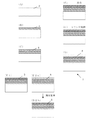
図1に本発明のフォトマスクブランクの一例を示す。図1に示すように本発明のフォトマスクブランク1は、例えば、透明基板2の上に、位相シフト膜3、遮光膜4、珪素含有無機膜5、レジスト膜6が順次形成されているものである。
FIG. 1 shows an example of the photomask blank of the present invention. As shown in FIG. 1, a
フォトマスクブランク1に用いられる透明基板2としては、露光波長で透明な材料で、かつ製造でのそれぞれの工程における処理温度で変形量が小さいものであれば、特に制約はなく、そのようなものの一例としては石英基板が挙げられる。
The
次に、透明基板2の上の膜構成について説明する。
珪素を含有する珪素含有無機膜5としては、後述するようにレジスト膜6と接する面において酸素濃度など所定の条件を満たす必要があるが、膜自体は、例えば、珪素単体、或いは珪素に酸素、窒素、炭素のいずれか1つを少なくとも含むもの、或いは珪素と遷移金属を含むもの、或いは珪素と遷移金属と少なくとも、酸素、窒素、炭素のいずれか1つを含むものであればよい。このようなものとしては珪素からなるもの、酸素と珪素からなるもの、窒素と珪素からなるもの、酸素と窒素と珪素からなるもの、炭素と珪素からなるもの、炭素と酸素と珪素からなるもの、炭素と窒素と珪素からなるもの、炭素と酸素と窒素と珪素からなるもの、遷移金属を含むものとしては遷移金属と珪素からなるもの、遷移金属と珪素と酸素からなるもの、遷移金属と窒素と珪素からなるもの、遷移金属と酸素と窒素と珪素からなるもの、遷移金属と炭素と珪素からなるもの、遷移金属と炭素と酸素と珪素からなるもの、遷移金属と炭素と窒素と珪素からなるもの、遷移金属と炭素と酸素と窒素と珪素からなるものが挙げられるが、特に珪素と酸素と窒素からなるもの(SiON膜)、さらには珪素と酸素からなるもの(SiO膜)が望ましい。
Next, the film configuration on the
The silicon-containing
遷移金属としてはモリブデン、タングステン、タンタル、チタン、ジルコニア、ハフニウムがあげられる。珪素含有無機膜5中の遷移金属としては1種に限らず、2種以上の遷移金属を含んでいてもよい。
さらに水素を含有していてもよい。
Examples of the transition metal include molybdenum, tungsten, tantalum, titanium, zirconia, and hafnium. The transition metal in the silicon-containing
Furthermore, hydrogen may be contained.
また、この珪素含有無機膜5はシリル化処理されたものである。珪素含有無機膜5がシリル化処理されたものであるため、その上に形成されているレジスト膜6との密着性が高い。したがって、レジスト膜6に微細なパターンが形成された場合においても、レジストパターンの倒れや剥がれが生じるのを抑制することができるものである。
The silicon-containing
なお、珪素含有無機膜5に施されるシリル化処理は特に限定されないが、例えば、半導体製造工程で常用されているHMDSを用いた処理とすることができる。
Note that the silylation treatment applied to the silicon-containing
さらに、珪素含有無機膜5は、レジスト膜6と接する面(接触面7)において、酸素濃度が55原子%以上75原子%以下のものである(第一の態様)。
シリル化処理を利用した従来のフォトマスクブランクでは、現像後において、レジスト残渣が多数発生して欠陥が生じてしまっていた。しかしながら、接触面7において上記条件を満たしている本発明のフォトマスクブランク1では、従来品におけるレジスト残渣の発生を抑制でき、欠陥数を低減することができる。
珪素含有無機膜5の接触面7での酸素濃度による欠陥低減の理由は不明だが、例えば、接触面7でのOHの量や、接触面7での原子の結合状態の変化が考えられる。
Furthermore, the silicon-containing
In a conventional photomask blank using a silylation treatment, a large number of resist residues are generated after development, resulting in defects. However, in the
The reason for the reduction of defects due to the oxygen concentration at the contact surface 7 of the silicon-containing
あるいは、珪素含有無機膜5の接触面7において、X線光電子分光法(XPS法)でのSi−Oの結合エネルギーに相当する検出強度がSi−Siの結合エネルギーに相当する検出強度よりも大きいものである(第二の態様)。
Si−OおよびSi−Siの結合エネルギーに相当する検出強度の関係がこのようなものであれば、第一の態様と同様に、現像後のレジスト残渣の抑制および欠陥の低減を図ることができる。
Alternatively, at the contact surface 7 of the silicon-containing
If the relationship between the detected intensities corresponding to the bond energy of Si—O and Si—Si is such, it is possible to suppress resist residues after development and reduce defects as in the first embodiment. .
あるいは、上記の双方の条件を満たすものとすることができる。このようなものであれば、より一層確実に、欠陥数を低減することができる。 Alternatively, both of the above conditions can be satisfied. With such a configuration, the number of defects can be more reliably reduced.
膜構成としてはレジスト膜6の下が珪素含有無機膜5であればよく、例えば、珪素含有無機膜5は、遮光膜、位相シフト膜などの光学膜や、光学膜にパターンを形成するために用いられるハードマスク膜として機能するものであってもよい。また、エッチングストッパを有していてもよい。
特に微細なパターンを形成する時、例えば50nm以下のパターンを形成する時に本発明は有効であり、珪素含有無機膜5をハードマスク膜とするとその効果は大きい。
ハードマスク膜として用いるときの膜厚は好ましくは1−30nm、さらには1−20nm、より好ましくは1−10nmとすると良い。
ここではハードマスク膜としての珪素含有無機膜5と透明基板2の間において、遮光膜4、さらには遮光膜4の下に位相シフト膜3を有する構成となっている。なお、このハードマスク膜としての珪素含有無機膜5と遮光膜4はエッチング選択性がある方が好ましい。
As the film configuration, the silicon-containing
In particular, when forming a fine pattern, for example, when forming a pattern of 50 nm or less, the present invention is effective. When the silicon-containing
The film thickness when used as a hard mask film is preferably 1-30 nm, more preferably 1-20 nm, and even more preferably 1-10 nm.
Here, the structure includes a light shielding film 4 and a phase shift film 3 under the light shielding film 4 between the silicon-containing
ハードマスク(エッチングマスク)膜(珪素含有無機膜5)はCF4やSF6などのフッ素を含むフッ素系エッチングガスでドライエッチングし、遮光膜4などの上記ハードマスク膜の下に形成される無機膜はフッ素系ドライエッチングでは耐性を有し、塩素または塩素と酸素を含むエッチングガスによる塩素系ドライエッチングでエッチングできる材料とすることで、加工が容易にできる。このような遮光膜4などの上記ハードマスク膜の下に形成される無機膜としてはクロムを含有する無機膜が望ましく、例えば、クロム単体や、クロムに酸素、窒素、炭素の少なくとも1種類を有する膜とすることができる。遮光膜4のハードマスク膜側には反射防止層を形成したり、透明基板側にも酸素や窒素の多い膜を形成し、密着性を改善したり、反射防止層としてもよい。 The hard mask (etching mask) film (silicon-containing inorganic film 5) is dry-etched with a fluorine-based etching gas containing fluorine such as CF 4 and SF 6 to form an inorganic film formed under the hard mask film such as the light shielding film 4 The film is resistant to fluorine-based dry etching, and can be easily processed by using a material that can be etched by chlorine-based dry etching using an etching gas containing chlorine or chlorine and oxygen. As the inorganic film formed under the hard mask film such as the light shielding film 4, an inorganic film containing chromium is desirable. For example, chromium alone or at least one of oxygen, nitrogen, and carbon is contained in chromium. It can be a membrane. An antireflection layer may be formed on the hard mask film side of the light shielding film 4, or a film containing a large amount of oxygen or nitrogen may be formed on the transparent substrate side to improve adhesion, or may be used as an antireflection layer.
さらに、遮光膜4と透明基板2の間に位相シフト膜3を形成するときには、該位相シフト膜3は遮光膜4とエッチング特性が異なる方が好ましく、上記のように遮光膜4が塩素と酸素を含むドライエッチングでエッチングされ、フッ素系ドライエッチングに耐性を有する場合は、位相シフト膜3は塩素と酸素を含むエッチングガスによるドライエッチングには耐性を有し、フッ素を含むエッチングでエッチングされる材料とすればよく、例えば珪素に酸素、窒素、炭素のいずれかを少なくとも含む材料とすれば良いし、またはさらに遷移金属を含む材料とすれば良い。遷移金属としてはモリブデン、タングステン、タンタル、チタン、ジルコニア、ハフニウムがあげられる。さらに水素を含有していてもよい。
Further, when the phase shift film 3 is formed between the light shielding film 4 and the
なお、レジスト膜6の下が遮光膜のときは珪素を含む材料としては前述したような材料にすればよく、遮光膜全体を珪素含有無機膜5としてもよい。また、遮光膜の表面を反射防止層とするときは、反射防止層のみを珪素含有無機膜5として、遮光膜を他の材料、例えばクロムを有する膜としてもよい。
When the resist film 6 is under the light shielding film, the material containing silicon may be a material as described above, and the entire light shielding film may be the silicon-containing
また、レジスト膜6の材料としては電子線で描画するための電子線レジストとしてもよいし、光で描画するフォトレジストとしてもよい。特に化学増幅型レジストでその効果は大きい。化学増幅型レジストとしてはポジ型でもネガ型でもよく、ヒドロキシスチレン系の樹脂、酸発生剤を主成分とするもの、さらに架橋剤を添加したもの、クエンチャー、界面活性剤などいずれか1つ以上を含んだものでもよく、また、(メタ)アクリル酸系樹脂としてもよい。 The material of the resist film 6 may be an electron beam resist for drawing with an electron beam or a photoresist drawn with light. The effect is particularly great with a chemically amplified resist. The chemically amplified resist may be positive or negative, and includes at least one of a hydroxystyrene-based resin, an acid generator as a main component, a crosslinking agent added, a quencher, a surfactant, etc. In addition, a (meth) acrylic resin may be used.
次に、図1に示す本発明のフォトマスクブランク1を製造する方法について説明する。図2は本発明の製造方法の一例を示すフロー図である。
まず透明基板2を用意する(図2(A))。透明基板2としては前述したものを用意することができ、例えば石英基板とすることができる。
Next, a method for manufacturing the
First, a
次に、前述したような材料からなる位相シフト膜3(図2(B))および遮光膜4(図2(C))を順次形成する。これらの膜の形成方法は特に限定されず、例えばスパッタリングにより形成することができる。 Next, the phase shift film 3 (FIG. 2B) and the light-shielding film 4 (FIG. 2C) made of the materials described above are sequentially formed. The method for forming these films is not particularly limited, and can be formed, for example, by sputtering.
次に、前述したような材料からなる珪素含有無機膜5を形成する(図2(D1)または図2(D2a)〜図2(D2b))。この珪素含有無機膜5を形成するにあたっては、表面(すなわち、後工程で形成するレジスト膜6と接する面)における酸素濃度が55原子%以上75原子%以下となるようにする。または、表面におけるX線光電子分光法でのSi−Oの結合エネルギーに相当する検出強度がSi−Siの結合エネルギーに相当する検出強度よりも大きくなるようにする。あるいは、上記の双方の条件を満たすようにする。
Next, the silicon-containing
表面の酸素濃度等を上記のように調整してから、後述するシリル化処理を行い、その後にレジスト膜を塗布して形成することによって、レジスト膜6にパターンを描画して現像した際、従来品に比べ、レジスト残渣が生じるのを抑制することができる。そして、これにより欠陥数を大幅に低減することが可能である。 When the surface oxygen concentration and the like are adjusted as described above, a silylation treatment described later is performed, and then a resist film is applied and formed, thereby drawing a pattern on the resist film 6 and developing it. Compared to products, resist residues can be suppressed. As a result, the number of defects can be greatly reduced.
このように表面において酸素濃度等の条件を満たした珪素含有無機膜5を形成するためには、例えばスパッタリングなどにおいて、珪素含有無機膜5を成膜するときの成膜条件を調整することができる(図2(D1))。
または、まず珪素を含有する無機膜を成膜し(予備無機膜8)(図2(D2a))、その後に熱処理やオゾン処理、プラズマ処理などのいずれかを施すことによって表面における酸素濃度等を調整して珪素含有無機膜5を形成することができる(図2(D2b))。
これらの方法であれば、上記のような表面を有する珪素含有無機膜5を簡便に形成できるので好ましい。
Thus, in order to form the silicon-containing
Alternatively, first, an inorganic film containing silicon is formed (preliminary inorganic film 8) (FIG. 2 (D2a)), and then oxygen treatment on the surface is performed by performing any one of heat treatment, ozone treatment, plasma treatment, and the like. The silicon-containing
These methods are preferable because the silicon-containing
なお、この珪素含有無機膜5や予備無機膜8の形成方法としては、珪素を含むガス、例えば、モノシラン、ジクロロシラン、トリクロロシランなどを用いたCVDによる成膜でもよいが、珪素を含有するターゲットを少なくとも1つ用いたスパッタリングによる成膜の方が簡単で制御性よく成膜することができるので好ましい。
The silicon-containing
スパッタリングによる成膜の方法としてはDCスパッタやRFスパッタ法等、特に制約はない。珪素を含む珪素含有無機膜5を成膜するには、例えば珪素と酸素を含む膜とするときはターゲットに珪素を用い、スパッタガスとしてアルゴンと酸素ガスを用いる反応性スパッタリングを行えばよい。また、酸素の代わりに窒素を含む膜を成膜するときは窒素ガスを酸素ガスの代わりに用いればよく、窒素と酸素の両方を含む膜を成膜するときは窒素ガスと酸素ガスを同時に用いてもよいし、また、一酸化窒素や二酸化窒素などの酸化窒素ガスを用いてもよい。炭素をさらに含む膜を成膜するときはメタンガスや一酸化炭素や二酸化炭素などの炭素を含むガスを用いればよい。また、遷移金属をさらに含む膜を成膜するときは遷移金属と珪素を含有したターゲットを用いたり、珪素ターゲットと遷移金属ターゲットの両方を同時に用いて共スパッタリングを行ってもよい。
The film formation method by sputtering is not particularly limited, such as DC sputtering or RF sputtering. In order to form the silicon-containing
さらに、上記成膜により形成した珪素を含む珪素含有無機膜はSi−Siの結合を有する状態の膜であると、この膜を、酸素を含む熱処理を行うことで、表面のSi−Oの結合を熱処理で制御できるため、好ましい。 Further, if the silicon-containing inorganic film containing silicon formed by the above film formation is a film having a Si—Si bond, this film is subjected to a heat treatment containing oxygen to bond Si—O on the surface. Can be controlled by heat treatment.
なお、成膜条件で調整する場合、例えばスパッタリングで成膜するときは成膜するときの雰囲気ガス中のArなどの不活性ガスと酸素や二酸化炭素などの酸化性ガスの比率を調整することによって表面における酸素濃度を調整すればよい。 When adjusting the film formation conditions, for example, when forming a film by sputtering, by adjusting the ratio of an inert gas such as Ar and an oxidizing gas such as oxygen or carbon dioxide in the atmospheric gas during film formation. What is necessary is just to adjust the oxygen concentration in the surface.
また、熱処理で表面における酸素濃度等を調整するとき、熱処理雰囲気中の酸素濃度としては特に制限はなく、例えば、1−100%とすればよい。熱処理の方法としては赤外線加熱、抵抗加熱など特に制約はない。
酸素を含む雰囲気での熱処理温度としては200℃以上とすることが好ましく、400℃以上とすることがより好ましい。
また、オゾン処理やプラズマ処理等においても条件は特に限定されない。表面における酸素濃度等が上記条件を満たすように、これらの処理条件を適宜調整することが可能である。
Further, when adjusting the oxygen concentration or the like on the surface by heat treatment, the oxygen concentration in the heat treatment atmosphere is not particularly limited, and may be, for example, 1 to 100%. There are no particular restrictions on the heat treatment method such as infrared heating or resistance heating.
The heat treatment temperature in an atmosphere containing oxygen is preferably 200 ° C. or higher, and more preferably 400 ° C. or higher.
Also, conditions for ozone treatment, plasma treatment, and the like are not particularly limited. These treatment conditions can be appropriately adjusted so that the oxygen concentration on the surface satisfies the above conditions.
次に洗浄を施してもよい(図2(E))。フォトマスクブランク表面上に存在するパーティクルを除去するためのこの洗浄は、超純水、或いはオゾン、水素などを含んだ超純水である機能水を用い、それと同時に超音波を当てることにより行なうことができる。または界面活性剤入りの超純水で洗浄した後、超純水でリンスし、上記機能水洗浄、UV光照射、または、これらの組み合わせにより行うこともできる。 Next, you may wash | clean (FIG.2 (E)). This cleaning to remove particles present on the photomask blank surface should be performed by using ultrapure water or functional water that is ultrapure water containing ozone, hydrogen, etc. and simultaneously applying ultrasonic waves. Can do. Alternatively, after washing with ultrapure water containing a surfactant, rinsing with ultrapure water may be performed by the functional water washing, UV light irradiation, or a combination thereof.
そして、フォトマスクブランク表面の表面エネルギーを低減させておくためのシリル化処理を行い、フォトマスクブランク表面をアルキルシリル化する(図2(F))。このようなシリル化処理を行うことによって、微細レジストパターンの剥がれや倒れを防止することができる。 Then, silylation treatment for reducing the surface energy of the photomask blank surface is performed to alkylsilylate the photomask blank surface (FIG. 2F). By performing such a silylation treatment, peeling or falling of the fine resist pattern can be prevented.
シリル化剤としては、前述したようにHMDSが挙げられるが、これに限定されない。
シリル化処理の方法としては基板の珪素含有無機膜の上に直接塗布する方法や、上記シリル化剤に基板を暴露する方法がある。暴露方法としては、基板を保持した容器中で上記シリル化剤を蒸発させる方法、あるいは、窒素ガスをバブリングすることによって上記シリル化剤を気化させる方法などがある。上記シリル化剤を反応させる温度としては、例えば40℃以上200℃以下とすることができる。また処理時間としては、例えば、予め、シリル化処理の同条件で水の接触角を測定し、基板の濡れ性が適当な値となるように調整することが好ましい。
Examples of the silylating agent include HMDS as described above, but are not limited thereto.
As a silylation treatment method, there are a method of directly coating on the silicon-containing inorganic film of the substrate and a method of exposing the substrate to the silylating agent. Examples of the exposure method include a method of evaporating the silylating agent in a container holding a substrate, or a method of vaporizing the silylating agent by bubbling nitrogen gas. As temperature which makes the said silylating agent react, it can be 40 degreeC or more and 200 degrees C or less, for example. The treatment time is preferably adjusted, for example, by previously measuring the contact angle of water under the same conditions for the silylation treatment so that the wettability of the substrate becomes an appropriate value.
そして、シリル化処理した珪素含有無機膜5上に、前述したようなレジスト膜6を塗布し、本発明のフォトマスクブランク1を得ることができる(図2(G))。
なお塗布方法は特に限定されず、例えば従来と同様の方法で行うことができる。パターン形状が良好に得られるよう、適宜膜厚等決定することができる。
And the resist film 6 as mentioned above is apply | coated on the silicon-containing
In addition, the coating method is not specifically limited, For example, it can carry out by the method similar to the past. The film thickness and the like can be appropriately determined so that the pattern shape can be obtained satisfactorily.
以下、実施例及び比較例を示して本発明をより具体的に説明するが、本発明はこれらに限定されるものではない。
(実施例1)
本発明の製造方法により、本発明のフォトマスクブランクを製造した。
152mm角、厚み約6mmの石英基板上に位相シフト膜としてMoSiONをスパッタ法で75nm形成した。スパッタガスとしては酸素と窒素とアルゴンを用い、ターゲットとしてはMoSi2とSiの2種類を用いて、基板を30rpmで回転させながら成膜した。
この位相シフト膜の組成をESCA(Electron Spectroscopy for Chemical Analysis)法(XPS法)(サーモフィッシャーサイエンティフィック株式会社製 K−Alpha)で調べたところMo:Si:O:N=1:4:1:4(原子比)であった。
EXAMPLES Hereinafter, although an Example and a comparative example are shown and this invention is demonstrated more concretely, this invention is not limited to these.
Example 1
The photomask blank of the present invention was manufactured by the manufacturing method of the present invention.
75 nm of MoSiON was formed as a phase shift film on a 152 mm square quartz substrate having a thickness of about 6 mm by sputtering. Oxygen, nitrogen, and argon were used as the sputtering gas, and MoSi 2 and Si were used as the targets, and the film was formed while rotating the substrate at 30 rpm.
The composition of the phase shift film was examined by ESCA (Electron Spectroscopic for Chemical Analysis) (XPS method) (K-Alpha manufactured by Thermo Fisher Scientific Co., Ltd.), and Mo: Si: O: N = 1: 4: 1. : 4 (atomic ratio).
この上に、さらに遮光膜として基板側からCrNからなる層(30nm)とCrONからなる層(20nm)をスパッタ法で形成した。スパッタガスとしては、CrN層はアルゴンと窒素ガスを、CrON層は酸素と窒素とアルゴンを用い、ターゲットとしては金属クロムを用いて、基板を30rpmで回転させながら成膜した。
この遮光膜の組成をESCAで調べたところCrN層はCr:N=9:1(原子比)、CrON層はCr:O:N=4:5:1(原子比)であった。
On this, a layer made of CrN (30 nm) and a layer made of CrON (20 nm) were further formed by sputtering as a light shielding film from the substrate side. As the sputtering gas, argon and nitrogen gas were used for the CrN layer, oxygen, nitrogen and argon were used for the CrON layer, and metal chromium was used as the target, and the film was formed while rotating the substrate at 30 rpm.
When the composition of this light shielding film was examined by ESCA, the CrN layer was Cr: N = 9: 1 (atomic ratio), and the CrON layer was Cr: O: N = 4: 5: 1 (atomic ratio).
この上に、珪素を含むエッチングマスク膜(ハードマスク)として5nmの厚さのSiOをスパッタ法で形成した。スパッタガスとしては酸素とアルゴンを用い、ターゲットとしてはSiを用いて、基板を30rpmで回転させながら成膜した。
さらにこれに熱処理を行った。熱処理雰囲気としては酸素を含む雰囲気とし、熱処理温度は500℃とした。
このエッチングマスク膜の組成をESCAで調べたところ表面の酸素濃度は61.5原子%であった。
On top of this, 5 nm thick SiO was formed by sputtering as an etching mask film (hard mask) containing silicon. Oxygen and argon were used as the sputtering gas, Si was used as the target, and the film was formed while rotating the substrate at 30 rpm.
This was further heat-treated. The heat treatment atmosphere was an atmosphere containing oxygen, and the heat treatment temperature was 500 ° C.
When the composition of this etching mask film was examined by ESCA, the oxygen concentration on the surface was 61.5 atomic%.
また、エッチングマスク膜の表面をESCA法で調べ、Si−Oの結合エネルギーに相当する検出強度とSi−Siの結合エネルギーに相当する検出強度を図3に示す。
その結果、Si−Oの結合エネルギーに相当する検出強度(面積強度)がSi−Siの結合エネルギーに相当する検出強度よりも大きいことが観察された(図3参照)。
Further, the surface of the etching mask film is examined by the ESCA method, and the detected intensity corresponding to the Si—O bond energy and the detected intensity corresponding to the Si—Si bond energy are shown in FIG.
As a result, it was observed that the detected intensity (area intensity) corresponding to the Si—O bond energy was larger than the detected intensity corresponding to the Si—Si bond energy (see FIG. 3).
これをHMDSを用いたシリル化処理を行った後、ネガ型電子線レジスト(信越化学工業株式会社製)を塗布したのち、水酸化テトラメチルアンモニウムで現像してレジストパターンを得て、その後、純水でリンスした。 After performing silylation treatment using HMDS, this was coated with a negative electron beam resist (manufactured by Shin-Etsu Chemical Co., Ltd.) and developed with tetramethylammonium hydroxide to obtain a resist pattern. Rinse with water.
これを欠陥検査装置MAGICS 2350(レーザーテック社製)で検査した結果、図4のような欠陥数が極めて少ない良好な結果となった。
なお、検出された0.1μm以上の欠陥の数は42個であった。
As a result of inspecting this with a defect inspection apparatus MAGICS 2350 (manufactured by Lasertec Corporation), the number of defects as shown in FIG.
The number of detected defects of 0.1 μm or more was 42.
(実施例2)
熱処理温度を300℃に変えた以外は実施例1と同様にして、本発明のフォトマスクブランク(熱処理後のエッチングマスク膜の表面の酸素濃度は55.6原子%、Si−O結合の検出強度>Si−Si結合の検出強度)を得た(図3参照)。
その結果、現像後の欠陥の数は1180個であった。
(Example 2)
The photomask blank of the present invention (the oxygen concentration on the surface of the etching mask film after the heat treatment was 55.6 atomic%, the detected intensity of the Si—O bond was the same as in Example 1 except that the heat treatment temperature was changed to 300 ° C. > Detected intensity of Si—Si bond) (see FIG. 3).
As a result, the number of defects after development was 1180.
(実施例3)
SiOをスパッタ法で形成する際のスパッタガス中の酸素量を調整したこと、およびスパッタ後の熱処理を行わなかったこと以外は実施例1と同様にして、本発明のフォトマスクブランク(エッチングマスク膜の表面の酸素濃度は71.0原子%、Si−O結合の検出強度>Si−Si結合の検出強度)を得た。
その結果、現像後の欠陥の数は30個であった。
(Example 3)
The photomask blank (etching mask film) of the present invention is the same as in Example 1 except that the amount of oxygen in the sputtering gas when SiO is formed by the sputtering method is adjusted, and the heat treatment after sputtering is not performed. The surface oxygen concentration was 71.0 atomic%, Si—O bond detection intensity> Si—Si bond detection intensity).
As a result, the number of defects after development was 30.
(比較例)
熱処理を行わなかったこと以外は実施例1と同様にしてフォトマスクブランク(エッチングマスク膜の表面の酸素濃度は52.6原子%、Si−O結合の検出強度<Si−Si結合の検出強度)を作製した。
現像後に欠陥検査した結果、図5のような多数のレジスト残渣が残った。検出された0.1μm以上の欠陥の数は4704個と非常に多かった。
なお、このときのSiOの結合エネルギーに相当する強度がSi−Siの結合の強度よりも小さかった(図3参照)。
(Comparative example)
Photomask blank (the etching mask film surface oxygen concentration is 52.6 atomic%, Si—O bond detection intensity <Si—Si bond detection intensity) in the same manner as in Example 1 except that no heat treatment was performed. Was made.
As a result of defect inspection after development, a large number of resist residues as shown in FIG. 5 remained. The number of detected defects of 0.1 μm or more was very large at 4704.
In addition, the intensity | strength corresponded to the bond energy of SiO at this time was smaller than the intensity | strength of the bond of Si-Si (refer FIG. 3).
特に、実施例2と比較例を比較して分かるように、実施例2のようにエッチングマスク膜の表面の酸素濃度を55原子%以上(あるいは、Si−O結合の検出強度>Si−Si結合の検出強度)とすることによって、55原子%未満(あるいは、Si−O結合の検出強度<Si−Si結合の検出強度)の比較例よりも欠陥数を1/4以下に著しく低減できていることが分かる。
また、実施例1(酸素濃度:61.5原子%、欠陥数:42個)や実施例3(酸素濃度:71.0原子%、欠陥数:30個)から分かるように、欠陥数を抑制するにあたっては、上記酸素濃度を75%程度にまで調整すれば十分であると言える。
In particular, as can be seen by comparing Example 2 with a comparative example, the oxygen concentration on the surface of the etching mask film is 55 atomic% or more as in Example 2 (or Si—O bond detection intensity> Si—Si bond). ), The number of defects can be remarkably reduced to ¼ or less than the comparative example of less than 55 atomic% (or Si—O bond detection intensity <Si—Si bond detection intensity). I understand that.
Further, as can be seen from Example 1 (oxygen concentration: 61.5 atomic%, number of defects: 42) and Example 3 (oxygen concentration: 71.0 atomic%, number of defects: 30), the number of defects is suppressed. In doing so, it can be said that it is sufficient to adjust the oxygen concentration to about 75%.
なお、本発明は、上記実施形態に限定されるものではない。上記実施形態は、例示であり、本発明の特許請求の範囲に記載された技術的思想と実質的に同一な構成を有し、同様な作用効果を奏するものは、いかなるものであっても本発明の技術的範囲に包含される。 The present invention is not limited to the above embodiment. The above-described embodiment is an exemplification, and the present invention has substantially the same configuration as the technical idea described in the claims of the present invention, and any device that exhibits the same function and effect is the present invention. It is included in the technical scope of the invention.
1…本発明のフォトマスクブランク、 2…透明基板、 3…位相シフト膜、
4…遮光膜、 5…珪素含有無機膜、 6…レジスト膜、
7…接触面、 8…予備無機膜。
DESCRIPTION OF
4 ... light-shielding film, 5 ... silicon-containing inorganic film, 6 ... resist film,
7: Contact surface, 8 ... Preliminary inorganic film.
Claims (17)
前記レジスト膜と接することになる表面におけるX線光電子分光法でのSi−Oの結合エネルギーに相当する検出強度がSi−Siの結合エネルギーに相当する検出強度よりも大きい前記珪素含有無機膜を形成した後、シリル化処理を行い、その後、塗布により前記レジスト膜を形成することを特徴とするフォトマスクブランクの製造方法。 A method for producing a photomask blank having a silicon-containing inorganic film containing at least silicon on a transparent substrate, and having a resist film on the silicon-containing inorganic film,
Forming the silicon-containing inorganic film having a detected intensity corresponding to the Si—O bond energy in the X-ray photoelectron spectroscopy on the surface that will be in contact with the resist film greater than the detected intensity corresponding to the Si—Si bond energy. Then, a silylation treatment is performed, and then the resist film is formed by coating.
前記レジスト膜と接することになる表面における酸素濃度が55原子%以上75原子%以下の前記珪素含有無機膜を、前記透明基板上に珪素を含有する無機膜を成膜してからオゾン処理、プラズマ処理のうちのいずれかの処理を行うことによって形成した後、シリル化処理を行い、その後、塗布により前記レジスト膜を形成することを特徴とするフォトマスクブランクの製造方法。 A method for producing a photomask blank having a silicon-containing inorganic film containing at least silicon on a transparent substrate, and having a resist film on the silicon-containing inorganic film,
The silicon-containing inorganic film having an oxygen concentration of 55 atomic% or more and 75 atomic% or less on the surface in contact with the resist film is formed on the transparent substrate, and then an ozone treatment, plasma A method for producing a photomask blank, comprising: forming by performing any one of the processes, performing a silylation process, and then forming the resist film by coating.
前記珪素含有無機膜は、前記透明基板上に珪素を含有する無機膜を成膜してからオゾン処理、プラズマ処理のうちのいずれかの処理を行うことによって形成されたものであり、前記レジスト膜と接する面における酸素濃度が55原子%以上75原子%以下のものであることを特徴とするフォトマスクブランク。 A photomask blank having, on a transparent substrate, at least a silicon-containing inorganic film subjected to silylation treatment containing silicon, and having a resist film on the silicon-containing inorganic film,
The silicon-containing inorganic film is formed by forming an inorganic film containing silicon on the transparent substrate and then performing any one of ozone treatment and plasma treatment, and the resist film A photomask blank having an oxygen concentration of 55 atomic% or more and 75 atomic% or less on a surface in contact with the surface.
前記珪素含有無機膜は、前記レジスト膜と接する面におけるX線光電子分光法でのSi−Oの結合エネルギーに相当する検出強度がSi−Siの結合エネルギーに相当する検出強度よりも大きいものであることを特徴とするフォトマスクブランク。 A photomask blank having, on a transparent substrate, at least a silicon-containing inorganic film subjected to silylation treatment containing silicon, and having a resist film on the silicon-containing inorganic film,
In the silicon-containing inorganic film, the detection intensity corresponding to the Si—O binding energy in X-ray photoelectron spectroscopy on the surface in contact with the resist film is larger than the detection intensity corresponding to the Si—Si binding energy. A photomask blank characterized by that.
Priority Applications (9)
| Application Number | Priority Date | Filing Date | Title |
|---|---|---|---|
| JP2014164960A JP6258151B2 (en) | 2013-09-25 | 2014-08-13 | Photomask blank and manufacturing method thereof |
| US14/489,019 US9488906B2 (en) | 2013-09-25 | 2014-09-17 | Photomask blank and method for manufacturing photomask blank |
| EP14003227.7A EP2863258B1 (en) | 2013-09-25 | 2014-09-17 | Photomask blank and method for manufacturing photomask blank |
| TW103133005A TWI615671B (en) | 2013-09-25 | 2014-09-24 | Photomask blank and method for manufacturing photomask blank |
| KR1020140127571A KR101917407B1 (en) | 2013-09-25 | 2014-09-24 | Photomask blank and method for manufacturing photomask blank |
| CN201810596424.7A CN108594593A (en) | 2013-09-25 | 2014-09-25 | Photomask blank and its manufacturing method |
| CN201910904266.1A CN110609437A (en) | 2013-09-25 | 2014-09-25 | Photomask blank and method for manufacturing same |
| CN201410499354.5A CN104460221A (en) | 2013-09-25 | 2014-09-25 | Photomask blank and method for manufacturing photomask blank |
| US15/284,098 US9709885B2 (en) | 2013-09-25 | 2016-10-03 | Photomask blank and method for manufacturing photomask blank |
Applications Claiming Priority (5)
| Application Number | Priority Date | Filing Date | Title |
|---|---|---|---|
| JP2013198585 | 2013-09-25 | ||
| JP2013198585 | 2013-09-25 | ||
| JP2014159610 | 2014-08-05 | ||
| JP2014159610 | 2014-08-05 | ||
| JP2014164960A JP6258151B2 (en) | 2013-09-25 | 2014-08-13 | Photomask blank and manufacturing method thereof |
Publications (2)
| Publication Number | Publication Date |
|---|---|
| JP2016035546A JP2016035546A (en) | 2016-03-17 |
| JP6258151B2 true JP6258151B2 (en) | 2018-01-10 |
Family
ID=51570251
Family Applications (1)
| Application Number | Title | Priority Date | Filing Date |
|---|---|---|---|
| JP2014164960A Active JP6258151B2 (en) | 2013-09-25 | 2014-08-13 | Photomask blank and manufacturing method thereof |
Country Status (6)
| Country | Link |
|---|---|
| US (2) | US9488906B2 (en) |
| EP (1) | EP2863258B1 (en) |
| JP (1) | JP6258151B2 (en) |
| KR (1) | KR101917407B1 (en) |
| CN (3) | CN104460221A (en) |
| TW (1) | TWI615671B (en) |
Families Citing this family (12)
| Publication number | Priority date | Publication date | Assignee | Title |
|---|---|---|---|---|
| JP6601245B2 (en) * | 2015-03-04 | 2019-11-06 | 信越化学工業株式会社 | Photomask blank, photomask manufacturing method, and mask pattern forming method |
| WO2016140044A1 (en) * | 2015-03-04 | 2016-09-09 | 信越化学工業株式会社 | Photomask blank, method for manufacturing photomask, and mask pattern formation method |
| JP6523873B2 (en) * | 2015-08-27 | 2019-06-05 | Hoya株式会社 | Method of manufacturing mask blank, method of manufacturing transfer mask, and mask blank |
| JP6713336B2 (en) * | 2016-04-21 | 2020-06-24 | Hoya株式会社 | Mask blank manufacturing method and transfer mask manufacturing method |
| CN106933023A (en) * | 2017-05-09 | 2017-07-07 | 深圳市华星光电技术有限公司 | A kind of preparation method of light shield and substrate of glass |
| JP6791031B2 (en) * | 2017-06-13 | 2020-11-25 | 信越化学工業株式会社 | Photomask blank and its manufacturing method |
| JP6753375B2 (en) * | 2017-07-28 | 2020-09-09 | 信越化学工業株式会社 | Photomask blank, photomask blank manufacturing method and photomask manufacturing method |
| JP6819546B2 (en) * | 2017-11-13 | 2021-01-27 | 信越化学工業株式会社 | Photomask blank and photomask manufacturing method |
| WO2020138855A1 (en) * | 2018-12-26 | 2020-07-02 | 주식회사 에스앤에스텍 | Blank mask and photomask |
| JP7313166B2 (en) * | 2019-03-18 | 2023-07-24 | Hoya株式会社 | Mask blank, method for manufacturing transfer mask, and method for manufacturing semiconductor device |
| JP7303077B2 (en) * | 2019-09-10 | 2023-07-04 | アルバック成膜株式会社 | Method for manufacturing mask blanks, method for manufacturing photomask, mask blanks and photomask |
| TWI791990B (en) * | 2020-05-15 | 2023-02-11 | 力晶積成電子製造股份有限公司 | Method of forming photomask and method of manufacturing ion implantation mask |
Family Cites Families (28)
| Publication number | Priority date | Publication date | Assignee | Title |
|---|---|---|---|---|
| JPS6385553A (en) | 1986-09-30 | 1988-04-16 | Toshiba Corp | Mask substrate and mask pattern forming method |
| JPH0749558A (en) | 1993-08-05 | 1995-02-21 | Sony Corp | Production of phase shift mask |
| JP3294976B2 (en) * | 1995-09-29 | 2002-06-24 | ホーヤ株式会社 | Phase shift mask and phase shift mask blank |
| JP4054951B2 (en) | 2001-08-06 | 2008-03-05 | 信越化学工業株式会社 | Method for manufacturing phase shift mask blank and method for manufacturing phase shift mask |
| SE0201019D0 (en) | 2002-04-04 | 2002-04-04 | Micronic Laser Systems Ab | A mask blank and a method for producing the same |
| US20040159538A1 (en) * | 2003-02-13 | 2004-08-19 | Hans Becker | Photo mask blank, photo mask, method and apparatus for manufacturing of a photo mask blank |
| JP2005055597A (en) * | 2003-08-01 | 2005-03-03 | Toppan Printing Co Ltd | Method for manufacturing halftone phase shift mask and pattern transfer method |
| CN100565307C (en) * | 2004-02-13 | 2009-12-02 | 株式会社半导体能源研究所 | Semiconductor devices and preparation method thereof, liquid crystal television system and EL television system |
| US20050196710A1 (en) * | 2004-03-04 | 2005-09-08 | Semiconductor Energy Laboratory Co., Ltd. | Method for forming pattern, thin film transistor, display device and method for manufacturing the same, and television apparatus |
| JP2006078825A (en) * | 2004-09-10 | 2006-03-23 | Shin Etsu Chem Co Ltd | Photomask blank, photomask and method for manufacturing same |
| TWI375114B (en) * | 2004-10-22 | 2012-10-21 | Shinetsu Chemical Co | Photomask-blank, photomask and fabrication method thereof |
| WO2006049595A1 (en) * | 2004-10-27 | 2006-05-11 | International Business Machines Corporation | Recovery of hydrophobicity of low-k and ultra low-k organosilicate films used as inter metal dielectrics |
| CN100465353C (en) * | 2004-12-24 | 2009-03-04 | 中国科学院兰州化学物理研究所 | Method for preparing composite film of carbon similar to generic diamond containing Nano granules of silicon dioxide |
| JP4766507B2 (en) * | 2005-03-30 | 2011-09-07 | Hoya株式会社 | Phase shift mask blank and method of manufacturing phase shift mask |
| JP4509050B2 (en) | 2006-03-10 | 2010-07-21 | 信越化学工業株式会社 | Photomask blank and photomask |
| JP4807739B2 (en) * | 2006-03-30 | 2011-11-02 | Hoya株式会社 | Mask blank and photomask |
| JP4737426B2 (en) * | 2006-04-21 | 2011-08-03 | 信越化学工業株式会社 | Photomask blank |
| JP4936515B2 (en) * | 2006-05-18 | 2012-05-23 | Hoya株式会社 | Photomask manufacturing method and halftone phase shift mask manufacturing method |
| JP2009122566A (en) * | 2007-11-19 | 2009-06-04 | Dainippon Printing Co Ltd | Low reflection type photomask blank and photomask |
| KR20100102159A (en) * | 2007-12-27 | 2010-09-20 | 알박 세이마쿠 가부시키가이샤 | Mask blank, production method of mask blank and production method of mask |
| TWI452419B (en) * | 2008-01-28 | 2014-09-11 | Az Electronic Mat Ip Japan Kk | Fine pattern mask, process for producing the same, and process for forming fine pattern by using the same |
| JP4833356B2 (en) | 2009-02-13 | 2011-12-07 | Hoya株式会社 | PHOTO MASK BLANK AND ITS MANUFACTURING METHOD, PHOTO MASK AND SEMICONDUCTOR DEVICE MANUFACTURING METHOD |
| CN101660128A (en) * | 2009-09-27 | 2010-03-03 | 南京大学 | Gate dielectric material cubical phase HfO2 film and preparation method thereof |
| JP5704754B2 (en) * | 2010-01-16 | 2015-04-22 | Hoya株式会社 | Mask blank and transfer mask manufacturing method |
| EP2650729A4 (en) * | 2010-12-09 | 2014-07-16 | Nissan Chemical Ind Ltd | Composition for forming resist underlayer film containing hydroxyl group-containing carbazole novolac resin |
| TWI588599B (en) * | 2011-04-06 | 2017-06-21 | Hoya股份有限公司 | Surface treatment method for a mask blank, method of manufacturing a mask blank, and method of manufacturing a mask |
| KR102211544B1 (en) | 2013-01-15 | 2021-02-02 | 호야 가부시키가이샤 | Mask blank, phase-shift mask, and method for manufacturing semiconductor device |
| JP6005530B2 (en) * | 2013-01-15 | 2016-10-12 | Hoya株式会社 | Mask blank, phase shift mask and manufacturing method thereof |
-
2014
- 2014-08-13 JP JP2014164960A patent/JP6258151B2/en active Active
- 2014-09-17 US US14/489,019 patent/US9488906B2/en active Active
- 2014-09-17 EP EP14003227.7A patent/EP2863258B1/en active Active
- 2014-09-24 KR KR1020140127571A patent/KR101917407B1/en active IP Right Grant
- 2014-09-24 TW TW103133005A patent/TWI615671B/en active
- 2014-09-25 CN CN201410499354.5A patent/CN104460221A/en active Pending
- 2014-09-25 CN CN201910904266.1A patent/CN110609437A/en active Pending
- 2014-09-25 CN CN201810596424.7A patent/CN108594593A/en active Pending
-
2016
- 2016-10-03 US US15/284,098 patent/US9709885B2/en active Active
Also Published As
| Publication number | Publication date |
|---|---|
| US9488906B2 (en) | 2016-11-08 |
| KR20150034113A (en) | 2015-04-02 |
| TWI615671B (en) | 2018-02-21 |
| TW201527868A (en) | 2015-07-16 |
| JP2016035546A (en) | 2016-03-17 |
| CN104460221A (en) | 2015-03-25 |
| EP2863258A3 (en) | 2015-06-03 |
| CN108594593A (en) | 2018-09-28 |
| US9709885B2 (en) | 2017-07-18 |
| US20150086908A1 (en) | 2015-03-26 |
| CN110609437A (en) | 2019-12-24 |
| US20170023855A1 (en) | 2017-01-26 |
| EP2863258B1 (en) | 2021-06-23 |
| KR101917407B1 (en) | 2018-11-09 |
| EP2863258A2 (en) | 2015-04-22 |
Similar Documents
| Publication | Publication Date | Title |
|---|---|---|
| JP6258151B2 (en) | Photomask blank and manufacturing method thereof | |
| JP6234898B2 (en) | Photomask blank manufacturing method | |
| JP6601245B2 (en) | Photomask blank, photomask manufacturing method, and mask pattern forming method | |
| TW201944167A (en) | Semiconductor device fabrication method | |
| JP6740107B2 (en) | Mask blank, transfer mask, and semiconductor device manufacturing method | |
| TW201131286A (en) | Photomask blank and method of manufacturing photomask | |
| CN111902772A (en) | Mask blank, phase shift mask and method for manufacturing semiconductor device | |
| JP2017044892A (en) | Method for manufacturing mask blank, method for manufacturing transfer mask, and mask blank | |
| JP5939662B2 (en) | Mask blank manufacturing method | |
| WO2016140044A1 (en) | Photomask blank, method for manufacturing photomask, and mask pattern formation method | |
| TWI824153B (en) | Blank photomask, photomask manufacturing method and photomask | |
| JP2017194588A (en) | Surface treatment method, method for manufacturing mask blank and method for manufacturing transfer mask | |
| JP7331793B2 (en) | Photomask manufacturing method and photomask blank | |
| JP2011221250A (en) | Photomask and method for manufacturing photomask |
Legal Events
| Date | Code | Title | Description |
|---|---|---|---|
| A621 | Written request for application examination |
Free format text: JAPANESE INTERMEDIATE CODE: A621 Effective date: 20160728 |
|
| A977 | Report on retrieval |
Free format text: JAPANESE INTERMEDIATE CODE: A971007 Effective date: 20170413 |
|
| A131 | Notification of reasons for refusal |
Free format text: JAPANESE INTERMEDIATE CODE: A131 Effective date: 20170425 |
|
| A521 | Written amendment |
Free format text: JAPANESE INTERMEDIATE CODE: A523 Effective date: 20170619 |
|
| TRDD | Decision of grant or rejection written | ||
| A01 | Written decision to grant a patent or to grant a registration (utility model) |
Free format text: JAPANESE INTERMEDIATE CODE: A01 Effective date: 20171121 |
|
| A61 | First payment of annual fees (during grant procedure) |
Free format text: JAPANESE INTERMEDIATE CODE: A61 Effective date: 20171206 |
|
| R150 | Certificate of patent or registration of utility model |
Ref document number: 6258151 Country of ref document: JP Free format text: JAPANESE INTERMEDIATE CODE: R150 |