JP6255179B2 - Display device - Google Patents
Display device Download PDFInfo
- Publication number
- JP6255179B2 JP6255179B2 JP2013144385A JP2013144385A JP6255179B2 JP 6255179 B2 JP6255179 B2 JP 6255179B2 JP 2013144385 A JP2013144385 A JP 2013144385A JP 2013144385 A JP2013144385 A JP 2013144385A JP 6255179 B2 JP6255179 B2 JP 6255179B2
- Authority
- JP
- Japan
- Prior art keywords
- electrode
- electrodes
- display device
- period
- touch
- Prior art date
- Legal status (The legal status is an assumption and is not a legal conclusion. Google has not performed a legal analysis and makes no representation as to the accuracy of the status listed.)
- Active
Links
- 238000001514 detection method Methods 0.000 claims description 48
- 239000000758 substrate Substances 0.000 claims description 29
- 239000004973 liquid crystal related substance Substances 0.000 claims description 25
- 238000012937 correction Methods 0.000 claims description 23
- 230000008859 change Effects 0.000 claims description 10
- 230000005484 gravity Effects 0.000 claims description 5
- 230000002093 peripheral effect Effects 0.000 claims description 3
- 238000006243 chemical reaction Methods 0.000 description 39
- 230000035945 sensitivity Effects 0.000 description 20
- 238000010586 diagram Methods 0.000 description 19
- 230000000052 comparative effect Effects 0.000 description 18
- 230000005540 biological transmission Effects 0.000 description 11
- 230000008878 coupling Effects 0.000 description 8
- 238000010168 coupling process Methods 0.000 description 8
- 238000005859 coupling reaction Methods 0.000 description 8
- 230000009467 reduction Effects 0.000 description 8
- 230000010354 integration Effects 0.000 description 7
- 239000000203 mixture Substances 0.000 description 5
- 230000007423 decrease Effects 0.000 description 4
- 230000006870 function Effects 0.000 description 4
- 239000003990 capacitor Substances 0.000 description 3
- 239000004020 conductor Substances 0.000 description 2
- 239000010410 layer Substances 0.000 description 2
- 238000000034 method Methods 0.000 description 2
- 230000004044 response Effects 0.000 description 2
- 239000003566 sealing material Substances 0.000 description 2
- 238000013459 approach Methods 0.000 description 1
- 230000005684 electric field Effects 0.000 description 1
- 239000011521 glass Substances 0.000 description 1
- 230000006872 improvement Effects 0.000 description 1
- 239000011159 matrix material Substances 0.000 description 1
- 238000005259 measurement Methods 0.000 description 1
- 238000012986 modification Methods 0.000 description 1
- 230000004048 modification Effects 0.000 description 1
- 239000011241 protective layer Substances 0.000 description 1
Images


Classifications
-
- G—PHYSICS
- G06—COMPUTING; CALCULATING OR COUNTING
- G06F—ELECTRIC DIGITAL DATA PROCESSING
- G06F3/00—Input arrangements for transferring data to be processed into a form capable of being handled by the computer; Output arrangements for transferring data from processing unit to output unit, e.g. interface arrangements
- G06F3/01—Input arrangements or combined input and output arrangements for interaction between user and computer
- G06F3/03—Arrangements for converting the position or the displacement of a member into a coded form
- G06F3/041—Digitisers, e.g. for touch screens or touch pads, characterised by the transducing means
- G06F3/044—Digitisers, e.g. for touch screens or touch pads, characterised by the transducing means by capacitive means
- G06F3/0443—Digitisers, e.g. for touch screens or touch pads, characterised by the transducing means by capacitive means using a single layer of sensing electrodes
-
- G—PHYSICS
- G06—COMPUTING; CALCULATING OR COUNTING
- G06F—ELECTRIC DIGITAL DATA PROCESSING
- G06F3/00—Input arrangements for transferring data to be processed into a form capable of being handled by the computer; Output arrangements for transferring data from processing unit to output unit, e.g. interface arrangements
- G06F3/01—Input arrangements or combined input and output arrangements for interaction between user and computer
- G06F3/03—Arrangements for converting the position or the displacement of a member into a coded form
- G06F3/041—Digitisers, e.g. for touch screens or touch pads, characterised by the transducing means
- G06F3/0412—Digitisers structurally integrated in a display
-
- G—PHYSICS
- G06—COMPUTING; CALCULATING OR COUNTING
- G06F—ELECTRIC DIGITAL DATA PROCESSING
- G06F3/00—Input arrangements for transferring data to be processed into a form capable of being handled by the computer; Output arrangements for transferring data from processing unit to output unit, e.g. interface arrangements
- G06F3/01—Input arrangements or combined input and output arrangements for interaction between user and computer
- G06F3/03—Arrangements for converting the position or the displacement of a member into a coded form
- G06F3/041—Digitisers, e.g. for touch screens or touch pads, characterised by the transducing means
- G06F3/0416—Control or interface arrangements specially adapted for digitisers
- G06F3/0418—Control or interface arrangements specially adapted for digitisers for error correction or compensation, e.g. based on parallax, calibration or alignment
-
- G—PHYSICS
- G06—COMPUTING; CALCULATING OR COUNTING
- G06F—ELECTRIC DIGITAL DATA PROCESSING
- G06F3/00—Input arrangements for transferring data to be processed into a form capable of being handled by the computer; Output arrangements for transferring data from processing unit to output unit, e.g. interface arrangements
- G06F3/01—Input arrangements or combined input and output arrangements for interaction between user and computer
- G06F3/03—Arrangements for converting the position or the displacement of a member into a coded form
- G06F3/041—Digitisers, e.g. for touch screens or touch pads, characterised by the transducing means
- G06F3/044—Digitisers, e.g. for touch screens or touch pads, characterised by the transducing means by capacitive means
- G06F3/0445—Digitisers, e.g. for touch screens or touch pads, characterised by the transducing means by capacitive means using two or more layers of sensing electrodes, e.g. using two layers of electrodes separated by a dielectric layer
-
- G—PHYSICS
- G06—COMPUTING; CALCULATING OR COUNTING
- G06F—ELECTRIC DIGITAL DATA PROCESSING
- G06F3/00—Input arrangements for transferring data to be processed into a form capable of being handled by the computer; Output arrangements for transferring data from processing unit to output unit, e.g. interface arrangements
- G06F3/01—Input arrangements or combined input and output arrangements for interaction between user and computer
- G06F3/03—Arrangements for converting the position or the displacement of a member into a coded form
- G06F3/041—Digitisers, e.g. for touch screens or touch pads, characterised by the transducing means
- G06F3/044—Digitisers, e.g. for touch screens or touch pads, characterised by the transducing means by capacitive means
- G06F3/0446—Digitisers, e.g. for touch screens or touch pads, characterised by the transducing means by capacitive means using a grid-like structure of electrodes in at least two directions, e.g. using row and column electrodes
Landscapes
- Engineering & Computer Science (AREA)
- General Engineering & Computer Science (AREA)
- Theoretical Computer Science (AREA)
- Human Computer Interaction (AREA)
- Physics & Mathematics (AREA)
- General Physics & Mathematics (AREA)
- Position Input By Displaying (AREA)
Description
本開示は、表示装置に関し、例えばタッチパネルを有する表示装置に適用可能である。 The present disclosure relates to a display device and can be applied to a display device having a touch panel, for example.
液晶表示装置は液晶表示パネルを有し、液晶表示パネルは2枚の基板の間に液晶組成物を封止した構成となっている。また、液晶表示パネルの前面に入力装置としてタッチパネルを配置したものが量産されている。このタッチパネルの入力(以下タッチと称する)の検出に静電容量や抵抗値の変化を用いるものが提案されている。 The liquid crystal display device has a liquid crystal display panel, and the liquid crystal display panel has a configuration in which a liquid crystal composition is sealed between two substrates. In addition, a liquid crystal display panel in which a touch panel is arranged as an input device on the front surface is mass-produced. A device that uses a change in capacitance or resistance to detect an input (hereinafter referred to as touch) of the touch panel has been proposed.
静電容量の変化を検出するタッチパネルとは、絶縁膜を介して配置された2枚の電極間の静電容量の変化を検出するもので、以下、静電容量方式のタッチパネルという。静電容量方式のタッチパネルには、表示パネルの外に設けられる外付型(特許文献1)と表示パネルの中に設けられる内蔵型がある。内蔵型には、表示パネルにもともと備えられている表示用の共通電極(対向電極)を、一対のタッチセンサ用電極のうちの一方として兼用し、他方の電極(タッチ検出電極)をこの共通電極と交差するように配置した、いわゆるインセルタイプの表示パネルがある(特許文献2)。 A touch panel that detects a change in capacitance detects a change in capacitance between two electrodes arranged via an insulating film, and is hereinafter referred to as a capacitive touch panel. The capacitive touch panel includes an external type (Patent Document 1) provided outside the display panel and a built-in type provided in the display panel. In the built-in type, the display common electrode (counter electrode) originally provided in the display panel is also used as one of the pair of touch sensor electrodes, and the other electrode (touch detection electrode) is used as the common electrode. There is a so-called in-cell type display panel that is arranged so as to intersect with (Patent Document 2).
本願発明者らは静電容量結合方式タッチパネルを検討した結果、以下の問題があることを見出した。
すなわち、静電容量結合方式タッチパネルでは、パネル表示部の中心部に比べてパネル表示部の端近傍において、タッチ位置の検出座標精度が劣る。
As a result of examining the capacitive coupling type touch panel, the present inventors have found that there are the following problems.
That is, in the capacitively coupled touch panel, the detection coordinate accuracy of the touch position is inferior in the vicinity of the end of the panel display unit as compared with the center of the panel display unit.
本開示のうち、代表的なものの概要を簡単に説明すれば、下記のとおりである。
すなわち、表示装置は、タッチパネル検出電極において、パネル表示部の端の電極の周期を小さくする。
The outline of a representative one of the present disclosure will be briefly described as follows.
That is, the display device reduces the period of the electrode at the end of the panel display unit in the touch panel detection electrode.
上記表示装置によれば、パネル表示部の端近傍での検出座標精度が改善される。 According to the display device, the detection coordinate accuracy near the edge of the panel display unit is improved.
以下、図面を参照して実施例を説明する。なお、実施例を説明するための全図において、同一機能を有するものは同一符号を付け、その繰り返しの説明は省略する。 Embodiments will be described below with reference to the drawings. In all the drawings for explaining the embodiments, parts having the same functions are given the same reference numerals, and repeated explanation thereof is omitted.
以下の実施例においては、液晶表示装置を例にとって説明するが、有機EL表示装置などの他の形式の表示装置についても適用することができる。 In the following embodiments, a liquid crystal display device will be described as an example, but the present invention can also be applied to other types of display devices such as an organic EL display device.
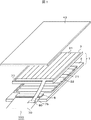
図1は実施例1に係る液晶表示装置の基本構成を示す概略図である。同図に示すように、液晶表示装置100は、液晶表示パネル1と、駆動回路5と、フレキシブル基板70と、フロントパネル40と、収納ケース(図示せず)、バックライト(図示せず)とから構成される。
FIG. 1 is a schematic diagram illustrating a basic configuration of the liquid crystal display device according to the first embodiment. As shown in the figure, the liquid
液晶表示パネル1は、TFT基板2とカラーフィルタ基板3とを所定の間隙を隔てて重ね合わせ、該両基板間の周縁部近傍に枠状に設けたシール材(図示せず)により、両基板を貼り合わせると共に、シール材の内側に液晶組成物を封入、封止し、さらに、両基板の外側に偏光板を貼り付けて構成される。
The liquid
TFT基板2には、対向電極21と、駆動回路5から対向電極21に接続された対向電極信号線22が設けられている。駆動回路5から対向電極信号が対向電極信号線22を介して対向電極21に伝えられる。カラーフィルタ基板3には検出電極31が設けられ、検出電極31は接続部77でフレキシブル基板75と接続している。フレキシブル基板75はフレキシブル基板70とコネクタ80で接続している。検出電極31から検出信号がフレキシブル基板75、コネクタ80、フレキシブル基板70を介して駆動回路5に伝えられる。
The
なお、液晶表示パネル1は多数の画素をマトリクス状に備えた表示部(詳細については後述する)を有している。対向電極21は共通電極であり、画素において画素電極と対向してTFT基板2に配置されている。すなわち、液晶表示パネル1はFFS(Fringe Field Switching)やIPS(In Plane Switching)等の横電界方式である。両電極間に電圧を印加することで液晶分子の配向が変化する。この液晶分子の配向の変化に伴い、パネルを透過する光の割合が変化することで画像が表示される。
The liquid
次に図2を用いて対向電極21と検出電極31について説明する。前述したように、対向電極21はTFT基板2上に設けられている共通電極であるが、タッチ検出用駆動電極として使用するために図2のように分割されている。駆動回路5から対向電極21に対向電極信号が供給される。この対向電極信号は、主に共通電極の電圧が印加されていて、画素に書き込みしていないタイミングでタッチの検出に用いられる駆動信号が印加される。
Next, the
駆動信号が対向電極21に印加されると、対向電極21と一定の間隔を持って配置され容量を構成する検出電極31に検出信号が生じる。この検出信号は検出電極用端子36を介して外部に取り出される。
When a drive signal is applied to the
なお、検出電極31の両側にはダミー電極33が形成されている。ダミー電極33はいずれの電極や配線にも接続されていない。検出電極31は一方の端部でダミー電極33側に向かい広がりT字状の検出電極用端子36を形成している。また、TFT基板2には対向電極信号線22以外にも駆動回路用入力端子25のような様々な配線、端子等が形成される。
Note that
図3に表示部の断面の一部を拡大した概略断面図を示す。図3に示すようにTFT基板2には画素部200が設けられており対向電極21は画素の一部として画像表示に用いられる。また、TFT基板2とカラーフィルタ基板3との間には液晶組成物(液晶層)4が狭持されている。カラーフィルタ基板3に設けられた検出電極31とTFT基板2に設けられた対向電極21とは容量を形成しており、対向電極21に駆動信号が印加されると検出電極31の電圧が変化する。この時図3に示すようにフロントパネル40を介して指108等の導電体が近接または接触すると、容量に変化が生じ検出電極31に生じる電圧に、近接・接触が無い場合に比較して変化が生じる。
FIG. 3 shows a schematic cross-sectional view in which a part of the cross section of the display unit is enlarged. As shown in FIG. 3, the
このように、液晶表示パネル1に形成した対向電極21と検出電極31との間に生じる容量の変化を検出することで、液晶表示パネル1にタッチパネルの機能を備えることが可能となる。
Thus, by detecting a change in capacitance generated between the
図4Aから図4Dは静電容量型インセルタッチパネルの電極の平面パターンを模式的に示す図である。説明の都合上、対向電極(送信側電極、Tx電極)21が7本、検出電極(受信側電極、Rx電極)31が5本の場合を示している。図4Aは通常の電極パターン(比較例1)、図4Bは端電極の周期を変更した第1の例(電極パターンを調整)、図4Cは端電極の周期を変更した第2の例(電極パターンを単純カット)、図4Dは端電極の周期を変更した第3の例(電極パターンを比例縮小)である。 4A to 4D are diagrams schematically showing a planar pattern of electrodes of a capacitive in-cell touch panel. For convenience of explanation, a case where there are seven counter electrodes (transmission side electrodes, Tx electrodes) 21 and five detection electrodes (reception side electrodes, Rx electrodes) 31 is shown. 4A is a normal electrode pattern (Comparative Example 1), FIG. 4B is a first example in which the period of the end electrode is changed (adjusted electrode pattern), and FIG. 4C is a second example in which the period of the end electrode is changed (electrode) FIG. 4D shows a third example (the electrode pattern is proportionally reduced) in which the cycle of the end electrodes is changed.
図4Aの比較例1では、Tx電極21の幅および間隔がすべて同じで、Rx電極31の幅および間隔がすべて同じである。Tx電極21の幅はTx電極21の間隔よりも大きく、Rx電極31の幅はRx電極31の間隔よりも小さい。Tx電極21の周期(PTx)は横破線の間隔で、すべて一定である。Rx電極31の周期(PRx)は縦破線の間隔で、すべて一定である。Tx電極21は横破線間の中心に、Rx電極31は縦破線間の中心に位置している。
In Comparative Example 1 of FIG. 4A, the width and interval of the
図4Bの端電極の周期を変更した第1の例では、端のTx電極(Tx1、Tx7)211、217の幅が他のTx電極21の幅より小さく、端のTx電極(Tx1、Tx7)211、217の周期(PTxe)が他のTx電極21の周期(PTx)より小さくなっている(PTxe<PTx)。また、端のRx電極(Rx1、Rx5)311、315の周期(PRxe)が他のRx電極31の周期(PRx)より小さくなっている(PRxe<PRx)。端のRx電極(Rx1、Rx5)311、315とTx電極のX方向の端までの距離が短くなっている。すなわち、端のRx電極(Rx1、Rx5)311、315は縦破線間の中心からTx電極のX方向の端の方にずれている。このとき、端のRx電極(例えばRx1)とその隣のRx電極(例えばRx2)の間の距離を変えないことが、内側のRx電極(Rx2)の感度を変えないための工夫である。また、周期の縮小に合わせて端のRx電極311、315の幅を縮小している。周期の縮小により端電極での感度は低下するが、端のRx電極311、315の幅を同時に縮小することで、感度の低下を緩和している。
In the first example in which the cycle of the end electrodes in FIG. 4B is changed, the widths of the end Tx electrodes (Tx1, Tx7) 21 1 , 21 7 are smaller than the widths of the
図4Cの端電極の周期を変更した第2の例は、端のTx電極と端のRx電極パターンを単純カットしたものである。図4Cにおいても端のRx電極311C、315Cの周期(PRxe)を他のRx電極31の周期(PRx)よりも縮小しているが、端のRx電極311C、315Cの幅を変えていない点で図4Bと異なっている。この場合、図4Bよりも感度が低下するが、座標精度改善には効果がある。なお、Tx電極は図4Bと同じである。
In the second example in which the cycle of the end electrode in FIG. 4C is changed, the end Tx electrode and the end Rx electrode pattern are simply cut. Although reduced than the period of the Rx electrodes 31 1C, 31 5C period (P Rxe)
図4Dの端電極の周期を変更した第3の例は、端のTx電極と端のRx電極パターンを比例縮小したものである。図4Dにおいても端のRx電極の周期(PRxe)を他のRx電極の周期(PRx)よりも縮小しているが、端のRx電極311D、315Dの領域で比例縮小しているため、端のRx電極311D、315Dと隣のRx電極31の間の距離が変わってしまう点で図4Bと異なっている。この場合、1つ内側の電極の感度が多少低下するが、座標精度改善には効果がある。端のRx電極311D、315Dの領域で比例縮小しているので、端のRx電極311D、315Dの幅が他のRx電極31の幅よりも小さくなっており、また端のRx電極(Rx1、Rx5)311D、315Dは縦破線間の中心に位置している。なお、Tx電極は図4Bと同じである。
The third example in which the period of the end electrode in FIG. 4D is changed is a proportional reduction of the end Tx electrode and the end Rx electrode pattern. While shrinking than even the period of Rx electrode end period of the (P Rxe) other Rx electrode (P Rx) in FIG. 4D, is proportional reduction in the area of the Rx electrodes 31 1D, 31 5D end Therefore , it is different from FIG. 4B in that the distance between the
<座標精度改善の原理>
端の電極周期縮小により座標精度が改善する理由は、パネル端近傍へのタッチに対して端の電極1本のみで反応する領域が小さくなり、複数本の電極が反応するためである。これについて説明する。
<Principle of coordinate accuracy improvement>
The reason that the coordinate accuracy is improved by reducing the electrode cycle at the end is that the region that reacts with only one end electrode with respect to the touch near the end of the panel is reduced, and a plurality of electrodes react. This will be described.
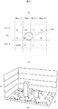
座標計算として、各Tx電極とRx電極の交点(Tx−Rxの交点)のタッチに対する反応値の重心をタッチ検出座標とする方法がよく用いられる。本開示でもこの方法を想定する。簡単のため、Tx電極周期(PTx)とRx電極周期(PRx)を等しいとして、タッチする疑似指の直径(=2rとする)も電極周期に等しいとして説明する。パネル端近傍でのタッチが中央と異なるのは、片方の隣に電極が無いことである。 As the coordinate calculation, a method is often used in which the centroid of the reaction value for the touch at the intersection of each Tx electrode and Rx electrode (intersection of Tx-Rx) is the touch detection coordinate. This method is also assumed in the present disclosure. For simplicity, it is assumed that the Tx electrode period (P Tx ) is equal to the Rx electrode period (P Rx ), and the diameter of the pseudo finger to be touched (= 2r) is also equal to the electrode period. The touch near the edge of the panel is different from the center in that there is no electrode next to one.
図5はパネルの中央をタッチしたときの反応を示す図である。図5(a)はパネルのタッチ位置を、図5(b)は反応値を示している。図5(a)に示すように疑似指FFの中心は交点6に位置するが疑似指FFは交点7にも及んでいる。図5(b)に示すようにパネル中央のタッチでは交点6と交点7に大きな反応があり、重心計算によりタッチ位置の中心が精度良く求められる。図6は比較例1に係るパネルの端をタッチしたときの反応を示す図である。図6(a)はパネルのタッチ位置を、図6(b)は反応値を示している。図6(a)に示すように疑似指FFの中心は交点4に位置するが疑似指FFは端よりも外に及んでいる。図6(b)に示すようにパネルの端近傍でのタッチでは、大きな反応が交点4しかなく、横方向の検出精度が良くない。なお、破線と破線の間に電極がある
これを図7Aから図7Cでもう少し詳しく見る。図7Aは比較例1に係るパネルの端(x=0)をタッチしたときの反応を示す図である。図7A(a)はパネルのタッチ位置を、図7A(b)は反応値を示している。図7A(a)に示すように疑似指FFの中心はパネルの端(x=0)に位置する。図7A(b)に示すように、x=0の位置では、電極RxNの交点しか反応していない。図7Bは比較例1に係るパネルの端からr/2の位置(x=r/2)をタッチしたときの反応を示す図である。図7B(a)はパネルのタッチ位置を、図7B(b)は反応値を示している。図7B(a)に示すように、疑似指FFの中心はパネルの端(x=r/2)に位置する。図7B(b)に示すように、x=r/2の位置で交点3に少し反応が現れるが、まだノイズと大差ないレベルのため、座標計算に寄与しない。その結果、パネル端ではx=0からx=r/2の位置までRxNの1本のみで反応しているため、x方向の位置の違いが検出できない。即ち、タッチ位置がx=0からx=r/2までの間、検出座標の位置が変わらない。これがパネル端で座標精度が劣化する原因である。図7Cは比較例1に係るパネルの端からrの位置(x=r)をタッチしたときの反応を示す図である。図7C(a)はパネルのタッチ位置を、図7C(b)は反応値を示している。図7C(a)に示すように、疑似指FFの中心はパネルの端(x=r)に位置する。図7C(b)に示すように、x=rでは交点3の反応値が十分大きくなり、座標計算に寄与している。
FIG. 5 is a diagram showing a reaction when the center of the panel is touched. FIG. 5A shows the touch position of the panel, and FIG. 5B shows the reaction value. As shown in FIG. 5A, the center of the pseudo finger FF is located at the
端の電極周期を縮小した場合を図8Aから図8Cに示す。図8Aは実施例1に係るパネルの端(x=0)をタッチしたときの反応を示す図である。図8A(a)はパネルのタッチ位置を、図8A(b)は反応値を示している。図8A(a)に示すように疑似指FFの中心はパネルの端(x=0)に位置する。図8A(b)に示すように、x=0での交点4の反応値は図7A(b)(比較例1)よりも小さいが、図8A(b)では交点3に既に多少の反応がある。図8Bは実施例1に係るパネルの端からr/2の位置(x=r/2)をタッチしたときの反応を示す図である。図8B(a)はパネルのタッチ位置を、図8B(b)は反応値を示している。図8B(a)に示すように、疑似指FFの中心はパネルの端(x=r/2)に位置する。図8B(b)に示すように、x=r/2では既に十分に大きな反応値となっていて、重心計算に寄与する。図8Cは実施例1に係るパネルの端からrの位置(x=r)をタッチしたときの反応を示す図である。図8C(a)はパネルのタッチ位置を、図8C(b)は反応値を示している。図8C(a)に示すように、疑似指FFの中心はパネルの端(x=r)に位置する。図8C(b)に示すように、x=rでは交点3の反応値が十分大きくなり、座標計算に寄与している。つまり、端の電極周期を縮小した場合は、x=0付近でもタッチ位置が変わったことを検知できる。以上の理由により、パネル端での座標精度が改善する。
8A to 8C show a case where the end electrode period is reduced. FIG. 8A is a diagram illustrating a reaction when the end (x = 0) of the panel according to the first embodiment is touched. FIG. 8A (a) shows the touch position of the panel, and FIG. 8A (b) shows the reaction value. As shown in FIG. 8A (a), the center of the pseudo finger FF is located at the end (x = 0) of the panel. As shown in FIG. 8A (b), the reaction value at the
なお、端のRx電極の例で説明してきたが、Tx電極の端でも同様である。検出座標精度が改善されることで、タッチパネルで線や絵を描く場合に、パネル表示部の端近傍でもタッチで描いた軌跡と同じ軌跡が、歪み無しに出力される。 The example of the end Rx electrode has been described, but the same applies to the end of the Tx electrode. By improving the detection coordinate accuracy, when a line or a picture is drawn on the touch panel, the same locus as the locus drawn by the touch is output without distortion even near the edge of the panel display unit.
<感度の補正>
周期変更により端電極の感度が変わるため、座標計算時にソフトウェアで感度を補正する。Tx−Rx交点の感度は、概算では、その交点の領域面積(Tx周期×Rx周期)に比例する。そのため、端のTx電極と端のRx電極の周期を縮小した場合に、最も感度が低下するのは4隅(コーナー)の交点である。ソフトウェアで感度を補正してもノイズは補正できないので、この4隅の交点でS/N比を確保することが必要であり、この条件により周期縮小の限界が決まる。
<Sensitivity correction>
Since the sensitivity of the end electrode changes by changing the period, the sensitivity is corrected by software when calculating the coordinates. The sensitivity of the Tx-Rx intersection is roughly proportional to the area of the intersection (Tx period × Rx period). Therefore, when the period of the end Tx electrode and the end Rx electrode is reduced, the sensitivity is most lowered at the intersection of the four corners. Since noise cannot be corrected even if the sensitivity is corrected by software, it is necessary to secure an S / N ratio at the intersections of these four corners, and this condition determines the limit of period reduction.
図9は感度補正のフローチャートである。A/DコンバータからTx−Rx各交点のSijを得る(ステップS91)。Tx−Rx交点の位置によって感度補正値が異なるので、Tx−Rx交点の位置を判定する(ステップS92)。交点(i,j)でのタッチ反応値をSij、感度補正されたタッチ反応値をS’ij、X方向端での感度補正値をAx、Y方向端での感度補正値をAy、コーナーでの感度補正値をAcとする。なお、タッチがなければSij=0であるが、ノイズがあるため常に0にはならない。X方向の端では、S’ij=Sij×Ax、とする(ステップS93)。ここで、Ax≒中央のX方向の周期/端のX方向の周期、である。Y方向の端では、S’ij=Sij×Ay、とする(ステップS94)。ここで、Ay≒中央のY方向の周期/端のY方向の周期、である。コーナーでは、S’ij=Sij×Ac、とする(ステップS95)。ここで、Ac≒Ax×Ay、である。中央(端以外)では、S’ij=Sij(補正なし)、とする(ステップS96)。各交点のS’ijに基づいて、重心計算してタッチ検出座標を求める(ステップS97)。重心計算して求めたタッチ検出座標について端補補正を行う(ステップS98)。端補正については後述する端補正を行った座標をホスト(Host)側へ出力する(ステップS99)。 FIG. 9 is a flowchart of sensitivity correction. Sij of each intersection of Tx-Rx is obtained from the A / D converter (step S91). Since the sensitivity correction value differs depending on the position of the Tx-Rx intersection, the position of the Tx-Rx intersection is determined (step S92). The touch response value at the intersection (i, j) is Sij, the sensitivity corrected touch response value is S'ij, the sensitivity correction value at the X direction end is Ax, the sensitivity correction value at the Y direction end is Ay, and the corner is Let the sensitivity correction value of Ac be Ac. If there is no touch, Sij = 0, but it is not always 0 due to noise. At the end in the X direction, S′ij = Sij × Ax (step S93). Here, Ax≈the cycle in the center X direction / the cycle in the X direction at the end. At the end in the Y direction, S′ij = Sij × Ay (step S94). Here, Ay≈the center Y-direction period / the end Y-direction period. At the corner, S′ij = Sij × Ac (step S95). Here, Ac≈Ax × Ay. At the center (other than the end), S′ij = Sij (no correction) is set (step S96). Based on S′ij of each intersection, the center of gravity is calculated to obtain touch detection coordinates (step S97). Edge correction is performed on the touch detection coordinates obtained by calculating the center of gravity (step S98). For end correction, coordinates after end correction described later are output to the host (Host) side (step S99).
<端補正>
図10Aは比較例1に係る外周座標補正を説明する図である。X方向の電極周期をPxとすると、通常パターン(比較例1)においては、重心計算での各交点の周期もPxとなる。X方向の全体の電極幅をLとすると、単純重心計算でのタッチ座標の取り得る範囲はPx/2〜L−Px/2となる。そこで、Px/2〜Pxの座標を0〜Pxに、L−Px〜L−Px/2の座標をL−Px〜Lに変換する補正を行う。この補正を端補正または外周座標補正という。
<Edge correction>
FIG. 10A is a diagram for explaining outer periphery coordinate correction according to the first comparative example. Assuming that the electrode period in the X direction is Px, in the normal pattern (Comparative Example 1), the period of each intersection in the centroid calculation is also Px. Assuming that the entire electrode width in the X direction is L, the possible range of touch coordinates in simple centroid calculation is Px / 2 to L-Px / 2. Therefore, correction is performed to convert the coordinates of Px / 2 to Px to 0 to Px and the coordinates of L-Px to L-Px / 2 to L-Px to L. This correction is called end correction or outer peripheral coordinate correction.
図10Bは実施例1に係る外周座標補正を説明する図である。端の電極周期を縮小したパターン(実施例1)においては、重心計算での各交点の周期がPxとなるように、端の交点の位置を定義する。X方向の端の電極周期をPex、X方向の全体の電極幅をL’とすると、単純重心計算でのタッチ座標の取り得る範囲はPex−Px/2〜L’−Pex+Px/2となる。そこで、Pex−Px/2〜2(Pex−Px/2)の座標を0〜2(Pex−Px/2)に、L’−2(Pex+Px/2)〜L’−Pex+Px/2の座標をL’−2(Pex+Px/2)〜L’に変換する補正を行う。 FIG. 10B is a diagram illustrating the outer periphery coordinate correction according to the first embodiment. In the pattern in which the electrode cycle at the end is reduced (Example 1), the position of the end intersection is defined so that the cycle of each intersection in the centroid calculation is Px. Assuming that the electrode period at the end in the X direction is Pex and the entire electrode width in the X direction is L ′, the possible range of touch coordinates in simple centroid calculation is Pex−Px / 2 to L′−Pex + Px / 2. Therefore, the coordinates of Pex-Px / 2 to 2 (Pex-Px / 2) are set to 0 to 2 (Pex-Px / 2), and the coordinates of L'-2 (Pex + Px / 2) to L'-Pex + Px / 2 are set. Correction for conversion from L′−2 (Pex + Px / 2) to L ′ is performed.
以上の説明はX方向の端補正であるが、Y方向も同様に補正を行う。 Although the above description is the end correction in the X direction, the Y direction is similarly corrected.
<交点毎のキャリブレーション>
周期縮小により端でのキャリブレーション値が変わるため、各Tx−Rx交点毎にキャリブレーションを行う。
先ず、キャリブレーションについて説明する。タッチ検出回路の基本構成(キャブレーション回路なし)例を図11に示す。また、タッチ検出の波形の例を図12に示す。図12(a)はTxパルスの電圧波形を、図12(b)は結合電流の電流波形を、図12(c)は積分出力の電圧波形を、図12(d)は図12(c)を拡大した積分出力の電圧波形を示す。タッチ検出回路51は、積分回路52とアナログ/デジタル変換回路(A/D変換回路、A/D Converter)53を有する。積分回路52は、演算増幅器54と積分容量Cintと参照電圧源Vrefを有する。Tx電極にTxパルスが印加されるとRx電極にTx−Rxの結合容量Cxyに基づくパルス状の結合電流が流れる。この結合電流を積分回路52で電圧に変換する。積分回路52の出力(積分出力)をA/D変換回路53でデジタル値に変換する。タッチによりTx−Rxの結合容量Cxyが変化することでタッチを検出する。
<Calibration at each intersection>
Since the calibration value at the end changes due to the period reduction, calibration is performed at each Tx-Rx intersection.
First, calibration will be described. An example of the basic configuration of the touch detection circuit (without a calibration circuit) is shown in FIG. An example of a touch detection waveform is shown in FIG. 12A shows the voltage waveform of the Tx pulse, FIG. 12B shows the current waveform of the coupling current, FIG. 12C shows the voltage waveform of the integrated output, and FIG. 12D shows the voltage waveform of FIG. The voltage waveform of the integrated output is shown by enlarging. The
しかし、タッチ時と非タッチ時との結合容量Cxyの変化量(ΔCxy)は、図12(d)に示すように、結合容量Cxyの10%〜20%程度であるため、積分出力にオフセット(Offset)をかけて、A/D変換の範囲を適切に設定する。このOffsetをかけることを、タッチパネルのキャリブレーションと呼び、Offset量を決める設定値をキャリブレーション値としている。図12(d)のAの部分をA/D変換の範囲とするように、Bの部分をキャリブレーションによりOffsetする。 However, since the change amount (ΔCxy) of the coupling capacitance Cxy between the touch time and the non-touch time is about 10% to 20% of the coupling capacitance Cxy as shown in FIG. Offset) and set the A / D conversion range appropriately. Applying this offset is called touch panel calibration, and a setting value for determining the offset amount is used as a calibration value. The portion B is offset by calibration so that the portion A in FIG. 12D is within the A / D conversion range.
図13はキャリブレーション機能を有するタッチ検出回路の基本構成を示す図である。タッチ検出回路51cは、積分回路52とA/D変換回路53と電流源55を有する。積分回路52は、演算増幅器54と積分容量Cintと参照電圧源Vrefを有する。Offset量は、図13の回路では、キャリブレーション電流の積分値である。なお、図11〜13はTxパルス1回分の波形を示しているが、通常1フレーム、1Tx電極当たり複数回のパルスを積算してタッチ検出を行う。
FIG. 13 is a diagram showing a basic configuration of a touch detection circuit having a calibration function. The touch detection circuit 51 c includes an
端の電極周期を縮小すると、概ね交点の領域面積(Tx周期×Rx周期)に比例してCxyも減少する。つまり、必要なOffset量が端の電極と中央の電極で異なる。そのため、各交点毎にキャリブレーションを行い、各交点毎にキャリブレーション値を記録する。キャリブレーションは、表示装置の出荷時に行い、キャリブレーション値をEEPROMやフラッシュメモリ等の不揮発性メモリに記憶しておき、表示装置の起動ごとにキャリブレーション値を読み込むようにされる。 When the electrode cycle at the end is reduced, Cxy also decreases in proportion to the area of the intersection (Tx cycle × Rx cycle). That is, the required offset amount differs between the end electrode and the center electrode. Therefore, calibration is performed for each intersection and a calibration value is recorded for each intersection. The calibration is performed when the display device is shipped, and the calibration value is stored in a nonvolatile memory such as an EEPROM or a flash memory, and the calibration value is read every time the display device is activated.
図14は実施例1に係るキャリブレーションのフローチャートである。キャリブレーション値を中央の値に設定する(ステップS141)。非タッチ状態で検出動作を行う(ステップS142)。積分出力電圧をVout、キャリブレーションにより非タッチでのVoutが目標とする電圧をVz、収束判定定数をεとし、Voutの値を判定する(ステップS143)。Vout>Vz+εの場合は、キャリブレーション電流を減らす方向にキャリブレーション値を変更する(ステップS144)。Vout<Vz−εの場合は、キャリブレーション電流を増やす方向にキャリブレーション値を変更する(ステップS145)。|Vout−Vz|<εの場合は、キャリブレーション値を決定する(ステップS146)。 FIG. 14 is a flowchart of calibration according to the first embodiment. The calibration value is set to the center value (step S141). The detection operation is performed in a non-touch state (step S142). The integrated output voltage is set to Vout, the voltage targeted for non-touch Vout by calibration is set to Vz, the convergence determination constant is set to ε, and the value of Vout is determined (step S143). If Vout> Vz + ε, the calibration value is changed in a direction to reduce the calibration current (step S144). If Vout <Vz−ε, the calibration value is changed in the direction of increasing the calibration current (step S145). If | Vout−Vz | <ε, a calibration value is determined (step S146).
Tx電極はどれか1つのTx電極を選んでパルスを出すが、Rx電極は同時に動作するので、1つのTx電極に対してすべてのRx電極が同時にキャリブレーションを行う。これを全てのTx電極について行う。 The Tx electrode selects any one Tx electrode and outputs a pulse. However, since the Rx electrodes operate simultaneously, all the Rx electrodes simultaneously perform calibration for one Tx electrode. This is performed for all Tx electrodes.
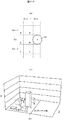
図15は、実施例2のタッチパネル装置の全体構成を示すブロック図である。本実施例のタッチパネル装置300は、静電容量方式のタッチパネル301と、容量検出部302と、制御部303と、バス接続信号線35とから構成される。タッチパネル301には、ユーザのタッチを検出するためのセンサ端子である電極パターン(X電極341およびY電極342)が形成されている。X電極341およびY電極342は、容量検出部302に接続される。容量検出部302は、X電極341を送信電極(駆動電極)として順次パルス印加を行い、Y電極342を受信電極とすることで、各電極交点における電極間容量(相互容量)を測定する。制御部303は、前述の各電極交点における電極間容量の測定結果に基づいてタッチ検出を行い、バス接続信号線335を介して、検出結果をホストへ通知する。
FIG. 15 is a block diagram illustrating the overall configuration of the touch panel device according to the second embodiment. The
図16は、実施例2のタッチパネルの断面構造を示す概略断面図である。タッチパネル301は、基板層323を底面とし、Y電極341とX電極342、保護層322を積層させ、表面ガラス321を貼り付けた構造をもっている。なお、言うまでもないが、本実施例のタッチパネル301は、表示パネル(例えば、液晶表示パネル、有機EL表示パネルなど)上に搭載される。図16の構成において、指360でタッチパネル301をタッチした時の電気力線の状態を示す図である。指(擬似接地された導体)360がシールドとなり、電気力線324を妨げている。これにより、X電極341とY電極342の間の電極間容量値(相互容量値)は減少する。
FIG. 16 is a schematic cross-sectional view illustrating a cross-sectional structure of the touch panel according to the second embodiment. The
図17Aから図17Cは静電容量型外付け型タッチパネルの電極の平面パターンを模式的に示す図である。説明の都合上、Y電極(送信側電極、Tx電極)342が7本、X電極(受信側電極、Rx電極)341が5本の場合を示している。図17Aは通常の電極パターン(比較例2)、図17Bは端電極の周期を変更した第1の例(電極パターンを調整)、図17Cは端電極の周期を変更した第2の例(電極パターンを比例縮小)である。 FIG. 17A to FIG. 17C are diagrams schematically showing a planar pattern of electrodes of a capacitive external touch panel. For convenience of explanation, the case where there are seven Y electrodes (transmission side electrodes, Tx electrodes) 342 and five X electrodes (reception side electrodes, Rx electrodes) 341 is shown. FIG. 17A is a normal electrode pattern (Comparative Example 2), FIG. 17B is a first example in which the period of the end electrode is changed (adjusted electrode pattern), and FIG. 17C is a second example in which the period of the end electrode is changed (electrode) The pattern is proportionally reduced).
図17Aの比較例2では、Tx電極342の幅および間隔がすべて同じで、Rx電極341の幅および間隔がすべて同じである。Tx電極342の周期(PTx)は横破線の間隔で、すべて一定である。Rx電極341の周期(PRx)は縦破線の間隔で、すべて一定である。Tx電極342は横破線間の中心に、Rx電極341は縦破線間の中心に位置している。
In Comparative Example 2 of FIG. 17A, the width and interval of the
図17Bの端電極の周期を変更した第1の例では、端のTx電極(Tx1とTx7)3421、3427の幅が他のTx電極342の幅より小さく、端のTx電極3421、3427の周期(PTxe)が他のTx電極342の周期(PTx)より小さくなっている(PTxe<PTx)。また、端のRx電極(Rx1とRx5)3411、3415の幅が他のRx電極341の幅より小さく、端のRx電極3411、3415の周期(PRxe)が他のRx電極341の周期(PRx)より小さくなっている(PRxe<PRx)。端のTx電極(Tx1、Tx7)3421、3427がRx電極と交差する部分は横破線間の中心からRx電極のY方向の端の方にずれている。端のRx電極(Rx1、Rx5)3411、3415がTx電極と交差する部分は縦破線間の中心からTx電極のX方向の端の方にずれている。このとき、端のRx電極(例えばRx1)とその隣のRx電極(例えばRx2)に接する部分の、Tx電極のひし形を変形しないことが、1つ内側のRx電極(Rx2)の感度を変えないための工夫である。
In the first example in which the period of the end electrode in FIG. 17B is changed, the widths of the end Tx electrodes (Tx1 and Tx7) 342 1 and 342 7 are smaller than the widths of the
図17Cの端電極の周期を変更した第2の例は、端のTx電極と端のRx電極パターンを比例縮小したものである。図17Cにおいても、端のTx電極3421C、3427Cの周期(PTxe)及び端のRx電極3411C、3415Cの周期(PRxe)が小さくなっているが、端のRx電極3411C、3415Cの領域で比例縮小したため、端のRx電極3411C、3415CがTx電極と交差する部分と隣のRx電極341とTx電極が交差する部分の間の距離が変わってしまう点で図17Bと異なっている。端のTx電極3421C、3427Cの領域で比例縮小しているので、端のTx電極3421C、3427Cの幅が他のTx電極342の幅よりも小さくなっており、また端のTx電極(Tx1、Tx7)3421C、3427Cは横破線間の中心に位置している。端のRx電極3411C、3415Cの領域で比例縮小しているので、端のRx電極3411C、3415Cの幅が他のRx電極341の幅よりも小さくなっており、また端のRx電極(Rx1、Rx5)3411C、3415Cは縦破線間の中心に位置している。この場合、1つ内側の電極の感度が多少低下するが、座標精度改善には効果がある。
A second example in which the period of the end electrode in FIG. 17C is changed is a proportional reduction of the end Tx electrode and the end Rx electrode pattern. Also in FIG. 17C, the period of the
上記のように端の電極周期を縮小した場合は、実施例1と同じ理由により、パネル端での座標精度が改善する。検出座標精度が改善されることで、タッチパネルで線や絵を描く場合に、パネル表示部の端近傍でもタッチで描いた軌跡と同じ軌跡が、歪み無しに出力される。 When the edge electrode period is reduced as described above, the coordinate accuracy at the panel edge is improved for the same reason as in the first embodiment. By improving the detection coordinate accuracy, when a line or a picture is drawn on the touch panel, the same locus as the locus drawn by the touch is output without distortion even near the edge of the panel display unit.
以上、本発明者によってなされた発明を実施例に基づき具体的に説明したが、本発明は、上記実施例に限定されるものではなく、種々変更可能であることはいうまでもない。 As mentioned above, the invention made by the present inventor has been specifically described based on the embodiments. However, the present invention is not limited to the above-described embodiments, and needless to say, various modifications can be made.
21・・・対向電極(送信側電極、Tx電極)
211、217・・・端のTx電極
31・・・検出電極(受信側電極、Rx電極)
311、315・・・端のRx電極
PRx・・・Rx電極の周期
PRxe・・・端のRx電極の周期
PTx・・・Tx電極の周期
PTxe・・・端のTx電極の周期
21 ... Counter electrode (transmission side electrode, Tx electrode)
21 1 , 21 7 ...
31 1 , 31 5 ... End Rx electrode P Rx ... Rx electrode period P Rxe ... End Rx electrode period P Tx ... Tx electrode period P Txe ... End Tx electrode Cycle
Claims (14)
所定周期で第1方向に延在する複数の第1電極と、
所定周期で第2方向に延在する複数の第2電極と、
を有し、
前記複数の第1電極と前記複数の第2電極は、平面視で重なって、断面視で離れて配置され、
前記複数の第1電極のうち両端に位置する第1電極の周期は、他の第1電極の周期よりも小さくするようにされ、
前記複数の第2電極のうち両端に位置する第2電極の周期は、他の第2電極の周期よりも小さくするようにされ、
前記第1電極の周期は、各電極の幅で、
前記第2電極の周期は、前記複数の第2電極のうち、両端に位置する第2電極以外の第2電極では、隣合う電極との間隔の中心線間の距離であり、両端に位置する第2電極では、隣合う電極との間隔の中心線から前記第1電極の端部までであり、
前記複数の第1電極と前記複数の第2電極が交差する箇所の容量変化に基づいてタッチを検出するようにされ、
前記両端に位置する第2電極の中心線は、前記両端に位置する第2電極の周期の中心線より、前記第1電極の端部側にずれていて、前記両端に位置する第2電極の幅は、他の第2電極の幅と同じである。 The display device
A plurality of first electrodes extending in a first direction at a predetermined period;
A plurality of second electrodes extending in the second direction at a predetermined period;
Have
The plurality of first electrodes and the plurality of second electrodes overlap in a plan view and are spaced apart in a cross-sectional view,
The period of the first electrode located at both ends of the plurality of first electrodes is made smaller than the period of the other first electrode,
The period of the second electrode located at both ends of the plurality of second electrodes is made smaller than the period of the other second electrode,
The period of the first electrode is the width of each electrode,
The period of the second electrode is the distance between the center lines of the interval between the second electrodes other than the second electrode located at both ends of the plurality of second electrodes, and located at both ends. In the second electrode, from the center line of the gap between the adjacent electrodes to the end of the first electrode,
A touch is detected based on a change in capacitance at a location where the plurality of first electrodes and the plurality of second electrodes intersect ;
The center line of the second electrode located at both ends is shifted to the end side of the first electrode from the center line of the period of the second electrode located at both ends, and the center line of the second electrode located at the both ends is shifted. width, to be the same as the width of the other second electrode.
前記複数の第1の電極の両端および前記複数の第2の電極の両端のタッチ反応値を補正して重心計算によりタッチ検出座標を求めるようにされる。 The display device according to claim 1 comprises:
Touch detection values at both ends of the plurality of first electrodes and at both ends of the plurality of second electrodes are corrected, and touch detection coordinates are obtained by calculating the center of gravity.
前記タッチ検出座標に対して外周座標補正を行うようにされる。 The display device according to claim 2 comprises:
Peripheral coordinate correction is performed on the touch detection coordinates.
前記複数の第1電極と前記複数の第2電極が交差する箇所ごとにキャリブレーションを行うようにされる。 The display device according to claim 1 comprises:
Calibration is performed at each location where the plurality of first electrodes and the plurality of second electrodes intersect.
前記両端に位置する第1電極の幅は、他の第1電極の幅よりも小さくするようにされ、 前記両端に位置する第2電極の幅は、他の第2電極の幅よりも小さくするようにされる。 The display device according to claim 1.
The width of the first electrode located at both ends is made smaller than the width of the other first electrode, and the width of the second electrode located at both ends is made smaller than the width of the other second electrode. To be done.
前記両端に位置する第2電極と前記両端に位置する第2電極に隣接する前記他の第2電極との距離と、隣接する前記他の第2電極間の距離とを同じにするようにされる。 The display device according to claim 1.
The distance between the second electrode located at both ends and the other second electrode adjacent to the second electrode located at both ends is made the same as the distance between the other second electrodes adjacent to each other. The
前記両端に位置する第2電極と前記両端に位置する第2電極に隣接する前記他の第2電極との距離は、隣接する前記他の第2電極間の距離より小さくするようにされる。 The display device according to claim 1.
The distance between the second electrode located at both ends and the other second electrode adjacent to the second electrode located at both ends is made smaller than the distance between the other second electrodes adjacent to each other.
さらに画素が形成される第1の基板とカラーフィルタが形成される第2の基板とを有し、
前記複数の第1の電極は、前記第1の基板と前記第2の基板との間に形成される。 The display device according to claim 1.
A first substrate on which pixels are formed and a second substrate on which color filters are formed;
The plurality of first electrodes are formed between the first substrate and the second substrate.
さらに前記第1の基板と前記第2の基板の間に液晶層を有し、
前記複数の第2の電極は、前記液晶層とは反対側の前記第2の基板上に形成される。 The display device according to claim 8 .
Furthermore, it has a liquid crystal layer between the first substrate and the second substrate,
The plurality of second electrodes are formed on the second substrate opposite to the liquid crystal layer.
前記複数の第1電極と前記複数の第2電極とが平面視で重ならない部分の電極は、ひし形形状であり、
前記両端に位置する第1電極の幅は、他の第1電極の幅よりも小さくするようにされ、
前記両端に位置する第2電極の幅は、他の第2電極の幅よりも小さくするようにされる。 The display device according to claim 1.
The portion of the electrode where the plurality of first electrodes and the plurality of second electrodes do not overlap in a plan view has a rhombus shape,
The width of the first electrode located at both ends is made smaller than the width of the other first electrode,
The widths of the second electrodes located at both ends are made smaller than the widths of the other second electrodes.
さらに画素が形成される表示パネルを有し、
前記複数の第1の電極は、前記表示パネルと前記複数の第2の電極との間に形成される。 The display device according to claim 10.
Furthermore, it has a display panel in which pixels are formed,
The plurality of first electrodes are formed between the display panel and the plurality of second electrodes.
前記表示パネルは、液晶表示パネルである。 The display device according to claim 11.
The display panel is a liquid crystal display panel.
前記両端に位置する第2電極の中心線は、前記両端に位置する第2電極の周期の中心線より、前記第1電極の端部側にずれている。 The display device according to claim 1.
The center line of the second electrode located at both ends is shifted toward the end of the first electrode from the center line of the period of the second electrode located at both ends.
前記両端に位置する第2電極の中心線は、前記両端に位置する第2電極の周期の中心線より、前記第1電極の端部側にずれていて、前記両端に位置する第2電極の幅は、他の第2電極の幅よりも小さい。 The display device according to claim 1.
The center line of the second electrode located at both ends is shifted to the end side of the first electrode from the center line of the period of the second electrode located at both ends, and the center line of the second electrode located at the both ends is shifted. The width is smaller than the width of the other second electrode.
Priority Applications (4)
| Application Number | Priority Date | Filing Date | Title |
|---|---|---|---|
| JP2013144385A JP6255179B2 (en) | 2013-07-10 | 2013-07-10 | Display device |
| TW103121102A TWI549045B (en) | 2013-07-10 | 2014-06-18 | Display device |
| US14/325,681 US9841851B2 (en) | 2013-07-10 | 2014-07-08 | Display device |
| US15/803,936 US10444928B2 (en) | 2013-07-10 | 2017-11-06 | Display device |
Applications Claiming Priority (1)
| Application Number | Priority Date | Filing Date | Title |
|---|---|---|---|
| JP2013144385A JP6255179B2 (en) | 2013-07-10 | 2013-07-10 | Display device |
Publications (3)
| Publication Number | Publication Date |
|---|---|
| JP2015018362A JP2015018362A (en) | 2015-01-29 |
| JP2015018362A5 JP2015018362A5 (en) | 2016-08-18 |
| JP6255179B2 true JP6255179B2 (en) | 2017-12-27 |
Family
ID=52276723
Family Applications (1)
| Application Number | Title | Priority Date | Filing Date |
|---|---|---|---|
| JP2013144385A Active JP6255179B2 (en) | 2013-07-10 | 2013-07-10 | Display device |
Country Status (3)
| Country | Link |
|---|---|
| US (2) | US9841851B2 (en) |
| JP (1) | JP6255179B2 (en) |
| TW (1) | TWI549045B (en) |
Families Citing this family (14)
| Publication number | Priority date | Publication date | Assignee | Title |
|---|---|---|---|---|
| JP6255179B2 (en) * | 2013-07-10 | 2017-12-27 | 株式会社ジャパンディスプレイ | Display device |
| KR102276997B1 (en) * | 2014-10-13 | 2021-07-14 | 삼성디스플레이 주식회사 | Display device with touch sensor |
| TWI575432B (en) * | 2015-06-12 | 2017-03-21 | 映智科技股份有限公司 | Sensing device |
| US10162465B2 (en) * | 2015-07-27 | 2018-12-25 | Parade Technologies, Ltd. | Methods and devices for determining touch locations on a touch-sensitive surface |
| JP6908493B2 (en) * | 2017-10-11 | 2021-07-28 | ローム株式会社 | Touch panel control circuit, control method, touch-type input device using it, electronic device |
| CN108874234B (en) * | 2018-08-02 | 2022-03-04 | 深圳市德明利技术股份有限公司 | Touch identification method and device and touch display device |
| CN111488083B (en) * | 2019-01-25 | 2023-03-31 | 瑞昱半导体股份有限公司 | Capacitive touch detection device with self-calibration function |
| JP6998920B2 (en) * | 2019-08-06 | 2022-01-18 | 双葉電子工業株式会社 | Touch panel device |
| TWI708173B (en) * | 2019-08-26 | 2020-10-21 | 友達光電股份有限公司 | Touch panel |
| KR20210091544A (en) * | 2020-01-14 | 2021-07-22 | 에스케이이노베이션 주식회사 | Touch display device with fingerprint sensor |
| KR20210091546A (en) | 2020-01-14 | 2021-07-22 | 에스케이이노베이션 주식회사 | Touch sensor with fingerprint sensor |
| CN111816073B (en) * | 2020-07-06 | 2023-04-25 | 京东方科技集团股份有限公司 | Display module, display device and calibration method of display module |
| WO2023069088A1 (en) * | 2021-10-20 | 2023-04-27 | Google Llc | Touch coordinate edge correction |
| TW202326380A (en) * | 2021-12-22 | 2023-07-01 | 禾瑞亞科技股份有限公司 | Touch screen and touch sensitive processing apparatus and method thereof |
Family Cites Families (25)
| Publication number | Priority date | Publication date | Assignee | Title |
|---|---|---|---|---|
| US5565658A (en) * | 1992-07-13 | 1996-10-15 | Cirque Corporation | Capacitance-based proximity with interference rejection apparatus and methods |
| JP3582393B2 (en) * | 1999-02-09 | 2004-10-27 | セイコーエプソン株式会社 | Device control device, user interface display method, and recording medium recording computer program for displaying user interface |
| US7030860B1 (en) | 1999-10-08 | 2006-04-18 | Synaptics Incorporated | Flexible transparent touch sensing system for electronic devices |
| TWI374379B (en) * | 2007-12-24 | 2012-10-11 | Wintek Corp | Transparent capacitive touch panel and manufacturing method thereof |
| JP4816668B2 (en) * | 2008-03-28 | 2011-11-16 | ソニー株式会社 | Display device with touch sensor |
| KR101080183B1 (en) * | 2008-04-04 | 2011-11-07 | (주)멜파스 | Touch sensing apparatus having improved location detection performance for periphery touch |
| TWI371709B (en) * | 2008-07-07 | 2012-09-01 | Wintek Corp | Touch device and touch display apparatus |
| KR101577952B1 (en) * | 2009-03-10 | 2015-12-17 | 삼성디스플레이 주식회사 | Touch panel device |
| TWI379226B (en) * | 2009-03-13 | 2012-12-11 | Tpk Touch Solutions Inc | Liquid crystal display with integrated capacitive touch device |
| JP5219965B2 (en) * | 2009-08-27 | 2013-06-26 | 株式会社ジャパンディスプレイイースト | Touch panel device |
| US20110181519A1 (en) * | 2010-01-26 | 2011-07-28 | Himax Technologies Limited | System and method of driving a touch screen |
| US8797281B2 (en) * | 2010-06-16 | 2014-08-05 | Atmel Corporation | Touch-screen panel with multiple sense units and related methods |
| KR101733140B1 (en) * | 2010-09-14 | 2017-05-08 | 삼성디스플레이 주식회사 | Display Device Integrated Touch Screen Panel and Fabricating Method Thereof |
| JP5667824B2 (en) * | 2010-09-24 | 2015-02-12 | 株式会社ジャパンディスプレイ | Touch detection device and driving method thereof, display device with touch detection function, and electronic device |
| JP5616184B2 (en) * | 2010-09-28 | 2014-10-29 | 株式会社ジャパンディスプレイ | Display device with touch detection function and electronic device |
| KR101322998B1 (en) * | 2010-10-01 | 2013-10-29 | 엘지디스플레이 주식회사 | Electrostatic capacity type touch screen panel |
| TW201218028A (en) * | 2010-10-26 | 2012-05-01 | Novatek Microelectronics Corp | Coordinates algorithm of touch panel |
| TWI403939B (en) * | 2010-12-31 | 2013-08-01 | Au Optronics Corp | Touch panel and touch display panel |
| JP6092516B2 (en) * | 2011-01-18 | 2017-03-08 | 富士フイルム株式会社 | Conductive film and display device having the same |
| JP4897983B1 (en) * | 2011-05-18 | 2012-03-14 | パナソニック株式会社 | Touch panel device and indicator distinguishing method |
| US9116581B2 (en) * | 2011-08-24 | 2015-08-25 | Cypress Semiconductor Corporation | Edge accuracy in a capacitive sense array |
| JP2014010671A (en) * | 2012-06-29 | 2014-01-20 | Mitsubishi Electric Corp | Touch screen, touch panel and display device including the same |
| TW201409114A (en) * | 2012-08-23 | 2014-03-01 | Henghao Technology Co Ltd | Touch electrode device |
| JP5968243B2 (en) * | 2013-02-07 | 2016-08-10 | 株式会社ジャパンディスプレイ | Input device, display device, and electronic device |
| JP6255179B2 (en) * | 2013-07-10 | 2017-12-27 | 株式会社ジャパンディスプレイ | Display device |
-
2013
- 2013-07-10 JP JP2013144385A patent/JP6255179B2/en active Active
-
2014
- 2014-06-18 TW TW103121102A patent/TWI549045B/en active
- 2014-07-08 US US14/325,681 patent/US9841851B2/en active Active
-
2017
- 2017-11-06 US US15/803,936 patent/US10444928B2/en active Active
Also Published As
| Publication number | Publication date |
|---|---|
| US20150015538A1 (en) | 2015-01-15 |
| US10444928B2 (en) | 2019-10-15 |
| US20180059827A1 (en) | 2018-03-01 |
| TW201502942A (en) | 2015-01-16 |
| JP2015018362A (en) | 2015-01-29 |
| TWI549045B (en) | 2016-09-11 |
| US9841851B2 (en) | 2017-12-12 |
Similar Documents
| Publication | Publication Date | Title |
|---|---|---|
| JP6255179B2 (en) | Display device | |
| EP3062201B1 (en) | Touch input device | |
| US8829926B2 (en) | Transparent proximity sensor | |
| TWI465991B (en) | Display device | |
| JP7190347B2 (en) | A sensor for detecting pen signals sent by the pen | |
| US9013448B2 (en) | Touch panel system and electronic device | |
| US20140362034A1 (en) | Touch display device | |
| JP2009015492A (en) | Display device with touch panel | |
| US10331256B2 (en) | Method for correcting sensitivity of touch input device that detects touch pressure and computer-readable recording medium | |
| JP7202906B2 (en) | Sensor panel for detecting pen signals sent by the pen | |
| JP7375094B2 (en) | sensor panel | |
| CN103513825A (en) | Touch device | |
| US20180210599A1 (en) | Touch pressure sensitivity correction method and computer-readable recording medium | |
| US10627951B2 (en) | Touch-pressure sensitivity correction method and computer-readable recording medium | |
| WO2015192597A1 (en) | Touch panel and driving method therefor and display device | |
| JP2010117829A (en) | Display with touch panel | |
| US20170010729A1 (en) | Detection method for enhanced 3d detection module | |
| US20190302947A1 (en) | Method for correcting sensitivity of touch input device that detects touch pressure and computer-readable recording medium | |
| US20210041985A1 (en) | Touch panel and display device | |
| KR20150081574A (en) | A touchscreen panel with high sensitivity | |
| US9417742B2 (en) | Touch sensitive display | |
| JP2020024592A (en) | Touch screen, touch panel, display device, and electronic device | |
| JP2019121330A (en) | Sensor panel | |
| KR20150077850A (en) | Method and apparatus for calibration of touch screen |
Legal Events
| Date | Code | Title | Description |
|---|---|---|---|
| A521 | Request for written amendment filed |
Free format text: JAPANESE INTERMEDIATE CODE: A523 Effective date: 20160704 |
|
| A621 | Written request for application examination |
Free format text: JAPANESE INTERMEDIATE CODE: A621 Effective date: 20160704 |
|
| A977 | Report on retrieval |
Free format text: JAPANESE INTERMEDIATE CODE: A971007 Effective date: 20170718 |
|
| A131 | Notification of reasons for refusal |
Free format text: JAPANESE INTERMEDIATE CODE: A131 Effective date: 20170829 |
|
| A521 | Request for written amendment filed |
Free format text: JAPANESE INTERMEDIATE CODE: A523 Effective date: 20171024 |
|
| TRDD | Decision of grant or rejection written | ||
| A01 | Written decision to grant a patent or to grant a registration (utility model) |
Free format text: JAPANESE INTERMEDIATE CODE: A01 Effective date: 20171107 |
|
| A61 | First payment of annual fees (during grant procedure) |
Free format text: JAPANESE INTERMEDIATE CODE: A61 Effective date: 20171204 |
|
| R150 | Certificate of patent or registration of utility model |
Ref document number: 6255179 Country of ref document: JP Free format text: JAPANESE INTERMEDIATE CODE: R150 |
|
| R250 | Receipt of annual fees |
Free format text: JAPANESE INTERMEDIATE CODE: R250 |
|
| R250 | Receipt of annual fees |
Free format text: JAPANESE INTERMEDIATE CODE: R250 |
|
| R250 | Receipt of annual fees |
Free format text: JAPANESE INTERMEDIATE CODE: R250 |
|
| R250 | Receipt of annual fees |
Free format text: JAPANESE INTERMEDIATE CODE: R250 |