JP6243397B2 - LED string drive circuit including charge control diode for capacitor - Google Patents
LED string drive circuit including charge control diode for capacitor Download PDFInfo
- Publication number
- JP6243397B2 JP6243397B2 JP2015501013A JP2015501013A JP6243397B2 JP 6243397 B2 JP6243397 B2 JP 6243397B2 JP 2015501013 A JP2015501013 A JP 2015501013A JP 2015501013 A JP2015501013 A JP 2015501013A JP 6243397 B2 JP6243397 B2 JP 6243397B2
- Authority
- JP
- Japan
- Prior art keywords
- circuit
- control
- load
- bypass switch
- energy storage
- Prior art date
- Legal status (The legal status is an assumption and is not a legal conclusion. Google has not performed a legal analysis and makes no representation as to the accuracy of the status listed.)
- Active
Links
- 239000003990 capacitor Substances 0.000 title claims description 20
- 238000004146 energy storage Methods 0.000 claims description 36
- 238000000034 method Methods 0.000 claims description 8
- 238000004804 winding Methods 0.000 description 7
- 239000003086 colorant Substances 0.000 description 4
- 230000008901 benefit Effects 0.000 description 3
- 230000008859 change Effects 0.000 description 3
- 238000006243 chemical reaction Methods 0.000 description 2
- 239000004020 conductor Substances 0.000 description 2
- 230000007423 decrease Effects 0.000 description 2
- 238000007667 floating Methods 0.000 description 2
- 238000002156 mixing Methods 0.000 description 2
- 239000000654 additive Substances 0.000 description 1
- 230000000996 additive effect Effects 0.000 description 1
- 230000007175 bidirectional communication Effects 0.000 description 1
- 230000006854 communication Effects 0.000 description 1
- 238000004891 communication Methods 0.000 description 1
- 238000001816 cooling Methods 0.000 description 1
- 230000001419 dependent effect Effects 0.000 description 1
- 238000013461 design Methods 0.000 description 1
- 238000011161 development Methods 0.000 description 1
- 238000010586 diagram Methods 0.000 description 1
- 238000007599 discharging Methods 0.000 description 1
- 238000005516 engineering process Methods 0.000 description 1
- 230000002349 favourable effect Effects 0.000 description 1
- 230000014509 gene expression Effects 0.000 description 1
- 238000012986 modification Methods 0.000 description 1
- 230000004048 modification Effects 0.000 description 1
- 230000007935 neutral effect Effects 0.000 description 1
- 230000008569 process Effects 0.000 description 1
- 230000009467 reduction Effects 0.000 description 1
- 238000005476 soldering Methods 0.000 description 1
- 230000003068 static effect Effects 0.000 description 1
- 230000036962 time dependent Effects 0.000 description 1
Images

Classifications
-
- H—ELECTRICITY
- H05—ELECTRIC TECHNIQUES NOT OTHERWISE PROVIDED FOR
- H05B—ELECTRIC HEATING; ELECTRIC LIGHT SOURCES NOT OTHERWISE PROVIDED FOR; CIRCUIT ARRANGEMENTS FOR ELECTRIC LIGHT SOURCES, IN GENERAL
- H05B45/00—Circuit arrangements for operating light-emitting diodes [LED]
- H05B45/40—Details of LED load circuits
- H05B45/44—Details of LED load circuits with an active control inside an LED matrix
- H05B45/48—Details of LED load circuits with an active control inside an LED matrix having LEDs organised in strings and incorporating parallel shunting devices
-
- H—ELECTRICITY
- H05—ELECTRIC TECHNIQUES NOT OTHERWISE PROVIDED FOR
- H05B—ELECTRIC HEATING; ELECTRIC LIGHT SOURCES NOT OTHERWISE PROVIDED FOR; CIRCUIT ARRANGEMENTS FOR ELECTRIC LIGHT SOURCES, IN GENERAL
- H05B45/00—Circuit arrangements for operating light-emitting diodes [LED]
- H05B45/50—Circuit arrangements for operating light-emitting diodes [LED] responsive to malfunctions or undesirable behaviour of LEDs; responsive to LED life; Protective circuits
- H05B45/58—Circuit arrangements for operating light-emitting diodes [LED] responsive to malfunctions or undesirable behaviour of LEDs; responsive to LED life; Protective circuits involving end of life detection of LEDs
-
- H—ELECTRICITY
- H05—ELECTRIC TECHNIQUES NOT OTHERWISE PROVIDED FOR
- H05B—ELECTRIC HEATING; ELECTRIC LIGHT SOURCES NOT OTHERWISE PROVIDED FOR; CIRCUIT ARRANGEMENTS FOR ELECTRIC LIGHT SOURCES, IN GENERAL
- H05B44/00—Circuit arrangements for operating electroluminescent light sources
-
- Y—GENERAL TAGGING OF NEW TECHNOLOGICAL DEVELOPMENTS; GENERAL TAGGING OF CROSS-SECTIONAL TECHNOLOGIES SPANNING OVER SEVERAL SECTIONS OF THE IPC; TECHNICAL SUBJECTS COVERED BY FORMER USPC CROSS-REFERENCE ART COLLECTIONS [XRACs] AND DIGESTS
- Y02—TECHNOLOGIES OR APPLICATIONS FOR MITIGATION OR ADAPTATION AGAINST CLIMATE CHANGE
- Y02B—CLIMATE CHANGE MITIGATION TECHNOLOGIES RELATED TO BUILDINGS, e.g. HOUSING, HOUSE APPLIANCES OR RELATED END-USER APPLICATIONS
- Y02B20/00—Energy efficient lighting technologies, e.g. halogen lamps or gas discharge lamps
- Y02B20/30—Semiconductor lamps, e.g. solid state lamps [SSL] light emitting diodes [LED] or organic LED [OLED]
Landscapes
- Circuit Arrangement For Electric Light Sources In General (AREA)
Description
本発明は、少なくとも1つの負荷を制御するための回路装置、LEDランプ、LEDランプのためのレトロフィット組立体、及び少なくとも1つの負荷を制御する方法に関する。 The present invention relates to a circuit arrangement for controlling at least one load, an LED lamp, a retrofit assembly for an LED lamp, and a method for controlling at least one load.
LEDをベースにしたランプは、照明技術にとって重要性がますます増している。LEDの少ない電力消費及び長い寿命が、LEDを、様々なアプリケーションに非常に好ましい選択にしている。従来のフィラメント電球に取って代わることができるレトロフィット電球において白色LEDが用いられ得る。更に、様々な色を持つLEDが当業界において知られている。実質的に無限の様々な色の印象を作り出すために、赤色、緑色及び青色のLEDを組み合わせることも知られている。
現在販売されているほとんどのレトロフィットLED電球は、オン/オフ制御装置を有するのに対して、他のものは、フェーズカット壁面調光器と互換性がある調光器である。新たな開発は、Zigbee(登録商標)又はWifiによる無線制御のような新たな機能をLEDランプに付加することを目的としている。これらのアプリケーションのためには、無線通信チップに給電する補助電源が必要とされ、これは、電源設計の複雑さ及びコストを増大させる。
LED based lamps are becoming increasingly important for lighting technology. The low power consumption and long lifetime of LEDs make them very favorable choices for various applications. White LEDs can be used in retrofit bulbs that can replace conventional filament bulbs. In addition, LEDs with various colors are known in the art. It is also known to combine red, green and blue LEDs to create a virtually infinite variety of color impressions.
Most retrofit LED bulbs currently on the market have on / off control devices, while others are dimmers that are compatible with phase cut wall dimmers. New development is aimed at adding a new function, such as a radio control with Zigbee (registered trademark) or Wifi the LED lamp. For these applications, an auxiliary power supply that powers the wireless communication chip is required, which increases the complexity and cost of the power supply design.
色調整可能なLED電球は、3つの異なるLED(赤色、緑色及び青色)を有し、様々な色をもたらすよう各LEDの光出力が個々に制御される。(R、G及びBなどの)多数のPWM(パルス幅変調)チャネルを備える典型的なLED電球は、電圧電流変換器と、個々のチャネルの制御のための補助供給電圧とを必要とする。ハイエンドの色制御は、LED電流の正確な制御を必要とする。これは、通常、正確な電流レベル及びPWMによって実現される。このLEDPWM電流を実現するためには様々な方法がある。 The color tunable LED bulb has three different LEDs (red, green and blue) and the light output of each LED is individually controlled to provide different colors. A typical LED bulb with multiple PWM (Pulse Width Modulation) channels (such as R, G and B) requires a voltage to current converter and an auxiliary supply voltage for control of the individual channels. High-end color control requires precise control of LED current. This is usually achieved with accurate current levels and PWM. There are various ways to realize this LEDPWM current.
例えば、フライバックコンバータを用いる、即ち、典型的な変圧器構成を備える電力変換段において、電源ACが、2つのDC電圧、32V及び5Vに変換され得る。32Vは、次いで、降圧型コンバータ(buck converter)で一定の電流に変換される。それ故、前記構成は、「二段電力変換段」とも呼ばれる。前記一定の電流は、出力電圧が変化する場合でも、維持されることから、多数のLEDチャネルを直列に接続し、所要のPWM(輝度)値に従って個々のチャネルを短絡することによって各チャネルを制御することが可能である。 For example, in a power conversion stage using a flyback converter, i.e. with a typical transformer configuration, the power supply AC can be converted into two DC voltages, 32V and 5V. The 32V is then converted to a constant current by a buck converter. Therefore, the configuration is also called “two-stage power conversion stage”. Since the constant current is maintained even when the output voltage changes, each LED is controlled by connecting multiple LED channels in series and shorting the individual channels according to the required PWM (brightness) value. Is possible.
短絡は、所謂分流技術によってなされることができ、これは、光出力を制御するために利用される。ここで、直列に接続された1つ又は幾つかのLEDチャネルが存在し得る。LEDチャネルの各々がLEDを有し、前記LEDは、対応するLEDの電力消費を制御するよう操作される分流スイッチに並列に接続される。詳細には、分流スイッチはMOSFETであり得る。 The short circuit can be done by a so-called shunt technique, which is used to control the light output. Here, there may be one or several LED channels connected in series. Each of the LED channels has an LED, which is connected in parallel to a shunt switch that is operated to control the power consumption of the corresponding LED. Specifically, the shunt switch can be a MOSFET.
この例示的な構成のフライバックコンバータの場合は、フライバック変圧器の主巻線から得られる最大出力電力の出力電圧(LED回路の32V)を調整することが非常に一般的である。補助供給電圧(5V)は、制御電子回路を供給するために用いられ、フライバック変圧器の補助巻線から得られ得る。変圧器巻線の電圧平衡及び分流スイッチングトポロジにより、主巻線の電流が変化すると、補助供給電圧の変化が生じ得る。従って、分流スイッチングトポロジが用いられる場合には、マイクロコントローラなどのような制御電子回路を供給する一定の電圧は、フライバック変圧器から取り出される補助巻線によって維持されることができない。 In the case of this exemplary configuration of the flyback converter, it is very common to adjust the output voltage of the maximum output power (32V of the LED circuit) obtained from the main winding of the flyback transformer. The auxiliary supply voltage (5V) is used to supply the control electronics and can be obtained from the auxiliary winding of the flyback transformer. Due to the voltage balance and shunt switching topology of the transformer windings, changes in the auxiliary winding voltage can occur as the current in the main winding changes. Thus, when a shunt switching topology is used, a constant voltage that supplies control electronics such as a microcontroller cannot be maintained by an auxiliary winding taken from the flyback transformer.
更に、分流スイッチを駆動するために浮遊供給電圧を持つ別の問題もある。 In addition, there is another problem with floating supply voltage to drive the shunt switch.
上述の問題をかんがみて、本発明の目的は、費用対効果の優れたロス低減構成で分流スイッチングを制御するために電流源から補助電源を抽出するための手段を提供することである。 In view of the above problems, it is an object of the present invention to provide a means for extracting an auxiliary power source from a current source to control shunt switching in a cost-effective loss reduction configuration.
前記問題は、請求項1に記載の回路装置、請求項13に記載のLEDランプ、及び請求項14に記載の方法によって解決される。
The problem is solved by the circuit arrangement according to claim 1, the LED lamp according to
少なくとも1つの負荷を制御するための本発明の回路装置は、電源との接続のための入力端子と、少なくとも1つの負荷素子との接続のための出力端子とを有する。ここ及び以下の文脈において、「負荷」は、電圧が印加される場合に電力を消費するあらゆる装置を指す。電力は、光、機械的エネルギ、熱などに変換され得る。「負荷素子」は、負荷を有する回路を指し、最も単純な例においては、それは、1つの負荷から成る。好ましくは、前記少なくとも1つの負荷素子は、LEDを有する。「電源」という用語は、ここでは、あらゆる種類の電源を指し、即ち、それは、電圧源又は電流源であってもよく、それは、AC若しくはDC電圧(又はAC若しくはDC電流)を供給してもよい。好ましくは、前記回路装置は、前記入力端子を定電流源に接続するようにされている。上記の接続(及び下記の他の接続)は、(例えば、はんだ付けによって形成される)永久的なものであってもよく、又は例えば、プラグ及びソケットシステムのような、着脱可能なものであってもよい。更に、前記接続が、プリント回路基板上の導電体路によって形成される場合には、対応する端子が、前記導電体路の残部と物理的に見分けられないかもしれないことは理解されたい。前記出力端子は、少なくとも、前記入力端子が前記電源に接続される場合に、前記少なくとも1つの負荷素子に電力を供給するよう適応される。 The circuit device of the present invention for controlling at least one load has an input terminal for connection to a power source and an output terminal for connection to at least one load element. In this and the following context, “load” refers to any device that consumes power when a voltage is applied. Electric power can be converted into light, mechanical energy, heat, and the like. “Load element” refers to a circuit having a load, and in the simplest case it consists of a single load. Preferably, the at least one load element comprises an LED. The term “power source” here refers to any kind of power source, ie it may be a voltage source or a current source, which may supply an AC or DC voltage (or AC or DC current). Good. Preferably, the circuit device is configured to connect the input terminal to a constant current source. The above connections (and other connections described below) may be permanent (eg, formed by soldering) or removable, eg, plug and socket systems. May be. Further, it should be understood that if the connection is formed by a conductor path on a printed circuit board, the corresponding terminal may not be physically distinguishable from the rest of the conductor path. The output terminal is adapted to supply power to the at least one load element at least when the input terminal is connected to the power source.
前記回路装置は、制御回路及び制御可能なバイパススイッチを更に有する。前記制御回路は、少なくとも1つの負荷素子を制御するよう適応される制御装置、及び前記制御装置に電力を供給するよう適応されるエネルギ貯蔵装置を有する。前記負荷素子の制御とは、ここでは、例えば、前記負荷を起動若しくは停止させることによって、又はそれによって消費される電力の量を変化させることによって、その動作状態を安定及び/又は変化させることを指す。しかしながら、負荷のタイプに応じて、多数の動作パラメータが制御され得る。 The circuit device further includes a control circuit and a controllable bypass switch. The control circuit comprises a control device adapted to control at least one load element and an energy storage device adapted to supply power to the control device. Here, the control of the load element means to stabilize and / or change its operating state by, for example, starting or stopping the load or changing the amount of power consumed thereby. Point to. However, depending on the type of load, a number of operating parameters can be controlled.
本発明の範囲内で、閉ループ制御及び開ループ制御が用いられることができ、即ち、前記負荷素子の状態についてのフィードバックが、用いられてもよく、又は用いられなくてもよい。好ましくは、前記制御装置は、前記負荷素子の動作状態が時間依存性になるように、前記負荷素子を制御するよう適応される。前記制御装置の制御機能は、ソフトウェア又はハードウェアで実施され得る。好ましくは、前記制御装置は、マクロコントローラである。前記エネルギ貯蔵装置は、好ましくは電場及び/又は磁場に、エネルギを貯蔵することができる。前記エネルギ貯蔵装置にエネルギが貯蔵されているとき、前記エネルギ貯蔵装置は、少なくとも一時的には、前記制御装置に電力を供給することができる。それ故、前記エネルギ貯蔵装置は、少なくとも一時的には、前記制御装置に電気的に接続されなければならない。通常、この接続は、永久的なものである。 Within the scope of the invention, closed-loop control and open-loop control can be used, i.e. feedback about the state of the load element may or may not be used. Preferably, the control device is adapted to control the load element such that the operating state of the load element is time dependent. The control function of the control device may be implemented by software or hardware. Preferably, the control device is a macro controller. The energy storage device can store energy, preferably in an electric and / or magnetic field. When energy is stored in the energy storage device, the energy storage device can supply power to the control device at least temporarily. Therefore, the energy storage device must be electrically connected to the control device at least temporarily. Usually this connection is permanent.
前記バイパススイッチは、低抵抗状態と高抵抗状態との間で切り替えられることができる装置である。ここ及び以下において、前記低抵抗状態の前記スイッチは、「閉じられている」と呼ばれ、前記高抵抗状態の前記スイッチは、「開いている」と呼ばれる。上記の2つの状態の間の連続的なスイッチング及び/又は中間状態も可能であり得るが、本発明に必須ではない。本発明によるバイパススイッチの例は、機械的スイッチ、リレー、サイリスタ、又はトランジスタ、とりわけ、MSOFETなどのスイッチング装置を含む。 The bypass switch is a device that can be switched between a low resistance state and a high resistance state. Here and below, the switch in the low resistance state is referred to as “closed” and the switch in the high resistance state is referred to as “open”. Continuous switching and / or intermediate states between the above two states may also be possible, but are not essential to the invention. Examples of bypass switches according to the invention include switching devices such as mechanical switches, relays, thyristors or transistors, in particular MSOFETs.
本発明によれば、前記バイパススイッチ及び前記制御回路が、並列に接続され、前記入力端子と前記出力端子との間に接続される。それ故、前記バイパススイッチが閉じられる場合、前記制御回路に対して、前記入力端子から前記負荷素子へのバイパスが設けられ、前記バイパススイッチが開けられる場合、このバイパスは、遮断される(又は少なくとも減らされる)。 According to the present invention, the bypass switch and the control circuit are connected in parallel and connected between the input terminal and the output terminal. Therefore, when the bypass switch is closed, the control circuit is provided with a bypass from the input terminal to the load element, and when the bypass switch is opened, the bypass is blocked (or at least Reduced).
更に、前記回路装置は、前記制御回路に供給される電力を制御するよう前記バイパススイッチを動作させるよう適応される。即ち、前記回路装置は、前記バイパススイッチを開閉し、それによって、前記制御回路に供給される電力が制御される。好ましくは、前記制御回路を流れる、前記入力端子と前記出力端子との間の電流が、前記バイパススイッチを動作させることによって制御される。好ましくは、前記回路装置は、前記バイパススイッチが開いているときに前記エネルギ貯蔵装置を充電するよう適応される。 Furthermore, the circuit arrangement is adapted to operate the bypass switch to control the power supplied to the control circuit. That is, the circuit device opens and closes the bypass switch, thereby controlling the power supplied to the control circuit. Preferably, the current between the input terminal and the output terminal flowing through the control circuit is controlled by operating the bypass switch. Preferably, the circuit device is adapted to charge the energy storage device when the bypass switch is open.
前記回路装置は、前記出力端子に前記負荷素子を接続するよう適応され、故に、前記負荷素子は、前記入力端子に対して、前記バイパススイッチ及び前記制御回路の各々と直列に接続される。この場合には、前記バイパススイッチが閉じられるとき、閉じたバイパススイッチの抵抗が十分に低い場合には、前記入力端子から前記制御回路を通って前記出力端子に向かう電流は、減らされる(好ましくは、ごくわずかである)。前記バイパススイッチが開けられるとき、前記入力端子から前記制御回路を通って前記出力端子に向かう電流は、増やされる。前記制御回路を通る電流の変化は、前記制御回路に供給される電力の変化に対応する。 The circuit device is adapted to connect the load element to the output terminal, and therefore the load element is connected in series with each of the bypass switch and the control circuit with respect to the input terminal. In this case, when the bypass switch is closed, if the resistance of the closed bypass switch is sufficiently low, the current from the input terminal through the control circuit to the output terminal is reduced (preferably , Very few). When the bypass switch is opened, the current from the input terminal through the control circuit to the output terminal is increased. A change in current through the control circuit corresponds to a change in power supplied to the control circuit.
従って、前記バイパススイッチを開けることによって、前記エネルギ貯蔵装置を充電するために前記制御回路に供給される電力を増大させることが可能である。前記バイパススイッチが閉じられるとき、前記制御回路には、より少ない電力しか供給されず(又は全く電力が供給されず)、これは、前記制御回路を動作させるのに不十分であり得る。しかしながら、前記制御装置は、前記エネルギ貯蔵装置が供給する電力によって、引き続き、動作させられることができる。(LEDのような)前記負荷素子が前記出力端子に接続され、前記バイパススイッチが閉じられるとき、(前記スイッチは、ごくわずかな量の電力しか消費しないだろうことから)前記入力端子に供給される如何なる電力も、基本的に、前記負荷素子によって消費されることができ、この状態においてバイパスされる前記制御回路は、基本的に、前記エネルギ貯蔵装置によって供給される電力しか消費しないだろう。 Therefore, it is possible to increase the power supplied to the control circuit to charge the energy storage device by opening the bypass switch. When the bypass switch is closed, less power is supplied to the control circuit (or no power is supplied), which may be insufficient to operate the control circuit. However, the control device can be continuously operated by the power supplied by the energy storage device. When the load element (such as an LED) is connected to the output terminal and the bypass switch is closed, it will be fed to the input terminal (since the switch will consume very little power) Any power can basically be consumed by the load element, and the control circuit bypassed in this state will essentially consume only the power supplied by the energy storage device.
本発明の回路装置により、前記制御装置は、前記入力端子に接続される「外部」電源から(少なくとも一時的に)独立させられ得る。これは、前記制御回路がバイパスされる場合でも前記制御ユニットへの電力供給を維持することができる前記エネルギ貯蔵装置のためである。下で説明する或る実施例においては、前記制御ユニットのための(最小)動作電圧が、前記エネルギ貯蔵装置によって維持されることができる。他方、前記エネルギ貯蔵装置は、前記入力端子を通して供給される電力(即ち、通常、電流)を用いることから、前記制御ユニットのための付加的な電源、補助巻線又は変換器の必要性はない。それ故、定電流ドライバへの一段ACが、前記電源として用いられることができ、前記制御装置は、前記出力端子に接続される前記負荷素子(例えば、LED)と同じ電流からそれ自身を給電する。 With the circuit arrangement according to the invention, the control device can be (at least temporarily) independent of an “external” power supply connected to the input terminal. This is due to the energy storage device being able to maintain power supply to the control unit even when the control circuit is bypassed. In certain embodiments described below, a (minimum) operating voltage for the control unit can be maintained by the energy storage device. On the other hand, since the energy storage device uses power supplied through the input terminal (ie, usually current), there is no need for an additional power source, auxiliary winding or converter for the control unit. . Therefore, a single stage AC to a constant current driver can be used as the power source, and the controller powers itself from the same current as the load element (eg, LED) connected to the output terminal. .
本発明の好ましい実施例においては、前記回路装置は、前記エネルギ貯蔵装置の充電レベルが下方しきい値に相当する場合に前記バイパススイッチを開け、前記充電レベルが上方しきい値に相当する場合に前記バイパススイッチを閉じるよう適応される。詳細には、前記充電レベルは、電圧レベルによって与えられ得る。前記エネルギ貯蔵装置は、前記制御装置と並列に接続されることから、この電圧レベルは、前記制御装置における電圧を測定することによって、容易に決定され得る。前記下方しきい値は、通常、前記制御装置が動作可能な状態に保たれるように選ばれるだろうが、前記制御装置の一時的な停止は許容可能であり得ると考えられる。従って、前記充電レベルが、前記下方しきい値まで又は前記下方しきい値未満に低下するとき、前記バイパススイッチを開けることによって、前記エネルギ貯蔵装置の再充電が開始される。前記上方しきい値は、一般に、前記下方しきい値より上であるよう選ばれるだろう。しかしながら、これらの2つのしきい値は、同じであってもよい。この場合には、前記回路が前記バイパススイッチを絶え間なく開閉するのを防止するために、何らかの時間遅延が用いられ得る。 In a preferred embodiment of the present invention, the circuit device opens the bypass switch when the charge level of the energy storage device corresponds to a lower threshold value, and when the charge level corresponds to an upper threshold value. Adapted to close the bypass switch. Specifically, the charge level can be given by a voltage level. Since the energy storage device is connected in parallel with the controller, this voltage level can be easily determined by measuring the voltage at the controller. The lower threshold will normally be chosen such that the controller remains operational, but it is believed that a temporary shutdown of the controller may be acceptable. Thus, when the charge level falls to or below the lower threshold, recharging the energy storage device is initiated by opening the bypass switch. The upper threshold will generally be chosen to be above the lower threshold. However, these two thresholds may be the same. In this case, some time delay may be used to prevent the circuit from opening and closing the bypass switch continuously.
変形例として、前記バイパススイッチは、所定の時間パターンに従って開閉され得る。これは、とりわけ、前記回路装置の動作に関連する全てのパラメータ(前記電源及び前記負荷素子などの仕様)が既知であり、動作が予めほとんど予測されることができる場合に、可能であり得る。 As a variant, the bypass switch can be opened and closed according to a predetermined time pattern. This may be possible especially when all parameters related to the operation of the circuit arrangement (specifications such as the power supply and the load element) are known and the operation can be almost predicted in advance.
好ましくは、前記制御装置は、複数の負荷素子を選択的に制御するよう適応される。これは、前記複数の負荷素子の各々が個々に制御されること、例えば、或る負荷素子は停止させられるが、別の負荷素子は依然として動作していることを意味する。本発明の回路装置は、前記制御装置がマルチカラーLEDランプのLEDユニットを選択的に制御するよう適応される場合に、とりわけ有用である。ここで、「LEDユニット」という用語は、少なくとも1つのLEDを有する負荷素子を指す。通常、1つのLEDユニット内の全てのLEDは、同じ色のものであるだろうが、1つのLEDユニット内での様々な色の「混合」も可能である。マルチカラーLEDランプにおいては、異なるLEDユニットは、異なる色(又は色の組み合わせ)を持つLEDを有する。例えば、或るLEDユニットは、青色LEDだけを有してもよい一方で、別のユニットは、赤色LED、又は赤色LED及び緑色LEDの50:50の組み合わせを有する。 Preferably, the control device is adapted to selectively control a plurality of load elements. This means that each of the plurality of load elements is individually controlled, for example, one load element is stopped, while another load element is still operating. The circuit arrangement of the present invention is particularly useful when the controller is adapted to selectively control the LED units of a multi-color LED lamp. Here, the term “LED unit” refers to a load element having at least one LED. Usually, all LEDs in one LED unit will be of the same color, but various color “mixings” within one LED unit are also possible. In a multi-color LED lamp, different LED units have LEDs with different colors (or color combinations). For example, some LED units may have only blue LEDs, while other units have red LEDs or a 50:50 combination of red and green LEDs.
前記制御装置が、色調整可能なLEDランプの赤色、緑色及び青色のLEDユニットを制御するよう適応されることは、とりわけ好ましい。当業界では知られているように、色調整可能なLEDランプは、少なくとも、1つの赤色LEDユニット、1つの緑色LEDユニット及び1つの青色LEDユニットを有し、各LEDユニットの明るさは、加法混色によって実質的に全ての色が作成されることができるように、(所定のパターンに従って又はユーザ入力に従って)個々に制御されることができる。 It is particularly preferred that the control device is adapted to control the red, green and blue LED units of the color adjustable LED lamp. As is known in the art, a color adjustable LED lamp has at least one red LED unit, one green LED unit and one blue LED unit, and the brightness of each LED unit is additive. It can be controlled individually (according to a predetermined pattern or according to user input) so that substantially all colors can be created by color mixing.
前記バイパススイッチの制御は、前記回路装置内の別の構成要素によってなされてもよいが、前記制御装置が、前記バイパススイッチを制御するよう適応されることは、好ましい。従って、本発明に必須の制御機能(前記負荷素子の制御及び前記バイパススイッチの制御)は、1つの構成要素(例えば、マイクロコントローラ)にまとめて配設され得る。更に、この場合には、前記制御装置自身が、前記制御装置の電力の供給源を決定する、即ち、前記入力端子に接続される電源、又は前記エネルギ貯蔵装置のいずれかに決定する。 The control of the bypass switch may be done by another component in the circuit device, but it is preferred that the control device is adapted to control the bypass switch. Therefore, the control functions (control of the load element and control of the bypass switch) essential to the present invention can be collectively arranged in one component (for example, a microcontroller). Further, in this case, the control device itself determines the power supply source of the control device, that is, the power source connected to the input terminal or the energy storage device.
好ましくは、前記エネルギ貯蔵装置は、少なくとも1つのコンデンサであり、前記コンデンサ及び前記制御装置は、前記入力及び出力端子に対して並列に接続される。この実施例においては、前記コンデンサは、前記バイパススイッチが開いている間に前記制御装置を動作させるために十分な電圧まで、充電されることができる。前記バイパススイッチが閉じられるとき、前記コンデンサは、前記制御装置にエネルギを供給しながら放電するだろう。前記コンデンサは、前記制御装置と並列に接続されることから、前記制御装置に印加される電圧は、電圧であって、前記電圧まで前記コンデンサが充電される電圧によって規定される。従って、この実施例は、前記制御ユニットの(相対的に安定した)動作電圧を維持するのに非常に有用である。前記コンデンサの静電容量及び「放電期間」の長さは、前記電圧が、前記制御装置を動作させるために必要なレベル未満には低下しないように、選ばれ得る。コンデンサの代わりとして、又はコンデンサに加えて、再充電可能なバッテリ又は蓄電池が、本発明によるエネルギ貯蔵装置として用いられ得る。 Preferably, the energy storage device is at least one capacitor, and the capacitor and the control device are connected in parallel to the input and output terminals. In this embodiment, the capacitor can be charged to a voltage sufficient to operate the controller while the bypass switch is open. When the bypass switch is closed, the capacitor will discharge while supplying energy to the controller. Since the capacitor is connected in parallel with the control device, the voltage applied to the control device is a voltage and is defined by the voltage at which the capacitor is charged up to the voltage. This embodiment is therefore very useful for maintaining the (relatively stable) operating voltage of the control unit. The capacitance of the capacitor and the length of the “discharge period” can be chosen such that the voltage does not drop below the level required to operate the controller. As an alternative or in addition to a capacitor, a rechargeable battery or accumulator can be used as an energy storage device according to the present invention.
他の例においては、又は更に、前記エネルギ貯蔵素子が、前記制御装置と直列に接続されるコイルのようなインダクタンスを持つ素子を有することが、考えられる。この場合には、前記インダクタンスが、前記制御装置を通る電流が瞬時に暴落するのを防止し、従って、少なくとも短い時間間隔の間、前記制御装置にエネルギを供給する。更に、エネルギは、例えば、交互に、モータ(「充電期間」)及び発電機(「放電期間」)として働く冷却ファンにおいて、運動エネルギとして貯蔵され得る。 In another example, or in addition, it is conceivable that the energy storage element comprises an element having an inductance, such as a coil connected in series with the control device. In this case, the inductance prevents the current through the control device from falling off instantaneously and thus supplies energy to the control device for at least a short time interval. Further, the energy can be stored as kinetic energy, for example, in a cooling fan acting alternately as a motor (“charging period”) and a generator (“discharging period”).
前記エネルギ貯蔵装置は、前記制御装置に対する電力供給を維持するためのものであるので、前記バイパススイッチが閉じられるとき、前記エネルギ貯蔵装置の如何なる付加的な消耗も防止されるべきである。それ故、前記回路装置が、前記エネルギ貯蔵装置が前記バイパススイッチを通して放電されるのを防止するよう適応される放電制御素子を有することは、好ましい。これは、とりわけ、前記バイパススイッチが閉じられるときに、当てはまる。これを達成する簡単な方法は、前記入力端子と前記エネルギ貯蔵装置との間にダイオードを設けるものである。従って、充電電流は、前記エネルギ貯蔵装置を充電するよう前記ダイオードを流れ得るが、前記バイパススイッチが閉じられるときには、放電電流は、全く(又はごくわずかしか)、前記バイパススイッチを流れることができない。ダイオードの代わりに、当業界で知られている、より複雑な整流素子が、用いられてもよい。これらの「静的な」素子の代わりに、前記バイパススイッチが開けられるときには閉じられ、逆の場合も同じである第2スイッチを設けることも可能である。前記バイパススイッチが、両方の機能を引き受けるトグルスイッチであることも、考えられる。 Since the energy storage device is intended to maintain power supply to the control device, any additional wear of the energy storage device should be prevented when the bypass switch is closed. It is therefore preferred that the circuit arrangement comprises a discharge control element adapted to prevent the energy storage device from being discharged through the bypass switch. This is especially true when the bypass switch is closed. A simple way to accomplish this is to provide a diode between the input terminal and the energy storage device. Thus, charging current can flow through the diode to charge the energy storage device, but when the bypass switch is closed, no (or very little) discharge current can flow through the bypass switch. Instead of diodes, more complex rectifier elements known in the art may be used. Instead of these “static” elements, it is also possible to provide a second switch which is closed when the bypass switch is opened and vice versa. It is also conceivable that the bypass switch is a toggle switch that assumes both functions.
本発明の或る態様は、前記負荷の動作が、何らかの外部入力によって影響を及ぼされるシステムにおいて用いられ得るものである。或るこのような実施例においては、前記制御装置は、センサユニットから制御信号を受け取るよう適応される。このようなセンサユニットは、例えば、タッチセンサ、運動センサ、輝度センサなどを含み得る。
例えば、前記負荷が、LEDのような光源である場合には、前記光源の輝度は、周囲の輝度に従って制御されてもよく、又は前記光源は、接触又は運動によって起動されてもよい。前記センサユニットが、電力供給を必要とする場合に、前記電力が、前記回路装置の前記エネルギ貯蔵装置によって供給されることは、非常に好ましい。
Certain aspects of the present invention may be used in systems where the operation of the load is affected by some external input. In some such embodiments, the controller is adapted to receive a control signal from a sensor unit. Such a sensor unit may include, for example, a touch sensor, a motion sensor, a brightness sensor, and the like.
For example, if the load is a light source such as an LED, the brightness of the light source may be controlled according to ambient brightness, or the light source may be activated by contact or movement. It is highly preferred that when the sensor unit requires power supply, the power is supplied by the energy storage device of the circuit device.
とりわけ好ましい実施例においては、前記制御装置は、無線遠隔制御システムの受信機から制御信号を受け取るよう適応される。このような遠隔制御システムは、とりわけ、ZigBee又はWiFiなどの既知の規格に基づき得る。遠隔制御を実施するために無線又は赤外線信号が用いられ得る。前記受信機が、電力供給を必要とする場合に、前記電力が、前記エネルギ貯蔵装置によって供給されることは、好ましい。従って、無線実施可能性が、付加的な電源の必要なしに、供給される。(例えば、制御信号の受信時にフィードバックを与えるために)双方向通信が必要とされる場合には、前記制御装置はまた、前記無線制御システムの送信機を制御するよう適応され得る。ここで、前記送信機を動作させるために必要とされる電力が、前記エネルギ貯蔵装置によって供給されることもまた、好ましい。受信機及び/又は送信機、並びに上記のセンサはまた、前記制御装置に組み込まれてもよいことは、理解されたい。 In a particularly preferred embodiment, the control device is adapted to receive a control signal from a receiver of a wireless remote control system. Such a remote control system may be based on known standards such as ZigBee or WiFi, among others. Wireless or infrared signals can be used to implement remote control. It is preferred that the power is supplied by the energy storage device when the receiver requires a power supply. Thus, wireless feasibility is provided without the need for additional power. Where bi-directional communication is required (eg, to provide feedback upon receipt of a control signal), the controller can also be adapted to control the transmitter of the radio control system. Here, it is also preferred that the power required to operate the transmitter is supplied by the energy storage device. It should be understood that the receiver and / or transmitter, and the sensors described above may also be incorporated into the controller.
前記回路装置は、前記出力端子に接続される少なくとも1つの負荷素子を更に有してもよい。即ち、前記入力端子に対して、前記負荷素子は、前記バイパススイッチと直列に接続されるだけでなく、前記制御回路とも直列に接続される。好ましくは、前記負荷素子は、負荷ユニットと、分流装置とを有し、前記負荷ユニット及び前記分流装置は、前記出力端子に対して、互いに並列に接続される。「負荷ユニット」は、ここでは、上で説明したような意味を持つ。分流装置は、少なくとも、高抵抗状態と、低抵抗状態とを有する装置である。前記分流装置は、前記負荷ユニットと並列に接続されることから、前記分流装置が、前記低抵抗状態に変わる場合には、前記分流装置を通る電流は、増やされ、前記負荷ユニットを通る電流は、減らされる。前記分流装置は、前記高抵抗状態と前記低抵抗状態との間の中間状態を有してもよい。前記分流装置は、とりわけ、トランジスタであってもよく、好ましくは、MOSFETであり得る。他の例においては、例えば、サイリスタ、機械的スイッチ、オプトカプラ、リレーなどが用いられてもよい。本発明による回路装置は、LEDランプのためのレトロフィット組立体であってもよい。例えば、このような組立体は、既存のLEDドライバと、LEDユニットとの間に「挿入」されるよう、即ち、前記入力端子が、前記LEDドライバの対応する端子に接続され、前記LEDユニットが、前記出力端子に接続されるよう適応されてもよい。従って、前記レトロフィット組立体は、既存のランプにおけるアドオンユニットとして用いられることができる。当然、前記レトロフィット組立体自身が、LEDユニットも含んでもよい。 The circuit device may further include at least one load element connected to the output terminal. That is, the load element is connected not only in series with the bypass switch but also in series with the control circuit with respect to the input terminal. Preferably, the load element includes a load unit and a shunt device, and the load unit and the shunt device are connected in parallel to each other with respect to the output terminal. Here, “load unit” has the meaning described above. The shunt device is a device having at least a high resistance state and a low resistance state. Since the shunt device is connected in parallel with the load unit, if the shunt device changes to the low resistance state, the current through the shunt device is increased and the current through the load unit is , Reduced. The shunt device may have an intermediate state between the high resistance state and the low resistance state. Said shunting device may in particular be a transistor, preferably a MOSFET. In other examples, for example, thyristors, mechanical switches, optocouplers, relays, and the like may be used. The circuit arrangement according to the invention may be a retrofit assembly for an LED lamp. For example, such an assembly can be “inserted” between an existing LED driver and an LED unit, ie, the input terminal is connected to a corresponding terminal of the LED driver, and the LED unit is , May be adapted to be connected to the output terminal. Therefore, the retrofit assembly can be used as an add-on unit in an existing lamp. Of course, the retrofit assembly itself may also include an LED unit.
本発明の他の態様においては、上記のような本発明の回路装置を有するLEDランプが提供される。このようなLEDランプは、前記回路装置の前記出力端子に接続され、前記制御装置によって制御される少なくとも1つのLEDユニットを有する。通常、前記ランプは、電源電圧を、前記LEDを動作させるのに適したDC電流に変換する電源も有するだろう。 In another aspect of the present invention, an LED lamp having the circuit device of the present invention as described above is provided. Such an LED lamp has at least one LED unit connected to the output terminal of the circuit device and controlled by the control device. Typically, the lamp will also have a power supply that converts the power supply voltage to a DC current suitable for operating the LED.
本発明の別の態様は、最後に、少なくとも1つの負荷を回路装置で制御する方法を提供する。前記回路装置は、電源との接続のための入力端子と、少なくとも1つの負荷素子との接続のための出力端子と、制御回路であって、制御装置、エネルギ貯蔵装置及び制御可能なバイパススイッチを含む制御回路とを有する。ここで、前記バイパススイッチ及び前記制御ユニットは、前記入力端子と前記出力端子との間で、並列に接続される。本発明の方法によれば、前記制御装置が、少なくとも1つの負荷素子を制御し、前記エネルギ貯蔵装置が、前記制御装置に電力を供給し、前記回路装置が、前記制御回路に供給される電力を制御するよう前記バイパススイッチを動作させる。
同封の図と共に好ましい実施例の記載を参照して、本発明のこれら及び他の態様、特徴及び利点を説明し、明らかにする。
Another aspect of the invention finally provides a method for controlling at least one load with a circuit arrangement. The circuit device includes an input terminal for connection to a power source, an output terminal for connection to at least one load element, a control circuit, and includes a control device, an energy storage device, and a controllable bypass switch. Including a control circuit. Here, the bypass switch and the control unit are connected in parallel between the input terminal and the output terminal. According to the method of the present invention, the control device controls at least one load element, the energy storage device supplies power to the control device, and the circuit device supplies power to the control circuit. The bypass switch is operated so as to control.
These and other aspects, features and advantages of the present invention will be described and elucidated with reference to the description of the preferred embodiment in conjunction with the enclosed figures.
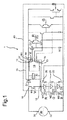
図1は、本発明による回路装置1を示している。回路装置1は、制御回路10を有し、制御回路10は、エネルギ貯蔵装置としてコンデンサCを有し、制御ユニットとしてマイクロコントローラ13を有する。制御回路10は、バイパスMOSFET M4と並列に接続される。制御回路10及びバイパスMOSFET M4の両方とも、入力端子11と出力端子12との間に接続される。入力端子11は、LEDドライバ(図示せず)によって供給される定電流源30の正端子31に接続される。コンデンサCと入力端子11との間には充電制御ダイオードD4が接続される。
FIG. 1 shows a circuit device 1 according to the invention. The circuit device 1 includes a
出力端子12は、直列に接続される3つの負荷素子20、21、22の最初のものに接続される。各負荷素子20、21、22は、赤色、緑色及び青色のうちの1つのためのLED D1、D2、D3を有する。各負荷素子20、21、22の構成は同一であることから、第1負荷素子20だけ詳細に説明する。ここで、第1LED D1は、分流スイッチとしての役割を果たす第1MOSFET M1に並列に接続される。LEDドライバによって供給される一定の電流は、第1LED D1と第1MOSFET M1との間で分けられ、第1MOSFET M1を流れる電流が増加する場合に、第1LED D1の電力消費は減少するだろう。
The
第1MOSFET M1は、マイクロコントローラ13により第1操作端子14を用いて操作される。第1操作端子14は、第1抵抗器R1を通して、PNP型トランジスタである第1トランジスタQ1のベースに接続される。第1トランジスタQ1のエミッタは、充電制御ダイオードD4に接続され、第1トランジスタQ1のコレクタは、NPN型トランジスタである第2トランジスタQ2のベース、及びPNP型トランジスタである第3トランジスタQ3のベースに接続され、且つ第2抵抗器R2を通して定電流源30の負端子32に接続される。第2トランジスタQ2のエミッタは、充電制御ダイオードD4に接続され、第2トランジスタQ2のコレクタは、第3トランジスタQ3のエミッタに接続される。第3トランジスタQ3のコレクタは、負端子32に接続される。
第2トランジスタQ2のコレクタ(及び第3トランジスタQ3のエミッタ)は、第3抵抗器R3を通して、第1MOSFET M1のゲートに接続される。マイクロコントローラ13は、各々、第2及び第3MOSFET M2、M3を操作するための、第2及び第3操作端子15、16も有する。第2及び第3操作端子15、16は、第1操作端子に対応するようにして、抵抗器及びトランジスタのセットに接続される。
The first MOSFET M1 is operated by the
The collector of the second transistor Q2 (and the emitter of the third transistor Q3) is connected to the gate of the first MOSFET M1 through the third resistor R3. The
更に、マイクロコントローラ13は、第4抵抗器R4を通してバイパスMOSFET M4のゲートに接続されるバイパス操作端子17を有する。マイクロコントローラ13は、コンデンサCにおける電圧を検出し、内部比較器回路(図示せず)を用いて、前記電圧を、上方しきい値及び下方しきい値と比較する。
Furthermore, the
動作中、電流源30は、正端子31に一定の電流を供給する。最初の電源投入時、バイパスMOSFET M4はオフに切り替えられる。従って、一定の電流は、マイクロコントローラ13を通過し、コンデンサCを充電する。コンデンサCは、上方しきい値に到達するまで充電される。この時点において、マイクロコントローラ13は、バイパスMOSFET M4をオンに切り替える。ここで、電流源30の電流は、バイパスMOSFET M4を通って、直接、LED D1、D2、D3及び/又は分流スイッチM1、M2、M3へ行くだろう。この状態においては、電流源30からの電流は、制御回路10に全く(又はごくわずかしか)流れ込まない。それ故、マイクロコントローラ13は、コンデンサCによって給電され、これは、コンデンサCの電圧を低下させる。コンデンサCの下方しきい値電圧に到達すると、マイクロコントローラ13は、バイパスMOSFET M4をオフに切り替え、充電プロセスが、再び、開始される。LED D1、D2、D3の上に電源を配置することによって、ゲート駆動電圧は、バイパスMOSFET M4を切り替えるのに十分である。ゲート駆動電圧は、常に、最も高いLED順電圧より高いので、この浮遊/ハイ側電源は、分流スイッチングもサポートする。
During operation, the
マイクロコントローラは、更に、第1、第2及び第3LED D1、D2、D3の光出力を、対応するMOSFET M1、M2、M3を操作することによって、制御する。一例として、第1MOSFET M1の動作を以下に記載する。 The microcontroller further controls the light output of the first, second and third LEDs D1, D2, D3 by manipulating the corresponding MOSFETs M1, M2, M3. As an example, the operation of the first MOSFET M1 will be described below.
マイクロコントローラ13が、第1操作端子14の電圧を低い値に設定するとき、電流は、第1トランジスタQ1のエミッタから、第1トランジスタQ1のベースを通り、第1抵抗器R1を介して、マイクロコントローラ13の方へ流れ始める。第1トランジスタQ1が、オンに切り替えられ、第1トランジスタQ1のコレクタの電圧が、増加し始める。第1トランジスタQ1のコレクタ電圧が十分になるとき、それは、第2トランジスタQ2のベースへの電流供給を開始し、第2トランジスタQ2は、オンへ切り替わり始めるだろう。第2トランジスタQ2のエミッタ電圧は、第2トランジスタQ2のコレクタ電圧へと上昇する。この期間中、第1MOSFET M1のゲート電圧が、増加し始め、最終的に、第1MOSFET M1は、オンへ切り替わる。
When the
第1MOSFET M1をオフに切り替えるため、第1操作端子14の電圧が、高く設定される。第1トランジスタQ1のベース−エミッタ電圧は、低下し、第1トランジスタQ1をオフに切り替わらせる。第1トランジスタQ1がオフに切り替えられると、第2抵抗器R2が、第2及び第3トランジスタQ2、Q3のベース電圧を引き下げるだろう。第2トランジスタQ2は閉じ、第3トランジスタQ3は導通を開始するだろう。次いで、第1MOSFET M1のゲートが、第3抵抗器R3及び第3トランジスタQ3を介して(並びに、非常にわずかに、第3トランジスタQ3のベース及び第2抵抗器R2を通して)、放電されるだろう。MOSFET M1は、オフに切り替えられるだろう。
In order to switch off the first MOSFET M1, the voltage of the
制御は、所定の時間パターンに従い得る。しかしながら、マイクロコントローラ13はまた、ZigBeeネットワーク装置の一部であり得る。この場合には、ユーザは、或るRGBの色を選択するためにZigBee準拠遠隔制御装置(図示せず)を用いることができる。遠隔制御装置は、対応するコマンドをマクロコントローラ13に送信し、マイクロコントローラ13は、それに応じて、MOSFET M1、M2、M3を操作する。ZigBeeネットワーク装置全体が、マイクロコントローラ13と同じように、即ち、定電流源30及びコンデンサCによって、給電され得る。従って、付加的な電源の必要性なしに、ZigBeeの機能をLEDランプに組み込むことが可能である。前述のように、ZigBeeの代わりに他の機能、例えばWiFiも付加されることができ、又はマイクロコントローラ13は、運動センサ、タッチセンサなどに接続されることができる。これらのアプリケーションの各々において、付加的な機能のために付加的な電源は必要とされない。
Control may follow a predetermined time pattern. However, the
図1に示されている回路装置は、電流源と、(負荷素子から成る)負荷と、供給及び制御回路40とに分けられ得る(図1参照)。後者は、既存照明器具のためのレトロフィット組立体として用いられ得る。それによって、ランプ全体を交換する必要なく、新しい制御特徴及び機能が付加され得る。利点は、補助電源が必要なく、全ての配線調節がLEDドライバ30の低電圧側でなされることができ、それによって、修正を安全の観点で害のないものにすることである。
The circuit arrangement shown in FIG. 1 can be divided into a current source, a load (consisting of load elements), and a supply and control circuit 40 (see FIG. 1). The latter can be used as a retrofit assembly for existing luminaires. Thereby, new control features and functions can be added without having to replace the entire lamp. The advantage is that no auxiliary power is required and all wiring adjustments can be made on the low voltage side of the
図2は、供給及び制御回路40がどのようにシステムレベルにおけるアドオンユニットとして用いられ得るかの例を示している。示されているのは、LEDランプの構成要素である。LEDドライバ30は、電源の活線(live wire)50及び中性線(neutral wire)51に接続される。レトロフィット組立体41の一部としての供給及び制御回路40は、LEDドライバ30の低電圧側に接続され得る。上述の新しい特徴(ZigBee又はWiFi機能など)のいずれも、レトロフィット組立体41に組み込まれる。供給及び制御回路40は、(簡単にするために、対応する分流スイッチなしにLEDだけが示されている)負荷23に接続され、負荷23は、供給及び制御回路40に組み込まれる制御ユニット10によって制御される。図2に示されているように、本発明の回路装置1は、分流スイッチングを可能にする任意の商品LEDドライバ30を用いる照明器具に制御特徴を付加するビルディングブロックとして用いられ得る。これは、在庫の構成要素をより少なくすること、及び既存の照明器具に対する新しい機能の付加の容易化をもたらす。
FIG. 2 shows an example of how the supply and
図面、明細及び添付の特許請求の範囲から請求項記載の発明を実施する当業者には、開示されている実施例に対する他の変形が、理解され、達成され得る。 Other variations to the disclosed embodiments can be understood and attained by those skilled in the art from the drawings, the specification, and the appended claims, implementing the claimed invention.
上記の記載及び添付の特許請求の範囲において、単数形への言及は、複数形も含むよう意図されており、その逆もまた同じであり、特定の個数の特徴又は装置への言及は、本発明を特定の個数の特徴又は装置に限定するように解釈されべきではない。更に、「含む」又は「有する」などの表現は、他の要素を除外せず、単数形表記は、複数性を除外しない。 In the above description and in the appended claims, references to the singular are intended to include the plural and vice versa, and references to a particular number of features or devices are The invention should not be construed as limited to a particular number of features or apparatus. Furthermore, expressions such as “include” or “have” do not exclude other elements, and singular notation excludes pluralities.
単に、特定の手段が、相互に異なる従属請求項において引用されているという事実は、これらの手段の組み合わせが有利になるように用いられることができないことを示すものではない。請求項における如何なる参照符号も、請求項の範囲を限定するものとして解釈されるべきではない。 The mere fact that certain measures are recited in mutually different dependent claims does not indicate that a combination of these measures cannot be used to advantage. Any reference signs in the claims should not be construed as limiting the scope.
Claims (14)
電源との接続のための入力端子と、
負荷を有する少なくとも1つの回路との接続のための出力端子と、
制御回路であって、
前記少なくとも1つの回路を制御するよう適応される制御装置、及び
前記制御装置に電力を供給するよう適応されるエネルギ貯蔵装置を含む制御回路と、
制御可能なバイパススイッチとを有する回路装置であって、
前記バイパススイッチ及び前記制御回路が、並列に接続され、前記入力端子と前記出力端子との間に接続され、
前記回路装置が、前記制御回路に供給される電力を制御するよう前記バイパススイッチを動作させるよう適応される回路装置。 A circuit arrangement for controlling at least one load, at least,
An input terminal for connection to a power source;
An output terminal for connection with at least one circuit having a load;
A control circuit,
A control device adapted to control the at least one circuit ; and a control circuit comprising an energy storage device adapted to supply power to the control device;
A circuit device having a controllable bypass switch,
The bypass switch and the control circuit are connected in parallel, connected between the input terminal and the output terminal,
The circuit device is adapted to operate the bypass switch to control power supplied to the control circuit.
負荷ユニットと、
分流装置とを有し、
前記負荷ユニット及び前記分流装置が、前記出力端子に対して、互いに並列に接続される請求項11に記載の回路装置。 A circuit having the load,
A load unit;
A shunt device;
The circuit device according to claim 11, wherein the load unit and the shunt device are connected in parallel to the output terminal.
電源との接続のための入力端子と、
負荷を有する少なくとも1つの回路との接続のための出力端子と、
制御回路であって、
制御装置、及び
エネルギ貯蔵装置を含む制御回路と、
制御可能なバイパススイッチとを有し、
前記バイパススイッチ及び前記制御回路が、並列に接続され、前記入力端子と前記出力端子との間に接続され、
前記制御装置が、負荷を有する少なくとも1つの回路を制御し、
前記エネルギ貯蔵装置が、前記制御装置に電力を供給し、
前記回路装置が、前記制御回路に供給される電力を制御するよう前記バイパススイッチを動作させる方法。 A method of controlling at least one load with a circuit device, the circuit device comprising:
An input terminal for connection to a power source;
An output terminal for connection with at least one circuit having a load;
A control circuit,
A control circuit including a control device and an energy storage device;
A controllable bypass switch,
The bypass switch and the control circuit are connected in parallel, connected between the input terminal and the output terminal,
The controller controls at least one circuit having a load;
The energy storage device supplies power to the control device;
A method in which the circuit device operates the bypass switch to control power supplied to the control circuit.
Applications Claiming Priority (5)
| Application Number | Priority Date | Filing Date | Title |
|---|---|---|---|
| US201261613121P | 2012-03-20 | 2012-03-20 | |
| US61/613,121 | 2012-03-20 | ||
| US201261726624P | 2012-11-15 | 2012-11-15 | |
| US61/726,624 | 2012-11-15 | ||
| PCT/IB2013/051841 WO2013150399A1 (en) | 2012-03-20 | 2013-03-08 | Led string driver circuit including a charge control diode for a capacitor |
Publications (2)
| Publication Number | Publication Date |
|---|---|
| JP2015516648A JP2015516648A (en) | 2015-06-11 |
| JP6243397B2 true JP6243397B2 (en) | 2017-12-06 |
Family
ID=48326354
Family Applications (1)
| Application Number | Title | Priority Date | Filing Date |
|---|---|---|---|
| JP2015501013A Active JP6243397B2 (en) | 2012-03-20 | 2013-03-08 | LED string drive circuit including charge control diode for capacitor |
Country Status (7)
| Country | Link |
|---|---|
| US (1) | US9326340B2 (en) |
| EP (1) | EP2829158B1 (en) |
| JP (1) | JP6243397B2 (en) |
| CN (1) | CN104322145B (en) |
| BR (1) | BR112014023013B1 (en) |
| RU (1) | RU2644562C2 (en) |
| WO (1) | WO2013150399A1 (en) |
Families Citing this family (10)
| Publication number | Priority date | Publication date | Assignee | Title |
|---|---|---|---|---|
| US20150022087A1 (en) | 2013-07-16 | 2015-01-22 | GE Lighting Solutions, LLC | Method and apparatus for providing supplemental power in a led driver |
| JP6646645B2 (en) * | 2014-07-17 | 2020-02-14 | シグニファイ ホールディング ビー ヴィSignify Holding B.V. | Lighting equipment |
| GB2531080A (en) * | 2014-10-06 | 2016-04-13 | Tridonic Gmbh & Co Kg | Emergency lighting unit |
| US10624159B2 (en) * | 2015-03-17 | 2020-04-14 | Signify Holding B.V. | Driver with at least four different states |
| CN106028513B (en) * | 2016-06-03 | 2018-06-26 | 杭州荣亚科技有限公司 | A kind of intelligent dimming controller suitable for the light modulation of large area space place |
| WO2018054841A1 (en) * | 2016-09-22 | 2018-03-29 | Philips Lighting Holding B.V. | A retrofit light emitting diode, led, tube for enabling step dimming in a multi lamp luminaire lighting system |
| ES2939737T3 (en) * | 2018-07-17 | 2023-04-26 | Siemens Energy Global Gmbh & Co Kg | Procedure for operation of a controllable electrical device and arrangement with the controllable electrical device |
| JP7042444B2 (en) * | 2018-07-27 | 2022-03-28 | パナソニックIpマネジメント株式会社 | Load control system |
| CN110572897B (en) * | 2019-08-20 | 2024-03-19 | 深圳市晟碟半导体有限公司 | High-power-factor stroboflash-free LED dimming circuit, device and dimming method |
| CN115776752B (en) * | 2023-02-13 | 2023-08-04 | 佛山市银河兰晶科技股份有限公司 | Control circuit, lamp and control method based on ZigBee protocol |
Family Cites Families (16)
| Publication number | Priority date | Publication date | Assignee | Title |
|---|---|---|---|---|
| US3890555A (en) | 1973-09-06 | 1975-06-17 | Kel Lite Industries | Battery recharging circuit with indicator lights |
| WO2007035883A2 (en) * | 2005-09-20 | 2007-03-29 | California Micro Devices Corporation | Driving parallel strings of series connected leds |
| WO2008060469A2 (en) * | 2006-11-10 | 2008-05-22 | Philips Solid-State Lighting Solutions, Inc. | Methods and apparatus for controlling series-connected leds |
| JP2009004483A (en) * | 2007-06-20 | 2009-01-08 | Sharp Corp | Light-emitting diode drive circuit |
| US7859501B2 (en) * | 2007-06-22 | 2010-12-28 | Global Oled Technology Llc | OLED display with aging and efficiency compensation |
| JP5337153B2 (en) * | 2007-07-02 | 2013-11-06 | コーニンクレッカ フィリップス エヌ ヴェ | Driving device for load and method for driving load using such driving device |
| WO2009013675A1 (en) | 2007-07-23 | 2009-01-29 | Nxp B.V. | Self-powered led bypass-switch configuration |
| US8587217B2 (en) * | 2007-08-24 | 2013-11-19 | Cirrus Logic, Inc. | Multi-LED control |
| JP5065188B2 (en) | 2008-05-23 | 2012-10-31 | オリジン電気株式会社 | Series resonant converter |
| WO2010063001A1 (en) * | 2008-11-26 | 2010-06-03 | Wireless Environment, Llc | Wireless lighting devices and applications |
| US8174212B2 (en) * | 2008-11-30 | 2012-05-08 | Microsemi Corp.—Analog Mixed Signal Group Ltd. | LED string driver with light intensity responsive to input voltage |
| US10264637B2 (en) | 2009-09-24 | 2019-04-16 | Cree, Inc. | Solid state lighting apparatus with compensation bypass circuits and methods of operation thereof |
| JP2011142719A (en) * | 2010-01-06 | 2011-07-21 | Sharp Corp | Switching power supply device |
| NL2004458C2 (en) | 2010-03-25 | 2011-09-27 | Eldolab Holding Bv | Led driver operating in boundary condition mode. |
| TWI434599B (en) * | 2010-07-23 | 2014-04-11 | Advanced Connectek Inc | A light-emitting element driving circuit |
| US9295124B2 (en) * | 2010-07-30 | 2016-03-22 | Infineon Technologies Americas Corp. | System using shunt circuits to selectively bypass open loads |
-
2013
- 2013-03-08 EP EP13721393.0A patent/EP2829158B1/en active Active
- 2013-03-08 CN CN201380015522.2A patent/CN104322145B/en active Active
- 2013-03-08 US US14/385,776 patent/US9326340B2/en active Active
- 2013-03-08 WO PCT/IB2013/051841 patent/WO2013150399A1/en active Application Filing
- 2013-03-08 BR BR112014023013-7A patent/BR112014023013B1/en active IP Right Grant
- 2013-03-08 RU RU2014142062A patent/RU2644562C2/en active
- 2013-03-08 JP JP2015501013A patent/JP6243397B2/en active Active
Also Published As
| Publication number | Publication date |
|---|---|
| RU2644562C2 (en) | 2018-02-13 |
| BR112014023013B1 (en) | 2021-05-18 |
| JP2015516648A (en) | 2015-06-11 |
| EP2829158B1 (en) | 2016-05-18 |
| CN104322145A (en) | 2015-01-28 |
| WO2013150399A1 (en) | 2013-10-10 |
| CN104322145B (en) | 2017-04-26 |
| RU2014142062A (en) | 2016-05-10 |
| US9326340B2 (en) | 2016-04-26 |
| US20150042230A1 (en) | 2015-02-12 |
| EP2829158A1 (en) | 2015-01-28 |
Similar Documents
| Publication | Publication Date | Title |
|---|---|---|
| JP6243397B2 (en) | LED string drive circuit including charge control diode for capacitor | |
| US10728993B2 (en) | Driver circuit for providing constant voltage to an auxiliary circuit | |
| TWI478625B (en) | Dimming controllers, driving circuits and driving methods for driving light source | |
| CN201682668U (en) | Power supply with light adjusting function for LED (light-emitting diode) lamp | |
| JP6430665B2 (en) | LED driver and driving method | |
| US10362644B1 (en) | Flyback converter with load condition control circuit | |
| US10243473B1 (en) | Gate drive IC with adaptive operating mode | |
| TW201519695A (en) | Light source driving circuit, color temperature controller and method for controlling color temperature of light source | |
| EP2786640B1 (en) | Driver circuit for at least one load and method of operating the same | |
| CN102638921A (en) | Lighting device for semiconductor light emitting elements and illumination apparatus including the same | |
| KR101536108B1 (en) | Control circuit and voltage generating method for led lighting apparatus | |
| KR101043476B1 (en) | Pwm dimming driving circuit for led | |
| JP6011011B2 (en) | Lighting device, lighting device, and dimming method | |
| JP2010257026A (en) | Power supply circuit and illuminator | |
| KR101518554B1 (en) | Power supplies to drive the multiple LED modules and the lighting apparatus including the same | |
| US11602028B2 (en) | LED device and lighting device including the same | |
| EP2503850B1 (en) | Illumination fixture | |
| JP2012038781A (en) | Light-emitting element drive circuit and display device | |
| GB2520425A (en) | Circuits and methods for driving light sources | |
| JP2020517071A5 (en) | ||
| CN105517275A (en) | A driving circuit, a dimming controller and a method for adjusting power of a light source | |
| US20200015333A1 (en) | Lighting device, system and method for controlling a lighting device | |
| CN108337762B (en) | Control circuit and LED lighting device | |
| KR20170100912A (en) | Lighting apparatus |
Legal Events
| Date | Code | Title | Description |
|---|---|---|---|
| RD02 | Notification of acceptance of power of attorney |
Free format text: JAPANESE INTERMEDIATE CODE: A7422 Effective date: 20151005 |
|
| A621 | Written request for application examination |
Free format text: JAPANESE INTERMEDIATE CODE: A621 Effective date: 20160302 |
|
| A711 | Notification of change in applicant |
Free format text: JAPANESE INTERMEDIATE CODE: A711 Effective date: 20160330 |
|
| RD02 | Notification of acceptance of power of attorney |
Free format text: JAPANESE INTERMEDIATE CODE: A7422 Effective date: 20160408 |
|
| RD04 | Notification of resignation of power of attorney |
Free format text: JAPANESE INTERMEDIATE CODE: A7424 Effective date: 20160418 |
|
| A977 | Report on retrieval |
Free format text: JAPANESE INTERMEDIATE CODE: A971007 Effective date: 20170119 |
|
| A131 | Notification of reasons for refusal |
Free format text: JAPANESE INTERMEDIATE CODE: A131 Effective date: 20170202 |
|
| A521 | Request for written amendment filed |
Free format text: JAPANESE INTERMEDIATE CODE: A523 Effective date: 20170419 |
|
| RD02 | Notification of acceptance of power of attorney |
Free format text: JAPANESE INTERMEDIATE CODE: A7422 Effective date: 20170515 |
|
| RD04 | Notification of resignation of power of attorney |
Free format text: JAPANESE INTERMEDIATE CODE: A7424 Effective date: 20170609 |
|
| A131 | Notification of reasons for refusal |
Free format text: JAPANESE INTERMEDIATE CODE: A131 Effective date: 20170725 |
|
| A521 | Request for written amendment filed |
Free format text: JAPANESE INTERMEDIATE CODE: A523 Effective date: 20171010 |
|
| TRDD | Decision of grant or rejection written | ||
| A01 | Written decision to grant a patent or to grant a registration (utility model) |
Free format text: JAPANESE INTERMEDIATE CODE: A01 Effective date: 20171020 |
|
| A61 | First payment of annual fees (during grant procedure) |
Free format text: JAPANESE INTERMEDIATE CODE: A61 Effective date: 20171109 |
|
| R150 | Certificate of patent or registration of utility model |
Ref document number: 6243397 Country of ref document: JP Free format text: JAPANESE INTERMEDIATE CODE: R150 |
|
| S531 | Written request for registration of change of domicile |
Free format text: JAPANESE INTERMEDIATE CODE: R313531 |
|
| S533 | Written request for registration of change of name |
Free format text: JAPANESE INTERMEDIATE CODE: R313533 |
|
| R350 | Written notification of registration of transfer |
Free format text: JAPANESE INTERMEDIATE CODE: R350 |
|
| R250 | Receipt of annual fees |
Free format text: JAPANESE INTERMEDIATE CODE: R250 |
|
| R250 | Receipt of annual fees |
Free format text: JAPANESE INTERMEDIATE CODE: R250 |
|
| R250 | Receipt of annual fees |
Free format text: JAPANESE INTERMEDIATE CODE: R250 |