JP6242231B2 - Semiconductor device and manufacturing method thereof - Google Patents
Semiconductor device and manufacturing method thereof Download PDFInfo
- Publication number
- JP6242231B2 JP6242231B2 JP2014024242A JP2014024242A JP6242231B2 JP 6242231 B2 JP6242231 B2 JP 6242231B2 JP 2014024242 A JP2014024242 A JP 2014024242A JP 2014024242 A JP2014024242 A JP 2014024242A JP 6242231 B2 JP6242231 B2 JP 6242231B2
- Authority
- JP
- Japan
- Prior art keywords
- semiconductor chip
- underfill resin
- resin
- chip
- semiconductor
- Prior art date
- Legal status (The legal status is an assumption and is not a legal conclusion. Google has not performed a legal analysis and makes no representation as to the accuracy of the status listed.)
- Active
Links
- 239000004065 semiconductor Substances 0.000 title claims description 296
- 238000004519 manufacturing process Methods 0.000 title claims description 33
- 229920005989 resin Polymers 0.000 claims description 205
- 239000011347 resin Substances 0.000 claims description 205
- 239000000463 material Substances 0.000 claims description 69
- 238000007789 sealing Methods 0.000 claims description 65
- 239000000758 substrate Substances 0.000 claims description 50
- 238000000034 method Methods 0.000 claims description 27
- NJPPVKZQTLUDBO-UHFFFAOYSA-N novaluron Chemical compound C1=C(Cl)C(OC(F)(F)C(OC(F)(F)F)F)=CC=C1NC(=O)NC(=O)C1=C(F)C=CC=C1F NJPPVKZQTLUDBO-UHFFFAOYSA-N 0.000 claims description 24
- 239000002356 single layer Substances 0.000 claims description 5
- 239000011248 coating agent Substances 0.000 claims description 4
- 238000000576 coating method Methods 0.000 claims description 4
- 238000003825 pressing Methods 0.000 claims description 3
- 239000000155 melt Substances 0.000 claims description 2
- 239000010410 layer Substances 0.000 description 59
- 229910000679 solder Inorganic materials 0.000 description 21
- 239000003822 epoxy resin Substances 0.000 description 11
- 229920000647 polyepoxide Polymers 0.000 description 11
- 230000000873 masking effect Effects 0.000 description 10
- 230000015572 biosynthetic process Effects 0.000 description 9
- RYGMFSIKBFXOCR-UHFFFAOYSA-N Copper Chemical compound [Cu] RYGMFSIKBFXOCR-UHFFFAOYSA-N 0.000 description 7
- 229910052802 copper Inorganic materials 0.000 description 7
- 239000010949 copper Substances 0.000 description 7
- 238000002161 passivation Methods 0.000 description 6
- 229910000881 Cu alloy Inorganic materials 0.000 description 5
- XUIMIQQOPSSXEZ-UHFFFAOYSA-N Silicon Chemical compound [Si] XUIMIQQOPSSXEZ-UHFFFAOYSA-N 0.000 description 5
- 239000011229 interlayer Substances 0.000 description 5
- 230000002093 peripheral effect Effects 0.000 description 5
- 238000007747 plating Methods 0.000 description 5
- 229920001721 polyimide Polymers 0.000 description 5
- 229910052710 silicon Inorganic materials 0.000 description 5
- 239000010703 silicon Substances 0.000 description 5
- PXHVJJICTQNCMI-UHFFFAOYSA-N Nickel Chemical compound [Ni] PXHVJJICTQNCMI-UHFFFAOYSA-N 0.000 description 4
- 239000000945 filler Substances 0.000 description 4
- 238000010438 heat treatment Methods 0.000 description 4
- 239000009719 polyimide resin Substances 0.000 description 4
- 239000004925 Acrylic resin Substances 0.000 description 3
- 229920000178 Acrylic resin Polymers 0.000 description 3
- 229910052581 Si3N4 Inorganic materials 0.000 description 3
- VYPSYNLAJGMNEJ-UHFFFAOYSA-N Silicium dioxide Chemical compound O=[Si]=O VYPSYNLAJGMNEJ-UHFFFAOYSA-N 0.000 description 3
- 239000012790 adhesive layer Substances 0.000 description 3
- 230000035515 penetration Effects 0.000 description 3
- HQVNEWCFYHHQES-UHFFFAOYSA-N silicon nitride Chemical compound N12[Si]34N5[Si]62N3[Si]51N64 HQVNEWCFYHHQES-UHFFFAOYSA-N 0.000 description 3
- 229910052814 silicon oxide Inorganic materials 0.000 description 3
- XKRFYHLGVUSROY-UHFFFAOYSA-N Argon Chemical compound [Ar] XKRFYHLGVUSROY-UHFFFAOYSA-N 0.000 description 2
- 230000006866 deterioration Effects 0.000 description 2
- 238000005516 engineering process Methods 0.000 description 2
- PCHJSUWPFVWCPO-UHFFFAOYSA-N gold Chemical compound [Au] PCHJSUWPFVWCPO-UHFFFAOYSA-N 0.000 description 2
- 229910052737 gold Inorganic materials 0.000 description 2
- 239000010931 gold Substances 0.000 description 2
- 230000017525 heat dissipation Effects 0.000 description 2
- 239000007788 liquid Substances 0.000 description 2
- 229910052759 nickel Inorganic materials 0.000 description 2
- 239000004642 Polyimide Substances 0.000 description 1
- 229910004298 SiO 2 Inorganic materials 0.000 description 1
- 239000000853 adhesive Substances 0.000 description 1
- 230000001070 adhesive effect Effects 0.000 description 1
- 229910045601 alloy Inorganic materials 0.000 description 1
- 239000000956 alloy Substances 0.000 description 1
- XAGFODPZIPBFFR-UHFFFAOYSA-N aluminium Chemical compound [Al] XAGFODPZIPBFFR-UHFFFAOYSA-N 0.000 description 1
- 229910052782 aluminium Inorganic materials 0.000 description 1
- 229910052786 argon Inorganic materials 0.000 description 1
- 239000003990 capacitor Substances 0.000 description 1
- 230000007423 decrease Effects 0.000 description 1
- 230000007547 defect Effects 0.000 description 1
- 238000002474 experimental method Methods 0.000 description 1
- 239000011521 glass Substances 0.000 description 1
- 239000011810 insulating material Substances 0.000 description 1
- 238000009413 insulation Methods 0.000 description 1
- 230000009545 invasion Effects 0.000 description 1
- 238000005304 joining Methods 0.000 description 1
- 238000003475 lamination Methods 0.000 description 1
- 238000012986 modification Methods 0.000 description 1
- 230000004048 modification Effects 0.000 description 1
- 238000000465 moulding Methods 0.000 description 1
- 230000000149 penetrating effect Effects 0.000 description 1
- XLYOFNOQVPJJNP-UHFFFAOYSA-N water Substances O XLYOFNOQVPJJNP-UHFFFAOYSA-N 0.000 description 1
Images


Classifications
-
- H—ELECTRICITY
- H01—ELECTRIC ELEMENTS
- H01L—SEMICONDUCTOR DEVICES NOT COVERED BY CLASS H10
- H01L25/00—Assemblies consisting of a plurality of individual semiconductor or other solid state devices ; Multistep manufacturing processes thereof
- H01L25/03—Assemblies consisting of a plurality of individual semiconductor or other solid state devices ; Multistep manufacturing processes thereof all the devices being of a type provided for in the same subgroup of groups H01L27/00 - H01L33/00, or in a single subclass of H10K, H10N, e.g. assemblies of rectifier diodes
- H01L25/04—Assemblies consisting of a plurality of individual semiconductor or other solid state devices ; Multistep manufacturing processes thereof all the devices being of a type provided for in the same subgroup of groups H01L27/00 - H01L33/00, or in a single subclass of H10K, H10N, e.g. assemblies of rectifier diodes the devices not having separate containers
- H01L25/065—Assemblies consisting of a plurality of individual semiconductor or other solid state devices ; Multistep manufacturing processes thereof all the devices being of a type provided for in the same subgroup of groups H01L27/00 - H01L33/00, or in a single subclass of H10K, H10N, e.g. assemblies of rectifier diodes the devices not having separate containers the devices being of a type provided for in group H01L27/00
- H01L25/0657—Stacked arrangements of devices
-
- H—ELECTRICITY
- H01—ELECTRIC ELEMENTS
- H01L—SEMICONDUCTOR DEVICES NOT COVERED BY CLASS H10
- H01L21/00—Processes or apparatus adapted for the manufacture or treatment of semiconductor or solid state devices or of parts thereof
- H01L21/02—Manufacture or treatment of semiconductor devices or of parts thereof
- H01L21/04—Manufacture or treatment of semiconductor devices or of parts thereof the devices having potential barriers, e.g. a PN junction, depletion layer or carrier concentration layer
- H01L21/50—Assembly of semiconductor devices using processes or apparatus not provided for in a single one of the subgroups H01L21/06 - H01L21/326, e.g. sealing of a cap to a base of a container
- H01L21/56—Encapsulations, e.g. encapsulation layers, coatings
- H01L21/563—Encapsulation of active face of flip-chip device, e.g. underfilling or underencapsulation of flip-chip, encapsulation preform on chip or mounting substrate
-
- H—ELECTRICITY
- H01—ELECTRIC ELEMENTS
- H01L—SEMICONDUCTOR DEVICES NOT COVERED BY CLASS H10
- H01L25/00—Assemblies consisting of a plurality of individual semiconductor or other solid state devices ; Multistep manufacturing processes thereof
- H01L25/50—Multistep manufacturing processes of assemblies consisting of devices, each device being of a type provided for in group H01L27/00 or H01L29/00
-
- H—ELECTRICITY
- H05—ELECTRIC TECHNIQUES NOT OTHERWISE PROVIDED FOR
- H05K—PRINTED CIRCUITS; CASINGS OR CONSTRUCTIONAL DETAILS OF ELECTRIC APPARATUS; MANUFACTURE OF ASSEMBLAGES OF ELECTRICAL COMPONENTS
- H05K3/00—Apparatus or processes for manufacturing printed circuits
- H05K3/36—Assembling printed circuits with other printed circuits
- H05K3/368—Assembling printed circuits with other printed circuits parallel to each other
-
- H—ELECTRICITY
- H01—ELECTRIC ELEMENTS
- H01L—SEMICONDUCTOR DEVICES NOT COVERED BY CLASS H10
- H01L2224/00—Indexing scheme for arrangements for connecting or disconnecting semiconductor or solid-state bodies and methods related thereto as covered by H01L24/00
- H01L2224/01—Means for bonding being attached to, or being formed on, the surface to be connected, e.g. chip-to-package, die-attach, "first-level" interconnects; Manufacturing methods related thereto
- H01L2224/02—Bonding areas; Manufacturing methods related thereto
- H01L2224/04—Structure, shape, material or disposition of the bonding areas prior to the connecting process
- H01L2224/0401—Bonding areas specifically adapted for bump connectors, e.g. under bump metallisation [UBM]
-
- H—ELECTRICITY
- H01—ELECTRIC ELEMENTS
- H01L—SEMICONDUCTOR DEVICES NOT COVERED BY CLASS H10
- H01L2224/00—Indexing scheme for arrangements for connecting or disconnecting semiconductor or solid-state bodies and methods related thereto as covered by H01L24/00
- H01L2224/01—Means for bonding being attached to, or being formed on, the surface to be connected, e.g. chip-to-package, die-attach, "first-level" interconnects; Manufacturing methods related thereto
- H01L2224/10—Bump connectors; Manufacturing methods related thereto
- H01L2224/12—Structure, shape, material or disposition of the bump connectors prior to the connecting process
- H01L2224/13—Structure, shape, material or disposition of the bump connectors prior to the connecting process of an individual bump connector
- H01L2224/13001—Core members of the bump connector
- H01L2224/1302—Disposition
- H01L2224/13022—Disposition the bump connector being at least partially embedded in the surface
-
- H—ELECTRICITY
- H01—ELECTRIC ELEMENTS
- H01L—SEMICONDUCTOR DEVICES NOT COVERED BY CLASS H10
- H01L2224/00—Indexing scheme for arrangements for connecting or disconnecting semiconductor or solid-state bodies and methods related thereto as covered by H01L24/00
- H01L2224/01—Means for bonding being attached to, or being formed on, the surface to be connected, e.g. chip-to-package, die-attach, "first-level" interconnects; Manufacturing methods related thereto
- H01L2224/10—Bump connectors; Manufacturing methods related thereto
- H01L2224/12—Structure, shape, material or disposition of the bump connectors prior to the connecting process
- H01L2224/13—Structure, shape, material or disposition of the bump connectors prior to the connecting process of an individual bump connector
- H01L2224/13001—Core members of the bump connector
- H01L2224/1302—Disposition
- H01L2224/13024—Disposition the bump connector being disposed on a redistribution layer on the semiconductor or solid-state body
-
- H—ELECTRICITY
- H01—ELECTRIC ELEMENTS
- H01L—SEMICONDUCTOR DEVICES NOT COVERED BY CLASS H10
- H01L2224/00—Indexing scheme for arrangements for connecting or disconnecting semiconductor or solid-state bodies and methods related thereto as covered by H01L24/00
- H01L2224/01—Means for bonding being attached to, or being formed on, the surface to be connected, e.g. chip-to-package, die-attach, "first-level" interconnects; Manufacturing methods related thereto
- H01L2224/10—Bump connectors; Manufacturing methods related thereto
- H01L2224/12—Structure, shape, material or disposition of the bump connectors prior to the connecting process
- H01L2224/13—Structure, shape, material or disposition of the bump connectors prior to the connecting process of an individual bump connector
- H01L2224/13001—Core members of the bump connector
- H01L2224/1302—Disposition
- H01L2224/13025—Disposition the bump connector being disposed on a via connection of the semiconductor or solid-state body
-
- H—ELECTRICITY
- H01—ELECTRIC ELEMENTS
- H01L—SEMICONDUCTOR DEVICES NOT COVERED BY CLASS H10
- H01L2224/00—Indexing scheme for arrangements for connecting or disconnecting semiconductor or solid-state bodies and methods related thereto as covered by H01L24/00
- H01L2224/01—Means for bonding being attached to, or being formed on, the surface to be connected, e.g. chip-to-package, die-attach, "first-level" interconnects; Manufacturing methods related thereto
- H01L2224/10—Bump connectors; Manufacturing methods related thereto
- H01L2224/12—Structure, shape, material or disposition of the bump connectors prior to the connecting process
- H01L2224/13—Structure, shape, material or disposition of the bump connectors prior to the connecting process of an individual bump connector
- H01L2224/13001—Core members of the bump connector
- H01L2224/13075—Plural core members
- H01L2224/1308—Plural core members being stacked
- H01L2224/13082—Two-layer arrangements
-
- H—ELECTRICITY
- H01—ELECTRIC ELEMENTS
- H01L—SEMICONDUCTOR DEVICES NOT COVERED BY CLASS H10
- H01L2224/00—Indexing scheme for arrangements for connecting or disconnecting semiconductor or solid-state bodies and methods related thereto as covered by H01L24/00
- H01L2224/01—Means for bonding being attached to, or being formed on, the surface to be connected, e.g. chip-to-package, die-attach, "first-level" interconnects; Manufacturing methods related thereto
- H01L2224/10—Bump connectors; Manufacturing methods related thereto
- H01L2224/12—Structure, shape, material or disposition of the bump connectors prior to the connecting process
- H01L2224/14—Structure, shape, material or disposition of the bump connectors prior to the connecting process of a plurality of bump connectors
- H01L2224/141—Disposition
- H01L2224/1418—Disposition being disposed on at least two different sides of the body, e.g. dual array
- H01L2224/14181—On opposite sides of the body
-
- H—ELECTRICITY
- H01—ELECTRIC ELEMENTS
- H01L—SEMICONDUCTOR DEVICES NOT COVERED BY CLASS H10
- H01L2224/00—Indexing scheme for arrangements for connecting or disconnecting semiconductor or solid-state bodies and methods related thereto as covered by H01L24/00
- H01L2224/01—Means for bonding being attached to, or being formed on, the surface to be connected, e.g. chip-to-package, die-attach, "first-level" interconnects; Manufacturing methods related thereto
- H01L2224/10—Bump connectors; Manufacturing methods related thereto
- H01L2224/15—Structure, shape, material or disposition of the bump connectors after the connecting process
- H01L2224/16—Structure, shape, material or disposition of the bump connectors after the connecting process of an individual bump connector
- H01L2224/161—Disposition
- H01L2224/16135—Disposition the bump connector connecting between different semiconductor or solid-state bodies, i.e. chip-to-chip
- H01L2224/16145—Disposition the bump connector connecting between different semiconductor or solid-state bodies, i.e. chip-to-chip the bodies being stacked
- H01L2224/16146—Disposition the bump connector connecting between different semiconductor or solid-state bodies, i.e. chip-to-chip the bodies being stacked the bump connector connecting to a via connection in the semiconductor or solid-state body
-
- H—ELECTRICITY
- H01—ELECTRIC ELEMENTS
- H01L—SEMICONDUCTOR DEVICES NOT COVERED BY CLASS H10
- H01L2224/00—Indexing scheme for arrangements for connecting or disconnecting semiconductor or solid-state bodies and methods related thereto as covered by H01L24/00
- H01L2224/01—Means for bonding being attached to, or being formed on, the surface to be connected, e.g. chip-to-package, die-attach, "first-level" interconnects; Manufacturing methods related thereto
- H01L2224/10—Bump connectors; Manufacturing methods related thereto
- H01L2224/15—Structure, shape, material or disposition of the bump connectors after the connecting process
- H01L2224/16—Structure, shape, material or disposition of the bump connectors after the connecting process of an individual bump connector
- H01L2224/161—Disposition
- H01L2224/16135—Disposition the bump connector connecting between different semiconductor or solid-state bodies, i.e. chip-to-chip
- H01L2224/16145—Disposition the bump connector connecting between different semiconductor or solid-state bodies, i.e. chip-to-chip the bodies being stacked
- H01L2224/16148—Disposition the bump connector connecting between different semiconductor or solid-state bodies, i.e. chip-to-chip the bodies being stacked the bump connector connecting to a bonding area protruding from the surface
-
- H—ELECTRICITY
- H01—ELECTRIC ELEMENTS
- H01L—SEMICONDUCTOR DEVICES NOT COVERED BY CLASS H10
- H01L2224/00—Indexing scheme for arrangements for connecting or disconnecting semiconductor or solid-state bodies and methods related thereto as covered by H01L24/00
- H01L2224/01—Means for bonding being attached to, or being formed on, the surface to be connected, e.g. chip-to-package, die-attach, "first-level" interconnects; Manufacturing methods related thereto
- H01L2224/10—Bump connectors; Manufacturing methods related thereto
- H01L2224/15—Structure, shape, material or disposition of the bump connectors after the connecting process
- H01L2224/16—Structure, shape, material or disposition of the bump connectors after the connecting process of an individual bump connector
- H01L2224/161—Disposition
- H01L2224/16151—Disposition the bump connector connecting between a semiconductor or solid-state body and an item not being a semiconductor or solid-state body, e.g. chip-to-substrate, chip-to-passive
- H01L2224/16221—Disposition the bump connector connecting between a semiconductor or solid-state body and an item not being a semiconductor or solid-state body, e.g. chip-to-substrate, chip-to-passive the body and the item being stacked
- H01L2224/16225—Disposition the bump connector connecting between a semiconductor or solid-state body and an item not being a semiconductor or solid-state body, e.g. chip-to-substrate, chip-to-passive the body and the item being stacked the item being non-metallic, e.g. insulating substrate with or without metallisation
- H01L2224/16235—Disposition the bump connector connecting between a semiconductor or solid-state body and an item not being a semiconductor or solid-state body, e.g. chip-to-substrate, chip-to-passive the body and the item being stacked the item being non-metallic, e.g. insulating substrate with or without metallisation the bump connector connecting to a via metallisation of the item
-
- H—ELECTRICITY
- H01—ELECTRIC ELEMENTS
- H01L—SEMICONDUCTOR DEVICES NOT COVERED BY CLASS H10
- H01L2224/00—Indexing scheme for arrangements for connecting or disconnecting semiconductor or solid-state bodies and methods related thereto as covered by H01L24/00
- H01L2224/01—Means for bonding being attached to, or being formed on, the surface to be connected, e.g. chip-to-package, die-attach, "first-level" interconnects; Manufacturing methods related thereto
- H01L2224/10—Bump connectors; Manufacturing methods related thereto
- H01L2224/15—Structure, shape, material or disposition of the bump connectors after the connecting process
- H01L2224/16—Structure, shape, material or disposition of the bump connectors after the connecting process of an individual bump connector
- H01L2224/161—Disposition
- H01L2224/16151—Disposition the bump connector connecting between a semiconductor or solid-state body and an item not being a semiconductor or solid-state body, e.g. chip-to-substrate, chip-to-passive
- H01L2224/16221—Disposition the bump connector connecting between a semiconductor or solid-state body and an item not being a semiconductor or solid-state body, e.g. chip-to-substrate, chip-to-passive the body and the item being stacked
- H01L2224/16225—Disposition the bump connector connecting between a semiconductor or solid-state body and an item not being a semiconductor or solid-state body, e.g. chip-to-substrate, chip-to-passive the body and the item being stacked the item being non-metallic, e.g. insulating substrate with or without metallisation
- H01L2224/16238—Disposition the bump connector connecting between a semiconductor or solid-state body and an item not being a semiconductor or solid-state body, e.g. chip-to-substrate, chip-to-passive the body and the item being stacked the item being non-metallic, e.g. insulating substrate with or without metallisation the bump connector connecting to a bonding area protruding from the surface of the item
-
- H—ELECTRICITY
- H01—ELECTRIC ELEMENTS
- H01L—SEMICONDUCTOR DEVICES NOT COVERED BY CLASS H10
- H01L2224/00—Indexing scheme for arrangements for connecting or disconnecting semiconductor or solid-state bodies and methods related thereto as covered by H01L24/00
- H01L2224/01—Means for bonding being attached to, or being formed on, the surface to be connected, e.g. chip-to-package, die-attach, "first-level" interconnects; Manufacturing methods related thereto
- H01L2224/10—Bump connectors; Manufacturing methods related thereto
- H01L2224/15—Structure, shape, material or disposition of the bump connectors after the connecting process
- H01L2224/17—Structure, shape, material or disposition of the bump connectors after the connecting process of a plurality of bump connectors
- H01L2224/171—Disposition
- H01L2224/1718—Disposition being disposed on at least two different sides of the body, e.g. dual array
- H01L2224/17181—On opposite sides of the body
-
- H—ELECTRICITY
- H01—ELECTRIC ELEMENTS
- H01L—SEMICONDUCTOR DEVICES NOT COVERED BY CLASS H10
- H01L2224/00—Indexing scheme for arrangements for connecting or disconnecting semiconductor or solid-state bodies and methods related thereto as covered by H01L24/00
- H01L2224/01—Means for bonding being attached to, or being formed on, the surface to be connected, e.g. chip-to-package, die-attach, "first-level" interconnects; Manufacturing methods related thereto
- H01L2224/26—Layer connectors, e.g. plate connectors, solder or adhesive layers; Manufacturing methods related thereto
- H01L2224/31—Structure, shape, material or disposition of the layer connectors after the connecting process
- H01L2224/32—Structure, shape, material or disposition of the layer connectors after the connecting process of an individual layer connector
- H01L2224/321—Disposition
- H01L2224/32135—Disposition the layer connector connecting between different semiconductor or solid-state bodies, i.e. chip-to-chip
- H01L2224/32145—Disposition the layer connector connecting between different semiconductor or solid-state bodies, i.e. chip-to-chip the bodies being stacked
-
- H—ELECTRICITY
- H01—ELECTRIC ELEMENTS
- H01L—SEMICONDUCTOR DEVICES NOT COVERED BY CLASS H10
- H01L2224/00—Indexing scheme for arrangements for connecting or disconnecting semiconductor or solid-state bodies and methods related thereto as covered by H01L24/00
- H01L2224/01—Means for bonding being attached to, or being formed on, the surface to be connected, e.g. chip-to-package, die-attach, "first-level" interconnects; Manufacturing methods related thereto
- H01L2224/26—Layer connectors, e.g. plate connectors, solder or adhesive layers; Manufacturing methods related thereto
- H01L2224/31—Structure, shape, material or disposition of the layer connectors after the connecting process
- H01L2224/32—Structure, shape, material or disposition of the layer connectors after the connecting process of an individual layer connector
- H01L2224/321—Disposition
- H01L2224/32151—Disposition the layer connector connecting between a semiconductor or solid-state body and an item not being a semiconductor or solid-state body, e.g. chip-to-substrate, chip-to-passive
- H01L2224/32221—Disposition the layer connector connecting between a semiconductor or solid-state body and an item not being a semiconductor or solid-state body, e.g. chip-to-substrate, chip-to-passive the body and the item being stacked
- H01L2224/32225—Disposition the layer connector connecting between a semiconductor or solid-state body and an item not being a semiconductor or solid-state body, e.g. chip-to-substrate, chip-to-passive the body and the item being stacked the item being non-metallic, e.g. insulating substrate with or without metallisation
-
- H—ELECTRICITY
- H01—ELECTRIC ELEMENTS
- H01L—SEMICONDUCTOR DEVICES NOT COVERED BY CLASS H10
- H01L2224/00—Indexing scheme for arrangements for connecting or disconnecting semiconductor or solid-state bodies and methods related thereto as covered by H01L24/00
- H01L2224/01—Means for bonding being attached to, or being formed on, the surface to be connected, e.g. chip-to-package, die-attach, "first-level" interconnects; Manufacturing methods related thereto
- H01L2224/26—Layer connectors, e.g. plate connectors, solder or adhesive layers; Manufacturing methods related thereto
- H01L2224/31—Structure, shape, material or disposition of the layer connectors after the connecting process
- H01L2224/32—Structure, shape, material or disposition of the layer connectors after the connecting process of an individual layer connector
- H01L2224/321—Disposition
- H01L2224/32151—Disposition the layer connector connecting between a semiconductor or solid-state body and an item not being a semiconductor or solid-state body, e.g. chip-to-substrate, chip-to-passive
- H01L2224/32221—Disposition the layer connector connecting between a semiconductor or solid-state body and an item not being a semiconductor or solid-state body, e.g. chip-to-substrate, chip-to-passive the body and the item being stacked
- H01L2224/32245—Disposition the layer connector connecting between a semiconductor or solid-state body and an item not being a semiconductor or solid-state body, e.g. chip-to-substrate, chip-to-passive the body and the item being stacked the item being metallic
-
- H—ELECTRICITY
- H01—ELECTRIC ELEMENTS
- H01L—SEMICONDUCTOR DEVICES NOT COVERED BY CLASS H10
- H01L2224/00—Indexing scheme for arrangements for connecting or disconnecting semiconductor or solid-state bodies and methods related thereto as covered by H01L24/00
- H01L2224/73—Means for bonding being of different types provided for in two or more of groups H01L2224/10, H01L2224/18, H01L2224/26, H01L2224/34, H01L2224/42, H01L2224/50, H01L2224/63, H01L2224/71
- H01L2224/732—Location after the connecting process
- H01L2224/73201—Location after the connecting process on the same surface
- H01L2224/73203—Bump and layer connectors
- H01L2224/73204—Bump and layer connectors the bump connector being embedded into the layer connector
-
- H—ELECTRICITY
- H01—ELECTRIC ELEMENTS
- H01L—SEMICONDUCTOR DEVICES NOT COVERED BY CLASS H10
- H01L2224/00—Indexing scheme for arrangements for connecting or disconnecting semiconductor or solid-state bodies and methods related thereto as covered by H01L24/00
- H01L2224/73—Means for bonding being of different types provided for in two or more of groups H01L2224/10, H01L2224/18, H01L2224/26, H01L2224/34, H01L2224/42, H01L2224/50, H01L2224/63, H01L2224/71
- H01L2224/732—Location after the connecting process
- H01L2224/73251—Location after the connecting process on different surfaces
- H01L2224/73253—Bump and layer connectors
-
- H—ELECTRICITY
- H01—ELECTRIC ELEMENTS
- H01L—SEMICONDUCTOR DEVICES NOT COVERED BY CLASS H10
- H01L2224/00—Indexing scheme for arrangements for connecting or disconnecting semiconductor or solid-state bodies and methods related thereto as covered by H01L24/00
- H01L2224/74—Apparatus for manufacturing arrangements for connecting or disconnecting semiconductor or solid-state bodies and for methods related thereto
- H01L2224/75—Apparatus for connecting with bump connectors or layer connectors
- H01L2224/757—Means for aligning
- H01L2224/75743—Suction holding means
-
- H—ELECTRICITY
- H01—ELECTRIC ELEMENTS
- H01L—SEMICONDUCTOR DEVICES NOT COVERED BY CLASS H10
- H01L2224/00—Indexing scheme for arrangements for connecting or disconnecting semiconductor or solid-state bodies and methods related thereto as covered by H01L24/00
- H01L2224/80—Methods for connecting semiconductor or other solid state bodies using means for bonding being attached to, or being formed on, the surface to be connected
- H01L2224/81—Methods for connecting semiconductor or other solid state bodies using means for bonding being attached to, or being formed on, the surface to be connected using a bump connector
- H01L2224/81001—Methods for connecting semiconductor or other solid state bodies using means for bonding being attached to, or being formed on, the surface to be connected using a bump connector involving a temporary auxiliary member not forming part of the bonding apparatus
- H01L2224/81005—Methods for connecting semiconductor or other solid state bodies using means for bonding being attached to, or being formed on, the surface to be connected using a bump connector involving a temporary auxiliary member not forming part of the bonding apparatus being a temporary or sacrificial substrate
-
- H—ELECTRICITY
- H01—ELECTRIC ELEMENTS
- H01L—SEMICONDUCTOR DEVICES NOT COVERED BY CLASS H10
- H01L2224/00—Indexing scheme for arrangements for connecting or disconnecting semiconductor or solid-state bodies and methods related thereto as covered by H01L24/00
- H01L2224/80—Methods for connecting semiconductor or other solid state bodies using means for bonding being attached to, or being formed on, the surface to be connected
- H01L2224/81—Methods for connecting semiconductor or other solid state bodies using means for bonding being attached to, or being formed on, the surface to be connected using a bump connector
- H01L2224/8119—Arrangement of the bump connectors prior to mounting
- H01L2224/81191—Arrangement of the bump connectors prior to mounting wherein the bump connectors are disposed only on the semiconductor or solid-state body
-
- H—ELECTRICITY
- H01—ELECTRIC ELEMENTS
- H01L—SEMICONDUCTOR DEVICES NOT COVERED BY CLASS H10
- H01L2224/00—Indexing scheme for arrangements for connecting or disconnecting semiconductor or solid-state bodies and methods related thereto as covered by H01L24/00
- H01L2224/80—Methods for connecting semiconductor or other solid state bodies using means for bonding being attached to, or being formed on, the surface to be connected
- H01L2224/81—Methods for connecting semiconductor or other solid state bodies using means for bonding being attached to, or being formed on, the surface to be connected using a bump connector
- H01L2224/8119—Arrangement of the bump connectors prior to mounting
- H01L2224/81193—Arrangement of the bump connectors prior to mounting wherein the bump connectors are disposed on both the semiconductor or solid-state body and another item or body to be connected to the semiconductor or solid-state body
-
- H—ELECTRICITY
- H01—ELECTRIC ELEMENTS
- H01L—SEMICONDUCTOR DEVICES NOT COVERED BY CLASS H10
- H01L2224/00—Indexing scheme for arrangements for connecting or disconnecting semiconductor or solid-state bodies and methods related thereto as covered by H01L24/00
- H01L2224/80—Methods for connecting semiconductor or other solid state bodies using means for bonding being attached to, or being formed on, the surface to be connected
- H01L2224/81—Methods for connecting semiconductor or other solid state bodies using means for bonding being attached to, or being formed on, the surface to be connected using a bump connector
- H01L2224/818—Bonding techniques
- H01L2224/81801—Soldering or alloying
- H01L2224/81815—Reflow soldering
-
- H—ELECTRICITY
- H01—ELECTRIC ELEMENTS
- H01L—SEMICONDUCTOR DEVICES NOT COVERED BY CLASS H10
- H01L2224/00—Indexing scheme for arrangements for connecting or disconnecting semiconductor or solid-state bodies and methods related thereto as covered by H01L24/00
- H01L2224/80—Methods for connecting semiconductor or other solid state bodies using means for bonding being attached to, or being formed on, the surface to be connected
- H01L2224/83—Methods for connecting semiconductor or other solid state bodies using means for bonding being attached to, or being formed on, the surface to be connected using a layer connector
- H01L2224/8319—Arrangement of the layer connectors prior to mounting
- H01L2224/83191—Arrangement of the layer connectors prior to mounting wherein the layer connectors are disposed only on the semiconductor or solid-state body
-
- H—ELECTRICITY
- H01—ELECTRIC ELEMENTS
- H01L—SEMICONDUCTOR DEVICES NOT COVERED BY CLASS H10
- H01L2224/00—Indexing scheme for arrangements for connecting or disconnecting semiconductor or solid-state bodies and methods related thereto as covered by H01L24/00
- H01L2224/80—Methods for connecting semiconductor or other solid state bodies using means for bonding being attached to, or being formed on, the surface to be connected
- H01L2224/83—Methods for connecting semiconductor or other solid state bodies using means for bonding being attached to, or being formed on, the surface to be connected using a layer connector
- H01L2224/8319—Arrangement of the layer connectors prior to mounting
- H01L2224/83192—Arrangement of the layer connectors prior to mounting wherein the layer connectors are disposed only on another item or body to be connected to the semiconductor or solid-state body
-
- H—ELECTRICITY
- H01—ELECTRIC ELEMENTS
- H01L—SEMICONDUCTOR DEVICES NOT COVERED BY CLASS H10
- H01L2224/00—Indexing scheme for arrangements for connecting or disconnecting semiconductor or solid-state bodies and methods related thereto as covered by H01L24/00
- H01L2224/91—Methods for connecting semiconductor or solid state bodies including different methods provided for in two or more of groups H01L2224/80 - H01L2224/90
- H01L2224/92—Specific sequence of method steps
- H01L2224/921—Connecting a surface with connectors of different types
- H01L2224/9212—Sequential connecting processes
- H01L2224/92122—Sequential connecting processes the first connecting process involving a bump connector
- H01L2224/92125—Sequential connecting processes the first connecting process involving a bump connector the second connecting process involving a layer connector
-
- H—ELECTRICITY
- H01—ELECTRIC ELEMENTS
- H01L—SEMICONDUCTOR DEVICES NOT COVERED BY CLASS H10
- H01L2225/00—Details relating to assemblies covered by the group H01L25/00 but not provided for in its subgroups
- H01L2225/03—All the devices being of a type provided for in the same subgroup of groups H01L27/00 - H01L33/648 and H10K99/00
- H01L2225/04—All the devices being of a type provided for in the same subgroup of groups H01L27/00 - H01L33/648 and H10K99/00 the devices not having separate containers
- H01L2225/065—All the devices being of a type provided for in the same subgroup of groups H01L27/00 - H01L33/648 and H10K99/00 the devices not having separate containers the devices being of a type provided for in group H01L27/00
- H01L2225/06503—Stacked arrangements of devices
- H01L2225/06513—Bump or bump-like direct electrical connections between devices, e.g. flip-chip connection, solder bumps
-
- H—ELECTRICITY
- H01—ELECTRIC ELEMENTS
- H01L—SEMICONDUCTOR DEVICES NOT COVERED BY CLASS H10
- H01L2225/00—Details relating to assemblies covered by the group H01L25/00 but not provided for in its subgroups
- H01L2225/03—All the devices being of a type provided for in the same subgroup of groups H01L27/00 - H01L33/648 and H10K99/00
- H01L2225/04—All the devices being of a type provided for in the same subgroup of groups H01L27/00 - H01L33/648 and H10K99/00 the devices not having separate containers
- H01L2225/065—All the devices being of a type provided for in the same subgroup of groups H01L27/00 - H01L33/648 and H10K99/00 the devices not having separate containers the devices being of a type provided for in group H01L27/00
- H01L2225/06503—Stacked arrangements of devices
- H01L2225/06517—Bump or bump-like direct electrical connections from device to substrate
-
- H—ELECTRICITY
- H01—ELECTRIC ELEMENTS
- H01L—SEMICONDUCTOR DEVICES NOT COVERED BY CLASS H10
- H01L2225/00—Details relating to assemblies covered by the group H01L25/00 but not provided for in its subgroups
- H01L2225/03—All the devices being of a type provided for in the same subgroup of groups H01L27/00 - H01L33/648 and H10K99/00
- H01L2225/04—All the devices being of a type provided for in the same subgroup of groups H01L27/00 - H01L33/648 and H10K99/00 the devices not having separate containers
- H01L2225/065—All the devices being of a type provided for in the same subgroup of groups H01L27/00 - H01L33/648 and H10K99/00 the devices not having separate containers the devices being of a type provided for in group H01L27/00
- H01L2225/06503—Stacked arrangements of devices
- H01L2225/06541—Conductive via connections through the device, e.g. vertical interconnects, through silicon via [TSV]
-
- H—ELECTRICITY
- H01—ELECTRIC ELEMENTS
- H01L—SEMICONDUCTOR DEVICES NOT COVERED BY CLASS H10
- H01L2225/00—Details relating to assemblies covered by the group H01L25/00 but not provided for in its subgroups
- H01L2225/03—All the devices being of a type provided for in the same subgroup of groups H01L27/00 - H01L33/648 and H10K99/00
- H01L2225/04—All the devices being of a type provided for in the same subgroup of groups H01L27/00 - H01L33/648 and H10K99/00 the devices not having separate containers
- H01L2225/065—All the devices being of a type provided for in the same subgroup of groups H01L27/00 - H01L33/648 and H10K99/00 the devices not having separate containers the devices being of a type provided for in group H01L27/00
- H01L2225/06503—Stacked arrangements of devices
- H01L2225/06589—Thermal management, e.g. cooling
-
- H—ELECTRICITY
- H01—ELECTRIC ELEMENTS
- H01L—SEMICONDUCTOR DEVICES NOT COVERED BY CLASS H10
- H01L23/00—Details of semiconductor or other solid state devices
- H01L23/28—Encapsulations, e.g. encapsulating layers, coatings, e.g. for protection
- H01L23/31—Encapsulations, e.g. encapsulating layers, coatings, e.g. for protection characterised by the arrangement or shape
- H01L23/3107—Encapsulations, e.g. encapsulating layers, coatings, e.g. for protection characterised by the arrangement or shape the device being completely enclosed
- H01L23/3121—Encapsulations, e.g. encapsulating layers, coatings, e.g. for protection characterised by the arrangement or shape the device being completely enclosed a substrate forming part of the encapsulation
-
- H—ELECTRICITY
- H01—ELECTRIC ELEMENTS
- H01L—SEMICONDUCTOR DEVICES NOT COVERED BY CLASS H10
- H01L23/00—Details of semiconductor or other solid state devices
- H01L23/34—Arrangements for cooling, heating, ventilating or temperature compensation ; Temperature sensing arrangements
- H01L23/36—Selection of materials, or shaping, to facilitate cooling or heating, e.g. heatsinks
- H01L23/367—Cooling facilitated by shape of device
-
- H—ELECTRICITY
- H01—ELECTRIC ELEMENTS
- H01L—SEMICONDUCTOR DEVICES NOT COVERED BY CLASS H10
- H01L24/00—Arrangements for connecting or disconnecting semiconductor or solid-state bodies; Methods or apparatus related thereto
- H01L24/01—Means for bonding being attached to, or being formed on, the surface to be connected, e.g. chip-to-package, die-attach, "first-level" interconnects; Manufacturing methods related thereto
- H01L24/10—Bump connectors ; Manufacturing methods related thereto
- H01L24/12—Structure, shape, material or disposition of the bump connectors prior to the connecting process
- H01L24/13—Structure, shape, material or disposition of the bump connectors prior to the connecting process of an individual bump connector
-
- H—ELECTRICITY
- H01—ELECTRIC ELEMENTS
- H01L—SEMICONDUCTOR DEVICES NOT COVERED BY CLASS H10
- H01L24/00—Arrangements for connecting or disconnecting semiconductor or solid-state bodies; Methods or apparatus related thereto
- H01L24/01—Means for bonding being attached to, or being formed on, the surface to be connected, e.g. chip-to-package, die-attach, "first-level" interconnects; Manufacturing methods related thereto
- H01L24/10—Bump connectors ; Manufacturing methods related thereto
- H01L24/15—Structure, shape, material or disposition of the bump connectors after the connecting process
- H01L24/16—Structure, shape, material or disposition of the bump connectors after the connecting process of an individual bump connector
-
- H—ELECTRICITY
- H01—ELECTRIC ELEMENTS
- H01L—SEMICONDUCTOR DEVICES NOT COVERED BY CLASS H10
- H01L24/00—Arrangements for connecting or disconnecting semiconductor or solid-state bodies; Methods or apparatus related thereto
- H01L24/01—Means for bonding being attached to, or being formed on, the surface to be connected, e.g. chip-to-package, die-attach, "first-level" interconnects; Manufacturing methods related thereto
- H01L24/10—Bump connectors ; Manufacturing methods related thereto
- H01L24/15—Structure, shape, material or disposition of the bump connectors after the connecting process
- H01L24/17—Structure, shape, material or disposition of the bump connectors after the connecting process of a plurality of bump connectors
-
- H—ELECTRICITY
- H01—ELECTRIC ELEMENTS
- H01L—SEMICONDUCTOR DEVICES NOT COVERED BY CLASS H10
- H01L24/00—Arrangements for connecting or disconnecting semiconductor or solid-state bodies; Methods or apparatus related thereto
- H01L24/01—Means for bonding being attached to, or being formed on, the surface to be connected, e.g. chip-to-package, die-attach, "first-level" interconnects; Manufacturing methods related thereto
- H01L24/26—Layer connectors, e.g. plate connectors, solder or adhesive layers; Manufacturing methods related thereto
- H01L24/31—Structure, shape, material or disposition of the layer connectors after the connecting process
- H01L24/32—Structure, shape, material or disposition of the layer connectors after the connecting process of an individual layer connector
-
- H—ELECTRICITY
- H01—ELECTRIC ELEMENTS
- H01L—SEMICONDUCTOR DEVICES NOT COVERED BY CLASS H10
- H01L24/00—Arrangements for connecting or disconnecting semiconductor or solid-state bodies; Methods or apparatus related thereto
- H01L24/73—Means for bonding being of different types provided for in two or more of groups H01L24/10, H01L24/18, H01L24/26, H01L24/34, H01L24/42, H01L24/50, H01L24/63, H01L24/71
-
- H—ELECTRICITY
- H01—ELECTRIC ELEMENTS
- H01L—SEMICONDUCTOR DEVICES NOT COVERED BY CLASS H10
- H01L24/00—Arrangements for connecting or disconnecting semiconductor or solid-state bodies; Methods or apparatus related thereto
- H01L24/74—Apparatus for manufacturing arrangements for connecting or disconnecting semiconductor or solid-state bodies
- H01L24/75—Apparatus for connecting with bump connectors or layer connectors
-
- H—ELECTRICITY
- H01—ELECTRIC ELEMENTS
- H01L—SEMICONDUCTOR DEVICES NOT COVERED BY CLASS H10
- H01L24/00—Arrangements for connecting or disconnecting semiconductor or solid-state bodies; Methods or apparatus related thereto
- H01L24/80—Methods for connecting semiconductor or other solid state bodies using means for bonding being attached to, or being formed on, the surface to be connected
- H01L24/81—Methods for connecting semiconductor or other solid state bodies using means for bonding being attached to, or being formed on, the surface to be connected using a bump connector
-
- H—ELECTRICITY
- H01—ELECTRIC ELEMENTS
- H01L—SEMICONDUCTOR DEVICES NOT COVERED BY CLASS H10
- H01L24/00—Arrangements for connecting or disconnecting semiconductor or solid-state bodies; Methods or apparatus related thereto
- H01L24/80—Methods for connecting semiconductor or other solid state bodies using means for bonding being attached to, or being formed on, the surface to be connected
- H01L24/83—Methods for connecting semiconductor or other solid state bodies using means for bonding being attached to, or being formed on, the surface to be connected using a layer connector
-
- H—ELECTRICITY
- H01—ELECTRIC ELEMENTS
- H01L—SEMICONDUCTOR DEVICES NOT COVERED BY CLASS H10
- H01L24/00—Arrangements for connecting or disconnecting semiconductor or solid-state bodies; Methods or apparatus related thereto
- H01L24/91—Methods for connecting semiconductor or solid state bodies including different methods provided for in two or more of groups H01L24/80 - H01L24/90
- H01L24/92—Specific sequence of method steps
-
- H—ELECTRICITY
- H01—ELECTRIC ELEMENTS
- H01L—SEMICONDUCTOR DEVICES NOT COVERED BY CLASS H10
- H01L2924/00—Indexing scheme for arrangements or methods for connecting or disconnecting semiconductor or solid-state bodies as covered by H01L24/00
- H01L2924/10—Details of semiconductor or other solid state devices to be connected
- H01L2924/102—Material of the semiconductor or solid state bodies
- H01L2924/1025—Semiconducting materials
- H01L2924/10251—Elemental semiconductors, i.e. Group IV
- H01L2924/10253—Silicon [Si]
-
- H—ELECTRICITY
- H01—ELECTRIC ELEMENTS
- H01L—SEMICONDUCTOR DEVICES NOT COVERED BY CLASS H10
- H01L2924/00—Indexing scheme for arrangements or methods for connecting or disconnecting semiconductor or solid-state bodies as covered by H01L24/00
- H01L2924/10—Details of semiconductor or other solid state devices to be connected
- H01L2924/11—Device type
- H01L2924/14—Integrated circuits
- H01L2924/143—Digital devices
- H01L2924/1432—Central processing unit [CPU]
-
- H—ELECTRICITY
- H01—ELECTRIC ELEMENTS
- H01L—SEMICONDUCTOR DEVICES NOT COVERED BY CLASS H10
- H01L2924/00—Indexing scheme for arrangements or methods for connecting or disconnecting semiconductor or solid-state bodies as covered by H01L24/00
- H01L2924/15—Details of package parts other than the semiconductor or other solid state devices to be connected
- H01L2924/151—Die mounting substrate
- H01L2924/153—Connection portion
- H01L2924/1531—Connection portion the connection portion being formed only on the surface of the substrate opposite to the die mounting surface
- H01L2924/15311—Connection portion the connection portion being formed only on the surface of the substrate opposite to the die mounting surface being a ball array, e.g. BGA
-
- H—ELECTRICITY
- H01—ELECTRIC ELEMENTS
- H01L—SEMICONDUCTOR DEVICES NOT COVERED BY CLASS H10
- H01L2924/00—Indexing scheme for arrangements or methods for connecting or disconnecting semiconductor or solid-state bodies as covered by H01L24/00
- H01L2924/15—Details of package parts other than the semiconductor or other solid state devices to be connected
- H01L2924/151—Die mounting substrate
- H01L2924/156—Material
- H01L2924/157—Material with a principal constituent of the material being a metal or a metalloid, e.g. boron [B], silicon [Si], germanium [Ge], arsenic [As], antimony [Sb], tellurium [Te] and polonium [Po], and alloys thereof
-
- H—ELECTRICITY
- H05—ELECTRIC TECHNIQUES NOT OTHERWISE PROVIDED FOR
- H05K—PRINTED CIRCUITS; CASINGS OR CONSTRUCTIONAL DETAILS OF ELECTRIC APPARATUS; MANUFACTURE OF ASSEMBLAGES OF ELECTRICAL COMPONENTS
- H05K2201/00—Indexing scheme relating to printed circuits covered by H05K1/00
- H05K2201/04—Assemblies of printed circuits
- H05K2201/041—Stacked PCBs, i.e. having neither an empty space nor mounted components in between
-
- H—ELECTRICITY
- H05—ELECTRIC TECHNIQUES NOT OTHERWISE PROVIDED FOR
- H05K—PRINTED CIRCUITS; CASINGS OR CONSTRUCTIONAL DETAILS OF ELECTRIC APPARATUS; MANUFACTURE OF ASSEMBLAGES OF ELECTRICAL COMPONENTS
- H05K2201/00—Indexing scheme relating to printed circuits covered by H05K1/00
- H05K2201/10—Details of components or other objects attached to or integrated in a printed circuit board
- H05K2201/10613—Details of electrical connections of non-printed components, e.g. special leads
- H05K2201/10954—Other details of electrical connections
- H05K2201/10977—Encapsulated connections
-
- H—ELECTRICITY
- H05—ELECTRIC TECHNIQUES NOT OTHERWISE PROVIDED FOR
- H05K—PRINTED CIRCUITS; CASINGS OR CONSTRUCTIONAL DETAILS OF ELECTRIC APPARATUS; MANUFACTURE OF ASSEMBLAGES OF ELECTRICAL COMPONENTS
- H05K3/00—Apparatus or processes for manufacturing printed circuits
- H05K3/30—Assembling printed circuits with electric components, e.g. with resistor
- H05K3/32—Assembling printed circuits with electric components, e.g. with resistor electrically connecting electric components or wires to printed circuits
- H05K3/34—Assembling printed circuits with electric components, e.g. with resistor electrically connecting electric components or wires to printed circuits by soldering
- H05K3/341—Surface mounted components
- H05K3/3431—Leadless components
- H05K3/3436—Leadless components having an array of bottom contacts, e.g. pad grid array or ball grid array components
Landscapes
- Engineering & Computer Science (AREA)
- Microelectronics & Electronic Packaging (AREA)
- Power Engineering (AREA)
- Physics & Mathematics (AREA)
- Condensed Matter Physics & Semiconductors (AREA)
- General Physics & Mathematics (AREA)
- Computer Hardware Design (AREA)
- Manufacturing & Machinery (AREA)
- Encapsulation Of And Coatings For Semiconductor Or Solid State Devices (AREA)
- Structures Or Materials For Encapsulating Or Coating Semiconductor Devices Or Solid State Devices (AREA)
- Wire Bonding (AREA)
Description
本発明は、半導体装置及びその製造方法に関する。 The present invention relates to a semiconductor device and a manufacturing method thereof.
従来、配線基板の上に半導体チップがフリップチップ接続された半導体装置がある。そのような半導体装置では、さらなる実装の高密度化を図るため、配線基板の上に第1半導体チップをフリップチップ接続した後に、第1半導体チップの上に第2半導体チップをフリップチップ接続して積層する技術が開発されている。 Conventionally, there is a semiconductor device in which a semiconductor chip is flip-chip connected on a wiring board. In such a semiconductor device, in order to further increase the mounting density, after the first semiconductor chip is flip-chip connected on the wiring substrate, the second semiconductor chip is flip-chip connected on the first semiconductor chip. Lamination technology has been developed.
後述する予備的事項の欄で説明するように、配線基板の上に第1半導体チップ及び第2半導体チップが順にフリップチップ接続され、それらの間にアンダーフィル樹脂が充填された半導体装置がある。 As will be described later in the section of preliminary matters, there is a semiconductor device in which a first semiconductor chip and a second semiconductor chip are sequentially flip-chip connected on a wiring board, and an underfill resin is filled therebetween.
そのような半導体装置では、上側の第2半導体チップが下側の第1半導体チップの面積よりも大きい場合は、第2半導体チップの側面をアンダーフィル樹脂で被覆することが困難であり、十分な信頼性が得られない課題がある。 In such a semiconductor device, when the upper second semiconductor chip is larger than the area of the lower first semiconductor chip, it is difficult to coat the side surface of the second semiconductor chip with the underfill resin, which is sufficient. There is a problem that reliability cannot be obtained.
配線基板の上に2つの半導体チップがフリップチップ接続によって積層され、それらの間にアンダーフィル樹脂が充填された半導体装置及びその製造方法において、信頼性よくアンダーフィル樹脂を形成できる新規な構造を提供することを目的とする。 In a semiconductor device in which two semiconductor chips are laminated on a wiring board by flip chip connection and filled with an underfill resin, and a manufacturing method thereof, a novel structure capable of forming an underfill resin with reliability is provided. The purpose is to do.
以下の開示の一観点によれば、配線基板と、前記配線基板の上に電極を介してフリップチップ接続された第1半導体チップと、前記配線基板と前記第1半導体チップの間に充填された充填部と、前記第1半導体チップの周囲に配置された台座部とを備え、前記充填部と前記台座部とが一体的に繋がって形成された一層構造からなる第1アンダーフィル樹脂と、前記第1半導体チップの上にフリップチップ接続され、前記第1半導体チップより面積が大きな第2半導体チップと、前記第1半導体チップと前記第2半導体チップの間に充填され、かつ前記第1アンダーフィル樹脂の台座部の上面及び前記第2半導体チップの側面を被覆する第2アンダーフィル樹脂とを有し、前記第1半導体チップの上面と前記第1アンダーフィル樹脂の台座部の上面とは、同一面となっており、前記第1アンダーフィル樹脂の周囲の前記配線基板の上面が前記第1アンダーフィル樹脂から露出しており、かつ、前記第2アンダーフィル樹脂の側面の上端が前記第2半導体チップの側面に接しており、前記第2半導体チップの側面の上部、及び上面が前記第2アンダーフィル樹脂から露出している半導体装置が提供される。 According to one aspect of the disclosure below, a wiring substrate, a first semiconductor chip flip-chip connected to the wiring substrate via an electrode, and a space between the wiring substrate and the first semiconductor chip are filled . a filling unit, said Bei example a base portion disposed around the first semiconductor chip, a first underfill resin and the filler portion and the pedestal portion is made of a single layer structure formed connected integrally, A second semiconductor chip that is flip-chip connected to the first semiconductor chip and has a larger area than the first semiconductor chip, a space between the first semiconductor chip and the second semiconductor chip, and the first under chip have a second underfill resin for covering the upper surface and a side surface of the second semiconductor chip of the base portion of the filling resin, the pedestal portion of the upper surface and the first underfill resin of the first semiconductor chip The upper surface of the wiring board around the first underfill resin is exposed from the first underfill resin, and the upper end of the side surface of the second underfill resin. Is in contact with the side surface of the second semiconductor chip, and there is provided a semiconductor device in which an upper portion and an upper surface of the side surface of the second semiconductor chip are exposed from the second underfill resin .
また、その開示の他の観点によれば、配線基板の上に第1封止樹脂材を形成する工程と、前記第1封止樹脂材に第1半導体チップの電極を押し込んで前記配線基板にフリップチップ接続することにより、前記配線基板と前記第1半導体チップとの間に充填された充填部と、前記第1半導体チップの周囲に配置された台座部とを備え、前記充填部と前記台座部とが一体的に繋がって形成された一層構造からなる第1アンダーフィル樹脂を形成する工程と、前記第1半導体チップの上に第2封止樹脂材を形成する工程と、前記第2封止樹脂材に第2半導体チップの電極を押し込んで前記第1半導体チップにフリップチップ接続し、前記第1半導体チップと前記第2半導体チップとの間に第2アンダーフィル樹脂を充填すると共に、前記第1アンダーフィル樹脂の台座部の上面及び第2半導体チップの側面を前記第2アンダーフィル樹脂で被覆する工程とを有し、前記第1半導体チップの上面と前記第1アンダーフィル樹脂の台座部の上面とが同一面となって形成され、前記第1アンダーフィル樹脂の周囲の前記配線基板の上面が前記第1アンダーフィル樹脂から露出し、前記第2アンダーフィル樹脂の側面の上端が前記第2半導体チップの側面に接し、前記第2半導体チップの側面の上部、及び上面が前記第2アンダーフィル樹脂から露出する半導体装置の製造方法が提供される。 According to another aspect of the disclosure, a step of forming a first sealing resin material on a wiring board, and pressing an electrode of a first semiconductor chip into the first sealing resin material to the wiring board A filling portion filled between the wiring board and the first semiconductor chip by flip chip connection, and a pedestal portion disposed around the first semiconductor chip, the filling portion and the pedestal Forming a first underfill resin having a single-layer structure formed integrally with a portion, forming a second sealing resin material on the first semiconductor chip, and second sealing The electrode of the second semiconductor chip is pushed into the stop resin material to be flip-chip connected to the first semiconductor chip, and a second underfill resin is filled between the first semiconductor chip and the second semiconductor chip, and 1st under The upper and side surfaces of the second semiconductor chip of the base portion of the fill resin and a step of coating with the second underfill resin, and the upper surface of the base portion of the upper surface and the first underfill resin of the first semiconductor chip Are formed on the same surface, the upper surface of the wiring board around the first underfill resin is exposed from the first underfill resin, and the upper end of the side surface of the second underfill resin is the second semiconductor chip. There is provided a method for manufacturing a semiconductor device in which the upper and upper surfaces of the second semiconductor chip are exposed from the second underfill resin .
以下の開示によれば、半導体装置では、配線基板の上に第1半導体チップと第2半導体チップが順にフリップチップ接続されている。配線基板と第1半導体チップとの間に第1アンダーフィル樹脂が充填されており、第1アンダーフィル樹脂は第1半導体チップの周囲に配置された台座部を備えている。 According to the following disclosure, in a semiconductor device, a first semiconductor chip and a second semiconductor chip are flip-chip connected in order on a wiring board. A first underfill resin is filled between the wiring board and the first semiconductor chip, and the first underfill resin includes a pedestal portion disposed around the first semiconductor chip.
さらに、第2半導体チップは第1半導体チップよりも面積が大きく設定されている。このため、第1アンダーフィル樹脂の台座部の上面に第2アンダーフィル樹脂を延在させることにより、第2半導体チップの側面を第2アンダーフィル樹脂で確実に被覆することができる。 Furthermore, the area of the second semiconductor chip is set larger than that of the first semiconductor chip. For this reason, the side surface of the second semiconductor chip can be reliably covered with the second underfill resin by extending the second underfill resin on the upper surface of the base portion of the first underfill resin.
これにより、第2半導体チップの側面から内部の電子回路への水分の侵入が阻止され、信頼性を向上させることができる。 Thereby, the penetration | invasion of the water | moisture content from the side surface of a 2nd semiconductor chip to an internal electronic circuit is blocked | prevented, and reliability can be improved.
以下、実施の形態について、添付の図面を参照して説明する。 Hereinafter, embodiments will be described with reference to the accompanying drawings.
実施形態を説明する前に、基礎となる予備的事項について説明する。 Prior to describing the embodiment, preliminary items that serve as a basis will be described.
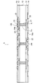
予備的事項に係る半導体装置の製造方法では、図1(a)に示すように、まず、上面に接続パッドPを備えた配線基板100を用意する。
In the method of manufacturing a semiconductor device according to the preliminary matter, as shown in FIG. 1A, first, a
次いで、図1(b)に示すように、配線基板100の上に先封止用の未硬化の封止樹脂材200aを形成する。さらに、図2に示すように、第1半導体チップ300を用意する。
Next, as shown in FIG. 1B, an uncured
第1半導体チップ300は素子形成面側にバンプ電極320を備え、背面側に接続電極340を備えている。半導体チップ300のバンプ電極320と接続電極340とは、不図示の貫通電極を介して接続されている。
The
そして、図2に図3(a)を加えて参照すると、第1半導体チップ300のバンプ電極320を封止樹脂材200aに押し込み、配線基板100の接続パッドPに圧接させる。
Then, referring to FIG. 3A with reference to FIG. 3A, the
さらに、加熱処理することにより、第1半導体チップ300のバンプ電極320の先端のはんだ(不図示)をリフローさせて、第1半導体チップ300のバンプ電極320を配線基板100の接続パッドPにフリップチップ接続する。
Further, the solder (not shown) at the tip of the
これにより、第1半導体チップ300と配線基板100との間に封止樹脂材200aから形成されるアンダーフィル樹脂200が充填される。アンダーフィル樹脂200は、第1半導体チップ300の側面を被覆して形成される。
Thereby, the
さらに、図3(b)に示すように、第1半導体チップ300の上に封止樹脂材220aを形成する。続いて、図4に示すように、素子形成面側にバンプ電極420を備えた第2半導体チップ400を用意する。第2半導体チップ400の面積は、第1半導体チップ300の面積よりも一回り大きく設定されている。
Further, as illustrated in FIG. 3B, a sealing
そして、図4に図5を加えて参照すると、第2半導体チップ400のバンプ電極420を封止樹脂材220aに押し込み、第1半導体チップ300の接続電極340に圧接させる。
Then, referring to FIG. 4 in addition to FIG. 5, the
さらに、加熱処理することにより、第2半導体チップ400のバンプ電極420の先端のはんだ(不図示)をリフローさせて、第2半導体チップ400のバンプ電極420を第1半導体チップ300の接続電極340にフリップチップ接続する。
Furthermore, the solder (not shown) at the tip of the
これにより、第2半導体チップ400と第1半導体チップ300との間、及び第2半導体チップ400と配線基板100との間に、封止樹脂材220aから形成されるアンダーフィル樹脂220が充填される。
Thus, the
このとき、図5に示すように、第2半導体チップ400の面積は第1半導体チップ300の面積よりも大きく設定されている。このため、第1半導体チップ300上の封止樹脂材220aは第2半導体チップ400の側面まで流動できずに、第2半導体チップ400の下面に留まった状態となる。
At this time, as shown in FIG. 5, the area of the
従って、第2半導体チップ400の側面の全体が大気に露出した状態となる。また、第2半導体チップ400の素子形成面の外周部も露出した状態となる。このため、図5の構造の半導体装置では、第2半導体チップ400の素子形成領域の側面から内部に水分が侵入し、特性劣化及び故障などを引き起こしやすくなり、信頼性を確保できなくなる。
Accordingly, the entire side surface of the
以下に説明する実施形態の半導体装置では、上側の第2半導体チップの面積が下側の第1半導体チップの面積よりも大きい場合であっても、第2半導体チップの側面をアンダーフィル樹脂で確実に被覆して信頼性を確保することができる。 In the semiconductor device of the embodiment described below, even if the area of the upper second semiconductor chip is larger than the area of the lower first semiconductor chip, the side surface of the second semiconductor chip is surely made of the underfill resin. It is possible to ensure the reliability by coating.
(実施形態)
図6〜図18は実施形態の半導体装置の製造方法を示す図、図19及び図20は実施形態の半導体装置を示す図である。以下、半導体装置の製造方法を説明しながら、半導体装置の構造について説明する。
(Embodiment)
6 to 18 are views showing a method of manufacturing the semiconductor device of the embodiment, and FIGS. 19 and 20 are views showing the semiconductor device of the embodiment. Hereinafter, the structure of the semiconductor device will be described while explaining the method for manufacturing the semiconductor device.
実施形態の半導体装置の製造方法では、まず、図6に示すような配線基板5を用意する。配線基板5は、厚み方向の中央部にコア基板10を備えている。コア基板10はガラスエポキシ樹脂などの絶縁材料から形成される。
In the semiconductor device manufacturing method of the embodiment, first, a
コア基板10の両面側に銅又は銅合金からなる第1配線層20がそれぞれ形成されている。コア基板10には厚み方向に貫通するスルーホールTHが形成されている。スルーホールTHの内壁にはスルーホールめっき層21が形成されており、スルーホールTHの残りの孔には樹脂体Rが充填されている。あるいは、コア基板10のスルーホールTHの全体に貫通電極が充填された構造を採用してもよい。
First wiring layers 20 made of copper or a copper alloy are formed on both sides of the
コア基板10の両面側の第1配線層20はスルーホールめっき層21を介して相互接続されている。コア基板10の両面側には、第1配線層20の接続部上にビアホールVHが配置された層間絶縁層12がそれぞれ形成されている。層間絶縁層12は、エポキシ樹脂又はポリイミド樹脂などの絶縁性樹脂から形成される。
The first wiring layers 20 on both sides of the
また、両面側の層間絶縁層12の上には、ビアホールVHを介して第1配線層20に接続される第2配線層22がそれぞれ形成されている。第2配線層22は銅又は銅合金から形成される。
Further, a
さらに、両面側の層間絶縁層12の上には、第2配線層22の接続部上に開口部14aが配置されたソルダレジスト層14がそれぞれ形成されている。ソルダレジスト層14は、ポリイミド樹脂又はアクリル樹脂などの絶縁性樹脂から形成される。
Further, a solder resist
そして、コア基板10の上面側の第2配線層22の接続部に、ニッケル/金めっき層、又ははんだ層などの接続電極CEが形成されている。
A connection electrode CE such as a nickel / gold plating layer or a solder layer is formed at the connection portion of the
そして、配線基板5に対して、温度:125℃程度で加熱処理することにより、水分を飛ばして乾燥させる。さらに、アルゴンプラズマで配線基板5の上面を処理することにより、濡れ性を向上させる。これにより、先封止用の封止樹脂材を形成するための前処理が完了する。
Then, the
次いで、図7に示すように、配線基板5の上に先封止用の第1封止樹脂材30aを形成する。第1封止樹脂材30aの好適な一例としては、最低溶融粘度が300Pa・sのエポキシ系樹脂、又は最低溶融粘度が20Pa・s〜90Pa・sのアクリル系樹脂が使用される。
Next, as shown in FIG. 7, a first
配線基板5には複数のチップ搭載領域が画定されており、図7では1つのチップ搭載領域が示されている。配線基板5の上に第1封止樹脂材30aを形成する具体例としては、まず、図8(a)に示すように、配線基板5の各チップ搭載領域の上に開口部24aが設けられたマスキングテープ24を貼付する。
A plurality of chip mounting areas are defined on the
図8(b)の平面図に示すように、マスキングテープ24の開口部24aは、四角形の各辺の中央が外側に延びた八角形の形状で形成される。
As shown in the plan view of FIG. 8B, the
次いで、図8(c)に示すように、マスキングテープ24が貼付された配線基板5の上に未硬化の樹脂シート30xを押圧して貼り付ける。さらに、図8(d)に示すように、マスキングテープ24を配線基板5から引き剥がす。
Next, as shown in FIG. 8C, an
これにより、マスキングテープ24の上に配置された部分の樹脂シート30xがマスキングテープ24と同時に除去される。その結果、マスキングテープ24の複数の開口部24aに配置された部分の樹脂シート30xが第1封止樹脂材30aとして配線基板5の上に残される。
As a result, the
このようにして、配線基板5の複数のチップ搭載領域に樹脂シート30xがそれぞれ分離されて配置され、第1封止樹脂材30aが島状に並んで形成される。第1封止樹脂材30aは、マスキングテープ24の開口部24aの形状に対応して八角形の形状で形成される。第1封止樹脂材30aを八角形の形状で形成する理由は、後述する第2封止樹脂材の変形に対応させるためである。
In this way, the
なお、樹脂シート30xを貼付する代わりに、ディスペンサなどによって液状樹脂を配線基板5の複数のチップ搭載領域に塗布してもよい。液状樹脂を使用する場合は、マスキングテープ24を必ずしも貼付する必要はない。
Instead of attaching the
続いて、図9に示すように、第1半導体チップ6を用意する。第1半導体チップ6は、例えば、シリコン基板を使用するCPUチップである。
Subsequently, as shown in FIG. 9, a
第1半導体チップ6では、シリコンからなるチップ基板40にその厚み方向に貫通するスルーホールTHが形成されている。また、スルーホールTHの内面及びチップ基板40の上面及び下面に絶縁層41が形成されている。
In the
絶縁層41としては、シリコン酸化層(SiO2層)、シリコン窒化層(SiN層)及びポリイミド層などから選択される。そして、スルーホールTH内に銅又は銅合金からなる貫通電極42が充填されている。
The insulating
貫通電極42の上端にはニッケル/金めっき層、又ははんだ層などの接続電極CExが形成されている。
A connection electrode CEx such as a nickel / gold plating layer or a solder layer is formed on the upper end of the through
また、チップ基板40の下面には貫通電極42の下端に接続される配線層44が形成されている。配線層44は、アルミニウム又は銅、あるいは、それらの合金から形成される。さらに、チップ基板40の下面に配線層44の接続部上に開口部45aが設けられたパッシベーション膜45が形成されている。
A
パッシベーション膜45は、シリコン酸化層、シリコン窒化層、又はポリイミド樹脂などから形成される。
The
配線層44の接続部には柱状電極PEが立設しており、柱状電極PEの先端に丸まったバンプ状のはんだ層46が形成されている。柱状電極PEは、例えば、銅又は銅合金からなる。また、第1半導体チップ6の柱状電極PEの配列ピッチは、例えば80μm〜100μmである。
A columnar electrode PE is erected at the connection portion of the
このようにして、第1半導体チップ6の下面側の柱状電極PEが配線層44、貫通電極42を介して上面側の接続電極CExに電気的に接続されて、上下面側が導通可能な構造となっている。
In this way, the columnar electrode PE on the lower surface side of the
第1半導体チップ6の下面側が素子形成面となっており、素子形成面には、不図示のトランジスタ、キャパシタ及び抵抗などの各種の素子が形成されており、それらが多層配線に接続されて電子回路が作り込まれている。
The lower surface side of the
そして、第1半導体チップ6内の電子回路が配線層44を介して柱状電極PEに接続されている。
The electronic circuit in the
前述した図7の第1封止樹脂材30aの面積は、第1半導体チップ6の面積より大きく設定されている。例えば、第1封止樹脂材30aの面積は9mm×9mm程度であり、第1半導体チップ6の面積は6mm×6mm程度である。
The area of the first
次いで、図10に示すように、図7の第1封止樹脂材30aが形成された配線基板5をボンディングステージ(不図示)の上に配置し、配線基板5を100℃程度に加熱して第1封止樹脂材30aを軟化させた状態とする。
Next, as shown in FIG. 10, the
そして、前述した図9の第1半導体チップ6の背面をボンディングツール16に吸着固定させる。ボンディングツール16の面積は、第1半導体チップ6の面積より大きく設定されており、配線基板5上の第1封止樹脂材30aの面積とほぼ同一である。このため、ボンディングツール16の周縁部16aが第1半導体チップ6の側面から外側にはみ出して露出した状態となる。
Then, the back surface of the
続いて、ボンディングツール16に吸着固定した第1半導体チップ6の柱状電極PEを配線基板5上の第1封止樹脂材30aに押し込む。これにより、図11に示すように、第1半導体チップ6の柱状電極PEをはんだ層46を介して配線基板5の接続電極CEに圧接させてフリップチップ実装する。
Subsequently, the columnar electrode PE of the
続いて、リフロー加熱することにより、はんだ層46を溶融させて第1半導体チップ6の柱状電極PEを配線基板5の接続電極CEにはんだ層46によって接合する。
Subsequently, the
さらに、第1封止樹脂材30aがエポキシ樹脂からなる場合は、温度:180℃、処理時間:1時間の条件で加熱処理して第1封止樹脂材30aを硬化させる。これにより、第1半導体チップ6と配線基板5との間に第1アンダーフィル樹脂30が充填される。
Furthermore, when the 1st sealing
このとき、第1半導体チップ6の外側に配置された第1封止樹脂材30aがボンディングツール16の周縁部16aによって押圧されて成型される。その後に、ボンディングツール16を第1半導体チップ6から取り外す。
At this time, the first
これにより、図12に示すように、第1半導体チップ6を取り囲む周囲の領域に、第1半導体チップ6と配線基板5との間の第1アンダーフィル樹脂30が延在して形成された環状の台座部31が形成される。そして、第1アンダーフィル樹脂30の台座部31の上面は第1半導体チップ6の上面と同一面となる。
As a result, as shown in FIG. 12, the
このようにして、第1アンダーフィル樹脂30のフィレット部分に多くの樹脂が配置されるようにし、フィレット部分を成型することにより、第1半導体チップ6の周囲に第1アンダーフィル樹脂30の台座部31を配置する。
In this way, a large amount of resin is arranged in the fillet portion of the
台座部31を含む第1アンダーフィル樹脂30の面積は、12mm×12mm程度である。
The area of the
次いで、図13に示すように、図12の構造体の第1半導体チップ6の上に第2封止樹脂材32aを形成する。第2封止樹脂材32aは、前述した第1封止樹脂材30aの形成方法と同様な方法で形成される。
Next, as shown in FIG. 13, a second
第2封止樹脂材32aの好適な一例としては、最低溶融粘度が10Pa・s〜90Pa・s、好適には30Pa・s〜50Pa・sのエポキシ系樹脂、又は最低溶融粘度が20Pa・s〜90Pa・sのアクリル系樹脂が使用される。
As a suitable example of the second
このように、第2封止樹脂32aとしては、最低溶融粘度の数値が二桁のものが好ましく、エポキシ系樹脂を使用する場合は、前述した第1封止樹脂材30aよりも最低溶融粘度が低い樹脂材が使用される。
As described above, the
第2封止樹脂材32aとして溶融粘度の低い樹脂を使用する理由は、以下の通りである。後述するように第2半導体チップの狭ピッチの柱状電極を低い荷重で第2封止樹脂32aに押し込んでフリップチップ接続する際に、接続部分への樹脂やフィラーの噛み込みの発生を防止するためである。
The reason why a resin having a low melt viscosity is used as the second
次いで、図14に示すように、第1半導体チップ6の上に積層される第2半導体チップ7を用意する。第2半導体チップ7は、例えば、シリコン基板を使用するメモリチップである。第2半導体チップ7の面積は第1半導体チップ6の面積より大きく設定されている。前述した図13の第2封止樹脂材32aの面積は、第2半導体チップ7の面積に対応するように設定される。
Next, as shown in FIG. 14, a
また、第2半導体チップ7の面積は台座部31を含む第1アンダーフィル樹脂30の面積よりも小さく設定されている。
The area of the
第2半導体チップ7では、シリコンからなるチップ基板50の下面側の素子形成面に接続パッドPが形成されている。第2半導体チップ7は、第1半導体チップ6と同様に素子形成面に電子回路が作り込まれており、接続パッドPが電子回路に接続されている。
In the
また、素子形成面側に最外層として、接続パッドPの上に開口部52aが配置されたパッシベーション膜52が形成されている。パッシベーション膜52は、シリコン酸化層、シリコン窒化層、又はポリイミド樹脂などから形成される。
Further, a
さらに、接続パッドPにはパッシベーション膜52から外側に立設する柱状電極PExが接続されており、柱状電極PExの先端にはんだ層54が形成されている。柱状電極PExは、例えば、銅又は銅合金から形成される。
Further, a columnar electrode PEx standing outward from the
第2半導体チップ7の柱状電極PExの配列ピッチは例えば40μm程度であり、第1半導体チップ6の柱状電極PEよりも狭ピッチ化されている。
The arrangement pitch of the columnar electrodes PEx of the
そして、図15に示すように、図14の第2半導体チップ7の背面をボンディングツール16に吸着固定させる。続いて、ボンディングツール16に吸着固定した第2半導体チップ7の柱状電極PExを第1半導体チップ6上の第2封止樹脂材32aに押し込む。
Then, as shown in FIG. 15, the back surface of the
これにより、図16に示すように、第2半導体チップ7の柱状電極PExをはんだ層54を介して第1半導体チップ6の接続電極CExに圧接させてフリップチップ実装する。
As a result, as shown in FIG. 16, the columnar electrode PEx of the
続いて、リフロー加熱することにより、はんだ層54を溶融させて第2半導体チップ7の柱状電極PExを第1半導体チップ6の接続電極CExにはんだ層54によって接合する。
Subsequently, the
その後に、第2封止樹脂材32aがエポキシ樹脂からなる場合は、温度:165℃、処理時間:2時間の条件で加熱処理して,第2封止樹脂材32aを硬化させる。これにより、第2半導体チップ7と、第1半導体チップ6及び第1アンダーフィル樹脂30との間に第2アンダーフィル樹脂32が充填される。
Then, when the 2nd sealing
このとき、第2半導体チップ7を第2封止樹脂材32aに押し込む際に、第2封止樹脂材32aは第1アンダーフィル樹脂30の台座部31の上に流動しながら第2半導体チップ7の側面を被覆する。
At this time, when the
これにより、第2半導体チップ7の面積が第1半導体チップ6の面積よりも大きい場合であっても、第2半導体チップ7の側面を第2アンダーフィル樹脂32で確実に封止することができる。
Thereby, even if the area of the
前述したように、第2半導体チップ7の柱状電極PExの配列ピッチは、第1半導体チップ6の柱状電極PEと比較してかなり狭く設定され、第1半導体チップ6との間隔も狭くなる。
As described above, the arrangement pitch of the columnar electrodes PEx of the
しかも、第2半導体チップ7をフリップチップ接続する際に、第1半導体チップ6へのダメージを低減させるため、第2半導体チップ7に印加する荷重を低くする必要がある。
In addition, when the
このため、第2封止樹脂材32aの溶融粘度が高い場合は、第1半導体チップ6の接続電極CExと第2半導体チップ7の柱状電極PExとの間に樹脂やフィラーの噛み込みが発生する懸念がある。
For this reason, when the melt viscosity of the second
そこで、本願発明者は、第2封止樹脂材32aとして、最低溶融粘度が100Pa・s以上(300Pa.s)のエポキシ樹脂材と、最低溶融粘度が100Pa・s未満(50Pa・s)のエポキシ樹脂材とを振り分けて実験を行った。そして、両者の樹脂材において、第1半導体チップ6の接続電極CExと第2半導体チップ7の柱状電極PExとの接合の様子をSEM(走査電子顕微鏡)にて観察した。
Therefore, the inventor of the present application uses, as the second
その結果によれば、最低溶融粘度が100Pa・s以上(300Pa.s)の粘度が高いエポキシ樹脂材では、第2半導体チップ7の柱状電極PExの先端のはんだ層54と第1半導体チップ6の接続電極CExとの間に樹脂やフィラーが残る噛み込みが発生しており、電気接続の信頼性が得られないことが分かった。
According to the result, in the case of an epoxy resin material having a minimum melt viscosity of 100 Pa · s or higher (300 Pa · s), the
これに対して、最低溶融粘度が100Pa・s未満(50Pa・s)の粘度が低いエポキシ樹脂材では、第2半導体チップ7の柱状電極PExの先端のはんだ層54と第1半導体チップ6の接続電極CExとの間に樹脂は確認されず、良好な接合が得られることが確認された。
On the other hand, in the case of an epoxy resin material having a minimum melt viscosity of less than 100 Pa · s (50 Pa · s), the
このように、狭ピッチの柱状電極PExを備えた第2半導体チップ7を先封止技術で第1半導体チップ6に低い荷重でフリップチップ接続する際には、溶融粘度の低い樹脂材を使用することが有効であることが確認された。
Thus, when the flip-chip bonding at a narrow pitch low load the second
また、第2半導体チップ7は比較的面積が大きいことから、平面視して四角状の第2封止樹脂材32aに第2半導体チップ7を押し込む際に、第2封止樹脂材32aの4つの角部よりも各辺の中央が外側に延びて、より顕著な八角状の形状になりやすい。
Further, since the
このため、前述した図8で説明したように、第1封止樹脂材30aは、第2封止樹脂材32aの変形に対応できるように、平面視して八角形の形状で形成される。
Therefore, as described with reference to FIG. 8 described above, the first
これにより、第2アンダーフィル樹脂32が第1アンダーフィル樹脂30の側面に流れて形成されることが防止される。第1アンダーフィル樹脂30の側面に第2アンダーフィル樹脂32が流れて形成されると膜剥がれなどが発生して信頼性が低下するため、第1アンダーフィル樹脂30の側面に第2アンダーフィル樹脂32が流れ込まないようにする。
This prevents the
その後に、図17に示すように、第2半導体チップ7からボンディングツール16を取り外す。
Thereafter, as shown in FIG. 17, the
あるいは、図18に示すように、前述したような先封止技術を使用しないで、第1半導体チップ6の接続電極CExに第2半導体チップ7の柱状電極PExをフリップチップ接続した後に、それらの隙間に第2アンダーフィル樹脂32を充填してもよい。
Alternatively, as shown in FIG. 18, without using the above-described pre-sealing technique, the columnar electrodes PEx of the
この場合は、第1アンダーフィル樹脂30の台座部31の上にディスペンサ18から樹脂を塗布できるので、図17と同様に第2半導体チップ7の側面を第2アンダーフィル樹脂32で確実に封止することができる。
In this case, since the resin can be applied from the
次いで、図19に示すように、配線基板5及び第2半導体チップ7の上にモールド樹脂34を形成して、第1、第2アンダーフィル樹脂30、32の側面から第2半導体チップ7の上面までを樹脂封止する。
Next, as shown in FIG. 19, a
なお、第1、第2アンダーフィル樹脂30、32によって第1、第2半導体チップ6,7が十分に保護される場合は、モールド樹脂34を省略してもよい。
If the first and
さらに、配線基板5の下面側の第2配線層22の接続部にはんだボールを搭載するなどして外部接続端子Tを形成する。その後に、第1半導体チップ6及び第2半導体チップ7が積層された各チップ搭載領域が得られるように、配線基板5を切断する。
Further, the external connection terminals T are formed by mounting solder balls on the connection portions of the
以上により、実施形態の半導体装置1が製造される。 As described above, the semiconductor device 1 of the embodiment is manufactured.
図19に示すように、実施形態の半導体装置1では、前述した図6の配線基板5の上面側の接続電極CEに前述した図9の第1半導体チップ6の柱状電極PEがはんだ層46を介してフリップチップ接続されている。
As shown in FIG. 19, in the semiconductor device 1 of the embodiment, the columnar electrode PE of the
第1半導体チップ6と配線基板5との間には第1アンダーフィル樹脂30が充填されている。第1アンダーフィル樹脂30は、第1半導体チップ6と配線基板5との間の領域から第1半導体チップ6の周囲の領域に延在する環状の台座部31を備えて形成されている。
A
さらに、第1半導体チップ6の上面側の接続電極CExには、前述した図14の第2半導体チップ7の柱状電極PExがはんだ層54を介してフリップチップ接続されている。また、第1半導体チップ6と第2半導体チップ7との間に第2アンダーフィル樹脂32が充填されている。
Further, the columnar electrode PEx of the
第2アンダーフィル樹脂32は、第1半導体チップ6と第2半導体チップ7との間の領域から第1アンダーフィル樹脂30の台座部31の上に延在し、第2半導体チップ7の側面を封止している。
The
第2半導体チップ7の下面側の素子形成領域の側面が少なくとも第2アンダーフィル樹脂32で封止されていればよく、第2半導体チップ7の背面側に近い側面は露出していてもよい。
The side surface of the element formation region on the lower surface side of the
第2半導体チップ7の面積は第1半導体チップ6の面積よりも大きく設定されている。しかし、第1半導体チップ6の周囲に第1アンダーフィル樹脂30の台座部31が配置され、第2半導体チップ7の側面は、第1半導体チップ6の側面と第1アンダーフィル樹脂30の台座部31の側面との間の領域に配置されている。
The area of the
このため、台座部31上に配置された第2封止樹脂材32aから形成される第2アンダーフィル樹脂32によって第2半導体チップ7の側面を確実に封止することができる。
For this reason, the side surface of the
あるいは、第1アンダーフィル樹脂30の台座部31をさらに外側に延ばし、第2封止樹脂材32aを厚くすることにより、第2半導体チップ7の側面の全体を第2アンダーフィル樹脂32で封止することも可能である。
Alternatively, the
このように、本実施形態の半導体装置1は、第1半導体チップ6の周囲に第1アンダーフィル樹脂30の台座部31を配置している。このため、第1半導体チップ6の上にそれより面積が大きな第2半導体チップ7がフリップチップ接続されるとしても、第1アンダーフィル樹脂30の台座部31の上に第2アンダーフィル樹脂32を配置することができる。
Thus, in the semiconductor device 1 of the present embodiment, the
これにより、第1半導体チップ6の側面より外側に配置される第2半導体チップ7の側面を第2アンダーフィル樹脂32で封止することが可能になる。
As a result, the side surface of the
その結果、第2半導体チップ7の素子形成領域の側面を第2アンダーフィル樹脂32で確実に封止することができる。よって、第2半導体チップ7の電子回路への水分の侵入が阻止され、特性劣化及び故障などの不具合の発生が防止される。
As a result, the side surface of the element formation region of the
図20には、実施形態の変形例の半導体装置1aが示されている。図20の変形例の半導体装置1aでは、前述した図17の第2半導体チップ7の背面(上面)が露出するようにモールド樹脂34が第1、第2アンダーフィル樹脂30,32及び第2半導体チップ7の周囲に形成されている。
FIG. 20 shows a
さらに、第2半導体チップ7の上面及びモールド樹脂34の上面に接着層36を介して放熱部材60が接着されている。接着層36として、TIM(Thermal Interface Material)と呼ばれるような熱伝導性に優れた樹脂による接着剤が使用される。
Further, a
これにより、第2半導体チップ7の背面に放熱部材60が接続されて、放熱性に優れた半導体装置となる。放熱部材60としては、銅などからなるヒートスプレッダ、放熱フィンを備えたヒートシンク、又はヒートパイプなどを使用することができる。
Thereby, the
(その他の形態)
前述した実施形態では、配線基板5の上に第1半導体チップ6及び第2半導体チップ7を順にフリップチップ接続して積層している。この形態の他に、配線基板5の代わりに、半導体チップを採用し、3つの半導体チップを積層して同様な構成としてもよい。
(Other forms)
In the above-described embodiment, the
あるいは、第1半導体チップ6の代わりに、シリコンインターポーザなどの他の配線基板を採用し、配線基板の上に他の配線基板及び半導体チップを積層して同様な構成としてもよい。
Alternatively, instead of the
さらには、第1半導体チップ6及び第2半導体チップ7の代わりに、各種の配線基板を採用し、3つの配線基板を積層して同様な構成としてもよい。
Furthermore, instead of the
1,1a…半導体装置、5…配線基板、6…第1半導体チップ、7…第2半導体チップ、10…コア基板、12…層間絶縁層、14…ソルダレジスト層、14a,24a,45a…開口部、16…ボンディングツール、16a…周縁部、20…第1配線層、21…スルーホールめっき層、22…第2配線層、24…マスキングテープ、30…第1アンダーフィル樹脂、31…台座部、30a…第1封止樹脂材、30x…樹脂シート、32…第2アンダーフィル樹脂、32a…第2封止樹脂材、34…モールド樹脂、36…接着層、40,50…チップ基板、41…絶縁層、42…貫通電極、44…配線層、45,52…パッシベーション膜、46,54…はんだ層、60…放熱部材、CE,CEx…接続電極、P…接続パッド、PE,PEx…柱状電極、R…樹脂体,TH…スルーホール、VH…ビアホール。
DESCRIPTION OF
Claims (11)
前記配線基板の上に電極を介してフリップチップ接続された第1半導体チップと、
前記配線基板と前記第1半導体チップの間に充填された充填部と、前記第1半導体チップの周囲に配置された台座部とを備え、前記充填部と前記台座部とが一体的に繋がって形成された一層構造からなる第1アンダーフィル樹脂と、
前記第1半導体チップの上にフリップチップ接続され、前記第1半導体チップより面積が大きな第2半導体チップと、
前記第1半導体チップと前記第2半導体チップの間に充填され、かつ前記第1アンダーフィル樹脂の台座部の上面及び前記第2半導体チップの側面を被覆する第2アンダーフィル樹脂と
を有し、
前記第1半導体チップの上面と前記第1アンダーフィル樹脂の台座部の上面とは、同一面となっており、
前記第1アンダーフィル樹脂の周囲の前記配線基板の上面が前記第1アンダーフィル樹脂から露出しており、かつ、
前記第2アンダーフィル樹脂の側面の上端が前記第2半導体チップの側面に接しており、前記第2半導体チップの側面の上部、及び上面が前記第2アンダーフィル樹脂から露出していることを特徴とする半導体装置。 A wiring board;
A first semiconductor chip flip-chip connected to the wiring board via an electrode ;
A filling portion filled in between the said circuit board first semiconductor chip, e Bei a base portion disposed around the first semiconductor chip, and the filling portion and the base portion is connected integrally A first underfill resin having a single layer structure formed by
A second semiconductor chip flip-chip connected on the first semiconductor chip and having a larger area than the first semiconductor chip;
Filled between said first semiconductor chip second semiconductor chip, and have a second underfill resin for covering the upper surface and a side surface of the second semiconductor chip of the base portion of the first underfill resin,
The upper surface of the first semiconductor chip and the upper surface of the base portion of the first underfill resin are the same surface,
An upper surface of the wiring substrate around the first underfill resin is exposed from the first underfill resin; and
The upper end of the side surface of the second underfill resin is in contact with the side surface of the second semiconductor chip, and the upper and upper surfaces of the side surface of the second semiconductor chip are exposed from the second underfill resin. A semiconductor device.
前記第1封止樹脂材に第1半導体チップの電極を押し込んで前記配線基板にフリップチップ接続することにより、前記配線基板と前記第1半導体チップとの間に充填された充填部と、前記第1半導体チップの周囲に配置された台座部とを備え、前記充填部と前記台座部とが一体的に繋がって形成された一層構造からなる第1アンダーフィル樹脂を形成する工程と、
前記第1半導体チップの上に第2封止樹脂材を形成する工程と、
前記第2封止樹脂材に第2半導体チップの電極を押し込んで前記第1半導体チップにフリップチップ接続し、前記第1半導体チップと前記第2半導体チップとの間に第2アンダーフィル樹脂を充填すると共に、前記第1アンダーフィル樹脂の台座部の上面及び第2半導体チップの側面を前記第2アンダーフィル樹脂で被覆する工程と
を有し、
前記第1半導体チップの上面と前記第1アンダーフィル樹脂の台座部の上面とが同一面となって形成され、
前記第1アンダーフィル樹脂の周囲の前記配線基板の上面が前記第1アンダーフィル樹脂から露出し、
前記第2アンダーフィル樹脂の側面の上端が前記第2半導体チップの側面に接し、前記第2半導体チップの側面の上部、及び上面が前記第2アンダーフィル樹脂から露出することを特徴とする半導体装置の製造方法。 Forming a first sealing resin material on the wiring board;
A filling portion filled between the wiring substrate and the first semiconductor chip by pressing an electrode of the first semiconductor chip into the first sealing resin material and flip-chip connection to the wiring substrate; A step of forming a first underfill resin having a single layer structure formed by integrally connecting the filling portion and the pedestal portion, and a pedestal portion disposed around one semiconductor chip;
Forming a second sealing resin material on the first semiconductor chip;
An electrode of a second semiconductor chip is pushed into the second sealing resin material to be flip-chip connected to the first semiconductor chip, and a second underfill resin is filled between the first semiconductor chip and the second semiconductor chip. And covering the upper surface of the base portion of the first underfill resin and the side surface of the second semiconductor chip with the second underfill resin,
The upper surface of the first semiconductor chip and the upper surface of the pedestal portion of the first underfill resin are formed in the same plane,
An upper surface of the wiring board around the first underfill resin is exposed from the first underfill resin;
An upper end of a side surface of the second underfill resin is in contact with a side surface of the second semiconductor chip, and an upper portion and an upper surface of the side surface of the second semiconductor chip are exposed from the second underfill resin. Manufacturing method.
前記封止樹脂材に第1半導体チップの電極を押し込んで前記配線基板にフリップチップ接続することにより、前記配線基板と前記第1半導体チップとの間に充填された充填部と、前記第1半導体チップの周囲に配置された台座部とを備え、前記充填部と前記台座部とが一体的に繋がって形成された一層構造からなる第1アンダーフィル樹脂を形成する工程と、
前記第1半導体チップの上に第2半導体チップをフリップチップ接続する工程と、
前記第1半導体チップと前記第2半導体チップとの間に第2アンダーフィル樹脂を充填すると共に、前記第1アンダーフィル樹脂の台座部の上面及び第2半導体チップの側面を前記第2アンダーフィル樹脂で被覆する工程と
を有し、
前記第1半導体チップの上面と前記第1アンダーフィル樹脂の台座部の上面とが同一面となって形成され、
前記第1アンダーフィル樹脂の周囲の前記配線基板の上面が前記第1アンダーフィル樹脂から露出し、
前記第2アンダーフィル樹脂の側面の上端が前記第2半導体チップの側面に接し、前記第2半導体チップの側面の上部、及び上面が前記第2アンダーフィル樹脂から露出することを特徴とする半導体装置の製造方法。 Forming a sealing resin material on the wiring board;
A filling portion filled between the wiring substrate and the first semiconductor chip by pressing an electrode of the first semiconductor chip into the sealing resin material and making a flip chip connection to the wiring substrate; and the first semiconductor A step of forming a first underfill resin having a single layer structure formed by integrally connecting the filling portion and the pedestal portion, and a pedestal portion disposed around the chip;
Flip chip connecting a second semiconductor chip on the first semiconductor chip;
The second underfill resin is filled between the first semiconductor chip and the second semiconductor chip, and the upper surface of the base portion of the first underfill resin and the side surface of the second semiconductor chip are disposed on the second underfill resin. in possess a step of coating,
The upper surface of the first semiconductor chip and the upper surface of the pedestal portion of the first underfill resin are formed in the same plane,
An upper surface of the wiring board around the first underfill resin is exposed from the first underfill resin;
An upper end of a side surface of the second underfill resin is in contact with a side surface of the second semiconductor chip, and an upper portion and an upper surface of the side surface of the second semiconductor chip are exposed from the second underfill resin. Manufacturing method.
前記第1半導体チップは、前記第1半導体チップよりも面積が大きなボンディングツールに固定された状態で前記第1封止樹脂材に押し込まれ、
前記ボンディングツールの周縁部の下面で前記第1封止樹脂材の周縁部が押圧されて前記台座部が形成され、前記台座部の上面と前記第1半導体チップの上面とが同一面となることを特徴とする請求項5又は6に記載の半導体装置の製造方法。 In the step of filling the first underfill resin,
The first semiconductor chip is pressed into the first sealing resin material in a state of being fixed to a bonding tool having a larger area than the first semiconductor chip,
The periphery of the first sealing resin material is pressed on the lower surface of the periphery of the bonding tool to form the pedestal, and the upper surface of the pedestal and the upper surface of the first semiconductor chip are flush with each other. A method of manufacturing a semiconductor device according to claim 5 or 6 .
前記第1アンダーフィル樹脂から露出している前記配線基板の上面、前記第1アンダーフィル樹脂の側面、前記第2アンダーフィル樹脂の側面、及び前記第2半導体チップを被覆するモールド樹脂を形成する工程を有することを特徴とする請求項5乃至9のいずれか一項に記載の半導体装置の製造方法。Forming an upper surface of the wiring board exposed from the first underfill resin, a side surface of the first underfill resin, a side surface of the second underfill resin, and a mold resin that covers the second semiconductor chip; 10. The method of manufacturing a semiconductor device according to claim 5, comprising:
Priority Applications (2)
| Application Number | Priority Date | Filing Date | Title |
|---|---|---|---|
| JP2014024242A JP6242231B2 (en) | 2014-02-12 | 2014-02-12 | Semiconductor device and manufacturing method thereof |
| US14/567,056 US9633978B2 (en) | 2014-02-12 | 2014-12-11 | Semiconductor device and method of manufacturing the same |
Applications Claiming Priority (1)
| Application Number | Priority Date | Filing Date | Title |
|---|---|---|---|
| JP2014024242A JP6242231B2 (en) | 2014-02-12 | 2014-02-12 | Semiconductor device and manufacturing method thereof |
Publications (3)
| Publication Number | Publication Date |
|---|---|
| JP2015153811A JP2015153811A (en) | 2015-08-24 |
| JP2015153811A5 JP2015153811A5 (en) | 2016-11-24 |
| JP6242231B2 true JP6242231B2 (en) | 2017-12-06 |
Family
ID=53775605
Family Applications (1)
| Application Number | Title | Priority Date | Filing Date |
|---|---|---|---|
| JP2014024242A Active JP6242231B2 (en) | 2014-02-12 | 2014-02-12 | Semiconductor device and manufacturing method thereof |
Country Status (2)
| Country | Link |
|---|---|
| US (1) | US9633978B2 (en) |
| JP (1) | JP6242231B2 (en) |
Families Citing this family (8)
| Publication number | Priority date | Publication date | Assignee | Title |
|---|---|---|---|---|
| TWI566305B (en) * | 2014-10-29 | 2017-01-11 | 巨擘科技股份有限公司 | Method for manufacturing three-dimensional integrated circuit |
| KR102356810B1 (en) * | 2015-01-22 | 2022-01-28 | 삼성전기주식회사 | Printed circuit board having embedded electronic devices and method of manufacturing the same |
| JP6489965B2 (en) * | 2015-07-14 | 2019-03-27 | 新光電気工業株式会社 | Electronic component device and manufacturing method thereof |
| JP6478853B2 (en) * | 2015-07-14 | 2019-03-06 | 新光電気工業株式会社 | Electronic component device and manufacturing method thereof |
| US10957672B2 (en) * | 2017-11-13 | 2021-03-23 | Taiwan Semiconductor Manufacturing Company, Ltd. | Package structure and method of manufacturing the same |
| US11075133B2 (en) * | 2018-06-29 | 2021-07-27 | Taiwan Semiconductor Manufacturing Company, Ltd. | Underfill structure for semiconductor packages and methods of forming the same |
| JP2020047793A (en) * | 2018-09-19 | 2020-03-26 | 株式会社東芝 | Manufacturing method of semiconductor device |
| JP2022002261A (en) * | 2020-06-22 | 2022-01-06 | キオクシア株式会社 | Storage device |
Family Cites Families (10)
| Publication number | Priority date | Publication date | Assignee | Title |
|---|---|---|---|---|
| JP2002184936A (en) * | 2000-12-11 | 2002-06-28 | Matsushita Electric Ind Co Ltd | Semiconductor device and its manufacturing method |
| JP3683179B2 (en) * | 2000-12-26 | 2005-08-17 | 松下電器産業株式会社 | Semiconductor device and manufacturing method thereof |
| JP2003258034A (en) * | 2002-03-06 | 2003-09-12 | Mitsubishi Electric Corp | Method for manufacturing multilayer wiring base and multilayer wiring base |
| JP2011054851A (en) * | 2009-09-03 | 2011-03-17 | Toshiba Corp | Method for manufacturing semiconductor device |
| JP2011061004A (en) * | 2009-09-10 | 2011-03-24 | Elpida Memory Inc | Semiconductor device, and method of manufacturing the same |
| KR101719636B1 (en) * | 2011-01-28 | 2017-04-05 | 삼성전자 주식회사 | Semiconductor device and fabricating method thereof |
| JP5357241B2 (en) | 2011-08-10 | 2013-12-04 | 新光電気工業株式会社 | Semiconductor device and manufacturing method of semiconductor device |
| JP2013115190A (en) * | 2011-11-28 | 2013-06-10 | Elpida Memory Inc | Semiconductor device manufacturing method |
| JP2013138177A (en) * | 2011-11-28 | 2013-07-11 | Elpida Memory Inc | Semiconductor device manufacturing method |
| JP2015122445A (en) * | 2013-12-24 | 2015-07-02 | ルネサスエレクトロニクス株式会社 | Semiconductor device and manufacturing method of the same |
-
2014
- 2014-02-12 JP JP2014024242A patent/JP6242231B2/en active Active
- 2014-12-11 US US14/567,056 patent/US9633978B2/en active Active
Also Published As
| Publication number | Publication date |
|---|---|
| JP2015153811A (en) | 2015-08-24 |
| US9633978B2 (en) | 2017-04-25 |
| US20150228624A1 (en) | 2015-08-13 |
Similar Documents
| Publication | Publication Date | Title |
|---|---|---|
| JP6242231B2 (en) | Semiconductor device and manufacturing method thereof | |
| JP5579402B2 (en) | Semiconductor device, method for manufacturing the same, and electronic device | |
| TWI628750B (en) | Power overlay structure and method of making same | |
| TWI508255B (en) | Thermally dissipating flip-chip package | |
| US20140295620A1 (en) | Method of manufacturing semiconductor device having plural semiconductor chips stacked one another | |
| US9698072B2 (en) | Low-stress dual underfill packaging | |
| US9691676B2 (en) | Semiconductor device and method for manufacturing the same | |
| JP5893387B2 (en) | Electronic device and manufacturing method thereof | |
| US9338886B2 (en) | Substrate for mounting semiconductor, semiconductor device and method for manufacturing semiconductor device | |
| US9583367B2 (en) | Methods and apparatus for bump-on-trace chip packaging | |
| TW201448137A (en) | Power overlay structure and method of making same | |
| JP6478853B2 (en) | Electronic component device and manufacturing method thereof | |
| JP6489965B2 (en) | Electronic component device and manufacturing method thereof | |
| US20110049707A1 (en) | Semiconductor device and method of manufacturing the semiconductor device | |
| US20120146242A1 (en) | Semiconductor device and method of fabricating the same | |
| TW201448139A (en) | Embedded substrate package and the method of making the same | |
| JP2013021058A (en) | Manufacturing method of semiconductor device | |
| JP2016039290A (en) | Printed wiring board and semiconductor package | |
| US20130277828A1 (en) | Methods and Apparatus for bump-on-trace Chip Packaging | |
| TWI688067B (en) | Semiconductor device and its manufacturing method | |
| TW200933831A (en) | Integrated circuit package and the method for fabricating thereof | |
| TWI576979B (en) | Package substrate and method for manufacturing the same | |
| JP2008198916A (en) | Semiconductor device and manufacturing method thereof | |
| TWI450348B (en) | Electronic device with vertical conductive connectors and method thereof | |
| TWI591788B (en) | Method for manufacturing electronic package |
Legal Events
| Date | Code | Title | Description |
|---|---|---|---|
| A521 | Request for written amendment filed |
Free format text: JAPANESE INTERMEDIATE CODE: A523 Effective date: 20161004 |
|
| A621 | Written request for application examination |
Free format text: JAPANESE INTERMEDIATE CODE: A621 Effective date: 20161004 |
|
| A977 | Report on retrieval |
Free format text: JAPANESE INTERMEDIATE CODE: A971007 Effective date: 20170612 |
|
| A131 | Notification of reasons for refusal |
Free format text: JAPANESE INTERMEDIATE CODE: A131 Effective date: 20170725 |
|
| A521 | Request for written amendment filed |
Free format text: JAPANESE INTERMEDIATE CODE: A523 Effective date: 20170906 |
|
| TRDD | Decision of grant or rejection written | ||
| A01 | Written decision to grant a patent or to grant a registration (utility model) |
Free format text: JAPANESE INTERMEDIATE CODE: A01 Effective date: 20171031 |
|
| A61 | First payment of annual fees (during grant procedure) |
Free format text: JAPANESE INTERMEDIATE CODE: A61 Effective date: 20171107 |
|
| R150 | Certificate of patent or registration of utility model |
Ref document number: 6242231 Country of ref document: JP Free format text: JAPANESE INTERMEDIATE CODE: R150 |