JP6235981B2 - Method for processing an object - Google Patents
Method for processing an object Download PDFInfo
- Publication number
- JP6235981B2 JP6235981B2 JP2014219285A JP2014219285A JP6235981B2 JP 6235981 B2 JP6235981 B2 JP 6235981B2 JP 2014219285 A JP2014219285 A JP 2014219285A JP 2014219285 A JP2014219285 A JP 2014219285A JP 6235981 B2 JP6235981 B2 JP 6235981B2
- Authority
- JP
- Japan
- Prior art keywords
- gas
- region
- plasma
- fluorocarbon
- etching
- Prior art date
- Legal status (The legal status is an assumption and is not a legal conclusion. Google has not performed a legal analysis and makes no representation as to the accuracy of the status listed.)
- Active
Links
- 238000012545 processing Methods 0.000 title claims description 151
- 238000000034 method Methods 0.000 title claims description 130
- 239000007789 gas Substances 0.000 claims description 294
- 230000008569 process Effects 0.000 claims description 73
- 230000001681 protective effect Effects 0.000 claims description 54
- NBVXSUQYWXRMNV-UHFFFAOYSA-N fluoromethane Chemical compound FC NBVXSUQYWXRMNV-UHFFFAOYSA-N 0.000 claims description 53
- 238000005530 etching Methods 0.000 claims description 49
- 150000004767 nitrides Chemical class 0.000 claims description 28
- VYPSYNLAJGMNEJ-UHFFFAOYSA-N Silicium dioxide Chemical compound O=[Si]=O VYPSYNLAJGMNEJ-UHFFFAOYSA-N 0.000 claims description 23
- 229910052814 silicon oxide Inorganic materials 0.000 claims description 19
- 229910052581 Si3N4 Inorganic materials 0.000 claims description 16
- HQVNEWCFYHHQES-UHFFFAOYSA-N silicon nitride Chemical compound N12[Si]34N5[Si]62N3[Si]51N64 HQVNEWCFYHHQES-UHFFFAOYSA-N 0.000 claims description 16
- XUIMIQQOPSSXEZ-UHFFFAOYSA-N Silicon Chemical compound [Si] XUIMIQQOPSSXEZ-UHFFFAOYSA-N 0.000 claims description 12
- 229910052710 silicon Inorganic materials 0.000 claims description 12
- 239000010703 silicon Substances 0.000 claims description 12
- 150000002500 ions Chemical class 0.000 claims description 11
- 238000004380 ashing Methods 0.000 claims description 5
- 238000010438 heat treatment Methods 0.000 claims description 5
- 238000009832 plasma treatment Methods 0.000 claims description 5
- UFHFLCQGNIYNRP-UHFFFAOYSA-N Hydrogen Chemical compound [H][H] UFHFLCQGNIYNRP-UHFFFAOYSA-N 0.000 claims description 4
- 239000001257 hydrogen Substances 0.000 claims description 4
- 229910052739 hydrogen Inorganic materials 0.000 claims description 4
- 239000000126 substance Substances 0.000 claims description 3
- 102000035118 modified proteins Human genes 0.000 claims description 2
- 108091005573 modified proteins Proteins 0.000 claims description 2
- 230000003647 oxidation Effects 0.000 claims 1
- 238000007254 oxidation reaction Methods 0.000 claims 1
- LIVNPJMFVYWSIS-UHFFFAOYSA-N silicon monoxide Chemical group [Si-]#[O+] LIVNPJMFVYWSIS-UHFFFAOYSA-N 0.000 claims 1
- 239000010410 layer Substances 0.000 description 25
- 239000011737 fluorine Substances 0.000 description 19
- 229910052731 fluorine Inorganic materials 0.000 description 19
- YCKRFDGAMUMZLT-UHFFFAOYSA-N Fluorine atom Chemical compound [F] YCKRFDGAMUMZLT-UHFFFAOYSA-N 0.000 description 17
- 230000000052 comparative effect Effects 0.000 description 13
- 239000003507 refrigerant Substances 0.000 description 11
- 238000007790 scraping Methods 0.000 description 10
- 229940070337 ammonium silicofluoride Drugs 0.000 description 8
- IJGRMHOSHXDMSA-UHFFFAOYSA-N Atomic nitrogen Chemical compound N#N IJGRMHOSHXDMSA-UHFFFAOYSA-N 0.000 description 7
- DDFHBQSCUXNBSA-UHFFFAOYSA-N 5-(5-carboxythiophen-2-yl)thiophene-2-carboxylic acid Chemical compound S1C(C(=O)O)=CC=C1C1=CC=C(C(O)=O)S1 DDFHBQSCUXNBSA-UHFFFAOYSA-N 0.000 description 6
- MYMOFIZGZYHOMD-UHFFFAOYSA-N Dioxygen Chemical compound O=O MYMOFIZGZYHOMD-UHFFFAOYSA-N 0.000 description 6
- 125000004429 atom Chemical group 0.000 description 6
- 230000015572 biosynthetic process Effects 0.000 description 6
- 229910001882 dioxygen Inorganic materials 0.000 description 6
- 229910052782 aluminium Inorganic materials 0.000 description 5
- XAGFODPZIPBFFR-UHFFFAOYSA-N aluminium Chemical compound [Al] XAGFODPZIPBFFR-UHFFFAOYSA-N 0.000 description 5
- 230000005669 field effect Effects 0.000 description 5
- 239000000463 material Substances 0.000 description 4
- 229910021420 polycrystalline silicon Inorganic materials 0.000 description 4
- 238000005299 abrasion Methods 0.000 description 3
- 230000007423 decrease Effects 0.000 description 3
- 230000008021 deposition Effects 0.000 description 3
- 238000009792 diffusion process Methods 0.000 description 3
- 238000010494 dissociation reaction Methods 0.000 description 3
- 230000005593 dissociations Effects 0.000 description 3
- -1 fluorine ions Chemical class 0.000 description 3
- 239000011261 inert gas Substances 0.000 description 3
- 229910052757 nitrogen Inorganic materials 0.000 description 3
- 239000000919 ceramic Substances 0.000 description 2
- 239000011248 coating agent Substances 0.000 description 2
- 238000000576 coating method Methods 0.000 description 2
- 238000004519 manufacturing process Methods 0.000 description 2
- 238000005259 measurement Methods 0.000 description 2
- 230000007246 mechanism Effects 0.000 description 2
- 238000001020 plasma etching Methods 0.000 description 2
- 239000000758 substrate Substances 0.000 description 2
- 238000012546 transfer Methods 0.000 description 2
- QGZKDVFQNNGYKY-UHFFFAOYSA-O Ammonium Chemical compound [NH4+] QGZKDVFQNNGYKY-UHFFFAOYSA-O 0.000 description 1
- OKTJSMMVPCPJKN-UHFFFAOYSA-N Carbon Chemical compound [C] OKTJSMMVPCPJKN-UHFFFAOYSA-N 0.000 description 1
- 229910003902 SiCl 4 Inorganic materials 0.000 description 1
- 230000004075 alteration Effects 0.000 description 1
- QVGXLLKOCUKJST-UHFFFAOYSA-N atomic oxygen Chemical compound [O] QVGXLLKOCUKJST-UHFFFAOYSA-N 0.000 description 1
- 230000036760 body temperature Effects 0.000 description 1
- 239000006227 byproduct Substances 0.000 description 1
- 229910052799 carbon Inorganic materials 0.000 description 1
- 239000004020 conductor Substances 0.000 description 1
- 239000002826 coolant Substances 0.000 description 1
- 238000001816 cooling Methods 0.000 description 1
- 238000005520 cutting process Methods 0.000 description 1
- 230000003247 decreasing effect Effects 0.000 description 1
- 238000010586 diagram Methods 0.000 description 1
- 229910001873 dinitrogen Inorganic materials 0.000 description 1
- 230000009477 glass transition Effects 0.000 description 1
- 150000002431 hydrogen Chemical class 0.000 description 1
- 239000011810 insulating material Substances 0.000 description 1
- 239000011229 interlayer Substances 0.000 description 1
- 230000001678 irradiating effect Effects 0.000 description 1
- 229910052751 metal Inorganic materials 0.000 description 1
- 239000002184 metal Substances 0.000 description 1
- 238000012986 modification Methods 0.000 description 1
- 230000004048 modification Effects 0.000 description 1
- 238000005121 nitriding Methods 0.000 description 1
- 239000001301 oxygen Substances 0.000 description 1
- 229910052760 oxygen Inorganic materials 0.000 description 1
- 230000002093 peripheral effect Effects 0.000 description 1
- 238000000206 photolithography Methods 0.000 description 1
- 239000000047 product Substances 0.000 description 1
- 239000010453 quartz Substances 0.000 description 1
- 238000003860 storage Methods 0.000 description 1
- 239000002344 surface layer Substances 0.000 description 1
- XLYOFNOQVPJJNP-UHFFFAOYSA-N water Substances O XLYOFNOQVPJJNP-UHFFFAOYSA-N 0.000 description 1
Images


Classifications
-
- H—ELECTRICITY
- H01—ELECTRIC ELEMENTS
- H01L—SEMICONDUCTOR DEVICES NOT COVERED BY CLASS H10
- H01L21/00—Processes or apparatus adapted for the manufacture or treatment of semiconductor or solid state devices or of parts thereof
- H01L21/70—Manufacture or treatment of devices consisting of a plurality of solid state components formed in or on a common substrate or of parts thereof; Manufacture of integrated circuit devices or of parts thereof
- H01L21/71—Manufacture of specific parts of devices defined in group H01L21/70
- H01L21/768—Applying interconnections to be used for carrying current between separate components within a device comprising conductors and dielectrics
- H01L21/76897—Formation of self-aligned vias or contact plugs, i.e. involving a lithographically uncritical step
-
- H—ELECTRICITY
- H01—ELECTRIC ELEMENTS
- H01L—SEMICONDUCTOR DEVICES NOT COVERED BY CLASS H10
- H01L29/00—Semiconductor devices adapted for rectifying, amplifying, oscillating or switching, or capacitors or resistors with at least one potential-jump barrier or surface barrier, e.g. PN junction depletion layer or carrier concentration layer; Details of semiconductor bodies or of electrodes thereof ; Multistep manufacturing processes therefor
- H01L29/66—Types of semiconductor device ; Multistep manufacturing processes therefor
- H01L29/66007—Multistep manufacturing processes
- H01L29/66075—Multistep manufacturing processes of devices having semiconductor bodies comprising group 14 or group 13/15 materials
- H01L29/66227—Multistep manufacturing processes of devices having semiconductor bodies comprising group 14 or group 13/15 materials the devices being controllable only by the electric current supplied or the electric potential applied, to an electrode which does not carry the current to be rectified, amplified or switched, e.g. three-terminal devices
- H01L29/66409—Unipolar field-effect transistors
- H01L29/66477—Unipolar field-effect transistors with an insulated gate, i.e. MISFET
- H01L29/66787—Unipolar field-effect transistors with an insulated gate, i.e. MISFET with a gate at the side of the channel
- H01L29/66795—Unipolar field-effect transistors with an insulated gate, i.e. MISFET with a gate at the side of the channel with a horizontal current flow in a vertical sidewall of a semiconductor body, e.g. FinFET, MuGFET
-
- H—ELECTRICITY
- H01—ELECTRIC ELEMENTS
- H01L—SEMICONDUCTOR DEVICES NOT COVERED BY CLASS H10
- H01L21/00—Processes or apparatus adapted for the manufacture or treatment of semiconductor or solid state devices or of parts thereof
- H01L21/02—Manufacture or treatment of semiconductor devices or of parts thereof
- H01L21/04—Manufacture or treatment of semiconductor devices or of parts thereof the devices having at least one potential-jump barrier or surface barrier, e.g. PN junction, depletion layer or carrier concentration layer
- H01L21/18—Manufacture or treatment of semiconductor devices or of parts thereof the devices having at least one potential-jump barrier or surface barrier, e.g. PN junction, depletion layer or carrier concentration layer the devices having semiconductor bodies comprising elements of Group IV of the Periodic System or AIIIBV compounds with or without impurities, e.g. doping materials
- H01L21/30—Treatment of semiconductor bodies using processes or apparatus not provided for in groups H01L21/20 - H01L21/26
- H01L21/31—Treatment of semiconductor bodies using processes or apparatus not provided for in groups H01L21/20 - H01L21/26 to form insulating layers thereon, e.g. for masking or by using photolithographic techniques; After treatment of these layers; Selection of materials for these layers
- H01L21/3105—After-treatment
- H01L21/311—Etching the insulating layers by chemical or physical means
- H01L21/31105—Etching inorganic layers
- H01L21/31111—Etching inorganic layers by chemical means
- H01L21/31116—Etching inorganic layers by chemical means by dry-etching
-
- H—ELECTRICITY
- H01—ELECTRIC ELEMENTS
- H01L—SEMICONDUCTOR DEVICES NOT COVERED BY CLASS H10
- H01L21/00—Processes or apparatus adapted for the manufacture or treatment of semiconductor or solid state devices or of parts thereof
- H01L21/70—Manufacture or treatment of devices consisting of a plurality of solid state components formed in or on a common substrate or of parts thereof; Manufacture of integrated circuit devices or of parts thereof
- H01L21/71—Manufacture of specific parts of devices defined in group H01L21/70
- H01L21/768—Applying interconnections to be used for carrying current between separate components within a device comprising conductors and dielectrics
- H01L21/76801—Applying interconnections to be used for carrying current between separate components within a device comprising conductors and dielectrics characterised by the formation and the after-treatment of the dielectrics, e.g. smoothing
- H01L21/76802—Applying interconnections to be used for carrying current between separate components within a device comprising conductors and dielectrics characterised by the formation and the after-treatment of the dielectrics, e.g. smoothing by forming openings in dielectrics
- H01L21/76814—Applying interconnections to be used for carrying current between separate components within a device comprising conductors and dielectrics characterised by the formation and the after-treatment of the dielectrics, e.g. smoothing by forming openings in dielectrics post-treatment or after-treatment, e.g. cleaning or removal of oxides on underlying conductors
-
- H—ELECTRICITY
- H01—ELECTRIC ELEMENTS
- H01L—SEMICONDUCTOR DEVICES NOT COVERED BY CLASS H10
- H01L29/00—Semiconductor devices adapted for rectifying, amplifying, oscillating or switching, or capacitors or resistors with at least one potential-jump barrier or surface barrier, e.g. PN junction depletion layer or carrier concentration layer; Details of semiconductor bodies or of electrodes thereof ; Multistep manufacturing processes therefor
- H01L29/40—Electrodes ; Multistep manufacturing processes therefor
- H01L29/401—Multistep manufacturing processes
-
- H—ELECTRICITY
- H01—ELECTRIC ELEMENTS
- H01L—SEMICONDUCTOR DEVICES NOT COVERED BY CLASS H10
- H01L2221/00—Processes or apparatus adapted for the manufacture or treatment of semiconductor or solid state devices or of parts thereof covered by H01L21/00
- H01L2221/10—Applying interconnections to be used for carrying current between separate components within a device
- H01L2221/1005—Formation and after-treatment of dielectrics
- H01L2221/1052—Formation of thin functional dielectric layers
- H01L2221/1057—Formation of thin functional dielectric layers in via holes or trenches
- H01L2221/1063—Sacrificial or temporary thin dielectric films in openings in a dielectric
Description
本発明の実施形態は、被処理体を処理する方法に関するものである。 Embodiments described herein relate generally to a method for processing an object to be processed.
フィン型の電界効果トランジスタといった素子を有する電子デバイスの製造においては、コンタクト形成のために、SAC(Self−Aligned Contact)加工が用いられている。 In the manufacture of electronic devices having elements such as fin-type field effect transistors, SAC (Self-Aligned Contact) processing is used for contact formation.
SAC加工の対象となる被処理体は、下地層、二つの隆起領域、窒化領域、及び酸化領域を有している。下地層は、例えば多結晶シリコン層である。二つの隆起領域は、例えば、ゲートであり、多結晶シリコンから構成されている。これら隆起領域は互いに離間して下地層上に設けられている。窒化領域は、窒化シリコン製であり、二つの隆起領域及び下地層を覆うように設けられている。酸化領域は、酸化シリコン製であり、窒化領域を覆うように設けられている。 A target object to be subjected to SAC processing has a base layer, two raised regions, a nitrided region, and an oxidized region. The underlayer is, for example, a polycrystalline silicon layer. The two raised regions are, for example, gates and are made of polycrystalline silicon. These raised areas are spaced apart from each other and are provided on the underlying layer. The nitride region is made of silicon nitride and is provided so as to cover the two raised regions and the base layer. The oxidized region is made of silicon oxide and is provided so as to cover the nitrided region.
SAC加工では、酸化領域の表面から二つの隆起領域の間の領域を通って下地層まで達するホールが酸化領域に形成される。一般的に、SAC加工では、このような開口を形成するために、フルオロカーボンガスのプラズマを用いて、酸化領域がエッチングされ、下地層に接する窒化領域がエッチングされる。なお、このようなSAC加工については、特許文献1に記載されている。 In the SAC processing, holes reaching the base layer from the surface of the oxidized region through the region between the two raised regions are formed in the oxidized region. In general, in the SAC processing, in order to form such an opening, the oxidized region is etched and the nitrided region in contact with the base layer is etched using plasma of fluorocarbon gas. Such SAC processing is described in Patent Document 1.
フルオロカーボンガスのプラズマによる酸化領域のエッチングでは、ホールの底、特に、窒化領域の隅部に、酸化シリコンからなる残渣が発生する。したがって、形成されるホールの底の幅は狭くなる。このような形状のホールを更に深く加工するために、窒化領域をエッチングしようとしても、当該窒化領域のエッチングを十分に行うことができない。また、フルオロカーボンガスのプラズマ中の活性種、例えば、フッ素の活性種によって隆起領域を覆う窒化領域、特に、窒化領域の角部が削られてしまう。 In the etching of the oxidized region by the plasma of fluorocarbon gas, a residue made of silicon oxide is generated at the bottom of the hole, particularly at the corner of the nitrided region. Therefore, the width of the bottom of the hole to be formed becomes narrow. Even if an attempt is made to etch a nitride region in order to process a hole having such a shape deeper, the nitride region cannot be etched sufficiently. In addition, the nitrided region that covers the raised region by the active species in the plasma of the fluorocarbon gas, for example, the fluorine active species, in particular, the corners of the nitrided region are scraped.
したがって、SACでは、隆起領域を覆う窒化領域の削れを低減しつつ、ホールといった開口内の残渣及び下地層直上の窒化領域をエッチングすることが必要である。 Therefore, in the SAC, it is necessary to etch the residue in the opening such as a hole and the nitride region immediately above the base layer while reducing the abrasion of the nitride region covering the raised region.
一側面においては、被処理体を処理する方法が提供される。被処理体は、下地層、該下地層上に互いに離間して設けられた二つの隆起領域、二つの隆起領域を覆う第1部分及び下地層を覆う第2部分を含む窒化シリコン製の窒化領域、及び、窒化領域を覆う酸化シリコン製の酸化領域を有する。本方法は、被処理体を処理して、酸化領域から二つの隆起領域の間を通って下地層まで達する開口を形成するものである。この方法は、(1)二つの隆起領域の間で第2部分を露出させる開口を酸化領域に形成する工程(以下、「第1工程」という)と、(2)開口内の酸化シリコン製の残渣及び第2部分をエッチングする工程(以下、「第2工程」という)であり、水素を含有するガス及びNF3ガスを含む混合ガスのプラズマに被処理体を晒して残渣及び第2部分を変質させることにより変質領域を形成し、該変質領域を除去する、該工程と、を含む。 In one aspect, a method for processing a workpiece is provided. The object to be treated includes a nitride layer made of silicon nitride, including a base layer, two raised regions provided on the base layer so as to be spaced apart from each other, a first part covering the two raised regions, and a second part covering the base layer And an oxide region made of silicon oxide covering the nitride region. In this method, an object to be processed is processed to form an opening extending from the oxidized region to the underlying layer through the two raised regions. This method includes (1) a step of forming an opening exposing the second portion between two raised regions in the oxidized region (hereinafter referred to as “first step”), and (2) a silicon oxide made in the opening. Etching the residue and the second portion (hereinafter referred to as “second step”), exposing the object to be processed to plasma of a mixed gas containing a gas containing hydrogen and NF 3 gas to remove the residue and the second portion. Forming an altered region by altering and removing the altered region.
この方法では、残渣を化学的にケイフッ化アンモニウムに変質させて変質領域を形成し、当該変質領域を除去する。したがって、ホールの底の残渣を除去することが可能である。また、窒化シリコン製の第2部分をも、ケイフッ化アンモニウムに変質させて除去することができる。さらに、従来のフルオロカーボンガスのプラズマでは残渣を除去できないために第2部分を除去するまでに、隆起領域を覆う窒化領域、即ち第1部分、特に当該第1部分の肩部が大きく削られてしまうが、本方法によれば、残渣が除去されるので、第2部分の除去中の第1部分の削れを低減させることが可能である。 In this method, the residue is chemically altered to ammonium silicofluoride to form an altered region, and the altered region is removed. Therefore, it is possible to remove the residue at the bottom of the hole. Further, the second portion made of silicon nitride can also be removed by being transformed into ammonium silicofluoride. Further, since the residue cannot be removed by the conventional plasma of fluorocarbon gas, the nitrided region covering the raised region, that is, the first portion, particularly the shoulder portion of the first portion, is greatly shaved before the second portion is removed. However, according to this method, since the residue is removed, it is possible to reduce the abrasion of the first part during the removal of the second part.
一実施形態では、第2工程に用いられる混合ガスは、H2ガス及びNF3ガスを含んでいてもよい。この混合ガスによれば、残渣及び第2部分を一括して除去することが可能である。 In one embodiment, the mixed gas used in the second step may include H 2 gas and NF 3 gas. According to this mixed gas, it is possible to remove the residue and the second portion all at once.
一実施形態では、第2工程は、(2a)NH3ガス及びNF3ガスを含む混合ガスのプラズマに被処理体を晒して変質領域を形成し、該変質領域を除去する工程と、(2b)H2ガス及びNF3ガスを含む混合ガスのプラズマに被処理体を晒して変質領域を形成し、該変質領域を除去する工程と、を含む。 In one embodiment, the second step includes (2a) exposing the target object to plasma of a mixed gas containing NH 3 gas and NF 3 gas to form an altered region, and removing the altered region (2b) ) in the plasma of a mixed gas containing H 2 gas and NF 3 gas by exposing the object to be processed to form a modified region, and a step of removing the modified protein region.
酸化シリコンをケイフッ化アンモニウムに変質させるためには、混合ガスからフッ化アンモニウムを生成する必要がある。混合ガスがNH3ガス及びNF3ガスを含む場合には、低解離のプラズマを発生させることによってフッ化アンモニウムを生成することができる。したがって、窒化シリコンの削れの原因となるフッ素及びHFの活性種の発生量を低減させることができ、窒化シリコンに対して酸化シリコンを比較的高い選択性でエッチングすることができる。一方、混合ガスがH2ガス及びNF3ガスを含む混合ガスを用いる場合には、高解離のプラズマを発生させることによってフッ化アンモニウムを生成することができる。H2ガス及びNF3ガスを含む混合ガスを用いる場合には、高解離のプラズマ中で比較的多量のフッ素及びHFの活性種が生成される。したがって、窒化シリコンのエッチング対する酸化シリコンのエッチング選択性は低くなるが、窒化シリコンのエッチングレートを高めることができる。 In order to transform silicon oxide into ammonium silicofluoride, it is necessary to produce ammonium fluoride from the mixed gas. When the mixed gas contains NH 3 gas and NF 3 gas, ammonium fluoride can be generated by generating low dissociation plasma. Therefore, it is possible to reduce the generation amount of active species of fluorine and HF that cause silicon nitride to be scraped, and it is possible to etch silicon oxide with relatively high selectivity with respect to silicon nitride. On the other hand, when a mixed gas containing H 2 gas and NF 3 gas is used as the mixed gas, ammonium fluoride can be generated by generating highly dissociated plasma. When a mixed gas containing H 2 gas and NF 3 gas is used, a relatively large amount of active species of fluorine and HF are generated in a highly dissociated plasma. Accordingly, the etching selectivity of silicon oxide with respect to the etching of silicon nitride is lowered, but the etching rate of silicon nitride can be increased.
上記実施形態では、残渣及び第2部分の除去の初期段階、特に残渣の除去時に、NH3ガス及びNF3ガスを含む混合ガスを用いることにより、残渣の除去が行われている期間中の第1部分の削れを抑制することができる。次いで、H 2 ガス及びNF3ガスを含む混合ガスを用いることにより、第2部分のエッチングレートを高めることができる。したがって、第1部分の削れを更に低減しつつ、残渣及び第2部分を除去することが可能となる。 In the above embodiment, by using a mixed gas containing NH 3 gas and NF 3 gas at the initial stage of removal of the residue and the second portion, particularly at the time of removal of the residue, the first removal during the period during which the residue is being removed is performed. Scraping of one part can be suppressed. Next, the etching rate of the second portion can be increased by using a mixed gas containing H 2 gas and NF 3 gas. Therefore, it is possible to remove the residue and the second portion while further reducing the wear of the first portion.
一実施形態では、被処理体を加熱することによって変質領域が除去されてもよい。或いは、一実施形態では、容量結合型のプラズマ処理装置のシリコン製の上部電極に正イオンを引きつけることによって該上部電極から放出される二次電子に被処理体を晒すことによって、変質領域が除去されてもよい。 In one embodiment, the altered region may be removed by heating the workpiece. Alternatively, in one embodiment, the altered region is removed by exposing the workpiece to secondary electrons emitted from the upper electrode by attracting positive ions to the silicon upper electrode of the capacitively coupled plasma processing apparatus. May be.
一実施形態では、第1工程は、(1a)窒化領域上及び酸化領域上に保護膜を形成する工程(以下、「第3工程」という)であり、被処理体をフルオロカーボンガスのプラズマに晒して、酸化領域上に形成される保護膜よりも厚い保護膜を窒化領域上に形成する、該工程と、(1b)酸化領域をエッチングする工程(以下、第4工程」という)であり、フルオロカーボンガスのプラズマに被処理体を晒す、該工程と、を含む。この実施形態では、第3工程において被処理体を載置する載置台に供給される高周波バイアス電力が、第4工程において載置台に供給される高周波バイアス電力よりも小さく、第3工程において被処理体の温度が60℃以上250℃以下の温度に設定される。一実施形態では、第3工程及び第4工程は、交互に繰り返されてもよい。また、一実施形態では、第3工程において高周波バイアス電力が載置台に供給されなくてもよい。また、一実施形態では、第3工程において、フルオロカーボンガスとして、C4F6、C4F8、及びC6F6のうち少なくとも一種を含むガスが用いられてもよい。 In one embodiment, the first step is (1a) a step of forming a protective film on the nitrided region and the oxidized region (hereinafter referred to as “third step”), and the object to be processed is exposed to fluorocarbon gas plasma. Forming a protective film thicker than the protective film formed on the oxidized region on the nitrided region, and (1b) etching the oxidized region (hereinafter referred to as a fourth step), Exposing the object to be processed to a plasma of gas. In this embodiment, the high frequency bias power supplied to the mounting table on which the object to be processed is mounted in the third step is smaller than the high frequency bias power supplied to the mounting table in the fourth step, and the processing target is processed in the third step. The body temperature is set to a temperature of 60 ° C. or higher and 250 ° C. or lower. In one embodiment, the third step and the fourth step may be alternately repeated. In one embodiment, the high frequency bias power may not be supplied to the mounting table in the third step. In one embodiment, in the third step, a gas containing at least one of C 4 F 6 , C 4 F 8 , and C 6 F 6 may be used as the fluorocarbon gas.
60℃以上250℃以下の温度環境下では、窒化領域上に形成されるフルオロカーボンの保護膜の厚さは、酸化領域上に形成される当該保護膜の厚さよりも大きくなる。また、比較的低いバイアス電力が供給された状態では、窒化領域のエッチングレートは低くなる。したがって、上記実施形態によれば、第3工程において厚い保護膜を窒化領域上に形成することができ、第4工程において選択的に酸化領域をエッチングする際に窒化領域の削れを抑制することが可能となる。 Under a temperature environment of 60 ° C. or more and 250 ° C. or less, the thickness of the protective film of fluorocarbon formed on the nitrided region is larger than the thickness of the protective film formed on the oxidized region. In addition, the etching rate of the nitriding region is low when a relatively low bias power is supplied. Therefore, according to the above embodiment, a thick protective film can be formed on the nitrided region in the third step, and when the oxide region is selectively etched in the fourth step, the nitrided region can be prevented from being scraped. It becomes possible.
一実施形態では、第1工程は、(1c)被処理体をフルオロカーボンガスを含む処理ガスのプラズマに晒す工程(以下、「第5工程」という)であり、酸化領域をエッチングし、且つ、該酸化領域上にフルオロカーボンを含む堆積物を形成する、該工程と、(1d)堆積物に含まれるフルオロカーボンのラジカルにより酸化領域をエッチングする工程(以下、「第6工程」という)と、を含む。この実施形態では、第5工程と第6工程が、交互に繰り返される。 In one embodiment, the first step is (1c) a step of exposing the object to be processed to a plasma of a processing gas containing a fluorocarbon gas (hereinafter referred to as “fifth step”), etching the oxidized region, and Forming a deposit containing a fluorocarbon on the oxidized region; and (1d) etching the oxidized region with a radical of the fluorocarbon contained in the deposit (hereinafter referred to as “sixth step”). In this embodiment, the fifth step and the sixth step are alternately repeated.
この実施形態では、第5工程において生成されるフルオロカーボンガスのプラズマによって酸化領域がエッチングされ、当該酸化領域上に堆積物が形成される。次いで、第6工程において、堆積物に含まれるフルオロカーボンのラジカルを用いて酸化領域が更にエッチングされる。また、第6工程では、堆積物の量が減少する、したがって、再び第5工程を行うことにより、酸化領域のエッチングが更に進行する。かかる第5工程及び第6工程が交互に繰り返されることにより、酸化領域、即ちシリコン酸化膜のエッチングの停止を防止することが可能となる。その結果、酸化領域のエッチングを継続して行うことが可能となる。 In this embodiment, the oxidized region is etched by the fluorocarbon gas plasma generated in the fifth step, and a deposit is formed on the oxidized region. Next, in a sixth step, the oxidized region is further etched using the fluorocarbon radicals contained in the deposit. Further, in the sixth step, the amount of deposits is reduced. Therefore, the etching of the oxidized region further proceeds by performing the fifth step again. By alternately repeating the fifth step and the sixth step, it is possible to prevent the etching of the oxide region, that is, the silicon oxide film, from being stopped. As a result, it becomes possible to continue the etching of the oxidized region.
一実施形態では、第6工程では、希ガスのプラズマに被処理体が晒されてもよい。この実施形態では、希ガス原子のイオンが堆積物に衝突することにより、当該堆積物中のフルオロカーボンラジカルが酸化領域をエッチングする。なお、一実施形態の第6工程では、フルオロカーボンガスが実質的に供給されなくてもよい。 In one embodiment, in the sixth step, the object to be processed may be exposed to rare gas plasma. In this embodiment, the ions of rare gas atoms collide with the deposit, so that the fluorocarbon radical in the deposit etches the oxidized region. In the sixth step of one embodiment, the fluorocarbon gas may not be substantially supplied.
一実施形態の方法は、第1部分及び第2部分上に別の保護膜を形成する工程を更に含み、該別の保護膜を形成する工程は第1工程と第2工程との間に実行される。別の保護膜を形成する工程では、フルオロカーボンガスのプラズマ処理が実行されてもよい。即ち、別の保護膜は、フルオロカーボンを含む保護膜であってもよい。保護膜の形成に寄与する分子の量は、隆起領域の頂部近傍では多く、酸化領域に形成された開口の深部では少なくなる。したがって、保護膜の膜厚は、隆起領域の頂部近傍で大きくなり、開口の深部近傍では小さくなる。したがって、第1部分の削れを更に抑制しつつ、残渣及び第2部分をエッチングすることが可能となる。 The method of an embodiment further includes the step of forming another protective film on the first portion and the second portion, and the step of forming the additional protective film is performed between the first step and the second step. Is done. In the step of forming another protective film, a plasma treatment of fluorocarbon gas may be performed. That is, the other protective film may be a protective film containing fluorocarbon. The amount of molecules contributing to the formation of the protective film is large in the vicinity of the top of the raised region and is small in the deep portion of the opening formed in the oxidized region. Therefore, the thickness of the protective film increases near the top of the raised region and decreases near the deep portion of the opening. Therefore, it is possible to etch the residue and the second portion while further suppressing the scraping of the first portion.
一実施形態の方法は、前記開口が形成された被処理体上の有機物を除去するためのアッシング処理を実行する工程を更に含み得る。別の保護膜を形成する工程は、アッシング処理を実行する工程と第2工程との間に実行され得る。 The method of an embodiment may further include a step of performing an ashing process for removing organic substances on the object to be processed in which the opening is formed. The step of forming another protective film may be performed between the step of executing the ashing process and the second step.
以上説明したように、SAC加工において隆起領域を覆う窒化領域の削れを低減しつつ、ホールといった開口内の残渣及び下地層直上の窒化領域をエッチングすることが可能となる。 As described above, it is possible to etch the residue in the opening such as a hole and the nitride region immediately above the base layer while reducing the abrasion of the nitride region covering the raised region in the SAC process.
以下、図面を参照して種々の実施形態について詳細に説明する。なお、各図面において同一又は相当の部分に対しては同一の符号を附すこととする。 Hereinafter, various embodiments will be described in detail with reference to the drawings. In the drawings, the same or corresponding parts are denoted by the same reference numerals.
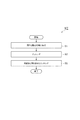
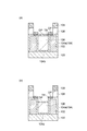
図1は、一実施形態に係る被処理体を処理する方法を示す流れ図である。図1に示す方法MTは、被処理体(以下、「ウエハW」という)に開口を形成する方法である。この方法MTは、一例においては、図2に示す被処理体にホールといった開口を形成するために利用することができる。 FIG. 1 is a flowchart illustrating a method for processing an object to be processed according to an embodiment. A method MT shown in FIG. 1 is a method of forming an opening in an object to be processed (hereinafter referred to as “wafer W”). In one example, the method MT can be used to form an opening such as a hole in the object to be processed shown in FIG.
図2は、被処理体の一例を示す断面図である。図2に示すウエハWは、下地層100、複数の隆起領域102、窒化領域104、酸化領域106、及び、マスク108を有している。このウエハWは、例えば、フィン型電界効果トランジスタの製造中に得られる生産物であり得る。
FIG. 2 is a cross-sectional view illustrating an example of an object to be processed. The wafer W shown in FIG. 2 has a
下地層100は、例えば、多結晶シリコンから構成され得る。下地層100は、一例においては、基板に設けられたフィン型電界効果トランジスタのフィン領域であり、一対の側面と当該一対の側面の上端の間で延在する上面とによって規定される形状を有する。一例では、下地層100は、略直方体形状を有し得る。
The
複数の隆起領域102は、下地層100よりも上方に隆起するように設けられた領域である。複数の隆起領域102は、下地層100上において互いに離間して設けられている。例えば、複数の隆起領域102は、互いに離間して略平行に配列されている。これら隆起領域102は、一例においては、フィン型電界効果トランジスタのゲート領域であり、多結晶シリコン製の領域であり得る。この一例においては、隆起領域102は、フィン領域である下地層100が延在する方向に直交する方向に延在しており、一対の側面と当該一対の側面の上端の間で延在する上面とによって規定される形状を有する。例えば、隆起領域102は、略直方体形状を有し得る。なお、隆起領域102の個数は2以上であれば、任意の個数であり得る。
The plurality of raised
窒化領域104は、窒化シリコンから構成されており、第1部分104a及び第2部分104bを含んでいる。第1部分104aは、隆起領域102を覆うように設けられている。第1部分104aは、隆起領域102の表面に接している。また、第2部分104bは、第1部分104aに連続しており、隣接する隆起領域102の間において下地層100上に設けられている。
The
酸化領域106は、酸化シリコンから構成されている。酸化領域106は、窒化領域104を覆うように設けられている。即ち、酸化領域106は、窒化領域104を覆うように隣接する隆起領域102の間に埋め込まれており、隆起領域102及び窒化領域104の上方に略平坦な面を提供している。この酸化領域106は、一例においてはフィン型電界効果トランジスタの層間絶縁層であり得る。
The oxidized
酸化領域106上には、マスク108が設けられている。マスク108は、隣接する隆起領域102間の上方において開口するパターンを有している。このマスク108は、有機膜から構成されている。なお、マスク108は、フォトリソグラフィによって作成することが可能である。
A
方法MTは、隣接する隆起領域102の間において酸化領域106の上面から下地層100の上面まで達する開口を形成するために利用される。即ち、隣接する隆起領域102の間に自己整合的に開口、例えば、ホールを形成するために利用される。以下、ウエハWに形成される開口がホールであるものとして説明を続ける。このホールは、一例においては、フィン領域のソース又はドレインに接続するコンタクト用のホールとなり得る。
The method MT is used to form an opening between adjacent raised
以下、方法MTの実施に利用可能なプラズマ処理装置について説明する。図3は、一実施形態に係るプラズマ処理装置を概略的に示す図である。図3に示すプラズマ処理装置10は、容量結合型プラズマエッチング装置であり、処理容器12を備えている。処理容器12は、略円筒形状を有している。処理容器12は、例えば、アルミニウムから構成されており、その内壁面には陽極酸化処理が施されている。この処理容器12は保安接地されている。
Hereinafter, a plasma processing apparatus that can be used to perform the method MT will be described. FIG. 3 is a diagram schematically illustrating a plasma processing apparatus according to an embodiment. A
処理容器12の底部上には、略円筒状の支持部14が設けられている。支持部14は、例えば、絶縁材料から構成されている。支持部14は、処理容器12内において、処理容器12の底部から鉛直方向に延在している。また、処理容器12内には、載置台PDが設けられている。載置台PDは、支持部14によって支持されている。
A substantially
載置台PDは、その上面においてウエハWを保持する。載置台PDは、下部電極LE及び静電チャックESCを有している。下部電極LEは、第1プレート18a及び第2プレート18bを含んでいる。第1プレート18a及び第2プレート18bは、例えばアルミニウムといった金属から構成されており、略円盤形状をなしている。第2プレート18bは、第1プレート18a上に設けられており、第1プレート18aに電気的に接続されている。
The mounting table PD holds the wafer W on the upper surface thereof. The mounting table PD includes a lower electrode LE and an electrostatic chuck ESC. The lower electrode LE includes a first plate 18a and a
第2プレート18b上には、静電チャックESCが設けられている。静電チャックESCは、導電膜である電極を一対の絶縁層又は絶縁シート間に配置した構造を有している。静電チャックESCの電極には、直流電源22がスイッチ23を介して電気的に接続されている。この静電チャックESCは、直流電源22からの直流電圧により生じたクーロン力等の静電力によりウエハWを吸着する。これにより、静電チャックESCは、ウエハWを保持することができる。
An electrostatic chuck ESC is provided on the
第2プレート18bの周縁部上には、ウエハWのエッジ及び静電チャックESCを囲むようにフォーカスリングFRが配置されている。フォーカスリングFRは、エッチングの均一性を向上させるために設けられている。フォーカスリングFRは、エッチング対象の膜の材料によって適宜選択される材料から構成されており、例えば、石英から構成され得る。
A focus ring FR is disposed on the peripheral edge of the
第2プレート18bの内部には、冷媒流路24が設けられている。冷媒流路24は、温調機構を構成している。冷媒流路24には、処理容器12の外部に設けられたチラーユニットから配管26aを介して冷媒が供給される。冷媒流路24に供給された冷媒は、配管26bを介してチラーユニットに戻される。このように、冷媒流路24には、冷媒が循環するよう、供給される。この冷媒の温度を制御することにより、静電チャックESCによって支持されたウエハWの温度が制御される。
A coolant channel 24 is provided inside the
また、プラズマ処理装置10には、ガス供給ライン28が設けられている。ガス供給ライン28は、伝熱ガス供給機構からの伝熱ガス、例えばHeガスを、静電チャックESCの上面とウエハWの裏面との間に供給する。
The
また、プラズマ処理装置10には、加熱素子であるヒータHTが設けられている。ヒータHTは、例えば、第2プレート18b内に埋め込まれている。ヒータHTには、ヒータ電源HPが接続されている。ヒータ電源HPからヒータHTに電力が供給されることにより、載置台PDの温度が調整され、当該載置台PD上に載置されるウエハWの温度が調整されるようになっている。なお、ヒータHTは、静電チャックESCに内蔵されていてもよい。
Further, the
また、プラズマ処理装置10は、上部電極30を備えている。上部電極30は、載置台PDの上方において、当該載置台PDと対向配置されている。下部電極LEと上部電極30とは、互いに略平行に設けられている。これら上部電極30と下部電極LEとの間には、ウエハWにプラズマ処理を行うための処理空間Sが提供されている。
In addition, the
上部電極30は、絶縁性遮蔽部材32を介して、処理容器12の上部に支持されている。一実施形態では、上部電極30は、載置台PDの上面、即ち、ウエハ載置面からの鉛直方向における距離が可変であるように構成され得る。上部電極30は、電極板34及び電極支持体36を含み得る。電極板34は処理空間Sに面しており、当該電極板34には複数のガス吐出孔34aが設けられている。この電極板34は、一実施形態では、シリコンから構成されている。
The
電極支持体36は、電極板34を着脱自在に支持するものであり、例えばアルミニウムといった導電性材料から構成され得る。この電極支持体36は、水冷構造を有し得る。電極支持体36の内部には、ガス拡散室36aが設けられている。このガス拡散室36aからは、ガス吐出孔34aに連通する複数のガス通流孔36bが下方に延びている。また、電極支持体36には、ガス拡散室36aに処理ガスを導くガス導入口36cが形成されており、このガス導入口36cには、ガス供給管38が接続されている。
The
ガス供給管38には、バルブ群42及び流量制御器群44を介して、ガスソース群40が接続されている。ガスソース群40は、複数のガスソースを有している。複数のガスソースは、フルオロカーボンガスのソース、酸素ガス(O2ガス)のソース、希ガスのソース、不活性ガスのソース、NF3ガスのソース、NH3ガスのソース、及び、水素ガス(H2ガス)のソースを含み得る。なお、不活性ガスは、窒素ガス(N2ガス)であることができる。また、希ガスは、Arガス、Heガスといった任意の希ガスであることができる。また、フルオロカーボンガスは、C4F6、C4F8、及びC6F6のうち少なくとも一種を含むガスであり得る。
A
バルブ群42は複数のバルブを含んでおり、流量制御器群44はマスフローコントローラといった複数の流量制御器を含んでいる。ガスソース群40の複数のガスソースはそれぞれ、バルブ群42の対応のバルブ及び流量制御器群44の対応の流量制御器を介して、ガス供給管38に接続されている。
The
また、プラズマ処理装置10では、処理容器12の内壁に沿ってデポシールド46が着脱自在に設けられている。デポシールド46は、支持部14の外周にも設けられている。デポシールド46は、処理容器12にエッチング副生物(デポ)が付着することを防止するものであり、アルミニウム材にY2O3等のセラミックスを被覆することにより構成され得る。
In the
処理容器12の底部側、且つ、支持部14と処理容器12の側壁との間には排気プレート48が設けられている。排気プレート48は、例えば、アルミニウム材にY2O3等のセラミックスを被覆することにより構成され得る。この排気プレート48の下方、且つ、処理容器12には、排気口12eが設けられている。排気口12eには、排気管52を介して排気装置50が接続されている。排気装置50は、ターボ分子ポンプなどの真空ポンプを有しており、処理容器12内の空間を所望の真空度まで減圧することができる。また、処理容器12の側壁にはウエハWの搬入出口12gが設けられており、この搬入出口12gはゲートバルブ54により開閉可能となっている。
An
また、プラズマ処理装置10は、第1の高周波電源62及び第2の高周波電源64を更に備えている。第1の高周波電源62は、プラズマ生成用の第1の高周波電力を発生する電源であり、27〜100MHzの周波数、一例においては40MHzの高周波電力を発生する。第1の高周波電源62は、整合器66を介して下部電極LEに接続されている。整合器66は、第1の高周波電源62の出力インピーダンスと負荷側(下部電極LE側)の入力インピーダンスを整合させるための回路である。
The
第2の高周波電源64は、ウエハWにイオンを引き込むための第2の高周波電力、即ち高周波バイアス電力を発生する電源であり、400kHz〜13.56MHzの範囲内の周波数、一例においては13MHzの高周波バイアス電力を発生する。第2の高周波電源64は、整合器68を介して下部電極LEに接続されている。整合器68は、第2の高周波電源64の出力インピーダンスと負荷側(下部電極LE側)の入力インピーダンスを整合させるための回路である。
The second high-
また、プラズマ処理装置10は、電源70を更に備えている。電源70は、上部電極30に接続されている。電源70は、処理空間S内に存在する正イオンを電極板34に引き込むための電圧を、上部電極30に印加する。一例においては、電源70は、負の直流電圧を発生する直流電源である。別の一例において、電源70は、比較的低周波の交流電圧を発生する交流電源であってもよい。電源70から上部電極に印加される電圧は、−150V以下の電圧であり得る。即ち、電源70によって上部電極30に印加される電圧は、絶対値が150V以上の負の電圧であり得る。このような電圧が電源70から上部電極30に印加されると、処理空間Sに存在する正イオンが、電極板34に衝突する。これにより、電極板34から二次電子及び/又はシリコンが放出される。
The
また、一実施形態においては、プラズマ処理装置10は、制御部Cntを更に備え得る。この制御部Cntは、プロセッサ、記憶部、入力装置、表示装置等を備えるコンピュータであり、プラズマ処理装置10の各部を制御する。具体的に、制御部Cntは、バルブ群42、流量制御器群44、排気装置50、第1の高周波電源62、整合器66、第2の高周波電源64、整合器68、電源70、ヒータ電源HP、及びチラーユニットに接続されている。
In one embodiment, the
制御部Cntは、入力されたレシピに基づくプログラムに従って動作し、制御信号を送出する。制御部Cntからの制御信号により、ガスソース群から供給されるガスの選択及び流量、排気装置50の排気、第1の高周波電源62及び第2の高周波電源64からの電力供給、電源70からの電圧印加、ヒータ電源HPの電力供給、チラーユニットからの冷媒流量及び冷媒温度を制御することが可能である。
The control unit Cnt operates according to a program based on the input recipe and sends out a control signal. In accordance with a control signal from the control unit Cnt, selection and flow rate of gas supplied from the gas source group, exhaust of the
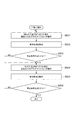
再び図1を参照し、制御部Cntの各種制御と共に、方法MTの各工程について詳細に説明する。図1に示すように、方法MTでは、まず、工程S1が実行される。工程S1では、隣接する隆起領域102の間で第2部分104bを露出させる開口が酸化領域106に形成される。図4は、図1に示す工程S1の一実施形態を示す流れ図である。以下、図4と共に、図5、図6、及び図7を参照する。図5、図6、及び図7は、図4に示す各工程に関連する被処理体の断面を示す図である。
With reference to FIG. 1 again, each step of the method MT will be described in detail along with various controls of the control unit Cnt. As shown in FIG. 1, in the method MT, step S1 is first performed. In step S <b> 1, an opening that exposes the
図4に示すように、一実施形態の工程S1は、工程SA11〜工程SA17を含んでいる。工程SA11では、図2に示すウエハWの酸化領域106を変質させることにより、変質領域が形成される。具体的に、工程SA11では、ウエハWが、第1のガスのプラズマに晒される。この第1のガスは、水素、窒素、及びフッ素を含有する。例えば、第1のガスは、H2ガス、N2ガス、及びNF3ガスの混合ガス、或いは、NH3ガス及びNF3ガスの混合ガスであり得る。また、第1のガスは、Arガスといった希ガスを含んでいてもよい。この第1のガスのプラズマにウエハWが晒されると、酸化領域106を構成する酸化シリコンが、ケイフッ化アンモニウム((NH4)2SiF6)に変質する。これにより、図5の(a)に示すように、酸化領域106の少なくとも一部が変質領域106aへと変質する。
As shown in FIG. 4, step S <b> 1 of one embodiment includes steps SA <b> 11 to SA <b> 17. In step SA11, the altered region is formed by altering the oxidized
プラズマ処理装置10を用いて工程SA11を行う場合には、制御部Cntは、ガスソース群40から上述した第1のガス供給するよう、バルブ群42及び流量制御器群44を制御する。また、制御部Cntは、第1のガスを励起させるため、高周波電力を下部電極LEに供給するよう、第1の高周波電源62を制御する。
When performing the process SA11 using the
工程SA11では、処理容器12内の圧力は、例えば、400mTorr〜600mTorr(53.33Pa〜79.99Pa)の圧力に設定される。また、第1の高周波電源62から供給される高周波電力は、例えば、800W〜1200Wの間の電力に設定される。また、工程SA11では、第2の高周波電源64からの高周波バイアス電力は供給されなくてもよい。また、第1のガスとして、H2ガス、N2ガス、及びNF3ガスの混合ガスを用いる場合には、当該混合ガス中のNF3ガスとH2ガスの分圧は、1:2〜1:10の範囲内の分圧、例えば、1:2.5の分圧に制御される。また、ウエハWの温度は、60℃以下の温度、例えば、0℃の温度に制御される。このため、制御部Cntは、プラズマ処理装置10のヒータ電源HPを制御して、載置台PDの温度を調整することができる。また、工程SA11の処理時間は、30秒〜60秒に設定され得る。
In step SA11, the pressure in the
次いで、一実施形態の工程S1では、工程SA12が行われる。工程SA12では、変質領域106aが除去される。一例では、変質領域106aは、ウエハWを加熱することによって除去される。この例では、ウエハWは、例えば60℃〜250℃の温度範囲内の温度に加熱され得る。プラズマ処理装置10においてウエハWが加熱される場合には、制御部Cntは、ヒータ電源HPを制御することにより、載置台PDの温度を調整する。これにより、ウエハWが加熱される。なお、工程SA12では、ウエハWはプラズマ処理装置10とは別の加熱処理装置を用いて加熱されてもよい。
Next, in step S1 of one embodiment, step SA12 is performed. In step SA12, the altered
また、工程SA12の別の一例では、ウエハWに対して二次電子が照射されることにより変質領域106aが除去される。この例の工程SA12をプラズマ処理装置10を用いて実行する場合には、ガスソース群40から不活性ガス又は希ガスが処理容器12内に供給され、排気装置50により処理容器12内の圧力が設定値に減圧される。なお、工程SA12で用いられるガスは、当該ガスが励起されることにより正イオンを生じさせることが可能なガスである。したがって、工程SA12では、H2ガスが用いられてもよい。また、この例の工程SA12では、電源70からプラズマ処理装置10の上部電極30に電圧が印加される。また、この例の工程SA12では、ガスを励起させるために、第1の高周波電源62から高周波電力が下部電極LEに供給される。これにより、処理容器12内において正イオンが生成される。なお、この例の工程SA12では、必要に応じて、第2の高周波電源64からの高周波バイアス電力が下部電極LEに供給されてもよい。
In another example of the process SA12, the altered
二次電子を利用する工程SA12では、処理容器12内の圧力は、例えば、40mTorr〜60mTorr(5.33Pa〜7.99Pa)の圧力に設定される。第1の高周波電源62から供給される高周波電力は、例えば、200W〜400Wの間の電力に設定される。また、第2の高周波電源64からの高周波バイアス電力は供給されなくてもよい。また、電源70からプラズマ処理装置10の上部電極30に印加される電圧は、その絶対値が1000Vの負の直流電圧であり得る。なお、工程SA12において上部電極30に印加される負の直流電圧の絶対値は、少なくとも500V以上であればよく、例えば800V〜1200Vの範囲内の絶対値に設定され得る。また、希ガスとしてArガスが供給される場合には、当該Arガスの流量は300sccm〜500sccmの範囲内の流量に設定され得る。また、ウエハWの温度は、60℃以下の温度、例えば、40℃に制御される。また、処理時間は、20秒〜40秒に設定され得る。
In process SA12 using a secondary electron, the pressure in processing
これらの例に係る工程SA12によれば、変質領域106aのケイフッ化アンモニウムが昇華する。その結果、図5の(b)に示すように、変質領域106aが除去される。
According to the process SA12 according to these examples, ammonium silicofluoride in the altered
これらの工程SA11及び工程SA12は、窒化領域104の上面が露出するまで、交互に所定回数(例えば、7回)実行される。工程SA13では、工程SA11及び工程SA12の繰り返し回数が停止条件を満たすか否かが判定される。即ち、工程SA13では、工程SA11及びSA12が所定回数実行されたか否かが判定される。この停止条件が満たされない場合には、工程SA11及び工程SA12が再び繰り返される。一方、停止条件が満たされる場合には、プロセスは工程SA14に移行する。このように工程SA11及び工程SA12が繰り返される結果、図5の(c)に示すように、酸化領域106が部分的に除去され、窒化領域104、即ち第1部分104aの上面が露出する。これら工程SA11及び工程SA12の処理は、窒化領域104に対して酸化領域106を比較的高い選択比で除去することができる。したがって、窒化領域104の損傷が抑制され得る。
These steps SA11 and SA12 are alternately performed a predetermined number of times (for example, seven times) until the upper surface of the
次いで、工程S1では、工程SA14が実行される。工程SA14では、窒化領域104及び酸化領域106上に保護膜が形成される。この工程SA14では、窒化領域104上に形成される保護膜の厚さが酸化領域106上に形成される保護膜の厚さよりも大きくなるように、保護膜の形成が調整される。
Next, in step S1, step SA14 is performed. In step SA14, a protective film is formed on the
具体的に、工程SA14では、ウエハWが第2のガスのプラズマに晒される。第2のガスは、フルオロカーボンガスを含むガスである。フルオロカーボンガスは、C4F6、C4F8、及びC6F6のうち少なくとも一種を含有するガスであり得る。また、第2のガスは、Arガスといった希ガス、及び、O2ガスを更に含み得る。工程SA14では、下部電極LEに供給される高周波バイアス電力が、後述する工程SA15において下部電極LEに供給される高周波バイアス電力よりも小さい電力となるように調整される。例えば、工程SA14では、下部電極LEに高周波バイアス電力が供給されない。これにより、窒化領域104のエッチングレートが低くなり、窒化領域104は実質的にはエッチングされなくなる。
Specifically, in step SA14, the wafer W is exposed to the plasma of the second gas. The second gas is a gas containing a fluorocarbon gas. The fluorocarbon gas may be a gas containing at least one of C 4 F 6 , C 4 F 8 , and C 6 F 6 . The second gas may further include a rare gas such as Ar gas and an O 2 gas. In step SA14, the high frequency bias power supplied to the lower electrode LE is adjusted to be lower than the high frequency bias power supplied to the lower electrode LE in step SA15 described later. For example, in step SA14, the high frequency bias power is not supplied to the lower electrode LE. As a result, the etching rate of the
また、工程SA14では、ウエハWの温度が60℃以上250℃以下の温度に設定される。これにより、図6の(a)に示すように、フルオロカーボン系の保護膜PFが窒化領域104及び酸化領域106上に形成され、酸化領域106上の保護膜PFの厚さよりも窒化領域104上の保護膜PFの厚さが大きくなる。なお、250℃を超える温度領域では、マスク108のガラス転移温度となり、また、当該温度では、酸化領域106に形成される保護膜の厚さと窒化領域104の保護膜の厚さの差が少なくなる。また、60℃より低い温度でも、酸化領域106に形成される保護膜の厚さと窒化領域104の保護膜の厚さの差が少なくなる。
In step SA14, the temperature of the wafer W is set to a temperature of 60 ° C. or higher and 250 ° C. or lower. As a result, as shown in FIG. 6A, a fluorocarbon-based protective film PF is formed on the
プラズマ処理装置10を用いて工程SA14を行う場合には、制御部Cntは、ガスソース群40から第2のガスを供給するように、バルブ群42及び流量制御器群44を制御する。また、制御部Cntは、下部電極LEに高周波電力が供給されるように第1の高周波電源62を制御する。また、制御部Cntは、高周波バイアス電力が低い電力となるように、例えば、高周波バイアス電力が供給されないように、第2の高周波電源64を制御する。また、制御部Cntは、プラズマ処理装置10のヒータ電源HPを制御することにより、載置台PDの温度を調整し、これによりウエハWの温度を調整する。
When performing the process SA14 using the
例えば、工程SA14では、処理容器12内の圧力は、10mTorr〜30mTorr(1.333Pa〜4Pa)の圧力に設定される。また、工程SA14では、第1の高周波電源62から、60MHz且つ500W〜2000Wの高周波電力が下部電極LEに供給される。また、第2のガス中のC4F6ガス、Arガス、O2ガスの流量はそれぞれ、15sccm〜25sccmの流量、500sccm〜600sccmの流量、10sccm〜20sccmの流量に設定される。また、工程SA14の処理時間は、10秒〜20秒であり得る。
For example, in step SA14, the pressure in the
次いで、工程S1では、工程SA15が実行される。工程SA15では、酸化領域106がエッチングされる。本例においては、隣接する隆起領域102の間に存在する酸化領域106がエッチングされる。
Next, in step S1, step SA15 is performed. In step SA15, the oxidized
具体的に、工程SA15では、第3のガスのプラズマに晒される。第3のガスは、フルオロカーボンガスを含むガスである。フルオロカーボンガスは、C4F6、C4F8、及びC6F6のうち少なくとも一種を含有するガスであり得る。また、第3のガスは、Arガスといった希ガス、及び、O2ガスを更に含み得る。工程SA15では、下部電極LEに比較的高い高周波バイアス電力が供給される。これにより、比較的薄い保護膜PFがその上に形成されている酸化領域106が、図6の(b)に示すように、エッチングされる。
Specifically, in step SA15, the substrate is exposed to the third gas plasma. The third gas is a gas containing a fluorocarbon gas. The fluorocarbon gas may be a gas containing at least one of C 4 F 6 , C 4 F 8 , and C 6 F 6 . The third gas may further include a rare gas such as Ar gas and an O 2 gas. In step SA15, a relatively high high-frequency bias power is supplied to the lower electrode LE. As a result, the oxidized
プラズマ処理装置10を用いて工程SA15を行う場合には、制御部Cntは、ガスソース群40から第3のガスを供給するように、バルブ群42及び流量制御器群44を制御する。また、制御部Cntは、下部電極LEに高周波電力が供給されるように第1の高周波電源62を制御する。また、制御部Cntは、下部電極LEに高周波バイアス電力が供給されるように第2の高周波電源64を制御する。
When performing the process SA15 using the
例えば、工程SA15では、処理容器12内の圧力は、10mTorr〜30mTorr(1.333Pa〜4Pa)の圧力に設定される。また、工程SA15では、第1の高周波電源62から、60MHz且つ500W〜2000Wの高周波電力が下部電極LEに供給される。また、工程SA15では、第2の高周波電源64から、1000W〜2000Wの高周波バイアス電力が下部電極LEに供給される。また、第3のガス中のC4F6ガス、Arガス、O2ガスの流量はそれぞれ、15sccm〜25sccmの流量、500sccm〜600sccmの流量、10sccm〜20sccmの流量に設定される。また、工程SA15の処理時間は、10秒〜30秒であり得る。なお、工程SA15におけるウエハWの温度は、工程SA14におけるウエハWの温度と同じ温度であってもよく、或いは、工程SA14のウエハWの温度よりも低い温度であってもよい。
For example, in step SA15, the pressure in the
これらの工程SA14及び工程SA15は交互に所定回数実行される。工程SA16では、工程SA14及び工程SA15の繰り返し回数が停止条件を満たすか否かが判定される。即ち、工程SA16では、工程SA14及びSA15が所定回数実行されたか否かが判定される。この停止条件が満たされない場合には、工程SA14及び工程SA15が再び繰り返される。一方、停止条件が満たされる場合には、工程SA14及び工程SA15の実行が終了する。このように工程SA14及び工程SA15が交互に所定回数実行されることにより、図6の(c)に示すように、隣接する隆起領域102の間に存在する酸化領域106が、ある深さまでエッチングされる。なお、図6の(c)では、酸化領域106のエッチングは窒化領域104の第2部分104bの上面まで達していないが、工程SA14及び工程SA15は、酸化領域106のエッチングが第2部分104bの上面に達するまで実行されてもよい。
These steps SA14 and SA15 are alternately executed a predetermined number of times. In Step SA16, it is determined whether or not the number of repetitions of Step SA14 and Step SA15 satisfies the stop condition. That is, in step SA16, it is determined whether or not steps SA14 and SA15 have been executed a predetermined number of times. If this stop condition is not satisfied, Step SA14 and Step SA15 are repeated again. On the other hand, when the stop condition is satisfied, the execution of step SA14 and step SA15 ends. As shown in FIG. 6C, the oxidized
これらの工程SA14及び工程SA15によれば、露出直後において保護膜が形成されていない窒化領域104の削れを抑制しつつ、酸化領域106をエッチングすることが可能となる。かかる工程SA14及び工程SA15を所定回数実行すると、窒化領域104上では保護膜PFが維持される。また、フルオロカーボンを含有するガスのエッチングでは、酸化領域106上への保護膜の形成と酸化領域106のエッチングとが同時に進行する。したがって、工程SA14及び工程SA15を所定回数実行した後に、工程SA15と同様のエッチングを実行することによって、酸化領域106を更にエッチングすることができる。これにより、酸化領域106のエッチングレートを高めることが可能である。
According to these step SA14 and step SA15, the oxidized
具体的には、工程SA16に続いて、工程SA17を実行することができる。工程SA17では、工程SA15と同様の条件で、隣接する隆起領域102の間に存在する酸化領域106のエッチングが進められる。この工程SA17をプラズマ処理装置10を用いて行う場合には、制御部Cntは、工程SA15における制御と同様の制御を実行することができる。この工程SA17を行うと図7の(a)に示すように、ウエハWには、第2部分104bを露出させる開口OPが形成される。但し、図7の(a)に示すように、第2部分104bと第1部分104aによって囲まれた隅部には、酸化シリコンから構成された残渣106bが残される。この残渣106bの除去については後述する。
Specifically, step SA17 can be executed subsequent to step SA16. In step SA17, etching of the oxidized
以下、工程S1の別の実施形態について説明する。図8は、図1に示す工程S1の別の実施形態を示す流れ図である。図8に示すように、別の実施形態では、工程S1は、上述した工程SA11、工程SA12、及び工程SA13に加えて、工程SB14及び工程SB15を含んでいる。以下、図8と共に、図9を参照して工程SB14及び工程SB15について説明する。図9は、図8に示す各工程に関連する被処理体の断面を示す図である。 Hereinafter, another embodiment of the step S1 will be described. FIG. 8 is a flowchart showing another embodiment of step S1 shown in FIG. As shown in FIG. 8, in another embodiment, step S1 includes step SB14 and step SB15 in addition to step SA11, step SA12, and step SA13 described above. Hereinafter, the process SB14 and the process SB15 will be described with reference to FIG. 9 together with FIG. FIG. 9 is a view showing a cross section of an object to be processed related to each step shown in FIG.
図8に示す工程S1では、工程SA11及び工程SA12の所定回数の実行により、ウエハWは、図5の(c)に示す状態となる。図8に示す工程S1では、この状態のウエハWに対して、工程SB14及び工程SB15が所定回数実行される。 In step S1 shown in FIG. 8, the wafer W is in the state shown in FIG. 5C by executing the steps SA11 and SA12 a predetermined number of times. In step S1 shown in FIG. 8, step SB14 and step SB15 are performed a predetermined number of times on the wafer W in this state.
工程SB14では、ウエハWがフルオロカーボンガスを含む第4のガスのプラズマに晒される。工程SB14では、第4のガスが励起されることによりプラズマが生成され、生成されたプラズマにウエハWが晒される。第4のガスは、フルオロカーボンガスを含むガスである。フルオロカーボンガスは、C4F6、C4F8、及びC6F6のうち少なくとも一種を含有するガスであり得る。また、第4のガスは、Arガスといった希ガス、及び、O2ガスを更に含み得る。 In step SB14, the wafer W is exposed to a plasma of a fourth gas containing a fluorocarbon gas. In step SB14, the fourth gas is excited to generate plasma, and the wafer W is exposed to the generated plasma. The fourth gas is a gas containing a fluorocarbon gas. The fluorocarbon gas may be a gas containing at least one of C 4 F 6 , C 4 F 8 , and C 6 F 6 . The fourth gas may further include a rare gas such as Ar gas and O 2 gas.
プラズマ処理装置10を用いて工程SB14を実行する場合には、ガスソース群40から第4のガスが処理容器12内に供給される。また、工程SB14では、第1の高周波電源62からの高周波電力が下部電極LEに供給される。また、工程SB14では、第2の高周波電源64からの高周波バイアス電力が下部電極LEに供給され得る。また、工程SB14では、排気装置50によって処理容器12内の空間の圧力が所定の圧力に設定される。例えば、処理容器12内の空間の圧力は、20mTorr(2.666Pa)〜50mTorr(6.666Pa)の範囲内の圧力に設定される。さらに、工程SB14では、上部電極30と載置台PDの上面との間の距離が、20mm〜50mmの範囲内の距離に設定される。これにより、処理容器12内においてフルオロカーボンガスのプラズマが生成され、載置台PD上に載置されたウエハWが当該プラズマに晒される。なお、工程SB14では、上部電極30に電源70からの電圧が印加されてもよい。電源70によって上部電極30に印加される電圧は、−150V以下の電圧であり得る。即ち、電源70によって上部電極30に印加される電圧は、絶対値が150V以上の負の電圧であり得る。この工程SB14の実行時のプラズマ処理装置10の各部の動作は、制御部Cntによって制御され得る。
When the process SB <b> 14 is performed using the
工程SB14では、初期的には図5の(c)に示す状態を有するウエハWの酸化領域106に、フルオロカーボンに由来する原子及び/又は分子の活性種、例えば、フッ素及び/又はフルオロカーボンの活性種が衝突する。これにより、工程SB14では、酸化領域106がエッチングされる。また、工程SB14では、図9の(a)に示すように、フルオロカーボンを含む堆積物が酸化領域106に付着する。これにより、フルオロカーボンを含む堆積物DPが酸化領域106上に形成される。この堆積物DPの膜厚は、工程SB14の実行時間の経過につれて増加する。
In step SB14, an active species of atoms and / or molecules derived from fluorocarbon, for example, active species of fluorine and / or fluorocarbon, is initially formed in the oxidized
また、工程SB14では、初期的には図5の(c)に示すウエハWの窒化領域104にも、フルオロカーボンに由来する原子及び/又は分子の活性種、例えば、フッ素及び/又はフルオロカーボンの活性種が衝突する。かかる活性種が窒化領域104に衝突すると、図9の(a)に示すように、窒化領域104の表面からある深さの表層部分が改質され、改質領域TRが形成され得る。改質領域TRは、窒化領域104を構成するシリコン及び窒素、第4のガスに含まれる原子及び/又は分子を含有する。例えば、改質領域TRは、シリコン及び窒素に加えて、第4のガスに含まれる炭素、フッ素、及び酸素を含有し得る。また、工程SB14では、改質領域TR上に堆積物DPが形成される。
Further, in step SB14, initially, the active species of atoms and / or molecules derived from fluorocarbon, for example, active species of fluorine and / or fluorocarbon are also present in the
なお、工程SB14において電源70からの電圧が上部電極30に印加される場合には、処理空間Sに存在する正イオンが、電極板34に衝突する。これにより、電極板34からシリコンが放出される。放出されたシリコンは、処理空間S内に存在するフッ素の活性種、例えば、フッ素ラジカル及びフッ素イオンと結合し、フッ素の活性種の量を低減させる。これにより、フッ素の活性種による窒化領域104のエッチングが抑制される。一方、酸化領域106はプラズマ中のフルオロカーボンの活性種によってエッチングされる。
When a voltage from the
このような工程SB14の処理により形成された堆積物DPの膜厚が大きくなると、酸化領域106をエッチングし得る活性種が酸化領域106に到達することが当該堆積物DPによって阻害される。したがって、工程SB14を連続的に継続すると、酸化領域106のエッチングが停止する。このようなエッチングの停止を防止するために、次いで、工程SB15が実行される。
When the film thickness of the deposit DP formed by the process in the step SB14 is increased, the deposit DP prevents the active species that can etch the oxidized
工程SB15では、堆積物DPに含まれるフルオロカーボンのラジカルにより酸化領域106がエッチングされる。一実施形態の工程SB15では、工程SB14の処理後のウエハWが、希ガスのプラズマに晒される。この工程SB15の処理時間と工程SB14の処理時間は任意に設定され得る。一実施形態においては、工程SB14の処理時間と工程SB15の処理時間の合計において工程SB14の処理時間が占める割合は、30%〜70%の範囲内の割合に設定され得る。
In step SB15, the oxidized
プラズマ処理装置10を用いて工程SB15を実行する場合には、ガスソース群40から希ガスが供給される。また、工程SB15では、希ガスに加えて酸素ガス(O2ガス)が供給されてもよく、或いは、酸素ガスが供給されなくてもよい。また、工程SB15では、第1の高周波電源62からの高周波電力が下部電極LEに供給される。また、工程SB15では、第2の高周波電源64からの高周波バイアス電力が下部電極LEに供給され得る。また、工程SB15では、排気装置50によって処理容器12内の空間の圧力が所定の圧力に設定される。例えば、処理容器12内の空間の圧力は、20mTorr(2.666Pa)〜50mTorr(6.666Pa)の範囲内の圧力に設定される。さらに、工程SB15では、上部電極30と載置台PDの上面との間の距離が、20mm〜50mmの範囲内の距離に設定される。これにより、処理容器12内において希ガスのプラズマが生成され、載置台PD上に載置されたウエハWが当該プラズマに晒される。なお、工程SB15では、上部電極30に電源70からの電圧が印加されてもよい。電源70によって上部電極30に印加される電圧は、−150V以下の電圧であり得る。即ち、電源70によって上部電極30に印加される電圧は、絶対値が150V以上の負の電圧であり得る。この工程SB15の実行時のプラズマ処理装置10の各部の動作は、制御部Cntによって制御され得る。
When the process SB15 is performed using the
工程SB15では、希ガス原子の活性種、例えば、希ガス原子のイオンが、堆積物DPに衝突する。これにより、図9の(b)に示すように、堆積物DP中のフルオロカーボンラジカルが、酸化領域106のエッチングを進行させる。また、この工程SB15により、堆積物DPの膜厚が減少する。また、工程SB15では、図9の(b)に示すように、窒化領域104上の堆積物DPの膜厚も減少する。ただし、窒化領域104上には改質領域TRが存在するので、窒化領域104のエッチングは抑制される。
In step SB15, active species of rare gas atoms, for example, ions of rare gas atoms collide with the deposit DP. As a result, as shown in FIG. 9B, the fluorocarbon radicals in the deposit DP advance the etching of the oxidized
なお、工程SB15において電源70からの電圧が上部電極30に印加される場合には、処理空間Sに存在する正イオンが、電極板34に衝突する。これにより、電極板34からシリコンが放出される。工程SB15の実行期間中には、工程SB14において生成されたフッ素の活性種が除去されずに処理容器12内に残存し得る。電極板34から放出されたシリコンは、処理空間S内に存在するフッ素の活性種と結合し、フッ素の活性種の量を低減させる。これにより、フッ素の活性種による窒化領域104のエッチングが抑制される。一方、酸化領域106は堆積物DP中のフルオロカーボンラジカルによってエッチングされる。また、工程SB15において酸素ガスが供給されない場合には、酸化領域106が窒化領域104に対して更に選択的にエッチングされ得る。
When a voltage from the
図8に示す工程S1では、工程SB15の実行の後、再び、工程SB14が実行される。先の工程SB15の実行によって堆積物DPの膜厚が減少しているので、再び工程SB14を実行して第4のガスのプラズマにウエハWを晒すと、酸化領域106を更にエッチングすることができる。その後、更に工程SB15を実行することで、堆積物DP中のフルオロカーボンラジカルにより酸化領域106をエッチングすることができる。
In step S1 shown in FIG. 8, step SB14 is performed again after step SB15. Since the film thickness of the deposit DP has decreased due to the execution of the previous step SB15, the oxidized
図8に示す工程S1では、工程SB16において停止条件が満たされるか否かが判定される。停止条件は、例えば、工程SB14及び工程SB15を含むサイクルの繰り返し回数が所定回数に達したときに満たされたものと判定される。停止条件が満たされない場合には、工程SB14及び工程SB15を含むサイクルが再び実行される。一方、停止条件が満たされる場合には、工程S1が終了する。 In step S1 shown in FIG. 8, it is determined whether or not the stop condition is satisfied in step SB16. For example, the stop condition is determined to be satisfied when the number of repetitions of the cycle including the process SB14 and the process SB15 reaches a predetermined number. When the stop condition is not satisfied, the cycle including the process SB14 and the process SB15 is executed again. On the other hand, when the stop condition is satisfied, the process S1 ends.
図8に示す工程S1によれば、工程SB14及び工程SB15を交互に複数回実行することにより、酸化領域106のエッチングの停止を防止することができる。その結果、酸化領域106のエッチングを継続することができる。さらに、酸化領域106を窒化領域104に対して選択的にエッチングすることができる。かかる工程S1の実行により、ウエハWは、図7の(a)に示す状態となる。
According to step S1 shown in FIG. 8, the stop of etching of the oxidized
再び図1を参照する。方法MTでは、次いで、工程S2が実行される。工程S2では、マスク108が除去される。マスク108は、酸素ガスのプラズマを用いたアッシング処理によって除去される。この工程S2では、ウエハW上に堆積している堆積物、即ち、フルオロカーボンを含有する堆積物も除去される。即ち、工程S2では、ウエハW上の有機物が除去される。この工程S2により、ウエハWは図7の(b)に示した状態となる。プラズマ処理装置10において工程S2を実行する場合には、制御部Cntは、酸素ガスを処理容器12内に供給するよう、バルブ群42及び流量制御器群44を制御する。また、制御部Cntは、処理容器12内に供給されたガスを励起させるため、高周波電力を下部電極LEに供給するよう、第1の高周波電源62を制御する。また、制御部Cntは、高周波バイアス電力を下部電極LEに供給するよう、第2の高周波電源64を制御してもよい。
Refer to FIG. 1 again. In method MT, step S2 is then performed. In step S2, the
方法MTでは、次いで、工程S3が実行される。工程S3では、残渣106b及び第2部分104bがエッチングされる。このため、ウエハWは、水素を含有するガス及びNF 3 ガスを含む混合ガスのプラズマに晒される。これにより、変質領域が形成される。そして、変質領域が除去される。
In method MT, step S3 is then performed. In step S3, the
以下、図10及び図11を参照して、工程S3の一実施形態について詳細に説明する。図10は、図1に示す工程S3の一実施形態を示す流れ図である。図11は、図10に示す各工程に関連する被処理体の断面を示す図である。 Hereinafter, with reference to FIG.10 and FIG.11, one Embodiment of process S3 is described in detail. FIG. 10 is a flowchart showing an embodiment of step S3 shown in FIG. FIG. 11 is a view showing a cross section of the object to be processed related to each step shown in FIG.
図10に示すように、一実施形態の工程S3は、工程SA21及び工程SA22を含んでいる。工程SA21では、図7の(b)に示す状態のウエハWが、H2ガス及びNF3ガスを含む第5のガス(混合ガス)のプラズマに晒される。この第5のガスは、更にN2ガス、及びArガスといった希ガスを含んでいてもよい。この工程SA21では、第5のガスのプラズマが生成されることにより、フッ化アンモニウム、フッ素の活性種、及び、HFの活性種が生成される。フッ化アンモニウムは残渣106bを構成する酸化シリコンと反応する。これにより、図11の(a)に示すように、残渣106bを構成する酸化シリコンがケイフッ化アンモニウムに変質して、当該残渣106bから変質領域106cが形成される。また、HFの活性種は第2部分104bを構成する窒化シリコンと反応する。これにより、第2部分104bを構成する窒化シリコンがケイフッ化アンモニウムに変質して、当該第2部分104bから変質領域104cが形成される。
As shown in FIG. 10, step S3 of one embodiment includes step SA21 and step SA22. In step SA21, the wafer W in the state shown in FIG. 7B is exposed to plasma of a fifth gas (mixed gas) containing H 2 gas and NF 3 gas. The fifth gas may further contain a rare gas such as N 2 gas and Ar gas. In this step SA21, the fifth gas plasma is generated to generate ammonium fluoride, fluorine active species, and HF active species. Ammonium fluoride reacts with silicon oxide constituting the
プラズマ処理装置10を用いて工程SA21を行う場合には、制御部Cntは、ガスソース群40から第5のガスを供給するようにバルブ群42及び流量制御器群44を制御する。また、制御部Cntは、第5のガスを励起させるため、高周波電力を下部電極LEに供給するように第1の高周波電源62を制御する。
When performing the process SA21 using the
工程SA21では、処理容器12内の圧力は、例えば、400mTorr〜600mTorr(53.33Pa〜79.99Pa)の圧力に設定される。また、第1の高周波電源62から供給される高周波電力は、例えば、800W〜1200Wの間の電力に設定される。また、工程SA21では、第2の高周波電源64からの高周波バイアス電力は供給されなくてもよい。また、第5のガス中のNF3ガスとH2ガスの分圧は、1:2〜1:10の範囲内の分圧、例えば、1:2.5の分圧に制御される。また、ウエハWの温度は、60℃以下の温度、例えば、0℃の温度に制御される。このため、制御部Cntは、プラズマ処理装置10のヒータ電源HPを制御して、載置台PDの温度を調整することができる。また、工程SA21の処理時間は、30秒〜60秒に設定され得る。
In step SA21, the pressure in the
続く工程SA22では、変質領域106c及び変質領域104cが除去される。変質領域106c及び変質領域104cの除去のために行われる処理は、上述した工程SA12と同様である。また、工程SA22をプラズマ処理装置10を用いて実行する場合には、制御部Cntは、工程SA12における制御と同様の制御を実行する。この工程SA22が実行されることにより、図11の(b)に示すように、酸化領域106の上面から隣接する隆起領域102の間を通って下地層100の上面まで達するホールHLが形成される。
In the subsequent step SA22, the altered
これらの工程SA21及び工程SA22は、交互に所定回数実行されてもよい。工程SA23では、工程SA21及び工程SA22の繰り返し回数が停止条件を満たすか否かが判定される。即ち、工程SA23では、工程SA21及びSA22が所定回数実行されたか否かが判定される。この停止条件が満たされない場合には、工程SA21及び工程SA22が再び繰り返される。一方、停止条件が満たされる場合には、工程S3が終了する。即ち、方法MTが終了する。 These step SA21 and step SA22 may be alternately executed a predetermined number of times. In Step SA23, it is determined whether or not the number of repetitions of Step SA21 and Step SA22 satisfies the stop condition. That is, in step SA23, it is determined whether or not steps SA21 and SA22 have been executed a predetermined number of times. If this stop condition is not satisfied, Step SA21 and Step SA22 are repeated again. On the other hand, when the stop condition is satisfied, the process S3 ends. That is, the method MT ends.
なお、従来から用いられているフルオロカーボンガスのプラズマでは、残渣106bを除去できないので、第2部分104bを除去するまでに、第1部分104a、特に第1部分104aの肩部104s(図11の(b)を参照)が、フッ素の活性種又はHFの活性種によって大きく削られてしまう。一方、図10に示す実施形態の工程S3によれば、残渣106bが除去されるので、第1部分104a、特に肩部104sの削れを低減することができる。また、図10に示す実施形態の工程S3によれば、残渣106b及び第2部分104bを一括して除去することが可能である。
Since the
以下、図12、図13、及び図14を参照して、工程S3の別の実施形態について詳細に説明する。図12は、図1に示す工程S3の別の実施形態を示す流れ図である。図13及び図14は、図12に示す各工程に関連する被処理体の断面を示す図である。 Hereinafter, with reference to FIG. 12, FIG. 13, and FIG. 14, another embodiment of the step S3 will be described in detail. FIG. 12 is a flowchart showing another embodiment of step S3 shown in FIG. 13 and 14 are views showing cross sections of the object to be processed related to the respective steps shown in FIG.
図12に示すように、一実施形態の工程S3は、工程SB21〜工程SB26を含んでいる。工程SB21では、図7の(b)に示す状態のウエハWが、NH3ガス及びNF3ガスを含む第6のガス(混合ガス)のプラズマに晒される。この第6のガスは、更にArガスといった希ガスを含んでいてもよい。この工程SB21により、図13の(a)に示すように、残渣106bを構成する酸化シリコンがケイフッ化アンモニウムに変質して、変質領域106cが形成される。
As illustrated in FIG. 12, the process S3 of one embodiment includes processes SB21 to SB26. In step SB21, the wafer W in the state shown in FIG. 7B is exposed to plasma of a sixth gas (mixed gas) containing NH 3 gas and NF 3 gas. The sixth gas may further contain a rare gas such as Ar gas. Through this step SB21, as shown in FIG. 13A, the silicon oxide constituting the
上述した第5のガス、即ち、H2ガス及びNF3ガスに比べて、第6のガス、即ち、NH3ガス及びNF3ガスを含むガスは、低解離のプラズマを発生させることによってフッ化アンモニウムを生成することができる。したがって、第5のガスに比べて、第6のガスによれば、プラズマ中でのフッ素の活性種及びHFの活性種の発生量が低減される。その結果、第2部分104bの変質及び削れを抑制しつつ、残渣106bを変質させて、変質領域106cを形成することができる。
Compared to the fifth gas described above, that is, H 2 gas and NF 3 gas, the sixth gas, that is, gas containing NH 3 gas and NF 3 gas, is fluorinated by generating low dissociation plasma. Ammonium can be produced. Therefore, compared to the fifth gas, according to the sixth gas, the generation amount of the active species of fluorine and the active species of HF in the plasma is reduced. As a result, the altered
プラズマ処理装置10を用いて工程SB21を行う場合には、制御部Cntは、ガスソース群40から第6のガスを供給するようにバルブ群42及び流量制御器群44を制御する。また、制御部Cntは、第6のガスを励起させるため、高周波電力を下部電極LEに供給するように第1の高周波電源62を制御する。
When performing step SB21 using the
工程SB21では、処理容器12内の圧力は、例えば、400mTorr〜600mTorr(53.33Pa〜79.99Pa)の圧力に設定される。また、第1の高周波電源62から供給される高周波電力は、例えば、800W〜1200Wの間の電力に設定される。また、工程SB21では、第2の高周波電源64からの高周波バイアス電力は供給されなくてもよい。また、ウエハWの温度は、60℃以下の温度、例えば、0℃の温度に制御される。このため、制御部Cntは、プラズマ処理装置10のヒータ電源HPを制御して、載置台PDの温度を調整することができる。また、工程SB21の処理時間は、30秒〜60秒に設定され得る。
In step SB21, the pressure in the
続く工程SB22では、変質領域106cが除去される。変質領域106cの除去のために行われる処理は、上述した工程SA12と同様である。また、工程SB22をプラズマ処理装置10を用いて実行する場合には、制御部Cntは、工程SA12における制御と同様の制御を実行する。この工程SB22が実行されることにより、図13の(b)に示すように、変質領域106cが除去される。即ち、残渣106bが除去される。
In the subsequent step SB22, the altered
これらの工程SB21及び工程SB22は、交互に所定回数実行されてもよい。工程SB23では、工程SB21及び工程SB22の繰り返し回数が停止条件を満たすか否かが判定される。即ち、工程SB23では、工程SB21及びSB22が所定回数実行されたか否かが判定される。この停止条件が満たされない場合には、工程SB21及び工程SB22が再び繰り返される。一方、停止条件が満たされる場合には、プロセスは工程SB24に移行する。 These process SB21 and process SB22 may be alternately executed a predetermined number of times. In step SB23, it is determined whether or not the number of repetitions of step SB21 and step SB22 satisfies the stop condition. That is, in step SB23, it is determined whether or not steps SB21 and SB22 have been executed a predetermined number of times. If this stop condition is not satisfied, step SB21 and step SB22 are repeated again. On the other hand, when the stop condition is satisfied, the process proceeds to step SB24.
工程SB24では、図13の(b)に示す状態のウエハWが、第5のガスのプラズマに晒される。工程SB24の処理は、上述した工程SA21と同様の処理である。この工程SB24が実行されることにより、第2部分104bを構成する窒化シリコンがケイフッ化アンモニウムに変質する。これにより、図14の(a)に示すように、第2部分104bから変質領域104cが形成される。
In step SB24, the wafer W in the state shown in FIG. 13B is exposed to the plasma of the fifth gas. The process of step SB24 is the same as the process S A 21 described above. By performing this step SB24, the silicon nitride constituting the
続く工程SB25では、変質領域104cが除去される。変質領域104cの除去のために行われる処理は、上述した工程SA12と同様である。また、工程SB25をプラズマ処理装置10を用いて実行する場合には、制御部Cntは、工程SA12における制御と同様の制御を実行する。かかる工程SB25が実行されることにより、図14の(b)に示すように、変質領域104cが除去される。即ち、第2部分104bが除去される。その結果、図14の(b)に示すように、酸化領域106の上面から隣接する隆起領域102の間を通って下地層100の上面まで達するホールHLが自己整合的に形成される。
In the subsequent step SB25, the altered
図12に示す実施形態の工程S3によれば、残渣106bの除去時には、低解離状態のプラズマを発生させることによりフッ化アンモニウムを生成することが可能な第6のガスが用いられれる。したがって、残渣106bの除去が行われている期間中の第1部分104aの削れを抑制することができる。次いで、H2ガス及びNF3ガスを含む第5のガスを用いることにより、第2部分104bのエッチングレートを高めることができる。したがって、図12に示す実施形態の工程S3によれば、第1部分104aの削れを更に低減しつつ、残渣106b及び第2部分104bを除去することが可能となる。
According to step S3 of the embodiment shown in FIG. 12, at the time of removing the
以下、別の実施形態に係る被処理体を処理する方法について、図15を参照しつつ説明する。図15は、別の実施形態に係る被処理体を処理する方法を示す流れ図である。図16は、図15に示す方法の幾つかの工程に関連する被処理体の断面を示す図である。図15に示す方法MT2は、工程S2と工程S3との間に実行される工程S4を含む点で方法MTとは、異なっている。 Hereinafter, a method of processing an object to be processed according to another embodiment will be described with reference to FIG. FIG. 15 is a flowchart illustrating a method for processing an object to be processed according to another embodiment. FIG. 16 is a view showing a cross section of an object to be processed related to several steps of the method shown in FIG. The method MT2 shown in FIG. 15 is different from the method MT in that it includes a step S4 executed between the step S2 and the step S3.
工程S4では、第1部分104a及び第2部分104b上に保護膜PF2が形成される。この保護膜PF2の形成のために、工程S4では、フルオロカーボンガスを含む処理ガスのプラズマが生成され、工程S2の実行後のウエハW、即ち、図7の(b)に示すウエハWが当該プラズマによって処理される。フルオロカーボンガスとしては、C4F6、C4F8、C6F6、C3F8、及びC5F8のうち少なくとも一種を含むガスが用いられる。また、工程S4に用いられる処理ガスは、Arガスといった希ガスを更に含み得る。この処理ガスの全流量に対するフルオロカーボンガスの流量の割合は、1%以下の割合であってもよく、残りの割合は希ガスが占めていてもよい。なお、工程S4において保護膜PF2の形成のために使用される処理ガスは、フルオロカーボンガスに代えて、ハイドロフルオロカーボンガス、又はシリコン含有ガスを含んでいてもよい。ハイドロフルオロカーボンガスとしては、CH2F2又はCHF3を含むガスが例示される。また、シリコン含有ガスとしては、SiF4とH2を含むガス、又は、SiCl4とH2を含むガスが例示される。
In step S4, the protective film PF2 is formed on the
プラズマ処理装置10を用いて工程S4を行う場合には、制御部Cntは、ガスソース群40からフルオロカーボンガスを含む処理ガスを供給するように、バルブ群42及び流量制御器群44を制御する。また、制御部Cntは、下部電極LEに高周波電力が供給されるように第1の高周波電源62を制御する。また、制御部Cntは、高周波バイアス電力が低い電力となるように、例えば、高周波バイアス電力が供給されないように、第2の高周波電源64を制御する。なお、例えば、工程S4において下部電極LEに供給される高周波電力は、500Wであり、工程S4における処理容器12内の圧力は、30mTorr(4Pa)であり得る。
When performing step S <b> 4 using the
工程S4では、図16の(a)に示すように、フルオロカーボンの分子によって保護膜PF2が、第1部分104a、第2部分104b、及び、残渣106b上に形成される。保護膜PF2の形成に寄与する分子の量は、隆起領域102の頂部近傍、即ち開口OPの開口端近傍では多く、開口OPの深部では少なくなる。したがって、保護膜PF2の膜厚は、隆起領域102の頂部近傍で大きくなり、開口OPの深部近傍では小さくなる。即ち、第1部分104a上では保護膜PF2の膜厚は大きくなり、残渣106b及び第2部分104b上では保護膜PF2の膜厚は小さくなる。
In step S4, as shown in FIG. 16A, the protective film PF2 is formed on the
方法MT2では、かかる保護膜PF2が形成された後に、工程S3が実行される。上述したように、第1部分104a上では保護膜PF2の膜厚は大きく、残渣106b及び第2部分104b上では保護膜PF2の膜厚は小さいので、工程S3の実行時には、第2部分104b及び残渣106b上に形成された保護膜PF2は、早期に消失し、残渣106b及び第2部分104bはエッチングされる。一方、第1部分104a上に形成された保護膜PF2は、工程S3の実行期間中において維持される。したがって、図16の(b)に示すように、工程S3の実行による第1部分104aの削れ、特に肩部104sの削れが更に抑制される。
In the method MT2, step S3 is performed after the protective film PF2 is formed. As described above, since the thickness of the protective film PF2 is large on the
なお、工程S4の実行と工程S3における変質領域の形成及び変質領域の除去を含むシーケンスの1回以上の実行とが交互に行われてもよい。図17及び図18は、更に別の実施形態に係る被処理体を処理する方法を示す流れ図である。図17に示す方法MT3では、工程S4の実行後、図10を参照して説明した工程SA21及び工程SA22を含むシーケンスSQの実行が1回以上行われる。方法MT3では、工程S4の実行と1回以上のシーケンスSQの実行とが交互に所定回数行われる。工程S5において停止条件が満たされない、即ち、工程S4の実行と1回以上のシーケンスSQの実行との交互の繰り返しの回数が所定回数に至っていないと判定される場合には、工程S4が再び実行される。一方、工程S5において、停止条件が満たされる、即ち、工程S4の実行と1回以上のシーケンスSQの実行との交互の繰り返しの回数が所定回数に至っていると判定される場合には、方法MT3が終了する。 The execution of step S4 and the execution of the sequence including the formation of the altered region and the removal of the altered region in step S3 may be performed alternately. 17 and 18 are flowcharts showing a method of processing an object to be processed according to still another embodiment. In the method MT3 shown in FIG. 17, after the execution of the step S4, the execution of the sequence SQ including the step SA21 and the step SA22 described with reference to FIG. 10 is performed once or more. In method MT3, execution of step S4 and execution of one or more sequences SQ are alternately performed a predetermined number of times. If it is determined in step S5 that the stop condition is not satisfied, that is, it is determined that the number of alternate repetitions of execution of step S4 and execution of one or more sequences SQ has not reached the predetermined number, step S4 is executed again. Is done. On the other hand, when it is determined in step S5 that the stop condition is satisfied, that is, it is determined that the number of alternate repetitions of execution of step S4 and execution of one or more sequences SQ has reached a predetermined number of times, method MT3 Ends.
図18に示す方法MT4では、工程S4の実行後、図12を参照して説明した工程SB21及び工程SB22を含むシーケンスSQ1の実行が1回以上行われる。方法MT4では、工程S4の実行と1回以上のシーケンスSQ1の実行とが交互に所定回数行われる。工程S6において、停止条件が満たされない、即ち、工程S4の実行と1回以上のシーケンスSQ1の実行との交互の繰り返しの回数が所定回数に至っていないと判定される場合には、工程S4が再び実行される。一方、工程S6において、停止条件が満たされる、即ち、工程S4の実行と1回以上のシーケンスSQ1の実行との交互の繰り返しの回数が所定回数に至っていると判定される場合には、工程S4の実行と、図12を参照して説明した工程SB24及び工程SB25を含むシーケンスSQ2の1回以上の実行とが交互に所定回数行われる。工程S7において、停止条件が満たされない、即ち、工程S4の実行と1回以上のシーケンスSQ2の実行との交互の繰り返しの回数が所定回数に至っていないと判定される場合には、工程S4が再び実行される。一方、工程S7において、停止条件が満たされる、即ち、工程S4の実行と1回以上のシーケンスSQ2の実行との交互の繰り返しの回数が所定回数に至っていると判定される場合には、方法MT4が終了する。 In the method MT4 shown in FIG. 18, the execution of the sequence SQ1 including the step SB21 and the step SB22 described with reference to FIG. In method MT4, execution of step S4 and execution of one or more sequences SQ1 are alternately performed a predetermined number of times. In step S6, when it is determined that the stop condition is not satisfied, that is, it is determined that the number of alternate repetitions of execution of step S4 and execution of one or more sequences SQ1 has not reached the predetermined number, step S4 is performed again. Executed. On the other hand, if it is determined in step S6 that the stop condition is satisfied, that is, it is determined that the number of alternate repetitions of execution of step S4 and execution of one or more sequences SQ1 has reached a predetermined number of times, step S4 And one or more executions of the sequence SQ2 including the process SB24 and the process SB25 described with reference to FIG. 12 are alternately performed a predetermined number of times. If it is determined in step S7 that the stop condition is not satisfied, that is, it is determined that the number of alternate repetitions of execution of step S4 and execution of one or more sequences SQ2 has not reached the predetermined number, step S4 is performed again. Executed. On the other hand, when it is determined in step S7 that the stop condition is satisfied, that is, it is determined that the number of alternate repetitions of execution of step S4 and execution of one or more sequences SQ2 has reached a predetermined number, method MT4 Ends.
以下、上述した種々の実施形態に係る方法の評価のために行った実験例1について説明する。この実験例1では、図2に示すウエハWを処理対象として、図3に示すプラズマ処理装置10を用いて、図1、図4、及び図10に示す方法MTの処理を行った。図10に示す各工程の実験例1での処理条件を以下に示す。
<処理条件>
・工程SA21
NF3ガス流量/H2ガス流量/N2ガス流量/Arガス流量=120sccm/300sccm/300sccm/1000sccm
第1の高周波電源62の高周波電力:1000W
ウエハWの温度:0℃
処理時間:45秒
・工程SA22
ウエハWの温度:180℃
処理時間:60秒
・工程SA21と工程SA22の実行回数:5回
Hereinafter, Experimental Example 1 performed for evaluating the methods according to the various embodiments described above will be described. In Experimental Example 1, the process MT shown in FIGS. 1, 4, and 10 was performed using the
<Processing conditions>
・ Process SA21
NF 3 gas flow rate / H 2 gas flow rate / N 2 gas flow rate / Ar gas flow rate = 120 sccm / 300 sccm / 300 sccm / 1000 sccm
High frequency power of the first high frequency power supply 62: 1000 W
Wafer W temperature: 0 ° C.
Processing time: 45 seconds, step SA22
Wafer W temperature: 180 ° C.
Processing time: 60 seconds. Number of executions of steps SA21 and SA22: 5 times
また、比較実験例1及び比較実験例2において、同様のウエハWに対して、実験例1の工程SA21及び工程SA22に代えて以下に示す処理条件の工程S101、工程S102をそれぞれ行った。
<比較実験例1の工程S101の処理条件>
C4F8ガス流量/Arガス流量/N2ガス流量/O2ガス流量=120sccm/300sccm/300sccm/1000sccm
第1の高周波電源62の高周波電力:400W
第2の高周波電源64の高周波バイアス電力:50W
処理時間:30秒
<比較実験例2の工程S102の処理条件>
CH2F2ガス流量/Arガス流量/O2ガス流量=30sccm/600sccm/14sccm
第1の高周波電源62の高周波電力:200W
第2の高周波電源64の高周波バイアス電力:200W
処理時間:10秒
Further, in Comparative Experimental Example 1 and Comparative Experimental Example 2, instead of Step SA21 and Step SA22 of Experimental Example 1, Steps S101 and S102 having the following processing conditions were performed on the same wafer W, respectively.
<Processing conditions of step S101 of Comparative Experimental Example 1>
C 4 F 8 gas flow rate / Ar gas flow rate / N 2 gas flow rate / O 2 gas flow rate = 120 sccm / 300 sccm / 300 sccm / 1000 sccm
High frequency power of the first high frequency power supply 62: 400 W
High frequency bias power of the second high frequency power supply 64: 50 W
Processing time: 30 seconds <Processing conditions of step S102 of Comparative Experimental Example 2>
CH 2 F 2 gas flow rate / Ar gas flow rate / O 2 gas flow rate = 30 sccm / 600 sccm / 14 sccm
High frequency power of the first high frequency power supply 62: 200 W
High frequency bias power of the second high frequency power supply 64: 200 W
Processing time: 10 seconds
そして、実験例1、比較実験例1、及び比較実験例2のそれぞれの処理後のウエハWの各種寸法、即ち、図19に示す各種の寸法を計測した。具体的に、幅CD、削れ量Δy1、削れ量Δy2、及びエッチング量EAを計測した。なお、幅CDは、第2部分104bの上面が存在していた位置、即ち、酸化領域106の底面が存在していた位置での、開口OPの幅である。また、削れ量Δy1は、開口OPの中心線CAから当該中心線CAに直交する方向に40nmの位置での第1部分104aの削れ量であり、実験例1については工程SA21及び工程SA22の処理によって発生した第1部分104aの削れ量であり、比較実験例1については工程S101の処理によって発生した第1部分104aの削れ量であり、比較実験例2については工程S102の処理によって発生した第1部分104aの削れ量である。また、エッチング量EAは、第2部分104bが深さ方向にエッチングされた距離である。
Then, various dimensions of the wafer W after the processing in Experimental Example 1, Comparative Experimental Example 1, and Comparative Experimental Example 2, that is, various dimensions shown in FIG. 19 were measured. Specifically, the width CD, the scraping amount Δy1, the scraping amount Δy2, and the etching amount EA were measured. The width CD is the width of the opening OP at the position where the upper surface of the
表1に計測結果を示す。表1に示すように、実験例1によれば、残渣106bを除去して開口OPの幅CDを大きくすることができ、第2部分104bを大きくエッチングすることができ、且つ、第1部分104aの削れを低減させることが可能であることが確認された。一方、比較実験例1では、残渣106bの除去が不十分である結果、開口OPの幅CDが小さくなっていた。また、比較実験例1では、第1部分104aが大きく削られていた。また、比較実験例2では、第2部分104bのエッチング量が小さくなっていた。したがって、これらの計測結果から、方法MTの有効性が確認された。

以下、実験例2及び実験例3について説明する。実験例2では、窒化シリコン製の領域及び酸化シリコン製の領域を有するウエハを第5のガスのプラズマに晒し、次いで、変質領域を除去した。また、実験例3では、窒化シリコン製の領域及び酸化シリコン製の領域を有するウエハを第6のガスのプラズマに晒し、次いで、変質領域を除去した。以下、実験例2及び実験例3の処理条件を記す。
<実験例2の処理条件>
・第5のガスによるプラズマ処理
NF3ガス流量/H2ガス流量/N2ガス流量/Arガス流量=120sccm/300sccm/300sccm/800sccm
第1の高周波電源62の高周波電力:1000W
ウエハWの温度:0℃
処理時間:30秒
・変質領域の除去処理
ウエハWの温度:180℃
<実験例3の処理条件>
・第6のガスによるプラズマ処理
NF3ガス流量/NH3ガス流量/Arガス流量=30sccm/90sccm/120sccm
第1の高周波電源62の高周波電力:200W
ウエハWの温度:0℃
処理時間:30秒
・変質領域の除去処理
ウエハWの温度:180℃
Hereinafter, Experimental Example 2 and Experimental Example 3 will be described. In Experimental Example 2, a wafer having a silicon nitride region and a silicon oxide region was exposed to the plasma of the fifth gas, and then the altered region was removed. In Experimental Example 3, the wafer having the silicon nitride region and the silicon oxide region was exposed to the plasma of the sixth gas, and then the altered region was removed. Hereinafter, the processing conditions of Experimental Example 2 and Experimental Example 3 will be described.
<Processing conditions of Experimental Example 2>
-Plasma treatment with fifth gas NF 3 gas flow rate / H 2 gas flow rate / N 2 gas flow rate / Ar gas flow rate = 120 sccm / 300 sccm / 300 sccm / 800 sccm
High frequency power of the first high frequency power supply 62: 1000 W
Wafer W temperature: 0 ° C.
Processing time: 30 seconds, altered region removal processing Wafer W temperature: 180 ° C.
<Processing conditions of Experimental Example 3>
-Plasma treatment with sixth gas NF 3 gas flow rate / NH 3 gas flow rate / Ar gas flow rate = 30 sccm / 90 sccm / 120 sccm
High frequency power of the first high frequency power supply 62: 200 W
Wafer W temperature: 0 ° C.
Processing time: 30 seconds, altered region removal processing Wafer W temperature: 180 ° C.
実験例2及び実験例3のそれぞれについて、窒化シリコン製の領域及び酸化シリコン製の領域が深さ方向に削られた距離を求めて、当該距離から、窒化シリコン製の領域のエッチングに対する酸化シリコン製の領域のエッチングの選択比を求めた。実験例2、即ち、第5のガスを用いた実験例では選択比は3.15であった。また、実験例3、即ち、第6のガスを用いた実験例では選択比は15.2であった。この結果から、第6のガスを用いることにより、第1部分104aの削れを更に低減させることができ、且つ、酸化領域106を除去することが可能であることが確認された。
For each of Experimental Example 2 and Experimental Example 3, a distance obtained by cutting the silicon nitride region and the silicon oxide region in the depth direction is obtained, and from this distance, the silicon oxide region is etched with respect to the etching of the silicon nitride region. The etching selectivity of this region was determined. In Experimental Example 2, that is, in the experimental example using the fifth gas, the selection ratio was 3.15. Further, in Experimental Example 3 , that is, in the experimental example using the sixth gas, the selection ratio was 15.2. From this result, it was confirmed that the use of the sixth gas can further reduce the wear of the
以上、種々の実施形態について説明してきたが、上述した実施形態に限定されることなく種々の変形態様を構成可能である。例えば、上述したプラズマ処理装置10は、容量結合型のプラズマ処理装置であったが、方法MTの実施のために用いることができるプラズマ処理装置は、容量結合型のプラズマ処理装置、マイクロ波を用いるプラズマ処理装置といったように任意のプラズマ処理装置であってよい。また、工程S1は、図4及び図6に示した実施形態の工程に限定されるものではない。例えば、工程S1は、フルオロカーボンガスといった処理ガスを用いるプラズマエッチングのみを含んでいてもよい。
Although various embodiments have been described above, various modifications can be made without being limited to the above-described embodiments. For example, although the above-described
10…プラズマ処理装置、12…処理容器、ESC…静電チャック、LE…下部電極、30…上部電極、34…電極板、40…ガスソース群、50…排気装置、62…第1の高周波電源、64…第2の高周波電源、70…電源、Cnt…制御部、W…ウエハ、100…下地層、102…隆起領域、104…窒化領域、104a…第1部分、104b…第2部分、106…酸化領域、106b…残渣、104c,106c…変質領域。
DESCRIPTION OF
Claims (15)
前記二つの隆起領域の間で前記第2部分を露出させる開口を前記酸化領域に形成する工程と、
前記開口内の酸化シリコン製の残渣及び前記第2部分をエッチングする工程であり、水素を含有するガス及びNF3ガスを含む混合ガスのプラズマに前記被処理体を晒して前記残渣及び前記第2部分を変質させることにより変質領域を形成し、該変質領域を除去する、該工程と、
を含む方法。 A nitride layer made of silicon nitride, including a foundation layer, two raised regions provided on the foundation layer so as to be spaced apart from each other, a first portion covering the two raised regions, and a second portion covering the foundation layer, and A method of processing an object having an oxide region made of silicon oxide covering the nitride region to form an opening that reaches between the two raised regions and reaches the base layer,
Forming an opening in the oxidized region that exposes the second portion between the two raised regions;
Etching the silicon oxide residue and the second portion in the opening, wherein the object to be processed is exposed to plasma of a mixed gas including a gas containing hydrogen and NF 3 gas, and the second and second portions. Forming the altered region by altering the portion and removing the altered region; and
Including methods.
NH3ガス及び前記NF3ガスを含む前記混合ガスのプラズマに前記被処理体を晒して前記変質領域を形成し、該変質領域を除去する工程と、
H2ガス及び前記NF3ガスを含む前記混合ガスのプラズマに前記被処理体を晒して前記変質領域を形成し、該変質領域を除去する工程と、
を含む、請求項1に記載の方法。 The step of etching the residue and the second portion includes:
Exposing the object to be processed to plasma of the mixed gas containing NH 3 gas and NF 3 gas to form the altered region, and removing the altered region;
Wherein the plasma of the mixed gas containing H 2 gas and the NF 3 gas by exposing the workpiece to form the affected region, and removing the modified protein region,
The method of claim 1 comprising:
前記窒化領域上及び前記酸化領域上に保護膜を形成する工程であり、前記被処理体をフルオロカーボンガスのプラズマに晒して、前記酸化領域上に形成される保護膜よりも厚い保護膜を前記窒化領域上に形成する、該工程と、
前記酸化領域をエッチングする工程であり、フルオロカーボンガスのプラズマに前記被処理体を晒す、該工程と、
を含み、
前記保護膜を形成する前記工程において前記被処理体を載置する載置台に供給される高周波バイアス電力が、前記酸化領域をエッチングする前記工程において前記載置台に供給される高周波バイアス電力よりも小さく、
前記保護膜を形成する前記工程において、前記被処理体の温度が60℃以上250℃以下の温度に設定される、
請求項1〜5の何れか一項に記載の方法。 The step of forming the opening in the oxidized region includes:
A step of forming a protective film on the nitrided region and the oxidized region, wherein the object to be treated is exposed to a fluorocarbon gas plasma to nitride the protective film thicker than the protective film formed on the oxidized region; Forming on the region; and
Etching the oxidized region, exposing the workpiece to a fluorocarbon gas plasma; and
Including
The high-frequency bias power supplied to the mounting table on which the object to be processed is mounted in the step of forming the protective film is smaller than the high-frequency bias power supplied to the mounting table in the step of etching the oxidation region. ,
In the step of forming the protective film, the temperature of the object to be processed is set to a temperature of 60 ° C. or higher and 250 ° C. or lower.
The method according to any one of claims 1 to 5.
前記被処理体をフルオロカーボンガスを含む処理ガスのプラズマに晒す工程であり、前記酸化領域をエッチングし、且つ、該酸化領域上にフルオロカーボンを含む堆積物を形成する、該工程と、
前記堆積物に含まれるフルオロカーボンのラジカルにより前記酸化領域をエッチングする工程と、
を含み、
前記被処理体をフルオロカーボンガスのプラズマに晒す前記工程と、前記フルオロカーボンのラジカルにより前記酸化領域をエッチングする前記工程とが、交互に繰り返される、
請求項1〜5の何れか一項に記載の方法。 The step of forming the opening in the oxidized region includes:
Exposing the object to be processed to a plasma of a processing gas containing a fluorocarbon gas, etching the oxidized region, and forming a deposit containing the fluorocarbon on the oxidized region; and
Etching the oxidized region with fluorocarbon radicals contained in the deposit;
Including
The step of exposing the object to be processed to plasma of fluorocarbon gas and the step of etching the oxidized region by radicals of the fluorocarbon are alternately repeated.
The method according to any one of claims 1 to 5.
前記別の保護膜を形成する工程は、アッシング処理を実行する前記工程と前記残渣及び前記第2部分をエッチングする前記工程との間に、実行される、
請求項13又は14に記載の方法。 A step of performing an ashing process for removing an organic substance on the target object in which the opening is formed;
The step of forming another protective film is performed between the step of performing an ashing process and the step of etching the residue and the second portion.
15. A method according to claim 13 or 14.
Priority Applications (6)
| Application Number | Priority Date | Filing Date | Title |
|---|---|---|---|
| JP2014219285A JP6235981B2 (en) | 2014-07-01 | 2014-10-28 | Method for processing an object |
| KR1020150092004A KR101888728B1 (en) | 2014-07-01 | 2015-06-29 | Workpiece processing method |
| US14/754,424 US9330973B2 (en) | 2014-07-01 | 2015-06-29 | Workpiece processing method |
| TW104120867A TWI610363B (en) | 2014-07-01 | 2015-06-29 | Method for treating workpieces |
| EP15174572.6A EP2963677A1 (en) | 2014-07-01 | 2015-06-30 | Workpiece processing method |
| CN201510378428.4A CN105244372B (en) | 2014-07-01 | 2015-07-01 | The method handled handled object |
Applications Claiming Priority (3)
| Application Number | Priority Date | Filing Date | Title |
|---|---|---|---|
| JP2014135629 | 2014-07-01 | ||
| JP2014135629 | 2014-07-01 | ||
| JP2014219285A JP6235981B2 (en) | 2014-07-01 | 2014-10-28 | Method for processing an object |
Publications (3)
| Publication Number | Publication Date |
|---|---|
| JP2016027594A JP2016027594A (en) | 2016-02-18 |
| JP2016027594A5 JP2016027594A5 (en) | 2017-08-17 |
| JP6235981B2 true JP6235981B2 (en) | 2017-11-22 |
Family
ID=53969077
Family Applications (1)
| Application Number | Title | Priority Date | Filing Date |
|---|---|---|---|
| JP2014219285A Active JP6235981B2 (en) | 2014-07-01 | 2014-10-28 | Method for processing an object |
Country Status (6)
| Country | Link |
|---|---|
| US (1) | US9330973B2 (en) |
| EP (1) | EP2963677A1 (en) |
| JP (1) | JP6235981B2 (en) |
| KR (1) | KR101888728B1 (en) |
| CN (1) | CN105244372B (en) |
| TW (1) | TWI610363B (en) |
Families Citing this family (24)
| Publication number | Priority date | Publication date | Assignee | Title |
|---|---|---|---|---|
| JP6086862B2 (en) * | 2013-08-30 | 2017-03-01 | 東京エレクトロン株式会社 | Method and plasma processing apparatus for selectively removing regions composed of silicon oxide |
| CN105810579B (en) | 2015-01-16 | 2019-12-06 | 东京毅力科创株式会社 | Etching method |
| JP2016157793A (en) * | 2015-02-24 | 2016-09-01 | 東京エレクトロン株式会社 | Etching method |
| JP6438831B2 (en) * | 2015-04-20 | 2018-12-19 | 東京エレクトロン株式会社 | Method for etching an organic film |
| US9508556B1 (en) * | 2016-01-29 | 2016-11-29 | Taiwan Semiconductor Manufacturing Co., Ltd. | Method for fabricating fin field effect transistor and semiconductor device |
| JP6604476B2 (en) * | 2016-03-11 | 2019-11-13 | パナソニックIpマネジメント株式会社 | Device chip manufacturing method |
| JPWO2017159512A1 (en) * | 2016-03-17 | 2019-01-24 | 日本ゼオン株式会社 | Plasma etching method |
| JP6670672B2 (en) * | 2016-05-10 | 2020-03-25 | 東京エレクトロン株式会社 | Etching method |
| JP6656082B2 (en) * | 2016-05-19 | 2020-03-04 | 東京エレクトロン株式会社 | Oxide film removing method and removing device, and contact forming method and contact forming system |
| JP6606464B2 (en) | 2016-05-20 | 2019-11-13 | 東京エレクトロン株式会社 | Etching method |
| JP2017212361A (en) * | 2016-05-26 | 2017-11-30 | 東京エレクトロン株式会社 | Plasma processing apparatus and particle adhesion suppression method |
| KR101895931B1 (en) * | 2016-05-26 | 2018-09-10 | 세메스 주식회사 | Apparatus and method for treating substrate |
| KR102347402B1 (en) * | 2016-05-29 | 2022-01-04 | 도쿄엘렉트론가부시키가이샤 | Sidewall image transfer method |
| JP6689674B2 (en) | 2016-05-30 | 2020-04-28 | 東京エレクトロン株式会社 | Etching method |
| JP6670707B2 (en) * | 2016-08-24 | 2020-03-25 | 東京エレクトロン株式会社 | Substrate processing method |
| KR102405202B1 (en) * | 2016-09-21 | 2022-06-02 | 도쿄엘렉트론가부시키가이샤 | How to pattern intersecting structures |
| JP6836953B2 (en) * | 2016-12-13 | 2021-03-03 | 東京エレクトロン株式会社 | A method of selectively etching a first region formed of silicon nitride with respect to a second region formed of silicon oxide. |
| JP6767302B2 (en) * | 2017-04-14 | 2020-10-14 | 東京エレクトロン株式会社 | Film formation method |
| JP6823527B2 (en) * | 2017-04-14 | 2021-02-03 | 東京エレクトロン株式会社 | Etching method |
| JP6877316B2 (en) * | 2017-11-08 | 2021-05-26 | 東京エレクトロン株式会社 | Etching method |
| KR102099886B1 (en) * | 2018-05-23 | 2020-04-14 | 세메스 주식회사 | Method for treating substrate and apparatus for treating substrate |
| WO2019235196A1 (en) * | 2018-06-08 | 2019-12-12 | 株式会社アルバック | Method and device for removing oxide film |
| JP7398915B2 (en) * | 2019-10-01 | 2023-12-15 | 東京エレクトロン株式会社 | Substrate processing method, semiconductor device manufacturing method, and plasma processing apparatus |
| US11232947B1 (en) * | 2020-09-01 | 2022-01-25 | Taiwan Semiconductor Manufacturing Company Limited | Ammonium fluoride pre-clean protection |
Family Cites Families (15)
| Publication number | Priority date | Publication date | Assignee | Title |
|---|---|---|---|---|
| JP2890493B2 (en) * | 1989-07-10 | 1999-05-17 | ソニー株式会社 | Plasma processing apparatus and plasma processing method |
| JP3086234B2 (en) * | 1990-06-29 | 2000-09-11 | 株式会社東芝 | Surface treatment method |
| US5562801A (en) * | 1994-04-28 | 1996-10-08 | Cypress Semiconductor Corporation | Method of etching an oxide layer |
| JP2000307001A (en) * | 1999-04-22 | 2000-11-02 | Sony Corp | Manufacture of semiconductor device |
| KR100327346B1 (en) * | 1999-07-20 | 2002-03-06 | 윤종용 | Plasma etching method using selective polymer deposition and method for forming contact hole using the plasma etching method |
| KR100382725B1 (en) * | 2000-11-24 | 2003-05-09 | 삼성전자주식회사 | Method of manufacturing semiconductor device in the clustered plasma apparatus |
| JP3759895B2 (en) * | 2001-10-24 | 2006-03-29 | 松下電器産業株式会社 | Etching method |
| US6677247B2 (en) * | 2002-01-07 | 2004-01-13 | Applied Materials Inc. | Method of increasing the etch selectivity of a contact sidewall to a preclean etchant |
| US7291550B2 (en) * | 2004-02-13 | 2007-11-06 | Chartered Semiconductor Manufacturing Ltd. | Method to form a contact hole |
| JP2010021296A (en) * | 2008-07-10 | 2010-01-28 | Panasonic Corp | Manufacturing method of semiconductor device |
| US20110065276A1 (en) * | 2009-09-11 | 2011-03-17 | Applied Materials, Inc. | Apparatus and Methods for Cyclical Oxidation and Etching |
| US9324576B2 (en) * | 2010-05-27 | 2016-04-26 | Applied Materials, Inc. | Selective etch for silicon films |
| JP6059165B2 (en) * | 2014-02-19 | 2017-01-11 | 東京エレクトロン株式会社 | Etching method and plasma processing apparatus |
| JP6396699B2 (en) * | 2014-02-24 | 2018-09-26 | 東京エレクトロン株式会社 | Etching method |
| JP6230954B2 (en) * | 2014-05-09 | 2017-11-15 | 東京エレクトロン株式会社 | Etching method |
-
2014
- 2014-10-28 JP JP2014219285A patent/JP6235981B2/en active Active
-
2015
- 2015-06-29 US US14/754,424 patent/US9330973B2/en active Active
- 2015-06-29 KR KR1020150092004A patent/KR101888728B1/en active IP Right Grant
- 2015-06-29 TW TW104120867A patent/TWI610363B/en active
- 2015-06-30 EP EP15174572.6A patent/EP2963677A1/en not_active Withdrawn
- 2015-07-01 CN CN201510378428.4A patent/CN105244372B/en active Active
Also Published As
| Publication number | Publication date |
|---|---|
| TW201612977A (en) | 2016-04-01 |
| CN105244372B (en) | 2018-05-15 |
| US9330973B2 (en) | 2016-05-03 |
| EP2963677A1 (en) | 2016-01-06 |
| CN105244372A (en) | 2016-01-13 |
| US20160005651A1 (en) | 2016-01-07 |
| KR101888728B1 (en) | 2018-08-14 |
| KR20160003565A (en) | 2016-01-11 |
| TWI610363B (en) | 2018-01-01 |
| JP2016027594A (en) | 2016-02-18 |
Similar Documents
| Publication | Publication Date | Title |
|---|---|---|
| JP6235981B2 (en) | Method for processing an object | |
| JP6230954B2 (en) | Etching method | |
| JP6689674B2 (en) | Etching method | |
| JP6529357B2 (en) | Etching method | |
| US20220051904A1 (en) | Etching method | |
| KR102513051B1 (en) | Etching method | |
| JP6521848B2 (en) | Etching method | |
| TWI722187B (en) | Etching method | |
| JP6578145B2 (en) | Etching method | |
| JP6606464B2 (en) | Etching method | |
| JP6504827B2 (en) | Etching method | |
| JP2017112293A (en) | Method for manufacturing grooved silicon carbide substrate | |
| KR20180068290A (en) | Method of selectively etching first region made of silicon nitride against second region made of silicon oxide | |
| CN109075068B (en) | Etching method | |
| JP6059048B2 (en) | Plasma etching method |
Legal Events
| Date | Code | Title | Description |
|---|---|---|---|
| A521 | Request for written amendment filed |
Free format text: JAPANESE INTERMEDIATE CODE: A523 Effective date: 20170706 |
|
| A621 | Written request for application examination |
Free format text: JAPANESE INTERMEDIATE CODE: A621 Effective date: 20170706 |
|
| A871 | Explanation of circumstances concerning accelerated examination |
Free format text: JAPANESE INTERMEDIATE CODE: A871 Effective date: 20170706 |
|
| A975 | Report on accelerated examination |
Free format text: JAPANESE INTERMEDIATE CODE: A971005 Effective date: 20171005 |
|
| A977 | Report on retrieval |
Free format text: JAPANESE INTERMEDIATE CODE: A971007 Effective date: 20171005 |
|
| TRDD | Decision of grant or rejection written | ||
| A01 | Written decision to grant a patent or to grant a registration (utility model) |
Free format text: JAPANESE INTERMEDIATE CODE: A01 Effective date: 20171017 |
|
| A61 | First payment of annual fees (during grant procedure) |
Free format text: JAPANESE INTERMEDIATE CODE: A61 Effective date: 20171027 |
|
| R150 | Certificate of patent or registration of utility model |
Ref document number: 6235981 Country of ref document: JP Free format text: JAPANESE INTERMEDIATE CODE: R150 |
|
| R250 | Receipt of annual fees |
Free format text: JAPANESE INTERMEDIATE CODE: R250 |
|
| R250 | Receipt of annual fees |
Free format text: JAPANESE INTERMEDIATE CODE: R250 |
|
| R250 | Receipt of annual fees |
Free format text: JAPANESE INTERMEDIATE CODE: R250 |
|
| R250 | Receipt of annual fees |
Free format text: JAPANESE INTERMEDIATE CODE: R250 |