JP6226551B2 - Imaging device - Google Patents
Imaging device Download PDFInfo
- Publication number
- JP6226551B2 JP6226551B2 JP2013098892A JP2013098892A JP6226551B2 JP 6226551 B2 JP6226551 B2 JP 6226551B2 JP 2013098892 A JP2013098892 A JP 2013098892A JP 2013098892 A JP2013098892 A JP 2013098892A JP 6226551 B2 JP6226551 B2 JP 6226551B2
- Authority
- JP
- Japan
- Prior art keywords
- correction value
- conversion
- output
- signal
- value
- Prior art date
- Legal status (The legal status is an assumption and is not a legal conclusion. Google has not performed a legal analysis and makes no representation as to the accuracy of the status listed.)
- Active
Links
- 238000003384 imaging method Methods 0.000 title claims description 25
- 238000006243 chemical reaction Methods 0.000 claims description 154
- 238000012937 correction Methods 0.000 claims description 110
- 229960001716 benzalkonium Drugs 0.000 claims 1
- CYDRXTMLKJDRQH-UHFFFAOYSA-N benzododecinium Chemical compound CCCCCCCCCCCC[N+](C)(C)CC1=CC=CC=C1 CYDRXTMLKJDRQH-UHFFFAOYSA-N 0.000 claims 1
- 238000000034 method Methods 0.000 description 16
- 239000003990 capacitor Substances 0.000 description 10
- 238000005259 measurement Methods 0.000 description 8
- 238000012545 processing Methods 0.000 description 8
- 230000000875 corresponding effect Effects 0.000 description 7
- 238000012546 transfer Methods 0.000 description 7
- 230000005540 biological transmission Effects 0.000 description 6
- 230000008859 change Effects 0.000 description 3
- 230000003287 optical effect Effects 0.000 description 3
- 238000013139 quantization Methods 0.000 description 3
- 238000010586 diagram Methods 0.000 description 2
- 230000007274 generation of a signal involved in cell-cell signaling Effects 0.000 description 2
- 238000004519 manufacturing process Methods 0.000 description 2
- 230000004913 activation Effects 0.000 description 1
- 230000008901 benefit Effects 0.000 description 1
- 238000004364 calculation method Methods 0.000 description 1
- 230000006835 compression Effects 0.000 description 1
- 238000007906 compression Methods 0.000 description 1
- 230000002596 correlated effect Effects 0.000 description 1
- 230000006837 decompression Effects 0.000 description 1
- 230000006866 deterioration Effects 0.000 description 1
- 230000000694 effects Effects 0.000 description 1
- 230000001771 impaired effect Effects 0.000 description 1
- 230000006872 improvement Effects 0.000 description 1
- 239000004973 liquid crystal related substance Substances 0.000 description 1
- ORQBXQOJMQIAOY-UHFFFAOYSA-N nobelium Chemical compound [No] ORQBXQOJMQIAOY-UHFFFAOYSA-N 0.000 description 1
- 230000008569 process Effects 0.000 description 1
- 238000012827 research and development Methods 0.000 description 1
- 230000000630 rising effect Effects 0.000 description 1
- 238000005070 sampling Methods 0.000 description 1
- 230000009466 transformation Effects 0.000 description 1
Images


Classifications
-
- H—ELECTRICITY
- H04—ELECTRIC COMMUNICATION TECHNIQUE
- H04N—PICTORIAL COMMUNICATION, e.g. TELEVISION
- H04N25/00—Circuitry of solid-state image sensors [SSIS]; Control thereof
- H04N25/70—SSIS architectures; Circuits associated therewith
- H04N25/76—Addressed sensors, e.g. MOS or CMOS sensors
- H04N25/78—Readout circuits for addressed sensors, e.g. output amplifiers or A/D converters
-
- H—ELECTRICITY
- H04—ELECTRIC COMMUNICATION TECHNIQUE
- H04N—PICTORIAL COMMUNICATION, e.g. TELEVISION
- H04N25/00—Circuitry of solid-state image sensors [SSIS]; Control thereof
- H04N25/70—SSIS architectures; Circuits associated therewith
- H04N25/76—Addressed sensors, e.g. MOS or CMOS sensors
- H04N25/77—Pixel circuitry, e.g. memories, A/D converters, pixel amplifiers, shared circuits or shared components
- H04N25/772—Pixel circuitry, e.g. memories, A/D converters, pixel amplifiers, shared circuits or shared components comprising A/D, V/T, V/F, I/T or I/F converters
-
- H—ELECTRICITY
- H03—ELECTRONIC CIRCUITRY
- H03M—CODING; DECODING; CODE CONVERSION IN GENERAL
- H03M1/00—Analogue/digital conversion; Digital/analogue conversion
- H03M1/06—Continuously compensating for, or preventing, undesired influence of physical parameters
- H03M1/0602—Continuously compensating for, or preventing, undesired influence of physical parameters of deviations from the desired transfer characteristic
- H03M1/0609—Continuously compensating for, or preventing, undesired influence of physical parameters of deviations from the desired transfer characteristic at two points of the transfer characteristic, i.e. by adjusting two reference values, e.g. offset and gain error
-
- H—ELECTRICITY
- H03—ELECTRONIC CIRCUITRY
- H03M—CODING; DECODING; CODE CONVERSION IN GENERAL
- H03M1/00—Analogue/digital conversion; Digital/analogue conversion
- H03M1/10—Calibration or testing
- H03M1/1009—Calibration
- H03M1/1014—Calibration at one point of the transfer characteristic, i.e. by adjusting a single reference value, e.g. bias or gain error
- H03M1/1019—Calibration at one point of the transfer characteristic, i.e. by adjusting a single reference value, e.g. bias or gain error by storing a corrected or correction value in a digital look-up table
-
- H—ELECTRICITY
- H03—ELECTRONIC CIRCUITRY
- H03M—CODING; DECODING; CODE CONVERSION IN GENERAL
- H03M1/00—Analogue/digital conversion; Digital/analogue conversion
- H03M1/10—Calibration or testing
- H03M1/1009—Calibration
- H03M1/1028—Calibration at two points of the transfer characteristic, i.e. by adjusting two reference values, e.g. offset and gain error
-
- H—ELECTRICITY
- H04—ELECTRIC COMMUNICATION TECHNIQUE
- H04N—PICTORIAL COMMUNICATION, e.g. TELEVISION
- H04N25/00—Circuitry of solid-state image sensors [SSIS]; Control thereof
- H04N25/70—SSIS architectures; Circuits associated therewith
- H04N25/71—Charge-coupled device [CCD] sensors; Charge-transfer registers specially adapted for CCD sensors
- H04N25/75—Circuitry for providing, modifying or processing image signals from the pixel array
Landscapes
- Engineering & Computer Science (AREA)
- Theoretical Computer Science (AREA)
- Multimedia (AREA)
- Signal Processing (AREA)
- Transforming Light Signals Into Electric Signals (AREA)
Description
本発明は、撮像装置に関し、特に光電変換によって得られたアナログ信号をデジタル信号に変換するAD変換器を撮像素子内に有するものに関する。 The present invention relates to an image pickup apparatus, and more particularly to an image pickup device having an AD converter that converts an analog signal obtained by photoelectric conversion into a digital signal.
近年のデジタルカメラやデジタルビデオカメラなどの撮像装置では、画素数の増大や連写速度の向上のため、撮像素子から画像信号を高速に読み出す技術が要求されている。高速に読み出される信号を画素毎にアナログ−デジタル変換(AD変換)する場合、画素データあたりの変換時間は非常に短時間となる。そのため、短時間に高精度な変換を行うことが必要となる。 In recent imaging apparatuses such as a digital camera and a digital video camera, there is a demand for a technique for reading an image signal from an imaging element at a high speed in order to increase the number of pixels and improve the continuous shooting speed. When a signal read at high speed is subjected to analog-digital conversion (AD conversion) for each pixel, the conversion time per pixel data is very short. Therefore, it is necessary to perform highly accurate conversion in a short time.
この課題を解決するため、CMOS集積回路と同様のプロセスで製造できるCMOSイメージセンサにおいて、画素の列毎にAD変換器を配置し、同時に1行分の画素信号のAD変換を行う、カラムAD変換方式の撮像素子の研究開発がなされている。カラムAD変換方式の撮像素子では、AD変換器の変換レートを1画素の読出しレートから1行の読出しレートまで落とすことができるため、撮像素子の1画面の読出しレートを高速化し易いという利点がある。 In order to solve this problem, in a CMOS image sensor that can be manufactured by a process similar to that of a CMOS integrated circuit, an AD converter is arranged for each column of pixels, and AD conversion of pixel signals for one row is performed at the same time. Research and development of imaging devices of the type has been made. In the column AD conversion type image pickup device, the conversion rate of the AD converter can be reduced from the read rate of one pixel to the read rate of one row, so that there is an advantage that it is easy to increase the read rate of one screen of the image pickup device. .
このようなカラムAD変換方式の撮像素子には、特許文献1で示されるようにランプ信号と画素信号を比較器で比較し、比較器の出力が反転するまでの時間を計測するランプ型のAD変換方式を採用したものがある。しかし、このランプ型のAD変換方式は、変換ビット数分だけのクロックをカウントする必要があるため、多ビット化した場合にAD変換時間が大幅に延びるという課題がある。例えば、(N+2)ビットのAD変換時間は、Nビット変換時の4倍になる。
In such a column AD conversion type image sensor, as shown in
これを解決する方法として、特許文献2に開示されるように、信号のレベルに応じて、信号振幅とランプ信号振幅の相対的な関係を変更してAD変換を行う方法が考えられる。
As a method for solving this, as disclosed in
特許文献2では、NビットのAD変換において、まずアナログ信号の値と、フルスケール振幅を2K(KはNより小さい整数)で除算して得た閾値とを比較する。次に、信号を(N−K)ビットにAD変換する。そして、信号の値が閾値より大きい場合には、このAD変換の結果をNビットのデジタルデータのMSB側の(N−K)ビットとするまた、信号の値が閾値以下である場合には、NビットのデジタルデータのLSB側の(N−K)ビットとする。これにより、AD変換時間の増加を抑えつつ多ビット化を実現する。さらに、特許文献2には、2種類の傾きのランプ信号を生成し、信号の値が閾値より大きい場合には傾きの高いランプ信号を使用し、信号の値が閾値以下の場合には傾きの低いランプ信号を使用して変換を行う構成も開示されている。
In
しかしながら、特許文献2のように、信号の値と閾値の比較結果に基づいて信号とランプ信号の相対的な大きさを変更する場合、アナログ入力信号に対する最終的な出力データの特性(入出力特性)が閾値を境界にずれることがある。図22に、入出力特性の例を模式的に示す。Vmは、信号の値と比較して、AD変換のやり方を切り換えるための閾値である。点線で示すのが理想入出力特性、太い実線で示すのが実際の入出力特性であり、実際の入出力特性が理想入出力特性と一致することが望ましい。特許文献2のような、閾値と信号の値の大小関係に応じてランプ信号を切り替える場合においては、2つのランプ信号の傾きとオフセットの発生により、図22に示すように、入出力特性に閾値Vmを境界としたずれが発生する可能性がある。
However, when the relative magnitude of the signal and the ramp signal is changed based on the comparison result between the signal value and the threshold as in
そこで、本発明は、AD変換モードを選択することで、高速且つ多ビットのAD変換を可能にした撮像装置において、AD変換モードの入出力特性のずれを、より理想的な入出力特性に近い特性に補正することにより、良好な画質を得ることを目的とする。 Therefore, according to the present invention, in the imaging apparatus that enables high-speed and multi-bit AD conversion by selecting the AD conversion mode, the deviation of the input / output characteristics of the AD conversion mode is closer to the ideal input / output characteristics. An object is to obtain a good image quality by correcting the characteristics.
本発明の撮像装置は、光を電気信号に変換する画素と、前記画素からの画素信号と参照電圧とを比較する比較手段と、前記比較手段による比較の結果、前記画素信号が前記参照電圧未満である場合に前記画素信号を低輝度変換モードでアナログ−デジタル(AD)変換し、前記画素信号が前記参照電圧以上である場合に前記画素信号を高輝度変換モードでAD変換するAD変換手段と、前記AD変換手段の出力データに対して、前記AD変換により生じるオフセットおよびゲインを補正する補正手段と、を備え、前記補正手段は、前記AD変換手段が前記画素信号を前記低輝度変換モードでAD変換する場合に前記低輝度変換モード用のオフセット補正値およびゲイン補正値を用いて前記AD変換手段の出力データのオフセットおよびゲインを補正し、前記AD変換手段が前記画素信号を前記高輝度変換モードでAD変換する場合に前記高輝度変換モード用のオフセット補正値およびゲイン補正値を用いて前記AD変換手段の出力データのオフセットおよびゲインを補正することを特徴とする。 The imaging apparatus according to the present invention includes a pixel that converts light into an electrical signal, a comparison unit that compares a pixel signal from the pixel with a reference voltage, and the pixel signal is less than the reference voltage as a result of comparison by the comparison unit. an AD conversion means for digital (AD) conversion, AD conversion of the pixel signal when the pixel signal is the reference voltage or a high brightness conversion mode - analog low-brightness conversion mode the pixel signal when it is , the output data of the AD conversion unit, e Bei correcting means, the correcting the offset and gain caused by the AD conversion, the correction means, the low-luminance converting said AD conversion means the pixel signal offset and gain of the output data of the AD converter with the offset correction value and gain correction value for the low luminance conversion mode when AD conversion mode When the AD conversion unit performs AD conversion on the pixel signal in the high luminance conversion mode, the offset of the output data of the AD conversion unit and the offset correction value and gain correction value for the high luminance conversion mode are used. It is characterized by correcting the gain .
本発明によれば、AD変換モードを選択することで、高速且つ多ビットのAD変換を可能にした撮像装置において、AD変換モードの入出力特性のずれを、より理想的な入出力特性に近い特性に補正することにより、良好な画質を得ることができる。 According to the present invention, in the imaging device that enables high-speed and multi-bit AD conversion by selecting the AD conversion mode, the deviation of the input / output characteristics of the AD conversion mode is closer to the ideal input / output characteristics. Good image quality can be obtained by correcting the characteristics.
以下に、本発明の好ましい実施の形態を、添付の図面に基づいて詳細に説明する。 Hereinafter, preferred embodiments of the present invention will be described in detail with reference to the accompanying drawings.
[実施形態1]
本実施形態に係る撮像装置100の全体構成について図1により説明する。撮像レンズ101は、被写体からの光を撮像素子102に結像させる。撮像素子102は、結像された被写体像の光信号を電気信号に変換するためのものであり、CMOSイメージセンサなどが使用される。撮像素子102には、アナログ信号(電気信号)をデジタル信号に変換するAD変換部も配されている。
[Embodiment 1]
The overall configuration of the
DFE(Digital Front End)109は、撮像素子102から出力されるデジタル画像信号に対して、補正処理を行う。DSP(Digital Signal Processer)103は、DFE109から出力されるデジタル画像信号に対して各種画像処理や圧縮・伸張処理などを行う。尚、DFE109で行う補正処理は、DSP103或いは撮像素子102内で行うことも可能であるが、ここでは説明の便宜上、DFE109が行う構成とする。DSP103により処理された画像データは記録媒体104に記録される。表示部105は、撮影した画像や各種メニュー画面などを表示するためのものであり、液晶ディスプレイ(LCD)などが使用される。タイミングジェネレータ(TG)106は、撮像素子102などに駆動信号を供給する。CPU107は、DSP103,TG106の制御を行う。RAM108は、画像データなどを一時記憶するメモリであり、DSP103と接続されている。
A DFE (Digital Front End) 109 performs correction processing on the digital image signal output from the
図2は、撮像素子102の全体構成を示す図である。画素領域PAには、i×j個の画素201が、行方向及び列方向に複数配置されている。入射した被写体の光信号は、画素201で光電変換される。各画素で光電変換された信号は、垂直走査回路202から駆動線V1〜Vjによって供給される駆動信号によって、垂直出力線H1〜Hiへ1行毎に転送される。
FIG. 2 is a diagram illustrating the overall configuration of the
列毎に設けられたCDSアンプ203は、光電変換された信号に対してCDS(相関二重サンプリング)処理をした後に信号を増幅する。画素201から垂直出力線に読み出された画素信号は、各列のCDSアンプ203に入力され、画素ノイズが除去されると共に所定のゲインが掛けられる。CDSアンプ203の出力は、サンプルホールド回路204によって列毎にサンプルホールドされる。サンプルホールド回路204でサンプルホールドされた各画素信号は、その後、列毎に設けられたAD変換器(ADC)205に転送され、ADC205によりデジタル値の画素データに変換される。各列のADC205には、画素信号との比較参照に用いるランプ信号がランプ信号発生回路206から共通に供給される。また、カウンタ207の出力も各列のADC205に共通に接続される。各ADC205の変換結果は、データメモリ208へ格納され、その後、水平走査回路209によって1列ずつ選択/転送され、撮像素子102から出力される。
A
次に、図3を用いて、各列のサンプルホールド回路204およびNビットのADC205の構成の一例について説明する。この例では、画素信号のレベルが閾値(参照電圧)Vm未満の低輝度の場合と閾値(参照電圧)Vm以上の高輝度の場合とで分けてAD変換を行うことにより、AD変換に要する時間が長くなることを防いでいる。
Next, an example of the configuration of the
サンプルホールド回路204は、第1の信号転送スイッチ301と第1の記憶容量302とから構成される。サンプルホールド回路204に入力された画素信号は、第1の信号転送スイッチ301を介して第1の記憶容量302にホールドされる。第1の記憶容量302は、バッファ303を経由して振幅制御部304に接続されると共に、第1の比較器305にも接続されている。第1の比較器305では、第1の記憶容量302の信号が参照電圧Vmと比較され、その比較結果はフリップフロップ(FF)306を経由して信号振幅制御部304に伝達される。FF306は、データ入力端子に第1の比較器305の出力が接続され、信号ck1の立ち上がりでデータを取り込み保持し、信号res_lによってリセットされる。参照電圧Vmは、ここではAD変換のフルスケール振幅の1/4に相当する電圧とする。
The sample and hold
信号振幅制御部304は、FF306から入力される比較結果に基づいて、画素信号の振幅を制御する。具体的には、画素信号が参照電圧Vm未満である場合は振幅をそのまま(1倍)出力し、画素信号が参照電圧Vm以上である場合は振幅を1/4倍して出力する。信号振幅制御部304の出力は、第2の比較器307の入力端子に接続される。
The signal
ここで、信号振幅制御部304について図4の例により説明する。まず、バッファ303から信号振幅制御部304に入力される画素信号は、第2の信号転送スイッチ401を介して、第2の記憶容量402及び第3の記憶容量403に記憶される。第2の記憶容量402と第3の記憶容量403は直列に接続されている。第2の記憶容量402と第3の記憶容量403には、それぞれの容量の両端を短絡する第1の短絡スイッチ404及び第2の短絡スイッチ405がそれぞれ接続されている。
Here, the signal
画素信号が参照電圧Vm以上である場合には、第1の比較器305の出力がHighレベルになり、信号ck1のタイミングでFF306の出力もHighレベルとなるため、ORゲート406を介して第2の短絡スイッチ405が短絡される。この短絡動作によって記憶容量が変化するので、画素信号の振幅が変わる。この例では、第2の記憶容量402の容量値を第3の記憶容量403の3倍にしているため、第2の短絡スイッチ405をショートした場合のA点の電位は、元の画素信号の電位の1/4倍になる。
When the pixel signal is equal to or higher than the reference voltage Vm, the output of the
図3に戻り、第2の比較器307では、振幅制御後の画素信号とランプ信号のレベルが比較される。第2の比較器307の出力は、ラッチ回路308へ入力されている。ラッチ回路308には、カウンタ207のカウントデータも入力されている。ランプ信号が画素信号のレベルを超え、第2の比較器307の出力が反転すると、そのときのカウンタ値がラッチ回路308に保持される。ADC205がNビットを出力する場合、この例では、カウンタは最大(N−2)ビット分のカウントを行えばよい。ラッチ回路308に保持されたカウントデータは、ビット拡張部309及び310において上位或いは下位に所定のビットが付加される。Nビットの出力に対して(N−2)ビットまでカウントする場合は、2ビットの‘0’が上位又は下位に付加されてNビットのデータとして出力される。続いて、出力データ選択部311において、FF306の出力に応じて、一方のデータが選択されてデータメモリ208へ出力される。
Returning to FIG. 3, the
以下、説明の便宜上、画素信号が参照電圧Vm未満である場合のAD変換を低輝度変換モード、参照Vm以上である場合のAD変換を高輝度変換モードと称することとする。この例では、画素信号を低輝度と高輝度に分けて、高輝度の電圧を1/4にして(N−2)ビットまでのカウントを行なって、Nビットに変換して出力するので、AD変換にかかる時間が延びることを防げる。 Hereinafter, for convenience of description, AD conversion when the pixel signal is lower than the reference voltage Vm is referred to as a low luminance conversion mode, and AD conversion when the pixel signal is equal to or higher than the reference Vm is referred to as a high luminance conversion mode. In this example, the pixel signal is divided into low luminance and high luminance, the high luminance voltage is set to ¼, and counting up to (N−2) bits is performed, converted into N bits, and output. You can prevent the time required for conversion from extending.
次に、撮像素子102の動作タイミングについて、図5の撮像素子102の動作を示すタイミングチャートを用いて説明する。k行目の画素の読出し動作期間において、信号ts1がHighレベルとなり、第1の記憶容量302にk行目の各画素の画素信号が記憶される。信号ts1をLowレベルとした後、信号ts2をHighレベルにすることにより第2の信号転送スイッチ401をONにして、第1の記憶容量302の信号をバッファ303を介して第2の記憶容量402及び第3の記憶容量403へ転送する。
Next, the operation timing of the
信号ts2をLowレベルにして第2の信号転送スイッチ401をOFFにした後、信号ck1にパルスを入力し、画素信号と参照電圧Vmとの比較結果である第1の比較器305の出力値をFF306に取り込み保持する。FF306の出力はORゲート406に入力され、これによって信号振幅制御部304で信号振幅が変更される。その後、ランプ信号発生回路206によってランプ信号を発生し、k行目の画素信号のAD変換動作を行われる。また、k行目の画素信号のAD変換動作を行うタイミングでk+1行目の読出し動作が並行して行われて、k+1行目の画素信号が第1の記憶容量302へ転送される。
After setting the signal ts2 to the low level and turning off the second
k行目の画素信号のAD変換動作が終了すると、AD変換後のデジタルデータがデータメモリ208へ転送され、その後に水平走査回路209により撮像素子102からk行目のデータが順次出力される。データメモリへのデータ転送後、信号res_l及びres_cがHighレベルにされることにより、FF306と第2の記憶容量402及び第3の記憶容量403はリセットされて次の行の変換に備える。
When the AD conversion operation of the pixel signal of the k-th row is completed, the digital data after AD conversion is transferred to the
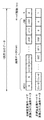
図6は、アナログ入力信号である画素信号とデータメモリ208へ出力される時点でのNビットのデジタルデータであるAD変換出力との関係、つまりADC205の入出力特性を模式的に示す図である。参照電圧Vmは、理想的にはAD変換されて出力コードが4096LSBになるものとする。理想的な入出力特性が得られる場合、点線で示すように入力信号が参照電圧Vmと一致する場合には出力コードは4096LSBとなり、入力信号が参照電圧Vm以上の入出力特性とVm未満の入出力特性は直線状に繋がる。しかし、実際には信号振幅制御部304の記憶容量のばらつきや短絡スイッチの特性などによって、低輝度の場合と高輝度の場合でランプ信号振幅と画素信号振幅の相対関係が想定とずれることがある。この場合には、実線で示すように理想的な入出力特性とずれてしまい、参照電圧Vmを境界に入出力特性に段差や傾きの違いが生じることになる。
FIG. 6 is a diagram schematically showing the relationship between the pixel signal that is an analog input signal and the AD conversion output that is N-bit digital data at the time of output to the
この入出力特性のずれを補正するDFE109のリニアリティ補正部500について、図7を用いて説明する。比較部501は、入力された画像信号の画素データを画素毎に第1の基準値(TH)と比較する。ここでは、第1の基準値THの値は、理想入出力特性において参照電圧Vmのデジタル変換値に相当する4096LSBとする。オフセット補正値選択部502は、比較部501の出力に基づいて、高輝度変換モードのオフセット補正値と低輝度変換モードのオフセット補正値のいずれか一方を選択する。オフセット補正値は、低輝度の場合及び高輝度の場合の各AD変換の入出力特性において、信号振幅制御部304の記憶容量のばらつき等による参照電圧Vmを境界とする入出力特性の段差による理想的な入出力特性からのずれを補正する。補正値の求め方は後述する。
A
比較部501の出力が‘1’の場合、即ち画像信号が第1の基準値TH以上である場合、高輝度変換モードのオフセット補正値が選択される。逆に比較部501の出力が‘0’の場合、即ち画像信号が第1の基準値TH未満である場合、低輝度変換モードのオフセット補正値が選択される。それぞれのオフセット補正値は、撮像素子102の列毎(列毎に配されたADC205毎)に個別の値を設定することができる。つまり、低輝度変換モードのオフセット補正値と高輝度変換モードのオフセット補正値は、それぞれ撮像素子102の列数分のデータとなる。加算部503には、画像信号とオフセット補正値選択部502で選択された補正値が入力され、画像信号に対するオフセット補正が行われる。
When the output of the
また、比較部501の出力はゲイン補正値選択部504にも伝達される。ゲイン補正値は、信号振幅制御部304の記憶容量のばらつき等による入出力特性の傾きを補正するための値である。ゲイン補正値選択部504は、比較部501の出力に基づいて、高輝度変換モードのゲイン補正値と低輝度変換モードのゲイン補正値のいずれか一方を選択する。
The output of the
比較部501の出力が‘1’の場合、即ち画像信号が第1の基準値TH以上である場合、高輝度変換モードのゲイン補正値が選択される。逆に比較部501の出力が‘0’の場合、即ち画像信号が第1の基準値TH未満である場合、低輝度変換モードのゲイン補正値が選択される。それぞれのゲイン補正値は、撮像素子102の列毎(列毎に配されたADC205毎)に個別の値を設定することができる。つまり、低輝度変換モードのゲイン補正値と高輝度変換モードのゲイン補正値は、それぞれ撮像素子102の列数分のデータとなる。乗算部505には、加算部503でオフセット補正が行われた結果の画像信号と、ゲイン補正値選択部504で選択されたゲイン補正値が入力され、画像信号に対するゲイン補正が行われる。乗算部505でゲイン補正された結果は、後段(DSP103)へ出力される。なお、ここでは、オフセット補正値及びゲイン補正値を列毎に個別の値とする構成で説明しているが、列毎のAD変換特性が一致していればこれらの補正値を複数列で共通のものとしてもよい。
When the output of the
また、オフセット補正値及びゲイン補正値は、予め設定しておくことが可能である。この値は、工場での生産工程において取得することも可能である。例えば、図8に示すように、参照電圧Vmより画素信号の信号レベルが低い少なくとも2つの既知の露光条件で基準画像を撮像して、2点からADC205の入出力特性を求めて、低輝度変換モードのオフセット補正値及びゲイン補正値を算出する。同様に、参照電圧Vmより画素信号の信号レベルが高い少なくとも2つの露光条件で撮像した基準画像から高輝度変換モードのオフセット補正値及びゲイン補正値を算出する。なお、図8では、各々2点から補正値を算出するものとして記載しているが、これに限られるものでない。3点以上の条件で画像を取得して、最小二乗法などの手法によってそれぞれの補正値を算出するようにしても構わない。また、補正精度は低下するが、低輝度変換モード・高輝度変換モードで各々1点のみの条件で取得した画像から補正値を算出するようにしても構わない。
The offset correction value and the gain correction value can be set in advance. This value can also be acquired in the production process at the factory. For example, as shown in FIG. 8, a standard image is captured under at least two known exposure conditions in which the signal level of the pixel signal is lower than the reference voltage Vm, and the input / output characteristics of the
以上の構成により、ADC205の入出力特性は理想的な入出力特性に近い形に補正され、補正後の画像としては良好な画質を得ることが可能となる。
With the above configuration, the input / output characteristics of the
[実施形態2]
実施形態1においては第1の基準値THを、参照電圧Vmのデジタル変換値に相当するTH=4096LSBであるものとして説明した。しかし、図6に示すようなAD変換の入出力特性を持つ場合、4096LSB以上の値であるにもかかわらず低輝度変換モードで変換されたデータや、4096LSB未満の値を持つにもかかわらず高輝度変換モードで変換されたデータが出力される可能性がある。このため、実施形態1のようにTH=4096LSBを閾値にして補正する場合、実際には低輝度変換モードで変換された画素データにも関わらず4096LSBを超えているので、高輝度変換モード用の補正値で補正される可能性がある。また、高輝度変換モードで変換された画素データにも関わらず低輝度変換モード用の補正値で補正される可能性がある。このように誤った補正値で補正された場合には、補正分がノイズとなるため第1の基準値TH(4096)付近のレベルで画質が劣化することがある。高画質を求める上ではこうした画質劣化はないのが望ましい。以下、本実施形態を説明するが、実施形態1と重複する部分についての説明は省略する。
[Embodiment 2]
In the first embodiment, the first reference value TH has been described as TH = 4096LSB corresponding to the digital conversion value of the reference voltage Vm. However, when the input / output characteristics of AD conversion as shown in FIG. 6 are used, the data converted in the low luminance conversion mode even though the value is 4096 LSB or higher, or the data is high even though the value is less than 4096 LSB. Data converted in the luminance conversion mode may be output. Therefore, when the correction is performed with TH = 4096LSB as a threshold as in the first embodiment, the pixel data actually exceeds 4096LSB in spite of the pixel data converted in the low luminance conversion mode. There is a possibility of correction with a correction value. Further, there is a possibility that the correction is made with the correction value for the low luminance conversion mode regardless of the pixel data converted in the high luminance conversion mode. When correction is performed with an incorrect correction value in this way, the correction amount becomes noise, and the image quality may deteriorate at a level near the first reference value TH (4096). It is desirable that there is no such deterioration in image quality. Hereinafter, the present embodiment will be described, but the description of the same parts as those in the first embodiment will be omitted.
本実施形態では、図6のように低輝度変換モードと高輝度変換モードの結果に重複部分が発生して同じデジタル値を出力するようなことを避けることにより、全ての画素信号に対して正しい補正が実行されるよう構成する。 In this embodiment, as shown in FIG. 6, it is possible to avoid the occurrence of overlapping portions in the results of the low luminance conversion mode and the high luminance conversion mode and output the same digital value, so that all pixel signals are correct. Configure to perform correction.
図9に本実施形態におけるADC205の入出力特性を示す。低輝度変換モードでVm近傍のレベルを変換した際には、ADC205の出力値は第1の基準値(TH)より低い第2の基準値(THA)以下となるようにAD変換する。また、高輝度変換モードで参照電圧Vm近傍のレベルを変換した際には、ADC205の出力値が第1の基準値THより高い第3の基準値(THB)以上となるようにAD変換を行う。つまり、AD変換モードが違ったときに、ADC205の入出力特性の第1の基準値TH付近において出力値のクロス状態が発生しない部分(以下、ミスコード帯)を設けるようにする。これによって、製造時のばらつきでゲインやオフセットが多少ずれても低輝度変換モードでの変換結果が第1の基準値THを超えないように、また高輝度変換モードでの変換結果が第1の基準値THを下回らないようにすることができる。
FIG. 9 shows the input / output characteristics of the
このようなミスコード帯が存在するような入出力特性は、例えばCDSアンプ203のゲインを下げ、信号振幅制御部304における振幅変更量を小さくする(例えば1/3.8倍など)ことで高輝度モードでの画素信号を大きくして実現できる。信号振幅制御部304の振幅変更量は、第2の記憶容量402の容量値を第3の記憶容量の容量比を変えることによって変更することができる。
The input / output characteristics in which such a miscode band exists can be improved by, for example, lowering the gain of the
特許文献2のように複数のランプ信号を持つ構成の場合は、それぞれのランプ信号の傾きとオフセット(スタート点)を調整することによって、同様に第1の基準値TH付近にミスコード帯を持つ入出力特性を実現することができる。
In the case of a configuration having a plurality of ramp signals as in
以上のように、第1の基準値THを境界に、使用する補正値を切り換えても低輝度と高輝度との間にミスコード帯を設けることにより、変換後の値がクロスしないので、誤った補正を防ぐことができ、良好な画質が実現できる。 As described above, even if the correction value to be used is switched with the first reference value TH as a boundary, by providing a miscode band between the low luminance and the high luminance, the converted value does not cross. Correction can be prevented, and good image quality can be realized.
[実施形態3]
実施形態2において、誤った補正の発生を防ぐ構成について説明した。しかしながら、実施形態2の方法は、入出力特性に図9に示すようなミスコード帯を設けるため、その分のビットが使えないために、信号のダイナミックレンジが僅かながら損なわれる。本実施形態では、オフセット及びゲインの補正を行うDFE109へAD変換モードの情報を伝達することによって、ダイナミックレンジを犠牲にしない方法について説明する。
[Embodiment 3]
In the second embodiment, the configuration for preventing the occurrence of erroneous correction has been described. However, in the method of the second embodiment, the miscode band as shown in FIG. 9 is provided in the input / output characteristics, and the corresponding bits cannot be used, so that the dynamic range of the signal is slightly impaired. In the present embodiment, a method will be described in which dynamic range is not sacrificed by transmitting AD conversion mode information to the
本実施形態におけるADC205の動作について図10により説明する。ADC205は、データメモリ208へNビットの画素データを出力すると共に、FF306の出力を1ビットの情報として、データメモリ208へ出力する。この1ビットの情報は、当該画素が低輝度変換モードと高輝度変換モードのいずれのモードで変換されたかを示すモード情報となる。
The operation of the
本実施形態において撮像素子102から出力される1画素分のデータについて、図11を用いて説明する。撮像素子102からは、画素毎にNビットの画素データと1ビットのモード情報が出力される。DFE109においては、このモード情報に基づいて、各画素のデータに対して補正処理を行う。
Data for one pixel output from the
本実施形態におけるリニアリティ補正を行うDFE109の構成例を図12に示す。DFE109に画素データと共に入力されたモード情報は、オフセット補正値選択部502及びゲイン補正値選択部504の選択信号となる。これによって、各画素のデータは、それぞれの変換モードに応じて誤補正されることなく正しく補正される。ミスコード帯を作る必要がないからダイナミックレンジを有効に使用することが可能となる。
FIG. 12 shows a configuration example of the
[実施形態4]
実施形態3の構成では、撮像素子102からDFE109へ出力するデータが、(N+1)ビット(すなわち画素データNビット+モード情報1ビット)になるため、データ伝送レートは1ビット分だけ高速化する。そこで、本実施形態では、撮像素子102から出力するデータ量を極力小さくし、データ伝送レートを低減する構成について説明する。
[Embodiment 4]
In the configuration of the third embodiment, since the data output from the
本実施形態における撮像素子102の各列のサンプルホールド回路204、ADC205の構成例を図13を用いて説明する。下位ビット置換部312では、ビット拡張部309から出力される画素データの下位1ビットを0に置換する。また、下位ビット置換部313では、ビット拡張部310から出力される画素データの下位1ビットを1に置換する。また、ビット拡張部309,310の出力は、それぞれ比較器316,317にも接続される。比較器316では、画素データと第2の基準値THAを比較し、画素データが第2の基準値THA以上であれば‘1’を、逆に第2の基準値THA未満であれば‘0’を低輝度側データ選択部314に出力する。比較器317では、画素データと第3の基準値THBを比較し、画素データが第3の基準値THB以上であれば‘1’を、逆に第3の基準値THB未満であれば‘0’を高輝度側データ選択部315に出力する。
A configuration example of the
第2の基準値THAは、図14に示すように第1の基準値TH(4096)よりも低いレベル(THA<TH)に設定する。また、第3の基準値THBは、第1の基準値THよりも高いレベル(THB>TH)に設定する。この時、第2の基準値THA未満であれば必ず低輝度変換モードで変換された信号であり、第3の基準値THB以上であれば必ず高輝度変換モードで変換された信号であるように、第2の基準値THAと第3の基準値THBのレベルを設定する。また、第2の基準値THA以上であり第3の基準値THB未満である領域は、ビット拡張部309,310の出力の時点では同じ出力値でも低輝度変換モードで変換されたものと高輝度変換されたものが混在する可能性がある。この領域を以下の説明において便宜上「混在領域」と称することにする。混在領域は図14に示すように入出力特性のクロス状態を含むようにされている。
As shown in FIG. 14, the second reference value THA is set to a level (THA <TH) lower than the first reference value TH (4096). The third reference value THB is set to a level (THB> TH) higher than the first reference value TH. At this time, if it is less than the second reference value THA, it is always a signal converted in the low luminance conversion mode, and if it is greater than or equal to the third reference value THB, it is always a signal converted in the high luminance conversion mode. The levels of the second reference value THA and the third reference value THB are set. Further, an area that is greater than or equal to the second reference value THA and less than the third reference value THB has a high luminance when the same output value is converted in the low luminance conversion mode at the time of output of the
図13に戻り、低輝度側データ選択部314では、比較器316の出力に応じて、ビット拡張部309の出力と下位ビット置換部312の出力のいずれか一方を選択して出力する。同様に、高輝度側データ選択部315では、比較器317の出力に応じて、ビット拡張部310の出力と下位ビット置換部312の出力のいずれか一方を選択して出力する。続く出力データ選択部311では、FF306からの出力に応じて、低輝度側データ選択部314の出力と高輝度側データ選択部315の出力のいずれか一方を選択してデータメモリ208へ出力する。
Returning to FIG. 13, the low luminance side
本実施形態において撮像素子102から出力される1画素分のデータについて、図15を用いて説明する。(1)、(2)は低輝度変換モードで変換された画素のデータ、(3)、(4)は高輝度変換モードで変換された画素のデータである。また、(2)、(3)は混在領域の画素データである。いずれの場合においても、撮像素子102からはNビットのデータが画素毎に出力されるが、混在領域では、最下位の1ビットがモード情報で置き換えられる。DFE109は、このモード情報に基づいて、各画素のデータに対して補正処理を行う。
Data for one pixel output from the
本実施形態におけるリニアリティ補正を行うDFE109について、図16を用いて説明する。比較部511は、画像信号を第3の基準値THBと比較し、画像信号が第3の基準値THB以上であれば‘1’を、第3の基準値THB未満であれば‘0’を出力する。比較部512は、画像信号を第2の基準値THAと比較し、画像信号が第2の基準値THA以上であれば‘1’を、第2の基準値THA未満であれば‘0’を出力する。ANDゲート513の入力には比較部512の出力と画像信号の最下位1ビットとが接続され、その出力はORゲート514の一方の入力に接続されている。ORゲート514の他方の入力には、比較部511の出力が接続されている。これにより、ORゲート514の出力は、画像信号が第3の基準値THB以上である場合か、または画像信号が第2の基準値THA以上、第3の基準値THB未満で画像信号の最下位1ビットが‘1’である場合に‘1’となる。つまり高輝度モードで変換が行われている場合はORゲート514の出力は‘1’になる。低輝度モードで変換が行われると比較部511とANDゲート513の出力は共に‘0’になるので、ORゲート514からは‘0’が出力される。
The
オフセット補正値選択部502及びゲイン補正値選択部504ではORゲート514の出力に応じて、それぞれの補正値を選択する。この例では混在領域においても低輝度変換モードのときは低輝度モードの補正値が選択でき、高輝度変換モードのときは高輝度モードの補正値が選択できる。
The offset correction
以上の構成により、撮像素子102の出力データを増やさずに、ダイナミックレンジも犠牲にしないでかつデータ伝送レートを上げずに各画素のデータを変換モードに応じて正しく補正することができる。なお、本実施形態の構成では画素データの最下位1ビットをモード情報で置き換えるため、混在領域では信号の分解能が1ビット減り、量子化ノイズが増える可能性がある。しかし、混在領域は低輝度変換モードと高輝度変換モードの境界付近であって、比較的光信号成分が多い領域であるため、光ショットノイズが支配的なので、量子化ノイズの画質への影響は少ない。
With the above configuration, the data of each pixel can be correctly corrected according to the conversion mode without increasing the output data of the
[実施形態5]
実施形態3の構成では、撮像素子102からDFE109へ出力するデータが、(N+1)ビット(画素データNビット+モード情報1ビット)となるため、データ伝送レートは高速化する傾向となる。そこで、本実施形態でも、撮像素子102から出力するデータ量を小さくし、データ伝送レートを低減する構成について図17により説明する。ADC205からは、FF306からの1ビットのモード情報と共に、ラッチ回路308に保持された(N−2)ビットのカウント結果がデータメモリ208へそのまま出力される。この結果、撮像素子102からは、図18に示すように(N−2)ビットの画素データ(カウント結果)と、1ビットのモード情報の計(N−1)ビットのデータが画素毎に出力される。DEF109は撮像素子からの(N−1)ビットのデータから(N−2)ビットの画素データと1ビットのモード情報を分離する。(N−2)ビットの画素データにはDFE109において所定数のビットが付加されNビットのデータに拡張される。本実施形態におけるDFE109の主要な構成を図19に示す。拡張部521及び522は、図3のビット拡張部309及び310と同様のビット拡張部であり、それぞれ画像信号入力の上位或いは下位に2ビットの‘0’を付加する。出力データ選択部523は、図3の出力データ選択部311と同様に、モード情報に応じてビット拡張部506,507の出力の一方を選択して加算部503へ画素データを出力する。この時点で、(N−2)ビットの画素データはDFE109において、Nビットに拡張されて出力される。それ以降の処理については、他の実施形態で説明したものと同じであるので、説明を省略する。
[Embodiment 5]
In the configuration of the third embodiment, since the data output from the
以上の構成によれば、撮像素子102から出力するデータ量を画像データ(N−2)ビット+モード情報1ビットの計(N−1)ビットに抑えることができ、データ伝送レートを低減することができる。また、撮像素子102のデータメモリ208からDFE109までの間の回路規模も抑制することができる。
According to the above configuration, the amount of data output from the
更に、本実施形態に、実施形態4に記載したような混在領域の画素データの最下位1ビットをモード情報に置き換える方法を組み合わせて、撮像素子102から出力される1画素あたりのデータを(N−2)ビットに抑制することも可能である。
Further, this embodiment is combined with a method for replacing the least significant 1 bit of the pixel data in the mixed area as described in the fourth embodiment with mode information, and the data per pixel output from the
以上、本発明の実施形態について説明したが、本発明はこれらの実施形態に限定されず、種々の変形及び変更が可能である。 As mentioned above, although embodiment of this invention was described, this invention is not limited to these embodiment, A various deformation | transformation and change are possible.
図8に示すオフセット補正値とゲイン補正値の取得方法では、低輝度変換モードは参照電圧Vm未満の複数点から、高輝度変換モードは参照電圧Vm以上の複数点からそれぞれの補正値を判定して求めるようにしている。しかし、補正値の取得方法はこれに限られるものでなく、例えば図20に示すように各々の変換モードの測定点がそれぞれ参照電圧Vm未満の点と参照電圧Vm以上の点を含むようにしてもよい。その場合にはより幅広い信号範囲から補正値を判定することができるため各測定点の測定誤差の影響を受けにくく、補正値算出精度の向上が期待できる。場合によっては、高輝度変換モード/低輝度変換モードのいずか一方のみが、測定点に参照電圧Vm未満のレベルと参照電圧Vm以上のレベルを含むようにしても構わない。 In the method of acquiring the offset correction value and the gain correction value shown in FIG. 8, the correction value is determined from a plurality of points less than the reference voltage Vm in the low luminance conversion mode and from a plurality of points higher than the reference voltage Vm in the high luminance conversion mode. To ask. However, the method of acquiring the correction value is not limited to this, and for example, as shown in FIG. 20, the measurement points in each conversion mode may include points that are less than the reference voltage Vm and points that are greater than or equal to the reference voltage Vm. . In this case, since the correction value can be determined from a wider signal range, it is difficult to be affected by the measurement error at each measurement point, and improvement in correction value calculation accuracy can be expected. In some cases, only one of the high luminance conversion mode and the low luminance conversion mode may include a level lower than the reference voltage Vm and a level higher than the reference voltage Vm at the measurement point.
また、モード毎の測定誤差軽減のため、図21に示すように各々のモードの測定に同じアナログ入力電圧を使うようにしてもよい。この場合、モード毎に測定に使う電圧が異なることによって発生する誤差を抑制することが可能である。 In order to reduce the measurement error for each mode, the same analog input voltage may be used for measurement in each mode as shown in FIG. In this case, it is possible to suppress errors that occur due to different voltages used for measurement in each mode.
また、オフセット補正値やゲイン補正値の取得は、撮像装置の電源起動時や実際の撮像時の撮像操作に応じて行うようにすることも可能である。その場合には、補正値取得のために撮像素子102の画素201以降の何処かに画素信号の代わりに測定用の擬似信号レベルを入力してAD変換の入出力特性を測定して行う。
Further, the offset correction value and the gain correction value can be acquired according to the imaging operation at the time of power activation of the imaging apparatus or actual imaging. In that case, in order to obtain a correction value, a pseudo signal level for measurement is input in place of the pixel signal somewhere after the
上述の実施形態では、画素信号の振幅を変更することにより低輝度変換モードと高輝度変換モードを切り換える場合のAD変換時の入出力特性の補正について説明した。しかし、特許文献2のようにランプ信号の傾きを変更することにより変換モードの切替えを行う構成に対しても、補正値を測定して求めることにより本実施形態に例示するようにAD変換の入出力特性の補正を行うことが可能である。
In the above-described embodiment, the correction of input / output characteristics at the time of AD conversion when switching between the low luminance conversion mode and the high luminance conversion mode by changing the amplitude of the pixel signal has been described. However, even in the configuration in which the conversion mode is switched by changing the slope of the ramp signal as in
また、上述の実施形態では最終的なデジタルデータの出力値をN=14ビットとして説明しているが、これに限られるものではなく、システムに応じて好適なビット数で構成して構わない。カウンタのビット幅や参照電圧についてもAD変換速度や量子化誤差を考慮した好適なビット数や電圧により構成して構わない。 In the above-described embodiment, the output value of the final digital data is described as N = 14 bits. However, the present invention is not limited to this, and may be configured with a suitable number of bits according to the system. The bit width and reference voltage of the counter may be configured with a suitable number of bits and voltage in consideration of AD conversion speed and quantization error.
上述の実施形態では、ビット拡張部において上位或いは下位に‘0’を付加してビット拡張を行う構成としたが、ビットの拡張方法はこれに限られるものではない。下位に付加するビットについては‘0’だけでなく‘1’が含まれていても構わない。また、ランダムなデータを発生する回路をビット拡張部に配し、下位にはこのランダムデータを付加するようにしても構わない。また、ビット拡張部の構成を上位或いは下位にビットを付加する構成としているが、乗算器で構成しても構わない。例えば、閾値Vmをフルスケール振幅の1/3とした場合、画素信号が閾値Vm以上である場合には振幅制御部で振幅を1/3にし、ビット拡張部に乗算器を設けて3倍を掛けるようにすることもできる。 In the above-described embodiment, the bit expansion unit is configured to perform bit expansion by adding “0” to the upper or lower order, but the bit expansion method is not limited to this. For the bits added to the lower order, not only “0” but also “1” may be included. Further, a circuit that generates random data may be arranged in the bit extension unit, and the random data may be added to the lower order. In addition, although the bit extension unit is configured to add bits to the upper or lower order, it may be configured by a multiplier. For example, when the threshold value Vm is set to 1/3 of the full-scale amplitude, when the pixel signal is equal to or greater than the threshold value Vm, the amplitude control unit sets the amplitude to 1/3, and a bit extension unit is provided with a multiplier to increase 3 times. It can also be hung.
Claims (11)
前記画素からの画素信号と参照電圧とを比較する比較手段と、
前記比較手段による比較の結果、
前記画素信号が前記参照電圧未満である場合に前記画素信号を低輝度変換モードでアナログ−デジタル(AD)変換し、前記画素信号が前記参照電圧以上である場合に前記画素信号を高輝度変換モードでAD変換するAD変換手段と、
前記AD変換手段の出力データに対して、前記AD変換により生じるオフセットおよびゲインを補正する補正手段と、を備え、
前記補正手段は、前記AD変換手段が前記画素信号を前記低輝度変換モードでAD変換する場合に前記低輝度変換モード用のオフセット補正値およびゲイン補正値を用いて前記AD変換手段の出力データのオフセットおよびゲインを補正し、前記AD変換手段が前記画素信号を前記高輝度変換モードでAD変換する場合に前記高輝度変換モード用のオフセット補正値およびゲイン補正値を用いて前記AD変換手段の出力データのオフセットおよびゲインを補正することを特徴とする撮像装置。 A pixel that converts light into an electrical signal;
Comparing means for comparing a pixel signal from the pixel with a reference voltage;
As a result of comparison by the comparison means ,
When the pixel signal is less than the reference voltage, the pixel signal is analog-digital (AD) converted in a low luminance conversion mode, and when the pixel signal is equal to or higher than the reference voltage, the pixel signal is converted into a high luminance conversion mode. an AD converter for AD converting in,
The output data of the AD converter, Bei example and a correcting means for correcting the offset and gain caused by the AD conversion,
The correction means uses the offset correction value and gain correction value for the low luminance conversion mode when the AD conversion means AD converts the pixel signal in the low luminance conversion mode . The offset and gain are corrected, and when the AD converter performs AD conversion on the pixel signal in the high luminance conversion mode, the output of the AD converter using the offset correction value and gain correction value for the high luminance conversion mode An image pickup apparatus that corrects offset and gain of data .
前記ビット拡張手段は、前記AD変換手段の出力データの上位又は下位にビットを付加して前記AD変換手段の出力データのビット数を前記所定数に拡張することを特徴とする請求項1乃至4のいずれか1項に記載の撮像装置。 Bit extension means for extending the number of bits of output data of the AD conversion means to a predetermined number;
5. The bit extension means adds a bit to the upper or lower order of the output data of the AD conversion means to extend the number of bits of the output data of the AD conversion means to the predetermined number. The imaging device according to any one of the above.
Priority Applications (2)
| Application Number | Priority Date | Filing Date | Title |
|---|---|---|---|
| JP2013098892A JP6226551B2 (en) | 2013-05-08 | 2013-05-08 | Imaging device |
| US14/262,212 US9848150B2 (en) | 2013-05-08 | 2014-04-25 | Image pickup apparatus comprising A/D converter with offset and gain correction based on amplitude of input signal |
Applications Claiming Priority (1)
| Application Number | Priority Date | Filing Date | Title |
|---|---|---|---|
| JP2013098892A JP6226551B2 (en) | 2013-05-08 | 2013-05-08 | Imaging device |
Publications (3)
| Publication Number | Publication Date |
|---|---|
| JP2014220663A JP2014220663A (en) | 2014-11-20 |
| JP2014220663A5 JP2014220663A5 (en) | 2016-06-16 |
| JP6226551B2 true JP6226551B2 (en) | 2017-11-08 |
Family
ID=51864529
Family Applications (1)
| Application Number | Title | Priority Date | Filing Date |
|---|---|---|---|
| JP2013098892A Active JP6226551B2 (en) | 2013-05-08 | 2013-05-08 | Imaging device |
Country Status (2)
| Country | Link |
|---|---|
| US (1) | US9848150B2 (en) |
| JP (1) | JP6226551B2 (en) |
Families Citing this family (13)
| Publication number | Priority date | Publication date | Assignee | Title |
|---|---|---|---|---|
| JP6433276B2 (en) * | 2014-12-09 | 2018-12-05 | キヤノン株式会社 | Imaging apparatus, control method therefor, program, and storage medium |
| CN104618701B (en) | 2015-01-13 | 2017-03-29 | 小米科技有限责任公司 | Image processing method and device, electronic equipment |
| JP6494301B2 (en) * | 2015-01-22 | 2019-04-03 | キヤノン株式会社 | Imaging apparatus and control method thereof |
| JP6525602B2 (en) * | 2015-01-22 | 2019-06-05 | キヤノン株式会社 | Image pickup apparatus and control method thereof |
| CN104732938B (en) * | 2015-03-27 | 2017-05-17 | 深圳市华星光电技术有限公司 | Drive method and drive device of liquid crystal display panel |
| WO2016158315A1 (en) * | 2015-03-27 | 2016-10-06 | ソニー株式会社 | Imaging element, imaging method, and electronic device |
| KR101815896B1 (en) * | 2015-05-29 | 2018-01-09 | 엘지디스플레이 주식회사 | Timing controller and display device |
| US9838637B2 (en) * | 2015-10-21 | 2017-12-05 | Canon Kabushiki Kaisha | Solid-state image sensor, method of controlling the same, image sensing system, and camera |
| KR102384463B1 (en) * | 2015-10-30 | 2022-04-07 | 삼성전자주식회사 | Data transfer circuit using digital transfer and image sensor including same |
| JP6985827B2 (en) * | 2016-10-04 | 2021-12-22 | キヤノン株式会社 | Imaging device, its driving method and imaging system |
| US11424115B2 (en) * | 2017-03-31 | 2022-08-23 | Verity Instruments, Inc. | Multimode configurable spectrometer |
| JP2019002760A (en) * | 2017-06-14 | 2019-01-10 | オムロンオートモーティブエレクトロニクス株式会社 | Distance measuring device |
| JP2021063976A (en) | 2019-10-16 | 2021-04-22 | キヤノン株式会社 | Focus detector and method for controlling the same, program, and storage medium |
Family Cites Families (24)
| Publication number | Priority date | Publication date | Assignee | Title |
|---|---|---|---|---|
| JPH0548460A (en) | 1991-06-05 | 1993-02-26 | Matsushita Electric Ind Co Ltd | A/d converter and sensor using the same and three-dimensional integrated circuit |
| US6353401B1 (en) * | 1998-06-15 | 2002-03-05 | Texas Instruments Incorporated | Optical sensor array with zone-programmable gain and offset |
| US7903159B2 (en) * | 2001-03-26 | 2011-03-08 | Panavision Imaging Llc | Image sensor ADC and CDS per column |
| US7508421B2 (en) * | 2002-06-24 | 2009-03-24 | Fujifilm Corporation | Image pickup apparatus and image processing method |
| US7038720B2 (en) * | 2002-10-16 | 2006-05-02 | Exar Corporation | Pixel-by-pixel digital control of gain and offset correction for video imaging |
| JP4219341B2 (en) * | 2004-06-01 | 2009-02-04 | 三洋電機株式会社 | Analog-digital converter, signal processing system using the same, and imaging apparatus |
| JP4654857B2 (en) * | 2005-09-26 | 2011-03-23 | ソニー株式会社 | DA converter, AD converter, semiconductor device |
| JP4882652B2 (en) * | 2006-10-06 | 2012-02-22 | ソニー株式会社 | Solid-state imaging device, driving method of solid-state imaging device, and imaging device |
| JP4609428B2 (en) * | 2006-12-27 | 2011-01-12 | ソニー株式会社 | Solid-state imaging device, driving method of solid-state imaging device, and imaging device |
| US7671317B2 (en) * | 2007-07-25 | 2010-03-02 | Panasonic Corporation | Physical quantity detecting apparatus and method for driving the same |
| JP4389981B2 (en) * | 2007-08-06 | 2009-12-24 | ソニー株式会社 | Solid-state imaging device, analog-digital conversion method of solid-state imaging device, and imaging device |
| TWI399088B (en) * | 2007-10-12 | 2013-06-11 | Sony Corp | Data processor, solid-state imaging device, imaging device, and electronic apparatus |
| JP2009159069A (en) * | 2007-12-25 | 2009-07-16 | Panasonic Corp | Solid-state imaging device and camera |
| JP2009177749A (en) * | 2008-01-28 | 2009-08-06 | Panasonic Corp | Solid-state imaging apparatus |
| FR2935076A1 (en) | 2008-08-18 | 2010-02-19 | St Microelectronics Sa | ANALOG-DIGITAL CONVERTER |
| JP2010074331A (en) | 2008-09-17 | 2010-04-02 | Riniaseru Design:Kk | Solid-state imaging apparatus |
| JP2011234154A (en) * | 2010-04-28 | 2011-11-17 | Renesas Electronics Corp | Analog-to-digital converter and operation method thereof |
| JP2011250039A (en) * | 2010-05-25 | 2011-12-08 | Panasonic Corp | Solid-state imaging device, semiconductor integrated circuit device, camera, and signal processing method |
| JP5645505B2 (en) * | 2010-06-29 | 2014-12-24 | キヤノン株式会社 | Imaging apparatus and control method thereof |
| JP5528282B2 (en) * | 2010-09-30 | 2014-06-25 | キヤノン株式会社 | Solid-state imaging device |
| KR20120064503A (en) * | 2010-12-09 | 2012-06-19 | 한국전자통신연구원 | Pipelined analog digital convertor |
| US8648913B2 (en) * | 2011-04-15 | 2014-02-11 | Omnivision Technologies, Inc. | Missing code redistribution in pipeline analog to digital converter |
| JP5871531B2 (en) * | 2011-09-08 | 2016-03-01 | キヤノン株式会社 | Imaging apparatus and imaging system |
| EP2696506A1 (en) * | 2012-08-09 | 2014-02-12 | Innovaciones Microelectronicas S.L. | Two-stage analog-to-digital converter for high-speed image sensor |
-
2013
- 2013-05-08 JP JP2013098892A patent/JP6226551B2/en active Active
-
2014
- 2014-04-25 US US14/262,212 patent/US9848150B2/en active Active
Also Published As
| Publication number | Publication date |
|---|---|
| JP2014220663A (en) | 2014-11-20 |
| US9848150B2 (en) | 2017-12-19 |
| US20140333816A1 (en) | 2014-11-13 |
Similar Documents
| Publication | Publication Date | Title |
|---|---|---|
| JP6226551B2 (en) | Imaging device | |
| US10116320B2 (en) | Photoelectric conversion apparatus and image capturing system | |
| CN109640010B (en) | Electronic device and image capturing method | |
| US8264580B2 (en) | Solid state imaging device, signal processing method of solid-state imaging device and imaging apparatus capable of removing vertical smears | |
| JP4449565B2 (en) | Semiconductor device for physical quantity distribution detection | |
| TWI404411B (en) | Solid-state imaging device, control method therefor, and camera system | |
| TWI535291B (en) | Signal processing device and signal processing method | |
| JP5094498B2 (en) | Solid-state imaging device and imaging system | |
| EP2104235B1 (en) | Analog-to-digital converter, analog-to-digital converting method, solid-state image pickup device. | |
| US8606051B2 (en) | Frame-wise calibration of column-parallel ADCs for image sensor array applications | |
| JP2011211535A (en) | Solid-state imaging device and camera system | |
| US9071778B2 (en) | Ad converting circuit, photoelectric converting apparatus, image pickup system, and driving method for ad converting circuit | |
| CN107154803B (en) | Signal processing apparatus, signal processing method, and image pickup apparatus | |
| US20140168449A1 (en) | Image pickup apparatus, image pickup system, and method for driving image pickup apparatus | |
| JP6486001B2 (en) | AD converter, AD conversion apparatus, photoelectric conversion apparatus, imaging system, and AD conversion method | |
| JP2016048813A (en) | Solid-state imaging device, imaging method and electronic apparatus | |
| US8963758B2 (en) | Image sensor and image capturing apparatus | |
| JP2012034217A (en) | Solid state image pickup device | |
| US20100110231A1 (en) | Output control circuit and imaging device | |
| JP6112871B2 (en) | Imaging device and imaging apparatus | |
| JP4340803B2 (en) | System and method for correcting erroneous image signals from defective photosensitive pixels | |
| JP2006128752A (en) | A/d conversion method, a/d converter, method and device for acquiring physical information | |
| JP6433276B2 (en) | Imaging apparatus, control method therefor, program, and storage medium | |
| US11284017B2 (en) | Image pickup device and storage medium | |
| JP6824678B2 (en) | Image sensor, image sensor, and signal processing method for image sensor |
Legal Events
| Date | Code | Title | Description |
|---|---|---|---|
| A521 | Request for written amendment filed |
Free format text: JAPANESE INTERMEDIATE CODE: A523 Effective date: 20160422 |
|
| A621 | Written request for application examination |
Free format text: JAPANESE INTERMEDIATE CODE: A621 Effective date: 20160422 |
|
| A977 | Report on retrieval |
Free format text: JAPANESE INTERMEDIATE CODE: A971007 Effective date: 20170119 |
|
| A131 | Notification of reasons for refusal |
Free format text: JAPANESE INTERMEDIATE CODE: A131 Effective date: 20170213 |
|
| A521 | Request for written amendment filed |
Free format text: JAPANESE INTERMEDIATE CODE: A523 Effective date: 20170411 |
|
| TRDD | Decision of grant or rejection written | ||
| A01 | Written decision to grant a patent or to grant a registration (utility model) |
Free format text: JAPANESE INTERMEDIATE CODE: A01 Effective date: 20170911 |
|
| A61 | First payment of annual fees (during grant procedure) |
Free format text: JAPANESE INTERMEDIATE CODE: A61 Effective date: 20171010 |
|
| R151 | Written notification of patent or utility model registration |
Ref document number: 6226551 Country of ref document: JP Free format text: JAPANESE INTERMEDIATE CODE: R151 |