JP6219656B2 - Organic EL display device - Google Patents
Organic EL display device Download PDFInfo
- Publication number
- JP6219656B2 JP6219656B2 JP2013202935A JP2013202935A JP6219656B2 JP 6219656 B2 JP6219656 B2 JP 6219656B2 JP 2013202935 A JP2013202935 A JP 2013202935A JP 2013202935 A JP2013202935 A JP 2013202935A JP 6219656 B2 JP6219656 B2 JP 6219656B2
- Authority
- JP
- Japan
- Prior art keywords
- pixels
- pixel
- hole
- organic
- lower electrode
- Prior art date
- Legal status (The legal status is an assumption and is not a legal conclusion. Google has not performed a legal analysis and makes no representation as to the accuracy of the status listed.)
- Active
Links
- 239000000758 substrate Substances 0.000 claims description 30
- 238000005192 partition Methods 0.000 claims description 11
- 230000000149 penetrating effect Effects 0.000 claims 1
- 238000005401 electroluminescence Methods 0.000 description 40
- 239000010410 layer Substances 0.000 description 40
- 230000001788 irregular Effects 0.000 description 29
- 239000010408 film Substances 0.000 description 21
- 239000011368 organic material Substances 0.000 description 18
- 238000000034 method Methods 0.000 description 12
- 239000004020 conductor Substances 0.000 description 9
- 239000011521 glass Substances 0.000 description 6
- 239000011159 matrix material Substances 0.000 description 5
- 238000007789 sealing Methods 0.000 description 5
- 230000007423 decrease Effects 0.000 description 4
- 238000010586 diagram Methods 0.000 description 4
- 230000006870 function Effects 0.000 description 4
- 230000015572 biosynthetic process Effects 0.000 description 3
- 239000003990 capacitor Substances 0.000 description 3
- 239000003086 colorant Substances 0.000 description 3
- 238000010030 laminating Methods 0.000 description 3
- 239000000463 material Substances 0.000 description 3
- 239000012044 organic layer Substances 0.000 description 3
- 238000002834 transmittance Methods 0.000 description 3
- 230000006866 deterioration Effects 0.000 description 2
- AMGQUBHHOARCQH-UHFFFAOYSA-N indium;oxotin Chemical compound [In].[Sn]=O AMGQUBHHOARCQH-UHFFFAOYSA-N 0.000 description 2
- 229910052751 metal Inorganic materials 0.000 description 2
- 239000002184 metal Substances 0.000 description 2
- 239000000203 mixture Substances 0.000 description 2
- YVTHLONGBIQYBO-UHFFFAOYSA-N zinc indium(3+) oxygen(2-) Chemical compound [O--].[Zn++].[In+3] YVTHLONGBIQYBO-UHFFFAOYSA-N 0.000 description 2
- 229910001111 Fine metal Inorganic materials 0.000 description 1
- BQCADISMDOOEFD-UHFFFAOYSA-N Silver Chemical compound [Ag] BQCADISMDOOEFD-UHFFFAOYSA-N 0.000 description 1
- 229910052782 aluminium Inorganic materials 0.000 description 1
- XAGFODPZIPBFFR-UHFFFAOYSA-N aluminium Chemical compound [Al] XAGFODPZIPBFFR-UHFFFAOYSA-N 0.000 description 1
- 230000005540 biological transmission Effects 0.000 description 1
- 230000000903 blocking effect Effects 0.000 description 1
- 238000006243 chemical reaction Methods 0.000 description 1
- 230000000694 effects Effects 0.000 description 1
- 239000007772 electrode material Substances 0.000 description 1
- 230000005525 hole transport Effects 0.000 description 1
- 230000001678 irradiating effect Effects 0.000 description 1
- 238000004519 manufacturing process Methods 0.000 description 1
- 238000000206 photolithography Methods 0.000 description 1
- 229910052709 silver Inorganic materials 0.000 description 1
- 239000004332 silver Substances 0.000 description 1
- 238000000638 solvent extraction Methods 0.000 description 1
- 239000010409 thin film Substances 0.000 description 1
- 238000007740 vapor deposition Methods 0.000 description 1
Images


Classifications
-
- H—ELECTRICITY
- H10—SEMICONDUCTOR DEVICES; ELECTRIC SOLID-STATE DEVICES NOT OTHERWISE PROVIDED FOR
- H10K—ORGANIC ELECTRIC SOLID-STATE DEVICES
- H10K59/00—Integrated devices, or assemblies of multiple devices, comprising at least one organic light-emitting element covered by group H10K50/00
- H10K59/30—Devices specially adapted for multicolour light emission
- H10K59/35—Devices specially adapted for multicolour light emission comprising red-green-blue [RGB] subpixels
- H10K59/351—Devices specially adapted for multicolour light emission comprising red-green-blue [RGB] subpixels comprising more than three subpixels, e.g. red-green-blue-white [RGBW]
-
- H—ELECTRICITY
- H10—SEMICONDUCTOR DEVICES; ELECTRIC SOLID-STATE DEVICES NOT OTHERWISE PROVIDED FOR
- H10K—ORGANIC ELECTRIC SOLID-STATE DEVICES
- H10K50/00—Organic light-emitting devices
- H10K50/80—Constructional details
- H10K50/805—Electrodes
- H10K50/82—Cathodes
- H10K50/824—Cathodes combined with auxiliary electrodes
-
- H—ELECTRICITY
- H10—SEMICONDUCTOR DEVICES; ELECTRIC SOLID-STATE DEVICES NOT OTHERWISE PROVIDED FOR
- H10K—ORGANIC ELECTRIC SOLID-STATE DEVICES
- H10K59/00—Integrated devices, or assemblies of multiple devices, comprising at least one organic light-emitting element covered by group H10K50/00
- H10K59/10—OLED displays
- H10K59/12—Active-matrix OLED [AMOLED] displays
- H10K59/121—Active-matrix OLED [AMOLED] displays characterised by the geometry or disposition of pixel elements
- H10K59/1216—Active-matrix OLED [AMOLED] displays characterised by the geometry or disposition of pixel elements the pixel elements being capacitors
-
- H—ELECTRICITY
- H10—SEMICONDUCTOR DEVICES; ELECTRIC SOLID-STATE DEVICES NOT OTHERWISE PROVIDED FOR
- H10K—ORGANIC ELECTRIC SOLID-STATE DEVICES
- H10K59/00—Integrated devices, or assemblies of multiple devices, comprising at least one organic light-emitting element covered by group H10K50/00
- H10K59/10—OLED displays
- H10K59/12—Active-matrix OLED [AMOLED] displays
- H10K59/122—Pixel-defining structures or layers, e.g. banks
-
- H—ELECTRICITY
- H10—SEMICONDUCTOR DEVICES; ELECTRIC SOLID-STATE DEVICES NOT OTHERWISE PROVIDED FOR
- H10K—ORGANIC ELECTRIC SOLID-STATE DEVICES
- H10K59/00—Integrated devices, or assemblies of multiple devices, comprising at least one organic light-emitting element covered by group H10K50/00
- H10K59/10—OLED displays
- H10K59/12—Active-matrix OLED [AMOLED] displays
- H10K59/123—Connection of the pixel electrodes to the thin film transistors [TFT]
-
- H—ELECTRICITY
- H10—SEMICONDUCTOR DEVICES; ELECTRIC SOLID-STATE DEVICES NOT OTHERWISE PROVIDED FOR
- H10K—ORGANIC ELECTRIC SOLID-STATE DEVICES
- H10K59/00—Integrated devices, or assemblies of multiple devices, comprising at least one organic light-emitting element covered by group H10K50/00
- H10K59/10—OLED displays
- H10K59/12—Active-matrix OLED [AMOLED] displays
- H10K59/131—Interconnections, e.g. wiring lines or terminals
-
- H—ELECTRICITY
- H10—SEMICONDUCTOR DEVICES; ELECTRIC SOLID-STATE DEVICES NOT OTHERWISE PROVIDED FOR
- H10K—ORGANIC ELECTRIC SOLID-STATE DEVICES
- H10K59/00—Integrated devices, or assemblies of multiple devices, comprising at least one organic light-emitting element covered by group H10K50/00
- H10K59/30—Devices specially adapted for multicolour light emission
- H10K59/38—Devices specially adapted for multicolour light emission comprising colour filters or colour changing media [CCM]
-
- H—ELECTRICITY
- H10—SEMICONDUCTOR DEVICES; ELECTRIC SOLID-STATE DEVICES NOT OTHERWISE PROVIDED FOR
- H10K—ORGANIC ELECTRIC SOLID-STATE DEVICES
- H10K59/00—Integrated devices, or assemblies of multiple devices, comprising at least one organic light-emitting element covered by group H10K50/00
- H10K59/80—Constructional details
- H10K59/805—Electrodes
- H10K59/8052—Cathodes
- H10K59/80522—Cathodes combined with auxiliary electrodes
-
- H—ELECTRICITY
- H10—SEMICONDUCTOR DEVICES; ELECTRIC SOLID-STATE DEVICES NOT OTHERWISE PROVIDED FOR
- H10K—ORGANIC ELECTRIC SOLID-STATE DEVICES
- H10K2102/00—Constructional details relating to the organic devices covered by this subclass
- H10K2102/301—Details of OLEDs
- H10K2102/302—Details of OLEDs of OLED structures
- H10K2102/3023—Direction of light emission
- H10K2102/3026—Top emission
Landscapes
- Engineering & Computer Science (AREA)
- Microelectronics & Electronic Packaging (AREA)
- Physics & Mathematics (AREA)
- Optics & Photonics (AREA)
- Geometry (AREA)
- Electroluminescent Light Sources (AREA)
- Devices For Indicating Variable Information By Combining Individual Elements (AREA)
Description
本発明は有機エレクトロルミネッセンス(electroluminescence:EL)表示装置に関し、特に有機発光素子の電極のうち表示領域に配列された複数画素に共通に形成される電極における電位の均一化に関する。 The present invention relates to an organic electroluminescence (EL) display device, and more particularly to equalization of potentials of electrodes formed in common among a plurality of pixels arranged in a display region among electrodes of an organic light emitting element.
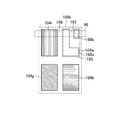
有機EL表示装置はTFT基板と対向基板とを貼り合わせた構造を有する。図7は従来の有機EL表示装置2のTFT基板4の表示領域の模式的な部分断面図であり、表示領域の水平方向に沿った垂直断面を示している。TFT基板4は例えば、ガラス基板6上に回路層8、絶縁膜10、バンク12、有機発光ダイオード(Organic Light-Emitting Diode:OLED)14及び封止膜16などを積層される。
The organic EL display device has a structure in which a TFT substrate and a counter substrate are bonded together. FIG. 7 is a schematic partial cross-sectional view of the display area of the TFT substrate 4 of the conventional organic
表示領域には複数の画素が二次元配列される。カラー表示を行う有機EL表示装置では、各画素は互いに異なる色で発光する複数のサブピクセルからなる。例えば、画素は赤色(R)で発光するRサブピクセル、緑色(G)で発光するGサブピクセル、青色(B)で発光するBサブピクセルで構成することができ、またこれらに白色(W)で発光するWサブピクセルを加えた4サブピクセルで1画素を構成することも行われる。 A plurality of pixels are two-dimensionally arranged in the display area. In an organic EL display device that performs color display, each pixel includes a plurality of sub-pixels that emit light of different colors. For example, the pixel may be composed of an R sub-pixel emitting red (R), a G sub-pixel emitting green (G), and a B sub-pixel emitting blue (B), and white (W). One pixel is also formed by four subpixels including the W subpixel that emits light.
OLED14はサブピクセルごとにバンク12(隔壁)で囲まれた開口領域に形成され、下部電極20、有機層22(有機材料層)及び上部電極24を含んで構成される。下部電極20及び上部電極24はそれぞれOLEDのアノード電極(陽極)、カソード電極(陰極)を構成し、これらの間に印加される電気信号により有機層22での発光が制御される。上部電極24は基本的に表示領域全体の画素に共通に形成され、表示領域の縁にて給電線に接続され駆動部から共通電圧を印加される。一方、下部電極20は画素ごとに形成され、回路層8に形成される各画素の画素回路及び駆動電源線を介して駆動部から映像信号に応じた電流を供給される。
The OLED 14 is formed in an opening region surrounded by the bank 12 (partition wall) for each subpixel, and includes a
バンク12はOLED、特に有機層22をサブピクセルごとに区切って形成するための隔壁としての機能を有する。またバンク12は絶縁層で形成され、開口領域ごとに形成される下部電極20間の短絡を防止する。
The
上部電極24及び下部電極20は例えば、IZO(Indium Zinc Oxide)やITO(Indium Tin Oxide)等の透明導電材を用いて形成される。特に、トップエミッション型の有機EL表示装置では、消費電力低減の観点から上部電極24の光の透過率は高いことが望ましい。ここで、透明電導電材を薄くすれば上部電極24の透過率は上がるが、その反面、上部電極24の導電率が低下し、OLEDに流れる電流に起因する電圧降下が大きくなる。具体的には上部電極24において給電線に近い位置と遠い位置とでの電位差が大きくなる。その結果、給電線から遠い位置ほどOLEDの電流密度が低下して輝度が低下するシェーディング(輝度傾斜)が生じる。すなわち、発光輝度が表示領域内で一様でなくなり表示むらを生じるという問題がある。この問題は表示パネルが大面積化するほど顕著となる。
The
そこで、抵抗値の低い材料を用いて導通を補助する給電配線を形成し、バンク12に形成したコンタクトホールを介して上部電極24と給電配線とを接続することで、上部電極24の実質的な低抵抗化を図ることが提案されている(特許文献1)。
Therefore, a power supply wiring that assists conduction is formed using a material having a low resistance value, and the
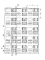
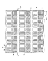
図8、図9は上部電極24と給電配線30とを接続するコンタクトホール32をバンク12に形成した有機EL表示装置の表示領域の一部分の平面図である。ここでは各画素34がRGBWの4つのサブピクセル36からなる例を示している。図8は水平方向に隣接する画素34の間のバンク12にコンタクトホール32を配置する場合を示しており、図9は垂直方向に隣接する画素34の間のバンク12にコンタクトホール32を配置する場合を示している。
8 and 9 are plan views of a part of the display region of the organic EL display device in which the
図8、図9に示すようにコンタクトホール32を配置するバンク12は、コンタクトホール32を配置しない場合のバンクより大きな幅を要する部分を生じる。すなわち、上部電極24と給電配線30とを接続するコンタクトホール32をバンク12に形成する構成では、バンク12の幅はバンク12の本来の機能から必要とされる以上のサイズとなりバンク12の微細化が制限されるので、有機EL表示装置の高精細化に不利であるという問題があった。
As shown in FIGS. 8 and 9, the
また、図8、図9に示すように、コンタクトホール32は上部電極24の導電率によっては必ずしも画素ごとに設けなくてもよい。しかし、画像表示装置では表示品質確保のため画素の配列ピッチを表示領域内にて一様にするので、電気特性上、コンタクトホール32を配置する必要がない位置のバンク12の幅、面積がコンタクトホール32を設ける位置のバンク12と同様に大きく形成され、無駄な非発光領域が大きくなる。
Further, as shown in FIGS. 8 and 9, the
具体的には、図8、図9に示すマトリクス状の画素配列にて水平方向の画素ピッチをx、垂直方向の画素ピッチをyとすると、図8に示す構成では、バンク12にコンタクトホール32を配置しない場合よりもxが大きくなり、図9に示す構成では、バンク12にコンタクトホール32を配置しない場合よりもyが大きくなる。画素ピッチの増加は高精細化に不利であることを意味し、また当該増加はバンク12の幅の増加によるものであり、非発光領域の増加を意味する。
Specifically, in the matrix pixel arrangement shown in FIGS. 8 and 9, assuming that the horizontal pixel pitch is x and the vertical pixel pitch is y, in the configuration shown in FIG. 9 is larger than when no
本発明は上記問題点を解決するためになされたものであり、画素の開口率を高く維持しつつ、シェーディングを抑制し高品位の画質が得られる有機EL表示装置を提供することを目的とする。 The present invention has been made to solve the above-described problems, and an object thereof is to provide an organic EL display device capable of suppressing shading and obtaining high-quality image quality while maintaining a high aperture ratio of pixels. .
(1)本発明に係る有機EL表示装置は、隔壁で囲まれた開口領域に形成された有機発光素子を少なくとも1つ含み共通の形を有する複数の画素を二次元配列され、基板の上に形成され前記有機発光素子の駆動の基準電位を供給される給電配線を有し、前記有機発光素子は、前記給電配線が形成された前記基板の上に形成され、下から順に下部電極、有機材料層、及び前記複数の画素に共通の上部電極が積層された構造を有し、前記複数の画素のうちの一部の画素は、前記有機材料層を貫通して前記上部電極と前記給電配線とを電気的に接続する垂直配線を前記開口領域内に形成された変則画素であるものである。 (1) In the organic EL display device according to the present invention, a plurality of pixels having at least one organic light emitting element formed in an opening region surrounded by a partition and having a common shape are two-dimensionally arranged on a substrate. A power supply wiring that is formed and supplied with a reference potential for driving the organic light emitting element, and the organic light emitting element is formed on the substrate on which the power supply wiring is formed, and a lower electrode and an organic material are sequentially formed from the bottom. And an upper electrode common to the plurality of pixels is laminated, and some of the plurality of pixels pass through the organic material layer and include the upper electrode and the power supply wiring. Are vertical pixels that are electrically connected to each other and are irregular pixels formed in the opening region.
(2)上記(1)に記載する有機EL表示装置において、前記画素は、赤色、緑色、青色及び白色で発光する4つの前記開口領域を含み、前記変則画素は、白色発光の前記開口領域の全部又は一部に、前記有機発光素子の構造に代えて前記垂直配線を形成される構成とすることができる。 (2) In the organic EL display device according to (1), the pixel includes four opening regions that emit light in red, green, blue, and white, and the irregular pixel includes the opening region that emits white light. The vertical wiring may be formed in whole or in part in place of the structure of the organic light emitting device.
(3)上記(1)に記載する有機EL表示装置において、前記画素は赤色、緑色及び青色で発光する3つの前記開口領域からなり、前記変則画素は、青色発光の前記開口領域の全部又は一部に、前記有機発光素子の構造に代えて前記垂直配線を形成される構成とすることができる。 (3) In the organic EL display device according to (1), the pixel includes the three opening regions that emit red, green, and blue light, and the irregular pixel includes all or one of the opening regions that emit blue light. The vertical wiring may be formed in the part instead of the structure of the organic light emitting device.
(4)上記(1)から(3)に記載する構成は、前記上部電極が透明導電膜からなる有機EL表示装置に好適である。 (4) The configurations described in (1) to (3) above are suitable for an organic EL display device in which the upper electrode is made of a transparent conductive film.
本発明によれば、表示領域内にて上部電極を給電配線に接続することでシェーディングを抑制できる。上部電極と給電配線との接続は一部の画素の開口領域で行われるので、バンクの幅を大きくする必要がなく、表示領域全体としてみて画素の開口率を高く維持することができ、また解像度の向上を図れる。 According to the present invention, shading can be suppressed by connecting the upper electrode to the power supply wiring in the display region. Since the connection between the upper electrode and the power supply wiring is made in the opening area of some pixels, it is not necessary to increase the bank width, and the pixel opening ratio can be kept high as the entire display area. Can be improved.
以下、本発明の実施の形態(以下実施形態という)について、図面に基づいて説明する。 Hereinafter, embodiments of the present invention (hereinafter referred to as embodiments) will be described with reference to the drawings.
[第1の実施形態]
有機EL表示装置は、アクティブマトリックス型表示装置であり、テレビ、パソコン、携帯端末、携帯電話等に表示パネルとして搭載される。図1は、第1の実施形態に係る有機EL表示装置60の概略の構成を示す模式図である。有機EL表示装置60は、画像を表示する表示領域である画素アレイ部62と、当該画素アレイ部を駆動する駆動部とを備える。
[First Embodiment]
The organic EL display device is an active matrix display device and is mounted as a display panel on a television, a personal computer, a mobile terminal, a mobile phone, or the like. FIG. 1 is a schematic diagram showing a schematic configuration of an organic
画素アレイ部62には画素(又はサブピクセル)に対応してOLED64及び画素回路66がマトリクス状に配置される。画素回路66は複数の薄膜トランジスタ(Thin Film Transistor:TFT)68,70やキャパシタ72で構成される。OLED64のアノード電極は駆動TFT70に接続される。また、全OLED64のカソード電極は後述するように共通の電極で構成される。
In the
一方、駆動部は走査線駆動回路80、映像線駆動回路82、駆動電源回路84、基準電源回路86及び制御装置88を含み、画素回路66を駆動しOLED64の発光を制御する。
On the other hand, the drive unit includes a scanning
走査線駆動回路80は画素の水平方向の並び(画素行)ごとに設けられた走査信号線90に接続されている。走査線駆動回路80は制御装置88から入力されるタイミング信号に応じて走査信号線90を順番に選択し、選択した走査信号線90に、点灯TFT68をオンする電圧を印加する。
The scanning
映像線駆動回路82は画素の垂直方向の並び(画素列)ごとに設けられた映像信号線92に接続されている。映像線駆動回路82は制御装置88から映像信号を入力され、走査線駆動回路80による走査信号線90の選択に合わせて、選択された画素行の映像信号に応じた電圧を各映像信号線92に出力する。当該電圧は、選択された画素行にて点灯TFT68を介してキャパシタ72に書き込まれる。駆動TFT70は書き込まれた電圧に応じた電流をOLED64に供給し、これにより、選択された走査信号線90に対応する画素のOLED64が発光する。
The video
制御装置88は、CPU(Central Processing Unit)などの演算処理回路、及びROM(Read Only Memory)やRAM(Random Access Memory)などのメモリ素子からなる記憶部を備えている。制御装置88は映像信号を入力される。例えば、有機EL表示装置60がコンピュータや携帯端末の表示部を構成する場合には、映像信号は本体のコンピュータ等から有機EL表示装置60に入力される。また、有機EL表示装置60がテレビジョン受信機を構成する場合には、映像信号は不図示のアンテナやチューナで受信される。制御装置88はCPUがメモリに格納されたプログラムを読み出して実行することにより各種の処理を実行する。具体的には、制御装置88は当該映像信号に対して色調整などの各種の画像信号処理を行って映像線駆動回路82へ出力する。また、制御装置88は入力された映像信号に基づいて、走査線駆動回路80や映像線駆動回路82が同期を取るためのタイミング信号を生成し、それら回路に向けて出力する。
The
駆動電源回路84は画素列ごとに設けられた駆動電源線94に接続され、駆動電源線94及び選択された画素行の駆動TFT70を介してOLED64に電流を供給する。
The drive
基準電源回路86は、OLED64のカソード電極を構成する共通電極(図示せず)と、基準電源線96とに基準電位を与える。基準電位は例えば、接地電位とすることができる。
The reference
基準電源線96(給電配線)は画素アレイ部62を横切って配置され、画素アレイ部62内の一部のOLED64のカソード電極に接続される。基準電源回路86からOLED64のカソード電極までの配線抵抗を小さくするために、基準電源線96は画素アレイ部62の短辺に沿った方向に延在するのが好適である。本実施形態では画素アレイ部62が縦長の矩形であるとし、これに対応して基準電源線96は水平方向に配置している。図1では、上述のように基準電源線96を一部のOLED64にしか接続しない構成の例示として、画素アレイ部62にて1本の基準電源線96を配し、1つのOLED64に接続される構成を示している。なお、基準電源線96は両端を基準電源回路86に接続することができるが、図1では図示の都合上、一方端だけが基準電源回路86に接続されているように示している。
The reference power supply line 96 (power supply wiring) is disposed across the
この基準電源線96を用いたOLED64のカソード電極への基準電位の供給についてさらに詳述する。図2は有機EL表示装置60の画素アレイ部62の模式的な部分平面図である。各画素100はベイヤー配列されたRGBWの4つのサブピクセルからなる。具体的には、水平方向、垂直方向にそれぞれ2つ並んだ4つの開口領域102が当該4つのサブピクセル104に対応し、4つの開口領域が形成する矩形の1つの対角線上にRサブピクセル104rとBサブピクセル104bとが配置され、もう1つの対角線上にGサブピクセル104gとWサブピクセル104wとが配置される。なお、本実施形態では各開口領域102は同一の形状・大きさに設計されている。
The supply of the reference potential to the cathode electrode of the
開口領域102にはそれぞれ1つのOLED64が形成される。ここで、サブピクセル104ごとに異なる4種類の発光色は、異なる色で発光する4種類のOLED64を形成するか、例えば、白色発光のOLED64とカラーフィルタとを組み合わせることで得られる。
One
開口領域102を囲んでバンク106が形成される。すなわち、バンク106は水平方向に隣接する開口領域102間を区切り、また垂直方向に隣接する開口領域102間を区切る。バンク106の幅は、OLED64を分離して形成するための隔壁としてのバンクの機能を果たすのに足りるだけの大きさに設定することができ、従来技術で述べたようなコンタクトホールを形成できる大きさにする必要はない。バンク106のうち水平方向に並ぶ開口領域102間を区切る部分の幅wBH、及び垂直方向に並ぶ開口領域102間を区切る部分の幅wBVはそれぞれ任意の開口領域102間で同一とすることができ、またwBHとwBVとは基本的には同じ値に設定することができる。
A
さて、上述した画素100が画素アレイ部62における基本的な画素であり、画素アレイ部62を構成する画素の少なくとも過半数は基本画素100からなる。一方、画素アレイ部62の一部の画素は基本画素100に変更を加えた構造を有した変則画素100aとされる。変則画素100aは、OLED64を構成する有機材料層を貫通して上部電極であるカソード電極と基準電源線96とを電気的に接続する垂直配線(カソードコンタクト)を変則画素100a内の開口領域に形成される。本実施形態の変則画素100aは基本画素100におけるWサブピクセル104wに対応する開口領域102aに、有機発光素子の構造に代えてカソードコンタクトを形成される。これ以外の点では変則画素100aは基本画素100と同じ構成である。よって、水平方向の画素ピッチx’及び垂直方向の画素ピッチy’は画素アレイ部62にて均一である。
The
図3は有機EL表示装置60の画素アレイ部62の模式的な部分断面図であり、図2に示す水平方向のIII−III線に沿った画素アレイ部62の垂直断面を表している。有機EL表示装置60はTFT基板110と対向基板112とを、間に充填層114を挟んで貼り合わせた構造を有する。本実施形態において画素アレイ部はトップエミッション型であり、TFT基板110上に発光部となるOLED64が形成され、OLEDで生じた光を対向基板112から出射する。すなわち、図3においてOLEDの光は上向きに出射する。また、図3に示す有機EL表示装置60におけるカラー化方式はカラーフィルタ方式であり、OLEDにて白色光を生成し、当該白色光をカラーフィルタを通すことでRGB各色を得る。なお、Wサブピクセル104wはカラーフィルタを配置せずOLEDの白色光をそのまま取り出す。
FIG. 3 is a schematic partial cross-sectional view of the
TFT基板110は例えば、ガラス基板120上に回路層122、絶縁膜124、バンク106、OLED64、カソードコンタクト126及び封止膜128などを積層される。
For example, the
回路層122は上述した画素回路66、走査信号線90、映像信号線92、駆動電源線94、基準電源線96などからなり、ガラス基板120の表面に形成される。図3には回路層122のうち基準電源線96のみが表されている。回路層122はトップエミッション型の有機EL表示装置60において、表示面である対向基板112側から見てOLED64より後方に位置するので、不透明な材料を用いて構成することができる。特に、基準電源線96等の各種配線は、ITO(Indium Tin Oxide)やIZO(Indium Zinc Oxide)等の透明導電材に比べて導電率が高い金属を用いて形成し低抵抗とすることができる。
The
OLED64は下から順に下部電極130、有機材料層132及び上部電極134を積層された構造を有する。有機材料層132は正孔輸送層、発光層、電子輸送層等を含んで構成される。
The
本実施形態では下部電極130及び上部電極134はそれぞれOLED64のアノード電極、カソード電極を構成し、これらの間に印加される電気信号により発光層での発光が制御される。
In the present embodiment, the
下部電極130は画素ごとに分離して形成される。下部電極130はITO、IZOなどで形成される。下部電極130はコンタクトホール(図示せず)を介して、回路層122に形成されるTFT(図1に示す駆動TFT70)に電気的に接続され、駆動部及び画素回路により映像信号に応じた電流を供給される。
The
なお、本実施形態では有機EL表示装置60はトップエミッション方式であり、下部電極130は光反射率が高い材料で形成された反射層上に透明導電膜を積層した2層構造とすることができる。例えば、反射層はアルミニウム(Al)や銀(Ag)等で形成することができ、発光層からの光を表示面、つまり対向基板112側へ反射させる。
In the present embodiment, the organic
上部電極134は基本的に画素アレイ部62全体の画素に亘ってつながって形成された共通電極である。上部電極134はITO、IZOなどの透明電極材料で形成される。
The
上部電極134の端部は配線を介して図1に示す基準電源回路86に接続され、基準電源回路86から基準電位を供給される。
An end portion of the
さらに、上部電極134は変則画素100aにてWサブピクセルに対応する位置の開口領域102aに形成されるカソードコンタクト126により基準電源線96に接続され、基準電源線96を介して基準電源回路86から基準電位を供給される。上述したように基準電源線96は金属で低抵抗とすることができ、基準電源回路86とカソードコンタクト126との間での基準電源線96による電圧降下は上部電極134での電圧降下より小さい。そこで、カソードコンタクト126を介した基準電位の供給により画素アレイ部62での上部電極134の電位の一様性が向上するように変則画素100aが配置され、OLED64の輝度のシェーディングを抑制する。
Further, the
上述のようにカソードコンタクト126及び基準電源線96を用いることで、上部電極134を薄くしてもシェーディングを抑制することが可能となる。よって、上部電極134を薄くして上部電極134の透過率を向上させることができるので、所望の表示輝度を得るためのOLED64の駆動電力を低減できる。
By using the
カソードコンタクト126は絶縁膜124を貫通するコンタクトホール136に充填された導電材と、下部電極130aと、有機材料層132を貫通する孔に充填された上部電極134の導電材とで構成される。
The
封止膜128はOLED64を形成した画素アレイ部62の全面に積層される。封止膜128は充填層114に含まれる水分などの透過を阻止し、OLEDを保護する機能を有する。
The sealing
対向基板112は例えば、ガラス基板140などの透明な基板にカラーフィルタ142などが積層された構造を有する。例えば図3に示す断面では、Rサブピクセル104rの位置に赤色の波長帯域を透過するカラーフィルタ142が配置される。なお,既に述べたように、Wサブピクセル104wにはカラーフィルタ142は配置されない。カラーフィルタ142の境界にはブラックマトリクス144が配置される。
The
図4は、カソードコンタクト126の形成方法を説明する概略のプロセスフロー図であり、同図は図3の変則画素100aの開口領域102aにてカソードコンタクト126に関連する部分の主な製造工程における模式的な垂直断面図を示している。
FIG. 4 is a schematic process flow diagram for explaining a method of forming the
図4(a)はガラス基板120の上に回路層122、絶縁膜124、下部電極130、バンク106及び有機材料層132を順次形成した状態を示している。これら各層の形成は基本的にOLED64が形成される通常の開口領域102、又は従来技術と同様に行うことができる。開口領域102aでは下部電極130aの下に回路層122として基準電源線96が配置され、絶縁膜124には基準電源線96の上にコンタクトホール136が形成される。ちなみに、通常の開口領域102では絶縁膜124に、下部電極130を駆動TFT70に接続するためのコンタクトホールが形成されるが、開口領域102aには当該コンタクトホールに代えてコンタクトホール136が形成される。なお、通常の開口領域のコンタクトホールと開口領域102aのコンタクトホール136とは同一工程で形成することができる。コンタクトホール136には導電材が充填される。
4A shows a state in which the
絶縁膜124にコンタクトホール136を形成した後、絶縁膜124の表面に下部電極130を構成する導電膜を積層し、フォトリソグラフィ技術によりパターニングして隣接する開口領域102の下部電極130とは分離した下部電極130aを形成する。ちなみに、上述のコンタクトホール136への導電材の充填は、下部電極130aを構成する導電材料の積層工程で行うことが可能である。すなわち、下部電極130aを構成する導電材を絶縁膜124の表面と共にコンタクトホール136に充填して基準電源線96と下部電極130aとの間を電気的に接続することができる。
After forming the
下部電極130aの形成後、バンク106が形成され、有機材料層132が積層される。図4(a)は当該工程まで完了した状態を示している。
After the formation of the
次に、開口領域102aの有機材料層132に貫通孔150を開ける(図4(b))。貫通孔150は例えば、レーザービーム152を照射して有機材料層132を除去することで形成できる。貫通孔150を形成した後、導電膜を積層して上部電極134を形成する(図4(c))。上部電極134を構成する導電膜は貫通孔150に充填され、貫通孔150の底面に露出する下部電極130aに電気的に接続される。これにより、有機材料層132を貫通して上部電極134と基準電源線96とを電気的に接続する垂直配線となるカソードコンタクト126が開口領域102aに形成される。
Next, the through-
なお、インクジェット方式で各開口領域102ごとに有機材料層132を塗り分ける場合には、変則画素100aの開口領域102aには予め有機材料層132を形成しないことで、その除去工程を省略することができる。また、例えば、蒸着で有機材料層132を形成する場合には、ファインメタルマスクを用いて開口領域102aを有機材料層132の非成膜領域とすることができる。
Note that in the case where the
上述の有機EL表示装置60は画素アレイ部62に二次元配列される画素の一部が変則画素100aである。画素アレイ部62における変則画素100aの位置は制御装置88のメモリに予め格納される。制御装置88は入力される映像信号に基づいて各画素のサブピクセル104の輝度値を表す信号を生成して映像線駆動回路82へ出力する。その際、制御装置88は、メモリに格納された変則画素100aの位置の情報を参照して、入力映像信号が表す画素が基本画素100であるか変則画素100aであるかを判断する。そして、制御装置88は、基本画素100の位置に対応する映像信号をRGBWの4種類の色成分信号に変換し、一方、変則画素100aの位置に対応する映像信号をRGBの3種類の色成分信号に変換する。当該変換では、入力映像信号が表す色・輝度が、基本画素100ではRGBW色の発光の合成で表現されるようにRGBW各成分信号の強度が定められ、変則画素100aではRGB色の発光の合成で表現されるようにRGB各成分信号の強度が定められる。これにより、基本画素100と変則画素100aとで基本的に同じ表示特性が実現される。
In the organic
[第2の実施形態]
以下、本発明の第2の実施形態に係る有機EL表示装置60を説明する。本実施形態の構成要素のうち上記第1の実施形態と共通のものには同一の符号を付して基本的に当該構成要素についての説明を省略し、主として第1の実施形態との相違点を説明する。
[Second Embodiment]
Hereinafter, an organic
第2の実施形態における基本画素100は第1の実施形態と同様、ベイヤー配列されたRGBWの4つのサブピクセルからなる。第2の実施形態と第1の実施形態との相違点は変則画素の構造にある。図5は第2の実施形態の変則画素100bの模式的な平面図である。変則画素100bは基本画素100のWサブピクセル104wの開口領域に対応する領域160の一部分に、有機発光素子の構造に代えてカソードコンタクト126を形成される。具体的には、領域160をバンク162で2つの領域160a,160bに区画し、例えば領域160aには基本画素100と同様に白色発光のOLED64を形成する一方、領域160bには有機材料層132を設けず、カソードコンタクト126を形成する。
As in the first embodiment, the
本実施形態では制御装置88は変則画素100bの位置に対応する映像信号をRGBWの4種類の色成分信号に変換する。その際、変則画素100bのWサブピクセル104wの面積が基本画素100より小さいことを考慮する。例えば、Wサブピクセル104wの面積が小さい分の輝度低下を、RGBサブピクセル104の発光強度を上げて補償することもできるし、Wサブピクセル104wのOLEDの電流密度を増加させて補償することもできる。
In the present embodiment, the
[第3の実施形態]
以下、本発明の第3の実施形態に係る有機EL表示装置60を説明する。本実施形態の構成要素のうち上記第1の実施形態と共通のものには同一の符号を付して基本的に当該構成要素についての説明を省略し、主として第1の実施形態との相違点を説明する。
[Third Embodiment]
Hereinafter, an organic
図6は本実施形態の有機EL表示装置60の画素アレイ部62の模式的な部分平面図である。本実施形態は、基本画素200がRGBの3つのサブピクセルからなる点、及びカソードコンタクト126が変則画素200aにてBサブピクセルに対応する位置の開口領域102bに形成される点で第1の実施形態と相違する。
FIG. 6 is a schematic partial plan view of the
本実施形態では変則画素200aはRGの2つのサブピクセルからなる。そのため、カソードコンタクト126を設けたことによるBサブピクセルの欠損を信号処理で補償することはできないが、BはRGBのうち最も視感度が低い色であるので、Bサブピクセルをカソードコンタクト126の形成領域とする構成は画質の劣化が少ない。特に、変則画素200aが画素アレイ部62のうちごく少数である場合には、画質劣化は目立たない。一方、カソードコンタクト126を設けることにより、第1、第2の実施形態と同様、シェーディングが抑制され、またOLEDでの消費電力を低減できる効果が得られる。
In the present embodiment, the
なお、上記各実施形態では有機EL表示装置60はトップエミッション型としたが、ボトムエミッション型の有機EL表示装置60においても基準電源線96及びカソードコンタクト126を用いた上部電極134の実質的な低抵抗化を図る本発明を適用することができる。例えば、大面積の表示装置において、本発明の構成を適用することで、上部電極134を厚くして低抵抗化を図るだけよりも一層好適にシェーディングを抑制することが可能となる。
In each of the above embodiments, the organic
60 有機EL表示装置、62 画素アレイ部、64 OLED、66 画素回路、68 点灯TFT、70 駆動TFT、72 キャパシタ、80 走査線駆動回路、82 映像線駆動回路、84 駆動電源回路、86 基準電源回路、88 制御装置、90 走査信号線、92 映像信号線、94 駆動電源線、96 基準電源線、100,200 基本画素、100a,100b,200a 変則画素、102 開口領域、104 サブピクセル、106 バンク、110 TFT基板、112 対向基板、114 充填層、120,140 ガラス基板、122 回路層、124 絶縁膜、126 カソードコンタクト、128 封止膜、130 下部電極、132 有機材料層、134 上部電極、136 コンタクトホール、142 カラーフィルタ、144 ブラックマトリクス、150 貫通孔。 60 organic EL display device, 62 pixel array section, 64 OLED, 66 pixel circuit, 68 lighting TFT, 70 driving TFT, 72 capacitor, 80 scanning line driving circuit, 82 video line driving circuit, 84 driving power circuit, 86 reference power circuit , 88 control device, 90 scanning signal line, 92 video signal line, 94 drive power line, 96 reference power line, 100, 200 basic pixel, 100a, 100b, 200a irregular pixel, 102 aperture region, 104 sub-pixel, 106 bank, 110 TFT substrate, 112 Counter substrate, 114 Filling layer, 120,140 Glass substrate, 122 Circuit layer, 124 Insulating film, 126 Cathode contact, 128 Sealing film, 130 Lower electrode, 132 Organic material layer, 134 Upper electrode, 136 Contact Hall, 142 color filter, 44 black matrix, 150 through-hole.
Claims (11)
前記基板上に配置された複数の画素と、
前記複数の画素の各々に備えられた下部電極、発光層、及び上部電極と、
前記複数の画素を区画し、前記下部電極の第1領域を露出する隔壁と、
前記基板と前記下部電極との間に位置する配線と、
前記配線と前記下部電極との間に位置する絶縁膜と、
前記複数の画素の少なくとも一つの画素に配置され、前記発光層を貫通し前記下部電極の第2領域を露出する貫通孔と、
前記絶縁膜に配置され、前記貫通孔とは異なるコンタクトホールとを備え、
前記貫通孔は、前記第1領域の上に位置し、前記絶縁膜へは突出せず、
前記コンタクトホールは、平面的に見て前記貫通孔と重なり、前記配線の一部を露出し、
前記下部電極は前記配線と前記コンタクトホールで直に接し、
前記上部電極は前記下部電極と前記貫通孔で直に接し、且つ前記下部電極を介して前記配線と電気的に接続していることを特徴とする有機EL表示装置。 A substrate,
A plurality of pixels disposed on the substrate;
A lower electrode, a light emitting layer, and an upper electrode provided in each of the plurality of pixels;
A partition that partitions the plurality of pixels and exposes the first region of the lower electrode;
Wiring located between the substrate and the lower electrode;
An insulating film located between the wiring and the lower electrode;
A through hole disposed in at least one pixel of the plurality of pixels and penetrating the light emitting layer and exposing the second region of the lower electrode;
A contact hole disposed on the insulating film and different from the through hole;
The through hole is located on the first region, does not protrude into the insulating film,
The contact hole overlaps with the through hole in a plan view to expose a part of the wiring,
The lower electrode is in direct contact with the wiring at the contact hole,
The organic EL display device, wherein the upper electrode is in direct contact with the lower electrode through the through hole, and is electrically connected to the wiring via the lower electrode.
前記配線は、前記上部電極に共通電圧を供給することを特徴とする請求項1に記載の有機EL表示装置。 The upper electrode is disposed in common to the plurality of pixels,
The organic EL display device according to claim 1, wherein the wiring supplies a common voltage to the upper electrode.
前記第1の画素は前記貫通孔を備えず、
前記第2の画素は、前記貫通孔を備えない第1サブピクセルと、前記貫通孔を備える第2サブピクセルとを含むことを特徴とする請求項1又は請求項2に記載の有機EL表示装置。 The plurality of pixels includes a plurality of first pixels and a plurality of second pixels,
The first pixel does not include the through hole,
3. The organic EL display device according to claim 1, wherein the second pixel includes a first sub-pixel that does not include the through-hole and a second sub-pixel that includes the through-hole. .
前記隔壁は、前記第1領域を囲う側面を有し、
前記端部は前記側面の上に位置していることを特徴とする請求項1から請求項5の何れか1項に記載の有機EL表示装置。 The light emitting layer has an end corresponding to the outer periphery of the through hole in a plan view,
The partition has a side surface surrounding the first region,
The organic EL display device according to claim 1, wherein the end portion is located on the side surface.
前記基板上に配置された複数の画素と、
前記複数の画素の各々に備えられた下部電極、発光層、及び上部電極と、
前記複数の画素を区画し、前記下部電極の第1領域を露出する隔壁と、
前記基板と前記下部電極との間に位置する配線と、
前記配線と前記下部電極との間に位置する絶縁膜とを備え、
前記複数の画素は、複数の第1の画素と複数の第2の画素を含み、
前記複数の第1の画素の各々は、平面的に見て前記第1領域と重なる発光部を有し、
前記複数の第2の画素の各々は、前記発光層を貫通し前記下部電極の第2領域を露出する貫通孔を有し、
前記貫通孔は、前記第1領域の上に位置し、前記絶縁膜へは突出せず、
前記複数の第2の画素の各々において、前記上部電極は前記下部電極と前記貫通孔で直に接し、且つ前記下部電極を介して前記配線と電気的に接続していることを特徴とする有機EL表示装置。 A substrate,
A plurality of pixels disposed on the substrate;
A lower electrode, a light emitting layer, and an upper electrode provided in each of the plurality of pixels;
A partition that partitions the plurality of pixels and exposes the first region of the lower electrode;
Wiring located between the substrate and the lower electrode;
An insulating film located between the wiring and the lower electrode;
The plurality of pixels includes a plurality of first pixels and a plurality of second pixels,
Each of the plurality of first pixels has a light emitting portion that overlaps the first region in plan view,
Each of the plurality of second pixels has a through hole that penetrates the light emitting layer and exposes the second region of the lower electrode,
The through hole is located on the first region, does not protrude into the insulating film,
In each of the plurality of second pixels, the upper electrode is in direct contact with the lower electrode through the through hole, and is electrically connected to the wiring through the lower electrode. EL display device.
前記配線は、複数本配置されて、前記上部電極に共通電圧を供給し、
複数の前記配線の各々は第1の方向に延びると共に、前記複数の画素のうち前記第1の方向に配列した複数個の画素と重なり、
前記複数個の画素は、前記第2の画素を少なくとも一つ含むことを特徴とする請求項7に記載の有機EL表示装置。 The upper electrode is disposed in common to the plurality of pixels,
A plurality of the wires are arranged to supply a common voltage to the upper electrode,
Each of the plurality of wirings extends in a first direction and overlaps a plurality of pixels arranged in the first direction among the plurality of pixels.
The organic EL display device according to claim 7, wherein the plurality of pixels include at least one of the second pixels.
前記コンタクトホールは、平面的に見て前記貫通孔と重なり、前記配線の一部を露出し、
前記下部電極は前記配線と前記コンタクトホールで直に接することを特徴とする請求項7又は請求項8に記載の有機EL表示装置。 A contact hole different from the through hole is disposed in the insulating film,
The contact hole overlaps with the through hole in a plan view to expose a part of the wiring,
9. The organic EL display device according to claim 7, wherein the lower electrode is in direct contact with the wiring through the contact hole.
前記複数の第2の画素の各々は、前記貫通孔を備えない第1サブピクセルと、前記貫通孔を備える第2サブピクセルとを含むことを特徴とする請求項7から請求項9の何れか1項に記載の有機EL表示装置。 Each of the plurality of first pixels does not include the through hole,
Each of the second pixels of the multiple, any of claims 7 to 9, characterized in that it comprises a first sub-pixel which does not include the through hole, and a second sub-pixel including the through hole 2. The organic EL display device according to item 1.
前記隔壁は、前記第1領域を囲う側面を有し、
前記端部は前記側面の上に位置していることを特徴とする請求項7から請求項10の何れか1項に記載の有機EL表示装置。 The light emitting layer has an end corresponding to the outer periphery of the through hole in a plan view,
The partition has a side surface surrounding the first region,
The organic EL display device according to any one of claims 7 to 10, wherein the end portion is located on the side surface.
Priority Applications (3)
| Application Number | Priority Date | Filing Date | Title |
|---|---|---|---|
| JP2013202935A JP6219656B2 (en) | 2013-09-30 | 2013-09-30 | Organic EL display device |
| US14/499,451 US9391122B2 (en) | 2013-09-30 | 2014-09-29 | Organic EL display device |
| US15/182,150 US9673260B2 (en) | 2013-09-30 | 2016-06-14 | Organic electroluminescent display device with an upper electrode in contact with a lower electrode |
Applications Claiming Priority (1)
| Application Number | Priority Date | Filing Date | Title |
|---|---|---|---|
| JP2013202935A JP6219656B2 (en) | 2013-09-30 | 2013-09-30 | Organic EL display device |
Publications (3)
| Publication Number | Publication Date |
|---|---|
| JP2015069830A JP2015069830A (en) | 2015-04-13 |
| JP2015069830A5 JP2015069830A5 (en) | 2016-10-13 |
| JP6219656B2 true JP6219656B2 (en) | 2017-10-25 |
Family
ID=52739202
Family Applications (1)
| Application Number | Title | Priority Date | Filing Date |
|---|---|---|---|
| JP2013202935A Active JP6219656B2 (en) | 2013-09-30 | 2013-09-30 | Organic EL display device |
Country Status (2)
| Country | Link |
|---|---|
| US (2) | US9391122B2 (en) |
| JP (1) | JP6219656B2 (en) |
Families Citing this family (19)
| Publication number | Priority date | Publication date | Assignee | Title |
|---|---|---|---|---|
| JP2016173460A (en) | 2015-03-17 | 2016-09-29 | 株式会社ジャパンディスプレイ | Display device |
| US10134334B2 (en) * | 2015-04-10 | 2018-11-20 | Apple Inc. | Luminance uniformity correction for display panels |
| US10235936B2 (en) * | 2015-04-10 | 2019-03-19 | Apple Inc. | Luminance uniformity correction for display panels |
| KR102489836B1 (en) * | 2015-06-30 | 2023-01-18 | 엘지디스플레이 주식회사 | Organic light emitting display device |
| CN105425451B (en) * | 2015-11-23 | 2018-08-14 | 上海中航光电子有限公司 | A kind of color membrane substrates, display panel and display device |
| GB2546002B (en) | 2015-12-30 | 2019-10-30 | Lg Display Co Ltd | Organic light emitting diode display device |
| CN107195660B (en) * | 2017-05-27 | 2020-01-07 | 上海天马有机发光显示技术有限公司 | Organic light emitting display panel and display device |
| KR102385225B1 (en) * | 2017-07-12 | 2022-04-11 | 삼성디스플레이 주식회사 | Composition for fabricating organic film, display device using the same and method for manufacturing the display device |
| KR102436248B1 (en) * | 2017-10-31 | 2022-08-24 | 엘지디스플레이 주식회사 | Organic light emitting diodes display |
| CN108062185B (en) * | 2018-01-31 | 2022-02-01 | 京东方科技集团股份有限公司 | Touch control assembly, manufacturing method thereof and display device |
| KR20200039875A (en) * | 2018-10-05 | 2020-04-17 | 삼성디스플레이 주식회사 | Display device |
| CN109285502B (en) * | 2018-11-14 | 2020-06-16 | 武汉华星光电半导体显示技术有限公司 | OLED display panel |
| WO2020186396A1 (en) * | 2019-03-15 | 2020-09-24 | 京东方科技集团股份有限公司 | Pixel array substrate and driving method therefor, display panel, and display apparatus |
| KR20200123314A (en) * | 2019-04-18 | 2020-10-29 | 삼성디스플레이 주식회사 | Display device |
| CN110033714A (en) * | 2019-04-30 | 2019-07-19 | 京东方科技集团股份有限公司 | Display panel and display device |
| CN110459585B (en) * | 2019-08-30 | 2021-09-24 | 云谷(固安)科技有限公司 | Display panel and display device |
| CN111463254B (en) * | 2020-04-30 | 2022-04-19 | 武汉天马微电子有限公司 | Display panel and display device |
| CN111446284A (en) * | 2020-05-07 | 2020-07-24 | 武汉华星光电半导体显示技术有限公司 | O L ED display panel and manufacturing method thereof |
| CN114267304B (en) * | 2021-12-30 | 2023-01-20 | 合肥瑞识智能科技有限公司 | Mini-LED backlight module and driving method thereof |
Family Cites Families (12)
| Publication number | Priority date | Publication date | Assignee | Title |
|---|---|---|---|---|
| JP4345278B2 (en) * | 2001-09-14 | 2009-10-14 | セイコーエプソン株式会社 | PATTERNING METHOD, FILM FORMING METHOD, PATTERNING APPARATUS, ORGANIC ELECTROLUMINESCENCE ELEMENT MANUFACTURING METHOD, COLOR FILTER MANUFACTURING METHOD, ELECTRO-OPTICAL DEVICE MANUFACTURING METHOD, AND ELECTRONIC DEVICE MANUFACTURING METHOD |
| JP4095830B2 (en) * | 2002-01-29 | 2008-06-04 | 統寶光電股▲ふん▼有限公司 | Organic LED device and manufacturing method thereof |
| US6727645B2 (en) * | 2002-05-24 | 2004-04-27 | International Business Machines Corporation | Organic LED device |
| JP4333333B2 (en) * | 2003-11-12 | 2009-09-16 | ソニー株式会社 | Display device and manufacturing method thereof |
| JP2007287354A (en) * | 2006-04-12 | 2007-11-01 | Hitachi Displays Ltd | Organic el display device |
| JP5228910B2 (en) * | 2006-06-19 | 2013-07-03 | ソニー株式会社 | Light emitting display device and manufacturing method thereof |
| JP5207670B2 (en) * | 2006-07-19 | 2013-06-12 | キヤノン株式会社 | Display device |
| JP5403860B2 (en) * | 2006-10-10 | 2014-01-29 | 株式会社ジャパンディスプレイ | Color liquid crystal display device |
| JP5035010B2 (en) * | 2008-02-21 | 2012-09-26 | セイコーエプソン株式会社 | Organic electroluminescence device and manufacturing method thereof |
| JP5595392B2 (en) * | 2010-09-29 | 2014-09-24 | パナソニック株式会社 | EL display panel, EL display device, and method of manufacturing EL display panel |
| CN103262656B (en) * | 2010-12-28 | 2016-08-24 | 株式会社半导体能源研究所 | Luminescence unit, light-emitting device and illuminator |
| JP2012224618A (en) * | 2011-04-08 | 2012-11-15 | Fujifilm Corp | Method for purifying organic material, material for organic electronics, photoelectric conversion element, optical sensor, imaging element, and organic electroluminescent element |
-
2013
- 2013-09-30 JP JP2013202935A patent/JP6219656B2/en active Active
-
2014
- 2014-09-29 US US14/499,451 patent/US9391122B2/en active Active
-
2016
- 2016-06-14 US US15/182,150 patent/US9673260B2/en active Active
Also Published As
| Publication number | Publication date |
|---|---|
| US9391122B2 (en) | 2016-07-12 |
| US20160293677A1 (en) | 2016-10-06 |
| JP2015069830A (en) | 2015-04-13 |
| US9673260B2 (en) | 2017-06-06 |
| US20150090988A1 (en) | 2015-04-02 |
Similar Documents
| Publication | Publication Date | Title |
|---|---|---|
| JP6219656B2 (en) | Organic EL display device | |
| US10756136B1 (en) | Display panel and display device | |
| US11233097B2 (en) | Display device including dummy pixels with transmissive areas | |
| TWI612657B (en) | Display device | |
| KR102096051B1 (en) | Substrate formed thin film transistor array and organic light emitting diode display | |
| JP6560847B2 (en) | Organic electroluminescence display device | |
| US8803415B2 (en) | Organic light emitting diode display and method for manufacturing the same | |
| KR102000642B1 (en) | Organic Light Emitting Diode Display Having High Luminescence | |
| JP6684670B2 (en) | Display device | |
| JP7235681B2 (en) | Display devices and electronic devices | |
| US10062311B2 (en) | Display substrate and fabricating method thereof, and display device | |
| JP6749160B2 (en) | Display device | |
| JP2011526719A (en) | Light emitting device | |
| WO2021029184A1 (en) | Organic el display device | |
| US20080204377A1 (en) | Organic EL display device | |
| WO2020065992A1 (en) | Display device | |
| JP2005128310A (en) | Display arrangement and electronic device | |
| JP4639662B2 (en) | Electro-optical device and electronic apparatus | |
| KR102309842B1 (en) | Organic light emitting diode display and manufactucring method of the same | |
| CN113571560A (en) | Double-sided display panel and display device | |
| JP6754798B2 (en) | Organic EL display panel | |
| JP2008218330A (en) | Organic el display device | |
| US11869421B2 (en) | Display device | |
| JP2020027883A (en) | Organic el display and method for manufacturing organic el display | |
| US20230301159A1 (en) | Display device |
Legal Events
| Date | Code | Title | Description |
|---|---|---|---|
| A521 | Request for written amendment filed |
Free format text: JAPANESE INTERMEDIATE CODE: A523 Effective date: 20160829 |
|
| A621 | Written request for application examination |
Free format text: JAPANESE INTERMEDIATE CODE: A621 Effective date: 20160829 |
|
| A977 | Report on retrieval |
Free format text: JAPANESE INTERMEDIATE CODE: A971007 Effective date: 20170322 |
|
| A131 | Notification of reasons for refusal |
Free format text: JAPANESE INTERMEDIATE CODE: A131 Effective date: 20170509 |
|
| A521 | Request for written amendment filed |
Free format text: JAPANESE INTERMEDIATE CODE: A523 Effective date: 20170522 |
|
| TRDD | Decision of grant or rejection written | ||
| A01 | Written decision to grant a patent or to grant a registration (utility model) |
Free format text: JAPANESE INTERMEDIATE CODE: A01 Effective date: 20170905 |
|
| A61 | First payment of annual fees (during grant procedure) |
Free format text: JAPANESE INTERMEDIATE CODE: A61 Effective date: 20170928 |
|
| R150 | Certificate of patent or registration of utility model |
Ref document number: 6219656 Country of ref document: JP Free format text: JAPANESE INTERMEDIATE CODE: R150 |
|
| R250 | Receipt of annual fees |
Free format text: JAPANESE INTERMEDIATE CODE: R250 |
|
| R250 | Receipt of annual fees |
Free format text: JAPANESE INTERMEDIATE CODE: R250 |
|
| R250 | Receipt of annual fees |
Free format text: JAPANESE INTERMEDIATE CODE: R250 |
|
| R250 | Receipt of annual fees |
Free format text: JAPANESE INTERMEDIATE CODE: R250 |