JP6219224B2 - Semiconductor device - Google Patents
Semiconductor device Download PDFInfo
- Publication number
- JP6219224B2 JP6219224B2 JP2014087027A JP2014087027A JP6219224B2 JP 6219224 B2 JP6219224 B2 JP 6219224B2 JP 2014087027 A JP2014087027 A JP 2014087027A JP 2014087027 A JP2014087027 A JP 2014087027A JP 6219224 B2 JP6219224 B2 JP 6219224B2
- Authority
- JP
- Japan
- Prior art keywords
- conductivity type
- semiconductor layer
- type region
- semiconductor device
- semiconductor
- Prior art date
- Legal status (The legal status is an assumption and is not a legal conclusion. Google has not performed a legal analysis and makes no representation as to the accuracy of the status listed.)
- Active
Links
- 239000004065 semiconductor Substances 0.000 title claims description 191
- 239000010410 layer Substances 0.000 claims description 113
- 239000000758 substrate Substances 0.000 claims description 79
- 239000012535 impurity Substances 0.000 claims description 42
- 238000002955 isolation Methods 0.000 claims description 15
- 239000002344 surface layer Substances 0.000 claims description 7
- 239000000463 material Substances 0.000 claims description 2
- 239000011248 coating agent Substances 0.000 claims 2
- 238000000576 coating method Methods 0.000 claims 2
- 101150075681 SCL1 gene Proteins 0.000 description 52
- 238000004519 manufacturing process Methods 0.000 description 20
- 238000000034 method Methods 0.000 description 19
- 230000005669 field effect Effects 0.000 description 17
- 101000945093 Homo sapiens Ribosomal protein S6 kinase alpha-4 Proteins 0.000 description 6
- 102100033644 Ribosomal protein S6 kinase alpha-4 Human genes 0.000 description 6
- 101000945096 Homo sapiens Ribosomal protein S6 kinase alpha-5 Proteins 0.000 description 5
- 102100033645 Ribosomal protein S6 kinase alpha-5 Human genes 0.000 description 5
- 230000000694 effects Effects 0.000 description 5
- 101100168115 Neurospora crassa (strain ATCC 24698 / 74-OR23-1A / CBS 708.71 / DSM 1257 / FGSC 987) con-6 gene Proteins 0.000 description 4
- 230000004048 modification Effects 0.000 description 4
- 238000012986 modification Methods 0.000 description 4
- 238000000926 separation method Methods 0.000 description 4
- 101000998783 Homo sapiens Insulin-like 3 Proteins 0.000 description 3
- 102100033262 Insulin-like 3 Human genes 0.000 description 3
- BNPSSFBOAGDEEL-UHFFFAOYSA-N albuterol sulfate Chemical compound OS(O)(=O)=O.CC(C)(C)NCC(O)C1=CC=C(O)C(CO)=C1.CC(C)(C)NCC(O)C1=CC=C(O)C(CO)=C1 BNPSSFBOAGDEEL-UHFFFAOYSA-N 0.000 description 3
- 230000015572 biosynthetic process Effects 0.000 description 3
- 238000005468 ion implantation Methods 0.000 description 3
- 238000005530 etching Methods 0.000 description 2
- 150000002500 ions Chemical class 0.000 description 2
- 229910021420 polycrystalline silicon Inorganic materials 0.000 description 2
- 229920005591 polysilicon Polymers 0.000 description 2
- 229910052581 Si3N4 Inorganic materials 0.000 description 1
- VYPSYNLAJGMNEJ-UHFFFAOYSA-N Silicium dioxide Chemical compound O=[Si]=O VYPSYNLAJGMNEJ-UHFFFAOYSA-N 0.000 description 1
- XUIMIQQOPSSXEZ-UHFFFAOYSA-N Silicon Chemical compound [Si] XUIMIQQOPSSXEZ-UHFFFAOYSA-N 0.000 description 1
- 238000005229 chemical vapour deposition Methods 0.000 description 1
- 238000000151 deposition Methods 0.000 description 1
- 239000011229 interlayer Substances 0.000 description 1
- 239000002184 metal Substances 0.000 description 1
- 230000003647 oxidation Effects 0.000 description 1
- 238000007254 oxidation reaction Methods 0.000 description 1
- 230000001590 oxidative effect Effects 0.000 description 1
- 229910052710 silicon Inorganic materials 0.000 description 1
- 239000010703 silicon Substances 0.000 description 1
- HQVNEWCFYHHQES-UHFFFAOYSA-N silicon nitride Chemical compound N12[Si]34N5[Si]62N3[Si]51N64 HQVNEWCFYHHQES-UHFFFAOYSA-N 0.000 description 1
- 229910052814 silicon oxide Inorganic materials 0.000 description 1
Images


Classifications
-
- H—ELECTRICITY
- H01—ELECTRIC ELEMENTS
- H01L—SEMICONDUCTOR DEVICES NOT COVERED BY CLASS H10
- H01L27/00—Devices consisting of a plurality of semiconductor or other solid-state components formed in or on a common substrate
- H01L27/02—Devices consisting of a plurality of semiconductor or other solid-state components formed in or on a common substrate including semiconductor components specially adapted for rectifying, oscillating, amplifying or switching and having potential barriers; including integrated passive circuit elements having potential barriers
- H01L27/04—Devices consisting of a plurality of semiconductor or other solid-state components formed in or on a common substrate including semiconductor components specially adapted for rectifying, oscillating, amplifying or switching and having potential barriers; including integrated passive circuit elements having potential barriers the substrate being a semiconductor body
- H01L27/06—Devices consisting of a plurality of semiconductor or other solid-state components formed in or on a common substrate including semiconductor components specially adapted for rectifying, oscillating, amplifying or switching and having potential barriers; including integrated passive circuit elements having potential barriers the substrate being a semiconductor body including a plurality of individual components in a non-repetitive configuration
- H01L27/0611—Devices consisting of a plurality of semiconductor or other solid-state components formed in or on a common substrate including semiconductor components specially adapted for rectifying, oscillating, amplifying or switching and having potential barriers; including integrated passive circuit elements having potential barriers the substrate being a semiconductor body including a plurality of individual components in a non-repetitive configuration integrated circuits having a two-dimensional layout of components without a common active region
- H01L27/0617—Devices consisting of a plurality of semiconductor or other solid-state components formed in or on a common substrate including semiconductor components specially adapted for rectifying, oscillating, amplifying or switching and having potential barriers; including integrated passive circuit elements having potential barriers the substrate being a semiconductor body including a plurality of individual components in a non-repetitive configuration integrated circuits having a two-dimensional layout of components without a common active region comprising components of the field-effect type
- H01L27/0623—Devices consisting of a plurality of semiconductor or other solid-state components formed in or on a common substrate including semiconductor components specially adapted for rectifying, oscillating, amplifying or switching and having potential barriers; including integrated passive circuit elements having potential barriers the substrate being a semiconductor body including a plurality of individual components in a non-repetitive configuration integrated circuits having a two-dimensional layout of components without a common active region comprising components of the field-effect type in combination with bipolar transistors
-
- H—ELECTRICITY
- H01—ELECTRIC ELEMENTS
- H01L—SEMICONDUCTOR DEVICES NOT COVERED BY CLASS H10
- H01L29/00—Semiconductor devices specially adapted for rectifying, amplifying, oscillating or switching and having potential barriers; Capacitors or resistors having potential barriers, e.g. a PN-junction depletion layer or carrier concentration layer; Details of semiconductor bodies or of electrodes thereof ; Multistep manufacturing processes therefor
- H01L29/02—Semiconductor bodies ; Multistep manufacturing processes therefor
- H01L29/06—Semiconductor bodies ; Multistep manufacturing processes therefor characterised by their shape; characterised by the shapes, relative sizes, or dispositions of the semiconductor regions ; characterised by the concentration or distribution of impurities within semiconductor regions
- H01L29/0657—Semiconductor bodies ; Multistep manufacturing processes therefor characterised by their shape; characterised by the shapes, relative sizes, or dispositions of the semiconductor regions ; characterised by the concentration or distribution of impurities within semiconductor regions characterised by the shape of the body
-
- H—ELECTRICITY
- H01—ELECTRIC ELEMENTS
- H01L—SEMICONDUCTOR DEVICES NOT COVERED BY CLASS H10
- H01L29/00—Semiconductor devices specially adapted for rectifying, amplifying, oscillating or switching and having potential barriers; Capacitors or resistors having potential barriers, e.g. a PN-junction depletion layer or carrier concentration layer; Details of semiconductor bodies or of electrodes thereof ; Multistep manufacturing processes therefor
- H01L29/02—Semiconductor bodies ; Multistep manufacturing processes therefor
- H01L29/06—Semiconductor bodies ; Multistep manufacturing processes therefor characterised by their shape; characterised by the shapes, relative sizes, or dispositions of the semiconductor regions ; characterised by the concentration or distribution of impurities within semiconductor regions
- H01L29/08—Semiconductor bodies ; Multistep manufacturing processes therefor characterised by their shape; characterised by the shapes, relative sizes, or dispositions of the semiconductor regions ; characterised by the concentration or distribution of impurities within semiconductor regions with semiconductor regions connected to an electrode carrying current to be rectified, amplified or switched and such electrode being part of a semiconductor device which comprises three or more electrodes
- H01L29/0804—Emitter regions of bipolar transistors
-
- H—ELECTRICITY
- H01—ELECTRIC ELEMENTS
- H01L—SEMICONDUCTOR DEVICES NOT COVERED BY CLASS H10
- H01L29/00—Semiconductor devices specially adapted for rectifying, amplifying, oscillating or switching and having potential barriers; Capacitors or resistors having potential barriers, e.g. a PN-junction depletion layer or carrier concentration layer; Details of semiconductor bodies or of electrodes thereof ; Multistep manufacturing processes therefor
- H01L29/66—Types of semiconductor device ; Multistep manufacturing processes therefor
- H01L29/66007—Multistep manufacturing processes
- H01L29/66075—Multistep manufacturing processes of devices having semiconductor bodies comprising group 14 or group 13/15 materials
- H01L29/66227—Multistep manufacturing processes of devices having semiconductor bodies comprising group 14 or group 13/15 materials the devices being controllable only by the electric current supplied or the electric potential applied, to an electrode which does not carry the current to be rectified, amplified or switched, e.g. three-terminal devices
- H01L29/66234—Bipolar junction transistors [BJT]
- H01L29/66272—Silicon vertical transistors
-
- H—ELECTRICITY
- H01—ELECTRIC ELEMENTS
- H01L—SEMICONDUCTOR DEVICES NOT COVERED BY CLASS H10
- H01L29/00—Semiconductor devices specially adapted for rectifying, amplifying, oscillating or switching and having potential barriers; Capacitors or resistors having potential barriers, e.g. a PN-junction depletion layer or carrier concentration layer; Details of semiconductor bodies or of electrodes thereof ; Multistep manufacturing processes therefor
- H01L29/66—Types of semiconductor device ; Multistep manufacturing processes therefor
- H01L29/68—Types of semiconductor device ; Multistep manufacturing processes therefor controllable by only the electric current supplied, or only the electric potential applied, to an electrode which does not carry the current to be rectified, amplified or switched
- H01L29/70—Bipolar devices
- H01L29/72—Transistor-type devices, i.e. able to continuously respond to applied control signals
- H01L29/73—Bipolar junction transistors
- H01L29/732—Vertical transistors
-
- H—ELECTRICITY
- H01—ELECTRIC ELEMENTS
- H01L—SEMICONDUCTOR DEVICES NOT COVERED BY CLASS H10
- H01L29/00—Semiconductor devices specially adapted for rectifying, amplifying, oscillating or switching and having potential barriers; Capacitors or resistors having potential barriers, e.g. a PN-junction depletion layer or carrier concentration layer; Details of semiconductor bodies or of electrodes thereof ; Multistep manufacturing processes therefor
- H01L29/66—Types of semiconductor device ; Multistep manufacturing processes therefor
- H01L29/68—Types of semiconductor device ; Multistep manufacturing processes therefor controllable by only the electric current supplied, or only the electric potential applied, to an electrode which does not carry the current to be rectified, amplified or switched
- H01L29/76—Unipolar devices, e.g. field effect transistors
- H01L29/772—Field effect transistors
- H01L29/78—Field effect transistors with field effect produced by an insulated gate
- H01L29/785—Field effect transistors with field effect produced by an insulated gate having a channel with a horizontal current flow in a vertical sidewall of a semiconductor body, e.g. FinFET, MuGFET
- H01L29/7851—Field effect transistors with field effect produced by an insulated gate having a channel with a horizontal current flow in a vertical sidewall of a semiconductor body, e.g. FinFET, MuGFET with the body tied to the substrate
-
- H—ELECTRICITY
- H01—ELECTRIC ELEMENTS
- H01L—SEMICONDUCTOR DEVICES NOT COVERED BY CLASS H10
- H01L21/00—Processes or apparatus adapted for the manufacture or treatment of semiconductor or solid state devices or of parts thereof
- H01L21/70—Manufacture or treatment of devices consisting of a plurality of solid state components formed in or on a common substrate or of parts thereof; Manufacture of integrated circuit devices or of parts thereof
- H01L21/77—Manufacture or treatment of devices consisting of a plurality of solid state components or integrated circuits formed in, or on, a common substrate
- H01L21/78—Manufacture or treatment of devices consisting of a plurality of solid state components or integrated circuits formed in, or on, a common substrate with subsequent division of the substrate into plural individual devices
- H01L21/82—Manufacture or treatment of devices consisting of a plurality of solid state components or integrated circuits formed in, or on, a common substrate with subsequent division of the substrate into plural individual devices to produce devices, e.g. integrated circuits, each consisting of a plurality of components
- H01L21/822—Manufacture or treatment of devices consisting of a plurality of solid state components or integrated circuits formed in, or on, a common substrate with subsequent division of the substrate into plural individual devices to produce devices, e.g. integrated circuits, each consisting of a plurality of components the substrate being a semiconductor, using silicon technology
- H01L21/8248—Combination of bipolar and field-effect technology
- H01L21/8249—Bipolar and MOS technology
Landscapes
- Engineering & Computer Science (AREA)
- Power Engineering (AREA)
- Microelectronics & Electronic Packaging (AREA)
- Physics & Mathematics (AREA)
- Condensed Matter Physics & Semiconductors (AREA)
- General Physics & Mathematics (AREA)
- Computer Hardware Design (AREA)
- Ceramic Engineering (AREA)
- Manufacturing & Machinery (AREA)
- Bipolar Transistors (AREA)
- Metal-Oxide And Bipolar Metal-Oxide Semiconductor Integrated Circuits (AREA)
- Insulated Gate Type Field-Effect Transistor (AREA)
Description
本発明は、半導体装置に関し、例えばバイポーラトランジスタを有する半導体装置に適用可能な技術である。 The present invention relates to a semiconductor device, and is a technology applicable to a semiconductor device having a bipolar transistor, for example.
一つの半導体基板に電気回路を作りこむ際に、半導体基板にバイポーラトランジスタを設ける場合がある。例えば特許文献1,2,3には、半導体基板の厚さ方向に、エミッタとなる不純物層、ベースとなる不純物層、及びコレクタとなる不純物層を重ねることにより、バイポーラトランジスタを形成することが記載されている。
When an electric circuit is formed on one semiconductor substrate, a bipolar transistor may be provided on the semiconductor substrate. For example,
また近年は、FET(Field Effect Transistor)を微細化するために、FETをフィン型の半導体層を用いて形成することが行われている(例えば特許文献4,5)。 In recent years, FETs have been formed using fin-type semiconductor layers in order to miniaturize FETs (Field Effect Transistors) (for example, Patent Documents 4 and 5).
本発明者は、フィン型の半導体層を用いてバイポーラトランジスタを形成することを検討した。その他の課題と新規な特徴は、本明細書の記述及び添付図面から明らかになるであろう。 The inventor has studied to form a bipolar transistor using a fin-type semiconductor layer. Other problems and novel features will become apparent from the description of the specification and the accompanying drawings.
一実施の形態によれば、半導体装置は、基板、第1の第1導電型領域、第2導電型領域、第1半導体層、第2の第1導電型領域、第1コンタクト、第2コンタクト、及び第3コンタクトを備えている。基板は半導体基板である。第1の第1導電型領域は第1導電型の不純物領域であり、基板に形成されている。第2導電型領域は第2導電型の不純物領域であり、第1の第1導電型領域の表層に形成されている。第1半導体層はフィン型の半導体層であり、第2導電型領域の上に位置している。第2の第1導電型領域は第1半導体層に形成されており、底部が第2導電型領域に接続している。第1コンタクトは第1の第1導電型領域に接続しており、第2コンタクトは第2導電型領域に接続しており、第3コンタクトは第2の第1導電型領域に接続している。 According to one embodiment, a semiconductor device includes a substrate, a first first conductivity type region, a second conductivity type region, a first semiconductor layer, a second first conductivity type region, a first contact, and a second contact. And a third contact. The substrate is a semiconductor substrate. The first first conductivity type region is an impurity region of the first conductivity type and is formed on the substrate. The second conductivity type region is a second conductivity type impurity region, and is formed in the surface layer of the first first conductivity type region. The first semiconductor layer is a fin-type semiconductor layer and is located on the second conductivity type region. The second first conductivity type region is formed in the first semiconductor layer, and the bottom is connected to the second conductivity type region. The first contact is connected to the first first conductivity type region, the second contact is connected to the second conductivity type region, and the third contact is connected to the second first conductivity type region. .
また、他の一実施の形態にかかる半導体装置は、基板上の第1半導体層に、第1の第1導電型領域、第2の第1導電型領域、および第2導電型領域を有している。第2の第1導電型領域は第1の第1導電型領域から離れている。そして第2導電型領域は、第1の第1導電型領域と第2の第1導電型領域とを接続している。 A semiconductor device according to another embodiment has a first first conductivity type region, a second first conductivity type region, and a second conductivity type region in a first semiconductor layer on a substrate. ing. The second first conductivity type region is separated from the first first conductivity type region. The second conductivity type region connects the first first conductivity type region and the second first conductivity type region.
前記一実施の形態によれば、フィン型の半導体層を用いてバイポーラトランジスタを形成することができる。 According to the embodiment, the bipolar transistor can be formed using the fin-type semiconductor layer.
以下、実施の形態について、図面を用いて説明する。尚、すべての図面において、同様な構成要素には同様の符号を付し、適宜説明を省略する。 Hereinafter, embodiments will be described with reference to the drawings. In all the drawings, the same reference numerals are given to the same components, and the description will be omitted as appropriate.
(第1の実施形態)
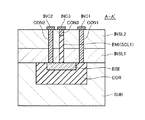
図1は、第1の実施形態に係る半導体装置SDの構成を示す斜視図である。図2は、半導体装置SDの平面図であり、図3は図2のA―A´断面図である。なお、図3においては、説明のため、絶縁膜INSL2より上の層及び各コンタクトを省略している。また、図1において、バイポーラトランジスタBPTを有する基板SUBと電界効果型トランジスタFETを有する基板SUBとを、説明のため互いに分離して示しているが、これらは一つの基板SUBである。
(First embodiment)
FIG. 1 is a perspective view showing the configuration of the semiconductor device SD according to the first embodiment. 2 is a plan view of the semiconductor device SD, and FIG. 3 is a cross-sectional view taken along the line AA ′ of FIG. In FIG. 3, for the sake of explanation, layers above the insulating film INSL2 and the contacts are omitted. Further, in FIG. 1, the substrate SUB having the bipolar transistor BPT and the substrate SUB having the field effect transistor FET are shown separately from each other for the sake of explanation, but these are one substrate SUB.
実施形態に係る半導体装置SDは、基板SUB、コレクタCOR(第1の第1導電型領域)、ベースBSE(第2導電型領域)、第1半導体層SCL1、エミッタEMI(第2の第1導電型領域)、第1コンタクトCON1、第2コンタクトCON2、及び第3コンタクトCON3を備えている。基板SUBは半導体基板である。コレクタCORは第1導電型の不純物領域であり、基板SUBに形成されている。ベースBSEは第2導電型の不純物領域であり、コレクタCORの表層に形成されている。第1半導体層SCL1はフィン型の半導体層であり、ベースBSEの上に位置している。エミッタEMIは第1半導体層SCL1に形成されており、底部がベースBSEに接続している。第1コンタクトCON1はコレクタCORに接続しており、第2コンタクトCON2はベースBSEに接続しており、第3コンタクトCON3はエミッタEMIに接続している。以下、詳細に説明する。 The semiconductor device SD according to the embodiment includes a substrate SUB, a collector COR (first first conductivity type region), a base BSE (second conductivity type region), a first semiconductor layer SCL1, and an emitter EMI (second first conductivity type). Mold region), a first contact CON1, a second contact CON2, and a third contact CON3. The substrate SUB is a semiconductor substrate. The collector COR is an impurity region of the first conductivity type and is formed on the substrate SUB. The base BSE is a second conductivity type impurity region and is formed on the surface layer of the collector COR. The first semiconductor layer SCL1 is a fin-type semiconductor layer and is located on the base BSE. The emitter EMI is formed in the first semiconductor layer SCL1, and the bottom is connected to the base BSE. The first contact CON1 is connected to the collector COR, the second contact CON2 is connected to the base BSE, and the third contact CON3 is connected to the emitter EMI. Details will be described below.
基板SUBは例えばシリコン基板である。そして、同一の基板SUBには、バイポーラトランジスタBPT及び電界効果型トランジスタFETが形成されている。本図に示す例において、基板SUBは第2導電型、例えばp型の半導体基板となっている。この場合、バイポーラトランジスタBPTのエミッタEMI及びコレクタCORはn型である。ただし、基板SUBがn型の半導体基板である場合、バイポーラトランジスタBPTのエミッタEMI及びコレクタCORはp型である。 The substrate SUB is, for example, a silicon substrate. A bipolar transistor BPT and a field effect transistor FET are formed on the same substrate SUB. In the example shown in the figure, the substrate SUB is a second conductivity type, for example, a p-type semiconductor substrate. In this case, the emitter EMI and the collector COR of the bipolar transistor BPT are n-type. However, when the substrate SUB is an n-type semiconductor substrate, the emitter EMI and the collector COR of the bipolar transistor BPT are p-type.
バイポーラトランジスタBPTは、バーティカル型のバイポーラトランジスタであり、上記したエミッタEMI、ベースBSE、及びコレクタCORを備えている。そしてバイポーラトランジスタBPTのエミッタEMIは、フィン型の第1半導体層SCL1を用いて形成されている。本図に示す例において、第1半導体層SCL1は第1導電型の半導体層になっており、第1半導体層SCL1の全体がエミッタEMIとなっている。ベースBSE及びコレクタCORは、基板SUBに不純物イオンを注入することにより形成されている。一方、エミッタEMIは、第1半導体層SCL1を形成した後、第1半導体層SCL1に不純物イオンを注入することにより、形成されている。 The bipolar transistor BPT is a vertical bipolar transistor and includes the emitter EMI, base BSE, and collector COR described above. The emitter EMI of the bipolar transistor BPT is formed using the fin-type first semiconductor layer SCL1. In the example shown in this drawing, the first semiconductor layer SCL1 is a first conductivity type semiconductor layer, and the entire first semiconductor layer SCL1 is an emitter EMI. The base BSE and the collector COR are formed by implanting impurity ions into the substrate SUB. On the other hand, the emitter EMI is formed by implanting impurity ions into the first semiconductor layer SCL1 after forming the first semiconductor layer SCL1.
電界効果型トランジスタFETはフィン型の第2半導体層SCL2を用いて形成されている。具体的には、基板SUBの上には、例えば酸化シリコン膜などの絶縁膜INSL1が形成されている。絶縁膜INSL1は、素子分離膜であり、第2半導体層SCL2よりも浅い。このため、第2半導体層SCL2は絶縁膜INSL1から出ている。そして電界効果型トランジスタFETのゲート電極GEは、第2半導体層SCL2の一部をまたぎつつ、絶縁膜INSL1の上に形成されている。なお、第1半導体層SCL1と第2半導体層SCL2は、同一方向に延在しているのが好ましい。また、絶縁膜INSL1は、基板SUBのうちバイポーラトランジスタBPTが形成されている領域にも形成されている。 The field effect transistor FET is formed using the fin-type second semiconductor layer SCL2. Specifically, an insulating film INSL1 such as a silicon oxide film is formed on the substrate SUB. The insulating film INSL1 is an element isolation film and is shallower than the second semiconductor layer SCL2. For this reason, the second semiconductor layer SCL2 protrudes from the insulating film INSL1. The gate electrode GE of the field effect transistor FET is formed on the insulating film INSL1 while straddling a part of the second semiconductor layer SCL2. Note that the first semiconductor layer SCL1 and the second semiconductor layer SCL2 preferably extend in the same direction. The insulating film INSL1 is also formed in a region of the substrate SUB where the bipolar transistor BPT is formed.
第2半導体層SCL2とゲート電極GEの間には、ゲート絶縁膜GINSが形成されている。ゲート絶縁膜GINSは、例えば第2半導体層SCL2を熱酸化することにより形成されている。そして第2半導体層SCL2のうちゲート電極GEで覆われていない領域には不純物が導入されている。これにより、第2半導体層SCL2にはソースSOUとなる第1不純物領域及びドレインDRNとなる第2不純物領域が形成される。言い換えると、ゲート絶縁膜GINS及びゲート電極GEは、第2半導体層SCL2のうち第1不純物領域及び第2不純物領域の間に位置する部分に形成されている。 A gate insulating film GINS is formed between the second semiconductor layer SCL2 and the gate electrode GE. The gate insulating film GINS is formed, for example, by thermally oxidizing the second semiconductor layer SCL2. An impurity is introduced into a region of the second semiconductor layer SCL2 that is not covered with the gate electrode GE. As a result, a first impurity region serving as the source SOU and a second impurity region serving as the drain DRN are formed in the second semiconductor layer SCL2. In other words, the gate insulating film GINS and the gate electrode GE are formed in a portion located between the first impurity region and the second impurity region in the second semiconductor layer SCL2.
そして、絶縁膜INSL1上には層間絶縁膜である絶縁膜INSL2が形成されている。絶縁膜INSL1及び絶縁膜INSL2には、第1コンタクトCON1、第2コンタクトCON2、第3コンタクトCON3、及びコンタクトCON4,CON5,CON6が埋め込まれている。第1コンタクトCON1はコレクタCORに接続しており、第2コンタクトCON2はベースBSEに接続しており、第3コンタクトCON3はエミッタEMIに接続している。またコンタクトCON4はゲート電極GEに接続しており、コンタクトCON5はドレインDRNに接続しており、コンタクトCON6はソースSOUに接続している。なお、これらコンタクトのレイアウトは、図2及び図3に示す例に限定されない。 An insulating film INSL2 that is an interlayer insulating film is formed over the insulating film INSL1. A first contact CON1, a second contact CON2, a third contact CON3, and contacts CON4, CON5, and CON6 are embedded in the insulating film INSL1 and the insulating film INSL2. The first contact CON1 is connected to the collector COR, the second contact CON2 is connected to the base BSE, and the third contact CON3 is connected to the emitter EMI. The contact CON4 is connected to the gate electrode GE, the contact CON5 is connected to the drain DRN, and the contact CON6 is connected to the source SOU. Note that the layout of these contacts is not limited to the example shown in FIGS.
そして、絶縁膜INSL2の上には第1配線INC1、第2配線INC2、及び第3配線INC3が形成されている。第1配線INC1は第1コンタクトCON1に接続しており、第2配線INC2は第2コンタクトCON2に接続しており、第3配線INC3は第3コンタクトCON3に接続している。第1配線INC1、第2配線INC2、及び第3配線INC3は、例えば絶縁膜INSL2の上に導電膜、例えばW膜などの金属膜を形成し、この導電膜を選択的に除去することによって形成されている。ただし、第1配線INC1、第2配線INC2、及び第3配線INC3は、ダマシン法によって形成されていても良い。 A first wiring INC1, a second wiring INC2, and a third wiring INC3 are formed on the insulating film INSL2. The first wiring INC1 is connected to the first contact CON1, the second wiring INC2 is connected to the second contact CON2, and the third wiring INC3 is connected to the third contact CON3. The first wiring INC1, the second wiring INC2, and the third wiring INC3 are formed by, for example, forming a conductive film, for example, a metal film such as a W film on the insulating film INSL2, and selectively removing the conductive film. Has been. However, the first wiring INC1, the second wiring INC2, and the third wiring INC3 may be formed by a damascene method.
なお、図示していないが、絶縁膜INSL2の上には、コンタクトCON4,CON5,CON6のそれぞれに接続する複数の配線も形成されている。これらの配線も、第1配線INC1と同一の工程で形成されている。 Although not shown, a plurality of wirings connected to the contacts CON4, CON5, and CON6 are also formed on the insulating film INSL2. These wirings are also formed in the same process as the first wiring INC1.
次に、図4〜図8を用いて、半導体装置SDの製造方法を説明する。各図において、(a)は図1に対応する斜視図であり、(b)は図3に対応する断面図である。 Next, a method for manufacturing the semiconductor device SD will be described with reference to FIGS. In each figure, (a) is a perspective view corresponding to FIG. 1, and (b) is a cross-sectional view corresponding to FIG.
まず、図4(a)及び(b)に示すように、第2導電型の基板SUBを準備する。次いで、基板SUBの上にレジストパターン(図示せず)を形成し、このレジストパターンをマスクとして第1導電型の不純物(例えばP)を基板SUBに注入する。これにより、コレクタCORが形成される。この工程における不純物の導入量は、例えば1×1013cm2以上1×1014cm2以下である。その後、レジストパターンを除去する。 First, as shown in FIGS. 4A and 4B, a second conductivity type substrate SUB is prepared. Next, a resist pattern (not shown) is formed on the substrate SUB, and a first conductivity type impurity (for example, P) is implanted into the substrate SUB using the resist pattern as a mask. Thereby, the collector COR is formed. The amount of impurities introduced in this step is, for example, 1 × 10 13 cm 2 or more and 1 × 10 14 cm 2 or less. Thereafter, the resist pattern is removed.
次いで、基板SUB上にレジストパターン(図示せず)を形成し、このレジストパターンをマスクとして第2導電型の不純物(例えばB)を基板SUBに注入する。これにより、基板SUBにはベースBSEが形成される。この工程における不純物の導入量は、例えば1×1012cm2以上1×1014cm2以下である。その後、レジストパターンを除去する。 Next, a resist pattern (not shown) is formed on the substrate SUB, and a second conductivity type impurity (for example, B) is implanted into the substrate SUB using the resist pattern as a mask. Thereby, the base BSE is formed on the substrate SUB. The amount of impurities introduced in this step is, for example, 1 × 10 12 cm 2 or more and 1 × 10 14 cm 2 or less. Thereafter, the resist pattern is removed.
次いで、図5(a)及び(b)に示すように、基板SUB上に、マスクパターンMSK1、例えば窒化シリコン膜などのハードマスクパターンを形成する。マスクパターンMSK1は、基板SUBのうち第1半導体層SCL1が形成されるべき領域及び第2半導体層SCL2が形成されるべき領域を覆っている。 Next, as shown in FIGS. 5A and 5B, a mask pattern MSK1, for example, a hard mask pattern such as a silicon nitride film, is formed on the substrate SUB. The mask pattern MSK1 covers a region of the substrate SUB where the first semiconductor layer SCL1 is to be formed and a region where the second semiconductor layer SCL2 is to be formed.
次いで、図6(a)及び(b)に示すように、マスクパターンMSK1をマスクとして、基板SUBをドライエッチングする。これにより、基板SUBには第1半導体層SCL1及び第2半導体層SCL2が形成される。 Next, as shown in FIGS. 6A and 6B, the substrate SUB is dry-etched using the mask pattern MSK1 as a mask. Thereby, the first semiconductor layer SCL1 and the second semiconductor layer SCL2 are formed on the substrate SUB.
その後、図7(a)及び(b)に示すように、基板SUB上に絶縁膜INSL1を形成する。絶縁膜INSL1は、例えばCVD法などの堆積法を用いて形成される。このとき、絶縁膜INSL1は第1半導体層SCL1及び第2半導体層SCL2よりも厚く形成される。ついで、絶縁膜INSL1を、CMP法などを用いて平坦化した後、絶縁膜INSL1をエッチングにより薄くして、絶縁膜INSL1から第1半導体層SCL1及び第2半導体層SCL2の上部を露出させる。その後、マスクパターンMSK1を除去する。 Thereafter, as shown in FIGS. 7A and 7B, an insulating film INSL1 is formed on the substrate SUB. The insulating film INSL1 is formed using a deposition method such as a CVD method. At this time, the insulating film INSL1 is formed thicker than the first semiconductor layer SCL1 and the second semiconductor layer SCL2. Next, after planarizing the insulating film INSL1 using a CMP method or the like, the insulating film INSL1 is thinned by etching, and the upper portions of the first semiconductor layer SCL1 and the second semiconductor layer SCL2 are exposed from the insulating film INSL1. Thereafter, the mask pattern MSK1 is removed.
次いで、図8(a)及び(b)に示すように、第2半導体層SCL2にゲート絶縁膜GINSを形成する。ゲート絶縁膜GINSは、例えば熱酸化法を用いて形成される。この場合、第1半導体層SCL1の表層にも熱酸化膜(図示せず)が形成される。次いで、基板SUB上にゲート電極GEとなる導電膜(例えばポリシリコン膜)を形成し、このポリシリコン膜を選択的に除去する。これにより、ゲート電極GEが形成される。次いで、ゲート電極GEをマスクとして第2半導体層SCL2に不純物を導入する。これにより、第2半導体層SCL2にソースSOU及びドレインDRNが形成される。 Next, as shown in FIGS. 8A and 8B, a gate insulating film GINS is formed in the second semiconductor layer SCL2. The gate insulating film GINS is formed using, for example, a thermal oxidation method. In this case, a thermal oxide film (not shown) is also formed on the surface layer of the first semiconductor layer SCL1. Next, a conductive film (for example, a polysilicon film) to be the gate electrode GE is formed on the substrate SUB, and this polysilicon film is selectively removed. Thereby, the gate electrode GE is formed. Next, impurities are introduced into the second semiconductor layer SCL2 using the gate electrode GE as a mask. Thereby, the source SOU and the drain DRN are formed in the second semiconductor layer SCL2.
なお、ソースSOU及びドレインDRNが第1導電型の不純物領域の場合、ソースSOU及びドレインDRNを形成する工程において、第1半導体層SCL1にも第1導電型の不純物を導入する。これにより、第1半導体層SCL1にエミッタEMIが形成される。 When the source SOU and the drain DRN are the first conductivity type impurity regions, the first conductivity type impurity is also introduced into the first semiconductor layer SCL1 in the step of forming the source SOU and the drain DRN. Thereby, an emitter EMI is formed in the first semiconductor layer SCL1.
一方、ソースSOU及びドレインDRNが第2導電型の不純物領域の場合、エミッタEMIは、ソースSOU及びドレインDRNとは別の不純物導入工程で形成される。この場合、ソースSOU及びドレインDRNを形成する工程において、第1半導体層SCL1はレジストパターンで覆われる。またエミッタEMIを形成する工程において、第2半導体層SCL2はレジストパターンで覆われる。 On the other hand, when the source SOU and the drain DRN are impurity regions of the second conductivity type, the emitter EMI is formed in a different impurity introduction process from the source SOU and the drain DRN. In this case, in the step of forming the source SOU and the drain DRN, the first semiconductor layer SCL1 is covered with a resist pattern. In the step of forming the emitter EMI, the second semiconductor layer SCL2 is covered with a resist pattern.
また、基板SUB上に複数の電界効果型トランジスタFETが形成されており、かつこれら複数の電界効果型トランジスタFETの一部が第1導電型であり、残りの電界効果型トランジスタFETが第2導電型である場合、エミッタEMIは、第1導電型の電界効果型トランジスタFETのソースSOU及びドレインDRNと同一工程で形成される。この場合、第1導電型の電界効果型トランジスタFETのソースSOU及びドレインDRNを形成する工程において、第2導電型の電界効果型トランジスタFETとなる第2半導体層SCL2はレジストパターンで覆われる。一方、第2導電型の電界効果型トランジスタFETのソースSOU及びドレインDRNを形成する工程において、第1導電型の電界効果型トランジスタFETとなる第2半導体層SCL2及び第1半導体層SCL1はレジストパターンで覆われる。 In addition, a plurality of field effect transistor FETs are formed on the substrate SUB, and a part of the plurality of field effect transistor FETs is the first conductivity type, and the remaining field effect transistor FETs are the second conductivity type. In the case of the type, the emitter EMI is formed in the same process as the source SOU and the drain DRN of the first conductivity type field effect transistor FET. In this case, in the step of forming the source SOU and the drain DRN of the first conductivity type field effect transistor FET, the second semiconductor layer SCL2 to be the second conductivity type field effect transistor FET is covered with a resist pattern. On the other hand, in the step of forming the source SOU and the drain DRN of the second conductivity type field effect transistor FET, the second semiconductor layer SCL2 and the first semiconductor layer SCL1 to be the first conductivity type field effect transistor FET are resist patterns. Covered with.
なお、いずれの場合においても、エミッタEMIを形成するときの不純物の導入量は、例えば1×1014cm2以上5×1016cm2以下である。 In any case, the amount of impurities introduced when forming the emitter EMI is, for example, 1 × 10 14 cm 2 or more and 5 × 10 16 cm 2 or less.
また、図8(b)に示す図において、エミッタEMIは、厚さ方向において第1半導体層SCL1の全体に形成されており、かつ基板SUBのうち第1半導体層SCL1以外の部分には形成されていない。ただし、図9(a)に示すように、エミッタEMIは、厚さ方向において第1半導体層SCL1の一部に形成されていても良いし、図9(b)に示すように、エミッタEMIは第1半導体層SCL1及び基板SUBのうち第1半導体層SCL1に接続する部分にも形成されていても良い。エミッタEMIの形成範囲は、例えばイオン注入時のエネルギーを調整することにより、変更することができる。 In FIG. 8B, the emitter EMI is formed on the entire first semiconductor layer SCL1 in the thickness direction, and is formed on a portion of the substrate SUB other than the first semiconductor layer SCL1. Not. However, as shown in FIG. 9A, the emitter EMI may be formed in a part of the first semiconductor layer SCL1 in the thickness direction. As shown in FIG. The first semiconductor layer SCL1 and the substrate SUB may also be formed on a portion connected to the first semiconductor layer SCL1. The formation range of the emitter EMI can be changed, for example, by adjusting the energy at the time of ion implantation.
以上、本実施形態によれば、フィン型の第1半導体層SCL1を用いてバイポーラトランジスタBPTを形成することができる。このため、バイポーラトランジスタBPTを微細化することができる。また、第1半導体層SCL1と同一工程で第2半導体層SCL2を形成し、さらにこの第2半導体層SCL2を用いてフィン型の電界効果型トランジスタFETを形成することができる。従って、少ない工程数で、同一の基板SUB上に、フィン型のバイポーラトランジスタBPTとフィン型の電界効果型トランジスタFETを形成することができる。 As described above, according to the present embodiment, the bipolar transistor BPT can be formed using the fin-type first semiconductor layer SCL1. For this reason, the bipolar transistor BPT can be miniaturized. Further, the second semiconductor layer SCL2 can be formed in the same process as the first semiconductor layer SCL1, and a fin-type field effect transistor FET can be formed using the second semiconductor layer SCL2. Therefore, the fin-type bipolar transistor BPT and the fin-type field effect transistor FET can be formed on the same substrate SUB with a small number of steps.
(第2の実施形態)
図10は、第2の実施形態に係る半導体装置SDの平面図であり、図11は図10のA−A´断面図である。図10は第1の実施形態における図2に対応しており、図11は第1の実施形態における図3に対応している。本実施形態に係る半導体装置SDは、以下の点を除いて第1の実施形態に係る半導体装置SDと同様の構成である。
(Second Embodiment)
FIG. 10 is a plan view of the semiconductor device SD according to the second embodiment, and FIG. 11 is a cross-sectional view taken along the line AA ′ of FIG. FIG. 10 corresponds to FIG. 2 in the first embodiment, and FIG. 11 corresponds to FIG. 3 in the first embodiment. The semiconductor device SD according to the present embodiment has the same configuration as the semiconductor device SD according to the first embodiment except for the following points.
まず、基板SUBは第1導電型、すなわちコレクタCORと同一導電型となっている。そして、基板SUBには、コレクタCORと基板SUBを電気的に分離するために、分離領域SEPが形成されている。分離領域SEPは第2導電型の不純物領域であり、コレクタCORの側面及び底面を覆っている。言い換えると、コレクタCORは分離領域SEPの一部に形成されている。 First, the substrate SUB has the first conductivity type, that is, the same conductivity type as the collector COR. In addition, an isolation region SEP is formed in the substrate SUB in order to electrically isolate the collector COR and the substrate SUB. The isolation region SEP is a second conductivity type impurity region and covers the side surface and the bottom surface of the collector COR. In other words, the collector COR is formed in a part of the isolation region SEP.
本実施形態に係る半導体装置SDの製造方法は、コレクタCORを形成する前(又は後)に、基板SUBに分離領域SEPを形成する点を除いて、第1の実施形態に示した半導体装置SDの製造方法と同様である。分離領域SEPは、例えば基板SUBにレジストパターンを形成し、このレジストパターンをマスクとして基板SUBに不純物を導入することにより、形成される。このときの不純物の導入量は、例えば5×1012cm2以上1×1013cm2以下である。 The manufacturing method of the semiconductor device SD according to the present embodiment is the same as that of the semiconductor device SD shown in the first embodiment except that the isolation region SEP is formed on the substrate SUB before (or after) the collector COR is formed. This is the same as the manufacturing method. The isolation region SEP is formed, for example, by forming a resist pattern on the substrate SUB and introducing impurities into the substrate SUB using the resist pattern as a mask. The amount of impurities introduced at this time is, for example, 5 × 10 12 cm 2 or more and 1 × 10 13 cm 2 or less.
本実施形態によっても、第1の実施形態と同様の効果が得られる。なお、第1の実施形態に示したバイポーラトランジスタBPTと、第2の実施形態に示したバイポーラトランジスタBPTとを、同一の基板SUB上に形成しても良い。 According to this embodiment, the same effect as that of the first embodiment can be obtained. Note that the bipolar transistor BPT shown in the first embodiment and the bipolar transistor BPT shown in the second embodiment may be formed on the same substrate SUB.
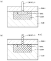
(第3の実施形態)
図12は、第3の実施形態に係る半導体装置SDの構成を示す斜視図である。図13は、半導体装置SDの平面図であり、図14は図13のB―B´断面図である。なお、図12〜図14は、それぞれ第1の実施形態における図1〜図3に対応しているが、これらの図において各コンタクトが省略されている。本実施形態に係る半導体装置SDは、バイポーラトランジスタBPTがラテラル型の構造を有している点を除いて、第1の実施形態に係る半導体装置SDと同様の構成である。
(Third embodiment)
FIG. 12 is a perspective view showing the configuration of the semiconductor device SD according to the third embodiment. 13 is a plan view of the semiconductor device SD, and FIG. 14 is a cross-sectional view taken along the line BB ′ of FIG. 12 to 14 correspond to FIGS. 1 to 3 in the first embodiment, respectively, but in these drawings, each contact is omitted. The semiconductor device SD according to the present embodiment has the same configuration as that of the semiconductor device SD according to the first embodiment, except that the bipolar transistor BPT has a lateral structure.
具体的には、バイポーラトランジスタBPTのベースBSE、エミッタEMI、及びコレクタCORは、いずれも第1半導体層SCL1に形成されている。エミッタEMI及びコレクタCORは互いに離間している。そして第1半導体層SCL1のうちエミッタEMI及びコレクタCORの間に位置する部分にはベースBSEが形成されている。言い換えると、ベースBSEは、エミッタEMI及びコレクタCORを互いに接続している。 Specifically, the base BSE, emitter EMI, and collector COR of the bipolar transistor BPT are all formed in the first semiconductor layer SCL1. The emitter EMI and the collector COR are separated from each other. A base BSE is formed in a portion of the first semiconductor layer SCL1 located between the emitter EMI and the collector COR. In other words, the base BSE connects the emitter EMI and the collector COR to each other.
そして基板SUBのうち第1半導体層SCL1の下に位置する部分には、ベースBSEの一部が形成されているが、第1の実施形態とは異なり、コレクタCORは形成されていない。 A part of the base BSE is formed in a portion of the substrate SUB located below the first semiconductor layer SCL1, but unlike the first embodiment, the collector COR is not formed.
図15(a)は、本実施形態に係る半導体装置SDの製造方法を説明するための斜視図であり、図15(b)は図15(a)のバイポーラトランジスタBPTの断面図である。図15(b)が示す断面は、図14が示す断面に相当している。本実施形態に係る半導体装置SDの製造方法は、以下の点を除いて第1の実施形態に係る半導体装置SDの製造方法と同様である。 FIG. 15A is a perspective view for explaining the method for manufacturing the semiconductor device SD according to the present embodiment, and FIG. 15B is a cross-sectional view of the bipolar transistor BPT in FIG. The cross section shown in FIG. 15B corresponds to the cross section shown in FIG. The manufacturing method of the semiconductor device SD according to the present embodiment is the same as the manufacturing method of the semiconductor device SD according to the first embodiment except for the following points.
まず、第1半導体層SCL1及び第2半導体層SCL2を形成する前(第1の実施形態における図4)に、基板SUBにコレクタCORを形成しない。ただし、ベースBSEは第1の実施形態と同様に形成される。このため、第1半導体層SCL1は、第2導電型を有している。 First, before forming the first semiconductor layer SCL1 and the second semiconductor layer SCL2 (FIG. 4 in the first embodiment), the collector COR is not formed on the substrate SUB. However, the base BSE is formed in the same manner as in the first embodiment. For this reason, the first semiconductor layer SCL1 has the second conductivity type.
そして、第1半導体層SCL1を形成した後、第1半導体層SCL1のうちベースBSEとなる領域をマスクパターンMSK2、例えばレジストパターンで覆う。次いで、マスクパターンMSK2をマスクとして第1半導体層SCL1に第1導電型の不純物を導入する。これにより、第1半導体層SCL1にはコレクタCOR及びエミッタEMIが形成される。なお、マスクパターンMSK2を形成して第1半導体層SCL1に第1導電型の不純物を導入するタイミングは、第1の実施形態において第1半導体層SCL1にエミッタEMIを形成するタイミングと同様である。 Then, after forming the first semiconductor layer SCL1, a region that becomes the base BSE in the first semiconductor layer SCL1 is covered with a mask pattern MSK2, for example, a resist pattern. Next, using the mask pattern MSK2 as a mask, a first conductivity type impurity is introduced into the first semiconductor layer SCL1. Thereby, the collector COR and the emitter EMI are formed in the first semiconductor layer SCL1. The timing at which the mask pattern MSK2 is formed and the first conductivity type impurity is introduced into the first semiconductor layer SCL1 is the same as the timing at which the emitter EMI is formed in the first semiconductor layer SCL1 in the first embodiment.
その後、マスクパターンMSK2を除去する。 Thereafter, the mask pattern MSK2 is removed.
なお、図14に示す図において、コレクタCOR及びエミッタEMIは、厚さ方向において第1半導体層SCL1の一部に形成されている。ただし、図16(a)に示すように、コレクタCOR及びエミッタEMIは、厚さ方向において第1半導体層SCL1の全体に形成されており、かつ基板SUBのうち第1半導体層SCL1以外の部分には形成されていないようにしてもよい。また、図16(b)に示すように、コレクタCOR及びエミッタEMIは第1半導体層SCL1及び基板SUBのうち第1半導体層SCL1に接続する部分にも形成されていても良い。コレクタCOR及びエミッタEMIの形成範囲は、例えばイオン注入時のエネルギーを調整することにより、変更することができる。 In the drawing shown in FIG. 14, the collector COR and the emitter EMI are formed in a part of the first semiconductor layer SCL1 in the thickness direction. However, as shown in FIG. 16A, the collector COR and the emitter EMI are formed on the entire first semiconductor layer SCL1 in the thickness direction, and are formed on portions of the substrate SUB other than the first semiconductor layer SCL1. May not be formed. Further, as shown in FIG. 16B, the collector COR and the emitter EMI may be formed in a portion of the first semiconductor layer SCL1 and the substrate SUB that is connected to the first semiconductor layer SCL1. The formation range of the collector COR and the emitter EMI can be changed by adjusting the energy at the time of ion implantation, for example.
本実施形態によれば、フィン型の第1半導体層SCL1を用いて、ラテラル型のバイポーラトランジスタBPTを形成することができる。 According to the present embodiment, the lateral bipolar transistor BPT can be formed using the fin-type first semiconductor layer SCL1.
(第4の実施形態)
図17は、第4の実施形態に係る半導体装置SDの平面図であり、図18は図17のB−B´断面図である。図17は第3の実施形態における図13に対応しており、図18は第3の実施形態における図14に対応している。本実施形態に係る半導体装置SDは、以下の点を除いて第3の実施形態に係る半導体装置SDと同様の構成である。
(Fourth embodiment)
FIG. 17 is a plan view of a semiconductor device SD according to the fourth embodiment, and FIG. 18 is a cross-sectional view taken along the line BB ′ of FIG. FIG. 17 corresponds to FIG. 13 in the third embodiment, and FIG. 18 corresponds to FIG. 14 in the third embodiment. The semiconductor device SD according to the present embodiment has the same configuration as the semiconductor device SD according to the third embodiment except for the following points.
まず、基板SUBは第1導電型、すなわちコレクタCORと同一導電型となっている。そして、基板SUBには、コレクタCORと基板SUBを電気的に分離するために、分離領域SEPが形成されている。分離領域SEPは、第2の実施形態と同様に、第2導電型の不純物領域であり、コレクタCORの側面及び底面を覆っている。言い換えると、コレクタCORは分離領域SEPの表層の一部に形成されている。 First, the substrate SUB has the first conductivity type, that is, the same conductivity type as the collector COR. In addition, an isolation region SEP is formed in the substrate SUB in order to electrically isolate the collector COR and the substrate SUB. As in the second embodiment, the isolation region SEP is a second conductivity type impurity region and covers the side surface and the bottom surface of the collector COR. In other words, the collector COR is formed in a part of the surface layer of the separation region SEP.
本実施形態に係る半導体装置SDの製造方法は、ベースBSEを形成する前(又は後)に、基板SUBに分離領域SEPを形成する点を除いて、第1の実施形態に示した半導体装置SDの製造方法と同様である。分離領域SEPの形成方法は、第2の実施形態と同様である。 The manufacturing method of the semiconductor device SD according to the present embodiment is the same as that of the semiconductor device SD shown in the first embodiment except that the isolation region SEP is formed on the substrate SUB before (or after) the base BSE is formed. This is the same as the manufacturing method. The method for forming the separation region SEP is the same as that in the second embodiment.
本実施形態によっても、第3の実施形態と同様の効果が得られる。なお、第3の実施形態に示したバイポーラトランジスタBPTと、第4の実施形態に示したバイポーラトランジスタBPTとを、同一の基板SUB上に形成しても良い。 According to this embodiment, the same effect as that of the third embodiment can be obtained. Note that the bipolar transistor BPT shown in the third embodiment and the bipolar transistor BPT shown in the fourth embodiment may be formed on the same substrate SUB.
(第5の実施形態)
図19は、第5の実施形態に係る半導体装置SDの構成を示す斜視図である。図20は、半導体装置SDの平面図であり、図21は図20のB―B´断面図である。なお、図19〜図21は、それぞれ第1の実施形態における図12〜図14に対応している。本実施形態に係る半導体装置SDは、バイポーラトランジスタBPTの上にマスクパターンMSK3が形成されている点を除いて、第3又は第4の実施形態に係る半導体装置SDと同様の構成である。なお、図19〜図21は、第3の実施形態と同様の場合を示している。
(Fifth embodiment)
FIG. 19 is a perspective view showing a configuration of a semiconductor device SD according to the fifth embodiment. 20 is a plan view of the semiconductor device SD, and FIG. 21 is a cross-sectional view taken along the line BB ′ of FIG. 19 to 21 correspond to FIGS. 12 to 14 in the first embodiment, respectively. The semiconductor device SD according to the present embodiment has the same configuration as the semiconductor device SD according to the third or fourth embodiment, except that a mask pattern MSK3 is formed on the bipolar transistor BPT. 19 to 21 show the same case as that of the third embodiment.
マスクパターンMSK3は、第3及び第4の実施形態におけるマスクパターンMSK2の代わりであり、第2導電型の第1半導体層SCL1に第1導電型の不純物を注入してコレクタCOR及びエミッタEMIを形成する工程において、マスクとして機能する。マスクパターンMSK3は、電界効果型トランジスタFETのゲート電極GEを形成する工程と同一工程で形成されているため、ゲート電極GEと同様の材料により形成されている。また、第1半導体層SCL1の上面及び側面には、ゲート絶縁膜GINSと同様の絶縁膜INSL3が形成されている。 The mask pattern MSK3 is a substitute for the mask pattern MSK2 in the third and fourth embodiments, and the first conductivity type impurity is implanted into the second conductivity type first semiconductor layer SCL1 to form the collector COR and the emitter EMI. In the process of performing, it functions as a mask. Since the mask pattern MSK3 is formed in the same process as the process of forming the gate electrode GE of the field effect transistor FET, it is formed of the same material as that of the gate electrode GE. Further, an insulating film INSL3 similar to the gate insulating film GINS is formed on the upper surface and side surfaces of the first semiconductor layer SCL1.
なお、図21に示す図において、コレクタCOR及びエミッタEMIは、厚さ方向において第1半導体層SCL1の一部に形成されている。ただし、図22(a)に示すように、コレクタCOR及びエミッタEMIは、厚さ方向において第1半導体層SCL1の全体に形成されており、かつ基板SUBのうち第1半導体層SCL1以外の部分には形成されていないようにしてもよい。また、図22(b)に示すように、コレクタCOR及びエミッタEMIは第1半導体層SCL1及び基板SUBのうち第1半導体層SCL1に接続する部分にも形成されていても良い。コレクタCOR及びエミッタEMIの形成範囲は、例えばイオン注入時のエネルギーを調整することにより、変更することができる。 In the drawing shown in FIG. 21, the collector COR and the emitter EMI are formed in a part of the first semiconductor layer SCL1 in the thickness direction. However, as shown in FIG. 22A, the collector COR and the emitter EMI are formed over the entire first semiconductor layer SCL1 in the thickness direction, and are formed on portions of the substrate SUB other than the first semiconductor layer SCL1. May not be formed. Further, as shown in FIG. 22B, the collector COR and the emitter EMI may be formed in a portion of the first semiconductor layer SCL1 and the substrate SUB that is connected to the first semiconductor layer SCL1. The formation range of the collector COR and the emitter EMI can be changed by adjusting the energy at the time of ion implantation, for example.
本実施形態によっても、第3の実施形態又は第4の実施形態と同様の効果が得られる。また、マスクパターンMSK3はゲート電極GEと同一工程で形成されるため、半導体装置SDを製造するときの工程数を少なくすることができる。また、マスクパターンMSK3はゲート電極GEと同程度の幅となるため、マスクパターンMSK3の幅を狭くして、ベースBSEの幅を狭くすることもできる。 According to the present embodiment, the same effect as that of the third embodiment or the fourth embodiment can be obtained. Further, since the mask pattern MSK3 is formed in the same process as the gate electrode GE, the number of processes when manufacturing the semiconductor device SD can be reduced. Further, since the mask pattern MSK3 has the same width as the gate electrode GE, the width of the base BSE can be narrowed by narrowing the width of the mask pattern MSK3.
(第6の実施形態)
図23は、第6の実施形態に係る半導体装置SDの構成を示す断面図であり、第5の実施形態における図21に対応している。本実施形態に係る半導体装置SDは、以下の点を除いて、第5の実施形態に係る半導体装置SDと同様の構成である。
(Sixth embodiment)
FIG. 23 is a cross-sectional view showing the configuration of the semiconductor device SD according to the sixth embodiment, and corresponds to FIG. 21 in the fifth embodiment. The semiconductor device SD according to the present embodiment has the same configuration as the semiconductor device SD according to the fifth embodiment except for the following points.
まず、マスクパターンMSK3の側面にサイドウォールSW1が形成されており、かつ第1半導体層SCL1の側面にサイドウォールSW2が形成されている。なお、本図には示していないが、ゲート電極GEの側面にもサイドウォールSW1が形成されており、かつ第2半導体層SCL2の側面にもサイドウォールSW2が形成されている。 First, the sidewall SW1 is formed on the side surface of the mask pattern MSK3, and the sidewall SW2 is formed on the side surface of the first semiconductor layer SCL1. Although not shown in the drawing, the sidewall SW1 is also formed on the side surface of the gate electrode GE, and the sidewall SW2 is also formed on the side surface of the second semiconductor layer SCL2.
また、絶縁膜INSL3は、第1半導体層SCL1のうちマスクパターンMSK3で覆われている部分、すなわちベースBSEの上にのみ形成されている。 The insulating film INSL3 is formed only on the portion of the first semiconductor layer SCL1 that is covered with the mask pattern MSK3, that is, on the base BSE.
本実施形態に係る半導体装置SDの製造方法は、第5の実施形態に示した半導体装置SDを製造する工程の後に、サイドウォールSW1,SW2を形成する工程を有している点を除いて、第5の実施形態に係る半導体装置SDの製造方法と同様である。サイドウォールSW1,SW2を形成する工程は、サイドウォールSW1,SW2となる絶縁膜を基板SUB上に形成する工程と、この絶縁膜をエッチバックしてサイドウォールSW1,SW2を形成する工程とを有している。 The manufacturing method of the semiconductor device SD according to the present embodiment has a process of forming the sidewalls SW1 and SW2 after the process of manufacturing the semiconductor device SD shown in the fifth embodiment, This is the same as the method for manufacturing the semiconductor device SD according to the fifth embodiment. The step of forming the sidewalls SW1 and SW2 includes a step of forming an insulating film to be the sidewalls SW1 and SW2 on the substrate SUB and a step of etching back the insulating film to form the sidewalls SW1 and SW2. doing.
本実施形態によっても、第5の実施形態と同様の効果が得られる。 According to this embodiment, the same effect as that of the fifth embodiment can be obtained.
(第7の実施形態)
図24は、第7の実施形態に係る半導体装置SDの平面図であり、図25は図24のB−B´断面図である。図24は第5の実施形態における図20に対応しており、図25は第5の実施形態における図21に対応している。本実施形態に係る半導体装置SDは、以下の点を除いて第5の実施形態に係る半導体装置SDと同様の構成である。
(Seventh embodiment)
FIG. 24 is a plan view of a semiconductor device SD according to the seventh embodiment, and FIG. 25 is a cross-sectional view taken along the line BB ′ of FIG. FIG. 24 corresponds to FIG. 20 in the fifth embodiment, and FIG. 25 corresponds to FIG. 21 in the fifth embodiment. The semiconductor device SD according to the present embodiment has the same configuration as the semiconductor device SD according to the fifth embodiment except for the following points.
まず、基板SUBは第1導電型、すなわちコレクタCORと同一導電型となっている。そして、基板SUBには、コレクタCORと基板SUBを電気的に分離するために、分離領域SEPが形成されている。分離領域SEPは、第2の実施形態と同様に、第2導電型の不純物領域であり、コレクタCORの側面及び底面を覆っている。言い換えると、コレクタCORは分離領域SEPの表層の一部に形成されている。 First, the substrate SUB has the first conductivity type, that is, the same conductivity type as the collector COR. In addition, an isolation region SEP is formed in the substrate SUB in order to electrically isolate the collector COR and the substrate SUB. As in the second embodiment, the isolation region SEP is a second conductivity type impurity region and covers the side surface and the bottom surface of the collector COR. In other words, the collector COR is formed in a part of the surface layer of the separation region SEP.
本実施形態に係る半導体装置SDの製造方法は、ベースBSEを形成する前(又は後)に、基板SUBに分離領域SEPを形成する点を除いて、第5の実施形態に示した半導体装置SDの製造方法と同様である。分離領域SEPの形成方法は、第2の実施形態と同様である。 The manufacturing method of the semiconductor device SD according to the present embodiment is the same as that of the semiconductor device SD shown in the fifth embodiment except that the isolation region SEP is formed on the substrate SUB before (or after) the base BSE is formed. This is the same as the manufacturing method. The method for forming the separation region SEP is the same as that in the second embodiment.
本実施形態によっても、第5の実施形態と同様の効果が得られる。なお、第5の実施形態に示したバイポーラトランジスタBPTと、第7の実施形態に示したバイポーラトランジスタBPTとを、同一の基板SUB上に形成しても良い。 According to this embodiment, the same effect as that of the fifth embodiment can be obtained. Note that the bipolar transistor BPT shown in the fifth embodiment and the bipolar transistor BPT shown in the seventh embodiment may be formed on the same substrate SUB.
以上、本発明者によってなされた発明を実施の形態に基づき具体的に説明したが、本発明は前記実施の形態に限定されるものではなく、その要旨を逸脱しない範囲で種々変更可能であることはいうまでもない。 As mentioned above, the invention made by the present inventor has been specifically described based on the embodiment. However, the present invention is not limited to the embodiment, and various modifications can be made without departing from the scope of the invention. Needless to say.
BPT バイポーラトランジスタ
BSE ベース
CON1 第1コンタクト
CON2 第2コンタクト
CON3 第3コンタクト
CON4 コンタクト
CON5 コンタクト
CON6 コンタクト
COR コレクタ
DRN ドレイン
EMI エミッタ
FET 電界効果型トランジスタ
GE ゲート電極
GINS ゲート絶縁膜
INC1 第1配線
INC2 第2配線
INC3 第3配線
INSL1 絶縁膜
INSL2 絶縁膜
INSL3 絶縁膜
MSK1 マスクパターン
MSK2 マスクパターン
MSK3 マスクパターン
SCL1 第1半導体層
SCL2 第2半導体層
SD 半導体装置
SEP 分離領域
SOU ソース
SUB 基板
SW1 サイドウォール
SW2 サイドウォール
BPT bipolar transistor BSE base CON1 first contact CON2 second contact CON3 third contact CON4 contact CON5 contact CON6 contact COR collector DRN drain EMI emitter FET field effect transistor GE gate electrode GINS gate insulating film INC1 first wiring INC2 second wiring INC3 Third wiring INSL1 Insulating film INSL2 Insulating film INSL3 Insulating film MSK1 Mask pattern MSK2 Mask pattern MSK3 Mask pattern SCL1 First semiconductor layer SCL2 Second semiconductor layer SD Semiconductor device SEP Isolation region SOU Source SUB Substrate SW1 Side wall SW2 Side wall
Claims (5)
前記半導体基板に形成された第1の第1導電型領域と、
前記第1の第1導電型領域の表層に形成された第2導電型領域と、
前記第2導電型領域の上に位置する第1半導体層と、
前期第1半導体層に形成されており、底部が前記第2導電型領域に接続している第2の第1導電型領域と、
前記第1の第1導電型領域に接続する第1コンタクトと、
前記第2導電型領域に接続する第2コンタクトと、
前記第2の第1導電型領域に接続する第3コンタクトと、
を備え、
前記半導体基板は第1導電型であり、
さらに、前記半導体基板に形成され、前記第1の第1導電型領域の側面及び底面を囲む第2導電型の分離領域を備える半導体装置。 A semiconductor substrate;
A first first conductivity type region formed in the semiconductor substrate;
A second conductivity type region formed in a surface layer of the first first conductivity type region;
A first semiconductor layer located on the second conductivity type region;
A second first conductivity type region formed in the first semiconductor layer in the previous period and having a bottom connected to the second conductivity type region;
A first contact connected to the first first conductivity type region;
A second contact connected to the second conductivity type region;
A third contact connected to the second first conductivity type region;
With
The semiconductor substrate is of a first conductivity type;
And a second conductivity type isolation region formed on the semiconductor substrate and surrounding a side surface and a bottom surface of the first first conductivity type region.
前記半導体基板に形成された第1の第1導電型領域と、
前記第1の第1導電型領域の表層に形成された第2導電型領域と、
前記第2導電型領域の上に位置する第1半導体層と、
前期第1半導体層に形成されており、底部が前記第2導電型領域に接続している第2の第1導電型領域と、
前記第1の第1導電型領域に接続する第1コンタクトと、
前記第2導電型領域に接続する第2コンタクトと、
前記第2の第1導電型領域に接続する第3コンタクトと、
前記半導体基板のうち前記第1半導体層とは異なる場所に形成された第2半導体層と、
前記第2半導体層に形成され、ソースとなる第1不純物領域と、
前記第2半導体層に形成され、前記第1不純物領域から離れており、ドレインとなる第2不純物領域と、
前記第2半導体層のうち前記第1不純物領域と前記第2不純物領域の間に位置する部分に形成されたゲート絶縁膜と、
前記ゲート絶縁膜上に形成されたゲート電極と、
を備える半導体装置。 A semiconductor substrate;
A first first conductivity type region formed in the semiconductor substrate;
A second conductivity type region formed in a surface layer of the first first conductivity type region;
A first semiconductor layer located on the second conductivity type region;
A second first conductivity type region formed in the first semiconductor layer in the previous period and having a bottom connected to the second conductivity type region;
A first contact connected to the first first conductivity type region;
A second contact connected to the second conductivity type region;
A third contact connected to the second first conductivity type region;
A second semiconductor layer formed at a location different from the first semiconductor layer in the semiconductor substrate;
A first impurity region formed in the second semiconductor layer and serving as a source;
A second impurity region formed in the second semiconductor layer, separated from the first impurity region and serving as a drain;
A gate insulating film formed in a portion of the second semiconductor layer located between the first impurity region and the second impurity region;
A gate electrode formed on the gate insulating film;
A semiconductor device comprising:
前記基板の一部の上に形成された第1半導体層と、
前記第1半導体層に形成された第1の第1導電型領域と、
前記第1半導体層に形成され、前記第1の第1導電型領域から離れている第2の第1導電型領域と、
前記第1半導体層に形成され、前記第1の第1導電型領域と前記第2の第1導電型領域とを接続する第2導電型領域と、
を備え、
前記基板は第1導電型の半導体基板であり、
さらに、前記半導体基板に形成され、前記第1半導体層の底面を囲む第2導電型の分離領域を備える半導体装置。 A substrate,
A first semiconductor layer formed on a portion of the substrate;
A first first conductivity type region formed in the first semiconductor layer;
A second first conductivity type region formed in the first semiconductor layer and separated from the first first conductivity type region;
A second conductivity type region formed in the first semiconductor layer and connecting the first first conductivity type region and the second first conductivity type region;
With
The substrate is a first conductivity type semiconductor substrate;
Further, a semiconductor device comprising a second conductivity type isolation region formed on the semiconductor substrate and surrounding a bottom surface of the first semiconductor layer.
前記基板のうち前記第1半導体層とは異なる場所に形成された第2半導体層と、
前記第2半導体層に形成され、ソースとなる第1不純物領域と、
前記第2半導体層に形成され、前記第1不純物領域から離れており、ドレインとなる第2不純物領域と、
前記第2半導体層のうち前記第1不純物領域と前記第2不純物領域の間に位置する部分に形成されたゲート絶縁膜と、
前記ゲート絶縁膜上に形成されたゲート電極と、
を備える半導体装置。 The semiconductor device according to claim 3 .
A second semiconductor layer formed at a location different from the first semiconductor layer in the substrate;
A first impurity region formed in the second semiconductor layer and serving as a source;
A second impurity region formed in the second semiconductor layer, separated from the first impurity region and serving as a drain;
A gate insulating film formed in a portion of the second semiconductor layer located between the first impurity region and the second impurity region;
A gate electrode formed on the gate insulating film;
A semiconductor device comprising:
前記第1半導体層の上面に形成された絶縁層と、
前記絶縁層を挟んで前記第2導電型領域の上に位置する被覆膜と、
を備え、
前記被覆膜は、前記ゲート電極と同一の材料によって形成されている半導体装置。 The semiconductor device according to claim 4 ,
An insulating layer formed on an upper surface of the first semiconductor layer;
A coating film located on the second conductivity type region across the insulating layer;
With
The said coating film is a semiconductor device formed with the same material as the said gate electrode.
Priority Applications (2)
| Application Number | Priority Date | Filing Date | Title |
|---|---|---|---|
| JP2014087027A JP6219224B2 (en) | 2014-04-21 | 2014-04-21 | Semiconductor device |
| US14/679,051 US9461036B2 (en) | 2014-04-21 | 2015-04-06 | Semiconductor device |
Applications Claiming Priority (1)
| Application Number | Priority Date | Filing Date | Title |
|---|---|---|---|
| JP2014087027A JP6219224B2 (en) | 2014-04-21 | 2014-04-21 | Semiconductor device |
Publications (3)
| Publication Number | Publication Date |
|---|---|
| JP2015207649A JP2015207649A (en) | 2015-11-19 |
| JP2015207649A5 JP2015207649A5 (en) | 2016-11-10 |
| JP6219224B2 true JP6219224B2 (en) | 2017-10-25 |
Family
ID=54322662
Family Applications (1)
| Application Number | Title | Priority Date | Filing Date |
|---|---|---|---|
| JP2014087027A Active JP6219224B2 (en) | 2014-04-21 | 2014-04-21 | Semiconductor device |
Country Status (2)
| Country | Link |
|---|---|
| US (1) | US9461036B2 (en) |
| JP (1) | JP6219224B2 (en) |
Families Citing this family (4)
| Publication number | Priority date | Publication date | Assignee | Title |
|---|---|---|---|---|
| US10665702B2 (en) | 2017-12-27 | 2020-05-26 | Samsung Electronics Co., Ltd. | Vertical bipolar transistors |
| FR3087047B1 (en) | 2018-10-08 | 2021-10-22 | St Microelectronics Sa | BIPOLAR TRANSISTOR |
| FR3087048B1 (en) * | 2018-10-08 | 2021-11-12 | St Microelectronics Sa | BIPOLAR TRANSISTOR |
| FR3113539B1 (en) | 2020-08-24 | 2022-09-23 | St Microelectronics Crolles 2 Sas | bipolar transistor |
Family Cites Families (9)
| Publication number | Priority date | Publication date | Assignee | Title |
|---|---|---|---|---|
| JP2768719B2 (en) * | 1988-11-21 | 1998-06-25 | 株式会社日立製作所 | Semiconductor device and semiconductor storage device |
| US4868135A (en) * | 1988-12-21 | 1989-09-19 | International Business Machines Corporation | Method for manufacturing a Bi-CMOS device |
| JPH0344937A (en) * | 1989-07-13 | 1991-02-26 | Nippon Telegr & Teleph Corp <Ntt> | Bipolar transistor and manufacture thereof |
| JPH0590278A (en) | 1991-09-30 | 1993-04-09 | Nec Corp | Semiconductor device |
| JP2005236084A (en) | 2004-02-20 | 2005-09-02 | Toshiba Corp | Vertical bipolar transistor and its manufacturing method |
| US7288829B2 (en) * | 2004-11-10 | 2007-10-30 | International Business Machines Corporation | Bipolar transistor with self-aligned retrograde extrinsic base implant profile and self-aligned silicide |
| JP2007165780A (en) | 2005-12-16 | 2007-06-28 | Toshiba Corp | Semiconductor device |
| JP2011119344A (en) | 2009-12-01 | 2011-06-16 | Panasonic Corp | Semiconductor apparatus, and method for manufacturing the same |
| US20110147840A1 (en) | 2009-12-23 | 2011-06-23 | Cea Stephen M | Wrap-around contacts for finfet and tri-gate devices |
-
2014
- 2014-04-21 JP JP2014087027A patent/JP6219224B2/en active Active
-
2015
- 2015-04-06 US US14/679,051 patent/US9461036B2/en not_active Expired - Fee Related
Also Published As
| Publication number | Publication date |
|---|---|
| JP2015207649A (en) | 2015-11-19 |
| US20150303189A1 (en) | 2015-10-22 |
| US9461036B2 (en) | 2016-10-04 |
Similar Documents
| Publication | Publication Date | Title |
|---|---|---|
| KR101393917B1 (en) | A cmos device and method of forming the same | |
| US8497548B2 (en) | Semiconductor device including a MOS transistor and production method therefor | |
| TWI542007B (en) | Device and method for manufacturing the same | |
| US7442619B2 (en) | Method of forming substantially L-shaped silicide contact for a semiconductor device | |
| CN103378153A (en) | Structure and method for finfet integrated with capacitor | |
| JP2010171055A (en) | Semiconductor device and method of manufacturing the same | |
| JP6219224B2 (en) | Semiconductor device | |
| KR20130083923A (en) | Method for producing semiconductor device and semiconductor device | |
| US9000513B2 (en) | Method for manufacturing a semiconductor device and semiconductor device with surrounding gate transistor | |
| WO2013171873A1 (en) | Semiconductor device | |
| JP5692886B1 (en) | Semiconductor device manufacturing method and semiconductor device | |
| JP5596245B1 (en) | Semiconductor device manufacturing method and semiconductor device | |
| US8664050B2 (en) | Structure and method to improve ETSOI MOSFETS with back gate | |
| US10290728B2 (en) | Semiconductor device and manufacturing method thereof | |
| JP4565847B2 (en) | Semiconductor device and manufacturing method thereof | |
| JP2013045953A (en) | Semiconductor device and method of manufacturing the same | |
| JP5286318B2 (en) | Semiconductor device | |
| JP5749818B2 (en) | Semiconductor device manufacturing method and semiconductor device | |
| TW201301442A (en) | Method for fabricating a conductive contact | |
| US9502508B2 (en) | Method for manufacturing isolation structure integrated with semiconductor device | |
| JP5936653B2 (en) | Semiconductor device | |
| JP5928566B2 (en) | Semiconductor device manufacturing method and semiconductor device | |
| KR20130093149A (en) | Production method of semiconductor device and semiconductor device | |
| JP5685344B2 (en) | Semiconductor device manufacturing method and semiconductor device | |
| JP2010165942A (en) | Semiconductor device, and method of manufacturing the same |
Legal Events
| Date | Code | Title | Description |
|---|---|---|---|
| A521 | Written amendment |
Free format text: JAPANESE INTERMEDIATE CODE: A523 Effective date: 20160923 |
|
| A621 | Written request for application examination |
Free format text: JAPANESE INTERMEDIATE CODE: A621 Effective date: 20160923 |
|
| A977 | Report on retrieval |
Free format text: JAPANESE INTERMEDIATE CODE: A971007 Effective date: 20170518 |
|
| A131 | Notification of reasons for refusal |
Free format text: JAPANESE INTERMEDIATE CODE: A131 Effective date: 20170530 |
|
| A521 | Written amendment |
Free format text: JAPANESE INTERMEDIATE CODE: A523 Effective date: 20170721 |
|
| TRDD | Decision of grant or rejection written | ||
| A01 | Written decision to grant a patent or to grant a registration (utility model) |
Free format text: JAPANESE INTERMEDIATE CODE: A01 Effective date: 20170905 |
|
| A61 | First payment of annual fees (during grant procedure) |
Free format text: JAPANESE INTERMEDIATE CODE: A61 Effective date: 20170927 |
|
| R150 | Certificate of patent or registration of utility model |
Ref document number: 6219224 Country of ref document: JP Free format text: JAPANESE INTERMEDIATE CODE: R150 |