JP6211409B2 - Display device - Google Patents
Display device Download PDFInfo
- Publication number
- JP6211409B2 JP6211409B2 JP2013254209A JP2013254209A JP6211409B2 JP 6211409 B2 JP6211409 B2 JP 6211409B2 JP 2013254209 A JP2013254209 A JP 2013254209A JP 2013254209 A JP2013254209 A JP 2013254209A JP 6211409 B2 JP6211409 B2 JP 6211409B2
- Authority
- JP
- Japan
- Prior art keywords
- detection
- electrode
- circuit
- display device
- detection electrode
- Prior art date
- Legal status (The legal status is an assumption and is not a legal conclusion. Google has not performed a legal analysis and makes no representation as to the accuracy of the status listed.)
- Active
Links
Images


Classifications
-
- G—PHYSICS
- G06—COMPUTING; CALCULATING OR COUNTING
- G06F—ELECTRIC DIGITAL DATA PROCESSING
- G06F3/00—Input arrangements for transferring data to be processed into a form capable of being handled by the computer; Output arrangements for transferring data from processing unit to output unit, e.g. interface arrangements
- G06F3/01—Input arrangements or combined input and output arrangements for interaction between user and computer
- G06F3/03—Arrangements for converting the position or the displacement of a member into a coded form
- G06F3/041—Digitisers, e.g. for touch screens or touch pads, characterised by the transducing means
- G06F3/0412—Digitisers structurally integrated in a display
-
- G—PHYSICS
- G06—COMPUTING; CALCULATING OR COUNTING
- G06F—ELECTRIC DIGITAL DATA PROCESSING
- G06F3/00—Input arrangements for transferring data to be processed into a form capable of being handled by the computer; Output arrangements for transferring data from processing unit to output unit, e.g. interface arrangements
- G06F3/01—Input arrangements or combined input and output arrangements for interaction between user and computer
- G06F3/03—Arrangements for converting the position or the displacement of a member into a coded form
- G06F3/041—Digitisers, e.g. for touch screens or touch pads, characterised by the transducing means
- G06F3/0416—Control or interface arrangements specially adapted for digitisers
- G06F3/04166—Details of scanning methods, e.g. sampling time, grouping of sub areas or time sharing with display driving
-
- G—PHYSICS
- G06—COMPUTING; CALCULATING OR COUNTING
- G06F—ELECTRIC DIGITAL DATA PROCESSING
- G06F3/00—Input arrangements for transferring data to be processed into a form capable of being handled by the computer; Output arrangements for transferring data from processing unit to output unit, e.g. interface arrangements
- G06F3/01—Input arrangements or combined input and output arrangements for interaction between user and computer
- G06F3/03—Arrangements for converting the position or the displacement of a member into a coded form
- G06F3/041—Digitisers, e.g. for touch screens or touch pads, characterised by the transducing means
- G06F3/044—Digitisers, e.g. for touch screens or touch pads, characterised by the transducing means by capacitive means
- G06F3/0443—Digitisers, e.g. for touch screens or touch pads, characterised by the transducing means by capacitive means using a single layer of sensing electrodes
Description
本開示は、表示装置に関し、例えば、タッチパネルを内蔵したインセル方式の液晶表示装置に適用可能である。 The present disclosure relates to a display device and can be applied to, for example, an in-cell liquid crystal display device including a touch panel.
表示画面に使用者の指またはペンなどを用いてタッチ操作(接触押圧操作、以下、単にタッチと称する)して情報を入力する装置(以下、タッチセンサ又はタッチパネルとも称する)を備えた表示装置は、PDAや携帯端末などのモバイル用電子機器、各種の家電製品、現金自動預け払い機(Automated Teller Machine)等に用いられている。
このようなタッチパネルとして、タッチされた部分の容量変化を検出する静電容量方式が知られている。この静電容量方式タッチパネルとして、タッチパネル機能を液晶表示パネルに内蔵した、所謂、インセル方式の液晶表示装置が知られている(例えば、特開2009−258182号公報)。インセル方式の液晶表示装置では、タッチパネルの走査電極として、液晶表示パネルを構成するTFT基板上に形成される対向電極(コモン電極ともいう)を分割して使用している。
A display device provided with a device (hereinafter also referred to as a touch sensor or a touch panel) for inputting information by performing a touch operation (contact pressing operation, hereinafter simply referred to as touch) using a user's finger or pen on a display screen. It is used in mobile electronic devices such as PDAs and portable terminals, various home appliances, and automated teller machines.
As such a touch panel, a capacitive system that detects a change in capacitance of a touched portion is known. As this capacitance type touch panel, a so-called in-cell type liquid crystal display device in which a touch panel function is built in a liquid crystal display panel is known (for example, JP 2009-258182 A). In an in-cell type liquid crystal display device, a counter electrode (also referred to as a common electrode) formed on a TFT substrate constituting a liquid crystal display panel is divided and used as a scanning electrode of a touch panel.
従来のアウトセル方式タッチパネルを使用する液晶表示装置では、液晶表示パネルの表示動作をオフし、タッチパネルを疎検出モードにして、低消費電力モードを実現している。低消費電力モードのときに、タッチや移動(スワイプ(Swipe))を行うと、検出情報はタッチパネルコントローラICからホストコントローラに送信され、ホストコントローラは通常表示/通常検出モードに遷移する。
タッチパネル機能を内蔵したインセル方式の液晶表示装置は、共通電極を、タッチパネルの走査電極と兼用しているので、液晶表示パネルの表示動作を停止させた状態で、走査電極のスキャンを行うと、液晶表示パネルの液晶層に直流電圧が印加され、液晶層に焼き付きが発生してしまうという問題点がある。
本開示の課題は、タッチパネル機能を内蔵したインセル方式の表示装置において、表示動作の停止中に、タッチパネルの検出を可能とする技術を提供することにある。
その他の課題と新規な特徴は、本明細書の記述及び添付図面によって明らかにする。
In a liquid crystal display device using a conventional out-cell type touch panel, the display operation of the liquid crystal display panel is turned off, and the touch panel is set to a sparse detection mode to realize a low power consumption mode. When touching or moving (Swipe) in the low power consumption mode, detection information is transmitted from the touch panel controller IC to the host controller, and the host controller transitions to the normal display / normal detection mode.
Since the in-cell type liquid crystal display device with a built-in touch panel function uses the common electrode also as the scan electrode of the touch panel, when the scan electrode is scanned while the display operation of the liquid crystal display panel is stopped, the liquid crystal display device There is a problem in that a DC voltage is applied to the liquid crystal layer of the display panel, and image sticking occurs in the liquid crystal layer.
An object of the present disclosure is to provide a technique that enables detection of a touch panel while a display operation is stopped in an in-cell display device incorporating a touch panel function.
Other problems and novel features will become apparent from the description of this specification and the accompanying drawings.
本開示のうち、代表的なものの概要を簡単に説明すれば、下記の通りである。
表示装置は、アレイ基板と、対向基板と、検出回路と、を備える。前記表示装置は、第1のモードと、第2のモードと、を有する。前記アレイ基板は、画素電極と、共通電極と、を有する。前記対向基板は、第1の検出電極と、第2の検出電極と、を有する。前記第1の検出電極は、前記第2の検出電極と交互に配置される。前記第1のモードでは、前記共通電極は表示の電極とタッチパネルの走査電極を兼用するようにされ、コモン電圧と第1の走査パルス電圧とが供給され、前記検出回路は、前記第1および第2の検出電極で検出される検出電圧に基づきタッチ位置を検出するようにされる。前記第2のモードでは、前記第1の検出電極は仮走査電極として機能させられ、前記検出回路は、前記第1の検出電極に第2の走査パルス電圧を供給するようにされ、前記第2の検出電極で検出される検出電圧に基づきスワイプの有無を検出するようにされる。
The outline of a representative one of the present disclosure will be briefly described as follows.
The display device includes an array substrate, a counter substrate, and a detection circuit. The display device has a first mode and a second mode. The array substrate has a pixel electrode and a common electrode. The counter substrate includes a first detection electrode and a second detection electrode. The first detection electrodes are alternately arranged with the second detection electrodes. In the first mode, the common electrode serves as a display electrode and a scan electrode of the touch panel, a common voltage and a first scan pulse voltage are supplied, and the detection circuit includes the first and second scan electrodes. The touch position is detected based on the detection voltage detected by the two detection electrodes. In the second mode, the first detection electrode is caused to function as a provisional scan electrode, the detection circuit is configured to supply a second scan pulse voltage to the first detection electrode, and the second mode The presence or absence of swipe is detected based on the detection voltage detected by the detection electrodes.
以下に、実施例について、図面を参照しつつ説明する。なお、開示はあくまで一例にすぎず、当業者において、発明の主旨を保っての適宜変更について容易に想到し得るものについては、当然に本発明の範囲に含有されるものである。また、図面は説明をより明確にするため、実際の態様に比べ、各部の幅、厚さ、形状等について模式的に表される場合があるが、あくまで一例であって、本発明の解釈を限定するものではない。また、本明細書と各図において、既出の図に関して前述したものと同様の要素には、同一の符号を付して、詳細な説明を適宜省略することがある。 Hereinafter, examples will be described with reference to the drawings. It should be noted that the disclosure is merely an example, and those skilled in the art can easily conceive of appropriate modifications while maintaining the gist of the invention are naturally included in the scope of the present invention. In addition, the drawings may be schematically represented with respect to the width, thickness, shape, and the like of each part in comparison with actual aspects for the sake of clarity of explanation, but are merely examples, and the interpretation of the present invention is not limited. It is not limited. In addition, in the present specification and each drawing, elements similar to those described above with reference to the previous drawings are denoted by the same reference numerals, and detailed description may be omitted as appropriate.
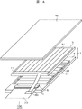
実施例1に係る表示装置は、表示パネルの内部にタッチパネルを内蔵したインセル方式の表示装置である。実施例1に係る表示装置の構造について、図1および図2を用いて説明する。
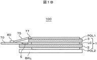
図1Aは実施例1に係る表示装置の概略構成を示す分解斜視図である。図1Bは実施例1に係る表示装置の断面図である。図2は実施例1に係る表示装置の概略構成を示す平面図である。
図1Aおよび図1Bに示すように、表示装置100は、表示パネル1と、ドライバIC5と、フレキシブル配線基板70と、フロントウィンドウ(又は保護フィルム)40と、フレキシブル配線基板75と、バックライトBKLと、を有する。表示パネル1は、TFT基板(アレイ基板)2と、CF基板(対向基板)3と、偏光板POL1、POL2と、を有する。CF基板3上の裏面側透明導電膜(CD)を、帯状(ストライプ状)のパターンに分割して、タッチパネルの検出電極31となし、TFT基板2の内部に形成される共通電極(対向電極)21を帯状のパターンに分割、即ち、複数のブロックに分割して、タッチパネルの走査電極として兼用することにより、通常のタッチパネルで使用されるタッチパネル基板を削減している。また、表示装置100では、タッチパネル駆動用および検出用の回路が、ドライバIC5の内部に設けられる。ドライバIC5は、1つの半導体基板上にCMOSプロセスで形成され、半導体チップの形態でTFT基板2上にCOG実装される。
The display device according to the first embodiment is an in-cell display device in which a touch panel is built in a display panel. The structure of the display device according to Example 1 will be described with reference to FIGS.
FIG. 1A is an exploded perspective view illustrating a schematic configuration of the display device according to the first embodiment. FIG. 1B is a cross-sectional view of the display device according to the first embodiment. FIG. 2 is a plan view illustrating a schematic configuration of the display device according to the first embodiment.
As shown in FIGS. 1A and 1B, the
図2に示すように、共通電極(COMMON)21はTFT基板2上に設けられているが、例えば20本の共通電極21が両端で共通に接続され、共通電極信号線22と接続されている。表示装置100では、帯状の共通電極21が走査電極Txを兼用し、また、検出電極31の一部が仮走査電極Tx’を兼用する。1つの共通電極21は、例えば64ライン分の画素に共通して用いられる。したがって、共通電極信号には、画像表示に用いられるコモン電圧と、タッチ位置の検出に用いられる走査パルス電圧とが含まれる。走査パルス電圧が共通電極21に印加されると、共通電極21と一定の間隔を持って配置され容量を構成する検出電極31に検出信号が生じる。この検出信号は、図1Aに示すように、接続部77、フレキシブル配線基板75、コネクタ80、フレキシブル配線基板70を介してドライバIC5に取り出される。また、TFT基板2には共通電極信号線22以外にもゲートスキャン回路6や走査信号線7、映像信号線8、フレキシブル配線基板70との接続端子であるドライバIC5用入力端子9のような様々な回路や配線、端子等が形成される。なお、図1Aでは、図が複雑になるのを避けるために、共通電極21は9本、検出電極31は8本のみ示されており、また、図2に示されるゲートスキャン回路6等が省略されている。図2では、図が複雑になるのを避けるために、RGBの映像信号を選択するセレクタ回路が省略されている。
As shown in FIG. 2, the common electrode (COMMON) 21 is provided on the
TFT基板2には画素部20が設けられており、画素電極と共通電極21は画素の一部として画像表示に用いられる。1つの共通電極は、複数の画素(例えば64ラインの画素)に共通に用いられる。また、TFT基板2とCF基板3との間には液晶層LCが狭持される。CF基板3に設けられた検出電極31とTFT基板に設けられた共通電極21とは容量を形成しており、共通電極21に駆動信号が印加されると検出電極31の電圧が変化する。この時、フロントウィンドウ40を介して指等の導電体が近接または接触すると、容量に変化が生じ検出電極31に生じる電圧に、近接・接触が無い場合に比較して変化が生じる。このように、表示パネルに形成した共通電極21と検出電極31との間に生じる容量の変化を検出することで、表示パネルにタッチパネルの機能を備えることが可能となる。
A
<ミューチュアル検出>
実施例1に係る表示装置の表示動作状態におけるタッチパネル機能(ミューチュアル検出、第一ミューチャル検出)について、図3から図7Bを用いて説明する。ミューチュアル検出は、表示動作状態で、画素を構成する共通電極21はタッチパネルの走査電極を共用し、走査電極と検出電極との交差容量の容量変化を検出し、タッチ位置を検出する。例えば、1フレームの表示中に表示とタッチ検出を時分割で行うことは表示動作状態に含まれる。すなわち、表示動作状態では、共通電極は表示とタッチ検出に時分割で使用することが可能である。共通電極が表示とタッチ検出に時分割で使用する状態を第1のモードという。表示動作状態は第1のモードである。
図3は実施例1に係る表示装置の表示動作状態における、タッチパネルの全体概略構成を示すブロック図である。図4は実施例1に係る表示装置の表示動作状態における、タッチパネルのタッチ検出動作のタイミング図である。図5は実施例1に係る検出回路のより具体的な回路構成を示す回路図である。図6は実施例1に係る検出回路の表示動作状態における動作を説明するためのタイミングチャートである。図7Aは実施例1に係る表示装置の表示動作状態における、表示およびタッチスキャン(分割Vブランク駆動)の模式図である。図7Bは実施例1に係る表示装置の表示動作状態における、分割Vブランク駆動タイミングを示す図である。
<Mutual detection>
The touch panel function (mutual detection, first mutual detection) in the display operation state of the display device according to the first embodiment will be described with reference to FIGS. 3 to 7B. In the mutual detection, in the display operation state, the
FIG. 3 is a block diagram illustrating an overall schematic configuration of the touch panel in the display operation state of the display device according to the first embodiment. FIG. 4 is a timing diagram of the touch detection operation of the touch panel in the display operation state of the display device according to the first embodiment. FIG. 5 is a circuit diagram illustrating a more specific circuit configuration of the detection circuit according to the first embodiment. FIG. 6 is a timing chart for explaining the operation in the display operation state of the detection circuit according to the first embodiment. FIG. 7A is a schematic diagram of display and touch scan (divided V blank drive) in the display operation state of the display device according to the first embodiment. FIG. 7B is a diagram illustrating divided V blank drive timing in the display operation state of the display device according to the first embodiment.
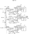
表示装置100のタッチパネル機能は、駆動回路101と、シーケンサ102と、走査パルス電圧生成回路103と、デコーダ回路106と、タッチパネル107と、検出回路108とで構成される。なお、図3において、タッチパネル107を除いた回路は、ドライバIC5内にある。
タッチパネル107には、ユーザのタッチを検出するためのセンサ端子である電極パターン(走査電極Tx1〜Tx8、検出電極Rx1〜Rx6)が形成されている。以下、走査電極Txは走査電極Tx1〜Txmの、検出電極Rxは検出電極Rx1〜Rxnの総称である。表示装置100は、タッチパネル機能が表示パネル1に内蔵されているため、共通電極21が走査電極Txを兼用している。なお、図面が複雑になるのを避けるため、図3では、走査電極Tx1〜Tx8は8本および検出電極Rx1〜Rx6は6本のみ示されている。
駆動回路101は、表示パネル1に画像を表示するための同期信号(垂直同期信号(Vsync)及び水平同期信号(Hsync))をシーケンサ102へ送出する。シーケンサ102は、走査パルス電圧生成回路103、デコーダ回路106、及び検出回路108を制御して、タッチ検出動作のタイミングを制御する。
走査パルス電圧生成回路103は、走査電極Tx1〜Tx8を駆動するための走査パルス電圧(VTX)を生成して出力する。
The touch panel function of the
On the
The
The scan pulse
デコーダ回路106は、シーケンサ102から入力される選択信号に基づいて、走査パルス電圧(VTX)を、走査電極Tx1〜Tx8の中1つの走査電極へ出力するアナログスイッチ(デマルチプレクサ)である。
検出回路108は、走査電極Tx1〜Tx8の中で、走査パルス電圧(VTX)が供給されている1つの走査電極と、各検出電極Rx1〜Rx6との交点における電極間容量(相互容量、交差容量)Cxyを検出する。
シーケンサ102は、走査パルス電圧生成回路103等を制御し、垂直同期信号(Vsync)及び水平同期信号(Hsync)に同期しながら、走査電極Tx1〜Tx8へ順次走査パルス電圧(VTX)を供給する。ここで、図3、図4に示すように、各走査電極Tx1〜Tx8には、走査パルス電圧(VTX)が複数回供給される。なお、図面が複雑になるのを避けるため、図4では、走査パルス電圧(VTX)は8回のみ示されている。限定するものではないが、走査パルス電圧(VTX)は20〜40回供給されるのが好ましい。
The
The
The
図4に示すように、検出回路108は、各検出電極Rx1〜Rx6に流れる電流を積算し(図4では負方向への積算)、到達した電圧値(ΔVa,ΔVb)を記録する。
走査電極Txと検出電極Rxとの交点付近を、指(導体)がタッチしている場合、指へも電流が流れるため、積算結果の電圧値に変化が生じる。
例えば、図4のNAに示すように、走査電極Tx1と検出電極Rx1との交点付近に指が存在しない(タッチ無しの状態の)場合、検出電極Rx1に流れる電流を積算した電圧(ΔVa)は、非タッチレベルLAとなる。
これに対して、図4のNBに示すように、走査電極Tx2と検出電極Rx1との交点付近には指が存在する(タッチ有りの状態の)場合、指へも電流が流れ、検出電極Rx1に流れる電流を積算した電圧(ΔVb)は、非タッチレベルLAよりもVST高い電位の電圧となる。この変化量(タッチ信号)によりタッチ位置(座標)を検出することができる。
As shown in FIG. 4, the
When the finger (conductor) is touching the vicinity of the intersection of the scanning electrode Tx and the detection electrode Rx, a current flows to the finger, so that the voltage value of the integration result changes.
For example, as indicated by NA in FIG. 4, when a finger does not exist near the intersection of the scanning electrode Tx1 and the detection electrode Rx1 (in a state without touch), the voltage (ΔVa) obtained by integrating the current flowing through the detection electrode Rx1 is The non-touch level LA.
On the other hand, as shown by NB in FIG. 4, when a finger is present near the intersection of the scanning electrode Tx2 and the detection electrode Rx1 (in a touched state), a current also flows to the finger, and the detection electrode Rx1 A voltage (ΔVb) obtained by integrating the currents flowing through is a voltage having a potential higher by V ST than the non-touch level LA. The touch position (coordinates) can be detected from this change amount (touch signal).
以下、図5および図6を用いて、ミューチュアル検出時の検出回路108の動作を説明する。なお、図6のTXは走査電極Txである。
検出回路108は、積分回路10と、サンプルホールド回路11と、10ビットのAD変換器(ADC)12と、AD変換器12から出力されるデータ(以下、RAWデータ)を格納するメモリ(RAM)13と、キャリブレーションデータを格納するメモリ(RAM)14と、8ビットのDA変換器(DAC)15と、マイクロコンピュータ(MPU)16とを有する。積分回路10はスイッチS1と積分容量Cintとオペアンプを有する。サンプルホールド回路11はスイッチS4と容量Cshとオペアンプを有する。検出回路108は、さらに、キャリブレーション容量Cclb、スイッチS2、S3、S5、S6を有する。ここで、スイッチS1は、スイッチS1_Rx1〜S1_Rxnのn個のスイッチの総称である。スイッチS2、S3、S4、S5、S6も同様である。
Hereinafter, the operation of the
The
(1)検出電極および積分回路のリセット(図6のA1の期間)
各検出電極Rx1〜Rxnに流れる電流を検出(積分)前に、スイッチS2、S4をオフ(OFF)し、スイッチS1をオン(ON)して、積分回路10をリセットするとともに、スイッチS3をONとして、各検出電極Rx1〜Rxnをリセットする。
基準電圧(VREF)を4V(VREF=4V)とすると、積分回路10の出力は4V、各検出電極Rx1〜Rxnは、4Vにプリチャージされる。
また、スイッチS5は、基準電圧(VOFSC)側に接続されており、キャリブレーション容量Cclbの両端には、基準電圧(VOFSC)の4Vが印加されているため、キャリブレーション容量Cclbの電荷は「0」である。
(1) Detection electrode and integration circuit reset (period A1 in FIG. 6)
Before detecting (integrating) the current flowing through each of the detection electrodes Rx1 to Rxn, the switches S2 and S4 are turned off (OFF), the switch S1 is turned on (ON), the integrating
When the reference voltage (V REF ) is 4 V (V REF = 4 V), the output of the integrating
The switch S5 is connected to the reference voltage (V OFSC ) side, and 4 V of the reference voltage (V OFSC ) is applied to both ends of the calibration capacitor Cclb. Therefore, the charge of the calibration capacitor Cclb is “0”.
(2)積分(図6のB1の期間)
次に、スイッチS1とスイッチS3をOFFとした後、走査電極Tx1〜Txmの1つへ走査パルス電圧(VTX)を出力し、スイッチS5をDA変換器15側に切り替え、キャリブレーション容量Cclbの一端に、DA変換器15から出力されるキャリブレーション電圧(VDAC)を印加し、電荷の引き抜きを行った後に、スイッチS2をONとして残りの電荷を積分容量Cintに積分する。
これにより、走査電極Tx1〜Txmの1つを、交差容量Cxy、積分容量Cintの経路で電流が流れ、積分回路10の出力電圧(VINT)が低下する。VINTは下記の式で表される。
VINT=VREF−(VTX*CXY−VCLB*CCLB)/CINT
ここで、CXYは交差容量Cxyの容量値、CCLBはキャリブレーション容量Cclbの容量智、CINTは積分容量Cintの容量値である。積分容量Cintの電荷は、交差容量Cxyの電荷から−キャリブレーション容量Cclbの電荷を差し引いたものである。
(2) Integration (period B1 in FIG. 6)
Next, after the switches S1 and S3 are turned OFF, the scanning pulse voltage (V TX ) is output to one of the scanning electrodes Tx1 to Txm, the switch S5 is switched to the
As a result, a current flows through one of the scan electrodes Tx1 to Txm through the path of the cross capacitance Cxy and the integration capacitance Cint, and the output voltage (V INT ) of the
V INT = V REF − (V TX * C XY −V CLB * C CLB ) / C INT
Here, C XY is the capacitance value of the cross capacitance Cxy, C CLB is the capacitance value of the calibration capacitance Cclb, and C INT is the capacitance value of the integration capacitance Cint. The charge of the integration capacitor Cint is obtained by subtracting the charge of the −calibration capacitor Cclb from the charge of the cross capacitor Cxy.
(3)検出電極のリセット(図6のA2の期間)
積分回路10での積分終了後、スイッチS2をOFF、スイッチS3をONとして、スイッチS5を基準電圧(VOFSC)側に接続して、各検出電極Rx1〜Rxnを4Vにプリチャージするとともに、キャリブレーション容量Cclbの電荷を「0」とする。
(4)上記(2)の積分回路10での積分動作を繰り返し、電圧を積み上げる(図6のB2,…Bnの期間)。
(3) Detection electrode reset (period A2 in FIG. 6)
After integration in the
(4) The integration operation in the
(5)サンプル&ホールド(図6のCの期間)
積分回路10での積分完了後(図6のBnの期間後)、スイッチS4をONとして、サンプルホールド回路11でサンプル&ホールドし、その後、スイッチS6を順次ONとして、AD変換器12でAD変換し、メモリ(RAM)13に、走査電極Rx1〜Rxn分のRAWデータを格納する。
AD変換器12が、10bitのAD変換器の場合、RAWデータは0(積分0V)〜1023(積分4V)の範囲となる。
(5) Sample and hold (period C in FIG. 6)
After the integration in the
When the
(6)上記(1)〜(5)の処理を、全ての走査電極Tx1〜Txmについて順次実行し、各走査電極Tx1〜Txmと各検出電極Rx1〜Rxnの交点1面分のRAWデータをメモリ13に格納する。 (6) The processes (1) to (5) are sequentially executed for all the scan electrodes Tx1 to Txm, and RAW data for one intersection surface of each of the scan electrodes Tx1 to Txm and each of the detection electrodes Rx1 to Rxn is stored in memory. 13.
(7)交差容量Cxyの容量値は非タッチ時の方がタッチ時よりも大きいので、図4のΔVa、ΔVbに示すように、積分回路10での積分出力電圧(VINT)の降下に差が生じ、ここにしきい値を設けて、タッチ位置を検出する。
(7) Since the capacitance value of the cross capacitance Cxy is larger at the time of non-touch than at the time of touch, there is a difference in the drop in the integrated output voltage (V INT ) in the
次に、キャリブレーションについて説明する。
前述したように、各走査電極Tx1〜Txmと各検出電極Rx1〜Rxnの交点の交差容量Cxyは、液晶層、ガラス基板、偏光板、接着樹脂などの誘電率や厚みのばらつき、また不均一性のため、個体差や面内ばらつきを持つため、キャリブレーションが必須である。
Next, calibration will be described.
As described above, the cross capacitance Cxy at the intersections of the scan electrodes Tx1 to Txm and the detection electrodes Rx1 to Rxn is a variation in dielectric constant or thickness of the liquid crystal layer, glass substrate, polarizing plate, adhesive resin, etc. Therefore, calibration is essential because of individual differences and in-plane variations.
(1)非タッチ時RAWデータ動作点を255とし、マイクロコンピュータ(MPU)16は、これをキャリブレーション目標値として、メモリ(RAM)14のキャリブレーションデータを書き換え、DA変換器15から出力されるキャリブレーション電圧(VDAC)を可変しながら収束させる。
なお、非タッチ時のRAWデータ動作点とは、非タッチ時の積分回路10での積分出力電圧(VINT)を、サンプルホールド回路11でサンプル&ホールドし、10ビットのAD変換器12でAD変換したときのRAWデータであることは言うまでもない。
(1) The RAW data operating point at the time of non-touch is set to 255, and the microcomputer (MPU) 16 rewrites the calibration data in the memory (RAM) 14 using this as a calibration target value and is output from the
Note that the RAW data operating point at the time of non-touch means that the integration output voltage (V INT ) at the
(2)キャリブレーションは動作点を移動させる作用のみで、検出感度には影響しない。検出感度は下記の式で表され、キャリブレーション電圧(VDAC)を含まない。
検出感度=(ΔCXY/CINT)*VTX
ΔCXY=CXY_UT−CXY_T
ここで、CXY_UTは非タッチ時の交差容量CXYの容量値、CXY_Tはタッチ時の交差容量CXYの容量値である。
なお、通常、キャリブレーション範囲が、8ビットで[8’h80]の付近、即ち、基準電圧(VREF=4V)とGND(0V)の電圧の中間付近の電圧となるように、キャリブレーション容量Cclbの容量値(CCLB)を決定する。また、通常、キャリブレーション容量Cclbは、ダイオード接続されたMOSトランジスタの接合容量を利用するので、キャリブレーション容量Cclbの容量値(CCLB)の増減は、ダイオード接続されたMOSトランジスタが、並列に接続される個数で調整する。
(2) Calibration only moves the operating point and does not affect the detection sensitivity. The detection sensitivity is expressed by the following equation and does not include the calibration voltage (V DAC ).
Detection sensitivity = (ΔC XY / C INT ) * V TX
ΔC XY = C XY_UT −C XY_T
Here, C XY_UT the capacitance value of the intersection capacitance C XY of untouched, C XY_T is the capacitance value of the intersection capacitance C XY in-touch.
Normally, the calibration capacitance is set so that the calibration range is in the vicinity of [8′h80] with 8 bits, that is, a voltage in the vicinity of the midpoint between the reference voltage (V REF = 4V) and GND (0V). The capacity value (C CLB ) of Cclb is determined. In general, since the calibration capacitor Cclb uses the junction capacitance of a diode-connected MOS transistor, the capacitance value (C CLB ) of the calibration capacitor Cclb increases or decreases when the diode-connected MOS transistor is connected in parallel. Adjust the number of
図7Aおよび図7Bを用いて、分割Vブランク駆動によるタッチパネル検出時と、画素書込み時のタイミングを説明する。
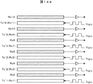
1垂直期間(1V period)または1フレームの表示期間は、映像信号や走査信号(Sig)が駆動される期間(表示期間ブロック71)と、タッチパネルの走査パルス電圧(VTX)が駆動される期間(タッチ期間ブロック72)に分割され、交互に駆動される。これを分割Vブランク駆動という。1フレームの表示期間は、N個の表示期間ブロック(Display)71とN個のタッチ期間ブロック(Touch)72を有する。1表示期間ブロックでは、例えば1280/Nラインがスキャンされ、1タッチ期間ブロックでは、20/M本の走査電極(共通電極)がスキャンされる。例えば、N=20、M=20の場合、1表示期間ブロックでは64ラインがスキャンされ、1タッチ期間ブロックでは1本の走査電極がスキャンされる。1本の走査電極には20〜40回走査パルス電圧が印加される。ここでMは自然数であり、Nよりも大きくても同じでも小さくてもよい。1垂直期間におけるタッチ検出回数を多く(たとえば4回)としたい場合はN=20、M=5とすれば、1垂直期間に4回のタッチ検出を全ての共通電極21にて行うことが可能となり、検出精度が上がる。1垂直期間におけるタッチ検出回数を少なく(たとえば1/2回、2垂直期間に1回)としたい場合はN=20、M=40とすれば、2垂直期間に1回のタッチ検出を全ての共通電極21にて行うこととなり、タッチ検出における消費電力が低減される。このNやMの値は後の図8に出てくる駆動回路101のレジスタにホストコントローラ200から値が設定されることにより定められる。
図7Aおよび図7Bに示すように、共通電極を走査電極Txとして機能させているので、タッチパネル検出時のスキャン動作は、画素書き込みを行うゲートスキャンを行っていない期間で行う。映像信号線8と共通電極21との間、および、走査信号線7と共通電極21との間には寄生容量があるため、映像信号線8上の電圧(VDL)の変動、あるいは、走査信号線7上の電圧(VGL)の立ち上がり、あるいは、立ち下り時に生じるノイズにより、タッチパネル検出時の検出レベルが変動し、座標精度が低下する。したがって、タッチ位置検出動作は、映像信号線8上の電圧(VDL)の変動、あるいは、走査信号線7上の電圧(VGL)の立ち上がり、あるいは、立ち下りがない期間に実行する必要がある。分割Vブランク駆動では、タッチ位置検出動作を、映像信号線8上の電圧(VDL)の変動、あるいは、走査信号線7上の電圧(VGL)の立ち上がり、あるいは、立ち下りがない期間に実行することが容易である。1フレーム期間において、映像信号や走査信号(Sig)が駆動される期間を1回のみとし、タッチパネルの走査パルス電圧(VTX)が駆動される期間を1回のみとした場合、走査パルス電圧の駆動期間を長く設ける必要がでるが、それは1フレームに設けられるブランキング期間の制約もあり困難な場合が多い。分割Vブランク駆動ではそのような事態も避けられる。
7A and 7B, the timing at the time of touch panel detection by divided V blank drive and the timing at pixel writing will be described.
One vertical period (1 V period) or one frame display period includes a period during which a video signal and a scanning signal (Sig) are driven (display period block 71) and a period during which the scanning pulse voltage (V TX ) of the touch panel is driven. It is divided into (touch period block 72) and driven alternately. This is called divided V blank drive. The display period of one frame includes N display period blocks (Display) 71 and N touch period blocks (Touch) 72. In one display period block, for example, 1280 / N lines are scanned, and in one touch period block, 20 / M scan electrodes (common electrodes) are scanned. For example, when N = 20 and M = 20, 64 lines are scanned in one display period block, and one scan electrode is scanned in one touch period block. A scan pulse voltage is applied 20 to 40 times to one scan electrode. Here, M is a natural number and may be larger, the same or smaller than N. When it is desired to increase the number of touch detections in one vertical period (for example, 4 times), if N = 20 and M = 5, touch detection can be performed four times in one vertical period by all the
As shown in FIGS. 7A and 7B, since the common electrode functions as the scan electrode Tx, the scan operation at the time of detecting the touch panel is performed during a period when the gate scan for pixel writing is not performed. Since there is a parasitic capacitance between the
<疑似ミューチュアル検出>
次に表示動作停止状態のタッチパネル機能(疑似ミューチュアル検出、第二ミューチャル検出)について、図8から図12Bを用いて説明する。疑似ミューチュアル検出は、表示動作停止状態で、対向基板側にある検出電極のみを用いて、検出電極間の容量の容量変化を検出し、タッチ検出または横移動検出する。横移動(スワイプ検出)とは、検出電極の長手方向に垂直な方向(短手方向)成分の移動を検出することをいう。表示動作停止状態では、共通電極は表示用にもタッチ検出用にも使用されない。共通電極が表示用にもタッチ検出用にも使用されない状態を第2のモードという。表示動作およびその他不要な回路を停止する低消費電力モード(以下、「スリープモード」という。)は、第2のモードである。スリープモードでは、バックライトが消灯される。
<Pseudo-mutual detection>
Next, the touch panel function (pseudo-mutual detection, second mutual detection) in the display operation stop state will be described with reference to FIGS. 8 to 12B. In the pseudo-mutual detection, the change in capacitance between the detection electrodes is detected by using only the detection electrodes on the counter substrate side in the display operation stop state, and touch detection or lateral movement detection is performed. Lateral movement (swipe detection) refers to detection of movement of a component perpendicular to the longitudinal direction of the detection electrode (short direction). In the display operation stop state, the common electrode is not used for display or touch detection. A state in which the common electrode is not used for display or touch detection is referred to as a second mode. The low power consumption mode (hereinafter referred to as “sleep mode”) in which the display operation and other unnecessary circuits are stopped is the second mode. In the sleep mode, the backlight is turned off.
図8は実施例1に係る表示装置の表示動作停止状態における、タッチパネルの全体概略構成を示すブロック図である。図9Aは実施例1に係る検出回路の表示動作停止状態における、動作を説明するための図である。図9Bは実施例1に係る検出回路の表示動作停止状態における、タッチパネルのタッチ検出動作のタイミング図である。図9Cは実施例1に係る検出回路における、基準電圧の設定レジスタを示す図である。図9Dは実施例1に係る検出回路における、キャリブレーション電圧とメモリデータとの関係を示す図である。図10は実施例1に係る検出回路の表示動作停止状態における、各信号のタイミングを示す図である。図11は実施例1に係る検出回路のスワイプ操作におけるタッチ信号変化を示す図である。図12Aは実施例1に係る表示装置のシングルタッチ起動またはダブルタッチ起動を説明するための図である。図12Bは実施例1に係る表示装置のスワイプ起動を説明するための図である。 FIG. 8 is a block diagram illustrating an overall schematic configuration of the touch panel in a display operation stop state of the display device according to the first embodiment. FIG. 9A is a diagram for explaining the operation in the display operation stop state of the detection circuit according to the first embodiment. FIG. 9B is a timing diagram of the touch detection operation of the touch panel in the display operation stop state of the detection circuit according to the first embodiment. FIG. 9C is a diagram illustrating a reference voltage setting register in the detection circuit according to the first embodiment. FIG. 9D is a diagram illustrating a relationship between the calibration voltage and the memory data in the detection circuit according to the first embodiment. FIG. 10 is a diagram illustrating the timing of each signal in the display operation stop state of the detection circuit according to the first embodiment. FIG. 11 is a diagram illustrating a touch signal change in the swipe operation of the detection circuit according to the first embodiment. FIG. 12A is a diagram for explaining single touch activation or double touch activation of the display device according to the first embodiment. FIG. 12B is a diagram for explaining swipe activation of the display device according to the first embodiment.
図8に示すように、表示動作停止状態では、タッチパネルの検出電極Rxの中で、一つおきの検出電極Rxを仮走査電極T’xとして機能させ、検出回路108は、仮走査電極T’xに走査パルス電圧(VQTX)を出力する。図8では、検出電極Rx1を仮走査電極T’x1、検出電極Rx3を仮走査電極T’x2、検出電極Rx5を仮走査電極T’x3として動作させる。すなわち、奇数番目の検出電極Rx_Oddを仮走査電極T’xとして動作させる。なお、表示動作停止状態では、走査電極Tx(共通電極21)はGND電位に固定される。
As shown in FIG. 8, in the display operation stop state, every other detection electrode Rx among the detection electrodes Rx of the touch panel functions as the temporary scanning electrode T′x, and the
また、表示装置100を表示動作状態から表示動作停止状態に遷移させる場合、ホストコントローラ200は、ドライバIC5内のレジスタに所定のデータを設定することにより、図9Aに示すように、仮走査電極T’x(奇数番目の検出電極Rx_Odd)に接続されるスイッチS2_ODDをOFFとし、かつ、スイッチS2_ODDに接続される積分回路10とサンプルホールド回路11をOFFとする。ここで、積分回路10とサンプルホールド回路11をOFFするということは、積分回路10およびサンプルホールド回路11の各ノードを基準電位(基準電圧またはGND)に固定し貫通電流を流さないようにすることである。同様に、ドライバIC5内のレジスタに設定された所定のデータにより、スイッチS7_ODDを順次ONとして、仮走査電極T’xに、順次走査パルス電圧(VQTX)を供給する。ここで、仮走査電極T’xには、走査パルス電圧(VQTX)が複数回(例えば、64回;1回当たりの時間は、6us)供給される。
Further, when the
前述の図4で説明した表示動作状態と同様に、スイッチS2_EVENに接続される偶数番目の積分回路10は、偶数番目の各検出電極Rx_Evenに流れる電流を積算し(本実施例では負方向への積算)、到達した電圧値(ΔVa’,ΔVb’)を記録する。
偶数番目の各検出電極Rx_Evenと、仮走査電極T’x(奇数番目の検出電極Rx_Odd)と、を指(導体)がタッチしている場合、あるいは、偶数番目の各検出電極Rx_Evenと、仮走査電極T’x1,T’x2,T’x3に、指(導体)が近接した場合、指へも電流が流れるため、偶数番目の各検出電極Rx2,Rx4,Rx6に流れる電流を積分した積算結果の電圧値に変化が生じる。
偶数番目の各検出電極Rx2,Rx4,Rx6と、仮走査電極T’x1,T’x2,T’x3と、に指が近接していない場合、図9BのNAに示すように、検出電極に流れる電流を積算した電圧(ΔVa’)は、非タッチレベルLA’となる。
これに対して、偶数番目の各検出電極Rx2,Rx4,Rx6と、仮走査電極T’x1,T’x2,T’x3と、を指がタッチしている場合、図9BのNBに示すように、指へも電流が流れるので、偶数番目の各検出電極Rx2,Rx4,Rx6に流れる電流を積算した電圧(ΔVb’)は、非タッチレベルLA’よりも高電位の電圧となる。この変化量(タッチ信号)によりタッチまたはスワイプの有無を検出することができる。
Similar to the display operation state described above with reference to FIG. 4, the even-
When the finger (conductor) touches each even-numbered detection electrode Rx_Even and the provisional scanning electrode T′x (odd-numbered detection electrode Rx_Odd), or each even-numbered detection electrode Rx_Even and provisional scanning When a finger (conductor) comes close to the electrodes T′x1, T′x2, and T′x3, a current flows also to the finger. Therefore, an integration result obtained by integrating the currents flowing through the even-numbered detection electrodes Rx2, Rx4, and Rx6. A change occurs in the voltage value.
When the finger is not close to the even-numbered detection electrodes Rx2, Rx4, Rx6 and the temporary scanning electrodes T′x1, T′x2, T′x3, as shown by NA in FIG. The voltage (ΔVa ′) obtained by integrating the flowing current becomes the non-touch level LA ′.
On the other hand, when the finger touches the even-numbered detection electrodes Rx2, Rx4, Rx6 and the temporary scanning electrodes T′x1, T′x2, T′x3, as shown by NB in FIG. 9B. In addition, since a current also flows to the finger, a voltage (ΔVb ′) obtained by integrating the currents flowing through the even-numbered detection electrodes Rx2, Rx4, and Rx6 becomes a voltage having a higher potential than the non-touch level LA ′. The presence or absence of touch or swipe can be detected from this change amount (touch signal).
以下、図9A、図9C、図9Dおよび図10を用いて、疑似ミューチュアル検出時の検出回路108の動作を説明する。
検出回路108は、積分回路10と、サンプルホールド回路11と、キャリブレーションアンプ17と、を有する。キャリブレーションアンプ17には、図9Cに示すような基準電圧の設定レジスタ(TPC_VOFSCTX)に基づいた電圧(VOFSC)、または図9Cに示すようなメモリ14に格納されるキャリブレーションデータ(CLB_DATA)に基づいたDA変換器15の出力電圧(キャリブレーション電圧(VDAC))が供給される。
Hereinafter, the operation of the
The
(1)検出電極および積分回路のリセット(図10のA1の期間)
スイッチS2_ODDとスイッチS3_ODDをOFFし、スイッチS7_ODDをONして、検出電極Rx_Oddを仮走査電極T’xとして使用できるようにする。また、スイッチS5_ODDは、VDAC側(VDAC=0.25V)に接続されており、走査パルス電圧(VQTX=0.25V)を出力し、検出電極Rx_Oddは0.25Vにリセットされる。ここで、スイッチS1_ODDは、スイッチS1_Rx1、S1_Rx3、S1_Rx5の奇数番目の検出電極Rx_Oddに接続されるスイッチの総称である。スイッチS2_ODD、S3_ODD、S4_ODD、S5_ODD、S6_ODD、S7_ODDも同様である。
各検出電極Rx_Evenに流れる電流を検出(積分)前に、スイッチS2_EVEN、スイッチS4_EVEN、スイッチS7_EVENをOFFし、スイッチS1_EVENをONして、積分回路10をリセットするとともに、スイッチS3_EVENをONとして、各検出電極Rx_Evenをリセットする。ここで、スイッチS1_EVENは、スイッチS1_Rx2、S1_Rx4、S1_Rx6の偶数番目の検出電極Rx_Evenに接続されるスイッチの総称である。スイッチS2_EVEN、S3_EVEN、S4_EVEN、S5_EVEN、S6_EVEN、S7_EVENも同様である。
基準電圧(VREF)を4V(VREF=4V)とすると、積分回路10の出力は4V、各検出電極Rx_Evenは、4Vにプリチャージされる。
また、スイッチS5_EVENは、VOFSC側(VOFSC=4V)に接続されており、キャリブレーション容量Cclbの両端には、4Vが印加されているため、キャリブレーション容量Cclbの電荷は「0」である。
(1) Detection electrode and integration circuit reset (period A1 in FIG. 10)
The switches S2_ODD and S3_ODD are turned off and the switch S7_ODD is turned on so that the detection electrode Rx_Odd can be used as the temporary scanning electrode T′x. The switch S5_ODD is connected to the V DAC side (V DAC = 0.25V ), outputs a scan pulse voltage (V QTX = 0.25V ), and the detection electrode Rx_Odd is reset to 0.25V. Here, the switch S1_ODD is a general term for switches connected to the odd-numbered detection electrodes Rx_Odd of the switches S1_Rx1, S1_Rx3, and S1_Rx5. The same applies to the switches S2_ODD, S3_ODD, S4_ODD, S5_ODD, S6_ODD, and S7_ODD.
Before detecting (integrating) the current flowing through each detection electrode Rx_Even, the switch S2_EVEN, the switch S4_EVEN, and the switch S7_EVEN are turned off, the switch S1_EVEN is turned on, the
Assuming that the reference voltage (V REF ) is 4V (V REF = 4V), the output of the integrating
The switch S5_EVEN is connected to the V OFSC side (V OFSC = 4V), and 4V is applied to both ends of the calibration capacitor Cclb. Therefore, the charge of the calibration capacitor Cclb is “0”. .
(2)積分(図10のB1の期間)
次に、スイッチS1_EVENとスイッチS3_EVENをOFFとした後、スイッチS5_ODDは、VOFSC側(VOFSC=4V)に接続され、検出電極Rx_Oddに走査パルス電圧(VQTX=4V)を出力する。スイッチS5_EVENはVDAC側(VDAC=0.25〜4V)に切り替え、キャリブレーション容量Cclbの一端に、キャリブレーションパルス電圧(VCLB)を印加し、交差容量Cxyの電荷の引き抜きを行った後に、スイッチS2_EVENをONとして残りの電荷を積分容量Cintに積分する。
これにより、検出電極Rx_Evenの1つを、検出容量Crx−rx、積分容量Cintの経路で電流が流れ、積分回路10の出力電圧(VINT)が低下する。
(2) Integration (period B1 in FIG. 10)
Next, after the switches S1_EVEN and S3_EVEN are turned OFF, the switch S5_ODD is connected to the V OFSC side (V OFSC = 4V), and outputs a scanning pulse voltage (V QTX = 4V) to the detection electrode Rx_Odd. The switch S5_EVEN is switched to the V DAC side (V DAC = 0.25 to 4 V), the calibration pulse voltage (V CLB ) is applied to one end of the calibration capacitor Cclb, and the charge of the cross capacitor Cxy is extracted. Then, the switch S2_EVEN is turned on to integrate the remaining charge into the integration capacitor Cint.
As a result, a current flows through one of the detection electrodes Rx_Even through the path of the detection capacitor Crx-rx and the integration capacitor Cint, and the output voltage (V INT ) of the
(3)検出電極のリセット(図10のA2の期間)
積分回路10での積分終了後、スイッチS5_ODDは、VDAC側(VDAC=0.25V)に接続されており、走査パルス電圧(VQTX=0.25V)を出力し、検出電極Rx_Oddは0.25Vにリセットされる。スイッチS2_EVENをOFF、スイッチS3_EVENをONとして、スイッチS5_EVENは、VOFSC側(VOFSC=4V)に接続して、各検出電極Rx_Evenを4Vにプリチャージするとともに、キャリブレーション容量Cclbの電荷を「0」でとする。
(3) Detection electrode reset (period A2 in FIG. 10)
After integration in the
(4)上記(2)の積分回路10での積分動作を繰り返し、電圧を積み上げる(図10のB2,…Bnの期間)。
(4) The integration operation in the
(5)サンプル&ホールド(図10のCの期間)
積分回路10での積分完了後(図10のBnの期間後)、スイッチS4_EVENをONとして、サンプルホールド回路11でサンプル&ホールドし、その後、スイッチS6_EVENを順次ONとして、AD変換器12でAD変換し、メモリ(RAM)13に、偶数番目の検出電極Rx_Even分のRAWデータを格納する。
AD変換器12が、10bitのAD変換器の場合、RAWデータは0(積分0V)〜1023(積分4V)の範囲となる。
(5) Sample and hold (period C in FIG. 10)
After the integration in the
When the
(6)上記(1)〜(5)の処理を、全ての偶数番目の検出電極Rx_Evenについて順次実行し、各偶数番目の検出電極Rx_Evenと各奇数番目の検出電極Rx_Oddの隣接1面分のRAWデータをメモリ13に格納する。
(6) The processes of (1) to (5) are sequentially executed for all even-numbered detection electrodes Rx_Even, and RAW for one adjacent surface of each even-numbered detection electrode Rx_Even and each odd-numbered detection electrode Rx_Odd. Data is stored in the
(7)検出容量Crx−rxの容量値は非タッチ時の方がタッチ時よりも大きいので、図9BのΔVa’、ΔVb’に示すように、積分回路10での出力電圧(VINT)の降下に差が生じ、ここにしきい値を設けて、タッチまたはスワイプの有無を検出する。
(7) Since the capacitance value of the detected capacitance Crx−rx is larger when not touched than when touched, the output voltage (V INT ) of the
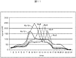
図11は検出電極Rx12から検出電極Rx2方向にスワイプしたときのシグナル値(ΔVb’とΔVa’の差分値)である。横軸の時間の一目盛りはタッチ検出処理の周期である。 FIG. 11 shows a signal value (difference value between ΔVb ′ and ΔVa ′) when swiping from the detection electrode Rx12 toward the detection electrode Rx2. One scale of time on the horizontal axis is the period of the touch detection process.
図12Aおよび図12Bに示すように、表示動作停止状態中に、ドライバIC5内のマイクロコンピュータ(MPU)16は、タッチパネル(TPC)107を擬似ミューチュアル(self)動作させ(ST)、その間(LP)はループしている。マイクロコンピュータ16は、擬似ミューチュアル(self)動作の終了(END)を検出すると、スリープモード(Sleep)になる。スリープモードではタイマカウンタのみが動作し、所定時間が経過すると、マイクロコンピュータ16は次のタッチまたはスワイプの有無を検出するタッチ検出処理を実行する。マイクロコンピュータ16がタッチ検出処理を例えば50ms周期で実行するのが好ましい。
As shown in FIGS. 12A and 12B, during the display operation stop state, the microcomputer (MPU) 16 in the
図12Aに示すように、シングルタッチ起動では、タッチを1回検出すると、マイクロコンピュータ16はホストコントローラ(HOST)200に割込み信号(INT)を出力する。ダブルタッチ起動では、タッチを2回検出すると、マイクロコンピュータ16はホストコントローラ200に割込み信号(INT)を出力する。
ダブルタッチ起動においては、図12Aに示すように、ホストコントローラ200は、割込み信号(INT)を2回受理すると、表示装置100にスリープモード解除信号(Exit sleep)を入力し、表示装置のスリープモードを解除する。表示装置100の駆動回路101はパワーオンシーケンス(P_ON_SQ)を経て表示動作状態(BK、Normal)になる。また駆動回路101は内部リセット信号(RST)を発生してマイクロコンピュータ16に入力し、マイクロコンピュータ16はブート処理(Boot)を経て、タッチパネル(TPC)107をミューチュアル(Mutual)動作させタッチ検出処理(Farmware)を実行する。なお、割込み信号(INT)を1回受理しても、1回受理後に所定時間内(たとえば1秒内)にもう一度割込み信号(INT)を受理しない場合は表示装置100は表示を行わないままとなる。
シングルタッチ起動においては、図示はないが、ホストコントローラ200は、割込み信号(INT)を1回受理すると、表示装置100にスリープモード解除信号(Exit sleep)を入力し、表示装置のスリープモードを解除する。表示装置100の駆動回路101はパワーオンシーケンス(P_ON_SQ)を経て表示動作状態(BK、Normal)になる。また駆動回路101は内部リセット信号(RST)を発生してマイクロコンピュータ16に入力し、マイクロコンピュータ16はブート処理(Boot)を経て、タッチパネル(TPC)107をミューチュアル(Mutual)動作させタッチ検出処理(Farmware)を実行する。
As shown in FIG. 12A, in single touch activation, when a touch is detected once, the
In the double touch activation, as shown in FIG. 12A, when the
In single touch activation, although not shown, when the
図12Bに示すように、スワイプ起動では、タッチを1回検出すると、マイクロコンピュータ16はスリープモードに遷移しないで、連続するタッチを検出し、移動(スワイプ)があったどうかの判定(gesture判定)を行う。マイクロコンピュータ16は、スワイプを検出すると、ホストコントローラ200に割込み信号(INT)を出力する。連続するタッチとは、タッチ検出される箇所がずれつつ所定時間内(たとえば50ms内)に検出されるものである。この所定時間はシングルタッチ起動における所定時間よりもはるかに短くなっている。マイクロコンピュータ16はgesture判定の際に他のループ(LP)よりも長いループとなっており、1回のタッチが検出された後にgesture判定のための長いループとなる。
As shown in FIG. 12B, in the swipe activation, when a touch is detected once, the
図12Aおよび図12Bに示すように、ホストコントローラ200は、割込み信号(INT)を受理すると、表示装置100にスリープモード解除信号(Exit sleep)を入力し、表示装置のスリープモードを解除する。表示装置100の駆動回路はパワーオンシーケンス(P_ON_SQ)を経て表示動作状態(BK、Normal)になる。また駆動回路は内部リセット信号(RST)を発生してマイクロコンピュータ16に入力し、マイクロコンピュータ16はブート処理(Boot)を経て、タッチパネル(TPC)107をミューチュアル(Mutual)動作させタッチ検出処理(Farmware)を実行する。
As shown in FIGS. 12A and 12B, when the
以上説明したように、本実施例では、表示装置100はシングルタッチ起動、またはダブルタッチ起動を行うモードと、スワイプ起動を行うモードの両方を持っており、表示装置100の駆動回路101内のレジスタにホストコントローラ200が所定の値を書き込むことによりこれらモードが実行される。スリープモード時に、CF基板3上に形成される、裏面側透明導電膜(CD)を、帯状のパターンに分割して構成されたタッチパネルの検出電極Rxのみを使用してタッチ検出処理を実行し、表示パネルの表示動作を停止させた状態で、走査電極Txのスキャンを行うことがないので、表示パネルの液晶層に直流電圧が印加され、液晶層に焼き付きが発生するのを防止することが可能となる。
また、本実施例では、スリープモード時に、仮走査電極T’xとして機能する検出電極Rxに接続される積分回路10およびサンプルホールド回路11をOFFとするので、検出回路で消費される電力は半分となるので、スリープモード時の消費電力をより低減することが可能となる。
As described above, in this embodiment, the
In this embodiment, since the
実施例2に係る表示装置について、図13〜図16を用いて以下説明する。
図13は実施例2に係る表示装置の平面図である。
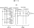
実施例2に係る表示装置は実施例1に係る表示装置とTFT基板内の構成およびドライバICの構成が異なるが、その他の構成は同じである。実施例2に係る表示装置100aは、TFT基板2上に2本の帯状の共通電極(COMMON1、COMMON22)21aと20本の帯状の共通電極(COMMON2〜COMMON21)21bを有する。共通電極の本数が実施例1に係る表示装置100に比べて増加している。その結果、共通電極信号線が増加し、額縁領域の幅も増加する。そこで、表示装置100aは、額縁領域の幅を増大させないように、共通電極の走査回路(Txスキャン回路)23をゲートスキャン回路6と同様にTFT基板2上に形成する。したがって、ドライバIC5aは、ドライバIC5と異なり、Txスキャン回路を有しない。1つの共通電極21aは60ライン分の画素に共通して用いられ、1つの共通電極21bは58ライン分の画素に共通して用いられる。表示装置100aの擬似ミューチュアルにおける走査パルス電圧の極性は、表示装置100の擬似ミューチュアルにおける走査パルス電圧の極性と異なる。上記以外は、表示装置100aは表示装置100と同じである。
A display device according to Example 2 will be described below with reference to FIGS.
FIG. 13 is a plan view of the display device according to the second embodiment.
The display device according to the second embodiment is different from the display device according to the first embodiment in the configuration of the TFT substrate and the configuration of the driver IC, but the other configurations are the same. The
以下、表示装置100aと表示装置100との相違点を説明する。
図14Aは実施例1のTx同相駆動の模式図である。図14Bは実施例2のTx差動駆動(1)の模式図である。図14Cは実施例2のTx差動駆動(2)の模式図である。図14Dは実施例2のTx差動駆動(3)の模式図である。
実施例1では、図14Aに示すように、仮走査電極Tx’(検出電極Rx1、Rx3、Rx5、Rx7、Rx9、Rx11、言い換えると奇数番目の検出電極Rx_Odd)は、同極性(例えば、すべて正極性)の走査パルス電圧(VQTX)で駆動される。図14Aに示される駆動を同相駆動ともいう。
一方、実施例2では、図14B、図14C、図14Dに示すように、仮走査電極Tx’(検出電極Rx1、Rx3、Rx5、Rx7、Rx9、Rx11、言い換えると奇数番目の検出電極Rx_Odd)は、異極性の走査パルス電圧(VQTX(+)、VQTX(−))で駆動される。図14B、図14C、図14Dに示される駆動を差動駆動ともいう。
Hereinafter, differences between the
FIG. 14A is a schematic diagram of Tx in-phase driving according to the first embodiment. FIG. 14B is a schematic diagram of Tx differential driving (1) according to the second embodiment. FIG. 14C is a schematic diagram of Tx differential driving (2) according to the second embodiment. FIG. 14D is a schematic diagram of Tx differential driving (3) according to the second embodiment.
In Example 1, as shown in FIG. 14A, the temporary scanning electrodes Tx ′ (detection electrodes Rx1, Rx3, Rx5, Rx7, Rx9, Rx11, in other words, odd-numbered detection electrodes Rx_Odd) have the same polarity (for example, all positive electrodes Driven by a scanning pulse voltage (V QTX ). The drive shown in FIG. 14A is also referred to as in-phase drive.
On the other hand, in the second embodiment, as shown in FIGS. 14B, 14C, and 14D, the provisional scan electrode Tx ′ (detection electrodes Rx1, Rx3, Rx5, Rx7, Rx9, Rx11, in other words, the odd-numbered detection electrode Rx_Odd) Are driven by scanning pulse voltages of different polarities (V QTX (+), V QTX (−)). The driving shown in FIGS. 14B, 14C, and 14D is also referred to as differential driving.
図14Bに示すように、第1のTx差動駆動では、検出電極Rx1、Rx5、Rx9は正極性の走査パルス電圧(VQTX(+))、検出電極Rx3、Rx7、Rx11は負極性の走査パルス電圧(VQTX(−))で駆動される。すなわち、隣接する仮走査電極Tx’の極性が異なる。
実施例2では、図14Cに示すように、第2のTx差動駆動では、検出電極Rx3、Rx5、Rx11は正極性の走査パルス電圧(VQTX(+))、検出電極Rx1、Rx7、Rx9は負極性の走査パルス電圧(VQTX(−))で駆動される。すなわち、隣接する2つの仮走査電極Tx’は正極性の走査パルス電圧(VQTX(+))で、次の隣接する2つの仮走査電極Tx’は負極性の走査パルス電圧(VQTX(−))で駆動される。
実施例2では、図14Dに示すように、第3のTx差動駆動では、検出電極Rx1、Rx3、Rx5は正極性の走査パルス電圧(VQTX(+))、検出電極Rx7、Rx9、Rx11は負極性の走査パルス電圧(VQTX(−))で駆動される。すなわち、半分の隣接する仮走査電極Tx’は正極性の走査パルス電圧(VQTX(+))で、残りの半分の隣接する仮走査電極Tx’は負極性の走査パルス電圧(VQTX(−))で駆動される。
As shown in FIG. 14B, in the first Tx differential drive, the detection electrodes Rx1, Rx5, and Rx9 have a positive scan pulse voltage (V QTX (+)), and the detection electrodes Rx3, Rx7, and Rx11 have a negative scan. It is driven by a pulse voltage (V QTX (−)). That is, the polarities of the adjacent temporary scan electrodes Tx ′ are different.
In the second embodiment, as shown in FIG. 14C, in the second Tx differential drive, the detection electrodes Rx3, Rx5, and Rx11 have the positive scanning pulse voltage (V QTX (+)), the detection electrodes Rx1, Rx7, and Rx9. Are driven by a negative scan pulse voltage (V QTX (−)). That is, two adjacent temporary scan electrodes Tx ′ have a positive scan pulse voltage (V QTX (+)), and the next two adjacent temporary scan electrodes Tx ′ have a negative scan pulse voltage (V QTX (−). )).
In the second embodiment, as shown in FIG. 14D, in the third Tx differential drive, the detection electrodes Rx1, Rx3, and Rx5 are positive scan pulse voltages (V QTX (+)), the detection electrodes Rx7, Rx9, and Rx11. Are driven by a negative scan pulse voltage (V QTX (−)). That is, half of the adjacent temporary scan electrodes Tx ′ have a positive scan pulse voltage (V QTX (+)), and the other half of the adjacent temporary scan electrodes Tx ′ have a negative scan pulse voltage (V QTX (−). )).
以下、図15Aおよび図15Bを用いて、疑似ミューチュアル検出時の検出回路108aの動作を説明する。
図15Aは実施例2に係る検出回路における、表示動作停止中の動作を説明するための図である。図15Bは実施例2に係る検出回路における、表示動作停止中のタッチパネルのタッチ検出動作のタイミング図である。図16は実施例2に係る検出回路のスワイプ操作におけるタッチ信号変化を示す図である。
Hereinafter, the operation of the
FIG. 15A is a diagram for explaining the operation of the detection circuit according to the second embodiment when the display operation is stopped. FIG. 15B is a timing diagram of the touch detection operation of the touch panel while the display operation is stopped in the detection circuit according to the second embodiment. FIG. 16 is a diagram illustrating a touch signal change in the swipe operation of the detection circuit according to the second embodiment.
実施例2に係る検出回路108aと実施例1に係る検出回路108とは回路構成は同じである。ただし、検出回路108aのキャリブレーションアンプ17に印加される電圧と検出回路108のキャリブレーションアンプ17に印加される電圧とが異なる。すなわち、走査パルス電圧(VQTX)およびキャリブレーションパルス電圧(VCLB)が異なる。
The
(1)検出電極および積分回路のリセット
スイッチS2_ODDとスイッチS3_ODDをOFFし、スイッチS7_ODDをONして、検出電極Rx_Odd(+)、Rx_Odd(−)を仮走査電極T’xとして使用できるようにする。また、検出電極Rx_Odd(+)に係るスイッチS5_ODDは、VDAC側(VDAC=0.25V)に接続されており、走査パルス電圧(VQTX(+)=0.25V)を出力し、検出電極Rx_Oddは0.25Vにリセットされる。検出電極Rx_Odd(−)に係るスイッチS5_ODDは、VCLB側(VCLB=4V)に接続されており、走査パルス電圧(VQTX(−)=4V)を出力し、検出電極Rx_Oddは4Vにリセットされる。
各検出電極Rx_Evenに流れる電流を検出(積分)前に、スイッチS2_EVEN、スイッチS4_EVEN、スイッチS7_EVENをOFFし、スイッチS1_EVENをONして、積分回路10をリセットするとともに、スイッチS3_EVENをONとして、各検出電極Rx_Evenをリセットする。
基準電圧(VREF)を4V(VREF=4V)とすると、積分回路10の出力は4V、各検出電極Rx_Evenは、4Vにプリチャージされる。
また、スイッチS5_EVENは、VOFSC側(VOFSC=2.118V)に接続されており、キャリブレーション容量Cclbの両端には、4V−2.118Vの電圧が印加される。
(1) Detection electrode and integration circuit reset Switch S2_ODD and switch S3_ODD are turned OFF and switch S7_ODD is turned ON so that detection electrodes Rx_Odd (+) and Rx_Odd (−) can be used as temporary scanning electrodes T′x. . The switch S5_ODD related to the detection electrode Rx_Odd (+) is connected to the V DAC side (V DAC = 0.25V ), and outputs a scan pulse voltage (V QTX (+) = 0.25V ) for detection. The electrode Rx_Odd is reset to 0.25V. The switch S5_ODD related to the detection electrode Rx_Odd (−) is connected to the V CLB side (V CLB = 4V), outputs a scanning pulse voltage (V QTX (−) = 4V), and the detection electrode Rx_Odd is reset to 4V. Is done.
Before detecting (integrating) the current flowing through each detection electrode Rx_Even, the switch S2_EVEN, the switch S4_EVEN, and the switch S7_EVEN are turned off, the switch S1_EVEN is turned on, the
Assuming that the reference voltage (V REF ) is 4V (V REF = 4V), the output of the integrating
The switch S5_EVEN is connected to the V OFSC side (V OFSC = 2.118V), and a voltage of 4V-2.118V is applied to both ends of the calibration capacitor Cclb.
(2)積分
次に、スイッチS1_EVENとスイッチS3_EVENをOFFとした後、検出電極Rx_Odd(+)に係るスイッチスイッチS5_ODDは、VOFSC側(VOFSC=2.118V)に接続され、検出電極Rx_Odd(+)に走査パルス電圧(VQTX(+)=2.118V)を出力する。検出電極Rx_Odd(−)に係るスイッチスイッチS5_ODDは、VOFSC側(VOFSC=2.118V)に接続され、検出電極Rx_Odd(−)に走査パルス電圧(VQTX(−)=2.118V)を出力する。スイッチS5_EVENはVDAC側(VDAC=0.25〜4V)に切り替え、キャリブレーション容量Cclbの一端に、キャリブレーションパルス電圧(VCLB)を印加し、交差容量Cxyの電荷の引き抜きを行った後に、スイッチS2_EVENをONとして残りの電荷を積分容量Cintに積分する。
これにより、検出電極Rx_Evenの1つを、検出容量Crx−rx、積分容量Cintの経路で電流が流れ、積分回路10の出力電圧(VINT)が低下する。
(2) Integration Next, after turning off the switch S1_EVEN and the switch S3_EVEN, the switch switch S5_ODD related to the detection electrode Rx_Odd (+) is connected to the V OFSC side (V OFSC = 2.118V), and the detection electrode Rx_Odd ( The scanning pulse voltage (V QTX (+) = 2.118 V) is output to (+). The switch S5_ODD related to the detection electrode Rx_Odd (−) is connected to the V OFSC side (V OFSC = 2.118V), and the scan pulse voltage (V QTX (−) = 2.118V) is applied to the detection electrode Rx_Odd (−). Output. The switch S5_EVEN is switched to the V DAC side (V DAC = 0.25 to 4 V), the calibration pulse voltage (V CLB ) is applied to one end of the calibration capacitor Cclb, and the charge of the cross capacitor Cxy is extracted. Then, the switch S2_EVEN is turned on to integrate the remaining charge into the integration capacitor Cint.
As a result, a current flows through one of the detection electrodes Rx_Even through the path of the detection capacitor Crx-rx and the integration capacitor Cint, and the output voltage (V INT ) of the
(3)検出電極のリセット
積分回路10での積分終了後、検出電極Rx_Odd(+)に係るスイッチS5_ODDは、VDAC側(VDAC=0.25V)に接続されており、走査パルス電圧(VQTX(+)=0.25V)を出力し、検出電極Rx_Odd(+)は0.25Vにリセットされる。検出電極Rx_Odd(−)に係るスイッチS5_ODDは、VDAC側(VDAC=4V)に接続されており、走査パルス電圧(VQTX(−)=4V)を出力し、検出電極Rx_Odd(−)は4Vにリセットされる。スイッチS2_EVENをOFF、スイッチS3_EVENをONとして、スイッチS5_EVENは、VOFSC側(VOFSC=2.118V)に接続して、各検出電極Rx_Evenを4Vにプリチャージするとともに、キャリブレーション容量Cclbに1.882V(=4V−2.118V)の電圧が印加される。
(3) Detection electrode reset After the integration in the
(4)上記(2)の積分回路10での積分動作を繰り返し、電圧を積み上げる。
(4) The integration operation in the
(5)積分回路10での積分完了後、スイッチS4_EVENをONとして、サンプルホールド回路11でサンプル&ホールドし、その後、スイッチS6_EVENを順次ONとして、AD変換器12でAD変換し、メモリ(RAM)13に、偶数番目の検出電極Rx_Even分のRAWデータを格納する。
AD変換器12が、10bitのAD変換器の場合、RAWデータは0(積分0V)〜1023(積分4V)の範囲となる。
(5) After the integration in the
When the
(6)上記(1)〜(5)の処理を、全ての偶数番目の検出電極Rx_Evenについて順次実行し、各偶数番目の検出電極Rx_Evenと各奇数番目の検出電極Rx_Oddの隣接1面分のRAWデータをメモリ13に格納する。
(6) The processes of (1) to (5) are sequentially executed for all even-numbered detection electrodes Rx_Even, and RAW for one adjacent surface of each even-numbered detection electrode Rx_Even and each odd-numbered detection electrode Rx_Odd. Data is stored in the
(7)検出容量Crx−rxの容量値は非タッチ時の方がタッチ時よりも大きいので、積分回路10での出力電圧(VINT)の降下に差が生じ、ここにしきい値を設けて、タッチまたはスワイプの有無を検出する。
(7) Since the capacitance value of the detection capacitance Crx-rx is larger when not touching than when touching, there is a difference in the drop of the output voltage (V INT ) in the
タッチ部によって検出信号が上下方向に出力するため、図15Bに示すように10bitのAD変換器の中間値(RAWデータ=511)をキャリブレーション目標値(VCLBT)としている。図15Aの(A)側をタッチしたときは、積分回路10の出力電圧(VINT)はキャリブレーション目標値よりも高い電圧(VINT(A))になる。図15Aの(B)側をタッチしたときは、積分回路10の出力電圧(VINT)はキャリブレーション目標値よりも低い電圧(VINT(B))になる。
Since the detection signal is output in the vertical direction by the touch unit, as shown in FIG. 15B, the intermediate value (RAW data = 511) of the 10-bit AD converter is set as the calibration target value (V CLBT ). When the (A) side in FIG. 15A is touched, the output voltage (V INT ) of the
図16は第3のTx差動駆動における検出電極Rx12から検出電極Rx2方向にスワイプしたときのシグナル値である。横軸の時間の一目盛りはタッチ検出処理の周期である。検出電極Rx2、Rx4、Rx6は正のシグナル値で、検出電極Rx8、Rx10、Rx12は負のシグナル値である。 FIG. 16 shows signal values when swiping from the detection electrode Rx12 to the detection electrode Rx2 in the third Tx differential drive. One scale of time on the horizontal axis is the period of the touch detection process. The detection electrodes Rx2, Rx4, and Rx6 have positive signal values, and the detection electrodes Rx8, Rx10, and Rx12 have negative signal values.
図17Aは実施例2に係るTxスキャン回路の構成を示すブロック図である。図17Bは実施例2に係るTxスキャン回路のスイッチ回路の回路図である。図18AはRx積分量変化の模式図である。図18BはRx積分量変化の波形図である。図18CはTx差動駆動による改善模式図である。 FIG. 17A is a block diagram illustrating the configuration of the Tx scan circuit according to the second embodiment. FIG. 17B is a circuit diagram of the switch circuit of the Tx scan circuit according to the second embodiment. FIG. 18A is a schematic diagram of a change in Rx integration amount. FIG. 18B is a waveform diagram of a change in Rx integration amount. FIG. 18C is a schematic diagram of improvement by Tx differential driving.
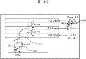
Txスキャン回路23は、スイッチ回路TxSWとシフトレジスタ回路TxS/Rから構成される。スイッチ回路TxSWは、図17Bに示されるように、nチャネルTFTと容量で構成される。スリープモードになるときは、SD_RST信号がHighとなり、薄膜トランジスタT12を介して薄膜トランジスタT19はONし、容量C2は充電される。続くパワーオフシーケンス後、入力信号の各ノードはすべてGND電位に固定される。薄膜トランジスタT10、T13のリーク電流により、容量C2が徐々に放電する。薄膜トランジスタT19がONからオープンに遷移することで、薄膜トランジスタT19のON抵抗が変化する。図18Aに示すように(a)リーク電流により薄膜トランジスタT19のON抵抗が変化すると、(b)検出電極Rx_EvenとGND間のインピーダンスが変化する。(c)その結果、仮走査電極(検出電極R_Odd)への走査パルスによって、検出容量Crx−rxの積分容量Cintとセルフ容量Crx−gndへの電荷配分が変化し、(d)積分容量Cintの積分電荷量(Qint)が変化する。なお、薄膜トランジスタのリーク電流は光や温度、Vthに依存する。
The
図18Bに示すように、スリープモードの初期期間(i)は、薄膜トランジスタT19がONで安定している。したがって、積分容量Cintの積分電荷量(Qint)が変化しないので、感度は低いがスワイプ検出は可能である。過渡期間(ii)は、上述したように、ON抵抗が変化し、積分電荷量(Qint)が変化するので、スワイプ検出は困難である。安定期間(iii)は、放電しきっているのでリーク電流がほとんどなく、ON抵抗はオープン状態でほとんど変化しない。したがって、積分電荷量(Qint)が変化しないので、スワイプ検出は可能である。なお、薄膜トランジスタのリーク電流は光や温度、Vthに依存し、早くリークする条件においては、過渡期間(ii)の期間が短くなるので、スワイプ検出が不可能な期間は短くなる。 As shown in FIG. 18B, in the initial period (i) of the sleep mode, the thin film transistor T19 is ON and is stable. Therefore, since the integral charge amount (Qint) of the integral capacitor Cint does not change, swipe detection is possible although the sensitivity is low. In the transient period (ii), as described above, the ON resistance changes and the integrated charge amount (Qint) changes, so that swipe detection is difficult. During the stable period (iii), since the discharge is completed, there is almost no leakage current, and the ON resistance hardly changes in the open state. Therefore, since the integrated charge amount (Qint) does not change, swipe detection is possible. Note that the leakage current of the thin film transistor depends on light, temperature, and Vth. Under the condition of early leakage, the period of the transient period (ii) is shortened, so that the period during which swipe detection is impossible is shortened.
実施例2では、TFTを用いてTxスキャン回路23をTFT基板2上に形成しているため、上記のような問題が発生する可能性がある。しかし、実施例2では、図18Cに示すように、仮走査電極(検出電極Rx_Odd)はVQTX(+)とVQTX(−)とによって差動駆動される。したがって、図18Bと同様に、(a)リーク電流により薄膜トランジスタT19のON抵抗が変化し、(b)検出電極Rx_EvenとGND間のインピーダンスが変化しても、走査パルスがバランスするため、(c)仮走査電極(検出電極R_Odd)への走査パルスによる電荷がセルフ容量Crx−gndに抜けがなくなる。したがって、(d)積分容量Cintの容量値(CINT)が安定する。すなわち、仮走査電極(検出電極R_Odd)への走査パルスがバランスするため、検出電極Rx_EvenとGND間のインピーダンスが変化を見えなくすることができる。
In the second embodiment, since the
1・・・表示パネル
2・・・TFT基板(アレイ基板)
3・・・CF基板(対向基板)
4・・・液晶層
5、5a・・・ドライバIC
6・・・ゲートスキャン回路
7・・・走査信号線
8・・・映像信号線
9・・・ドライバIC用入力端子
10・・・積分回路
11・・・サンプルホールド回路
12・・・AD変換器(ADC)
13・・・メモリ(RAM)
14・・・メモリ(RAM)
15・・・DA変換器(DAC)
16・・・マイクロコンピュータ(MPU)
17・・・キャリブレーションアンプ
20・・・画素部
21、21a、21b・・・共通電極(対向電極、走査電極)
22・・・共通電極信号線
23・・・Txスキャン回路
31・・・検出電極
40・・・フロントウィンドウ(又は保護フィルム)
70、75・・・フレキシブル配線基板
77・・・接続部
80・・・コネクタ
100・・・表示装置
101・・・駆動回路
102・・・シーケンサ
103・・・走査パルス電圧生成回路
106・・・デコーダ回路
107・・・タッチパネル
108・・・検出回路
200・・・ホストコントローラ
BKL・・・バックライト
Cclb・・・キャリブレーション容量
Cint・・・積分容量
Crx−rx・・・検出容量
Cxy・・・交差容量
LC・・・液晶層
POL1、POL2・・・偏光板
Rx・・・タッチパネルの検出電極
Tx・・・タッチパネルの走査電極
T’x・・・表示動作停止時の走査電極
1.
3 ... CF substrate (counter substrate)
4 ...
6 ...
13 ... Memory (RAM)
14 ... Memory (RAM)
15 ... DA converter (DAC)
16 ... Microcomputer (MPU)
17 ...
22 ... Common
70, 75 ...
Claims (20)
対向基板と、
検出回路と、
を備える表示装置であって、
前記表示装置は、第1のモードと、第2のモードと、を有し、
前記アレイ基板は、画素電極と、共通電極と、を有し、
前記対向基板は、第1の検出電極と、第2の検出電極と、を有し、
前記第1の検出電極は、前記第2の検出電極と交互に配置され、
前記第1のモードでは、
前記共通電極は、表示の電極とタッチパネルの走査電極を兼用するようにされ、コモン電圧と第1の走査パルス電圧とが供給され、
前記検出回路は、前記第1および第2の検出電極で検出される検出電圧に基づきタッチ位置を検出するようにされ、
前記第2のモードでは、
前記第1の検出電極は仮走査電極として機能させられ、
前記検出回路は、前記第1の検出電極に第2の走査パルス電圧を供給するようにされ、前記第2の検出電極で検出される検出電圧に基づき検出対象の移動の有無を検出するようにされる表示装置。 And the array substrate,
A counter substrate;
A detection circuit;
A Ru display device comprising a,
The display device has a first mode and a second mode,
The array substrate has a pixel electrode and a common electrode,
The counter substrate has a first detection electrode and a second detection electrode,
The first detection electrodes are alternately arranged with the second detection electrodes,
In the first mode,
The common electrode is used as a display electrode and a scan electrode of a touch panel, and a common voltage and a first scan pulse voltage are supplied.
The detection circuit detects a touch position based on a detection voltage detected by the first and second detection electrodes,
In the second mode,
The first detection electrode is caused to function as a temporary scanning electrode;
The detection circuit is configured to supply a second scanning pulse voltage to the first detection electrode, and detect the presence or absence of movement of the detection target based on the detection voltage detected by the second detection electrode. Display device .
前記第1の検出電極は、前記第2の検出電極を挟んで、第3の検出電極と、第4の検出電極とに分類され、
前記第2のモード時に、前記検出回路は、前記第3の検出電極と前記第4の検出電極とに前記第2の走査パルス電圧を同極性のパルスで複数回供給するようにされる表示装置。 Oite to claim 1,
The first detection electrode is classified into a third detection electrode and a fourth detection electrode across the second detection electrode ,
Wherein the second mode, the detection circuit, the third detection electrode and the fourth is the on the detected electrode and the second scan pulse voltage so as to supply a plurality of times with the same polarity pulse display device .
前記第2の走査パルス電圧は正極性のパルスである表示装置。 Oite to claim 2,
The display device, wherein the second scanning pulse voltage is a positive pulse.
前記第1の検出電極は、前記第2の検出電極を挟んで、第3の検出電極と、第4の検出電極とに分類され、
前記第2のモード時に、前記検出回路は、前記第3の検出電極と前記第4の検出電極とに前記第2の走査パルス電圧を異極性のパルスで複数回供給するようにされる表示装置。 Oite to claim 1,
The first detection electrode is classified into a third detection electrode and a fourth detection electrode across the second detection electrode ,
Wherein the second mode, the detection circuit, the third detection electrode and the fourth the to the detection electrode a second scan pulse voltage is to be supplied several times in opposite polarity of the pulse display device .
前記検出回路は、前記第1の検出電極に接続される第1のスイッチ回路を有し、
前記第2のモード時に、前記第1のスイッチ回路がオンとなり、前記第1の検出電極に前記第2の走査パルス電圧を供給するようにされる表示装置。 Oite to claim 1,
The detection circuit has a first switch circuit connected to the first detection electrode;
Wherein the second mode, the first switch circuit is turned on, a display device which is adapted to supply the second scan pulse voltage to the first sensing electrode.
前記検出回路は、前記第1の検出電極に接続される第2のスイッチ回路と、前記第2のスイッチ回路に接続される積分回路とを有し、
前記第1のモード時にタッチを検出するときは、前記積分回路は、前記第2スイッチ回路を介して、前記第1の検出電極に接続され、
前記第2のモード時は、前記第2スイッチ回路はオフされ、前記積分回路はオフされる表示装置。 Oite to claim 1,
The detection circuit includes a second switch circuit connected to the first detection electrode, and an integration circuit connected to the second switch circuit,
When detecting a touch in the first mode, the integration circuit is connected to the first detection electrode via the second switch circuit;
The second mode, the second switch circuit is turned off, the integrating circuit display device is turned off.
前記共通電極は、複数のブロックに分割されており、
前記分割された各ブロックの共通電極は、連続する複数の表示ラインの各画素に対して共通に設けられる表示装置。 Oite to claim 1,
The common electrode is divided into a plurality of blocks;
The display device in which the common electrode of each of the divided blocks is provided in common for each pixel of a plurality of continuous display lines.
前記第2のモード時に、前記分割された各ブロックの共通電極は、基準電位に固定される表示装置。 Oite to claim 7,
The display device in which the common electrode of each of the divided blocks is fixed to a reference potential in the second mode.
前記検出電極は、ストライプ形状で、第1方向に延在し、
前記分割された各ブロックの共通電極は、ストライプ形状で、前記第1方向とは異なる第2方向に延在する表示装置。 Oite to claim 7,
The detection electrode has a stripe shape and extends in the first direction;
The display device in which the common electrode of each of the divided blocks has a stripe shape and extends in a second direction different from the first direction.
前記アレイ基板と前記対向基板との間に狭持される液晶を有する表示装置。 Oite to claim 1,
A display device having a liquid crystal sandwiched between the array substrate and the counter substrate.
前記検出回路は、第2の走査パルス電圧を生成するためのレジスタおよびキャリブレーション電圧を生成するためのメモリを有する表示装置。 Oite to claim 1,
Wherein the detection circuit includes a display device having a memory for generating the registers and the calibration voltage for generating a second scan pulse voltage.
対向基板と、
前記アレイ基板と前記対向基板との間に狭持される液晶と、
検出回路と、
を備える表示装置であって、
前記表示装置は、第1のモードと、第2のモードと、を有し、
前記アレイ基板は、画素電極と、共通電極と、を有し、
前記対向基板は、第1の検出電極と、第2の検出電極と、を有し、
前記第1の検出電極は、前記第2の検出電極と交互に配置され、
前記検出回路は、積分回路と、前記積分回路用のキャリブレーション電圧を供給する電圧供給回路を有し、
前記第1のモードでは、
前記共通電極は、表示の電極とタッチパネルの走査電極を兼用するようにされ、コモン電圧と第1の走査パルス電圧とが供給され、
前記検出回路は、前記第1および第2の検出電極で検出される検出電圧に基づきタッチ位置を検出するようにされ、
前記第2のモードでは、
前記第1の検出電極は仮走査電極として機能させられ、
前記電圧供給回路は、前記第1の検出電極に第2の走査パルス電圧を供給するようにされ、
前記検出回路は、前記第2の検出電極で検出される検出電圧に基づきタッチまたは検出対象の移動の有無を検出するようにされる表示装置。 And the array substrate,
A counter substrate;
A liquid crystal sandwiched between the array substrate and the counter substrate;
A detection circuit;
A Ru display device comprising a,
The display device has a first mode and a second mode,
The array substrate has a pixel electrode and a common electrode,
The counter substrate has a first detection electrode and a second detection electrode,
The first detection electrodes are alternately arranged with the second detection electrodes,
The detection circuit includes an integration circuit and a voltage supply circuit that supplies a calibration voltage for the integration circuit,
In the first mode,
The common electrode is used as a display electrode and a scan electrode of a touch panel, and a common voltage and a first scan pulse voltage are supplied.
The detection circuit detects a touch position based on a detection voltage detected by the first and second detection electrodes,
In the second mode,
The first detection electrode is caused to function as a temporary scanning electrode;
The voltage supply circuit is configured to supply a second scan pulse voltage to the first detection electrode;
The display device is configured to detect the presence or absence of touch or movement of a detection target based on a detection voltage detected by the second detection electrode.
前記第1の検出電極は、前記第2の検出電極を挟んで、第3の検出電極と、第4の検出電極とに分類され、
前記第2のモード時に、前記電圧供給回路は、前記第3の検出電極と前記第4の検出電極とに前記第2の走査パルス電圧を同極性のパルスで複数回供給するようにされる表示装置。 Oite to claim 1 2,
The first detection electrode is classified into a third detection electrode and a fourth detection electrode across the second detection electrode ,
Wherein the second mode display, the voltage supply circuit, which is the third detection electrode and the second scan pulse voltage and fourth detection electrodes to supply a plurality of times with the same polarity pulse Equipment .
前記第2の走査パルス電圧は正極性のパルスである表示装置。 In claim 13,
The display device, wherein the second scanning pulse voltage is a positive pulse.
前記第1の検出電極は、前記第2の検出電極を挟んで、第3の検出電極と、第4の検出電極とに分類され、
前記第2のモード時に、前記電圧供給回路は、前記第3の検出電極と前記第4の検出電極とに前記第2の走査パルス電圧を異極性のパルスで複数回供給するようにされる表示装置。 Oite to claim 1 2,
The first detection electrode is classified into a third detection electrode and a fourth detection electrode across the second detection electrode ,
Wherein the second mode display, the voltage supply circuit, which is the third detection electrode and the second scan pulse voltage and fourth detection electrodes to supply a plurality of times in different polarity pulse Equipment .
前記検出回路は、前記第1の検出電極と前記電圧供給回路を接続する第1のスイッチ回路を有し、
前記第2のモード時に、前記第1のスイッチ回路がオンとなり、前記電圧供給回路は前記第1の検出電極に前記第2の走査パルス電圧を供給するようにされる表示装置。 Oite to claim 1 2,
The detection circuit includes a first switch circuit that connects the first detection electrode and the voltage supply circuit;
Wherein the second mode, the first switch circuit is turned on, the voltage supply circuit is a display device which is adapted to supply the second scan pulse voltage to the first sensing electrode.
前記検出回路は、前記第1の検出電極と前記積分回路を接続する第2のスイッチ回路を有し、
前記第1のモード時にタッチを検出するときは、前記積分回路は、前記第2スイッチ回路を介して、前記第1の検出電極に接続され、
前記第2のモード時は、前記第2スイッチ回路はオフされ、前記積分回路はオフされる表示装置。 Oite to claim 1 2,
The detection circuit includes a second switch circuit that connects the first detection electrode and the integration circuit;
When detecting a touch in the first mode, the integration circuit is connected to the first detection electrode via the second switch circuit;
The second mode, the second switch circuit is turned off, the integrating circuit display device is turned off.
前記共通電極は、複数のブロックに分割されており、
前記分割された各ブロックの共通電極は、連続する複数の表示ラインの各画素に対して共通に設けられる表示装置。 Oite to claim 1 2,
The common electrode is divided into a plurality of blocks;
The display device in which the common electrode of each of the divided blocks is provided in common for each pixel of a plurality of continuous display lines.
前記第2のモード時に、前記分割された各ブロックの共通電極は、基準電位に固定される表示装置。 Oite to claim 1 8,
The display device in which the common electrode of each of the divided blocks is fixed to a reference potential in the second mode.
前記検出電極は、ストライプ形状で、第1方向に延在し、
前記分割された各ブロックの共通電極は、ストライプ形状で、前記第1方向とは異なる第2方向に延在する表示装置。 Oite to claim 1 8,
The detection electrode has a stripe shape and extends in the first direction;
The display device in which the common electrode of each of the divided blocks has a stripe shape and extends in a second direction different from the first direction.
Priority Applications (5)
| Application Number | Priority Date | Filing Date | Title |
|---|---|---|---|
| JP2013254209A JP6211409B2 (en) | 2013-12-09 | 2013-12-09 | Display device |
| US14/564,125 US9317169B2 (en) | 2013-12-09 | 2014-12-09 | Display device |
| US15/070,404 US9436314B2 (en) | 2013-12-09 | 2016-03-15 | Display device |
| US15/229,784 US9740329B2 (en) | 2013-12-09 | 2016-08-05 | Display device |
| US15/645,177 US9874971B2 (en) | 2013-12-09 | 2017-07-10 | Display device |
Applications Claiming Priority (1)
| Application Number | Priority Date | Filing Date | Title |
|---|---|---|---|
| JP2013254209A JP6211409B2 (en) | 2013-12-09 | 2013-12-09 | Display device |
Publications (3)
| Publication Number | Publication Date |
|---|---|
| JP2015114704A JP2015114704A (en) | 2015-06-22 |
| JP2015114704A5 JP2015114704A5 (en) | 2017-01-12 |
| JP6211409B2 true JP6211409B2 (en) | 2017-10-11 |
Family
ID=53271783
Family Applications (1)
| Application Number | Title | Priority Date | Filing Date |
|---|---|---|---|
| JP2013254209A Active JP6211409B2 (en) | 2013-12-09 | 2013-12-09 | Display device |
Country Status (2)
| Country | Link |
|---|---|
| US (4) | US9317169B2 (en) |
| JP (1) | JP6211409B2 (en) |
Families Citing this family (21)
| Publication number | Priority date | Publication date | Assignee | Title |
|---|---|---|---|---|
| KR102112528B1 (en) * | 2013-12-10 | 2020-05-19 | 엘지디스플레이 주식회사 | Display device and method of driving the same |
| JP2015232602A (en) * | 2014-06-09 | 2015-12-24 | 株式会社ジャパンディスプレイ | Display device |
| TWI543056B (en) * | 2014-08-14 | 2016-07-21 | 群創光電股份有限公司 | Display apparatus and touch display apparatus |
| KR102278506B1 (en) * | 2014-10-01 | 2021-07-16 | 삼성디스플레이 주식회사 | Display device and driving method thereof |
| JP6480749B2 (en) * | 2015-02-16 | 2019-03-13 | 株式会社ジャパンディスプレイ | Display device |
| CN104679376B (en) * | 2015-03-24 | 2017-07-28 | 京东方科技集团股份有限公司 | A kind of embedded capacitance touch display screen, display panel and display device |
| CN104777936B (en) * | 2015-04-16 | 2016-08-24 | 京东方科技集团股份有限公司 | Touch-control driver element and circuit, display floater and display device |
| CN104882092B (en) * | 2015-06-29 | 2017-12-08 | 京东方科技集团股份有限公司 | A kind of embedded touch display screen and its driving method, display device |
| US10365751B2 (en) * | 2015-07-10 | 2019-07-30 | Tpk Touch Solutions (Xiamen) Inc. | Display device with three-dimension input module |
| US10068121B2 (en) * | 2015-08-31 | 2018-09-04 | Cypress Semiconductor Corporation | Baseline compensation for capacitive sensing |
| CN105301429B (en) * | 2015-11-05 | 2018-05-29 | 深圳市华星光电技术有限公司 | The defects of self-capacitance touch panel detection device and detection method |
| CN106814836A (en) * | 2015-11-30 | 2017-06-09 | 鸿富锦精密工业(深圳)有限公司 | Power-economizing method and the electronic installation using the power-economizing method |
| CN106775143B (en) * | 2015-12-31 | 2020-01-03 | 深圳市汇顶科技股份有限公司 | Integrating circuit and capacitance sensing circuit |
| TWI584172B (en) * | 2016-03-02 | 2017-05-21 | 聯陽半導體股份有限公司 | Touch detection method |
| JP2017167426A (en) * | 2016-03-17 | 2017-09-21 | セイコーエプソン株式会社 | Electronic optical device, and electronic instrument |
| US10282042B2 (en) * | 2016-05-26 | 2019-05-07 | Solomon Systech Limited | Method and apparatus for reducing pin count in in-cell touch display driver IC |
| KR102555827B1 (en) * | 2016-08-31 | 2023-07-17 | 엘지디스플레이 주식회사 | Touch-Type Display Device |
| TWI613640B (en) * | 2017-02-24 | 2018-02-01 | 友達光電股份有限公司 | Touch display apparatus |
| CN107656661A (en) * | 2017-09-26 | 2018-02-02 | 武汉华星光电技术有限公司 | Mutual capacitance touch display panel with fingerprint and liquid crystal display |
| CN109445635B (en) * | 2018-10-31 | 2022-04-01 | 维沃移动通信有限公司 | Mobile terminal and control method thereof |
| CN111443530A (en) * | 2020-04-15 | 2020-07-24 | 深圳市华星光电半导体显示技术有限公司 | Display screen and display device |
Family Cites Families (9)
| Publication number | Priority date | Publication date | Assignee | Title |
|---|---|---|---|---|
| JP5481040B2 (en) | 2008-04-11 | 2014-04-23 | 株式会社ジャパンディスプレイ | Display device and driving method thereof |
| TWI434207B (en) * | 2010-03-25 | 2014-04-11 | Novatek Microelectronics Corp | Touch sensing system, electronic touch apparatus, and touch sensing method |
| JP5458443B2 (en) * | 2010-09-14 | 2014-04-02 | 株式会社ジャパンディスプレイ | Display device with touch detection function and electronic device |
| CN103250350A (en) * | 2010-11-30 | 2013-08-14 | 瑟克公司 | Linear projected single-layer capacitance sensor |
| JP5726111B2 (en) * | 2012-03-14 | 2015-05-27 | 株式会社ジャパンディスプレイ | Image display device |
| JP2013232162A (en) * | 2012-05-01 | 2013-11-14 | Japan Display Inc | Liquid crystal display device with touch panel |
| JP5923417B2 (en) * | 2012-09-14 | 2016-05-24 | 株式会社ジャパンディスプレイ | Display device and cover member |
| JP2014056222A (en) * | 2012-09-14 | 2014-03-27 | Japan Display Inc | Display device and cover member |
| WO2014061261A1 (en) * | 2012-10-15 | 2014-04-24 | パナソニック株式会社 | Input device and liquid crystal display device |
-
2013
- 2013-12-09 JP JP2013254209A patent/JP6211409B2/en active Active
-
2014
- 2014-12-09 US US14/564,125 patent/US9317169B2/en active Active
-
2016
- 2016-03-15 US US15/070,404 patent/US9436314B2/en active Active
- 2016-08-05 US US15/229,784 patent/US9740329B2/en active Active
-
2017
- 2017-07-10 US US15/645,177 patent/US9874971B2/en active Active
Also Published As
| Publication number | Publication date |
|---|---|
| US20170308231A1 (en) | 2017-10-26 |
| US9874971B2 (en) | 2018-01-23 |
| US9317169B2 (en) | 2016-04-19 |
| US20160195996A1 (en) | 2016-07-07 |
| US20150161954A1 (en) | 2015-06-11 |
| US9740329B2 (en) | 2017-08-22 |
| JP2015114704A (en) | 2015-06-22 |
| US20160342268A1 (en) | 2016-11-24 |
| US9436314B2 (en) | 2016-09-06 |
Similar Documents
| Publication | Publication Date | Title |
|---|---|---|
| JP6211409B2 (en) | Display device | |
| US10409417B2 (en) | Display device with touch detection function and electronic apparatus | |
| US10303304B2 (en) | Display device | |
| US10444882B2 (en) | Touch sensing circuit, touch display device, and touch sensing method | |
| US10698506B2 (en) | Input system and method for detecting touch using the same | |
| KR102243635B1 (en) | Touch sensing circuit, display device using the touch sensor circuit, and touch sensing method | |
| KR102088906B1 (en) | Appratus and method for driving touch screen | |
| KR102520695B1 (en) | Active stylus pen and touch sensing system and driving method of the same | |
| JP2017091224A (en) | Display device with touch detection function | |
| JP7106364B2 (en) | Display device | |
| KR20130132197A (en) | Touch sensing apparatus and driving method thereofp | |
| KR20150079241A (en) | Display device with integrated touch screen and method for driving thereof | |
| TWI658387B (en) | Fingerprint identification panel and fingerprint identification circuit thereof | |
| JP6022320B2 (en) | Liquid crystal display | |
| KR20150000586A (en) | Display device and method of driving the same | |
| KR20170027243A (en) | Active stylus pen and touch sensing system and driving method of the same | |
| JP2018045283A (en) | Touch detection function-attached display device and control method | |
| TWI658394B (en) | Touch panel and touch detection circuit thereof | |
| KR102182979B1 (en) | Sensing system | |
| KR102332425B1 (en) | Touch sensing apparatus | |
| KR20150069396A (en) | Display device with integrated touch screen |
Legal Events
| Date | Code | Title | Description |
|---|---|---|---|
| A521 | Request for written amendment filed |
Free format text: JAPANESE INTERMEDIATE CODE: A523 Effective date: 20161125 |
|
| A621 | Written request for application examination |
Free format text: JAPANESE INTERMEDIATE CODE: A621 Effective date: 20161125 |
|
| A977 | Report on retrieval |
Free format text: JAPANESE INTERMEDIATE CODE: A971007 Effective date: 20170810 |
|
| TRDD | Decision of grant or rejection written | ||
| A01 | Written decision to grant a patent or to grant a registration (utility model) |
Free format text: JAPANESE INTERMEDIATE CODE: A01 Effective date: 20170815 |
|
| A61 | First payment of annual fees (during grant procedure) |
Free format text: JAPANESE INTERMEDIATE CODE: A61 Effective date: 20170913 |
|
| R150 | Certificate of patent or registration of utility model |
Ref document number: 6211409 Country of ref document: JP Free format text: JAPANESE INTERMEDIATE CODE: R150 |
|
| R250 | Receipt of annual fees |
Free format text: JAPANESE INTERMEDIATE CODE: R250 |
|
| R250 | Receipt of annual fees |
Free format text: JAPANESE INTERMEDIATE CODE: R250 |
|
| R250 | Receipt of annual fees |
Free format text: JAPANESE INTERMEDIATE CODE: R250 |
|
| R250 | Receipt of annual fees |
Free format text: JAPANESE INTERMEDIATE CODE: R250 |