JP6187776B2 - Electronics - Google Patents
Electronics Download PDFInfo
- Publication number
- JP6187776B2 JP6187776B2 JP2014251388A JP2014251388A JP6187776B2 JP 6187776 B2 JP6187776 B2 JP 6187776B2 JP 2014251388 A JP2014251388 A JP 2014251388A JP 2014251388 A JP2014251388 A JP 2014251388A JP 6187776 B2 JP6187776 B2 JP 6187776B2
- Authority
- JP
- Japan
- Prior art keywords
- electronic device
- frame
- circuit board
- narrow
- main body
- Prior art date
- Legal status (The legal status is an assumption and is not a legal conclusion. Google has not performed a legal analysis and makes no representation as to the accuracy of the status listed.)
- Active
Links
Images


Classifications
-
- A—HUMAN NECESSITIES
- A61—MEDICAL OR VETERINARY SCIENCE; HYGIENE
- A61B—DIAGNOSIS; SURGERY; IDENTIFICATION
- A61B5/00—Measuring for diagnostic purposes; Identification of persons
- A61B5/68—Arrangements of detecting, measuring or recording means, e.g. sensors, in relation to patient
- A61B5/6801—Arrangements of detecting, measuring or recording means, e.g. sensors, in relation to patient specially adapted to be attached to or worn on the body surface
- A61B5/6802—Sensor mounted on worn items
- A61B5/681—Wristwatch-type devices
-
- A—HUMAN NECESSITIES
- A61—MEDICAL OR VETERINARY SCIENCE; HYGIENE
- A61B—DIAGNOSIS; SURGERY; IDENTIFICATION
- A61B5/00—Measuring for diagnostic purposes; Identification of persons
- A61B5/01—Measuring temperature of body parts ; Diagnostic temperature sensing, e.g. for malignant or inflamed tissue
-
- A—HUMAN NECESSITIES
- A61—MEDICAL OR VETERINARY SCIENCE; HYGIENE
- A61B—DIAGNOSIS; SURGERY; IDENTIFICATION
- A61B5/00—Measuring for diagnostic purposes; Identification of persons
- A61B5/02—Detecting, measuring or recording pulse, heart rate, blood pressure or blood flow; Combined pulse/heart-rate/blood pressure determination; Evaluating a cardiovascular condition not otherwise provided for, e.g. using combinations of techniques provided for in this group with electrocardiography or electroauscultation; Heart catheters for measuring blood pressure
- A61B5/024—Detecting, measuring or recording pulse rate or heart rate
- A61B5/0245—Detecting, measuring or recording pulse rate or heart rate by using sensing means generating electric signals, i.e. ECG signals
-
- H—ELECTRICITY
- H05—ELECTRIC TECHNIQUES NOT OTHERWISE PROVIDED FOR
- H05K—PRINTED CIRCUITS; CASINGS OR CONSTRUCTIONAL DETAILS OF ELECTRIC APPARATUS; MANUFACTURE OF ASSEMBLAGES OF ELECTRICAL COMPONENTS
- H05K2201/00—Indexing scheme relating to printed circuits covered by H05K1/00
- H05K2201/05—Flexible printed circuits [FPCs]
- H05K2201/051—Rolled
-
- H—ELECTRICITY
- H05—ELECTRIC TECHNIQUES NOT OTHERWISE PROVIDED FOR
- H05K—PRINTED CIRCUITS; CASINGS OR CONSTRUCTIONAL DETAILS OF ELECTRIC APPARATUS; MANUFACTURE OF ASSEMBLAGES OF ELECTRICAL COMPONENTS
- H05K2201/00—Indexing scheme relating to printed circuits covered by H05K1/00
- H05K2201/05—Flexible printed circuits [FPCs]
- H05K2201/056—Folded around rigid support or component
Landscapes
- Health & Medical Sciences (AREA)
- Life Sciences & Earth Sciences (AREA)
- Physics & Mathematics (AREA)
- Engineering & Computer Science (AREA)
- Surgery (AREA)
- Public Health (AREA)
- Biomedical Technology (AREA)
- Heart & Thoracic Surgery (AREA)
- Medical Informatics (AREA)
- Molecular Biology (AREA)
- Biophysics (AREA)
- Animal Behavior & Ethology (AREA)
- General Health & Medical Sciences (AREA)
- Pathology (AREA)
- Veterinary Medicine (AREA)
- General Physics & Mathematics (AREA)
- Measuring And Recording Apparatus For Diagnosis (AREA)
- Electric Clocks (AREA)
- Telephone Set Structure (AREA)
- Battery Mounting, Suspending (AREA)
- Casings For Electric Apparatus (AREA)
- Microelectronics & Electronic Packaging (AREA)
Description
本発明は、体に装着して使用する、いわゆるウェアラブル端末に適用することができる電子機器に関する。 The present invention relates to an electronic device that can be applied to a so-called wearable terminal that is worn on a body and used.
近年、体に装着して運動時や日常生活における各種の生体情報や物理情報を取得したり、有益な情報を提供したりすることができるウェアラブル端末の開発や製品化が盛んに行われている。例えば特許文献1には、腕時計型の外観を有し、使用者の手首に装着して心拍数や移動速度を検出し、それに基づく各種の情報を通知手段や表示部を介して通知する有酸素運動維持装置が開示されている。
In recent years, the development and commercialization of wearable devices that can be worn on the body to acquire various biological information and physical information during exercise and daily life and provide useful information have been actively performed. . For example,
このようなウェアラブル端末は、手首や腕等の人体の部位に直接装着して使用されるため、薄型軽量であって、かつ、装着する部位に応じた曲率を有する形状を備えていることが市場や利用者から求められている。また、近年の健康ブームやスポーツブームにおいては、ウェアラブル端末をはじめ、スポーツウェアやグッズ、トレーニングマシン等に対するデザイン性や機能性の高さも求められるようになってきている。例えば特許文献2には、薄型でスタイリッシュなリストバンド型の外観を有し、装着する手首や腕に応じて湾曲して設けられた表示パネルを介して時刻や計時情報等の各種の情報を提供する携帯機器が開示されている。
Since such wearable terminals are used by being directly attached to a part of a human body such as a wrist or an arm, it is marketable to be thin and light and have a shape having a curvature corresponding to the part to be attached. And is requested by users. In addition, in recent health booms and sports booms, high design and functionality for wearable terminals, sportswear, goods, training machines, and the like have been demanded. For example,
上述したようなリストバンド型のウェアラブル端末においては、装着する部位に応じた曲率を有する湾曲した外観形状を実現するために、機器に内蔵される各種の電子部品や構造部材も薄く、かつ、湾曲した構造又は湾曲に対応した構造を有している必要がある。また、ウェアラブル端末の高機能化に伴って、様々な電子部品等を内蔵する必要もある。 In the wristband type wearable terminal as described above, various electronic components and structural members built into the device are thin and curved in order to realize a curved external shape having a curvature corresponding to the part to be worn. It is necessary to have a structure corresponding to a curved structure or a curve. In addition, with the increase in functionality of wearable terminals, it is necessary to incorporate various electronic components and the like.
しかしながら、薄型で湾曲形状を有する電子機器においては、次のような問題を有している。すなわち、薄型で湾曲形状を有する電子機器を実現するためには、例えばフレキシブルプリント基板(FPC)を適用することにより、湾曲形状に対応させた内部構造を実現することができるが、電子機器の製造時や使用時に外部から加わる力に対して耐えうる強度を確保することが難しくなるという問題を有している。 However, an electronic device having a thin and curved shape has the following problems. That is, in order to realize a thin and curved electronic device, for example, by applying a flexible printed circuit board (FPC), an internal structure corresponding to the curved shape can be realized. There is a problem that it is difficult to ensure the strength that can withstand the force applied from the outside at the time of use.
このような問題を解決するためには、外装部材の剛性を高めたり、内部に補強部材を設けたりする方法があるが、電子機器を構成する部品や部材を特定の曲率を有する湾曲形状に組み付ける場合、それぞれ重なり合ったり隣接したりして配置される部品同士が曲率に応じて周長が微妙に変化したり、部品や部材の製造時のばらつきや、電子機器製造時における部品や部材の組み付け時の作業ばらつきが生じるため、部品同士、部品や部材、或いは部材同士が互いに接触しやすくなるという問題を有している。 In order to solve such a problem, there is a method of increasing the rigidity of the exterior member or providing a reinforcing member inside, but the components and members constituting the electronic device are assembled into a curved shape having a specific curvature. In some cases, the circumference of parts that are placed one on top of each other or adjacent to each other changes slightly according to the curvature, variation in the production of parts and components, and the assembly of parts and components during the manufacture of electronic equipment Therefore, there is a problem that parts, parts and members, or members easily come into contact with each other.
また、薄型で湾曲形状を有する電子機器においては、外力による撓みや変形により発生する寸法差による接触を回避することも難しいという問題を有している。そのため、これらのばらつきや、寸法差の発生に起因して、部品や部材の破損や剥離等を招く可能性があり、製品の品質に大きな影響を及ぼす場合があるという問題を有していた。 Further, a thin and curved electronic device has a problem that it is difficult to avoid contact due to a dimensional difference caused by bending or deformation due to an external force. For this reason, there has been a problem that due to these variations and the occurrence of dimensional differences, parts and members may be damaged or peeled off, which may have a significant effect on product quality.
そこで、本発明の目的は、上述した問題点に鑑み、薄型で湾曲した形状を有する機器に組み付ける部品や部材に、製造ばらつきや組付け時の作業ばらつき、撓みや変形による寸法差が生じた場合であっても、良好な製品品質を実現することができる電子機器を提供することを目的とする。 Therefore, in view of the above-described problems, the object of the present invention is in the case where a dimensional difference due to manufacturing variation, assembly variation, deflection, or deformation occurs in a part or member assembled to a thin and curved device. Even so, an object of the present invention is to provide an electronic device capable of realizing good product quality.
本発明に係る電子機器は、
少なくとも一部が湾曲形状である収納部を有する本体ケースと、
第1のフレーム部と、前記第1のフレーム部の幅より短い幅の第2のフレーム部と、を有し、前記収納部内に収納されるフレームと、
前記収納部内に前記フレームと積層するように収納され、前記フレームの積層方向から見て前記第2のフレーム部と重ならないように設けられている回路基板と、を備える、
ことを特徴とする。
The electronic device according to the present invention is
A body case having a storage part at least partially curved;
A frame having a first frame portion and a second frame portion having a width shorter than a width of the first frame portion, and being housed in the housing portion ;
A circuit board that is housed in the housing part so as to be laminated with the frame, and is provided so as not to overlap the second frame part when viewed from the laminating direction of the frame .
It is characterized by that.
本発明によれば、薄型で湾曲した形状を有する機器に組み付ける部品や部材の破損や剥離等の発生を抑制し、良好な製品品質を実現することができる。 ADVANTAGE OF THE INVENTION According to this invention, generation | occurrence | production of damage, peeling, etc. of the components and member assembled | attached to the apparatus which has a thin and curved shape can be suppressed, and favorable product quality can be implement | achieved.
以下、本発明に係る電子機器について、実施形態を示して詳しく説明する。ここでは、本発明に係る電子機器として、人体の手首に装着するリストバンド型やブレスレット型の機器に適用した場合について説明する。 Hereinafter, an electronic device according to the present invention will be described in detail with reference to embodiments. Here, a case where the electronic device according to the present invention is applied to a wristband type or bracelet type device worn on a wrist of a human body will be described.
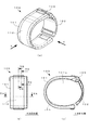
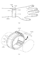
図1は、本発明に係る電子機器の一実施形態を示す概略構造図である。ここで、図1(a)は、本実施形態に係る電子機器の外観構成を示す概略斜視図であり、図1(b)は、図1(a)に示した電子機器を図面左斜め前方向(矢印X方向)から見た正面図であり、図1(c)は、図1(a)に示した電子機器を図面右斜め前方向(矢印Y方向)から見た側面図である。また、図2は、本実施形態に係る電子機器の、人体への装着例を示す概略図である。図3は、本実施形態に係る電子機器における機能構成を示す概略ブロック図である。 FIG. 1 is a schematic structural diagram showing an embodiment of an electronic apparatus according to the present invention. Here, FIG. 1A is a schematic perspective view showing an external configuration of the electronic device according to the present embodiment, and FIG. 1B is a front view of the electronic device shown in FIG. FIG. 1C is a side view of the electronic device shown in FIG. 1A viewed from the diagonally forward right direction (arrow Y direction) of the drawing. FIG. 2 is a schematic diagram showing an example of mounting the electronic device according to this embodiment on a human body. FIG. 3 is a schematic block diagram illustrating a functional configuration of the electronic apparatus according to the present embodiment.
(外観構成)
本発明の一実施形態に係る電子機器100は、例えば図1(a)〜(c)に示すように、大別して、湾曲形状を有する機器本体101と、機器本体101に対して回動可能に設けられた開閉部102と、を備えた外観形状を有している。
(Appearance configuration)
An
具体的には、機器本体101は、図1(a)〜(c)に示すように、略帯状の部材が長手方向に所定の曲率を有して湾曲し、側面側(図1(c)の矢印Y方向)から見て、略U字形状又は略C字形状に形成された構造を有している。機器本体101の長手方向の一方の端部(図1(a)、(c)の上方側の端部)には回転軸を備えた回動部103が設けられている。
Specifically, as shown in FIGS. 1A to 1C, the device
また、開閉部102は、図1(a)、(c)に示すように、略帯状の部材により形成され、一方の端部(図1(a)、(c)の上方側の端部)が回動部103を介して、機器本体101に接続されている。そして、開閉部102は、回動部103の回転軸を支点(中心)にして回動することにより、開閉部102の他方の端部(図1(a)、(c)の下方側の端部)が、機器本体101の他方の端部(図1(a)、(c)の下方側の端部)に対して、近接又は密着する閉止状態(図2(b)に実線で示す)と、所定の寸法以上離間する開放状態(図2(b)に二点鎖線で示す)に変化するように設計されている。
Further, as shown in FIGS. 1A and 1C, the opening /
(装着例)
このような構造を有する電子機器100において、図2(b)に二点鎖線で示すように、回動部103の回転軸を支点にして、開閉部102を機器本体101に対して回動させて、機器本体101と開閉部102の他方の端部同士が離間した開放状態にする。これにより、機器本体101の湾曲形状の内方の装着空間101sが開放され、電子機器100の手首UShへの装着、又は、手首UShからの離脱が可能な状態になる。そして、機器本体101と開閉部102の他方の端部同士が離間した開放状態において、機器本体101の装着空間101sに手首UShを挿入し、図2(b)に実線で示すように、開閉部102を機器本体101に対して回動させて、機器本体101と開閉部102の他方の端部同士が近接又は密着した閉止状態にする。ここで、開閉部102の回動動作は、予め設定された閉止状態となる位置でのみ回動が停止されるものであってもよいし、回動部103に設けられた回動調整部材によって所定の角度ごとに段階的に回動が一時停止できるものであってもよいし、無段階に回動が一時停止されるものであってもよい。これにより、機器本体101の装着空間101sが確定されて、図1(c)及び図2(a)、(b)に示すように、機器本体101及び開閉部102の内面側(装着空間101s側の面)が手首UShに接触又は密着して、電子機器100が手首UShに装着される。なお、図示を省略したが、電子機器100は、図2(b)に実線で示した閉止状態において、近接又は密着した機器本体101と開閉部102の他方の端部同士を、相互に接続するロック、アンロック機構を備えているものであってもよい。これにより、電子機器100を装着しロックすれば、電子機器100の使用中に、機器本体101と開閉部102の他方の端部同士が離間して手首UShから脱落する事故を確実に防止することができる。
(Installation example)
In the
(機能構成)
本実施形態に係る電子機器100は、例えば、次のような機能構成を有するものを適用することができる。電子機器100は、例えば図3に示すように、大別して、表示部110と、センサ部120と、操作部130と、通信部140と、制御部150と、記憶部160と、電源部170と、を有している。本実施形態においては、これらの構成が上述した機器本体101に内蔵されている。なお、機器本体101の内部構造(組み付け構造)については後述する。
(Functional configuration)
As the
表示部110は、例えば図1、図2に示すように、上述した湾曲形状を有する機器本体101の長手方向に沿って、外面側の略中央領域に帯状に延在するように設けられている。表示部110は、機器本体101の外面側に、例えば現在時刻やユーザの動作中や運動中に取得した生体情報や運動情報等を表示する。このような表示部110は、液晶方式や、有機EL等の発光素子方式、電子ペーパー方式等の各種の表示パネルを適用することができる。ここで、表示部110により表示される各種の情報は、カラー表示されるものであってもよいし、モノクロ表示されるものであってもよい。また、表示部110により表示される各種の情報は、文字情報や静止画像に限らず、動画像であってもよい。
For example, as shown in FIGS. 1 and 2, the
センサ部120は、例えば、ユーザの動作中や運動中の脈拍や体温、血圧等の生体情報、加速度や角速度等の運動情報、地理的な位置等の物理情報、気圧や湿度、地磁気等の環境情報を取得するセンサを有している。センサ部120により取得された生体情報や運動情報等は、記憶部160の所定の記憶領域にセンサデータとして保存される。
The
操作部130は、機器本体101や開閉部102の外面に設けられた操作ボタン(押しボタンやスライドボタン、タッチボタン等)や、上述した表示部110の視野側(前面側)に設けられたタッチパネル等のスイッチを有している。操作部130は、例えば電子機器100を起動するための電源操作や、電子機器100における各種の動作(表示部110の表示やセンサ部120の動作等)を設定するための操作に用いられる。
The
通信部140は、電子機器100の外部の機器(例えばスマートフォンやタブレット、パーソナルコンピュータ等)やネットワークとの間で、取得したセンサデータや各種信号の送受信を行うインターフェースとして機能する。ここで、通信部140を介して、電子機器100と外部の機器等との間で、センサデータ等を送受信する手法としては、各種の無線通信方式や有線通信方式が適用される。特に、無線通信方式を適用する場合には、通信部140は、例えばデジタル機器用の近距離無線通信規格であるブルートゥース(Bluetooth(登録商標))や、低消費電力型の通信規格として策定されたブルートゥースローエナジー(Bluetooth(登録商標) low energy(LE))、NFC(Near field communication)、ワイファイ(Wi-Fi;wireless fidelity(登録商標))等の通信方式を良好に適用することができる。
The
制御部150は、所定のプログラムを実行することにより、表示部110における表示動作や、センサ部120におけるセンシング動作、通信部140におけるセンサデータ等の送受信動作、記憶部160への書込み読出し動作、電源部170における電源供給動作等の、各種の動作を制御する。
The
記憶部160は、例えば、センサ部120により取得されたセンサデータ等を保存する。また、記憶部160は、制御部150により制御される、上記の各種の動作を実行する際に使用又は生成されるデータや情報を保存する。なお、記憶部160は、制御部150で実行されるプログラムを格納するものであってもよい。また、記憶部160は、例えばメモリカード等のリムーバブル記憶媒体としての形態を有し、電子機器100に対して着脱可能に設定されているものであってもよい。
The
電源部170は、上述した湾曲形状を有する機器本体101の長手方向に沿って帯状に延在する、薄型で湾曲した電池を有し、当該電池から出力される駆動電力を、電子機器100の各構成に供給する。ここで、本実施形態に適用される電池としては、例えばリチウムイオン電池やニッケル水素電池等の、繰り返し充放電が可能な二次電池が適用される。この場合、電源部170は、電池から各構成への駆動電力の供給動作に加え、電池への充電動作を行う。なお、電源部170は、上記の二次電池に加え、市販のボタン型電池等の一次電池や、振動や光、熱、電磁波等のエネルギーにより発電する環境発電(エナジーハーベスト)技術による電源等を併用する構造を有するものであってもよい。
The
(組み付け構造/断面構造)
次に、本実施形態に係る電子機器100の組み付け構造(内部構造)について説明する。
(Assembly structure / cross-sectional structure)
Next, an assembly structure (internal structure) of the
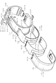
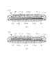
図4は、本実施形態に係る電子機器における組み付け構造(内部構造)を示す分解斜視図である。また、図5は、本実施形態に係る電子機器における要部断面図である。ここで、図5(a)は、図1(b)に示した電子機器におけるVA−VA線(本明細書においては図1中に示したローマ数字の「5」に対応する記号として便宜的に「V」を用いる。)に沿った断面構造を示す概略図である。また、図5(b)は、図1(b)に示した電子機器におけるVB−VB線に沿った断面構造を示す概略図であり、図5(c)は、図1(b)に示した電子機器におけるVC−VC線に沿った断面構造を示す概略図である。なお、図5においては、図示を明瞭にするために、断面を示すハッチングの一部を便宜的に省略して示した。 FIG. 4 is an exploded perspective view showing an assembly structure (internal structure) in the electronic apparatus according to the present embodiment. FIG. 5 is a cross-sectional view of the main part of the electronic apparatus according to the present embodiment. Here, FIG. 5A is a VA-VA line in the electronic device shown in FIG. 1B (in this specification, as a symbol corresponding to the Roman numeral “5” shown in FIG. 1 for convenience). Is a schematic diagram showing a cross-sectional structure along the line “V”. FIG. 5B is a schematic diagram illustrating a cross-sectional structure along the line VB-VB in the electronic device illustrated in FIG. 1B, and FIG. 5C is illustrated in FIG. It is the schematic which shows the cross-sectional structure along the VC-VC line in another electronic device. In FIG. 5, for the sake of clarity, a part of hatching showing a cross section is omitted for convenience.
図1に示した外観形状を有する機器本体101は、例えば図4、図5(a)に示すように、大別して、本体ケース11と、フレーム12と、電池13(図3に示した電源部170に対応する)と、回路基板14と、外装カバー15と、表示部16(図3に示した表示部110に対応する)と、を有している。そして、機器本体101は、本体ケース11と外装カバー15により形成される収納空間11sに、フレーム12や電池13、回路基板14、表示部16を収納した構造を有している。
1 is roughly divided into a
本体ケース11は、例えば図4に示すように、略帯状の絶縁性の部材により形成され、帯状の長手方向に所定の曲率で湾曲した湾曲形状を有している。また、本体ケース11は、少なくとも帯状の部材の長手方向に沿って、その両辺部が一方向(図4の外装カバー15方向)に屈曲又は突出した構造を有し、これにより図4、図5(a)に示すように、凹状の収納空間11sを備えた断面を有している。また、本体ケース11は、少なくとも帯状の部材の長手方向の一方の端部(図4の上方側の端部)に、開閉部102側に設けられた回動部103に接続するための取り付け穴H11が複数設けられている。なお、本体ケース11は、少なくとも本体ケース11に後述するフレーム12や外装カバー15が組み付けられた電子機器100を、ユーザが手首に装着して使用した際に、ある程度の変形を許容しつつ、収納空間11sの形状が保持できる程度の剛性や強度を備えるとともに、人体(肌)に接触しても違和感を持たない程度の質感を有していることが好ましい。
For example, as shown in FIG. 4, the
フレーム12は、例えば図4に示すように、帯状の平面形状を有する金属の薄板により形成され、本体ケース11が有する所定の曲率に対応した湾曲形状を有している。又は、フレーム12は、上記の所定の曲率に対応して湾曲する可撓性や変形性を有する程度の適度な剛性を有しており、外部からの一時的な小さい力によって機器本体101が撓みすぎたり、変形しすぎたりしないよう設定されている。また、フレーム12は、図4に示すように、帯状の薄板の長手方向の両端部を除く中間部分の幅方向の両辺部が幅方向に所定寸法だけ内側に位置するように欠落し且つ幅寸法が狭く形成された幅狭部12aが長手方向に沿って設けられている。また、フレーム12は、少なくとも帯状の薄板の長手方向の一方の端部(図4の上方側の端部)に、本体ケース11の収納空間11s内に組み付け固定するための取り付け穴H12が複数設けられている。また、少なくともフレーム12の長手方向の一方の端部には、後述する回路基板14との組み付け位置を確定するための基板固定ピンP12が設けられている。なお、フレーム12は、例えば鉄やステンレス、アルミニウム合金等の金属材料が適用されるが、適度の剛性を維持できれば金属材料に限らない。
For example, as shown in FIG. 4, the
電池13は、例えば図4に示すように、樹脂フィルムによるラミネートパッケージや薄型の金属パッケージ等を有する電池が帯状に形成され、上記のフレーム12の一面側(本体ケース11側)の面に一体的に固定されて、上記の所定の曲率に対応した湾曲形状を有している。又は、電池13は、上記の所定の曲率に対応して湾曲する可撓性や変形性を有している。ここで、電池13は、例えばフレーム12の略全域に対応した寸法の帯状の平面形状を有し、図4に示すように、フレーム12の一面側の略全域に取り付けられた構造を有している。これにより、フレーム12の幅狭部12aが形成された領域においては、幅狭部12aの両側に、電池13が露出した構造を有している。なお、図示を省略したが、このような電池13の出力端子は、例えばフレーム12の長手方向の両端部に対応する領域において、後述する回路基板14や表示部16に電気的に接続される。
For example, as shown in FIG. 4, the
回路基板14は、上述した機能構成において説明した通信部140や制御部150、記憶部160等が搭載される機能部品搭載部(第1の基板領域)と、信号配線やアンテナ配線等の配線パターンのみが形成されるパターン形成部(第2の基板領域)と、を有している。回路基板14は、例えば図4に示すように、上記のフレーム12及び電池13の略全域に対応した寸法の帯状の平面形状を有する絶縁性基板により形成され、帯状の長手方向の両端部には機能部品搭載部が設けられ、また、両端部を除く中間部分にはパターン形成部が設けられる。少なくともパターン形成部が設けられる回路基板14は、フレキシブルプリント基板(FPC)のような薄膜状又はフィルム状の薄型の絶縁性基板が帯状に形成され、例えば図4に示すように、上記の所定の曲率に対応した湾曲形状を有している。又は、パターン形成部が設けられる回路基板14は、上記の所定の曲率に対応して湾曲する可撓性や変形性を有している。また、パターン形成部が設けられる回路基板14は、図4に示すように、帯状の長手方向の両端部を除く中間部分に、略中央部が幅方向に所定寸法だけ欠落され且つ長手方向に延在する開口部14hが設けられている。すなわち、回路基板14は、開口部14hの幅方向両側にそれぞれ形成された2本の幅狭部14aにより長手方向の両端部が接続された構造を有している。ここで、回路基板14に設けられる開口部14hの幅寸法は、上記のフレーム12に設けられる幅狭部12aの幅寸法よりも大きくなるように設定されている。これにより、後述するように、本体ケース11に、フレーム12や電池13、回路基板14からなるユニットが略密着して組み付けられた状態で、図5(a)に示すように、回路基板14の開口部14hを形成する幅狭部14a、14a間に、フレーム12の幅狭部12aが位置するように形成されている。すなわち、フレーム12の幅狭部12aと回路基板14の幅狭部14aとは、フレーム12と回路基板14との積層方向(図4の左斜め前方向、又は、図5(a)の下方)から見て平面的に相互に重ならないように形成されているので、仮に機器本体101を撓ませたり、変形させたりしても回路基板14の幅狭部14aは、フレーム12の幅狭部12aと接触することがないように設定されている。また、電池13が経時的に膨張してフレーム12の幅狭部12aを回路基板14側に押しつけても、フレーム12の幅狭部12aは開口部14h内の収納空間11sにあるので、幅狭部14aがフレーム12の幅狭部12aと接触することがない。また、少なくとも回路基板14の長手方向の一方の端部(図4の上方側の端部)には、上記フレーム12との組み付け位置を確定するための位置決め穴H14が設けられている。なお、パターン形成部が設けられる回路基板14の幅狭部14aには、具体的には、例えばセンサ部120から出力される検出信号を制御部150に送信するためのセンサ信号線や、電源部170から供給される駆動電力を各構成に供給するための電源線、通信部140に適用される無線通信方式に対応したアンテナ配線等の配線パターンが形成される。ここで、開口部14hを形成する2本の幅狭部14aのうちの一方にセンサ信号線を形成し、他方に電源線を形成して、両者を開口部14hにより隔離することにより、電源線において発生する電界の影響を抑制して、センサ部120から出力される微弱な検出信号を制御部150に良好に送信することができる。また、回路基板14は、上記の機能部品や配線パターンが絶縁性基板の一面側にのみ搭載又は形成されているものであってもよいし、裏表両面側に搭載又は形成されているものであってもよい。ここで、回路基板14に搭載又は形成される機能部品や配線パターンは、周知の絶縁保護膜により被覆されて保護されている。
The
外装カバー15は、例えば図4に示すように、帯状の平面形状を有する絶縁性の薄板により形成され、上記の本体ケース11の湾曲形状に対応した湾曲形状を有している。又は、外装カバー15は、本体ケース11の湾曲形状に対応して湾曲する可撓性や変形性を有している。また、外装カバー15は、図5(a)に示すように、上記の本体ケース11に設けられた収納空間11sの開放端側(図面下方側)を閉止して密閉するように組み付けられる。ここで、外装カバー15は、少なくとも電子機器100の外部からの圧力(外圧)や周辺環境(温度や湿度、薬品等)に対して、収納空間11sに収納される各構成を保護することができる程度の特性(剛性や耐熱性、耐湿性、耐薬品性等)を有している。また、本実施形態においては、外装カバー15は、例えば透明な樹脂材料やガラス材料により形成され、外装カバー15の一面側(収納空間11s側)の面に、後述する表示部16が一体的に設けられた構造を有している。これにより、表示部16に表示された情報が、透明な外装カバー15を介して視野側に透過されて、ユーザに視認される。また、外装カバー15は、少なくとも帯状の薄板の長手方向の一方の端部(図4の上方側の端部)に、本体ケース11の収納空間11sを閉止するための取り付け穴H15が複数設けられている。
For example, as shown in FIG. 4, the
表示部16は、例えば図4に示すように、薄型の表示デバイスが帯状の平面形状を有するように形成され、上記の外装カバー15の一面側(収納空間11s側)の面に一体的に設けられ、外装カバー15の湾曲形状に対応した湾曲形状を有している。又は、表示部16は、外装カバー15の湾曲形状に対応して湾曲する可撓性や変形性を有している。表示部16は、可撓性のフィルム樹脂基板間に液晶が封入された液晶表示パネルや、可撓性のフィルム樹脂基板に有機EL層が設けられた有機EL表示パネルや、可撓性のフィルム樹脂基板間に色粒子が封入された電子ペーパー表示パネルのように、撓んだり、変形したりしても表示を維持することが可能である。ここで、表示部16に表示される各種の情報は、透明な外装カバー15を介してユーザの視野側に透過されて視認される。なお、図示を省略したが、例えば表示部16又は外装カバー15の長手方向の一方の端部には、表示部16のドライバICが設けられ、その近傍において回路基板14や電池13に電気的に接続される。
For example, as shown in FIG. 4, the
また、開閉部102は、例えば図4に示すように、略帯状の部材の長手方向の一方の端部(図4の上方側の端部)に、回動部103が設けられた構造を有している。回動部103は、回転軸を備え、回転軸を支点にして開閉部102が回動するように形成されている。また、回動部103は、少なくとも機器本体101と接続するための取り付け穴H13が複数設けられている。
Further, as shown in FIG. 4, for example, the opening /
(組み付け手順例)
次に、上述した電子機器の組み付け手順について、図4及び図5を用いて説明する。まず、図4及び図5(b)に示すように、回動部103に設けられた取り付け穴H13と、本体ケース11に設けられた取り付け穴H11と、フレーム12に設けられた取り付け穴H12との各位置を整合させて、本体ケース11及び回動部103の内方側(装着空間101s側;図5(b)の下方側)から雄ネジB11を挿通させて、ホルダーP11に設けられた雌ネジにネジ止めして固定する。これにより、本体ケース11の収納空間11sに、フレーム12、及び、フレーム12に一体的に設けられた電池13が、湾曲した状態で組み付けられる。
(Example of assembly procedure)
Next, a procedure for assembling the electronic device described above will be described with reference to FIGS. First, as shown in FIG. 4 and FIG. 5 (b), an
次いで、回路基板14に設けられた位置決め穴H14に、フレーム12に設けられた基板固定ピンP12を嵌合させて、フレーム12に対する回路基板14の組み付け位置を確定する。そして、フレーム12と回路基板14の長手方向の端部同士を、例えば接着剤や両面接着テープ等により接着して固定する。これにより、本体ケース11の収納空間11sに、各種の機能部品が搭載された回路基板14が、フレーム12に略密着して湾曲した状態で組み付けられる。また、このとき、フレーム12と回路基板14の長手方向の端部に対応する領域において、電池13と回路基板14が電気的に接続される。なお、フレーム12と回路基板14とを位置決めして固定する手法としては、上記の接着剤や両面接着テープの他に、ネジ固定や樹脂による溶着やホットメルト等を適用することができる。
Next, the board fixing pin P12 provided in the
次いで、図4及び図5(c)に示すように、本体ケース11の収納空間11sを閉止するように、表示部16が一体的に設けられた外装カバー15を配置し、外装カバー15に設けられた取り付け穴H15に外方側(図4及び図5(c)の上方側)から雄ネジB12を挿通させて、ホルダーP11に設けられた雌ネジにネジ止めして固定する。これにより、フレーム12と、電池13と、回路基板14とが組み付けられ、さらに表示部16が収納された本体ケース11の収納空間11sが密閉される。また、このとき、外装カバー15と回路基板14の長手方向の端部に対応する領域において、外装カバー15側に設けられた表示部16のドライバIC16aと、回路基板14のコネクタ16bや電池13とがフラットケーブルやバネ性の電極端子等を介して電気的に接続される。
Next, as shown in FIG. 4 and FIG. 5C, an
そして、外装カバー15を、ホルダーP11を介して本体ケース11にネジ止め固定した雄ネジB12及び取り付け穴H15の周辺を覆うようにカバー部品C11を取り付ける。これにより、密閉された本体ケース11の収納空間11sへの水分等の侵入を防止するとともに、電子機器100のデザイン性が高まる。なお、図4及び図5(b)、(c)においては、図示の都合上、回動部103が接続される機器本体101の一方の端部(図4の上方側の端部)について詳しく説明したが、他方の端部(図4の下方側の端部)についても同様にして組み付けを行って、フレーム12及び回路基板14、外装カバー15の両端部において本体ケース11に固定するものであってもよい。また、図4において、C12は、外装カバー15の他方の端部を、本体ケース11に固定する雄ネジ(図示を省略)周辺を覆うカバー部品であり、C13は、本体ケース11の他方の端部に取り付けられる、その他のカバー部品である。
Then, the cover part C11 is attached so as to cover the periphery of the male screw B12 and the attachment hole H15 in which the
次に、本実施形態に係る電子機器における作用効果について説明する。
図6は、本実施形態に係る電子機器における作用効果を説明するための概略断面図である。ここでは、図5(a)に示した断面図に基づいて作用効果を説明する。
Next, functions and effects of the electronic apparatus according to the present embodiment will be described.
FIG. 6 is a schematic cross-sectional view for explaining the function and effect of the electronic apparatus according to the present embodiment. Here, the function and effect will be described based on the cross-sectional view shown in FIG.
上述した背景技術において説明したように、手首や腕等に装着するリストバンド型の電子機器においては、薄型で、かつ、所定の曲率の湾曲形状を有している必要がある。このような電子機器を実現するためには、機器に内蔵される回路基板として、可撓性を有するFPCを適用する構造が考えられるが、この場合、回路基板自体の剛性や強度が低いため、電子機器の製造時や使用時に加わる外圧により撓みや変形が生じやすくなり、内蔵される各種の機能部品や構造部材が回路基板に接触して破損や剥離等を招く可能性がある。 As described in the background art described above, a wristband type electronic device worn on a wrist, an arm, or the like needs to be thin and have a curved shape with a predetermined curvature. In order to realize such an electronic device, a structure in which flexible FPC is applied as a circuit board incorporated in the device can be considered, but in this case, since the rigidity and strength of the circuit board itself are low, Bending and deformation are likely to occur due to external pressure applied during the manufacture and use of electronic equipment, and various built-in functional parts and structural members may come into contact with the circuit board and cause damage or peeling.
本実施形態に係る電子機器100においては、ある程度の剛性や強度を有する薄板により形成され、所定の曲率に対応した湾曲形状を有するフレーム12を備え、当該フレーム12に電池13や回路基板14が一体的又は部分的に固定された構造を有している。具体的には、図4及び図5に示したように、電子機器100は、フレーム12の一面側に二次電池からなる電池13が一体的に固定され、他面側(外装カバー15側)に通信部140や制御部150、記憶部160等の機能部品が搭載された回路基板14が両端固定された構造を有している。すなわち、電池13及び回路基板14は、フレーム12によりそれぞれの配置領域が確定(位置決め)されているとともに、図5(a)に示すように、フレーム12をはさむように両面側に密着して配置されている。これにより、本実施形態によれば、電子機器の製造時や使用時に加わる外圧に対して撓みや変形を抑制して、内蔵される機能部品や構造部材の破損や剥離等を抑制することができる。
The
これに加えて、本実施形態に係る電子機器においては、図4に示したように、フレーム12の両端部を除く中間部分に、長手方向に延在する幅狭部12aが設けられ、また、フレーム12に両端固定された回路基板14の両端部を除く中間部分に、長手方向に延在する開口部14h、及び、長手方向の両辺部に沿って(又は、開口部14hの両側に)延在する2本の幅狭部14aが設けられた構造を有している。ここで、開口部14hは、フレーム12に設けられた幅狭部12aに対応する領域に設けられるとともに、当該幅狭部12aよりも幅寸法が大きくなるように設定されている。
In addition to this, in the electronic device according to the present embodiment, as shown in FIG. 4, a narrow portion 12 a extending in the longitudinal direction is provided in an intermediate portion excluding both ends of the
そして、本実施形態において、フレーム12に電池13や回路基板14を積層するように一体的又は部分的に固定したユニットを、本体ケース11に組み付けた場合、フレーム12及び回路基板14の中間部分では、図5(a)に示したように、回路基板14の開口部14hを形成する幅狭部14a間に、フレーム12の幅狭部12aが位置して、両者が離間した状態となる。また、このフレーム12及び回路基板14の中間部分においては、機器本体101を厚み方向(図5(a)の上下方向)に見ると、フレーム12の一面側に設けられる電池13と、フレーム12の他面側に設けられる回路基板14の幅狭部14aとの間に、隙間11cが形成される。この隙間11cは、フレーム12に対して回路基板14を両端部で位置決め固定することにより、両者間に形成されるものである。そして、この隙間11cは、少なくとも電子機器を構成する部品や部材の製造ばらつきや組立て時の作業ばらつき、電子機器の使用時に生じる撓みや変形により、フレーム12及び回路基板14の曲率の違いに応じて周長が微妙に変化して生じる寸法差に対して、両者が接触しない程度の隙間に設定されている。
In this embodiment, when a unit that is integrally or partially fixed so that the
このように、本実施形態においては、フレーム12に電池13や回路基板14を積層するように固定し、かつ、フレーム12及び回路基板14の両端部を除く中間部分に形成された幅狭部12a及び14aが、フレーム12と回路基板14との積層方向から見て、平面的に重ならないように相互に離間して配置される。さらに、回路基板14の幅狭部14aが電池13に接触しないように所定の隙間11cを有するように形成される。これにより、本実施形態に係る構成を、薄型で所定の曲率の湾曲形状を有する電子機器に適用した場合、次のような作用効果を有している。
As described above, in the present embodiment, the
すなわち、図6(a)、(b)に示すように、フレーム12や回路基板14、電池13等を機器本体101に組み付ける際の、部品や部材の製造ばらつきや作業ばらつき、また、電子機器100の使用時に加わる外圧に起因して生じる寸法差に対して、回路基板14の開口部14h内に、フレーム12の幅狭部12aが入り込んで、幅狭部12a、14a同士が接触することがない。また、このとき、回路基板14と電池13との間に形成された隙間11cがなくならない程度に確保される。これにより、本実施形態によれば、上記のばらつきや寸法差を吸収することができ、電子機器の製造時や使用時における部品や部材の破損や剥離等の発生を防止して、良好な製品品質を実現することができる。
That is, as shown in FIGS. 6A and 6B, manufacturing variations and work variations of components and members when the
また、本実施形態においては、電子機器の各構成に駆動電流を供給するための電池13として、リチウムイオン電池等の二次電池を適用した構成を示した。このような電池においては、充電時や、使用による経年劣化により電池の筐体に膨れが生じることが知られている。本実施形態においては、上述したように、フレーム12及び回路基板14の両端部を除く中間部分において、幅狭部12a、14a同士が接触しないように離間して配置されているとともに、電池13と回路基板14の幅狭部14aとの間に隙間11cが形成されている。したがって、電池13で発生する膨れを隙間11cにより吸収することができ、機器本体101に内蔵される部品や部材相互の接触や干渉を防止して、良好な製品品質を実現することができる。
Moreover, in this embodiment, the structure which applied secondary batteries, such as a lithium ion battery, as the
(変形例)
次に、上述した実施形態に係る電子機器の変形例について説明する。
上述した実施形態においては、電子機器100を構成する機器本体101の本体ケース11に組み付けるフレーム12として、本体ケース11の曲率に対応して湾曲する金属の薄板が適用されることを説明した。ここで、本発明は、フレームを次の変形例のように構成することにより、新たな作用効果をさらに得ることができる。
(Modification)
Next, a modified example of the electronic device according to the above-described embodiment will be described.
In the above-described embodiment, it has been described that a metal thin plate that is curved corresponding to the curvature of the
すなわち、近年の携帯機器や情報機器においては、高機能化や高性能化により、制御部の演算処理スピードも高速化している。そのため、機器内部で発生する熱量も増大する傾向にある。また、近年のほとんどの携帯機器は、通信機能を備えており、外部の機器とのデータの送受信や連携動作は必要不可欠な機能になっている。このような状況に鑑み、本実施形態は以下のような変形例を有している。 That is, in recent portable devices and information devices, the calculation processing speed of the control unit has been increased due to higher functionality and higher performance. For this reason, the amount of heat generated inside the device also tends to increase. Also, most portable devices in recent years have a communication function, and data transmission / reception and cooperative operation with external devices are indispensable functions. In view of such a situation, this embodiment has the following modifications.
本実施形態に係る電子機器の第1の変形例は、上述した回路基板14に搭載される機能部品等のうち、動作に伴う発熱が生じる箇所又は機能部品搭載部、あるいは、その近傍の領域の回路基板14の裏面側(フレーム12側)において、フレーム12に接続固定した構造を有している。ここで、回路基板14とフレーム12との接続固定の手法としては、熱伝導性が高い材料を用いて接続することが好ましく、例えば熱伝導性の高い接着剤や、熱伝導性シートを挟んだ構造を適用することができる。これにより、回路基板14で発生する熱をフレーム12に良好に伝達して拡散させることができ、電子機器100の内部温度の上昇を抑えることができる。
The first modified example of the electronic device according to the present embodiment is a functional component or the like mounted on the
本実施形態に係る電子機器の第2の変形例は、上述した第1の変形例において、本体ケース11に組み付け固定されるフレーム12を、例えば長手方向に2分割(又は複数に分割)して熱源側と冷却側に分け、それぞれをヒートパイプにより接続した構造を有している。これにより、2分割したフレーム12間の熱の伝達、拡散を促進することができ、電子機器100の内部温度の上昇を抑えることができる。
The second modification of the electronic device according to the present embodiment is obtained by dividing the
本実施形態に係る電子機器の第3の変形例は、上述したフレーム12として、アルミニウム合金や銅合金等の熱伝導性の高い材料を適用し、さらに、当該フレーム12の一部を、機器本体101を構成する本体ケース11や外装カバー15から露出させて、外気に触れるように延在させた構造を有している。ここで、フレーム12の露出箇所は、一箇所であってもよいし、複数箇所であってもよい。このとき、露出したフレーム12が人体(ユーザの身体)に直接触れないように露出箇所が配置されていることが好ましい。これにより、フレーム12を放熱板として利用して、機器内部で発生した熱を電子機器100の外部に良好に放出することができ、内部温度の上昇を抑えることができる。
In the third modified example of the electronic apparatus according to the present embodiment, a material having high thermal conductivity such as an aluminum alloy or a copper alloy is applied as the
本実施形態に係る電子機器の第4の変形例は、上述したフレーム12に設けられた幅狭部12aに、通信部140に適用される無線通信方式に対応したアンテナ配線を配置した構造を有している。ここで、フレーム12に設けられた幅狭部12aにおいては、その周辺に回路部品等が搭載されておらず、ノイズの発生も少ないので、電波環境が比較的良好な状態にある。これにより、電子機器の外部の機器との間で良好な通信を実現することができる。
The fourth modified example of the electronic device according to the present embodiment has a structure in which antenna wiring corresponding to a wireless communication method applied to the
本実施形態に係る電子機器の第5の変形例は、上述したフレーム12として、ある程度の柔軟性を有する材料を適用した構造を有している。これにより、電子機器100を装着した際の人体への密着性を確保することができるとともに、外力による電子機器100の撓みや変形を抑制して、内蔵される部品や部材の破損や剥離等を抑制することができる。
A fifth modification of the electronic apparatus according to the present embodiment has a structure in which a material having a certain degree of flexibility is applied as the
本実施形態に係る電子機器の第6の変形例は、上述したフレーム12として、常温での形状保持性を有する形状記憶合金を適用した構造を有している。これにより、電子機器100を装着して常温で使用する際に、外力による電子機器100の撓みや変形に対して対抗力(耐性)を持たせることができる。
The sixth modification of the electronic device according to the present embodiment has a structure in which a shape memory alloy having shape retention at room temperature is applied as the
本実施形態に係る電子機器の第7の変形例は、上述したフレーム12として、熱による形状復元性を有する形状記憶合金を適用した構造を有している。これにより、外力による電子機器100の撓みや変形が生じた場合であっても、電子機器100を装着した際の体温等により形状を復元させることができる。
The seventh modified example of the electronic apparatus according to the present embodiment has a structure in which a shape memory alloy having a shape restoring property by heat is applied as the
なお、上述した実施形態においては、鉄やステンレス、アルミニウム合金等の金属材料からなるフレーム12を適用した構造を示したが、本発明はこれに限定されるものではない。本発明は、ある程度の剛性や強度を有する非金属の材料や構造を適用するものであってもよいし、熱伝導性の高い部材を適用するものであってもよい。
In the above-described embodiment, the structure in which the
また、上述した実施形態においては、フレーム12の両端部を除く中間部分に1本の幅狭部12aを設け、回路基板14の両端部を除く中間部分に2本の幅狭部14aからなる開口部14hを設けた構造を示したが、本発明はこれに限定されるものではない。すなわち、本発明は、上述した作用効果において説明したように、部品や部材の製造ばらつきや作業ばらつき、電子機器100の使用時に加わる外圧に起因する寸法差を、フレーム12や回路基板14の形状やその配置、隙間により吸収することができるものであれば、他の構造を有するものであってもよい。例えば、本発明は、フレームの両端部を除く中間部分に2本の幅狭部からなる開口部を設け、回路基板の両端部を除く中間部分に1本の幅狭部を設けた構造を有するものであってもよいし、フレーム及び回路基板のそれぞれの両端部を除く中間部分に、それぞれ1本の幅狭部を設けた構造を有するものであってもよい。
In the above-described embodiment, one narrow portion 12a is provided in an intermediate portion excluding both ends of the
また、上述した実施形態においては、電子機器100に表示部110を備え、各種の情報を表示する場合について説明したが、本発明はこれに限定されるものではない。すなわち、本発明は、表示部110を備えず、センサ部120により取得したセンサデータを記憶部160に蓄積する機能のみを有する電子機器であってもよい。この場合、外装カバー15は、外圧や周辺環境に対して、機器本体101に内蔵された回路基板14や電池13等を保護する機能のみを有することになる。
In the above-described embodiment, the case where the
また、上述した実施形態においては、電子機器100を人体の手首に装着する場合について説明したが、本発明はこれに限定されるものではない。すなわち、本発明は、手首や腕に装着する場合のほか、足首等の所定の曲率を有する部位に良好に装着して使用することができる。また、本発明は、装着対象を人体に限るものではなく、例えばペットの生体情報や物理情報等を取得するための首輪型の機器等に適用するものであってもよい。
In the above-described embodiment, the case where the
以上、本発明のいくつかの実施形態について説明したが、本発明は、上述した実施形態に限定されるものではなく、特許請求の範囲に記載された発明とその均等の範囲を含むものである。
以下に、本願出願の当初の特許請求の範囲に記載された発明を付記する。
As mentioned above, although some embodiment of this invention was described, this invention is not limited to embodiment mentioned above, It includes the invention described in the claim, and its equivalent range.
Hereinafter, the invention described in the scope of claims of the present application will be appended.
(付記)
[1]
少なくとも湾曲形状を有する本体ケースと、
前記本体ケースに設けられた収納空間に、前記湾曲形状に対応して組み付けられ、第1の幅狭部を有するフレームと、
前記収納空間に、前記フレームに密着して組み付けられ、第2の幅狭部を有する回路基板と、
を備え、
前記フレーム及び前記回路基板の積層方向から見て、前記第1の幅狭部及び前記第2の幅狭部が平面的に重ならないように配置されていることを特徴とする電子機器。
(Appendix)
[1]
A body case having at least a curved shape;
A frame having a first narrow portion assembled to the storage space provided in the main body case corresponding to the curved shape;
A circuit board that is assembled in close contact with the frame in the storage space and has a second narrow portion;
With
An electronic apparatus, wherein the first narrow portion and the second narrow portion are arranged so as not to overlap in plan view when viewed from the stacking direction of the frame and the circuit board.
[2]
前記第1の幅狭部及び前記第2の幅狭部は、それぞれ、前記フレーム及び前記回路基板の長手方向の両端部を除く中間部分に設けられていることを特徴とする[1]に記載の電子機器。
[2]
[1] The first narrow width portion and the second narrow width portion are provided in an intermediate portion excluding both ends of the frame and the circuit board in the longitudinal direction, respectively. Electronic equipment.
[3]
前記回路基板は、少なくとも、機能部品が搭載される第1の基板領域と、所定の配線パターンのみが設けられる第2の基板領域と、を有し、
前記第2の幅狭部に前記第2の基板領域が設定されていることを特徴とする[1]又は[2]に記載の電子機器。
[3]
The circuit board includes at least a first board area on which a functional component is mounted and a second board area on which only a predetermined wiring pattern is provided,
The electronic device according to [1] or [2], wherein the second substrate region is set in the second narrow portion.
[4]
前記第2の基板領域は、所定の信号が伝送される信号線、前記機能部品を駆動させるための電力を供給するための電源線、又は、前記機能部品において所定の電波を送受信するためのアンテナ線のいずれか一つ以上が設けられていることを特徴とする[3]に記載の電子機器。
[4]
The second substrate area includes a signal line for transmitting a predetermined signal, a power supply line for supplying power for driving the functional component, or an antenna for transmitting and receiving a predetermined radio wave in the functional component. One or more of the lines are provided, The electronic device as described in [3] characterized by the above-mentioned.
[5]
前記フレームは、少なくとも前記本体ケースに外圧が加わった場合であっても、前記湾曲形状に復元させる材料特性を有していることを特徴とする[1]乃至[4]のいずれかに記載の電子機器。
[5]
The frame according to any one of [1] to [4], wherein the frame has a material characteristic that restores the curved shape even when at least external pressure is applied to the main body case. Electronics.
[6]
前記フレームの一面側に配置された電池を備え、
前記回路基板は、前記フレームの他面側に配置されていることを特徴とする[1]乃至[5]のいずれかに記載の電子機器。
[6]
A battery disposed on one side of the frame;
The electronic device according to any one of [1] to [5], wherein the circuit board is disposed on the other surface side of the frame.
[7]
少なくとも前記回路基板と前記電池との間に所定の隙間を有していることを特徴とする[6]に記載の電子機器。
[7]
The electronic apparatus according to [6], wherein at least a predetermined gap is provided between the circuit board and the battery.
11 本体ケース
11s 収納空間
11c 隙間
12 フレーム
12a 幅狭部
13 電池
14 回路基板
14a 幅狭部
14h 開口部
15 外装カバー
16 表示部
100 電子機器
101 機器本体
101s 装着空間
102 開閉部
103 回動部
110 表示部
120 センサ部
130 操作部
140 通信部
150 制御部
160 記憶部
170 電源部
USh 手首
DESCRIPTION OF
Claims (13)
第1のフレーム部と、前記第1のフレーム部の幅より短い幅の第2のフレーム部と、を有し、前記収納部内に収納されるフレームと、
前記収納部内に前記フレームと積層するように収納され、前記フレームの積層方向から見て前記第2のフレーム部と重ならないように設けられている回路基板と、を備える、
ことを特徴とする電子機器。 A body case having a storage part at least partially curved;
A frame having a first frame portion and a second frame portion having a width shorter than a width of the first frame portion, and being housed in the housing portion ;
A circuit board that is housed in the housing part so as to be laminated with the frame, and is provided so as not to overlap the second frame part when viewed from the laminating direction of the frame .
An electronic device characterized by that.
前記第2のフレーム部の幅より広い幅の開口部と、
前記開口部の幅方向の少なくとも片側に位置する1本の幅狭回路基板部と、
を備える、
ことを特徴とする請求項1に記載の電子機器。 The circuit board is
An opening having a width wider than the width of the second frame portion;
One narrow circuit board portion located on at least one side in the width direction of the opening;
Comprising
The electronic device according to claim 1.
前記第2のフレーム部の幅より広い幅の開口部と、
前記開口部の幅方向の両方向に位置する2本の幅狭回路基板部と、を備える、
ことを特徴とする請求項1に記載の電子機器。 The circuit board is
An opening having a width wider than the width of the second frame portion;
Two narrow circuit board portions located in both directions in the width direction of the opening,
The electronic device according to claim 1 .
ことを特徴とする請求項3に記載の電子機器。 A sensor signal line is formed on one narrow circuit board part of the two narrow circuit board parts, and a power supply line is isolated from the sensor signal line on the other narrow circuit board part by the opening. Formed,
The electronic device according to claim 3.
ことを特徴とする請求項2乃至4のいずれか一項に記載の電子機器。 The second frame is provided in an intermediate portion excluding both end portions in the longitudinal direction of the frame, and the narrow circuit board portion is provided in an intermediate portion excluding both end portions in the longitudinal direction of the circuit board. Yes,
The electronic device according to claim 2 , wherein the electronic device is an electronic device.
ことを特徴とする請求項2乃至5のいずれか一項に記載の電子機器。 The frame and the circuit board are stacked and stored in the storage portion so that the second frame portion is positioned in the opening.
The electronic device according to claim 2 , wherein the electronic device is an electronic device.
ことを特徴とする請求項2乃至6のいずれか一項に記載の電子機器。 The circuit board and the second frame portion have flexibility and deformability, and are provided so as not to overlap when viewed from the frame stacking direction even when the curved shape is deformed. Yes,
The electronic device according to claim 2 , wherein the electronic device is an electronic device.
前記幅狭回路基板部に前記第2の基板領域が設定されている、 The second substrate region is set in the narrow circuit board part;
ことを特徴とする請求項2乃至7のいずれか一項に記載の電子機器。The electronic device according to claim 2, wherein the electronic device is an electronic device.
ことを特徴とする請求項8に記載の電子機器。9. The electronic apparatus according to claim 8, wherein
ことを特徴とする請求項1乃至9のいずれか一項に記載の電子機器。The electronic device according to claim 1, wherein the electronic device is an electronic device.
前記回路基板は、前記フレームの他面側に配置されている、The circuit board is disposed on the other surface side of the frame.
ことを特徴とする請求項1乃至10のいずれか一項に記載の電子機器。The electronic device according to claim 1, wherein the electronic device is an electronic device.
ことを特徴とする請求項11に記載の電子機器。The electronic device according to claim 11, wherein
ことを特徴とする請求項1乃至12のいずれか一項に記載の電子機器。 The frame has a narrow portion formed such that both sides in the width direction of the intermediate portion excluding both ends in the longitudinal direction of the belt-like thin plate are missing so as to be located inward by a predetermined dimension in the width direction and the width dimension is narrowed. Provided along the longitudinal direction,
The electronic device according to claim 1, wherein the electronic device is an electronic device .
Priority Applications (3)
| Application Number | Priority Date | Filing Date | Title |
|---|---|---|---|
| JP2014251388A JP6187776B2 (en) | 2014-12-12 | 2014-12-12 | Electronics |
| US14/885,302 US9693731B2 (en) | 2014-12-12 | 2015-10-16 | Electronic device |
| CN201510883076.8A CN105700339B (en) | 2014-12-12 | 2015-12-04 | Electronic equipment |
Applications Claiming Priority (1)
| Application Number | Priority Date | Filing Date | Title |
|---|---|---|---|
| JP2014251388A JP6187776B2 (en) | 2014-12-12 | 2014-12-12 | Electronics |
Publications (3)
| Publication Number | Publication Date |
|---|---|
| JP2016114393A JP2016114393A (en) | 2016-06-23 |
| JP2016114393A5 JP2016114393A5 (en) | 2016-08-12 |
| JP6187776B2 true JP6187776B2 (en) | 2017-08-30 |
Family
ID=56112564
Family Applications (1)
| Application Number | Title | Priority Date | Filing Date |
|---|---|---|---|
| JP2014251388A Active JP6187776B2 (en) | 2014-12-12 | 2014-12-12 | Electronics |
Country Status (3)
| Country | Link |
|---|---|
| US (1) | US9693731B2 (en) |
| JP (1) | JP6187776B2 (en) |
| CN (1) | CN105700339B (en) |
Families Citing this family (6)
| Publication number | Priority date | Publication date | Assignee | Title |
|---|---|---|---|---|
| CN106125542B (en) * | 2016-06-20 | 2018-05-01 | 武汉华星光电技术有限公司 | Intelligent watch and its multiple digital operation method |
| US11389640B2 (en) * | 2017-01-19 | 2022-07-19 | HighDim GmbH | Devices and methods for determining heart function of a living subject |
| JP6978920B2 (en) * | 2017-12-13 | 2021-12-08 | Fdk株式会社 | Battery module |
| CN108665811A (en) * | 2018-06-27 | 2018-10-16 | 云谷(固安)科技有限公司 | Cover board, flexible display screen and flexible electronic devices |
| JP7237576B2 (en) * | 2018-12-27 | 2023-03-13 | オムロンヘルスケア株式会社 | Blood pressure measuring device |
| CN111712037A (en) * | 2020-06-29 | 2020-09-25 | 京东方科技集团股份有限公司 | Integrated structure of circuit board, display module and electronic equipment |
Family Cites Families (25)
| Publication number | Priority date | Publication date | Assignee | Title |
|---|---|---|---|---|
| JP2000209319A (en) | 1999-01-18 | 2000-07-28 | Hiroshi Fujii | Shape of portable telephone set |
| GB0302690D0 (en) * | 2003-02-06 | 2003-03-12 | Snapwatch Ltd | Display apparatus |
| JP4543772B2 (en) * | 2003-09-19 | 2010-09-15 | セイコーエプソン株式会社 | Electro-optical device and electronic apparatus |
| JP2005250442A (en) | 2004-01-30 | 2005-09-15 | Seiko Epson Corp | Display device, method of controlling display device, control program, and recording medium |
| CN200990745Y (en) * | 2005-03-04 | 2007-12-12 | 精工爱普生株式会社 | Personal electronic instrument and portable instrument |
| JP2007078670A (en) | 2005-03-04 | 2007-03-29 | Seiko Epson Corp | Wearable electronic device, method for manufacturing portable device, and the portable device |
| JP4153512B2 (en) | 2005-09-12 | 2008-09-24 | 株式会社ダスキンヘルスケア | Aerobic exercise maintenance equipment |
| JP2008008832A (en) * | 2006-06-30 | 2008-01-17 | Seiko Epson Corp | Timepiece |
| US7722245B2 (en) * | 2006-10-06 | 2010-05-25 | Seiko Epson Corporation | Display device |
| JP5135811B2 (en) * | 2007-02-01 | 2013-02-06 | セイコーエプソン株式会社 | Display device |
| JP2008139163A (en) * | 2006-12-01 | 2008-06-19 | Seiko Epson Corp | Indication device and indication method |
| US7518959B2 (en) * | 2006-12-01 | 2009-04-14 | Seiko Epson Corporation | Display device and display method |
| FR2923979B1 (en) * | 2007-11-15 | 2009-12-04 | Sagem Monetel | DEVICE FOR PROTECTING THE PINS OF AN ELECTRONIC COMPONENT |
| KR101659023B1 (en) * | 2010-03-15 | 2016-09-23 | 엘지전자 주식회사 | Watch type mobile terminal |
| EP3013128A1 (en) * | 2010-07-26 | 2016-04-27 | Nippon Mektron Ltd. | Flexible printed circuit board and method of manufacturing the same |
| JP5136723B2 (en) * | 2010-12-03 | 2013-02-06 | 株式会社村田製作所 | Electronics |
| US9131039B2 (en) * | 2011-12-22 | 2015-09-08 | Nokia Technologies Oy | Piezoelectric actuator interface and method |
| US9190720B2 (en) * | 2012-03-23 | 2015-11-17 | Apple Inc. | Flexible printed circuit structures |
| US9060433B2 (en) * | 2013-01-04 | 2015-06-16 | International Business Machines Corporation | Thermal dissipative retractable flex assembly |
| TWI637669B (en) * | 2013-07-12 | 2018-10-01 | 易鼎股份有限公司 | Wearable assembly method of flexible circuit board and shaft member |
| US20150136448A1 (en) * | 2013-11-18 | 2015-05-21 | Kabushiki Kaisha Toshiba | Flexible Printed Wiring Board and Electronic Apparatus |
| KR20160103073A (en) * | 2013-12-24 | 2016-08-31 | 폴리에라 코퍼레이션 | Support structures for a flexible electronic component |
| US9158285B2 (en) * | 2014-01-06 | 2015-10-13 | Central Standard Timing, LLC | Flexible wristwatch with segmented e-paper display |
| US9357654B2 (en) * | 2014-03-03 | 2016-05-31 | Apple Inc. | Low-profile plug with cam and flexible circuit board |
| US20150373830A1 (en) * | 2014-06-19 | 2015-12-24 | Kabushiki Kaisha Toshiba | Composite substrate including foldable portion |
-
2014
- 2014-12-12 JP JP2014251388A patent/JP6187776B2/en active Active
-
2015
- 2015-10-16 US US14/885,302 patent/US9693731B2/en active Active
- 2015-12-04 CN CN201510883076.8A patent/CN105700339B/en active Active
Also Published As
| Publication number | Publication date |
|---|---|
| CN105700339B (en) | 2018-09-04 |
| JP2016114393A (en) | 2016-06-23 |
| US20160174399A1 (en) | 2016-06-16 |
| CN105700339A (en) | 2016-06-22 |
| US9693731B2 (en) | 2017-07-04 |
Similar Documents
| Publication | Publication Date | Title |
|---|---|---|
| JP6187776B2 (en) | Electronics | |
| CN110429373B (en) | Antenna assembly for a watchband | |
| CN111417894B (en) | Electronic device having display with extended edge | |
| CN104470299B (en) | Electronic equipment | |
| US9939787B2 (en) | Wearable electronic device with electronic component in strap | |
| US9720376B2 (en) | Band type electronic device and substrate arrangement method | |
| TWI718833B (en) | Electronic device | |
| EP3180460B1 (en) | Electronic device with plated electrical contact | |
| EP3148409B1 (en) | Wearable electronic device | |
| CN205681514U (en) | Mobile electronic equipment shell | |
| TW201605117A (en) | Antenna for electronic device | |
| KR20170015902A (en) | Battery compartments for wearable electronic device | |
| CN107533345A (en) | Wearable device | |
| US10264336B2 (en) | Electronic device and conductive structure | |
| US10114411B2 (en) | Electronic device and manufacturing method therefor | |
| US11123016B2 (en) | Portable bio information measuring device | |
| KR20190067872A (en) | Watch type terminal | |
| KR20100103308A (en) | Watch type mobile terminal | |
| KR20200001529A (en) | patch type thermometer and the method of manufacturing the same | |
| JP2016142888A (en) | Display unit, information display method, and information display program | |
| CN117651928A (en) | Electronic device including structure for preventing damage to flexible printed circuit board | |
| JP2007263719A (en) | Wrist watch type electronic device | |
| KR102402335B1 (en) | Adhesive band for fixing patch type thermometer and patch type thermometer including the same | |
| US20220094063A1 (en) | Wearable terminal | |
| TWI548970B (en) | Wearable electronic device and core module thereof |
Legal Events
| Date | Code | Title | Description |
|---|---|---|---|
| A521 | Written amendment |
Free format text: JAPANESE INTERMEDIATE CODE: A523 Effective date: 20160624 |
|
| A621 | Written request for application examination |
Free format text: JAPANESE INTERMEDIATE CODE: A621 Effective date: 20160624 |
|
| TRDD | Decision of grant or rejection written | ||
| A01 | Written decision to grant a patent or to grant a registration (utility model) |
Free format text: JAPANESE INTERMEDIATE CODE: A01 Effective date: 20170705 |
|
| A61 | First payment of annual fees (during grant procedure) |
Free format text: JAPANESE INTERMEDIATE CODE: A61 Effective date: 20170718 |
|
| R150 | Certificate of patent or registration of utility model |
Ref document number: 6187776 Country of ref document: JP Free format text: JAPANESE INTERMEDIATE CODE: R150 |