JP6167108B2 - Fixing apparatus and cleavage method for cleaving a bonded wafer structure - Google Patents
Fixing apparatus and cleavage method for cleaving a bonded wafer structure Download PDFInfo
- Publication number
- JP6167108B2 JP6167108B2 JP2014539062A JP2014539062A JP6167108B2 JP 6167108 B2 JP6167108 B2 JP 6167108B2 JP 2014539062 A JP2014539062 A JP 2014539062A JP 2014539062 A JP2014539062 A JP 2014539062A JP 6167108 B2 JP6167108 B2 JP 6167108B2
- Authority
- JP
- Japan
- Prior art keywords
- wafer
- clamp
- end surface
- gripping member
- arm
- Prior art date
- Legal status (The legal status is an assumption and is not a legal conclusion. Google has not performed a legal analysis and makes no representation as to the accuracy of the status listed.)
- Active
Links
Images


Classifications
-
- B—PERFORMING OPERATIONS; TRANSPORTING
- B32—LAYERED PRODUCTS
- B32B—LAYERED PRODUCTS, i.e. PRODUCTS BUILT-UP OF STRATA OF FLAT OR NON-FLAT, e.g. CELLULAR OR HONEYCOMB, FORM
- B32B43/00—Operations specially adapted for layered products and not otherwise provided for, e.g. repairing; Apparatus therefor
- B32B43/006—Delaminating
-
- B—PERFORMING OPERATIONS; TRANSPORTING
- B32—LAYERED PRODUCTS
- B32B—LAYERED PRODUCTS, i.e. PRODUCTS BUILT-UP OF STRATA OF FLAT OR NON-FLAT, e.g. CELLULAR OR HONEYCOMB, FORM
- B32B38/00—Ancillary operations in connection with laminating processes
- B32B38/10—Removing layers, or parts of layers, mechanically or chemically
-
- H—ELECTRICITY
- H01—ELECTRIC ELEMENTS
- H01L—SEMICONDUCTOR DEVICES NOT COVERED BY CLASS H10
- H01L21/00—Processes or apparatus adapted for the manufacture or treatment of semiconductor or solid state devices or of parts thereof
- H01L21/67—Apparatus specially adapted for handling semiconductor or electric solid state devices during manufacture or treatment thereof; Apparatus specially adapted for handling wafers during manufacture or treatment of semiconductor or electric solid state devices or components ; Apparatus not specifically provided for elsewhere
- H01L21/67005—Apparatus not specifically provided for elsewhere
- H01L21/67011—Apparatus for manufacture or treatment
- H01L21/67092—Apparatus for mechanical treatment
-
- C—CHEMISTRY; METALLURGY
- C09—DYES; PAINTS; POLISHES; NATURAL RESINS; ADHESIVES; COMPOSITIONS NOT OTHERWISE PROVIDED FOR; APPLICATIONS OF MATERIALS NOT OTHERWISE PROVIDED FOR
- C09J—ADHESIVES; NON-MECHANICAL ASPECTS OF ADHESIVE PROCESSES IN GENERAL; ADHESIVE PROCESSES NOT PROVIDED FOR ELSEWHERE; USE OF MATERIALS AS ADHESIVES
- C09J2301/00—Additional features of adhesives in the form of films or foils
- C09J2301/50—Additional features of adhesives in the form of films or foils characterized by process specific features
- C09J2301/502—Additional features of adhesives in the form of films or foils characterized by process specific features process for debonding adherents
-
- H—ELECTRICITY
- H01—ELECTRIC ELEMENTS
- H01L—SEMICONDUCTOR DEVICES NOT COVERED BY CLASS H10
- H01L2221/00—Processes or apparatus adapted for the manufacture or treatment of semiconductor or solid state devices or of parts thereof covered by H01L21/00
- H01L2221/67—Apparatus for handling semiconductor or electric solid state devices during manufacture or treatment thereof; Apparatus for handling wafers during manufacture or treatment of semiconductor or electric solid state devices or components; Apparatus not specifically provided for elsewhere
- H01L2221/683—Apparatus for handling semiconductor or electric solid state devices during manufacture or treatment thereof; Apparatus for handling wafers during manufacture or treatment of semiconductor or electric solid state devices or components; Apparatus not specifically provided for elsewhere for supporting or gripping
- H01L2221/68304—Apparatus for handling semiconductor or electric solid state devices during manufacture or treatment thereof; Apparatus for handling wafers during manufacture or treatment of semiconductor or electric solid state devices or components; Apparatus not specifically provided for elsewhere for supporting or gripping using temporarily an auxiliary support
- H01L2221/68381—Details of chemical or physical process used for separating the auxiliary support from a device or wafer
- H01L2221/68386—Separation by peeling
- H01L2221/6839—Separation by peeling using peeling wedge or knife or bar
-
- Y—GENERAL TAGGING OF NEW TECHNOLOGICAL DEVELOPMENTS; GENERAL TAGGING OF CROSS-SECTIONAL TECHNOLOGIES SPANNING OVER SEVERAL SECTIONS OF THE IPC; TECHNICAL SUBJECTS COVERED BY FORMER USPC CROSS-REFERENCE ART COLLECTIONS [XRACs] AND DIGESTS
- Y10—TECHNICAL SUBJECTS COVERED BY FORMER USPC
- Y10S—TECHNICAL SUBJECTS COVERED BY FORMER USPC CROSS-REFERENCE ART COLLECTIONS [XRACs] AND DIGESTS
- Y10S156/00—Adhesive bonding and miscellaneous chemical manufacture
- Y10S156/918—Delaminating processes adapted for specified product, e.g. delaminating medical specimen slide
- Y10S156/93—Semiconductive product delaminating, e.g. delaminating emiconductive wafer from underlayer
-
- Y—GENERAL TAGGING OF NEW TECHNOLOGICAL DEVELOPMENTS; GENERAL TAGGING OF CROSS-SECTIONAL TECHNOLOGIES SPANNING OVER SEVERAL SECTIONS OF THE IPC; TECHNICAL SUBJECTS COVERED BY FORMER USPC CROSS-REFERENCE ART COLLECTIONS [XRACs] AND DIGESTS
- Y10—TECHNICAL SUBJECTS COVERED BY FORMER USPC
- Y10S—TECHNICAL SUBJECTS COVERED BY FORMER USPC CROSS-REFERENCE ART COLLECTIONS [XRACs] AND DIGESTS
- Y10S156/00—Adhesive bonding and miscellaneous chemical manufacture
- Y10S156/934—Apparatus having delaminating means adapted for delaminating a specified article
- Y10S156/941—Means for delaminating semiconductive product
-
- Y—GENERAL TAGGING OF NEW TECHNOLOGICAL DEVELOPMENTS; GENERAL TAGGING OF CROSS-SECTIONAL TECHNOLOGIES SPANNING OVER SEVERAL SECTIONS OF THE IPC; TECHNICAL SUBJECTS COVERED BY FORMER USPC CROSS-REFERENCE ART COLLECTIONS [XRACs] AND DIGESTS
- Y10—TECHNICAL SUBJECTS COVERED BY FORMER USPC
- Y10T—TECHNICAL SUBJECTS COVERED BY FORMER US CLASSIFICATION
- Y10T156/00—Adhesive bonding and miscellaneous chemical manufacture
- Y10T156/11—Methods of delaminating, per se; i.e., separating at bonding face
- Y10T156/1168—Gripping and pulling work apart during delaminating
- Y10T156/1179—Gripping and pulling work apart during delaminating with poking during delaminating [e.g., jabbing, etc.]
- Y10T156/1184—Piercing layer during delaminating [e.g., cutting, etc.]
-
- Y—GENERAL TAGGING OF NEW TECHNOLOGICAL DEVELOPMENTS; GENERAL TAGGING OF CROSS-SECTIONAL TECHNOLOGIES SPANNING OVER SEVERAL SECTIONS OF THE IPC; TECHNICAL SUBJECTS COVERED BY FORMER USPC CROSS-REFERENCE ART COLLECTIONS [XRACs] AND DIGESTS
- Y10—TECHNICAL SUBJECTS COVERED BY FORMER USPC
- Y10T—TECHNICAL SUBJECTS COVERED BY FORMER US CLASSIFICATION
- Y10T156/00—Adhesive bonding and miscellaneous chemical manufacture
- Y10T156/19—Delaminating means
- Y10T156/1961—Severing delaminating means [e.g., chisel, etc.]
-
- Y—GENERAL TAGGING OF NEW TECHNOLOGICAL DEVELOPMENTS; GENERAL TAGGING OF CROSS-SECTIONAL TECHNOLOGIES SPANNING OVER SEVERAL SECTIONS OF THE IPC; TECHNICAL SUBJECTS COVERED BY FORMER USPC CROSS-REFERENCE ART COLLECTIONS [XRACs] AND DIGESTS
- Y10—TECHNICAL SUBJECTS COVERED BY FORMER USPC
- Y10T—TECHNICAL SUBJECTS COVERED BY FORMER US CLASSIFICATION
- Y10T156/00—Adhesive bonding and miscellaneous chemical manufacture
- Y10T156/19—Delaminating means
- Y10T156/1978—Delaminating bending means
-
- Y—GENERAL TAGGING OF NEW TECHNOLOGICAL DEVELOPMENTS; GENERAL TAGGING OF CROSS-SECTIONAL TECHNOLOGIES SPANNING OVER SEVERAL SECTIONS OF THE IPC; TECHNICAL SUBJECTS COVERED BY FORMER USPC CROSS-REFERENCE ART COLLECTIONS [XRACs] AND DIGESTS
- Y10—TECHNICAL SUBJECTS COVERED BY FORMER USPC
- Y10T—TECHNICAL SUBJECTS COVERED BY FORMER US CLASSIFICATION
- Y10T225/00—Severing by tearing or breaking
- Y10T225/10—Methods
- Y10T225/12—With preliminary weakening
-
- Y—GENERAL TAGGING OF NEW TECHNOLOGICAL DEVELOPMENTS; GENERAL TAGGING OF CROSS-SECTIONAL TECHNOLOGIES SPANNING OVER SEVERAL SECTIONS OF THE IPC; TECHNICAL SUBJECTS COVERED BY FORMER USPC CROSS-REFERENCE ART COLLECTIONS [XRACs] AND DIGESTS
- Y10—TECHNICAL SUBJECTS COVERED BY FORMER USPC
- Y10T—TECHNICAL SUBJECTS COVERED BY FORMER US CLASSIFICATION
- Y10T225/00—Severing by tearing or breaking
- Y10T225/30—Breaking or tearing apparatus
- Y10T225/35—Work-parting pullers [bursters]
- Y10T225/357—Relatively movable clamps
-
- Y—GENERAL TAGGING OF NEW TECHNOLOGICAL DEVELOPMENTS; GENERAL TAGGING OF CROSS-SECTIONAL TECHNOLOGIES SPANNING OVER SEVERAL SECTIONS OF THE IPC; TECHNICAL SUBJECTS COVERED BY FORMER USPC CROSS-REFERENCE ART COLLECTIONS [XRACs] AND DIGESTS
- Y10—TECHNICAL SUBJECTS COVERED BY FORMER USPC
- Y10T—TECHNICAL SUBJECTS COVERED BY FORMER US CLASSIFICATION
- Y10T225/00—Severing by tearing or breaking
- Y10T225/30—Breaking or tearing apparatus
- Y10T225/393—Web restrainer
Description
関連出願の相互参照
本出願は、2011年10月31日に出願された米国仮出願第61/553,447号の利益を主張する。当該出願は、全体として引用により本明細書において援用される。
This application claims the benefit of US Provisional Application No. 61 / 553,447, filed Oct. 31, 2011. This application is incorporated herein by reference in its entirety.
本開示の技術分野
本開示は、概して、結合ウェハ構造体を劈開させるための装置及び方法に関し、より詳細には、当該結合ウェハ構造体を劈開させるように動作するクランプに関連する装置及び方法に関する。
TECHNICAL FIELD OF THE DISCLOSURE The present disclosure relates generally to an apparatus and method for cleaving a bonded wafer structure, and more particularly to an apparatus and method associated with a clamp that operates to cleave the bonded wafer structure. .
半導体ウェハは、概して、単結晶インゴット(例えば、シリコンインゴット)から作製される。当該単結晶インゴットは、スライスされて複数のウェハになる。当該複数のウェハは、複数の製品ウェハを製造するために、研削及び/又は研磨される。本明細書において、シリコンにより構成された半導体ウェハについて言及するが、砒化ゲルマニウム若しくは砒化ガリウム等の他の材料を同じように用いてもよい。 Semiconductor wafers are generally made from single crystal ingots (eg, silicon ingots). The single crystal ingot is sliced into a plurality of wafers. The plurality of wafers are ground and / or polished to produce a plurality of product wafers. In this specification, reference is made to a semiconductor wafer made of silicon, but other materials such as germanium arsenide or gallium arsenide may be used as well.
一のタイプのウェハとして、シリコン−オン−インシュレータ(SOI)ウェハがある。SOIウェハには、シリコン基板上に絶縁層(例えば、酸化物層)が配され、さらに絶縁層の上にシリコン薄層が形成されたものが含まれる。 One type of wafer is a silicon-on-insulator (SOI) wafer. SOI wafers include those in which an insulating layer (for example, an oxide layer) is disposed on a silicon substrate and a thin silicon layer is further formed on the insulating layer.
SOIウェハを作製する典型的なプロセスには、ドナーウェハ及び/又はハンドルウェハの研磨されたフロント表面上に酸化物層を析出させることが含まれる。粒子(例えば、水素原子、若しくは、水素原子とヘリウム原子との組み合わせ)を、ドナーウェハのフロント表面から下の所定の深さの位置に注入する。注入された粒子は、ドナーウェハ内の、粒子が注入された特定の深さの位置において、劈開面を形成する。注入プロセスの間にウェハ上に析出された有機化合物を除去するため、ドナーウェハの表面は洗浄される。 A typical process for making an SOI wafer involves depositing an oxide layer on the polished front surface of a donor wafer and / or handle wafer. Particles (eg, hydrogen atoms or a combination of hydrogen and helium atoms) are implanted at a predetermined depth below the front surface of the donor wafer. The implanted particles form a cleavage plane in the donor wafer at a specific depth where the particles are implanted. The surface of the donor wafer is cleaned to remove organic compounds deposited on the wafer during the implantation process.
ドナーウェハのフロント表面は、その後、親水性結合プロセスにより、ハンドルウェハと結合され、結合ウェハ対が形成される。ドナーウェハとハンドルウェハとは、それらのウェハの表面を、例えば、酸素含有若しくは窒素含有のプラズマに供することにより、一体に結合される。通常表面活性化と称されるあるプロセスにおいて、プラズマに供することにより、表面の構造が変更される。その後、ウェハが押し付けられ、それらの間に結合が形成される。この結合は比較的弱く、さらなる加工処理が行われる前に、この結合を強固にしなければならない。 The front surface of the donor wafer is then bonded to the handle wafer by a hydrophilic bonding process to form a bonded wafer pair. The donor wafer and the handle wafer are bonded together by subjecting the surfaces of the wafers to, for example, an oxygen-containing or nitrogen-containing plasma. In one process, commonly referred to as surface activation, the surface structure is altered by subjecting it to plasma. The wafer is then pressed and a bond is formed between them. This bond is relatively weak and must be strengthened before further processing can take place.
いくつかのプロセスにおいて、ドナーウェハとハンドルウェハとの間(すなわち、結合ウェハ中)の親水性結合は、およそ300℃〜500℃の温度で結合ウェハ対を加熱若しくはアニールすることにより強固なものとされる。昇温により、隣接するドナーウェハの表面とハンドルウェハの表面との間に共有結合を形成することができ、それにより、ドナーウェハとハンドルウェハとの間の結合が強固なものとされる。先にドナーウェハ中に粒子を注入し、併せて結合ウェハの加熱若しくはアニールすることにより、劈開面が脆弱化される。その後、ドナーウェハの一部が劈開面に沿って結合ウェハ対から分離(すなわち、劈開)され、SOIウェハが形成される。 In some processes, the hydrophilic bond between the donor wafer and the handle wafer (ie, in the bonded wafer) is strengthened by heating or annealing the bonded wafer pair at a temperature of approximately 300 ° C to 500 ° C. The The elevated temperature can form a covalent bond between the surface of the adjacent donor wafer and the surface of the handle wafer, thereby strengthening the bond between the donor wafer and the handle wafer. The cleavage plane is weakened by first injecting the particles into the donor wafer and heating or annealing the bonded wafer. Thereafter, a portion of the donor wafer is separated (ie, cleaved) from the bonded wafer pair along the cleavage plane to form an SOI wafer.
まず最初に、結合ウェハからドナーウェハの一部を引き離すために結合ウェハの両サイドに対して機械的力を垂直な方向に加える固定具(fixture)に結合ウェハが配置される。いくつかの方法によれば、吸引カップを用いて当該機械的力を加える。ドナーウェハの一部を分離することは、ドナーウェハとハンドルウェハとの間の界面において、結合ウェハのエッジに機械的ウェッジを押し付けることにより開始される。機械的力を加えることにより、劈開面に沿った劈開の進展が開始される。その後、吸引カップにより加えられた機械的力により、結合ウェハからドナーウェハの一部が引き離され、それにより、SOIウェハが形成される。 First, the bonded wafer is placed in a fixture that applies a mechanical force in a direction perpendicular to both sides of the bonded wafer to separate a portion of the donor wafer from the bonded wafer. According to some methods, the mechanical force is applied using a suction cup. Separating a portion of the donor wafer is initiated by pressing a mechanical wedge against the edge of the bonded wafer at the interface between the donor wafer and the handle wafer. By applying a mechanical force, the progress of cleavage along the cleavage plane is initiated. A portion of the donor wafer is then pulled away from the bonded wafer by mechanical force applied by the suction cup, thereby forming an SOI wafer.
そのため、結果として得られるSOIウェハは、酸化物層及びハンドルウェハの上に配置されたシリコン薄層を含む。当該層の厚さは、不均一であり、当該層は、また、不均一な粗さを有する可能性がある。このような当該層の不均一な厚さ及び不均一な粗さは、様々な速度で進行する劈開及び/又は吸引カップにより加えられる機械的力によるものである。そのため、当該層の厚さの変動を減少させ、当該層を滑らかにするためには、付加的な処理が必要とされる。これらの付加的な処理工程は、時間を要するとともに費用も掛かる。 As such, the resulting SOI wafer includes an oxide layer and a thin silicon layer disposed over the handle wafer. The layer thickness is non-uniform and the layer may also have non-uniform roughness. Such non-uniform thickness and non-uniform roughness of the layer is due to the mechanical forces applied by the cleaving and / or suction cups proceeding at various speeds. Therefore, additional processing is required to reduce variations in the thickness of the layer and to smooth the layer. These additional processing steps are time consuming and expensive.
そのため、比較的均一な厚さ及び粗さを有する層を備える構造体となるような結合ウェハ構造体を劈開させるためのシステム及び方法について継続的なニーズが存在している。 Thus, there is a continuing need for systems and methods for cleaving a bonded wafer structure that results in a structure with layers having relatively uniform thickness and roughness.
この従来技術のセクションは、読み手に、本開示の様々な側面(これらは以下に記載され及び/又はクレームされている)に関連する様々な技術を紹介することを目的としている。ここでの議論は、本開示の様々な側面のより良い理解を容易にするために、読み手に従来技術の情報を提供する際に有益であると考えられる。したがって、これらの記載は、上記観点から捉えるべきであり、従来技術の自白と捉えるべきではないことを理解すべきである。 This prior art section is intended to introduce the reader to various techniques related to various aspects of the present disclosure, which are described and / or claimed below. The discussion herein may be useful in providing prior art information to the reader to facilitate a better understanding of various aspects of the present disclosure. Therefore, it should be understood that these descriptions should be taken from the above viewpoint and should not be taken as a confession of the prior art.
本開示の一の側面は、第1ウェハと第2ウェハとを含む結合ウェハ構造体を劈開させるための装置に関連する。第1ウェハは、第1部分を含む周辺端面を備え、第2ウェハは、第2部分を含む周辺端面を備える。第1部分は、第2部分と対向して配置される。当該装置は、第1アーム、第1クランプ、第2アーム、及び、第2クランプを有する。第1クランプは、第1アームに設けられ、第1ウェハの周辺端面の第1部分に接触する表面を有する。第2クランプは、第2アームに設けられ、第2ウェハの周辺端面の第2部分に接触する表面を有する。 One aspect of the present disclosure relates to an apparatus for cleaving a combined wafer structure that includes a first wafer and a second wafer. The first wafer includes a peripheral end surface including a first portion, and the second wafer includes a peripheral end surface including a second portion. The first part is disposed to face the second part. The apparatus has a first arm, a first clamp, a second arm, and a second clamp. The first clamp is provided on the first arm and has a surface that contacts the first portion of the peripheral end surface of the first wafer. The second clamp is provided on the second arm and has a surface in contact with the second portion of the peripheral end surface of the second wafer.
本開示の別の側面は、第1ウェハと第2ウェハとを含む結合ウェハ構造体の劈開方法に関連する。第1ウェハは、第1部分を含む周辺端面を備え、第2ウェハは、第2部分を含む周辺端面を備える。第1部分は、第2部分と対向して配置される。第1ウェハの周辺端面の第1部分は、第1アームに設けられた第1クランプの表面に接触する。第2ウェハの周辺端面の第2部分は、第2アームに設けられた第2クランプの表面に接触する。結合ウェハ構造体は、(1)上記第1クランプを上方向に動作させることにより第1ウェハに上方向の力を加えること、若しくは、(2)上記第2クランプを下方向に動作させることにより第2ウェハに下方向の力を加えることの少なくとも一方により劈開される。 Another aspect of the present disclosure relates to a method for cleaving a combined wafer structure that includes a first wafer and a second wafer. The first wafer includes a peripheral end surface including a first portion, and the second wafer includes a peripheral end surface including a second portion. The first part is disposed to face the second part. The first portion of the peripheral end surface of the first wafer contacts the surface of the first clamp provided on the first arm. The second part of the peripheral end surface of the second wafer contacts the surface of the second clamp provided on the second arm. The bonded wafer structure can either (1) apply an upward force to the first wafer by operating the first clamp upward, or (2) operate the second clamp downward. It is cleaved by at least one of applying a downward force to the second wafer.
本開示のさらに別の側面は、第1ウェハと第2ウェハとを含む結合ウェハ構造体を劈開させるための装置に関連する。第1ウェハは、第1部分を含む周辺端面を備え、第2ウェハは、第2部分を含む周辺端面を備える。第1部分は、第2部分と対向して配置される。当該装置は、第1把持部材と、第2把持部材と、を備える。第1把持部材は、1以上の環状部材を備える。当該環状部材は、第1ウェハの周辺端面の第1部分と接触する表面を有する。第2把持部材は、1以上の環状部材を備える。当該環状部材は、第2ウェハの周辺端面の第2部分と接触する表面を有する。 Yet another aspect of the present disclosure relates to an apparatus for cleaving a combined wafer structure that includes a first wafer and a second wafer. The first wafer includes a peripheral end surface including a first portion, and the second wafer includes a peripheral end surface including a second portion. The first part is disposed to face the second part. The apparatus includes a first gripping member and a second gripping member. The first gripping member includes one or more annular members. The annular member has a surface in contact with the first portion of the peripheral end surface of the first wafer. The second gripping member includes one or more annular members. The annular member has a surface that contacts the second portion of the peripheral end surface of the second wafer.
本開示のさらにまた別の側面は、第1ウェハと第2ウェハとを含む結合ウェハ構造体の劈開方法に関連する。第1ウェハは、第1部分を含む周辺端面を備え、第2ウェハは、第2部分を含む周辺端面を備える。第1部分は、第2部分と対向して配置される。第1ウェハの周辺端面の第1部分は、第1把持部材の環状部材の表面と接触する。第2ウェハの周辺端面の第2部分は、第2把持部材の環状部材の表面と接触する。結合ウェハ構造体は、(1)上記第1把持部材を上方向に動作させることにより第1ウェハに上方向の力を加えること、若しくは、(2)上記第2把持部材を下方向に動作させることにより第2ウェハに下方向の力を加えることの少なくとも一方により劈開される。 Yet another aspect of the present disclosure relates to a method for cleaving a combined wafer structure that includes a first wafer and a second wafer. The first wafer includes a peripheral end surface including a first portion, and the second wafer includes a peripheral end surface including a second portion. The first part is disposed to face the second part. The first portion of the peripheral end surface of the first wafer is in contact with the surface of the annular member of the first gripping member. The second portion of the peripheral end surface of the second wafer is in contact with the surface of the annular member of the second gripping member. The combined wafer structure (1) applies an upward force to the first wafer by moving the first gripping member upward, or (2) moves the second gripping member downward. By this, it is cleaved by at least one of applying a downward force to the second wafer.
本開示の上述の側面に関連して説明した特徴について様々な改良が存在する。また、同様に、さらなる特徴を本開示の上述の側面に組み込んでもよい。これらの改良及び付加的な特徴は、個々に、又は、任意の組み合わせとして存在してもよい。例えば、本開示の例示された実施の形態のいずれかに関連して以下に議論される様々な特徴を、本開示の上述の側面のいずれかに、単独で、若しくは、任意の組み合わせとして組み込んでもよい。 There are various improvements to the features described in connection with the above aspects of the disclosure. Similarly, further features may be incorporated into the above-described aspects of the present disclosure. These improvements and additional features may exist individually or in any combination. For example, the various features discussed below in connection with any of the illustrated embodiments of the present disclosure may be incorporated into any of the above aspects of the present disclosure, alone or in any combination. Good.
本明細書において記載されている実施の形態は、概して、結合ウェハ対などの結合ウェハ構造体を機械的に劈開させるための装置及び方法に関する。シリコン−オン−インシュレータ(SOI)ウェハなどの新たな構造体を形成するため、当該装置及び方法により、当該構造体において劈開面に沿って結合構造体が劈開(すなわち、分離)される。本明細書において、シリコン−オン−インシュレータ構造体を形成するために当該装置及び方法を使用することについて言及するが、これに限定されることなく、他の構造体を形成するために当該システム及び方法を使用してもよい。 The embodiments described herein generally relate to an apparatus and method for mechanically cleaving a bonded wafer structure, such as a bonded wafer pair. In order to form a new structure, such as a silicon-on-insulator (SOI) wafer, the apparatus and method causes the combined structure to be cleaved (ie, separated) along the cleavage plane in the structure. Reference is made herein to, but is not limited to, using the apparatus and method to form a silicon-on-insulator structure, and the system and system to form other structures. A method may be used.
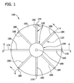
図1〜7は、結合構造体102を機械的に劈開させるための装置100を示す。図1〜7に示される結合構造体102は結合ウェハ対である。しかしながら、結合ウェハ対以外の構造体が、装置100を用いて劈開されてもよいことに留意すべきである。図3及び図4を参照すると、結合構造体102は、仮想線により示された劈開面140に沿って分離される。結合構造体102は、上面106(概して、第1表面)と、この反対側に設けられた下面108(概して、第2表面)と、を有する。結合構造体は、結合界面104に沿ってドナーウェハ112(概して、第2ウェハ)と結合されたハンドルウェハ110(概して、第1ウェハ)を含む。ドナーウェハ112内における劈開面140と結合界面104との間の距離は、明確のため、誇張されている。さらに、他の実施の形態では、ハンドルウェハ110の一部とドナーウェハ112とを入れ替えてもよく、これによりハンドルウェハがドナーウェハの下に配置されることとなる。
1-7 show an
図5及び6に示されているように、ドナーウェハ112及びハンドルウェハ110は、それらの周辺端面(周辺端部)において面取りされている(are beveled)。ウェハの周辺端面は、様々な外形(例えば、丸形状、弾丸形状(bulleted))を有していてもよいことに留意すべきである。本明細書において使用されているように、”面取りされた”との用語は、端面がウェハのフロント表面及びバック表面に対して実質的に垂直でなく、1以上のテイパー状端面を有する形状を意味するが、限定の意味に解釈すべきではない。さらに、本明細書において使用されているように、”テイパー状端面”とは、単に、フロント表面及びバック表面に対して平行でなく、端面の、ウェハの中心から最も離れた部分に向かって上方向若しくは下方向に傾斜している、ウェハ端部における表面を意味することに留意すべきである。さらに、そのような”テイパー状端面”は、直線状若しくは弓状であってもよく、直線状部分及び弓状部分の両方を含んでいてもよい。
As shown in FIGS. 5 and 6, the
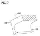
また、図5及び6に示すように、ドナーウェハ112及びハンドルウェハ110は、丸い端面を有する。ドナーウェハ112の端面は、第1部分148を有し、ハンドルウェハ110の端面は、第2部分152を有し、第1部分は、第2部分と対向して配置され、それにより、2つの端面間に凹部144が形成されている。概して、第1部分148及び第2部分152は、ウェハのテイパー状端面であり、当該端面は、結合ウェハ対の位置(orientation)に依存して、上方向若しくは下方向にテイパーが形成されている。図5及び6に示すように、ドナーウェハ112は、テイパー状端面146(同義的に”上方向にテイパー形成された端面”)を有し、これは、結合構造体の下面108から、端面の、ウェハの中心から最も離れた部分154(若しくは丸い端面の”点”)に向かって上方向に傾斜している。ドナーウェハ112は、また、端面148(同義的に”下方向にテイパー形成された端面”若しくは上述した”第1部分”)を含み、これは、界面104から、端面の最も外側の部分154まで下方向に傾斜している。ドナーウェハ112と同様に、ハンドルウェハ110は、ハンドルウェハの端面の最も外側の部分156まで傾斜した、上方向にテイパー形成された端面152(若しくは、上述した”第2部分”)、及び、ハンドルウェハ110の端面の最も外側の部分156まで傾斜した、下方向にテイパー形成された端面150を有する。ドナーウェハ112の下方向傾斜端面148及びハンドルウェハ110の上方向傾斜端面152により、2つの端面間に凹部144が形成されている。
Further, as shown in FIGS. 5 and 6, the
図1〜4に示すように、装置100は、ハンドルウェハ110を解放可能に固定する複数の第1クランプ170(若しくは”上側クランプ”)と、ドナーウェハ112を解放可能に固定する複数の第2クランプ184と、を備える。クランプ170、184は、第1アーム160及び第2アーム166にそれぞれ設けられている。第1アーム160は、第1中央ディスク190から延在し、第2アーム166は、第2中央ディスク192から延在する。第1中央ディスク190は、結合構造体102に対して第1クランプ170を適切に配置するため、当該結合構造体102の上面106に接触していてもよい。同様に、第2中央ディスク192は、第2クランプ184を配置することを助力してもよい。第1クランプ170、第1アーム160、第1中央ディスク190は併せて第1把持部材120(図1)を形成し、第2クランプ184、第2アーム184、第2中央ディスク192は併せて第2把持部材122(図4)を形成する。
As shown in FIGS. 1-4, the
図1に示すように、第1把持部材120は、4つのアーム160と、4つのクランプ170とを有し、また、第2把持部材122は、4つのアーム166と、4つのクランプ184とを有する。しかしながら、当該装置100の各部材120、122は、上記に制限されることなく、これより多い若しくは少ないアーム及びクランプを有していてもよいことに留意すべきである。いくつかの実施の形態において、装置100は、アームを有せず、むしろ、図8〜10に示され以下に記載された各ウェハを把持するための環状部材を有していてもよい。
As shown in FIG. 1, the first gripping
各第1クランプ170は、ハンドルウェハ110の上方向にテイパー形成された端面152に接触する表面130(図3及び図5)を有する。同様に、各第2クランプ184は、ドナーウェハ112の下方向にテイパー形成された端面148に接触する表面130(図4及び図6)を有する。図7においてさらに詳細に示すように、第1クランプ170の端面は、湾曲した形状を有し、アームの表面130が凹部144に入りハンドルウェハ110の上方向にテイパー形成された端面152に接触する(図5)。これに関して、”湾曲した”との用語は、限定の意味に解釈すべきではなく、アームが概して当該アームの他の部分に対してその方位角(angular direction)を変化させ、方向の1以上の緩やかな変化を含む(例えば、その長さ方向においてアームが1以上の角度を形成する)ようなプロファイルを意味する。
Each
180°の曲率(curvature)を有する第1クランプ170が示されているが、アームが結合構造体の中心から延在していない実施の形態等の他の実施の形態においては、クランプ180は180°以外の曲率を有していてもよい。例えば、アーム160が、結合構造体のフロント表面及びバック表面に対して垂直であり、クランプ170が、凹部144に向かって約90°屈曲しその表面130がテイパー形成された端面152に接触していてもよい。いくつかの実施の形態において、クランプ170は、アームが図7に示すアームのように反対方向から延在する実施の形態等のような湾曲した外形を有しない。この点に関し、第2クランプ184は、第1クランプ170と同様の形状及び/又は寸法を有していてもよい。しかしながら、第2クランプ184は、第1クランプ170と対称に置かれており、第2クランプ184は、ドナーウェハ112を把持することができる(すなわち、クランプ184は、凹部144(図5)に向かって、下方向ではなく、上方向に湾曲している)。クランプ170、184は、これに制限される訳ではなく、他の形状及び/又は寸法(例えば、互いに異なる)を有していてもよい。
Although a
図7に示すように、第1クランプ170は、結合構造体102のハンドルウェハ110に接触する表面130である端面を形成するため湾曲する(converge)。しかしながら、他の実施の形態では、表面130は、また、幅を有していてもよく(すなわち、表面は端部というより矩形若しくは四角形であってもよい)、又は、当該表面に接触する特異点(singular point)であってもよい。さらに、表面130は、弓状であってもよく、任意ではあるが、ハンドルウェハと表面130との間の接点を増加させるため、ハンドルウェハのテイパー状端面を補完する形状を有していてもよい。第2クランプ184の表面130は、第1クランプ170の表面130に関して上述した形状を有していてもよい。
As shown in FIG. 7, the
結合構造体102を分離するため、第1把持部材120及び/又は第2把持部材122は、その結合構造体を把持する。結合構造体102が把持される前、ロボット手段により、若しくは、把持部材120、122のうち一以上を用いることにより、結合構造体102を所定の位置に移動させてもよい。劈開前、他の把持部材が当該構造体を把持する。結合構造体102は、第1把持部材120の一部を構成する若しくは第1把持部材120に取り付けられている第1アクチュエータ(不図示)を用い部材120の1以上のアーム160を伸張及び収縮させることにより第1把持部材120によって把持されてもよい。同様に、結合構造体102は、第2把持部材122に取り付けられ若しくは第2把持部材122の一部を構成し第2把持部材122の1以上のアーム166を伸張及び収縮させる第2アクチュエータ(不図示)を用いることにより第2把持部材122によって把持される。第1把持部材120のアーム160及び第2把持部材122のアーム166の動作は、例えば、空気圧式アクチュエータ、油圧式アクチュエータ、若しくは、機械式アクチュエータを含む、当該技術分野における当業者に知られた任意の方法により行ってもよい。
In order to separate the
結合構造体102が第1把持部材120及び第2把持部材122により把持された後、第1把持部材120と第2把持部材122の一方若しくは両方に力を加えて、劈開面140に沿って結合構造体102を分離する。その際、アクチュエータ(不図示)が、第1把持部材120に取り付けられていてもよい。このアクチュエータにより、第1把持部材120が、ハンドルウェハ110に上方向の力を加えて当該構造体を分離させる。これに替えて、若しくは、これに加重して、第2把持部材122が、ドナーウェハ112に下方向の力を加えるように動作可能であるアクチュエータ(同じものでもよいし若しくは異なるアクチュエータでもよい)を第2把持部材122に取り付けてもよい。アクチュエータは、シャフト180、182に取り付けてもよいし、若しくは、把持部材120、122の他の部分に取り付けてもよい。第1把持部材120及び第2把持部材122の一方のみが、結合構造体の分離に用いられる力を与えるように作動する必要があるが、他のクランプは静止ポジションに維持してもよいことに留意すべきである。しかしながら、いくつかの実施の形態では、第1把持部材120及び第2把持部材122の両方が作動する。
After the
劈開プロセスは、結合構造体102に力を及ぼすブレード(不図示)を使用することにより開始してもよい。当該ブレードは、ハンドルウェハ110とドナーウェハ112との間に形成された凹部144に挿入され、結合構造体端面に力を加える。当該力により、劈開面140に沿った劈開が開始される。把持部材120、122の一方、若しくは両方により与えられる力と組み合わされるこの劈開により、結合構造体は劈開面140に沿って劈開され分離されることとなる。ブレードは、アクチュエータ(不図示)若しくは他の適切な機構により横方向に移動可能である。
The cleavage process may be initiated by using a blade (not shown) that exerts a force on the
本開示の及び図8〜10に示されたいくつかの実施の形態において、複数のアームを有するのではなく、把持部材は、結合構造体を少なくとも部分的に覆う1以上の環状部材を含んでいてもよい。図8に示すように、第1把持部材120は、第1環状部材194及び第2環状部材196を含み、結合構造体のハンドルウェハ110を把持する。第2把持部材122(図10)は、また、ドナーウェハ112を把持するための第1環状部材172及び第2環状部材188を有していてもよい。
In some embodiments of the present disclosure and illustrated in FIGS. 8-10, rather than having a plurality of arms, the gripping member includes one or more annular members that at least partially cover the coupling structure. May be. As shown in FIG. 8, the first holding
第1把持部材120の第1環状部材194及び第2環状部材196は、それぞれ、ハンドルウェハ110の上方向にテイパー形成された第1の端面に接触する表面130(図10)を有する。同様に、第1環状部材172及び第2環状部材188は、ドナーウェハ112の下方向にテイパー形成された端面に接触する表面130を備える。図8において矢印により示されているように、環状部材194、196は、その端面においてハンドルウェハ110に接触するように作動する(図9)。第2把持部材122の環状部材172、188は、同様に作動してもよい。ハンドルウェハ及びドナーウェハが一旦把持されると、第1把持部材120及び/又は第2把持部材122を作動させて反対方向の力を加えて結合構造体を劈開させる。
The first
第1把持部材120及び第2把持部材122の環状部材は、ハンドルウェハ110及びドナーウェハ112が、それらのそれぞれの周辺端面において連続的に接触するように、配置される必要はないことに留意すべきである。環状部材は、周辺端面の分離された部分に接触してもよい(すなわち、環状部材は、把持部材が2つの環状部材を有する場合、結合構造体の外周の半分未満の長さを有していてもよい)。これに制限される訳ではないが、さらに、各把持部材は、2以上の把持部材を有していてもよい。
It should be noted that the annular members of the first gripping
いくつかの実施の形態において、把持部材の一方若しくは両方は、劈開後ドナーウェハ及び/又はハンドルウェハが把持され解放されることを可能とするため、把持部材により直径を変化させることができる作動端面を有する一の環状部材から構成される(すなわち、把持部材は、連続するアニュラスである)。図11に例示された把持部材120が示されている。把持部材120は、動作するリップ176を含む。これは、作動時、把持部材の内径Dを変化させる1以上の動作部分108を有していてもよい。当該把持部材は、図8〜10に示された把持部材120、122のように半径方向に移動するのではなく、結合構造体に関して軸方向に移動し、結合構造体を把持する(当該結合構造体の上若しくは下から結合構造体に近づく)。
In some embodiments, one or both of the gripping members have an operating end surface that can be changed in diameter by the gripping member to allow the donor wafer and / or handle wafer to be gripped and released after cleaving. (I.e., the gripping member is a continuous annulus). The gripping
任意の特定の理論に拘泥される訳ではないが、従前のシステムにしたがって製造された構造体(例えば、SOI構造体)のいくつかの層における不均一の厚さ及び/又は不均一の粗さの変動が、結合構造体の表面に加えられる局在応力により引き起こされた。本明細書において記載された実施の形態は、ウェハ端部において力を加えることにより、上記問題を減少させ若しくは排除し、それにより、結果として得られるデバイスレイヤーにおいて厚さ及び/又は粗さの変動を減少させ若しくは排除する。 While not being bound by any particular theory, non-uniform thickness and / or non-uniform roughness in several layers of structures (eg, SOI structures) manufactured according to previous systems Variation was caused by localized stress applied to the surface of the bonded structure. The embodiments described herein reduce or eliminate the above problem by applying force at the wafer edge, thereby resulting in thickness and / or roughness variations in the resulting device layer. Is reduced or eliminated.
本開示のプロセスを、以下の実施例によりさらに説明する。これらの実施例は、限定の意味に解すべきではない。
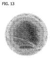
実施例1:吸引カップを使用して劈開されたSOI構造体のアキュマップ(登録商標)イメージと、ウェハ端面において反対方向の力を加えることにより劈開されたSOI構造体のアキュマップ(登録商標)イメージとの比較
The process of the present disclosure is further illustrated by the following examples. These examples should not be construed in a limiting sense.
Example 1: Accumap® image of SOI structure cleaved using a suction cup and Accumap® of SOI structure cleaved by applying an opposite direction force on the wafer edge. Comparison with image
結果として得られるSOI構造体からドナーウェハを分離するために吸引カップを使用する従来のプロセスにより結合ウェハ対を劈開した。劈開は、劈開ブレードを用いて開始した。また、第2SOI構造体は、劈開が劈開ブレードにより開始された後、結合構造体に上方向及び下方向の力を加えることにより作製した。 The bonded wafer pair was cleaved by a conventional process using a suction cup to separate the donor wafer from the resulting SOI structure. Cleavage was initiated using a cleaving blade. The second SOI structure was fabricated by applying upward and downward forces to the bonded structure after cleavage was initiated by the cleavage blade.
ウェハを劈開してSOI構造体を製造した後、デバイスレイヤーの構造体を撮像して、アキュマップ(登録商標)イメージ(アキュマップ(登録商標)3220;ADE)を生成した。吸引カップを使用する従来の方法により劈開されたSOI構造体から生成されたイメージを図12に示す。結合ウェハ端面において反対方向の力を加えることにより劈開されたSOI構造体から生成されたイメージを図13に示す。図12から分かるように、劈開の間吸引カップを用いて作製されたSOI構造体には、底部に強い劈開削痕(striation)があった(イメージの左端及び右端)。図13のSOI構造体は、より対称的であり、厚さの均一性がより大きい。 After the SOI structure was manufactured by cleaving the wafer, the structure of the device layer was imaged to generate an AccuMap (registered trademark) image (Accumap (registered trademark) 3220; ADE). An image generated from an SOI structure cleaved by a conventional method using a suction cup is shown in FIG. An image generated from an SOI structure cleaved by applying a force in the opposite direction at the bonded wafer end face is shown in FIG. As can be seen from FIG. 12, the SOI structure made with a suction cup during cleavage had strong cleavage striations at the bottom (left and right edges of the image). The SOI structure of FIG. 13 is more symmetric and has greater thickness uniformity.
本開示及びその実施の形態の構成要素を説明する際、冠詞”1つの(a)”、”1つの(an)”、”その(the)”、及び、”前述の(said)”は、1以上の構成要素が存在することを意味することを意図している。用語”含む(comprising)”、”包含する(including)”、”含有する(containing)”、及び、”有する(having)”は、包括的であることを意図し、列挙された構成要素以外の付加的な構成要素が存在しうることを意味することを意図している。特定の方向(例えば、”上部”、”下部”、”側部”等)を示す用語を使用することは、記載上の便宜のためであり、記載された事項の任意の特定の方向を要求する訳ではない。 In describing the components of the present disclosure and the embodiments thereof, the articles “one (a)”, “one (an)”, “the (the)”, and “the above” (said) are: It is intended to mean that one or more components are present. The terms “comprising”, “including”, “containing”, and “having” are intended to be inclusive and other than the listed components. It is intended to mean that additional components may be present. The use of terms that refer to a specific direction (eg, “top”, “bottom”, “side”, etc.) is for convenience of description and requires any specific direction of the items described Not to do.
本開示の技術的範囲から逸脱することなく上記構成及び方法において様々な変更を行うことができるため、上記記載に含まれ添付の図面に示された全ての事項は、限定ではなく、例示と解釈すべきであることを意図している。
本明細書の開示内容は、以下の態様を含み得る。
(態様1)
第1ウェハと第2ウェハとを含む結合ウェハ構造体を劈開させるための装置であって、前記第1ウェハは、第1部分を含む周辺端面を有し、前記第2ウェハは、第2部分を含む周辺端面を有し、前記第1部分は、前記第2部分と対向して配置され、
当該装置は、
第1アームと、
前記第1アームに設けられ、前記第1ウェハの周辺端面の第1部分に接触する表面を有する第1クランプと、
第2アームと、
前記第2アームに設けられ、前記第2ウェハの周辺端面の第2部分に接触する表面を有する第2クランプと、を備える装置。
(態様2)
前記第1アームと同様の複数のアームと、各アームに設けられた、前記第1クランプと同様のクランプと、をさらに備え、
前記第2アームと同様の複数のアームと、各アームに設けられた、前記第2クランプと同様のクランプと、をさらに備える態様1記載の装置。
(態様3)
前記第1ウェハを固定及び解放するために少なくとも前記第1クランプを外側へ移動させ(または伸ばし)及び内側へ移動させる(または引き込ませる)第1アクチュエータと、
前記第2ウェハを固定及び解放するために少なくとも1つの前記第2クランプを外側へ移動させ(または伸ばし)及び内側へ移動させる(または引き込ませる)第2アクチュエータと、をさらに備える態様2記載の装置。
(態様4)
前記第1クランプに取り付けられたアクチュエータをさらに備え、
前記アクチュエータの作動時、前記第1クランプは、前記第1ウェハに上方向の力を付与し、結合ウェハ構造体を劈開させる態様1〜3のいずれかに記載の装置。
(態様5)
前記第2クランプに取り付けられたアクチュエータをさらに備え、
前記アクチュエータの作動時、前記第2クランプは、前記第2ウェハに下方向の力を付与し、結合ウェハ構造体を劈開させる態様1〜4のいずれかに記載の装置。
(態様6)
前記第1クランプは、前記第1ウェハの周辺端面の第1部分に対して相補的な形状を有する端面を備え、
前記端面は、前記第1ウェハの周辺端面の第1部分に接触する表面を含む態様1〜4のいずれかに記載の装置。
(態様7)
前記第2クランプは、前記第2ウェハの周辺端面の第2部分に対して相補的な形状を有する端面を備え、
前記端面は、前記第2ウェハの周辺端面の第2部分に接触する表面を含む態様1〜4のいずれかに記載の装置。
(態様8)
第1ウェハと第2ウェハとを含む結合ウェハ構造体の劈開方法であって、前記第1ウェハは、第1部分を含む周辺端面を有し、前記第2ウェハは、第2部分を含む周辺端面を有し、前記第1部分は、前記第2部分と対向して配置され、
当該方法は、
前記第1ウェハの周辺端面の第1部分に、第1アームに設けられた第1クランプの表面を接触させることと、
前記第2ウェハの周辺端面の第2部分に、第2アームに設けられた第2クランプの表面を接触させることと、
(1)前記第1クランプを上方向に作動させることにより前記第1ウェハに対して上方向の力を付与すること、若しくは、(2)前記第2クランプを下方向に作動させることにより前記第2ウェハに対して下方向の力を付与すること、の少なくとも一方により、前記結合ウェハ構造体を劈開させること、を含む方法。
(態様9)
前記結合ウェハ対の劈開を開始するため、前記第1ウェハと前記第2ウェハとの間にブレードを挿入することをさらに含む態様8記載の方法。
(態様10)
前記第1アームと同様のアームに設けられた、前記第1クランプと同様の複数のクランプの表面が、前記第1ウェハの周辺端面の第1部分と接触する態様8又は9に記載の方法。
(態様11)
前記第2アームと同様のアームに設けられた、前記第2クランプと同様の複数のクランプの表面が、前記第2ウェハの周辺端面の第2部分と接触する態様8〜10のいずれかに記載の方法。
(態様12)
少なくとも第1クランプを外側へ移動(または伸ばして)及び内側へ移動させて(または引き込ませて)前記第1ウェハを固定するために、少なくとも前記第1クランプを作動させることと、
少なくとも第2クランプを外側へ移動(または伸ばして)及び内側へ移動させて(または引き込ませて)前記第2ウェハを固定するために、少なくとも前記第2クランプを作動させることと、
少なくとも第1クランプを外側へ移動(または伸ばして)及び内側へ移動させて(または引き込ませて)前記第1ウェハの少なくとも一部を解放するために、少なくとも前記第1クランプを作動させることと、
少なくとも第2クランプを外側へ移動(または伸ばして)及び内側へ移動させて(または引き込ませて)前記第2ウェハの少なくとも一部を解放するために、少なくとも前記第2クランプを作動させることと、を含む態様8〜11のいずれかに記載の方法。
(態様13)
前記第1ウェハに上方向の力を付与して前記結合ウェハ構造体を劈開させるために、前記第1クランプを作動させることを含む態様8〜12のいずれかに記載の方法。
(態様14)
前記第2ウェハに下方向の力を付与して前記結合ウェハ構造体を劈開させるために、前記第2クランプを作動させることを含む態様8〜13のいずれかに記載の方法。
(態様15)
前記第1クランプは、前記第1ウェハの周辺端面の第1部分に対して相補的な形状を有する端面を備え、
前記端面は、前記第1ウェハの周辺端面の第1部分に接触する表面を含む態様8〜14のいずれかに記載の方法。
(態様16)
前記第2クランプは、前記第2ウェハの周辺端面の第2部分に対して相補的な形状を有する端面を備え、
前記端面は、前記第2ウェハの周辺端面の第2部分に接触する表面を含む態様8〜15のいずれかに記載の方法。
(態様17)
第1ウェハと第2ウェハとを含む結合ウェハ構造体を劈開させるための装置であって、前記第1ウェハは、第1部分を含む周辺端面を有し、前記第2ウェハは、第2部分を含む周辺端面を有し、前記第1部分は、前記第2部分と対向して配置され、
当該装置は、
前記第1ウェハの周辺端面の第1部分に接触する表面を有する1以上の環状部材を備える第1把持部材と、
前記第2ウェハの周辺端面の第2部分に接触する表面を有する1以上の環状部材を備える第2把持部材と、を備える装置。
(態様18)
前記第1把持部材の1以上の環状部材は、前記第1ウェハの周辺端面の第1部分と連続的に接触する態様17記載の装置。
(態様19)
前記第2把持部材の1以上の環状部材は、前記第2ウェハの周辺端面の第2部分と連続的に接触する態様17記載の装置。
(態様20)
前記第1把持部材は、1つの環状部材を備え、
前記環状部材は、前記第1ウェハを把持及び解放する作動端面を有する態様17〜19のいずれかに記載の装置。
(態様21)
前記第2把持部材は、1つの環状部材を備え、
前記環状部材は、前記第2ウェハを把持及び解放する作動端面を有する態様17〜20のいずれかに記載の装置。
(態様22)
前記第1把持部材に取り付けられたアクチュエータをさらに備え、
前記アクチュエータの作動時、前記第1把持部材は、前記第1ウェハに上方向の力を付与し、結合ウェハ構造体を劈開させる態様17〜21のいずれかに記載の装置。
(態様23)
前記第2把持部材に取り付けられたアクチュエータをさらに備え、
前記アクチュエータの作動時、前記第2把持部材は、前記第2ウェハに上方向の力を付与し、結合ウェハ構造体を劈開させる態様17〜22のいずれかに記載の装置。
(態様24)
第1ウェハと第2ウェハとを含む結合ウェハ構造体の劈開方法であって、前記第1ウェハは、第1部分を含む周辺端面を有し、前記第2ウェハは、第2部分を含む周辺端面を有し、前記第1部分は、前記第2部分と対向して配置され、
当該方法は、
前記第1ウェハの周辺端面の第1部分に、第1把持部材の環状部材の表面を接触させることと、
前記第2ウェハの周辺端面の第2部分に、第2把持部材の環状部材の表面を接触させることと、
(1)前記第1把持部材を上方向に作動させることにより前記第1ウェハに対して上方向の力を付与すること、若しくは、(2)前記第2把持部材を下方向に作動させることにより前記第2ウェハに対して下方向の力を付与することの少なくとも一方により、前記結合ウェハ構造体を劈開させること、を含む方法。
(態様25)
前記結合ウェハ対の劈開を開始するため、前記第1ウェハと前記第2ウェハとの間にブレードを挿入することをさらに含む態様24記載の方法。
(態様26)
前記第1ウェハに上方向の力を付与して前記結合ウェハ構造体を劈開させるために、前記第1把持部材を作動させることを含む態様24又は25記載の方法。
(態様27)
前記第2ウェハに下方向の力を付与して前記結合ウェハ構造体を劈開させるために、前記第2把持部材を作動させることを含む態様24〜26のいずれかに記載の方法。
(態様28)
前記第1把持部材の1以上の環状部材が、前記第1ウェハの周辺部材の第1部分と連続的に接触する態様24〜27のいずれかに記載の方法。
(態様29)
前記第2把持部材の1以上の環状部材が、前記第2ウェハの周辺部材の第2部分と連続的に接触する態様24〜28のいずれかに記載の方法。
(態様30)
前記第1把持部材は、1つの環状部材を備え、
前記環状部材は、作動端面を有し、
当該方法は、
前記第1ウェハを把持及び解放するため、前記端面を作動させることを含む態様24〜29のいずれかに記載の方法。
(態様31)
前記第2把持部材は、1つの環状部材を備え、
前記環状部材は、作動端面を有し、
当該方法は、
前記第2ウェハを把持及び解放するため、前記端面を作動させることを含む態様24〜30のいずれかに記載の方法。
Since various modifications can be made in the above configurations and methods without departing from the technical scope of the present disclosure, all matters contained in the above description and shown in the accompanying drawings are illustrative and not restrictive. Intended to be.
The disclosure of the present specification may include the following aspects.
(Aspect 1)
An apparatus for cleaving a combined wafer structure including a first wafer and a second wafer, wherein the first wafer has a peripheral end surface including a first portion, and the second wafer is a second portion. The first portion is disposed to face the second portion, and
The device is
A first arm;
A first clamp having a surface provided on the first arm and in contact with a first portion of a peripheral end surface of the first wafer;
A second arm;
A second clamp having a surface provided on the second arm and having a surface in contact with a second portion of a peripheral end surface of the second wafer.
(Aspect 2)
A plurality of arms similar to the first arm, and a clamp similar to the first clamp provided in each arm;
The apparatus according to aspect 1, further comprising: a plurality of arms similar to the second arm; and a clamp similar to the second clamp provided on each arm.
(Aspect 3)
A first actuator that moves (or extends) and moves (or retracts) at least the first clamp at least to clamp and release the first wafer;
The apparatus of aspect 2, further comprising: a second actuator that moves (or stretches) and moves (or retracts) at least one of the second clamps outward to fix and release the second wafer. .
(Aspect 4)
An actuator attached to the first clamp;
The apparatus according to any one of aspects 1 to 3, wherein, when the actuator is operated, the first clamp applies an upward force to the first wafer to cleave the bonded wafer structure.
(Aspect 5)
An actuator attached to the second clamp;
The apparatus according to any one of aspects 1 to 4, wherein, when the actuator is actuated, the second clamp applies a downward force to the second wafer to cleave the bonded wafer structure.
(Aspect 6)
The first clamp includes an end surface having a shape complementary to a first portion of a peripheral end surface of the first wafer;
The apparatus according to any one of aspects 1 to 4, wherein the end face includes a surface that contacts a first portion of a peripheral end face of the first wafer.
(Aspect 7)
The second clamp includes an end surface having a shape complementary to a second portion of a peripheral end surface of the second wafer;
The said end surface is an apparatus in any one of the aspects 1-4 containing the surface which contacts the 2nd part of the peripheral end surface of the said 2nd wafer.
(Aspect 8)
A method for cleaving a combined wafer structure including a first wafer and a second wafer, wherein the first wafer has a peripheral end surface including a first portion, and the second wafer includes a second portion. Having an end face, the first portion is disposed opposite the second portion;
The method is
Bringing the first portion of the peripheral edge of the first wafer into contact with the surface of the first clamp provided on the first arm;
Bringing the second portion of the peripheral edge of the second wafer into contact with the surface of the second clamp provided on the second arm;
(1) An upward force is applied to the first wafer by operating the first clamp upward, or (2) the first clamp is operated by operating the second clamp downward. Cleaving the combined wafer structure by at least one of applying a downward force to the two wafers.
(Aspect 9)
9. The method of aspect 8, further comprising inserting a blade between the first wafer and the second wafer to initiate cleavage of the bonded wafer pair.
(Aspect 10)
The method according to claim 8 or 9, wherein surfaces of a plurality of clamps similar to the first clamp provided on an arm similar to the first arm are in contact with a first portion of a peripheral end surface of the first wafer.
(Aspect 11)
The surface of the some clamp similar to the said 2nd clamp provided in the arm similar to the said 2nd arm is in any one of the aspects 8-10 which contact the 2nd part of the peripheral end surface of the said 2nd wafer. the method of.
(Aspect 12)
Activating at least the first clamp to secure the first wafer by moving (or extending) and moving (or retracting) at least the first clamp outwardly;
Activating at least the second clamp to secure the second wafer by moving (or extending) and moving (or retracting) at least the second clamp outward;
Activating at least the first clamp to release at least a portion of the first wafer by moving (or extending) and moving (or retracting) at least the first clamp at least outwardly;
Activating at least the second clamp to release at least a portion of the second wafer by moving (or extending) and moving (or retracting) at least the second clamp outwardly; The method in any one of aspect 8-11 containing these.
(Aspect 13)
13. A method according to any of aspects 8-12, including actuating the first clamp to apply an upward force to the first wafer to cleave the bonded wafer structure.
(Aspect 14)
14. The method according to any of aspects 8-13, including actuating the second clamp to apply a downward force to the second wafer to cleave the bonded wafer structure.
(Aspect 15)
The first clamp includes an end surface having a shape complementary to a first portion of a peripheral end surface of the first wafer;
The method according to any one of aspects 8 to 14, wherein the end face includes a surface that contacts a first portion of a peripheral end face of the first wafer.
(Aspect 16)
The second clamp includes an end surface having a shape complementary to a second portion of a peripheral end surface of the second wafer;
The method according to any one of aspects 8 to 15, wherein the end surface includes a surface that contacts a second portion of a peripheral end surface of the second wafer.
(Aspect 17)
An apparatus for cleaving a combined wafer structure including a first wafer and a second wafer, wherein the first wafer has a peripheral end surface including a first portion, and the second wafer is a second portion. The first portion is disposed to face the second portion, and
The device is
A first gripping member comprising one or more annular members having a surface in contact with a first portion of a peripheral end surface of the first wafer;
A second gripping member comprising one or more annular members having a surface in contact with a second portion of the peripheral end surface of the second wafer.
(Aspect 18)
The apparatus according to aspect 17, wherein the one or more annular members of the first gripping member are in continuous contact with the first portion of the peripheral end surface of the first wafer.
(Aspect 19)
The apparatus according to claim 17, wherein the one or more annular members of the second gripping member are in continuous contact with the second portion of the peripheral end surface of the second wafer.
(Aspect 20)
The first gripping member includes one annular member,
The apparatus according to any one of aspects 17 to 19, wherein the annular member has an operating end surface for gripping and releasing the first wafer.
(Aspect 21)
The second gripping member includes one annular member,
21. The apparatus according to any one of aspects 17 to 20, wherein the annular member has an operating end surface that grips and releases the second wafer.
(Aspect 22)
An actuator attached to the first gripping member;
The apparatus according to any one of aspects 17 to 21, wherein when the actuator is operated, the first gripping member applies an upward force to the first wafer to cleave the combined wafer structure.
(Aspect 23)
An actuator attached to the second gripping member;
The apparatus according to any one of aspects 17 to 22, wherein, when the actuator is operated, the second gripping member applies an upward force to the second wafer to cleave the combined wafer structure.
(Aspect 24)
A method for cleaving a combined wafer structure including a first wafer and a second wafer, wherein the first wafer has a peripheral end surface including a first portion, and the second wafer includes a second portion. Having an end face, the first portion is disposed opposite the second portion;
The method is
Bringing the surface of the annular member of the first gripping member into contact with the first portion of the peripheral end surface of the first wafer;
Bringing the surface of the annular member of the second gripping member into contact with the second portion of the peripheral end surface of the second wafer;
(1) By applying an upward force to the first wafer by operating the first gripping member upward, or (2) by operating the second gripping member downward. Cleaving the combined wafer structure by at least one of applying a downward force to the second wafer.
(Aspect 25)
25. The method of aspect 24, further comprising inserting a blade between the first wafer and the second wafer to initiate cleavage of the bonded wafer pair.
(Aspect 26)
26. The method of embodiment 24 or 25, comprising actuating the first gripping member to apply an upward force to the first wafer to cleave the combined wafer structure.
(Aspect 27)
27. A method according to any of aspects 24-26, comprising actuating the second gripping member to apply a downward force to the second wafer to cleave the combined wafer structure.
(Aspect 28)
28. A method according to any of aspects 24-27, wherein one or more annular members of the first gripping member are in continuous contact with a first portion of a peripheral member of the first wafer.
(Aspect 29)
29. A method according to any of aspects 24-28, wherein one or more annular members of the second gripping member are in continuous contact with a second portion of a peripheral member of the second wafer.
(Aspect 30)
The first gripping member includes one annular member,
The annular member has an operating end surface;
The method is
30. A method according to any of aspects 24-29, comprising actuating the end face to grip and release the first wafer.
(Aspect 31)
The second gripping member includes one annular member,
The annular member has an operating end surface;
The method is
31. A method according to any of aspects 24-30, comprising actuating the end face to grip and release the second wafer.
Claims (15)
当該装置は、
第1アームと、
前記第1アームに設けられ、前記第1ウェハの周辺端面の第1部分に接触する表面を有する第1クランプと、
第2アームと、
前記第2アームに設けられ、前記第2ウェハの周辺端面の第2部分に接触する表面を有する第2クランプと、を備える装置。 An apparatus for cleaving a combined wafer structure including a first wafer and a second wafer, wherein the first wafer has a peripheral end surface including a first portion, and the second wafer is a second portion. The first portion is disposed to face the second portion, and
The device is
A first arm;
A first clamp having a surface provided on the first arm and in contact with a first portion of a peripheral end surface of the first wafer;
A second arm;
A second clamp having a surface provided on the second arm and having a surface in contact with a second portion of a peripheral end surface of the second wafer.
前記第2アームと同様の複数のアームと、各アームに設けられた、前記第2クランプと同様のクランプと、をさらに備える請求項1記載の装置。 A plurality of arms similar to the first arm, and a clamp similar to the first clamp provided in each arm;
The apparatus according to claim 1, further comprising: a plurality of arms similar to the second arm; and a clamp similar to the second clamp provided on each arm.
前記第2ウェハを固定及び解放するために少なくとも1つの前記第2クランプを外側へ移動させ及び内側へ移動させる第2アクチュエータと、をさらに備える請求項2記載の装置。 A first actuator for moving at least the first clamp outward and inward to fix and release the first wafer;
3. The apparatus of claim 2, further comprising a second actuator that moves at least one of the second clamps outward and inward to secure and release the second wafer.
前記アクチュエータの作動時、前記第1クランプは、前記第1ウェハに上方向の力を付与し、結合ウェハ構造体を劈開させる請求項1〜3のいずれかに記載の装置。 An actuator attached to the first clamp;
The apparatus according to claim 1, wherein, when the actuator is actuated, the first clamp applies an upward force to the first wafer to cleave the bonded wafer structure.
当該方法は、
前記第1ウェハの周辺端面の第1部分に、第1アームに設けられた第1クランプの表面を接触させることと、
前記第2ウェハの周辺端面の第2部分に、第2アームに設けられた第2クランプの表面を接触させることと、
(1)前記第1クランプを上方向に作動させることにより前記第1ウェハに対して上方向の力を付与すること、若しくは、(2)前記第2クランプを下方向に作動させることにより前記第2ウェハに対して下方向の力を付与すること、の少なくとも一方により、前記結合ウェハ構造体を劈開させること、を含む方法。 A method for cleaving a combined wafer structure including a first wafer and a second wafer, wherein the first wafer has a peripheral end surface including a first portion, and the second wafer includes a second portion. Having an end face, the first portion is disposed opposite the second portion;
The method is
Bringing the first portion of the peripheral edge of the first wafer into contact with the surface of the first clamp provided on the first arm;
Bringing the second portion of the peripheral edge of the second wafer into contact with the surface of the second clamp provided on the second arm;
(1) An upward force is applied to the first wafer by operating the first clamp upward, or (2) the first clamp is operated by operating the second clamp downward. Cleaving the combined wafer structure by at least one of applying a downward force to the two wafers.
当該装置は、
前記第1ウェハの周辺端面の第1部分に接触する表面を有する1以上の環状部材を備える第1把持部材と、
前記第2ウェハの周辺端面の第2部分に接触する表面を有する1以上の環状部材を備える第2把持部材と、を備え、
前記第1把持部材の環状部材、または前記第2把持部材の環状部材が、ウェハを把持及び解放する作動端面を有している、
装置。 An apparatus for cleaving a combined wafer structure including a first wafer and a second wafer, wherein the first wafer has a peripheral end surface including a first portion, and the second wafer is a second portion. The first portion is disposed to face the second portion, and
The device is
A first gripping member comprising one or more annular members having a surface in contact with a first portion of a peripheral end surface of the first wafer;
A second gripping member comprising one or more annular members having a surface in contact with the second portion of the peripheral end surface of the second wafer ,
The annular member of the first holding member or the annular member of the second holding member has an operating end surface for holding and releasing the wafer.
apparatus.
前記環状部材は、前記第2ウェハを把持及び解放する作動端面を有する請求項7又は8に記載の装置。 The second gripping member includes one annular member,
The apparatus according to claim 7 or 8, wherein the annular member has an operating end face for gripping and releasing the second wafer.
前記アクチュエータの作動時、前記第1把持部材は、前記第1ウェハに上方向の力を付与し、結合ウェハ構造体を劈開させる請求項7〜9のいずれかに記載の装置。 An actuator attached to the first gripping member;
The apparatus according to any one of claims 7 to 9, wherein when the actuator is operated, the first gripping member applies an upward force to the first wafer to cleave the combined wafer structure.
当該方法は、
前記第1ウェハの周辺端面の第1部分に、第1把持部材の環状部材の表面を接触させることと、
前記第2ウェハの周辺端面の第2部分に、第2把持部材の環状部材の表面を接触させることと、
前記第1把持部材の環状部材、または前記第2把持部材の環状部材が作動端面を有しており、前記作動端面を作動させて、第1ウェハまたは第2ウェハを把持及び解放することと、
(1)前記第1把持部材を上方向に作動させることにより前記第1ウェハに対して上方向の力を付与すること、若しくは、(2)前記第2把持部材を下方向に作動させることにより前記第2ウェハに対して下方向の力を付与することの少なくとも一方により、前記結合ウェハ構造体を劈開させること、を含む方法。 A method for cleaving a combined wafer structure including a first wafer and a second wafer, wherein the first wafer has a peripheral end surface including a first portion, and the second wafer includes a second portion. Having an end face, the first portion is disposed opposite the second portion;
The method is
Bringing the surface of the annular member of the first gripping member into contact with the first portion of the peripheral end surface of the first wafer;
Bringing the surface of the annular member of the second gripping member into contact with the second portion of the peripheral end surface of the second wafer;
The annular member of the first gripping member or the annular member of the second gripping member has an operating end surface, and operating the operating end surface to grip and release the first wafer or the second wafer;
(1) By applying an upward force to the first wafer by operating the first gripping member upward, or (2) by operating the second gripping member downward. Cleaving the combined wafer structure by at least one of applying a downward force to the second wafer.
前記環状部材は、作動端面を有し、
当該方法は、
前記第1ウェハを把持及び解放するため、前記作動端面を作動させることを含む請求項11〜13のいずれかに記載の方法。 The first gripping member includes one annular member,
The annular member has an operating end surface;
The method is
14. A method according to any of claims 11 to 13, comprising actuating the working end face to grip and release the first wafer.
前記環状部材は、作動端面を有し、
当該方法は、
前記第2ウェハを把持及び解放するため、前記作動端面を作動させることを含む請求項11〜14のいずれかに記載の方法。 The second gripping member includes one annular member,
The annular member has an operating end surface;
The method is
15. A method according to any of claims 11 to 14, comprising actuating the working end face to grip and release the second wafer.
Applications Claiming Priority (3)
| Application Number | Priority Date | Filing Date | Title |
|---|---|---|---|
| US201161553447P | 2011-10-31 | 2011-10-31 | |
| US61/553,447 | 2011-10-31 | ||
| PCT/US2012/062194 WO2013066758A1 (en) | 2011-10-31 | 2012-10-26 | Clamping apparatus for cleaving a bonded wafer structure and methods for cleaving |
Publications (3)
| Publication Number | Publication Date |
|---|---|
| JP2014532992A JP2014532992A (en) | 2014-12-08 |
| JP2014532992A5 JP2014532992A5 (en) | 2015-12-03 |
| JP6167108B2 true JP6167108B2 (en) | 2017-07-19 |
Family
ID=47221551
Family Applications (1)
| Application Number | Title | Priority Date | Filing Date |
|---|---|---|---|
| JP2014539062A Active JP6167108B2 (en) | 2011-10-31 | 2012-10-26 | Fixing apparatus and cleavage method for cleaving a bonded wafer structure |
Country Status (7)
| Country | Link |
|---|---|
| US (3) | US9159596B2 (en) |
| EP (1) | EP2774176B1 (en) |
| JP (1) | JP6167108B2 (en) |
| KR (1) | KR102061359B1 (en) |
| CN (1) | CN104025277A (en) |
| TW (1) | TWI622119B (en) |
| WO (1) | WO2013066758A1 (en) |
Families Citing this family (13)
| Publication number | Priority date | Publication date | Assignee | Title |
|---|---|---|---|---|
| KR102061359B1 (en) * | 2011-10-31 | 2019-12-31 | 글로벌웨이퍼스 씨오., 엘티디. | Clamping apparatus for cleaving a bonded wafer structure and methods for cleaving |
| AT519840B1 (en) * | 2014-01-28 | 2019-04-15 | Ev Group E Thallner Gmbh | Apparatus and method for releasing a first substrate |
| CN104505363A (en) * | 2014-12-25 | 2015-04-08 | 苏州凯锝微电子有限公司 | Wafer clamping device |
| CN104701233B (en) * | 2015-03-10 | 2017-10-17 | 北京七星华创电子股份有限公司 | A kind of disk clamping device |
| WO2017026279A1 (en) * | 2015-08-11 | 2017-02-16 | 東京応化工業株式会社 | Support body separating device and support body separating method |
| US10272661B2 (en) | 2017-04-17 | 2019-04-30 | Taiwan Semiconductor Manufacturing Company, Ltd. | Pad removal device and method |
| EP3657537A1 (en) * | 2018-11-23 | 2020-05-27 | ATOTECH Deutschland GmbH | End effector for slab formed substrates |
| FR3093858B1 (en) * | 2019-03-15 | 2021-03-05 | Soitec Silicon On Insulator | Method of transferring a useful layer onto a support substrate |
| FR3093715B1 (en) * | 2019-03-15 | 2021-03-05 | Soitec Silicon On Insulator | Holding device for an assembly to be fractured |
| CN110640324B (en) * | 2019-09-02 | 2022-06-10 | 中芯集成电路(宁波)有限公司 | Wafer double-side manufacturing system |
| JP7309191B2 (en) * | 2019-11-06 | 2023-07-18 | 中村留精密工業株式会社 | Wafer splitter |
| JP7471862B2 (en) | 2020-02-27 | 2024-04-22 | キオクシア株式会社 | Bonding device and bonding method |
| JP7339905B2 (en) | 2020-03-13 | 2023-09-06 | キオクシア株式会社 | Bonding device and bonding method |
Family Cites Families (32)
| Publication number | Priority date | Publication date | Assignee | Title |
|---|---|---|---|---|
| SE369160B (en) * | 1972-12-21 | 1974-08-12 | Siporex Int Ab | |
| US5367762A (en) | 1992-12-23 | 1994-11-29 | Advanced Micro Devices, Inc. | Decapping machine for packaged integrated circuits |
| JP3408000B2 (en) | 1994-11-28 | 2003-05-19 | 菱電セミコンダクタシステムエンジニアリング株式会社 | Pellicle peeling method |
| JPH09263500A (en) | 1996-01-22 | 1997-10-07 | Komatsu Electron Metals Co Ltd | Jig for stripping stuck soi wafer |
| US6013563A (en) | 1997-05-12 | 2000-01-11 | Silicon Genesis Corporation | Controlled cleaning process |
| JPH115064A (en) * | 1997-06-16 | 1999-01-12 | Canon Inc | Separation device for sample and method thereof and production of board |
| EP0951068A1 (en) | 1998-04-17 | 1999-10-20 | Interuniversitair Micro-Elektronica Centrum Vzw | Method of fabrication of a microstructure having an inside cavity |
| US6672358B2 (en) * | 1998-11-06 | 2004-01-06 | Canon Kabushiki Kaisha | Sample processing system |
| JP3917313B2 (en) * | 1999-01-26 | 2007-05-23 | ローム株式会社 | Transfer jig for semiconductor manufacturing products |
| AU6905000A (en) | 1999-08-10 | 2001-03-05 | Silicon Genesis Corporation | A cleaving process to fabricate multilayered substrates using low implantation doses |
| US6221740B1 (en) | 1999-08-10 | 2001-04-24 | Silicon Genesis Corporation | Substrate cleaving tool and method |
| US6263941B1 (en) | 1999-08-10 | 2001-07-24 | Silicon Genesis Corporation | Nozzle for cleaving substrates |
| US6336787B1 (en) | 1999-10-07 | 2002-01-08 | Mosel Vitelic, Inc. | Method for transferring wafers in a semiconductor tape-peeling apparatus |
| TW508690B (en) | 1999-12-08 | 2002-11-01 | Canon Kk | Composite member separating method, thin film manufacturing method, and composite member separating apparatus |
| US6444082B1 (en) * | 2000-06-22 | 2002-09-03 | International Business Machines Corporation | Apparatus and method for removing a bonded lid from a substrate |
| JP2002050749A (en) * | 2000-07-31 | 2002-02-15 | Canon Inc | Method and device for separating composite member |
| US6491083B2 (en) | 2001-02-06 | 2002-12-10 | Anadigics, Inc. | Wafer demount receptacle for separation of thinned wafer from mounting carrier |
| FR2823373B1 (en) | 2001-04-10 | 2005-02-04 | Soitec Silicon On Insulator | DEVICE FOR CUTTING LAYER OF SUBSTRATE, AND ASSOCIATED METHOD |
| AT502233B1 (en) | 2001-06-07 | 2007-04-15 | Thallner Erich | Carrier detachment device aligns inner, near-edge surface of frame with semiconductor disk and bonds them to foil, before detaching disk from carrier |
| JP2003288028A (en) | 2001-12-25 | 2003-10-10 | Canon Inc | Method for disassembling image display apparatus, method for producing image display apparatus, method for producing support member, method for producing image display unit, method for producing working material, and image display apparatus |
| FR2834381B1 (en) | 2002-01-03 | 2004-02-27 | Soitec Silicon On Insulator | DEVICE FOR CUTTING A LAYER OF A SUBSTRATE, AND ASSOCIATED METHOD |
| TWI223371B (en) * | 2003-03-18 | 2004-11-01 | Taiwan Semiconductor Mfg | Chuck rotating and chuck roller apparatuses |
| JP4364535B2 (en) | 2003-03-27 | 2009-11-18 | シャープ株式会社 | Manufacturing method of semiconductor device |
| EP1662550B1 (en) | 2003-09-05 | 2019-12-04 | SUMCO Corporation | Method for producing soi wafer |
| JP2006135272A (en) | 2003-12-01 | 2006-05-25 | Tokyo Ohka Kogyo Co Ltd | Substrate support plate and peeling method of support plate |
| JP4995626B2 (en) * | 2007-04-27 | 2012-08-08 | 信越化学工業株式会社 | Manufacturing method of bonded substrate |
| JP2009154407A (en) * | 2007-12-27 | 2009-07-16 | Tdk Corp | Peeling apparatus, peeling method, and information recording medium manufacturing method |
| JP2010010207A (en) * | 2008-06-24 | 2010-01-14 | Tokyo Ohka Kogyo Co Ltd | Separating apparatus and separating method |
| JP5448860B2 (en) * | 2010-01-13 | 2014-03-19 | 東京応化工業株式会社 | Separation method and separation apparatus |
| US8845859B2 (en) | 2011-03-15 | 2014-09-30 | Sunedison Semiconductor Limited (Uen201334164H) | Systems and methods for cleaving a bonded wafer pair |
| KR102061359B1 (en) * | 2011-10-31 | 2019-12-31 | 글로벌웨이퍼스 씨오., 엘티디. | Clamping apparatus for cleaving a bonded wafer structure and methods for cleaving |
| SG2014013007A (en) * | 2011-12-22 | 2014-06-27 | Ev Group E Thallner Gmbh | Flexible substrate mount, device and method for detaching a first substrate |
-
2012
- 2012-10-26 KR KR1020147011610A patent/KR102061359B1/en active IP Right Grant
- 2012-10-26 CN CN201280053782.4A patent/CN104025277A/en active Pending
- 2012-10-26 JP JP2014539062A patent/JP6167108B2/en active Active
- 2012-10-26 EP EP12790726.9A patent/EP2774176B1/en active Active
- 2012-10-26 WO PCT/US2012/062194 patent/WO2013066758A1/en active Application Filing
- 2012-10-29 US US13/663,073 patent/US9159596B2/en active Active
- 2012-10-29 US US13/663,038 patent/US9165802B2/en active Active
- 2012-10-31 TW TW101140405A patent/TWI622119B/en active
-
2015
- 2015-09-04 US US14/845,327 patent/US9925755B2/en active Active
Also Published As
| Publication number | Publication date |
|---|---|
| KR102061359B1 (en) | 2019-12-31 |
| EP2774176A1 (en) | 2014-09-10 |
| US20130105538A1 (en) | 2013-05-02 |
| KR20140085477A (en) | 2014-07-07 |
| US9925755B2 (en) | 2018-03-27 |
| US9159596B2 (en) | 2015-10-13 |
| TWI622119B (en) | 2018-04-21 |
| CN104025277A (en) | 2014-09-03 |
| EP2774176B1 (en) | 2016-08-10 |
| US9165802B2 (en) | 2015-10-20 |
| WO2013066758A1 (en) | 2013-05-10 |
| US20150375495A1 (en) | 2015-12-31 |
| US20130105539A1 (en) | 2013-05-02 |
| JP2014532992A (en) | 2014-12-08 |
| TW201324676A (en) | 2013-06-16 |
Similar Documents
| Publication | Publication Date | Title |
|---|---|---|
| JP6167108B2 (en) | Fixing apparatus and cleavage method for cleaving a bonded wafer structure | |
| US6468879B1 (en) | Method and device for separating a plate of material, in particular semiconductor material, into two wafers | |
| KR101239282B1 (en) | Method and apparatus for removing a reversibly mounted device wafer from a carrier substrate | |
| US8845859B2 (en) | Systems and methods for cleaving a bonded wafer pair | |
| TW201139147A (en) | Process for fabricating a multilayer structure with trimming using thermo-mechanical effects | |
| EP2434533A1 (en) | Bonding process by molecular bonding with reduced overlay type misalignment | |
| JP2014532992A5 (en) | ||
| TWI648810B (en) | Apparatus and method for thin wafer transfer | |
| TW201005812A (en) | A method of assembling wafers by molecular bonding | |
| JP2015505164A (en) | Flexible substrate holding apparatus, apparatus and method for peeling first substrate | |
| JP5912117B2 (en) | Method for forming a film, for example, a single crystal film, on a polymer substrate | |
| TW201241955A (en) | Apparatus and a method for direct wafer bonding | |
| US20120186741A1 (en) | Apparatus for wafer-to-wafer bonding | |
| TWI833039B (en) | Cleave systems having spring members for cleaving a semiconductor structure and methods for cleaving such structures | |
| JP3656254B2 (en) | Method and apparatus for peeling adhesive wafer | |
| US9321636B2 (en) | Method for producing a substrate holder | |
| WO2014049414A1 (en) | Direct bonding process | |
| EP3772747B1 (en) | Positioning tool | |
| JP6469070B2 (en) | Method for peeling a first substrate from a second substrate and use of a flexible substrate holding device | |
| TW201935519A (en) | Detachable structure and detachment process using said structure | |
| TW201201993A (en) | Resin material removing method and apparatus thereof | |
| JP2012160660A (en) | Apparatus and method for semiconductor wafer breaking |
Legal Events
| Date | Code | Title | Description |
|---|---|---|---|
| A521 | Request for written amendment filed |
Free format text: JAPANESE INTERMEDIATE CODE: A523 Effective date: 20151014 |
|
| A621 | Written request for application examination |
Free format text: JAPANESE INTERMEDIATE CODE: A621 Effective date: 20151014 |
|
| RD04 | Notification of resignation of power of attorney |
Free format text: JAPANESE INTERMEDIATE CODE: A7424 Effective date: 20160216 |
|
| A977 | Report on retrieval |
Free format text: JAPANESE INTERMEDIATE CODE: A971007 Effective date: 20160916 |
|
| A131 | Notification of reasons for refusal |
Free format text: JAPANESE INTERMEDIATE CODE: A131 Effective date: 20160927 |
|
| A521 | Request for written amendment filed |
Free format text: JAPANESE INTERMEDIATE CODE: A523 Effective date: 20161220 |
|
| TRDD | Decision of grant or rejection written | ||
| A01 | Written decision to grant a patent or to grant a registration (utility model) |
Free format text: JAPANESE INTERMEDIATE CODE: A01 Effective date: 20170530 |
|
| A61 | First payment of annual fees (during grant procedure) |
Free format text: JAPANESE INTERMEDIATE CODE: A61 Effective date: 20170626 |
|
| R150 | Certificate of patent or registration of utility model |
Ref document number: 6167108 Country of ref document: JP Free format text: JAPANESE INTERMEDIATE CODE: R150 |
|
| S111 | Request for change of ownership or part of ownership |
Free format text: JAPANESE INTERMEDIATE CODE: R313113 |
|
| S531 | Written request for registration of change of domicile |
Free format text: JAPANESE INTERMEDIATE CODE: R313531 |
|
| S533 | Written request for registration of change of name |
Free format text: JAPANESE INTERMEDIATE CODE: R313533 |
|
| R350 | Written notification of registration of transfer |
Free format text: JAPANESE INTERMEDIATE CODE: R350 |
|
| R250 | Receipt of annual fees |
Free format text: JAPANESE INTERMEDIATE CODE: R250 |
|
| R250 | Receipt of annual fees |
Free format text: JAPANESE INTERMEDIATE CODE: R250 |
|
| R250 | Receipt of annual fees |
Free format text: JAPANESE INTERMEDIATE CODE: R250 |
|
| R250 | Receipt of annual fees |
Free format text: JAPANESE INTERMEDIATE CODE: R250 |