JP6166516B2 - Imprint apparatus, imprint method, and article manufacturing method - Google Patents

Imprint apparatus, imprint method, and article manufacturing method Download PDF

Info

Publication number
JP6166516B2
JP6166516B2 JP2012159078A JP2012159078A JP6166516B2 JP 6166516 B2 JP6166516 B2 JP 6166516B2 JP 2012159078 A JP2012159078 A JP 2012159078A JP 2012159078 A JP2012159078 A JP 2012159078A JP 6166516 B2 JP6166516 B2 JP 6166516B2
Authority
JP
Japan
Prior art keywords
substrate
mold
unit
imprint
distance
Prior art date
Legal status (The legal status is an assumption and is not a legal conclusion. Google has not performed a legal analysis and makes no representation as to the accuracy of the status listed.)
Active
Application number
JP2012159078A
Other languages
Japanese (ja)
Other versions
JP2014022527A5 (en
JP2014022527A (en
Inventor
木村 淳
淳 木村
Current Assignee (The listed assignees may be inaccurate. Google has not performed a legal analysis and makes no representation or warranty as to the accuracy of the list.)
Canon Inc
Original Assignee
Canon Inc
Priority date (The priority date is an assumption and is not a legal conclusion. Google has not performed a legal analysis and makes no representation as to the accuracy of the date listed.)
Filing date
Publication date
Application filed by Canon Inc filed Critical Canon Inc
Priority to JP2012159078A priority Critical patent/JP6166516B2/en
Publication of JP2014022527A publication Critical patent/JP2014022527A/en
Publication of JP2014022527A5 publication Critical patent/JP2014022527A5/ja
Application granted granted Critical
Publication of JP6166516B2 publication Critical patent/JP6166516B2/en
Active legal-status Critical Current
Anticipated expiration legal-status Critical

Links

Images

Landscapes

  • Shaping Of Tube Ends By Bending Or Straightening (AREA)
  • Exposure Of Semiconductors, Excluding Electron Or Ion Beam Exposure (AREA)

Description

本発明は、インプリント装置、インプリント方法および物品の製造方法に関する。   The present invention relates to an imprint apparatus, an imprint method, and an article manufacturing method.

インプリント技術は、磁気記憶媒体や半導体デバイスなどの量産用ナノリソグラフィ技術の1つとして注目されている。インプリント技術は、微細なパターンが形成されたモールドを、基板上に供給された樹脂に押し付け、その状態で樹脂を硬化させる技術である。硬化した樹脂からモールドを剥離することで、基板上にモールドのパターンを転写することができる。   The imprint technique is attracting attention as one of mass production nanolithography techniques for magnetic storage media and semiconductor devices. The imprint technique is a technique in which a mold on which a fine pattern is formed is pressed against a resin supplied on a substrate and the resin is cured in that state. By peeling the mold from the cured resin, the mold pattern can be transferred onto the substrate.

近年、半導体デバイスなどの製造では、複数のパターンを1つの基板上に重ね合わせる工程が必要であるほか、回路パターンの微細化も進んでいる。そのため、インプリント技術において、パターンが形成されるべき基板上の領域にモールドのパターンを高精度に転写することが重要である。そこで、特許文献1には、モールドに、基板上のマークに対応するマーク、およびそのマークの位置を取得するためのマークを備え、モールドと基板とをアライメントする方法が提案されている。   In recent years, in the manufacture of semiconductor devices and the like, a process of superimposing a plurality of patterns on a single substrate is required, and circuit patterns have been miniaturized. Therefore, in the imprint technique, it is important to transfer the mold pattern to a region on the substrate where the pattern is to be formed with high accuracy. Therefore, Patent Document 1 proposes a method of aligning a mold and a substrate by providing a mold with a mark corresponding to a mark on the substrate and a mark for acquiring the position of the mark.

特許第4185941号公報Japanese Patent No. 4185941

インプリント処理においてモールドと基板との距離を変更する際、モールドと基板との間における気体の流れに起因して、それらの距離を変更することを妨げる抗力が生じる。このような抗力は、モールドと基板との相対位置を制御するときの外乱となる。そのため、モールドと基板との距離を変更する際に、それらが傾いた状態で接触したり、それらの相対位置が基板面と平行な方向にずれたりしうる。その結果、モールドと基板とを高精度にアライメントすることが困難となり、基板上に形成されたパターンにおいて位置ずれや欠損が発生しうる。   When changing the distance between the mold and the substrate in the imprint process, a drag that prevents the distance from being changed occurs due to the gas flow between the mold and the substrate. Such a drag becomes a disturbance when the relative position between the mold and the substrate is controlled. Therefore, when changing the distance between the mold and the substrate, they can come into contact with each other in an inclined state, or their relative positions can shift in a direction parallel to the substrate surface. As a result, it is difficult to align the mold and the substrate with high accuracy, and a positional deviation or a defect may occur in the pattern formed on the substrate.

そこで、本発明は、インプリント装置において、基板にモールドのパターンを転写する上で有利な技術を提供することを目的とする。   Therefore, an object of the present invention is to provide a technique advantageous in transferring a mold pattern onto a substrate in an imprint apparatus.

上記目的を達成するために、本発明の一側面としてのインプリント装置は、モールドを用いて基板上にインプリント材のパターンを形成するインプリント装置であって、前記モールドを保持して移動可能なモールド保持部と、前記基板を保持して移動可能な基板保持部と、前記モールド保持部および前記基板保持部の移動を制御する制御部と、前記モールドと前記基板との距離をh、前記モールドと前記基板との距離を変更するときの前記モールドと前記基板との相対速度をdh/dt、前記モールドと前記基板との間における気体の粘性係数および前記モールドと前記基板とが重なり合う面積によって決まる係数をKとするとき、前記モールドと前記基板との距離を変更するときの抗力Fを、

Figure 0006166516
に従って決定する決定部と、を有し、前記制御部は、前記決定部で求められた抗力に基づいて前記モールド保持部および前記基板保持部の少なくとも一方の移動を制御することにより、前記モールドと前記基板との相対位置を変更することを特徴とする。 In order to achieve the above object, an imprint apparatus according to one aspect of the present invention is an imprint apparatus that forms a pattern of an imprint material on a substrate using a mold, and is movable while holding the mold. such a mold holding portion, and a movable substrate holder holds the substrate, and a control unit for controlling the movement of the mold holding portion and the substrate holding portion, the distance between the mold and the substrate h, the The relative speed between the mold and the substrate when changing the distance between the mold and the substrate is dh / dt, the viscosity coefficient of the gas between the mold and the substrate, and the area where the mold and the substrate overlap. When the coefficient to be determined is K, the drag F when changing the distance between the mold and the substrate is
Figure 0006166516
A determination unit that determines according to the control unit, and the control unit controls movement of at least one of the mold holding unit and the substrate holding unit based on a drag obtained by the determination unit. The relative position with respect to the substrate is changed .

本発明によれば、インプリント装置において、基板にモールドのパターンを転写する上で有利な技術を提供することができる。   ADVANTAGE OF THE INVENTION According to this invention, in an imprint apparatus, the technique advantageous when transferring the pattern of a mold to a board | substrate can be provided.

本発明の第1実施形態のインプリント装置を示す図である。It is a figure which shows the imprint apparatus of 1st Embodiment of this invention. モールドと基板との間における気体の流れを示す図である。It is a figure which shows the flow of the gas between a mold and a board | substrate. モールドと基板との位置関係を示す図である。It is a figure which shows the positional relationship of a mold and a board | substrate. 第1実施形態の制御系を示すブロック図である。It is a block diagram which shows the control system of 1st Embodiment.

以下、添付図面を参照して、本発明の好適な実施の形態について説明する。なお、各図において、同一の部材ないし要素については同一の参照番号を付し、重複する説明は省略する。また、各図において、基板面上で互いに直交する方向をそれぞれx方向およびy方向とし、基板面に垂直な方向をz方向とする。   DESCRIPTION OF EXEMPLARY EMBODIMENTS Hereinafter, preferred embodiments of the invention will be described with reference to the accompanying drawings. In addition, in each figure, the same reference number is attached | subjected about the same member thru | or element, and the overlapping description is abbreviate | omitted. In each figure, directions orthogonal to each other on the substrate surface are defined as an x direction and ay direction, respectively, and a direction perpendicular to the substrate surface is defined as a z direction.

<第1実施形態>
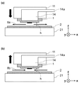
本発明の第1実施形態のインプリント装置100について、図1を参照して説明する。インプリント装置は、半導体デバイスなどの製造に使用され、パターンが形成されたモールドを基板上の樹脂(インプリント材)と接触させた状態(押し付けた状態で樹脂を硬化させ、硬化した樹脂からモールドを剥離することで基板上にパターンを転写するインプリント処理を行う。インプリント装置100は、モールド1を保持するモールド保持部10と、基板2を保持する基板保持部20と、モールド1を変形させる変形部15と、基板上の樹脂に光(紫外光を照射する光照射部30と、基板2に樹脂を塗布する塗布部40とを含む。また、インプリント装置100は、インプリント処理を制御するための制御系50として、第1制御部51と、第2制御部52と、第3制御部53と、決定部54と、補正部55と、記憶部56とを含む。
<First Embodiment>
An imprint apparatus 100 according to a first embodiment of the present invention will be described with reference to FIG. The imprint apparatus is used in the manufacture of semiconductor devices and the like. From the cured resin, the resin is cured in a state ( pressed state ) in which the pattern-formed mold is in contact with the resin (imprint material) on the substrate. An imprint process for transferring the pattern onto the substrate is performed by peeling the mold. The imprint apparatus 100 irradiates the resin on the substrate with light ( ultraviolet light ) , the mold holding unit 10 that holds the mold 1, the substrate holding unit 20 that holds the substrate 2, the deformation unit 15 that deforms the mold 1. The light irradiation part 30 to perform and the application part 40 which apply | coats resin to the board | substrate 2 are included. The imprint apparatus 100 also includes a first control unit 51, a second control unit 52, a third control unit 53, a determination unit 54, and a correction unit 55 as a control system 50 for controlling the imprint process. And a storage unit 56.

モールド1は、通常、石英など紫外線を透過させることができる材料で作製されており、基板側の面の一部には、基板上の樹脂に転写する凹凸のパターン1aが形成されている。また、モールド1の基板側の面と反対側の面には、パターン1aが形成された部分の厚みが薄くなるように掘り込まれた凹部1bが形成されている。このように、パターン1aが形成された部分を薄くすることで、後述する気室14に圧力を加えたときにモールド1が変形しやすい状態にしている。基板2は、例えば、単結晶シリコン基板やSOI(Silicon on Insulator)基板が用いられる。基板2の上面(被処理面)には、後述する塗布部40によって紫外線硬化樹脂(以下、樹脂)が塗布され、基板2に塗布された樹脂にモールド1が押し付けられる。樹脂にモールド1が押し付けられた状態で紫外線31aを照射することによって樹脂が硬化し、硬化した樹脂からモールド1が剥離されることによって樹脂にモールド1のパターン1aが転写される。 The mold 1 is usually made of a material that can transmit ultraviolet rays, such as quartz, and an uneven pattern 1a to be transferred to a resin on the substrate is formed on a part of the surface on the substrate side. A recess 1b is formed on the surface of the mold 1 opposite to the surface on the substrate side so as to reduce the thickness of the portion where the pattern 1a is formed. Thus, by thinning the portion where the pattern 1a is formed, the mold 1 is easily deformed when pressure is applied to an air chamber 14 described later. As the substrate 2, for example, a single crystal silicon substrate or an SOI (Silicon on Insulator) substrate is used. An ultraviolet curable resin (hereinafter, resin) is applied to the upper surface (surface to be processed ) of the substrate 2 by an application unit 40 described later, and the mold 1 is pressed against the resin applied to the substrate 2. When the mold 1 is pressed against the resin, the resin is cured by irradiating the ultraviolet rays 31a, and the mold 1 is peeled off from the cured resin, whereby the pattern 1a of the mold 1 is transferred to the resin.

モールド保持部10は、モールドチャック11と、位置計測部12とを含む。モールドチャック11は、z方向に推力を発生させるアクチュエータ13を介して構造体3に固定されており、真空吸着力や静電力などによりモールド1を保持する。モールドチャック11にはモールド1と接触する面に凹部11aが形成されており、モールドチャック11の凹部11aは、モールド1により覆われてほぼ密閉された空間となる。モールドチャック11の凹部11aとモールド1の凹部1bとによって規定される空間を、以下では気室14と呼ぶ。気室14は、配管14aを介して変形部15に接続されている。変形部15は、気室14に圧縮空気を供給する供給源と気室14を真空にする排気装置とを切り替えるための切換え弁やサーボバルブなどの圧力調整器15a(図4)を含む。この変形部15によってインプリント処理時に気室14の圧力を制御し、モールド1を基板2に向かって凸型の形状に変形させることができる。このように、モールド1を変形させてインプリント処理を行うと、モールド1はその中心部から基板2に接触していくため、モールド1のパターン1aに気泡が閉じ込められることが抑制され、基板上に転写されるパターンの欠損を防止することができる。アクチュエータ13は、例えば、3個以上用いることによって、モールドチャック11(モールド1)の位置および姿勢をz方向、x軸まわりの回転(θ)、およびy軸まわりの回転(θ)について制御することができる。また、位置計測部12は、例えば、エンコーダや干渉計、静電容量センサなどを含み、モールドチャック11の位置を計測する。位置計測部12は、例えば、3個以上のエンコーダを含む場合、モールドチャック11におけるz方向の位置、x軸を中心にしたθ回転量、およびy軸を中心にしたθ回転量を計測することができる。ここで、モールド保持部10が固定される構造体3は、インプリント装置が固定された場所(床)からの振動を抑制するため、床に固定された定盤6によって、支持台5および空気ばね4を介して支持されている。また、構造体3を支持台5および定盤6と一体化し、定盤6の下に空気ばね4を挿入する構成にしてもよく、この場合も床からの振動を抑制できる。また、第1実施形態において変形部15は、気室14の圧力を調整してモールド1を変形しているが、例えば、圧電素子などによってモールド1の側面から力を加えてモールド1を変形してもよい。 The mold holding unit 10 includes a mold chuck 11 and a position measurement unit 12. The mold chuck 11 is fixed to the structure 3 via an actuator 13 that generates a thrust force in the z direction, and holds the mold 1 by a vacuum suction force or an electrostatic force. The mold chuck 11 has a recess 11 a formed on the surface that contacts the mold 1. The recess 11 a of the mold chuck 11 is covered with the mold 1 and becomes a substantially sealed space. A space defined by the concave portion 11a of the mold chuck 11 and the concave portion 1b of the mold 1 is hereinafter referred to as an air chamber 14. The air chamber 14 is connected to the deformation part 15 via the pipe 14a. The deformation unit 15 includes a pressure regulator 15a (FIG. 4) such as a switching valve or a servo valve for switching between a supply source for supplying compressed air to the air chamber 14 and an exhaust device for evacuating the air chamber 14. By this deforming portion 15, the pressure of the air chamber 14 can be controlled during the imprint process, and the mold 1 can be deformed into a convex shape toward the substrate 2. When the imprint process is performed by deforming the mold 1 in this manner, the mold 1 comes into contact with the substrate 2 from the central portion thereof, so that air bubbles are suppressed from being confined in the pattern 1a of the mold 1, and It is possible to prevent the loss of the pattern transferred to the surface. For example, by using three or more actuators 13, the position and posture of the mold chuck 11 (mold 1) are controlled with respect to the z direction, rotation about the x axis (θ x ), and rotation about the y axis (θ y ). can do. The position measurement unit 12 includes, for example, an encoder, an interferometer, a capacitance sensor, and the like, and measures the position of the mold chuck 11. For example, when the position measurement unit 12 includes three or more encoders, the position measurement unit 12 measures the position in the z direction of the mold chuck 11, the θ x rotation amount around the x axis, and the θ y rotation amount around the y axis. can do. Here, the structure 3 to which the mold holding unit 10 is fixed has the support base 5 and the air by the surface plate 6 fixed to the floor in order to suppress vibration from the place (floor) where the imprint apparatus is fixed. It is supported via a spring 4. Further, the structure 3 may be integrated with the support base 5 and the surface plate 6 and the air spring 4 may be inserted under the surface plate 6. In this case, vibration from the floor can be suppressed. Further, in the first embodiment, the deforming portion 15 deforms the mold 1 by adjusting the pressure of the air chamber 14. For example, the deforming portion 15 deforms the mold 1 by applying a force from the side surface of the mold 1 with a piezoelectric element or the like. May be.

基板保持部20は、基板チャック21と、ステージ駆動部22と、位置計測部23とを含む。基板チャック21は、z方向に推力を発生させるアクチュエータ24を介してステージ駆動部22に固定されており、真空吸着力や静電力などにより基板2を保持する。アクチュエータ24は、例えば、3個以上用いることによって、基板チャック21(基板2)の位置および姿勢をz方向、x軸まわりの回転(θ)、およびy軸まわりの回転(θ)について制御することができる。ステージ駆動部22は、例えば、リニアモーターを含み、基板チャック21をx方向およびy方向に移動可能にする。また、位置計測部23は、例えば、エンコーダや干渉計、静電容量センサなどを含み、基板チャック21の位置を計測する。位置計測部23は、例えば、干渉計を含む場合、基板チャック21におけるx方向、y方向およびz方向の位置、並びにθ回転量、θ回転量およびθ回転量(z軸まわりの回転量)を計測することができる。 The substrate holding unit 20 includes a substrate chuck 21, a stage drive unit 22, and a position measurement unit 23. The substrate chuck 21 is fixed to the stage drive unit 22 via an actuator 24 that generates a thrust in the z direction, and holds the substrate 2 by a vacuum suction force or an electrostatic force. For example, by using three or more actuators 24, the position and posture of the substrate chuck 21 (substrate 2) are controlled with respect to the z direction, rotation about the x axis (θ x ), and rotation about the y axis (θ y ). can do. The stage drive unit 22 includes, for example, a linear motor, and allows the substrate chuck 21 to move in the x direction and the y direction. The position measurement unit 23 includes, for example, an encoder, an interferometer, a capacitance sensor, and the like, and measures the position of the substrate chuck 21. For example, when the position measurement unit 23 includes an interferometer, the position of the substrate chuck 21 in the x direction, the y direction, and the z direction, the θ x rotation amount, the θ y rotation amount, and the θ z rotation amount (rotation around the z axis). Quantity) can be measured.

光照射部30は、光源31と光学素子32を含む。光源31は、基板2に塗布された樹脂を硬化させる紫外線31aを射出する。光学素子32は、光源31から射出された紫外線31aを折り曲げるミラーで構成され、インプリント処理の際にモールド1を介して基板上の樹脂に紫外線31aを照射する。第1実施形態のインプリント装置100では、パターン1aが形成されたモールド1を基板上の樹脂に接触させ、この状態で光源31からの紫外線31aを照射して樹脂を硬化させる。ここで、第1実施形態では、光硬化法を採用するため光照射部30が設置されているが、例えば、熱硬化法を採用する場合には、光照射部30の代わりに熱硬化性樹脂を硬化するための熱源部を設置してもよい。   The light irradiation unit 30 includes a light source 31 and an optical element 32. The light source 31 emits ultraviolet rays 31 a that cure the resin applied to the substrate 2. The optical element 32 includes a mirror that bends the ultraviolet rays 31a emitted from the light source 31, and irradiates the resin on the substrate with the ultraviolet rays 31a through the mold 1 during the imprint process. In the imprint apparatus 100 of the first embodiment, the mold 1 on which the pattern 1a is formed is brought into contact with the resin on the substrate, and in this state, the ultraviolet light 31a from the light source 31 is irradiated to cure the resin. Here, in 1st Embodiment, although the light irradiation part 30 is installed in order to employ | adopt a photocuring method, when employ | adopting a thermosetting method, for example, it is a thermosetting resin instead of the light irradiation part 30. You may install the heat-source part for hardening | curing.

塗布部40は、基板上に樹脂(未硬化樹脂)を塗布する。上述したように、第1実施形態で用いられる樹脂は、紫外線31aの照射によって硬化する性質を有する光硬化性樹脂(インプリント材)であり、半導体デバイス製造工程における各種条件によって適宜選択される。また、塗布部40の吐出ノズルから吐出される樹脂の量は、基板上の樹脂に形成される凹凸のパターンにおいて、そのパターンの厚さや、凹凸の密度などによって適宜決定される。ここで、基板上の樹脂は、モールド1を接触させた状態で一定の時間を経過させ、モールドのパターンの隅々まで充填される。このとき、モールド1と基板2との間に気泡が閉じ込められてしまうと、基板上に形成されたパターンに欠損が生じてしまう。例えば、空気中でインプリント処理を行う場合、空気は樹脂に溶けにくいため、モールド1と基板2との間に気泡が生じ易い。そのため、第1実施形態では、基板上の樹脂に溶けやすい不活性ガスを供給するガスノズル41が備えられている。   The application unit 40 applies a resin (uncured resin) on the substrate. As described above, the resin used in the first embodiment is a photo-curable resin (imprint material) having a property of being cured by irradiation with ultraviolet rays 31a, and is appropriately selected according to various conditions in the semiconductor device manufacturing process. In addition, the amount of resin discharged from the discharge nozzle of the application unit 40 is appropriately determined by the thickness of the pattern, the density of the unevenness, and the like in the uneven pattern formed on the resin on the substrate. Here, the resin on the substrate is filled up to every corner of the pattern of the mold after a predetermined time has passed while the mold 1 is in contact. At this time, if bubbles are confined between the mold 1 and the substrate 2, the pattern formed on the substrate will be deficient. For example, when the imprint process is performed in the air, since air is not easily dissolved in the resin, bubbles are easily generated between the mold 1 and the substrate 2. Therefore, in 1st Embodiment, the gas nozzle 41 which supplies the inert gas which is easy to melt | dissolve in resin on a board | substrate is provided.

第1制御部51は、インプリント処理を行う際において、モールド1の位置(z方向、θおよびθ)が目標位置になるようにモールド保持部10を制御する。第2制御部52は、インプリント処理を行う際において、基板2の位置(x方向、y方向、z方向、θ、θおよびθ)が目標位置になるように基板保持部20を制御する。第3制御部53は、インプリント処理を行う際において、モールド1の形状が目標形状になるように変形部15を制御する。 When performing the imprint process, the first control unit 51 controls the mold holding unit 10 so that the position of the mold 1 (z direction, θ x and θ y ) is a target position. When performing the imprint process, the second control unit 52 moves the substrate holding unit 20 so that the position of the substrate 2 (x direction, y direction, z direction, θ x , θ y, and θ z ) is a target position. Control. The third control unit 53 controls the deforming unit 15 so that the shape of the mold 1 becomes a target shape when performing the imprint process.

近年、半導体デバイスなどの製造では、複数のパターンを1つの基板上に重ね合わせる工程が必要であるほか、回路パターンの微細化も進んでいる。そのため、第1実施形態のインプリント装置100において、パターンが形成されるべき基板上の領域にモールド1のパターン1aを高精度に転写することが重要である。即ち、モールド1と基板2とを高精度にアライメントすることが重要である。ここで、第1実施形態のインプリント装置100におけるアライメントについて説明する。インプリント装置100におけるアライメント方法としては、グローバルアライメント方式とダイバイダイアライメント方式とがある。グローバルアライメント方式は、基板上の数箇所のショット領域(サンプルショット領域)に形成されたマークの検出結果を統計処理して得られる指標に従ってアライメントを行う方式である。即ち、グローバルアライメント方式では、全てのショット領域に対して同一の指標でアライメントが行われる。一方で、ダイバイダイアライメント方式は、基板上の複数のショット領域ごとに、各ショット領域に形成されたマークの検出結果に従ってアライメントを行う方式である。このようなアライメントは、インプリント処理において樹脂を硬化させる前に行われ、モールド1のパターン1aを基板2に転写する上で重要な工程である。しかしながら、インプリント処理においてモールド1と基板2との距離を変更する際、それらの間における気体の流れに起因して、それらの距離を変更することを妨げる抗力が生じてしまう。このような抗力は、モールド1と基板2との相対位置を制御するときの外乱となる。そのため、モールド1と基板2との距離を変更する際に、それらが傾いた状態で接触したり、それらの相対位置が基板面と平行な方向にずれたりしうる。その結果、モールド1と基板2とを高精度にアライメントすることが困難となり、基板上に形成されたパターンにおいて位置ずれや欠損が発生しうる。抗力を抑制する1つの手段として、モールド1と基板2との相対速度を低下させることが挙げられる。しかし、それらの相対速度を低下させることは、インプリント装置のスループットを低下させてしまうこととなる。そこで、第1実施形態のインプリント装置100は、決定部54と補正部55とを備えており、第1制御部51、第2制御部52および第3制御部53に対してフィードフォワード制御を行う。   In recent years, in the manufacture of semiconductor devices and the like, a process of superimposing a plurality of patterns on a single substrate is required, and circuit patterns have been miniaturized. Therefore, in the imprint apparatus 100 according to the first embodiment, it is important to transfer the pattern 1a of the mold 1 with high accuracy to the region on the substrate where the pattern is to be formed. That is, it is important to align the mold 1 and the substrate 2 with high accuracy. Here, alignment in the imprint apparatus 100 of the first embodiment will be described. As an alignment method in the imprint apparatus 100, there are a global alignment method and a die-by-die alignment method. The global alignment method is a method of performing alignment according to an index obtained by statistically processing the detection results of marks formed in several shot regions (sample shot regions) on a substrate. That is, in the global alignment method, alignment is performed with the same index for all shot regions. On the other hand, the die-by-die alignment method is a method in which alignment is performed for each of a plurality of shot regions on the substrate according to the detection result of the mark formed in each shot region. Such alignment is performed before the resin is cured in the imprint process, and is an important process for transferring the pattern 1 a of the mold 1 to the substrate 2. However, when the distance between the mold 1 and the substrate 2 is changed in the imprint process, a drag that prevents the distance from being changed occurs due to the gas flow between them. Such a drag becomes a disturbance when the relative position between the mold 1 and the substrate 2 is controlled. For this reason, when the distance between the mold 1 and the substrate 2 is changed, they can come into contact with each other in an inclined state, or their relative positions can be shifted in a direction parallel to the substrate surface. As a result, it is difficult to align the mold 1 and the substrate 2 with high accuracy, and a positional deviation or a defect may occur in the pattern formed on the substrate. One means for suppressing the drag is to reduce the relative speed between the mold 1 and the substrate 2. However, reducing the relative speed of these will reduce the throughput of the imprint apparatus. Therefore, the imprint apparatus 100 according to the first embodiment includes a determination unit 54 and a correction unit 55, and performs feedforward control on the first control unit 51, the second control unit 52, and the third control unit 53. Do.

決定部54は、モールド1と基板2との距離に基づいて抗力を決定する。ここで、モールド1と基板2との距離を変更するときの抗力について図2を参照して説明する。図2(a)は、モールド1と基板2とを近づけることによって、モールド1と基板2との間における気体が外部に押し出される様子を示す。図2(a)において矢印8aは、気体の流れを示す。モールド1と基板2とを近づけていくと、それらの間における気体が中心から外側に向かって押し出される。このとき、気体はそれぞれ固有の粘性係数を有する(例えば、20℃の空気の粘性係数は1.8×10⁻⁵/Pa・sec)ため、モールド1と基板2とを近づけることを妨げる抗力が生じる。同様に、図2(b)は、モールド1と基板2とを離すことによって、モールド1と基板2との間に気体が流入する様子を示す。図2(b)において矢印8bは、気体の流れを示す。モールド1と基板2とを離していくと、それらの間における気体が外側から中心に向かって流入する。このときも、気体の粘性係数によって、モールド1と基板2とを離すことを妨げる抗力が生じる。このような抗力は、モールド1と基板2との距離の3乗に反比例し、モールド1と基板2との相対速度に比例するため、抗力をF、距離をh、相対速度をdh/dtおよび係数をKとすると式(1)によって表される。 The determination unit 54 determines the drag based on the distance between the mold 1 and the substrate 2. Here, the drag when changing the distance between the mold 1 and the substrate 2 will be described with reference to FIG. FIG. 2A shows how the gas between the mold 1 and the substrate 2 is pushed out by bringing the mold 1 and the substrate 2 close to each other. In FIG. 2A, an arrow 8a indicates a gas flow. When the mold 1 and the substrate 2 are brought closer to each other, the gas between them is pushed outward from the center. At this time, since each gas has a specific viscosity coefficient (for example, the viscosity coefficient of air at 20 ° C. is 1.8 × 10 −5 / Pa · sec), the drag that prevents the mold 1 and the substrate 2 from approaching each other has a drag. Arise. Similarly, FIG. 2B shows a state in which gas flows between the mold 1 and the substrate 2 by separating the mold 1 and the substrate 2. In FIG. 2B, an arrow 8b indicates a gas flow. When the mold 1 and the substrate 2 are separated, the gas between them flows from the outside toward the center. Also at this time, a drag that prevents the mold 1 and the substrate 2 from being separated occurs due to the viscosity coefficient of the gas. Such a drag is inversely proportional to the cube of the distance between the mold 1 and the substrate 2 and proportional to the relative speed between the mold 1 and the substrate 2, so that the drag is F, the distance is h, the relative speed is dh / dt, and If the coefficient is K, it is expressed by equation (1).

Figure 0006166516
Figure 0006166516

係数Kは、モールド1と基板2との間における気体の粘性係数や、モールド1と基板2とが重なり合う面積によって決定される。例えば、20℃の空気中において、150mm角のモールド1が全面で基板2と重なり合う場合、係数Kは4×10⁻⁹N/sec・mとなる。 The coefficient K is determined by the viscosity coefficient of the gas between the mold 1 and the substrate 2 and the area where the mold 1 and the substrate 2 overlap. For example, in the air at 20 ° C., when the 150 mm square mold 1 overlaps the substrate 2 on the entire surface, the coefficient K is 4 × 10 −9 N / sec · m 2 .

基板2に複数のショット領域を形成する場合、各ショット領域において、気体の粘性係数は変化しないが、モールド1と基板2とが重なり合う面積が異なる。例えば、基板2の中心部分にショット領域を形成する場合では、モールド1と基板2とが重なり合う面積は、モールドの面積にほぼ等しくなる。この場合、抗力はモールド1および基板2に均等に加わるため、それらが傾いたり、それらの相対位置が基板面と平行な方向にずれたりすることは少ない。それに対し、基板2の中心部分から離れた位置にショット領域2aを形成する場合では、図3に示すように、モールド1と基板2とが重なり合う部分の面積は図3の斜線部となり、基板2の中心部分のショット領域を形成する場合と比べて小さくなる。また、この場合、斜線部に加わる抗力は、モールド1における斜線部以外の部分に加わる抗力と比べて、基板の厚み分(数百μm程度)だけ大きくなる。このように斜線部とそれ以外の部分とで抗力が異なると、モールド1と基板2とにモーメント(θおよびθ)が生じてそれらが傾いたり、それらの相対位置が基板面と平行な方向(x方向およびy方向)にずれたりする。そのため、第1実施形態のインプリント装置100は、基板上の位置と、その位置における係数Kとの対応関係を表す情報を記憶する記憶部56を含む。そして、決定部54は、インプリント処理が行われる基板上の位置に対応した係数Kを、記憶部56に記憶された情報によって取得する。ここで、係数Kは、z方向の抗力に加えて、モールド1と基板2とをx方向およびy方向にずらす力や、θおよびθに回転させる力を決定するための係数を含んでもよい。 When a plurality of shot regions are formed on the substrate 2, the gas viscosity coefficient does not change in each shot region, but the areas where the mold 1 and the substrate 2 overlap are different. For example, when a shot region is formed in the central portion of the substrate 2, the area where the mold 1 and the substrate 2 overlap is almost equal to the area of the mold. In this case, since the drag force is equally applied to the mold 1 and the substrate 2, they are unlikely to be tilted or their relative positions are not shifted in a direction parallel to the substrate surface. On the other hand, when the shot region 2a is formed at a position away from the central portion of the substrate 2, as shown in FIG. 3, the area where the mold 1 and the substrate 2 overlap is the shaded portion in FIG. This is smaller than the case of forming a shot region in the central portion of. In this case, the drag applied to the hatched portion is larger than the drag applied to the portion other than the hatched portion of the mold 1 by the thickness of the substrate (about several hundred μm). If the drag force is different between the hatched portion and the other portions in this way, moments (θ x and θ y ) are generated between the mold 1 and the substrate 2 and they are inclined, or their relative positions are parallel to the substrate surface. Shift in the direction (x direction and y direction). Therefore, the imprint apparatus 100 according to the first embodiment includes a storage unit 56 that stores information representing a correspondence relationship between the position on the substrate and the coefficient K at the position. Then, the determination unit 54 acquires the coefficient K corresponding to the position on the substrate where the imprint process is performed, using information stored in the storage unit 56. Here, the coefficient K may include a coefficient for determining a force for shifting the mold 1 and the substrate 2 in the x direction and the y direction, and a force for rotating them in θ x and θ y , in addition to the drag in the z direction. Good.

補正部55は、第1制御部51におけるモールド保持部10を制御するための情報(操作情報)、第2制御部52における基板保持部20を制御するための情報(操作情報)、および第3制御部53における変形部15を制御するための情報(操作情報)を補正する。ここで、第1制御部51、第2制御部52および第3制御部53における操作情報の補正について図4を参照して説明する。図4は、第1実施形態の制御系50を示すブロック図である。決定部54は、減算器54aと計算器54bとを含む。減算器54aは、位置計測部12によって計測されたモールドチャック11の位置と、位置計測部23によって計測された基板チャック21の位置との差分を算出し、算出した差分を計算器54bに供給する。計算器54bは、減算器54aから供給された差分によってモールド1と基板2との距離、およびそれらの距離を時間微分した相対速度を算出し、モールド1と基板2との距離を変更することを妨げる抗力を上述した式(1)に基づいて決定する。このとき、計算部54bは、z方向の抗力に基づいて、モールド1と基板2とをx方向およびy方向にずらす力や、それらをθおよびθに回転させる力を決定してもよい。補正部55は、決定部54によって決定された抗力によって、各制御部(51、52および53)を補正するための補正情報を生成する。このとき、例えば、基板2の中心部分にショット領域を形成する場合、上述したように、モールド1と基板2との相対位置が基板面と平行な方向にずれることは少ないため、補正部55は、z方向の抗力を補正するための補正情報を生成すれば足りる。一方で、図3に示すように、基板2の中心部分から離れた位置にショット領域2aを形成する場合、モールド1と基板2とをx方向およびy方向にずらす力や、それらをθおよびθに回転させる力が生じる。そのため、補正部55は、z方向の抗力を補正するための補正情報だけでなく、x方向およびy方向の力を補正するための補正情報、並びにθおよびθに回転させる力を補正するための補正情報を生成してもよい。このような補正情報は、各制御部における制御器(51b、52bおよび53b)の後に備えられた加算器(51c、52cおよび53c)によって、各制御器で生成された操作情報に加算される。ここで、第1実施形態の補正部55は、第1制御部51および第2制御部52の両方を補正しているが、それらのうち一方のみを補正してもよい。 The correction unit 55 is information (operation information) for controlling the mold holding unit 10 in the first control unit 51, information (operation information) for controlling the substrate holding unit 20 in the second control unit 52, and third. Information (operation information) for controlling the deformation unit 15 in the control unit 53 is corrected. Here, correction of operation information in the first control unit 51, the second control unit 52, and the third control unit 53 will be described with reference to FIG. FIG. 4 is a block diagram showing the control system 50 of the first embodiment. The determination unit 54 includes a subtractor 54a and a calculator 54b. The subtractor 54a calculates a difference between the position of the mold chuck 11 measured by the position measuring unit 12 and the position of the substrate chuck 21 measured by the position measuring unit 23, and supplies the calculated difference to the calculator 54b. . The calculator 54b calculates the distance between the mold 1 and the substrate 2 and the relative speed obtained by differentiating the distance with respect to the difference supplied from the subtractor 54a, and changes the distance between the mold 1 and the substrate 2. The drag force to be prevented is determined based on the above formula (1). At this time, the calculation unit 54b may determine a force for shifting the mold 1 and the substrate 2 in the x direction and the y direction and a force for rotating them in θ x and θ y based on the drag force in the z direction. . The correction unit 55 generates correction information for correcting each control unit (51, 52, and 53) based on the drag determined by the determination unit 54. At this time, for example, when the shot region is formed in the central portion of the substrate 2, as described above, the relative position between the mold 1 and the substrate 2 is unlikely to shift in a direction parallel to the substrate surface. It is sufficient to generate correction information for correcting the drag in the z direction. On the other hand, as shown in FIG. 3, when forming a shot area 2a to a position away from the center portion of the substrate 2, and a force to shift the mold 1 and the substrate 2 in the x and y directions, they theta x and A rotating force is generated in θ y . Therefore, the correction unit 55 corrects not only the correction information for correcting the drag force in the z direction, but also the correction information for correcting the force in the x direction and the y direction, and the force that rotates in θ x and θ y. Correction information may be generated. Such correction information is added to the operation information generated by each controller by an adder (51c, 52c and 53c) provided after the controller (51b, 52b and 53b) in each controller. Here, although the correction | amendment part 55 of 1st Embodiment correct | amends both the 1st control part 51 and the 2nd control part 52, you may correct | amend only one of them.

第1制御部51は、減算器51a、制御器51b、加算器51cおよび分配器51dを含む。減算器51aは、位置計測部12によって計測されたモールドチャック11の現在位置と目標位置との制御偏差を算出し、算出された制御偏差を制御器51bに供給する。制御器51bは、例えばPIDやローパスフィルタ、ノッチフィルタなどを含み、アクチュエータ13を駆動するための操作情報を生成する。加算器51cは、制御器51bで生成された操作情報に、補正部55から供給される補正情報を加算する。分配器51dは、各アクチュエータ13において必要な推力を補正された操作情報に基づいて計算し、その推力に対応した操作量(電圧)を各アクチュエータ13のドライバに供給する。これにより、各アクチュエータ13が駆動し、モールドチャック11を目標位置および目標姿勢に近づけることができる。同様に、第2制御部52は、減算器52a、制御器52b、加算器52cおよび分配器52dを含む。減算器52aは、位置計測部23によって計測された基板チャック21の現在位置と目標位置との制御偏差を算出し、算出された制御偏差を制御器52bに供給する。制御器52bは、例えばPIDやローパスフィルタ、ノッチフィルタなどを含み、アクチュエータ24を駆動するための操作情報を生成する。加算器52cは、制御器52bで生成された操作情報に、補正部55から供給された補正情報を加算する。分配器52dは、各アクチュエータ24において必要な推力を補正された操作情報に基づいて計算し、その推力に対応した操作量(電圧)を各アクチュエータ24のドライバに供給する。これにより、各アクチュエータ24が駆動し、基板チャック21を目標位置および目標姿勢に近づけることができる。   The first control unit 51 includes a subtractor 51a, a controller 51b, an adder 51c, and a distributor 51d. The subtractor 51a calculates a control deviation between the current position and the target position of the mold chuck 11 measured by the position measuring unit 12, and supplies the calculated control deviation to the controller 51b. The controller 51b includes, for example, a PID, a low-pass filter, a notch filter, and the like, and generates operation information for driving the actuator 13. The adder 51c adds the correction information supplied from the correction unit 55 to the operation information generated by the controller 51b. The distributor 51d calculates the thrust necessary for each actuator 13 based on the corrected operation information, and supplies an operation amount (voltage) corresponding to the thrust to the driver of each actuator 13. Thereby, each actuator 13 drives and the mold chuck 11 can be brought close to the target position and the target posture. Similarly, the second control unit 52 includes a subtractor 52a, a controller 52b, an adder 52c, and a distributor 52d. The subtractor 52a calculates a control deviation between the current position and the target position of the substrate chuck 21 measured by the position measurement unit 23, and supplies the calculated control deviation to the controller 52b. The controller 52b includes, for example, a PID, a low-pass filter, a notch filter, and the like, and generates operation information for driving the actuator 24. The adder 52c adds the correction information supplied from the correction unit 55 to the operation information generated by the controller 52b. The distributor 52d calculates the thrust necessary for each actuator 24 based on the corrected operation information, and supplies an operation amount (voltage) corresponding to the thrust to the driver of each actuator 24. Accordingly, each actuator 24 is driven, and the substrate chuck 21 can be brought close to the target position and the target posture.

第3制御部53は、減算器53a、制御器53b、加算器53cおよび駆動器53dを含む。減算器53aは、変形部15に含まれる圧力計測器15bによって計測された気室14の圧力値と目標値との制御偏差を算出し、算出された制御偏差を制御器53bに供給する。制御器53bは、例えばPIDやローパスフィルタ、ノッチフィルタなどを含み、変形部15における圧力調整器15aを駆動するための操作情報を生成する。加算器53cは、制御器53bで生成された操作情報に、補正部55から供給された補正情報を加算する。駆動器53dは、補正された操作情報に基づいて圧力調整器15aを駆動する。例えば、モールド1と基板2とを近づける場合、抗力は、モールド1が基板2に向かって凸型の形状に変形することを妨げるような抗力となる。この場合、補正部55は、モールド1と基板2との距離に基づいて、気室14の圧力を増やすように操作情報を補正するための補正情報を生成する。この補正情報は、加算器53cによって操作情報に加算される。そして、駆動器53dにおいて、補正された操作情報に基づいて圧力調整器15aが駆動される。これにより、モールド1と基板2との距離を変更する際の抗力が生じても、モールド1の変形量をほぼ一定にすることができる。ここで、第3制御部53における制御偏差は、圧力計測器15bで計測された気室14の圧力値とその目標値との差分であるが、モールド1の変形量を変位センサなどによって直接計測できる場合には、モールド1の変形量とその目標値との差分であってもよい。   The third control unit 53 includes a subtractor 53a, a controller 53b, an adder 53c, and a driver 53d. The subtractor 53a calculates a control deviation between the pressure value of the air chamber 14 measured by the pressure measuring instrument 15b included in the deforming unit 15 and the target value, and supplies the calculated control deviation to the controller 53b. The controller 53b includes, for example, a PID, a low-pass filter, a notch filter, and the like, and generates operation information for driving the pressure regulator 15a in the deformation unit 15. The adder 53c adds the correction information supplied from the correction unit 55 to the operation information generated by the controller 53b. The driver 53d drives the pressure regulator 15a based on the corrected operation information. For example, when the mold 1 and the substrate 2 are brought close to each other, the drag is a drag that prevents the mold 1 from being deformed into a convex shape toward the substrate 2. In this case, the correction unit 55 generates correction information for correcting the operation information so as to increase the pressure of the air chamber 14 based on the distance between the mold 1 and the substrate 2. This correction information is added to the operation information by the adder 53c. Then, in the driver 53d, the pressure regulator 15a is driven based on the corrected operation information. Thereby, even if the drag at the time of changing the distance of the mold 1 and the board | substrate 2 arises, the deformation amount of the mold 1 can be made substantially constant. Here, the control deviation in the third control unit 53 is a difference between the pressure value of the air chamber 14 measured by the pressure measuring instrument 15b and the target value, but the deformation amount of the mold 1 is directly measured by a displacement sensor or the like. If possible, it may be the difference between the deformation amount of the mold 1 and its target value.

上述したように、第1実施形態のインプリント装置100は、モールド1と基板2との距離に基づいて抗力を決定する決定部54と、各制御部(51、52および53)における操作情報を抗力に基づいて補正する補正部55とを含む。そして、決定部54および補正部55が各制御部(51、52および53)に対してフィードフォワード制御を行う。これにより、各制御部は、外乱として働く抗力を考慮してモールド保持部10、基板保持部20および変形部15を制御することができるため、モールド1と基板2とを高精度にアライメントすることができる。   As described above, the imprint apparatus 100 according to the first embodiment receives the operation information in the determination unit 54 that determines the drag based on the distance between the mold 1 and the substrate 2 and the control units (51, 52, and 53). And a correction unit 55 that corrects based on the drag. And the determination part 54 and the correction | amendment part 55 perform feedforward control with respect to each control part (51,52,53). Thereby, since each control part can control the mold holding part 10, the board | substrate holding part 20, and the deformation | transformation part 15 in consideration of the drag which acts as a disturbance, aligning the mold 1 and the board | substrate 2 with high precision. Can do.

<物品の製造方法の実施形態>
本発明の実施形態にかける物品の製造方法は、例えば、半導体デバイス等のマイクロデバイスや微細構造を有する素子等の物品を製造するのに好適である。本実施形態の物品の製造方法は、基板に塗布された樹脂に上記のインプリント装置を用いてパターンを形成する工程(基板にインプリント処理を行う工程)と、かかる工程でパターンが形成された基板を加工する工程とを含む。更に、かかる製造方法は、他の周知の工程(酸化、成膜、蒸着、ドーピング、平坦化、エッチング、レジスト剥離、ダイシング、ボンディング、パッケージング等)を含む。本実施形態の物品の製造方法は、従来の方法に比べて、物品の性能・品質・生産性・生産コストの少なくとも1つにおいて有利である。
<Embodiment of Method for Manufacturing Article>
The method for manufacturing an article according to an embodiment of the present invention is suitable for manufacturing an article such as a microdevice such as a semiconductor device or an element having a fine structure. In the method for manufacturing an article according to the present embodiment, a pattern is formed in a step of forming a pattern on the resin applied to the substrate using the above-described imprint apparatus (step of performing imprint processing on the substrate). Processing the substrate. Further, the manufacturing method includes other well-known steps (oxidation, film formation, vapor deposition, doping, planarization, etching, resist stripping, dicing, bonding, packaging, and the like). The method for manufacturing an article according to the present embodiment is advantageous in at least one of the performance, quality, productivity, and production cost of the article as compared with the conventional method.

以上、本発明の好ましい実施形態について説明したが、本発明はこれらの実施形態に限定されないことはいうまでもなく、その要旨の範囲内で種々の変形および変更が可能である。   As mentioned above, although preferred embodiment of this invention was described, it cannot be overemphasized that this invention is not limited to these embodiment, A various deformation | transformation and change are possible within the range of the summary.

Claims (7)

モールドを用いて基板上にインプリント材のパターンを形成するインプリント装置であって、
前記モールドを保持して移動可能なモールド保持部と、
前記基板を保持して移動可能な基板保持部と、
前記モールド保持部および前記基板保持部の移動を制御する制御部と、
前記モールドと前記基板との距離をh、前記モールドと前記基板との距離を変更するときの前記モールドと前記基板との相対速度をdh/dt、前記モールドと前記基板との間における気体の粘性係数および前記モールドと前記基板とが重なり合う面積によって決まる係数をKとするとき、前記モールドと前記基板との距離を変更するときの抗力Fを、
Figure 0006166516
に従って決定する決定部と、を有し、
前記制御部は、前記決定部で求められた抗力に基づいて前記モールド保持部および前記基板保持部の少なくとも一方の移動を制御することにより、前記モールドと前記基板との相対位置を変更することを特徴とするインプリント装置。
An imprint apparatus for forming a pattern of an imprint material on a substrate using a mold,
A mold holding unit that is movable while holding the mold;
A substrate holding part that is movable while holding the substrate;
A control unit for controlling movement of the mold holding unit and the substrate holding unit;
The distance between the mold and the substrate is h, the relative speed between the mold and the substrate when changing the distance between the mold and the substrate is dh / dt, and the viscosity of the gas between the mold and the substrate is When the coefficient and the coefficient determined by the area where the mold and the substrate overlap are K, the drag F when changing the distance between the mold and the substrate is
Figure 0006166516
Anda determination unit for determining in accordance with,
The control unit changes a relative position between the mold and the substrate by controlling movement of at least one of the mold holding unit and the substrate holding unit based on a drag obtained by the determination unit. A characteristic imprint apparatus.
モールドを用いて基板上にインプリント材のパターンを形成するインプリント処理を行うインプリント装置であって、
前記モールドを保持して移動可能なモールド保持部と、
前記基板を保持して移動可能な基板保持部と、
前記モールド保持部および前記基板保持部の移動を制御する制御部と、
前記モールドと前記基板との距離をh、前記モールドと前記基板との距離を変更するときの前記モールドと前記基板との相対速度をdh/dt、係数をKとするとき、前記モールドと前記基板との距離を変更するときの抗力Fを、
Figure 0006166516
に従って決定する決定部と、
前記基板上の位置と当該位置における前記係数との対応関係を表す情報を記憶する記憶部と、を有し、
前記制御部は、前記決定部で求められた抗力に基づいて前記モールド保持部および前記基板保持部の少なくとも一方の移動を制御することにより、前記モールドと前記基板との相対位置を変更し、
前記決定部は、前記インプリント処理が行われる前記基板上の位置に対応した前記係数を前記記憶部に記憶された前記情報から取得することを特徴とするインプリント装置。
An imprint apparatus that performs an imprint process for forming a pattern of an imprint material on a substrate using a mold,
A mold holding unit that is movable while holding the mold;
A substrate holding part that is movable while holding the substrate;
A control unit for controlling movement of the mold holding unit and the substrate holding unit;
When the distance between the mold and the substrate is h, the relative speed between the mold and the substrate when changing the distance between the mold and the substrate is dh / dt, and the coefficient is K, the mold and the substrate Drag F when changing the distance between
Figure 0006166516
A determination unit to determine according to
A storage unit for storing information representing a correspondence relationship between the position on the substrate and the coefficient at the position;
The control unit changes the relative position between the mold and the substrate by controlling the movement of at least one of the mold holding unit and the substrate holding unit based on the drag obtained by the determination unit ,
The determination unit is configured in the coefficient corresponding to the position on the substrate where the print processing is performed, the imprint apparatus and acquires from the information stored in the storage unit.
前記制御部は、前記モールドと前記インプリント材とが接触していない状態で前記距離を変更している際に生じる前記モールドと前記基板との相対位置のずれが補正されるように、前記決定部により求められた抗力に基づいて、前記モールド保持部および前記基板保持部の少なくとも一方を制御することを特徴とする請求項1又は2に記載のインプリント装置。 Wherein the control unit, as the deviation of the relative position between the mold and the substrate that occurs when said mold and said imprint material is changing the distance in a state not in contact is corrected, the decision 3. The imprint apparatus according to claim 1, wherein at least one of the mold holding unit and the substrate holding unit is controlled based on a drag obtained by the unit. 前記モールドと前記基板との相対位置のずれは、基板面と平行な方向における前記モールドと前記基板との相対位置のずれを含むことを特徴とする請求項に記載のインプリント装置。 The imprint apparatus according to claim 3 , wherein the displacement of the relative position between the mold and the substrate includes a displacement of the relative position between the mold and the substrate in a direction parallel to the substrate surface. 前記モールドに力を加えて前記パターンを変形させる変形部を更に含み、
前記制御部は、前記決定部により求められた抗力に基づいて前記変形部を制御することを特徴とする請求項1乃至4のうちいずれか1項に記載のインプリント装置。
And further including a deforming portion that deforms the pattern by applying a force to the mold,
Wherein the control unit, the imprint apparatus according to any one of claims 1 to 4, characterized in that to control the deformation portion on the basis of a drag that is determined by the determination unit.
請求項1乃至のうちいずれか1項に記載のインプリント装置を用いてパターンを前記基板に形成する形成工程と、
前記形成工程でパターンが形成された前記基板を加工する加工工程と、を有し
前記加工工程で加工された前記基板から物品を製造することを特徴とする物品の製造方法。
A forming step of forming a pattern on the substrate using the imprint apparatus according to any one of claims 1 to 5 ,
Anda processing step of processing the substrate on which the pattern is formed in the forming step,
A method for manufacturing an article, wherein the article is manufactured from the substrate processed in the processing step .
モールドを用いて基板上にインプリント材のパターンを形成するインプリント方法であって、
前記モールドと前記基板との距離をh、前記モールドと前記基板との距離を変更するときの前記モールドと前記基板との相対速度をdh/dt、前記モールドと前記基板との間における気体の粘性係数および前記モールドと前記基板とが重なり合う面積によって決まる係数をKとするとき、前記モールドと前記基板との距離を変更するときの抗力Fを、
Figure 0006166516
に従って決定する決定工程と、
前記決定工程で求められた抗力に基づいて、前記モールドと前記基板との相対位置を変更する変更工程と、
を有することを特徴とするインプリント方法。
An imprint method for forming a pattern of an imprint material on a substrate using a mold,
The distance between the mold and the substrate is h, the relative speed between the mold and the substrate when changing the distance between the mold and the substrate is dh / dt, and the viscosity of the gas between the mold and the substrate is When the coefficient and the coefficient determined by the area where the mold and the substrate overlap are K, the drag F when changing the distance between the mold and the substrate is
Figure 0006166516
A determination step to determine according to
Based on the drag determined in the determining step, a changing step for changing the relative position between the mold and the substrate;
The imprint method characterized by having .
JP2012159078A 2012-07-17 2012-07-17 Imprint apparatus, imprint method, and article manufacturing method Active JP6166516B2 (en)

Priority Applications (1)

Application Number Priority Date Filing Date Title
JP2012159078A JP6166516B2 (en) 2012-07-17 2012-07-17 Imprint apparatus, imprint method, and article manufacturing method

Applications Claiming Priority (1)

Application Number Priority Date Filing Date Title
JP2012159078A JP6166516B2 (en) 2012-07-17 2012-07-17 Imprint apparatus, imprint method, and article manufacturing method

Publications (3)

Publication Number Publication Date
JP2014022527A JP2014022527A (en) 2014-02-03
JP2014022527A5 JP2014022527A5 (en) 2015-09-03
JP6166516B2 true JP6166516B2 (en) 2017-07-19

Family

ID=50197089

Family Applications (1)

Application Number Title Priority Date Filing Date
JP2012159078A Active JP6166516B2 (en) 2012-07-17 2012-07-17 Imprint apparatus, imprint method, and article manufacturing method

Country Status (1)

Country Link
JP (1) JP6166516B2 (en)

Families Citing this family (3)

* Cited by examiner, † Cited by third party
Publication number Priority date Publication date Assignee Title
JP6562795B2 (en) * 2015-02-12 2019-08-21 キヤノン株式会社 Imprint apparatus and article manufacturing method
JP6700936B2 (en) 2016-04-25 2020-05-27 キヤノン株式会社 Imprint apparatus, imprint method, and article manufacturing method
JP7134055B2 (en) * 2018-10-09 2022-09-09 キヤノン株式会社 Molding apparatus and article manufacturing method

Family Cites Families (5)

* Cited by examiner, † Cited by third party
Publication number Priority date Publication date Assignee Title
JP2005101201A (en) * 2003-09-24 2005-04-14 Canon Inc Nano-imprint system
JP2007173614A (en) * 2005-12-22 2007-07-05 Ricoh Co Ltd Micro fabricating device
US9573319B2 (en) * 2007-02-06 2017-02-21 Canon Kabushiki Kaisha Imprinting method and process for producing a member in which a mold contacts a pattern forming layer
US8945444B2 (en) * 2007-12-04 2015-02-03 Canon Nanotechnologies, Inc. High throughput imprint based on contact line motion tracking control
JP5517423B2 (en) * 2008-08-26 2014-06-11 キヤノン株式会社 Imprint apparatus and imprint method

Also Published As

Publication number Publication date
JP2014022527A (en) 2014-02-03

Similar Documents

Publication Publication Date Title
JP6304934B2 (en) Imprint apparatus and article manufacturing method
KR102032095B1 (en) Method of curing uncured material and method of manufacturing article
JP6061524B2 (en) Imprint apparatus and article manufacturing method
KR101980415B1 (en) Imprint apparatus and article manufacturing method
US10216103B2 (en) Imprint method, imprint apparatus, and method of manufacturing article
US9823562B2 (en) Imprint apparatus, imprint method, and method of manufacturing article
KR20130059293A (en) Imprint apparatus, manufacturing method for article using the same, and imprint method
KR20130040723A (en) Imprint method, imprint apparatus and device manufacturing method
JP6029268B2 (en) Imprint apparatus and article manufacturing method using the same
US9971256B2 (en) Imprint apparatus, imprint method, and method of manufacturing article
US10216104B2 (en) Imprint method, imprint apparatus, and method of manufacturing article
JP6306830B2 (en) Imprint apparatus and article manufacturing method
JP6120677B2 (en) Imprint apparatus, imprint method, and article manufacturing method
KR101826393B1 (en) Imprint apparatus, imprint method, and method of manufacturing article
JP2016225433A (en) Mold, imprint method, imprint device, and method for producing article
JP2015050437A (en) Imprinting device and article manufacturing method
US20170008219A1 (en) Imprinting apparatus, imprinting method, and method of manufacturing object
JP2019204907A (en) Imprint device, imprint method and manufacturing method of article
JP6562795B2 (en) Imprint apparatus and article manufacturing method
JP6166516B2 (en) Imprint apparatus, imprint method, and article manufacturing method
JP7204457B2 (en) IMPRINT APPARATUS, IMPRINT METHOD, AND PRODUCT MANUFACTURING METHOD
JP2014175620A (en) Imprinting device, molding set, imprinting method, and article production method
JP2020188126A (en) Imprint apparatus, imprint method, and article manufacturing method
JP2018061061A (en) Imprint device, imprint method, and manufacturing method of article
JP2018060954A (en) Imprint device and method of manufacturing device

Legal Events

Date Code Title Description
A521 Written amendment

Free format text: JAPANESE INTERMEDIATE CODE: A523

Effective date: 20150715

A621 Written request for application examination

Free format text: JAPANESE INTERMEDIATE CODE: A621

Effective date: 20150715

A977 Report on retrieval

Free format text: JAPANESE INTERMEDIATE CODE: A971007

Effective date: 20160425

A131 Notification of reasons for refusal

Free format text: JAPANESE INTERMEDIATE CODE: A131

Effective date: 20160509

A521 Written amendment

Free format text: JAPANESE INTERMEDIATE CODE: A523

Effective date: 20160708

A131 Notification of reasons for refusal

Free format text: JAPANESE INTERMEDIATE CODE: A131

Effective date: 20161125

A521 Written amendment

Free format text: JAPANESE INTERMEDIATE CODE: A523

Effective date: 20170124

TRDD Decision of grant or rejection written
A01 Written decision to grant a patent or to grant a registration (utility model)

Free format text: JAPANESE INTERMEDIATE CODE: A01

Effective date: 20170526

A61 First payment of annual fees (during grant procedure)

Free format text: JAPANESE INTERMEDIATE CODE: A61

Effective date: 20170623

R151 Written notification of patent or utility model registration

Ref document number: 6166516

Country of ref document: JP

Free format text: JAPANESE INTERMEDIATE CODE: R151