JP6127869B2 - Solid-state imaging device, driving method thereof, and electronic apparatus - Google Patents
Solid-state imaging device, driving method thereof, and electronic apparatus Download PDFInfo
- Publication number
- JP6127869B2 JP6127869B2 JP2013197872A JP2013197872A JP6127869B2 JP 6127869 B2 JP6127869 B2 JP 6127869B2 JP 2013197872 A JP2013197872 A JP 2013197872A JP 2013197872 A JP2013197872 A JP 2013197872A JP 6127869 B2 JP6127869 B2 JP 6127869B2
- Authority
- JP
- Japan
- Prior art keywords
- photoelectric conversion
- conversion unit
- region
- unit
- pixel
- Prior art date
- Legal status (The legal status is an assumption and is not a legal conclusion. Google has not performed a legal analysis and makes no representation as to the accuracy of the status listed.)
- Active
Links
- 238000003384 imaging method Methods 0.000 title claims description 62
- 238000000034 method Methods 0.000 title claims description 31
- 238000006243 chemical reaction Methods 0.000 claims description 156
- 238000012546 transfer Methods 0.000 claims description 52
- 239000012535 impurity Substances 0.000 claims description 27
- 238000001514 detection method Methods 0.000 claims description 19
- 238000009825 accumulation Methods 0.000 claims description 17
- 239000011159 matrix material Substances 0.000 claims description 13
- 239000002184 metal Substances 0.000 claims description 5
- 238000000926 separation method Methods 0.000 claims description 4
- 238000012545 processing Methods 0.000 description 30
- 238000005516 engineering process Methods 0.000 description 21
- 238000012937 correction Methods 0.000 description 16
- 210000001747 pupil Anatomy 0.000 description 16
- 230000002093 peripheral effect Effects 0.000 description 14
- 230000000875 corresponding effect Effects 0.000 description 13
- 230000006870 function Effects 0.000 description 9
- 238000002955 isolation Methods 0.000 description 8
- 239000000758 substrate Substances 0.000 description 7
- 230000003321 amplification Effects 0.000 description 6
- 238000009792 diffusion process Methods 0.000 description 6
- 238000003199 nucleic acid amplification method Methods 0.000 description 6
- 239000004065 semiconductor Substances 0.000 description 6
- 238000010586 diagram Methods 0.000 description 5
- 230000003287 optical effect Effects 0.000 description 5
- 238000013500 data storage Methods 0.000 description 4
- 230000007423 decrease Effects 0.000 description 3
- 239000007787 solid Substances 0.000 description 2
- 238000004364 calculation method Methods 0.000 description 1
- 230000000295 complement effect Effects 0.000 description 1
- 230000001276 controlling effect Effects 0.000 description 1
- 230000002596 correlated effect Effects 0.000 description 1
- 238000005401 electroluminescence Methods 0.000 description 1
- 239000004973 liquid crystal related substance Substances 0.000 description 1
- 229910044991 metal oxide Inorganic materials 0.000 description 1
- 150000004706 metal oxides Chemical class 0.000 description 1
- 238000012986 modification Methods 0.000 description 1
- 230000004048 modification Effects 0.000 description 1
- 239000002245 particle Substances 0.000 description 1
- 230000011514 reflex Effects 0.000 description 1
- 238000005070 sampling Methods 0.000 description 1
- 230000001629 suppression Effects 0.000 description 1
Images


Classifications
-
- H—ELECTRICITY
- H01—ELECTRIC ELEMENTS
- H01L—SEMICONDUCTOR DEVICES NOT COVERED BY CLASS H10
- H01L27/00—Devices consisting of a plurality of semiconductor or other solid-state components formed in or on a common substrate
- H01L27/14—Devices consisting of a plurality of semiconductor or other solid-state components formed in or on a common substrate including semiconductor components sensitive to infrared radiation, light, electromagnetic radiation of shorter wavelength or corpuscular radiation and specially adapted either for the conversion of the energy of such radiation into electrical energy or for the control of electrical energy by such radiation
- H01L27/144—Devices controlled by radiation
- H01L27/146—Imager structures
-
- H—ELECTRICITY
- H04—ELECTRIC COMMUNICATION TECHNIQUE
- H04N—PICTORIAL COMMUNICATION, e.g. TELEVISION
- H04N25/00—Circuitry of solid-state image sensors [SSIS]; Control thereof
- H04N25/70—SSIS architectures; Circuits associated therewith
- H04N25/703—SSIS architectures incorporating pixels for producing signals other than image signals
- H04N25/704—Pixels specially adapted for focusing, e.g. phase difference pixel sets
-
- H—ELECTRICITY
- H01—ELECTRIC ELEMENTS
- H01L—SEMICONDUCTOR DEVICES NOT COVERED BY CLASS H10
- H01L27/00—Devices consisting of a plurality of semiconductor or other solid-state components formed in or on a common substrate
- H01L27/14—Devices consisting of a plurality of semiconductor or other solid-state components formed in or on a common substrate including semiconductor components sensitive to infrared radiation, light, electromagnetic radiation of shorter wavelength or corpuscular radiation and specially adapted either for the conversion of the energy of such radiation into electrical energy or for the control of electrical energy by such radiation
- H01L27/144—Devices controlled by radiation
- H01L27/146—Imager structures
- H01L27/14601—Structural or functional details thereof
- H01L27/14603—Special geometry or disposition of pixel-elements, address-lines or gate-electrodes
- H01L27/14605—Structural or functional details relating to the position of the pixel elements, e.g. smaller pixel elements in the center of the imager compared to pixel elements at the periphery
-
- H—ELECTRICITY
- H01—ELECTRIC ELEMENTS
- H01L—SEMICONDUCTOR DEVICES NOT COVERED BY CLASS H10
- H01L27/00—Devices consisting of a plurality of semiconductor or other solid-state components formed in or on a common substrate
- H01L27/14—Devices consisting of a plurality of semiconductor or other solid-state components formed in or on a common substrate including semiconductor components sensitive to infrared radiation, light, electromagnetic radiation of shorter wavelength or corpuscular radiation and specially adapted either for the conversion of the energy of such radiation into electrical energy or for the control of electrical energy by such radiation
- H01L27/144—Devices controlled by radiation
- H01L27/146—Imager structures
- H01L27/14601—Structural or functional details thereof
- H01L27/14609—Pixel-elements with integrated switching, control, storage or amplification elements
- H01L27/1461—Pixel-elements with integrated switching, control, storage or amplification elements characterised by the photosensitive area
-
- H—ELECTRICITY
- H01—ELECTRIC ELEMENTS
- H01L—SEMICONDUCTOR DEVICES NOT COVERED BY CLASS H10
- H01L27/00—Devices consisting of a plurality of semiconductor or other solid-state components formed in or on a common substrate
- H01L27/14—Devices consisting of a plurality of semiconductor or other solid-state components formed in or on a common substrate including semiconductor components sensitive to infrared radiation, light, electromagnetic radiation of shorter wavelength or corpuscular radiation and specially adapted either for the conversion of the energy of such radiation into electrical energy or for the control of electrical energy by such radiation
- H01L27/144—Devices controlled by radiation
- H01L27/146—Imager structures
- H01L27/14643—Photodiode arrays; MOS imagers
- H01L27/14645—Colour imagers
-
- H—ELECTRICITY
- H04—ELECTRIC COMMUNICATION TECHNIQUE
- H04N—PICTORIAL COMMUNICATION, e.g. TELEVISION
- H04N23/00—Cameras or camera modules comprising electronic image sensors; Control thereof
- H04N23/60—Control of cameras or camera modules
- H04N23/67—Focus control based on electronic image sensor signals
- H04N23/672—Focus control based on electronic image sensor signals based on the phase difference signals
-
- H—ELECTRICITY
- H04—ELECTRIC COMMUNICATION TECHNIQUE
- H04N—PICTORIAL COMMUNICATION, e.g. TELEVISION
- H04N25/00—Circuitry of solid-state image sensors [SSIS]; Control thereof
- H04N25/60—Noise processing, e.g. detecting, correcting, reducing or removing noise
-
- H—ELECTRICITY
- H04—ELECTRIC COMMUNICATION TECHNIQUE
- H04N—PICTORIAL COMMUNICATION, e.g. TELEVISION
- H04N25/00—Circuitry of solid-state image sensors [SSIS]; Control thereof
- H04N25/60—Noise processing, e.g. detecting, correcting, reducing or removing noise
- H04N25/616—Noise processing, e.g. detecting, correcting, reducing or removing noise involving a correlated sampling function, e.g. correlated double sampling [CDS] or triple sampling
-
- H—ELECTRICITY
- H04—ELECTRIC COMMUNICATION TECHNIQUE
- H04N—PICTORIAL COMMUNICATION, e.g. TELEVISION
- H04N25/00—Circuitry of solid-state image sensors [SSIS]; Control thereof
- H04N25/60—Noise processing, e.g. detecting, correcting, reducing or removing noise
- H04N25/67—Noise processing, e.g. detecting, correcting, reducing or removing noise applied to fixed-pattern noise, e.g. non-uniformity of response
- H04N25/671—Noise processing, e.g. detecting, correcting, reducing or removing noise applied to fixed-pattern noise, e.g. non-uniformity of response for non-uniformity detection or correction
-
- H—ELECTRICITY
- H04—ELECTRIC COMMUNICATION TECHNIQUE
- H04N—PICTORIAL COMMUNICATION, e.g. TELEVISION
- H04N25/00—Circuitry of solid-state image sensors [SSIS]; Control thereof
- H04N25/70—SSIS architectures; Circuits associated therewith
- H04N25/76—Addressed sensors, e.g. MOS or CMOS sensors
-
- H—ELECTRICITY
- H04—ELECTRIC COMMUNICATION TECHNIQUE
- H04N—PICTORIAL COMMUNICATION, e.g. TELEVISION
- H04N25/00—Circuitry of solid-state image sensors [SSIS]; Control thereof
- H04N25/10—Circuitry of solid-state image sensors [SSIS]; Control thereof for transforming different wavelengths into image signals
- H04N25/11—Arrangement of colour filter arrays [CFA]; Filter mosaics
- H04N25/13—Arrangement of colour filter arrays [CFA]; Filter mosaics characterised by the spectral characteristics of the filter elements
- H04N25/134—Arrangement of colour filter arrays [CFA]; Filter mosaics characterised by the spectral characteristics of the filter elements based on three different wavelength filter elements
Landscapes
- Engineering & Computer Science (AREA)
- Physics & Mathematics (AREA)
- Power Engineering (AREA)
- Multimedia (AREA)
- Signal Processing (AREA)
- General Physics & Mathematics (AREA)
- Condensed Matter Physics & Semiconductors (AREA)
- Electromagnetism (AREA)
- Computer Hardware Design (AREA)
- Microelectronics & Electronic Packaging (AREA)
- Solid State Image Pick-Up Elements (AREA)
- Transforming Light Signals Into Electric Signals (AREA)
- Color Television Image Signal Generators (AREA)
Description
本技術は、固体撮像素子及びその駆動方法、並びに電子機器に関し、特に、チップ位置によらず、位相差画素の特性を一定にすることができるようにした固体撮像素子及びその駆動方法、並びに電子機器に関する。 The present technology relates to a solid-state imaging device, a driving method thereof, and an electronic device, and in particular, a solid-state imaging device capable of making the characteristics of a phase difference pixel constant regardless of a chip position, a driving method thereof, and an electronic device Regarding equipment.
従来より、CMOS(Complementary Metal Oxide Semiconductor)イメージセンサなどの固体撮像素子は、撮像装置に広く用いられている。この種の撮像装置では、ピント合わせを自動化するAF(Autofocus)機能を備えているが、近年、被写体のAF精度やAF速度に対する要求はますます強くなっている。 Conventionally, solid-state imaging devices such as complementary metal oxide semiconductor (CMOS) image sensors have been widely used in imaging devices. This type of imaging apparatus has an AF (Autofocus) function that automates focusing, but in recent years, there has been an increasing demand for AF accuracy and AF speed of the subject.
例えば、デジタル一眼レフカメラでは一般的に、AFモジュールが追加で組み込まれているが、筐体サイズや実装コストの増大を伴うことになる。そのため、ミラーレス一眼カメラやコンパクトデジタルスチルカメラの中には、AFモジュールを別途組み込まず、コントラストAFによりAF機能を実現している機種があるが、現状ではAF速度が十分であるとは言い難い。 For example, a digital single-lens reflex camera generally includes an additional AF module, which increases the housing size and mounting cost. For this reason, some mirrorless interchangeable-lens cameras and compact digital still cameras have an AF function that does not incorporate an AF module and uses contrast AF. However, it is difficult to say that the AF speed is sufficient at present. .
そこで、固体撮像素子の内部に位相差画素を組み込み、像面位相差AFによりAF機能を実現することで、AF速度を向上させるデジタルカメラが実用化されている。一般に、像面位相差方式では、位相差画素Aと位相差画素Bとを一対にしてAF機能を実現している。AF精度を向上させる方法としては、固体撮像素子に組み込む位相差画素の個数を増やすことが有効である。従来では、位相差画素A,Bを、撮像用の通常画素と同じサイズにして、例えばメタル遮光を変えることで実現していた。 In view of this, a digital camera that improves the AF speed by incorporating a phase difference pixel inside the solid-state imaging device and realizing an AF function by image plane phase difference AF has been put into practical use. In general, in the image plane phase difference method, the phase difference pixel A and the phase difference pixel B are paired to realize the AF function. As a method for improving AF accuracy, it is effective to increase the number of phase difference pixels incorporated in the solid-state imaging device. Conventionally, the phase difference pixels A and B are made the same size as the normal pixels for imaging, for example, by changing the metal shading.
また、特許文献1には、1画素内に位相差画素A,Bを搭載して、AF用の画素数を増加させることで、AF精度を上げる技術が開示されている。さらに、特許文献2には、裏面照射型の位相差画素に関する技術が開示されている。
特許文献1には、PD分割方式の像面位相差AFが開示されている。これは、1画素内に位相差画素A,Bを搭載する方式であって、集光スポットSを、位相差画素Aと位相差画素Bとの境界に設定している。 Japanese Patent Application Laid-Open No. 2004-228561 discloses a PD division type image plane phase difference AF. This is a method in which the phase difference pixels A and B are mounted in one pixel, and the condensing spot S is set at the boundary between the phase difference pixel A and the phase difference pixel B.
例えば、レンズ交換式のデジタルカメラの場合、交換レンズのF値により、集光スポット位置が変化する。また、レンズを交換しなくても、広角や望遠とズームを行うとF値が変わり、それに伴って集光スポット位置が変化してしまう。一般にPD分割方式の像面位相差AFでは、画角中心部(チップの中心部)では、どのレンズでも集光スポットSが変わらないため、位相差画素Aと位相差画素Bの大きさを同じにすると、集光スポットSを、位相差画素Aと位相差画素Bの境界に設定することができる。図1には、画素の中心に、集光スポットSが設定されている例を示している。 For example, in the case of an interchangeable lens digital camera, the condensing spot position changes depending on the F value of the interchangeable lens. Even if the lens is not exchanged, if the zoom is performed with a wide angle or telephoto, the F value changes, and the condensing spot position changes accordingly. In general, in the image plane phase difference AF of the PD division method, since the condensing spot S does not change in any lens at the center of the angle of view (the center of the chip), the phase difference pixel A and the phase difference pixel B have the same size. Then, the condensing spot S can be set at the boundary between the phase difference pixel A and the phase difference pixel B. FIG. 1 shows an example in which a condensing spot S is set at the center of the pixel.
一方、画角周辺部(チップの周辺部)では、マイクロレンズを瞳補正すれば、あるレンズでは画素の中心に集光スポットSを設定できても、F値が異なるレンズを用いると、集光スポットSが画素の中心から外れることがありうる。この場合には、位相差画素Aと位相差画素Bとの境界に集光スポットSを設定するために、位相差画素Aと位相差画素Bの受光面のサイズを変える必要がある。集光スポット位置は像高で異なるため、固体撮像素子における各画素の配置位置に応じて、その画素内の位相差画素A,Bの大きさの比率を変える必要がでてくる。図2には、位相差画素Aのサイズを、位相差画素Bのサイズよりも小さくした場合を一例として示している。このようにして位相差画素A,Bの比率を変えることで、集光スポットSを、位相差画素Aと位相差画素Bとの境界に設定することができる。 On the other hand, if the microlens is pupil-corrected at the periphery of the angle of view (peripheral portion of the chip), a condensing spot S can be set at the center of a pixel in a certain lens, but if a lens having a different F value is used, It is possible that the spot S deviates from the center of the pixel. In this case, in order to set the condensing spot S at the boundary between the phase difference pixel A and the phase difference pixel B, it is necessary to change the sizes of the light receiving surfaces of the phase difference pixel A and the phase difference pixel B. Since the condensing spot position varies depending on the image height, it is necessary to change the ratio of the sizes of the phase difference pixels A and B in the pixel according to the arrangement position of each pixel in the solid-state imaging device. FIG. 2 shows an example in which the size of the phase difference pixel A is smaller than the size of the phase difference pixel B. By changing the ratio of the phase difference pixels A and B in this way, the condensing spot S can be set at the boundary between the phase difference pixel A and the phase difference pixel B.
しかしながら、図2に示したように、位相差画素A,Bの大きさの比率を変えてしまうと、位相差画素Aの電荷蓄積領域が、位相差画素Bの電荷蓄積領域よりも小さくなってしまい、位相差画素Aの飽和信号量が低下することになる。また、位相差画素A,Bのサイズが集光スポットSの位置に応じていく通りにも変化することになるため、その全ての位相差画素A,Bの電荷を完全に転送することは容易ではない。 However, as shown in FIG. 2, if the ratio of the sizes of the phase difference pixels A and B is changed, the charge accumulation region of the phase difference pixel A becomes smaller than the charge accumulation region of the phase difference pixel B. As a result, the saturation signal amount of the phase difference pixel A is reduced. Further, since the sizes of the phase difference pixels A and B change according to the position of the focused spot S, it is easy to completely transfer the charges of all the phase difference pixels A and B. is not.
なお、特許文献2には、裏面照射型の位相差画素に関する技術が開示されているが、PD分割方式を採用するものではない。 Patent Document 2 discloses a technique related to a back-illuminated phase difference pixel, but does not employ a PD division method.
本技術はこのような状況に鑑みてなされたものであり、画角中心部や画角周辺部などのチップ位置によらず、位相差画素の特性を一定にすることができるようにするものである。 The present technology has been made in view of such a situation, and makes it possible to make the characteristics of the phase difference pixel constant regardless of the chip position such as the central portion of the angle of view or the peripheral portion of the angle of view. is there.
本技術の一側面の固体撮像素子は、入射光を受光して光電変換する光電変換部を有し、色成分信号が得られる第1の画素と、一対の第1の光電変換部と第2の光電変換部を有し、位相差検出用信号が得られる第2の画素とを行列状に配置した画素アレイ部を備え、一対の前記第1の光電変換部と前記第2の光電変換部は、電荷蓄積の主要部となる第1の領域と、光電変換をするとともに前記主要部への電荷転送に寄与する第2の領域をそれぞれ有し、一対の前記第1の光電変換部と前記第2の光電変換部において、光の入射側となる前記第2の領域は、集光スポットが前記第1の光電変換部と前記第2の光電変換部との境界に設定されるように、像高に応じたサイズとなり、光の入射側の反対側となる前記第1の領域は、同一のサイズとなる。 A solid-state imaging device according to one aspect of the present technology includes a photoelectric conversion unit that receives incident light and performs photoelectric conversion, a first pixel from which a color component signal is obtained , a pair of first photoelectric conversion units, and a second A pair of the first photoelectric conversion unit and the second photoelectric conversion unit, each including a pixel array unit in which second pixels from which phase difference detection signals are obtained are arranged in a matrix. Each has a first region that is a main part of charge accumulation and a second region that performs photoelectric conversion and contributes to charge transfer to the main part, and a pair of the first photoelectric conversion unit and the pair In the second photoelectric conversion unit, the second region on the light incident side is set such that a focused spot is set at a boundary between the first photoelectric conversion unit and the second photoelectric conversion unit. becomes size corresponding to the image height, the first region on the opposite side of the incident side of light is the same size
前記第1の領域における不純物濃度は、前記第2の領域における不純物濃度よりも高くなる。 The impurity concentration in the first region is higher than the impurity concentration in the second region.
前記第2の領域は、前記第1の領域よりも大きくなる。 The second area is larger than the first area.
前記第1の光電変換部と前記第2の光電変換部における露光と転送を同時に行う。 Exposure and transfer in the first photoelectric conversion unit and the second photoelectric conversion unit are performed simultaneously.
一対の前記第1の光電変換部と前記第2の光電変換部に対し、その分離部が、像高に応じて、前記第2の領域の幅を連続的に変化させるような位置に形成される。 To said second photoelectric conversion portion and a pair of the first photoelectric conversion unit, the separation unit is, depending on the image height, is formed at a position so as to continuously change the width of the second region The
一対の前記第1の光電変換部と前記第2の光電変換部は、金属、酸化膜、又は不純物により分離されている。 The pair of the first photoelectric conversion unit and the second photoelectric conversion unit are separated by a metal, an oxide film, or an impurity.
本技術の一側面の固体撮像素子においては、画素アレイ部に、入射光を受光して光電変換する光電変換部を有し、色成分信号が得られる第1の画素と、サイズからなる一対の第1の光電変換部と第2の光電変換部を有し、位相差検出用信号が得られる第2の画素とが行列状に配置され、一対の第1の光電変換部と第2の光電変換部に、電荷蓄積の主要部となる第1の領域と、光電変換をするとともに主要部への電荷転送に寄与する第2の領域が設けられている。また、一対の前記第1の光電変換部と前記第2の光電変換部において、光の入射側となる前記第2の領域が、集光スポットが前記第1の光電変換部と前記第2の光電変換部との境界に設定されるように、像高に応じたサイズとされ、光の入射側の反対側となる前記第1の領域が、同一のサイズとされる。 In the solid-state imaging device according to one aspect of the present technology, the pixel array unit includes a photoelectric conversion unit that receives incident light and performs photoelectric conversion , and a pair of pixels including a size and a first pixel from which a color component signal is obtained. A second pixel that has a first photoelectric conversion unit and a second photoelectric conversion unit and from which a phase difference detection signal is obtained is arranged in a matrix, and a pair of the first photoelectric conversion unit and the second photoelectric conversion unit are arranged. The conversion unit is provided with a first region that is a main part of charge accumulation and a second region that performs photoelectric conversion and contributes to charge transfer to the main part. Further, in the pair of the first photoelectric conversion unit and the second photoelectric conversion unit, the second region on the light incident side has a condensing spot as the first photoelectric conversion unit and the second photoelectric conversion unit. The size is set according to the image height so as to be set at the boundary with the photoelectric conversion unit, and the first region on the side opposite to the light incident side is set to the same size.
本技術の一側面の駆動方法は、入射光を受光して光電変換する光電変換部を有し、色成分信号が得られる第1の画素と、一対の第1の光電変換部と第2の光電変換部を有し、位相差検出用信号が得られる第2の画素とを行列状に配置した画素アレイ部を備え、一対の前記第1の光電変換部と前記第2の光電変換部は、電荷蓄積の主要部となる第1の領域と、光電変換をするとともに前記主要部への電荷転送に寄与する第2の領域をそれぞれ有し、一対の前記第1の光電変換部と前記第2の光電変換部において、光の入射側となる前記第2の領域は、集光スポットが前記第1の光電変換部と前記第2の光電変換部との境界に設定されるように、像高に応じたサイズとなり、光の入射側の反対側となる前記第1の領域は、同一のサイズとなる固体撮像素子の駆動方法において、画素駆動部が、一対の前記第1の光電変換部と前記第2の光電変換部を別個に駆動して、前記第1の光電変換部と前記第2の光電変換部における露光と転送を同時に行うステップを含む。 A driving method according to one aspect of the present technology includes a photoelectric conversion unit that receives incident light and performs photoelectric conversion, a first pixel from which a color component signal is obtained , a pair of first photoelectric conversion units, and a second A pixel array unit having a photoelectric conversion unit and second pixels from which phase difference detection signals are obtained is arranged in a matrix, and the pair of the first photoelectric conversion unit and the second photoelectric conversion unit are A first region that is a main part of charge accumulation, and a second region that performs photoelectric conversion and contributes to charge transfer to the main part, respectively, and a pair of the first photoelectric conversion unit and the first region In the second photoelectric conversion unit, the second region on the light incident side has an image such that a focused spot is set at a boundary between the first photoelectric conversion unit and the second photoelectric conversion unit. It becomes size corresponding to high, the first region on the opposite side of the incident side of light is the same size solids In the image element driving method, the pixel driving unit separately drives the pair of the first photoelectric conversion unit and the second photoelectric conversion unit, so that the first photoelectric conversion unit and the second photoelectric conversion unit are driven. A step of simultaneously performing exposure and transfer in the unit.
本技術の一側面の駆動方法においては、受光面が像高に応じたサイズからなる一対の第1の光電変換部と第2の光電変換部が別個に駆動され、第1の光電変換部と第2の光電変換部における露光と転送が同時に行われる。 In the driving method according to one aspect of the present technology, the pair of the first photoelectric conversion unit and the second photoelectric conversion unit whose light-receiving surface has a size corresponding to the image height are separately driven, and the first photoelectric conversion unit and Exposure and transfer in the second photoelectric conversion unit are performed simultaneously.
本技術の一側面の電子機器は、入射光を受光して光電変換する光電変換部を有し、色成分信号が得られる第1の画素と、一対の第1の光電変換部と第2の光電変換部を有し、位相差検出用信号が得られる第2の画素とを行列状に配置した画素アレイ部を備え、一対の前記第1の光電変換部と前記第2の光電変換部は、電荷蓄積の主要部となる第1の領域と、光電変換をするとともに前記主要部への電荷転送に寄与する第2の領域をそれぞれ有し、一対の前記第1の光電変換部と前記第2の光電変換部において、光の入射側となる前記第2の領域は、集光スポットが前記第1の光電変換部と前記第2の光電変換部との境界に設定されるように、像高に応じたサイズとなり、光の入射側の反対側となる前記第1の領域は、同一のサイズとなる固体撮像素子を搭載し、前記固体撮像素子から出力される前記位相差検出用信号を用いて、像面位相差AF(Autofocus)を制御する制御部を備える。 An electronic apparatus according to an aspect of the present technology includes a photoelectric conversion unit that receives incident light and performs photoelectric conversion, and includes a first pixel from which a color component signal is obtained , a pair of first photoelectric conversion units, and a second A pixel array unit having a photoelectric conversion unit and second pixels from which phase difference detection signals are obtained is arranged in a matrix, and the pair of the first photoelectric conversion unit and the second photoelectric conversion unit are A first region that is a main part of charge accumulation, and a second region that performs photoelectric conversion and contributes to charge transfer to the main part, respectively, and a pair of the first photoelectric conversion unit and the first region In the second photoelectric conversion unit, the second region on the light incident side has an image such that a focused spot is set at a boundary between the first photoelectric conversion unit and the second photoelectric conversion unit. It becomes size corresponding to high, the first region on the opposite side of the incident side of light is the same size solids Mounting an image device, by using the phase difference detection signal output from the solid-state imaging device includes a control unit for controlling the image plane phase difference AF (Autofocus).
本技術の一側面の電子機器においては、固体撮像素子から出力される位相差検出用信号を用いて、像面位相差AFが制御される。 In the electronic apparatus according to one aspect of the present technology, the image plane phase difference AF is controlled using the phase difference detection signal output from the solid-state imaging device.
本技術の一側面によれば、チップ位置によらず、位相差画素の特性を一定にすることができる。 According to one aspect of the present technology, the characteristics of the phase difference pixel can be made constant regardless of the chip position.
以下、図面を参照しながら本技術の実施の形態について説明する。 Hereinafter, embodiments of the present technology will be described with reference to the drawings.
<固体撮像素子の構成例> <Configuration example of solid-state image sensor>
図3は、本技術が適用される固体撮像素子の一実施の形態の構成を示すブロック図である。 FIG. 3 is a block diagram illustrating a configuration of an embodiment of a solid-state imaging device to which the present technology is applied.
CMOSイメージセンサ100は、固体撮像素子の一例である。図3に示すように、CMOSイメージセンサ100は、画素アレイ部111と、周辺回路部とを有する構成となっている。この周辺回路部は、垂直駆動部112、カラム処理部113、水平駆動部114、及び、システム制御部115からなる。
The CMOS image sensor 100 is an example of a solid-state image sensor. As shown in FIG. 3, the CMOS image sensor 100 includes a pixel array unit 111 and a peripheral circuit unit. The peripheral circuit unit includes a
CMOSイメージセンサ100はさらに、信号処理部118及びデータ格納部119を備えている。信号処理部118及びデータ格納部119は、CMOSイメージセンサ100と同じ半導体基板上に搭載しても構わないし、CMOSイメージセンサ100とは別の半導体基板に設けられる外部信号処理部、例えばDSP(Digital Signal Processor)やソフトウェアによる処理でも構わない。
The CMOS image sensor 100 further includes a
画素アレイ部111には、光電変換部を有する単位画素(以下、単に「画素」と記述する場合もある)が行列状に2次元配置されている。なお、単位画素の具体的な構成については後述する。画素アレイ部111にはさらに、行列状の画素配列に対して行ごとに画素駆動線116が図の左右方向に沿って形成され、列ごとに垂直信号線117が図の上下方向に沿って形成されている。画素駆動線116の一端は、垂直駆動部112の各行に対応した出力端に接続されている。
In the pixel array unit 111, unit pixels having a photoelectric conversion unit (hereinafter sometimes simply referred to as “pixels”) are two-dimensionally arranged in a matrix. The specific configuration of the unit pixel will be described later. Further, in the pixel array unit 111, pixel drive lines 116 are formed along the horizontal direction of the figure for each row with respect to the matrix-like pixel arrangement, and vertical signal lines 117 are formed along the vertical direction of the figure for each column. Has been. One end of the pixel drive line 116 is connected to an output end corresponding to each row of the
垂直駆動部112は、シフトレジスタやアドレスデコーダなどによって構成され、画素アレイ部111の各画素を、全画素同時あるいは行単位等で駆動する画素駆動部である。垂直駆動部112によって選択走査された画素行の各単位画素から出力される信号は、垂直信号線117の各々を通してカラム処理部113に供給される。カラム処理部113は、画素アレイ部111の画素列ごとに、選択行の各単位画素から垂直信号線117を通して出力される信号に対して所定の信号処理を行うとともに、信号処理後の画素信号を一時的に保持する。
The
具体的には、カラム処理部113は、信号処理として少なくとも、ノイズ除去処理、例えばCDS(Correlated Double Sampling)処理を行う。このカラム処理部113によるCDS処理により、リセットノイズや増幅トランジスタの閾値ばらつき等の画素固有の固定パターンノイズが除去される。カラム処理部113にノイズ除去処理以外に、例えば、A/D(Analog/Digital)変換機能を持たせ、信号レベルをデジタル信号で出力することも可能である。
Specifically, the
水平駆動部114は、シフトレジスタやアドレスデコーダなどによって構成され、カラム処理部113の画素列に対応する単位回路を順番に選択する。この水平駆動部114による選択走査により、カラム処理部113で信号処理された画素信号が順番に出力される。
The
システム制御部115は、各種のタイミング信号を生成するタイミングジェネレータ等によって構成され、当該タイミングジェネレータで生成された各種のタイミング信号を基に、垂直駆動部112、カラム処理部113、水平駆動部114、及び、データ格納部119などの駆動制御を行う。
The
信号処理部118は、少なくとも加算処理機能を有し、カラム処理部113から出力される画素信号に対して加算処理等の種々の信号処理を行う。データ格納部119は、信号処理部118での信号処理に当たって、その処理に必要なデータを一時的に格納する。
The
なお、CMOSイメージセンサ100は、半導体基板の裏面側から当該半導体基板内の光電変換部に入射した光によって当該光電変換部で発生した電荷に応じた信号を、当該半導体基板の表面側から読み出す裏面照射型イメージセンサである。 The CMOS image sensor 100 is a back surface that reads from the front surface side of the semiconductor substrate a signal corresponding to the charge generated in the photoelectric conversion portion by light incident on the photoelectric conversion portion in the semiconductor substrate from the back surface side of the semiconductor substrate. This is an irradiation type image sensor.
<単位画素の構造> <Unit pixel structure>
次に、図4乃至図6を参照して、図3の画素アレイ部111に行列状に配置されている単位画素の具体的な構造について説明する。この単位画素には、被写体の像を示す画像信号を形成するための色成分信号を画素信号として出力するための通常画素120と、像面位相差AFに用いられる位相差検出用信号を画素信号として出力するための位相差画素121が含まれている。
Next, a specific structure of unit pixels arranged in a matrix in the pixel array unit 111 of FIG. 3 will be described with reference to FIGS. The unit pixel includes a normal pixel 120 for outputting a color component signal for forming an image signal indicating an image of a subject as a pixel signal, and a phase difference detection signal used for the image plane phase difference AF as a pixel signal. As a result, a
図4には、画素アレイ部111に配置される単位画素のうち、行状に配置された位相差画素121を図示している。図4に示すように、位相差画素121は、軸上となる画角中心部(チップの中心部)においては同一のサイズの受光面を有しているが、軸外となる画角周辺部(チップの周辺部)においては像高に応じて受光面のサイズが異なっている。例えば、図4の例の場合、図中の左方向に配置される位相差画素121ほど、位相差画素121Aの受光面のサイズが小さくなる一方、図中の右方向に配置される位相差画素121ほど、位相差画素121Bの受光面のサイズが小さくなる。
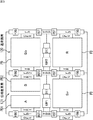
FIG. 4 illustrates the
図5及び図6は、単位画素の構成を示す平面図である。図5は、画角中心部における単位画素の構成を示し、図6は、画角周辺部における単位画素の構成を示している。 5 and 6 are plan views showing the configuration of the unit pixel. FIG. 5 shows the configuration of unit pixels in the center of the angle of view, and FIG. 6 shows the configuration of unit pixels in the periphery of the angle of view.
通常画素120は、光電変換部としてのフォトダイオード(PD)と、複数の画素トランジスタから構成される。フォトダイオード(PD)は、入射光を受光して光電変換し、その光電変換で生成された信号電荷を蓄積する領域を有している。例えば、フォトダイオード(PD)は、N型基板上に形成されたP型ウェル層に対して、P型層を基板表面側に形成してN型埋め込み層を埋め込むことによって形成される埋め込み型のフォトダイオードである。 The normal pixel 120 includes a photodiode (PD) as a photoelectric conversion unit and a plurality of pixel transistors. The photodiode (PD) has a region for receiving incident light, performing photoelectric conversion, and accumulating signal charges generated by the photoelectric conversion. For example, a photodiode (PD) is a buried type formed by embedding an N-type buried layer by forming a P-type layer on the substrate surface side with respect to a P-type well layer formed on an N-type substrate. It is a photodiode.
また、複数の画素トランジスタは、転送トランジスタ(TR)、リセットトランジスタ(RST)、増幅トランジスタ(AMP)、及び、選択トランジスタ(SEL)の4つのトランジスタを有している。転送トランジスタ(TR)は、フォトダイオード(PD)に蓄積された電荷を、浮遊拡散領域(FD:Floating Diffusion)領域に読み出すためのトランジスタである。リセットトランジスタ(RST)は、浮遊拡散領域(FD)の電位を規定の値に設定するためのトランジスタである。増幅トランジスタ(AMP)は、浮遊拡散領域(FD)に読み出された信号電荷を電気的に増幅するためのトランジスタである。選択トランジスタ(SEL)は、画素1行を選択して画素信号を垂直信号線117に読み出すためのトランジスタである。 The plurality of pixel transistors include four transistors: a transfer transistor (TR), a reset transistor (RST), an amplification transistor (AMP), and a selection transistor (SEL). The transfer transistor (TR) is a transistor for reading out charges accumulated in the photodiode (PD) to a floating diffusion region (FD) region. The reset transistor (RST) is a transistor for setting the potential of the floating diffusion region (FD) to a specified value. The amplification transistor (AMP) is a transistor for electrically amplifying the signal charge read to the floating diffusion region (FD). The selection transistor (SEL) is a transistor for selecting one row of pixels and reading a pixel signal to the vertical signal line 117.
容量切り替えトランジスタ(FDG)は、浮遊拡散領域(FD)における変換効率を切り替えるためのトランジスタである。また、オーバフロー制御トランジスタ(OFG)は、オーバフロー制御を実現するためのトランジスタである。 The capacitance switching transistor (FDG) is a transistor for switching the conversion efficiency in the floating diffusion region (FD). The overflow control transistor (OFG) is a transistor for realizing overflow control.
このように、通常画素120は、フォトダイオード(PD)と複数の画素トランジスタを有し、例えば、赤(R)、緑(G)、青(B)のいずれかの色成分信号を画素信号として出力することになる。なお、図5には、通常画素120として、Gb画素、Gr画素,R画素を図示しているが、B画素についても他の色成分に対応する画素と同様の構成を有することになる。 As described above, the normal pixel 120 includes a photodiode (PD) and a plurality of pixel transistors. For example, one of the color component signals of red (R), green (G), and blue (B) is used as the pixel signal. Will be output. In FIG. 5, Gb pixels, Gr pixels, and R pixels are illustrated as the normal pixels 120, but the B pixels also have the same configuration as the pixels corresponding to the other color components.
位相差画素121は、PD分割方式を採用しており、光電変換部としての1つのフォトダイオード(PD)に代えて、それを2分割したような2つのフォトダイオード(PD1,PD2)を有している。なお、以下の説明においても、位相差画素121内の一対の位相差画素のうち、フォトダイオード(PD1)と複数の画素トランジスタから構成される一方の画素を、位相差画素121Aと称し、フォトダイオード(PD2)と複数の画素トランジスタから構成される他方の画素を、位相差画素121Bと称する。すなわち、位相差画素121では、その画素内に、2つのフォトダイオード(PD1,PD2)を形成することで、位相差画素121Aと位相差画素121Bとが一対になって構成されている。
The
位相差画素121Aにおいて、フォトダイオード(PD1)は、入射光を受光して光電変換し、その光電変換で生成された信号電荷を蓄積する領域を有している。例えば、フォトダイオード(PD1)は、通常画素120のフォトダイオード(PD)と同様に、埋め込み型のフォトダイオードとして形成される。また、複数の画素トランジスタは、通常画素120と同様に、転送トランジスタ(TR1)、リセットトランジスタ(RST1)、増幅トランジスタ(AMP1)、及び、選択トランジスタ(SEL1)の4つのトランジスタを有している。 In the phase difference pixel 121A, the photodiode (PD1) has a region for receiving incident light, performing photoelectric conversion, and accumulating signal charges generated by the photoelectric conversion. For example, the photodiode (PD1) is formed as a buried photodiode, like the photodiode (PD) of the normal pixel 120. Further, like the normal pixel 120, the plurality of pixel transistors have four transistors: a transfer transistor (TR1), a reset transistor (RST1), an amplification transistor (AMP1), and a selection transistor (SEL1).
また、位相差画素121Bにおいて、フォトダイオード(PD2)は、入射光を受光して光電変換し、その光電変換で生成された信号電荷を蓄積する領域を有している。例えば、フォトダイオード(PD2)は、通常画素120のフォトダイオード(PD)と同様に、埋め込み型のフォトダイオードとして形成される。また、複数の画素トランジスタは、通常画素120と同様に、転送トランジスタ(TR2)、リセットトランジスタ(RST2)、増幅トランジスタ(AMP2)、及び、選択トランジスタ(SEL2)の4つのトランジスタを有している。 In the phase difference pixel 121B, the photodiode (PD2) has a region for receiving incident light, performing photoelectric conversion, and accumulating signal charges generated by the photoelectric conversion. For example, the photodiode (PD2) is formed as a buried photodiode, like the photodiode (PD) of the normal pixel 120. In addition, like the normal pixel 120, the plurality of pixel transistors include four transistors: a transfer transistor (TR2), a reset transistor (RST2), an amplification transistor (AMP2), and a selection transistor (SEL2).
すなわち、位相差画素121においては、フォトダイオード(PD1)に対する画素トランジスタ(TR1,RST1,AMP1,SEL1)と、フォトダイオード(PD2)に対に対する画素トランジスタ(TR2,RST2,AMP2,SEL2)を別個に設けているため、フォトダイオード(PD1)とフォトダイオード(PD2)における露光と転送を同時に行うことができる。
That is, in the
ここで、図5は、画角中心部における単位画素の構成を示しているため、位相差画素121Aにおけるフォトダイオード(PD1)と、位相差画素121Bにおけるフォトダイオード(PD2)は、同一のサイズの受光面を有している。一方、図6に示すように、画角周辺部における位相差画素121は、画角中心部における位相差画素121と同様に、位相差画素121Aと位相差画素121Bとが一対になって構成されているが、像高に応じて受光面のサイズが変化している。具体的には、位相差画素121Aにおけるフォトダイオード(PD1)の受光面のサイズは、位相差画素121Bにおけるフォトダイオード(PD2)の受光面のサイズよりも小さくなっている。
Here, since FIG. 5 shows the configuration of the unit pixel at the center of the angle of view, the photodiode (PD1) in the phase difference pixel 121A and the photodiode (PD2) in the phase difference pixel 121B have the same size. It has a light receiving surface. On the other hand, as shown in FIG. 6, the
このように、像高に応じて受光面のサイズを変化させることで、集光スポットSが、位相差画素121Aと位相差画素121Bとの境界に設定されることになるが、それに伴い、位相差画素121Aの電荷蓄積領域が、位相差画素121Bの電荷蓄積領域よりも小さくなって、位相差画素121Aの飽和信号量が低下することは先に述べたとおりである。また、先に述べたように、位相差画素121Aと位相差画素121Bのサイズが集光スポットSの位置に応じていく通りにも変化することになるため、その全ての位相差画素121A,121Bの電荷を完全に転送することは容易ではない。 Thus, by changing the size of the light receiving surface according to the image height, the condensing spot S is set at the boundary between the phase difference pixel 121A and the phase difference pixel 121B. As described above, the charge accumulation region of the phase difference pixel 121A becomes smaller than the charge accumulation region of the phase difference pixel 121B, and the saturation signal amount of the phase difference pixel 121A decreases. Further, as described above, since the sizes of the phase difference pixel 121A and the phase difference pixel 121B change according to the position of the focused spot S, all of the phase difference pixels 121A and 121B. It is not easy to completely transfer the charge.
そこで、以下、像高に応じて受光面のサイズを変化させた場合に、位相差画素121A,121Bの飽和信号量の低下を抑制し、かつ、位相差画素121A,121Bの電荷を完全に転送できるようにするための第1の瞳補正方式と第2の瞳補正方式について説明する。 Therefore, hereinafter, when the size of the light receiving surface is changed according to the image height, a decrease in the saturation signal amount of the phase difference pixels 121A and 121B is suppressed, and the charges of the phase difference pixels 121A and 121B are completely transferred. The first pupil correction method and the second pupil correction method for making it possible will be described.
<第1の実施の形態> <First Embodiment>
まず、図7及び図8を参照して、第1の実施の形態としての第1の瞳補正方式について説明する。図7は、図5に示した画角中心部における通常画素120(Gb画素)と位相差画素121の断面図を示し、図8は、図6に示した画角周辺部における通常画素120(Gb画素)と位相差画素121の断面図を示している。
First, the first pupil correction method as the first embodiment will be described with reference to FIGS. 7 shows a cross-sectional view of the normal pixel 120 (Gb pixel) and the
図7に示すように、第1の瞳補正方式では、位相差画素121Aにおけるフォトダイオード(PD1)を、電荷蓄積の主要部となる第1の領域R1と、光電変換をするとともに当該主要部への電荷転送に寄与する第2の領域R2から形成されるようにする。また、位相差画素121Bにおけるフォトダイオード(PD2)についても同様に、第1の領域R1と第2の領域R2から形成されるようにする。ただし、各フォトダイオード(PD1,PD2)においては、不純物濃度を濃淡で表しており、第1の領域R1における不純物濃度は、第2の領域R2における不純物濃度よりも高くなる。また、第2の領域R2は、全体の領域に占める割合が第1の領域R1よりも大きくなる。 As shown in FIG. 7, in the first pupil correction method, the photodiode (PD1) in the phase difference pixel 121A performs photoelectric conversion with the first region R1, which is a main part of charge accumulation, and moves to the main part. The second region R2 that contributes to the charge transfer is formed. Similarly, the photodiode (PD2) in the phase difference pixel 121B is formed of the first region R1 and the second region R2. However, in each photodiode (PD1, PD2), the impurity concentration is represented by shading, and the impurity concentration in the first region R1 is higher than the impurity concentration in the second region R2. Further, the ratio of the second region R2 to the entire region is larger than that of the first region R1.
また、位相差画素121は像高に応じて受光面のサイズを変化させることから、画角中心部では、光の入射側(裏面側)となる第2の領域R2の幅を変える必要はないが、画角周辺部では、第2の領域R2の幅を狭める必要がある。すなわち、図8に示すように、画角周辺部では、位相差画素121Aにおけるフォトダイオード(PD1)の第2の領域R2の幅は、位相差画素121Bにおけるフォトダイオード(PD2)の第2の領域R2の幅よりも狭くなるように形成されている。一方、光の入射側と反対側(表面側)については、画角周辺部では、画角中心部と同様に、フォトダイオード(PD1)の第1の領域R1の幅と、フォトダイオード(PD2)の第1の領域R1の幅が同一になるように形成されている。
Further, since the
すなわち、各画素の素子分離を担っている素子分離部を、裏面側の素子分離部151と表面側の素子分離部152に分けて形成し、素子分離部151は、画角中心部と画角周辺部とで、第2の領域R2の幅を変化させる一方、素子分離部152は、画角中心部と画角周辺部とで、第1の領域R1の幅が同一になるようにする。これにより、各位相差画素121において、像高に応じて受光面のサイズが連続的に変化して、裏面側の第2の領域R2のサイズが変わっても、表面側の第1の領域R1のサイズは変わらないことになる。その結果、不純物濃度の高い第1の領域R1のサイズが不変であることから、画角周辺部においては、画角中心部と比べて、飽和信号量及び転送の容易さに大きな差が生じないことになり、画素アレイ部111に配置された各位相差画素121の特性を一定にすることが可能となる。
In other words, the element isolation part responsible for element isolation of each pixel is formed by dividing it into an
なお、素子分離部151と素子分離部152は、例えば、金属、酸化膜、又は不純物などにより形成することができる。
Note that the
以上、第1の瞳補正方式では、図7の画角中心部では、位相差画素121Aと位相差画素121Bにおいて、第1の領域R1及び第2の領域R2ともに同一の構成とし、図8の画角周辺部では、第2の領域R2の構成は異なるが、第1の領域R1は同一の構成とすることで、飽和信号量及び転送の容易さに大きな差を生じさせないようにして、画素アレイ部111に配置された各位相差画素121の特性を一定にさせている。
As described above, in the first pupil correction method, the first region R1 and the second region R2 have the same configuration in the phase difference pixel 121A and the phase difference pixel 121B in the center of the angle of view in FIG. In the periphery of the angle of view, the configuration of the second region R2 is different, but the first region R1 has the same configuration so as not to cause a large difference in the saturation signal amount and the ease of transfer. The characteristics of the respective
<第2の実施の形態> <Second Embodiment>
次に、図9及び図10を参照して、第2の実施の形態としての第2の瞳補正方式について説明する。図9は、図5に示した画角中心部における通常画素120(Gb画素)と位相差画素121の平面図を示し、図10は、図6に示した画角周辺部における通常画素120(Gb画素)と位相差画素121の平面図を示している。
Next, the second pupil correction method as the second embodiment will be described with reference to FIGS. FIG. 9 is a plan view of the normal pixel 120 (Gb pixel) and the
図9に示すように、第2の瞳補正方式では、第1の瞳補正方式と同様に、位相差画素121Aにおけるフォトダイオード(PD1)を、電荷蓄積の主要部となる第1の領域R1と、光電変換するとともに当該主要部への電荷転送に寄与する第2の領域R2から形成されるようにする。また、位相差画素121Bにおけるフォトダイオード(PD2)についても同様に、第1の領域R1と第2の領域R2から形成されるようにする。なお、図9及び図10においては、図7及び図8と同様に、各フォトダイオード(PD1,PD2)における不純物濃度を濃淡で表している。 As shown in FIG. 9, in the second pupil correction method, as in the first pupil correction method, the photodiode (PD1) in the phase difference pixel 121A is connected to the first region R1 that is a main part of charge accumulation. The second region R2 is formed from the second region R2 that performs photoelectric conversion and contributes to charge transfer to the main part. Similarly, the photodiode (PD2) in the phase difference pixel 121B is formed of the first region R1 and the second region R2. In FIGS. 9 and 10, the impurity concentration in each photodiode (PD1, PD2) is represented by shading as in FIGS.
また、位相差画素121Aにおいて、転送トランジスタ(TR1)は、位相差画素121Aと位相差画素121Bとを分割した方向と平行であって、フォトダイオード(PD1)の受光面の中心から最も近い位置の近傍に配置される。これにより、転送トランジスタ(TR1)の近傍の領域の不純物濃度が、他の領域の不純物濃度よりも高くなる。同様に、位相差画素121Bにおいて、転送トランジスタ(TR2)は、位相差画素121Aと位相差画素121Bとを分割した方向と平行であって、フォトダイオード(PD2)の受光面の中心から最も近い位置の近傍に配置される。これにより、転送トランジスタ(TR2)の近傍の領域の不純物濃度が、他の領域の不純物濃度よりも高くなる。 In the phase difference pixel 121A, the transfer transistor (TR1) is parallel to the direction in which the phase difference pixel 121A and the phase difference pixel 121B are divided, and is located closest to the center of the light receiving surface of the photodiode (PD1). Located in the vicinity. As a result, the impurity concentration in the region near the transfer transistor (TR1) is higher than the impurity concentration in other regions. Similarly, in the phase difference pixel 121B, the transfer transistor (TR2) is parallel to the direction in which the phase difference pixel 121A and the phase difference pixel 121B are divided and is closest to the center of the light receiving surface of the photodiode (PD2). It is arranged in the vicinity of As a result, the impurity concentration in the region near the transfer transistor (TR2) is higher than the impurity concentration in other regions.
また、位相差画素121は像高に応じて受光面のサイズを変化させることから、画角中心部では受光面のサイズを変える必要はないが、画角周辺部では受光面のサイズを変化させる必要がある。すなわち、図10に示すように、画角周辺部では、位相差画素121Aにおける受光面のサイズは、位相差画素121Bにおける受光面のサイズよりも小さくなっている。しかしながら、画角周辺部においては、画角中心部と同様に転送トランジスタ(TR1,TR2)を配置することで、それらの転送トランジスタ(TR1,TR2)の近傍の領域の不純物濃度は、他の領域の不純物濃度よりも高くなっている。
Since the
すなわち、各位相差画素121において、像高に応じて受光面のサイズが連続的に変化して、例えば、位相差画素121Aにおける受光面のサイズが小さくなっても、不純物濃度の高い第1の領域R1が転送トランジスタ(TR1)の近傍の領域に形成されることは不変である。その結果、不純物濃度の高い第1の領域R1はサイズの変化の影響を受けないことから、画角周辺部においては、画角中心部と比べて、飽和信号量及び転送の容易さに大きな差が生じないこととなり、画素アレイ部111に配置された各位相差画素121の特性を一定にすることができる。
That is, in each
以上、第2の瞳補正方式では、図9の画角中心部と図10の画角周辺部では、受光面のサイズは変化しているものの、転送トランジスタ(TR1,TR2)の近傍の構造を同一の構成とし、転送トランジスタ(TR1,TR2)の近傍の領域の不純物濃度を他の領域よりも高くなるようにすることで、飽和信号量及び転送の容易さに大きな差を生じさせないようにして、画素アレイ部111に配置された各位相差画素121の特性を一定にさせている。
As described above, in the second pupil correction method, the structure of the vicinity of the transfer transistors (TR1, TR2) is changed in the central part of the angle of view in FIG. 9 and the peripheral part of the angle of view in FIG. By adopting the same configuration and making the impurity concentration in the region near the transfer transistors (TR1, TR2) higher than in other regions, it does not cause a large difference in saturation signal amount and ease of transfer. The characteristics of each
以上のように、本技術によれば、画素アレイ部111に配置された各位相差画素121において、像高に応じて受光面のサイズを連続的に変化させるに際し、不純物濃度の高い第1の領域R1がその変化の影響を受けないようにすることで、画角周辺部においては、画角中心部と比べて、飽和信号量及び転送の容易さに大きな差が生じないことになり、各位相差画素121の特性を一定にすることが可能となる。すなわち、各位相差画素121においては、電荷蓄積の主要部が同一の構造となるため、瞳補正と飽和信号量の低下の抑制を両立するとともに、電荷転送を同様に行うことができるようになる。
As described above, according to the present technology, in each of the
また、位相差画素121では、1画素内に、位相差画素121Aと位相差画素121Bとが一対になって搭載されていることから、容易に、画素アレイ部111に配置される位相差画素121の数を多くして、位相差画素121の特性を向上させることができる。また、レンズの瞳補正に応じて像高によって、位相差画素121A,121Bのサイズを変化させることから、結果として、像面位相差AFに対応可能な交換レンズを増加させることができる。
Further, in the
なお、上述した説明では、画素アレイ部111に、行状に配列された位相差画素121について説明したが、本技術は、位相差画素121を列状に配置した場合にも適用することができる。この場合においても、位相差画素121A,121Bは、画角中心部において同一のサイズの受光面を有することになるが、画角周辺部においては像高に応じて受光面のサイズが変化することになる。具体的には、例えば、図4に示した行状に配置した複数の位相差画素121を、画角中心部の位相差画素121を中心に、反時計回りに90度回転させた状態の受光面のサイズを各位相差画素121が有するように構成されることになる。
In the above description, the
また、本技術は、固体撮像素子への適用に限られるものではない。すなわち、本技術は、デジタルカメラ等の撮像装置や、撮像機能を有する携帯端末装置や、画像読取部に固体撮像素子を用いる複写機など、画像取込部(光電変換部)に固体撮像素子を用いる電子機器全般に対して適用可能である。また、固体撮像素子は、ワンチップとして形成された形態であってもよいし、撮像部と信号処理部又は光学系とがまとめてパッケージングされた撮像機能を有するモジュール状の形態であってもよい。 Further, the present technology is not limited to application to a solid-state imaging device. That is, the present technology provides a solid-state imaging device for an image capturing unit (photoelectric conversion unit) such as an imaging device such as a digital camera, a portable terminal device having an imaging function, and a copying machine using a solid-state imaging device for an image reading unit. Applicable to all electronic devices used. In addition, the solid-state imaging device may be formed as a single chip, or may be a module-shaped configuration having an imaging function in which an imaging unit and a signal processing unit or an optical system are packaged together. Good.
<本技術を適用した電子機器の構成例> <Configuration example of electronic equipment to which this technology is applied>
図11は、本技術を適用した電子機器の一実施の形態の構成を示すブロック図である。 FIG. 11 is a block diagram illustrating a configuration of an embodiment of an electronic device to which the present technology is applied.
図11に示すように、電子機器としての撮像装置300は、レンズ群などからなる光学部301、上述した単位画素120の各構成が採用される固体撮像素子302、及び、カメラ信号処理回路であるDSP(Digital Signal Processor)回路303を備える。また、撮像装置300は、フレームメモリ304、表示部305、記録部306、操作部307、電源部308、及び、制御部309も備える。DSP回路303、フレームメモリ304、表示部305、記録部306、操作部307、電源部308、及び、制御部309は、バスライン310を介して相互に接続されている。
As illustrated in FIG. 11, an imaging apparatus 300 as an electronic device includes an
光学部301は、被写体からの入射光(像光)を取り込んで固体撮像素子302の撮像面上に結像する。固体撮像素子302は、光学部301によって撮像面上に結像された入射光の光量を画素単位で電気信号に変換して、被写体の像を示す画像信号を形成するための色成分信号を画素信号として出力する。また、固体撮像素子302は、像面位相差AFに用いられる位相差検出用信号を画素信号として出力する。この固体撮像素子302として、上述した実施の形態に係るCMOSイメージセンサ100等の固体撮像素子、すなわち、画素アレイ部111に配置された各位相差画素121の特性を一定にすることができる固体撮像素子を用いることができる。
The
表示部305は、例えば、液晶パネルや有機EL(electro luminescence)パネル等のパネル型表示装置からなり、固体撮像素子302で撮像された静止画又は動画を表示する。記録部306は、固体撮像素子302で撮像された静止画又は動画のデータを、フラッシュメモリ等の記録媒体に記録する。
The
操作部307は、ユーザによる操作に従い、撮像装置300が持つ様々な機能について操作指令を発する。電源部308は、DSP回路303、フレームメモリ304、表示部305、記録部306、操作部307、及び、制御部309の動作電源となる各種の電源を、これら供給対象に対して適宜供給する。
The
制御部309は、撮像装置300の各部の動作を制御する。また、制御部309は、固体撮像素子302からの位相差検出用信号を用いた所定の演算を行うことでデフォーカス量を算出し、このデフォーカス量に応じて合焦状態になるように、光学部301に含まれる撮影レンズなどの駆動を制御する。これにより、像面位相差AFが行われ、被写体にピントが合わせられる。
The
なお、上述した実施の形態においては、可視光の光量に応じた信号電荷を物理量として検知する単位画素が行列状に配置されてなるCMOSイメージセンサに適用した場合を例に挙げて説明した。しかしながら、本技術はCMOSイメージセンサへの適用に限られるものではなく、画素アレイ部の画素列ごとにカラム処理部を配置してなるカラム方式の固体撮像素子全般に対して適用可能である。 In the above-described embodiment, the case where the present invention is applied to a CMOS image sensor in which unit pixels that detect signal charges corresponding to the amount of visible light as physical quantities are arranged in a matrix has been described as an example. However, the present technology is not limited to application to a CMOS image sensor, and can be applied to all column-type solid-state imaging devices in which a column processing unit is arranged for each pixel column of a pixel array unit.
また、本技術は、可視光の入射光量の分布を検知して画像として撮像する固体撮像素子への適用に限らず、赤外線やX線、あるいは粒子等の入射量の分布を画像として撮像する固体撮像素子や、広義の意味として、圧力や静電容量など、他の物理量の分布を検知して画像として撮像する指紋検出センサ等の固体撮像素子(物理量分布検知装置)全般に対して適用可能である。 In addition, the present technology is not limited to application to a solid-state imaging device that detects the distribution of the amount of incident light of visible light and captures it as an image, but a solid-state that captures the distribution of the incident amount of infrared rays, X-rays, particles, or the like as an image. Applicable to imaging devices and, in a broad sense, solid-state imaging devices (physical quantity distribution detection devices) such as fingerprint detection sensors that detect the distribution of other physical quantities such as pressure and capacitance and capture images as images. is there.
なお、本技術の実施の形態は、上述した実施の形態に限定されるものではなく、本技術の要旨を逸脱しない範囲において種々の変更が可能である。 The embodiments of the present technology are not limited to the above-described embodiments, and various modifications can be made without departing from the gist of the present technology.
また、本技術は、以下のような構成をとることができる。 Moreover, this technique can take the following structures.
(1)
入射光を受光して光電変換する光電変換部を有し、色成分信号が得られる第1の画素と、
受光面が像高に応じたサイズからなる一対の第1の光電変換部と第2の光電変換部を有し、位相差検出用信号が得られる第2の画素と
を行列状に配置した画素アレイ部を備え、
一対の前記第1の光電変換部と前記第2の光電変換部は、電荷蓄積の主要部となる第1の領域と、光電変換をするとともに前記主要部への電荷転送に寄与する第2の領域をそれぞれ有している
固体撮像素子。
(2)
一対の前記第1の光電変換部と前記第2の光電変換部において、光の入射側となる前記第2の領域は瞳補正に応じたサイズとなり、光の入射側の反対側となる前記第1の領域は同一のサイズとなる
(1)に記載の固体撮像素子。
(3)
前記第1の領域における不純物濃度は、前記第2の領域における不純物濃度よりも高くなる
(2)に記載の固体撮像素子。
(4)
前記第2の領域は、前記第1の領域よりも大きくなる
(3)に記載の固体撮像素子。
(5)
前記第1の光電変換部に蓄積された電荷を転送する第1の転送トランジスタと、
前記第2の光電変換部に蓄積された電荷を転送する第2の転送トランジスタと
をさらに有し、
一対の前記第1の光電変換部と前記第2の光電変換部において、前記第1の転送トランジスタの近傍の領域と、前記第2の転送トランジスタの近傍の領域の不純物濃度は、他の領域の不純物濃度よりも高くなる
(1)に記載の固体撮像素子。
(6)
前記第1の転送トランジスタは、前記第1の光電変換部の受光面の中心から最も近い位置の近傍に配置され、
前記第2の転送トランジスタは、前記第2の光電変換部の受光面の中心から最も近い位置の近傍に配置される
(5)に記載の固体撮像素子。
(7)
前記第1の転送トランジスタによって前記第1の光電変換部から転送される電荷を信号として読み出すために保持する第1の浮遊拡散領域と、
前記第2の転送トランジスタによって前記第2の光電変換部から転送される電荷を信号として読み出すために保持する第2の浮遊拡散領域と
をさらに有する(6)に記載の固体撮像素子。
(8)
前記第1の光電変換部と前記第2の光電変換部における露光と転送を同時に行う
(1)乃至(7)のいずれか一項に記載の固体撮像素子。
(9)
一対の前記第1の光電変換部と前記第2の光電変換部は、その分離部が連続的に変化する
(1)乃至(8)のいずれか一項に記載の固体撮像素子。
(10)
一対の前記第1の光電変換部と前記第2の光電変換部は、金属、酸化膜、又は不純物により分離されている
(1)乃至(9)のいずれか一項に記載の固体撮像素子。
(11)
入射光を受光して光電変換する光電変換部を有し、色成分信号が得られる第1の画素と、
受光面が像高に応じたサイズからなる一対の第1の光電変換部と第2の光電変換部を有し、位相差検出用信号が得られる第2の画素と
を行列状に配置した画素アレイ部を備え、
一対の前記第1の光電変換部と前記第2の光電変換部は、電荷蓄積の主要部となる第1の領域と、光電変換をするとともに前記主要部への電荷転送に寄与する第2の領域をそれぞれ有している
固体撮像素子の駆動方法において、
画素駆動部が、一対の前記第1の光電変換部と前記第2の光電変換部を別個に駆動して、前記第1の光電変換部と前記第2の光電変換部における露光と転送を同時に行うステップ
を含む駆動方法。
(12)
入射光を受光して光電変換する光電変換部を有し、色成分信号が得られる第1の画素と、
受光面が像高に応じたサイズからなる一対の第1の光電変換部と第2の光電変換部を有し、位相差検出用信号が得られる第2の画素と
を行列状に配置した画素アレイ部を備え、
一対の前記第1の光電変換部と前記第2の光電変換部は、電荷蓄積の主要部となる第1の領域と、光電変換をするとともに前記主要部への電荷転送に寄与する第2の領域をそれぞれ有している
固体撮像素子を搭載し、
前記固体撮像素子から出力される前記位相差検出用信号を用いて、像面位相差AF(Autofocus)を制御する制御部を備える
電子機器。
(1)
A first pixel that has a photoelectric conversion unit that receives incident light and performs photoelectric conversion, and obtains a color component signal;
A pixel in which a light receiving surface has a pair of first and second photoelectric conversion units each having a size corresponding to an image height, and second pixels from which phase difference detection signals are obtained are arranged in a matrix. It has an array part,
The pair of the first photoelectric conversion unit and the second photoelectric conversion unit are a first region that is a main part of charge accumulation and a second region that performs photoelectric conversion and contributes to charge transfer to the main part. A solid-state image sensor having regions.
(2)
In the pair of the first photoelectric conversion unit and the second photoelectric conversion unit, the second region on the light incident side has a size corresponding to pupil correction, and the second region on the opposite side of the light incident side. The area | region of 1 becomes the same size. The solid-state image sensor as described in (1).
(3)
The solid-state imaging device according to (2), wherein the impurity concentration in the first region is higher than the impurity concentration in the second region.
(4)
The solid-state imaging device according to (3), wherein the second region is larger than the first region.
(5)
A first transfer transistor that transfers charges accumulated in the first photoelectric conversion unit;
A second transfer transistor that transfers the charge accumulated in the second photoelectric conversion unit, and
In the pair of the first photoelectric conversion unit and the second photoelectric conversion unit, the impurity concentration in the region in the vicinity of the first transfer transistor and the region in the vicinity of the second transfer transistor is different from that in other regions. The solid-state imaging device according to (1), which is higher than the impurity concentration.
(6)
The first transfer transistor is disposed in the vicinity of the position closest to the center of the light receiving surface of the first photoelectric conversion unit,
The solid-state imaging device according to (5), wherein the second transfer transistor is disposed in a vicinity of a position closest to a center of a light receiving surface of the second photoelectric conversion unit.
(7)
A first floating diffusion region for holding the charge transferred from the first photoelectric conversion unit by the first transfer transistor for reading as a signal;
The solid-state imaging device according to (6), further including: a second floating diffusion region that holds the charge transferred from the second photoelectric conversion unit by the second transfer transistor as a signal.
(8)
The solid-state imaging device according to any one of (1) to (7), wherein exposure and transfer in the first photoelectric conversion unit and the second photoelectric conversion unit are performed simultaneously.
(9)
The solid-state imaging device according to any one of (1) to (8), wherein a separation unit of the pair of the first photoelectric conversion unit and the second photoelectric conversion unit is continuously changed.
(10)
A pair of said 1st photoelectric conversion part and said 2nd photoelectric conversion part are isolate | separated by the metal, the oxide film, or the impurity. The solid-state image sensor as described in any one of (1) thru | or (9).
(11)
A first pixel that has a photoelectric conversion unit that receives incident light and performs photoelectric conversion, and obtains a color component signal;
A pixel in which a light receiving surface has a pair of first and second photoelectric conversion units each having a size corresponding to an image height, and second pixels from which phase difference detection signals are obtained are arranged in a matrix. It has an array part,
The pair of the first photoelectric conversion unit and the second photoelectric conversion unit are a first region that is a main part of charge accumulation and a second region that performs photoelectric conversion and contributes to charge transfer to the main part. In the driving method of the solid-state imaging device having each region,
The pixel driving unit separately drives the pair of the first photoelectric conversion unit and the second photoelectric conversion unit, and simultaneously performs exposure and transfer in the first photoelectric conversion unit and the second photoelectric conversion unit. A driving method including the step of performing.
(12)
A first pixel that has a photoelectric conversion unit that receives incident light and performs photoelectric conversion, and obtains a color component signal;
A pixel in which a light receiving surface has a pair of first and second photoelectric conversion units each having a size corresponding to an image height, and second pixels from which phase difference detection signals are obtained are arranged in a matrix. It has an array part,
The pair of the first photoelectric conversion unit and the second photoelectric conversion unit are a first region that is a main part of charge accumulation and a second region that performs photoelectric conversion and contributes to charge transfer to the main part. Equipped with a solid-state image sensor that has each area,
An electronic apparatus comprising a control unit that controls an image plane phase difference AF (Autofocus) using the phase difference detection signal output from the solid-state imaging device.
100 CMOSイメージセンサ, 111 画素アレイ部, 120 通常画素, 121,121A,121B 位相差画素, 151,152 素子分離部, 300 撮像装置, 302 固体撮像素子, 309 制御部, R1 第1の領域, R2 第2の領域, PD,PD1,PD2 フォトダイオード, TR,TR1,TR2 転送トランジスタ, RST,RST1,RST2 リセットトランジスタ, AMP,AMP1,AMP2 増幅トランジスタ, SEL,SEL1,SEL2 選択トランジスタ, FDG,FDG1,FDG2 容量切り替えトランジスタ 100 CMOS image sensor, 111 pixel array unit, 120 normal pixel, 121, 121A, 121B phase difference pixel, 151, 152 element separation unit, 300 imaging device, 302 solid-state imaging device, 309 control unit, R1 first region, R2 Second region, PD, PD1, PD2 photodiode, TR, TR1, TR2 transfer transistor, RST, RST1, RST2 reset transistor, AMP, AMP1, AMP2 amplification transistor, SEL, SEL1, SEL2 selection transistor, FDG, FDG1, FDG2 Capacitance switching transistor
Claims (8)
一対の第1の光電変換部と第2の光電変換部を有し、位相差検出用信号が得られる第2の画素と
を行列状に配置した画素アレイ部を備え、
一対の前記第1の光電変換部と前記第2の光電変換部は、電荷蓄積の主要部となる第1の領域と、光電変換をするとともに前記主要部への電荷転送に寄与する第2の領域をそれぞれ有し、
一対の前記第1の光電変換部と前記第2の光電変換部において、光の入射側となる前記第2の領域は、集光スポットが前記第1の光電変換部と前記第2の光電変換部との境界に設定されるように、像高に応じたサイズとなり、光の入射側の反対側となる前記第1の領域は、同一のサイズとなる
固体撮像素子。 A first pixel that has a photoelectric conversion unit that receives incident light and performs photoelectric conversion, and obtains a color component signal;
A pixel array unit having a pair of first photoelectric conversion units and second photoelectric conversion units, and second pixels from which phase difference detection signals are obtained are arranged in a matrix;
The pair of the first photoelectric conversion unit and the second photoelectric conversion unit are a first region that is a main part of charge accumulation and a second region that performs photoelectric conversion and contributes to charge transfer to the main part. Each has a region ,
In the pair of the first photoelectric conversion unit and the second photoelectric conversion unit, the second region on the light incident side has a condensing spot as the first photoelectric conversion unit and the second photoelectric conversion unit. A solid-state imaging device having a size corresponding to the image height so that the first region on the opposite side of the light incident side has the same size as set at the boundary with the unit .
請求項1に記載の固体撮像素子。 The impurity concentration in the first region, the solid-state imaging device according to claim 1 which is higher than the impurity concentration in the second region.
請求項2に記載の固体撮像素子。 The solid-state imaging device according to claim 2 , wherein the second region is larger than the first region.
請求項1乃至3のいずれかに記載の固体撮像素子。 Solid-state imaging device according to any one of claims 1 to 3 transfers the exposure in the second photoelectric conversion unit and the first photoelectric conversion section at the same time.
請求項1乃至4のいずれかに記載の固体撮像素子。 To said second photoelectric conversion portion and a pair of the first photoelectric conversion unit, the separation unit is, depending on the image height, is formed at a position so as to continuously change the width of the second region solid-state imaging device according to any one of claims 1 to 4 that.
請求項5のいずれかに記載の固体撮像素子。 The solid-state imaging device according to claim 5 , wherein the pair of the first photoelectric conversion unit and the second photoelectric conversion unit are separated by a metal, an oxide film, or an impurity.
一対の第1の光電変換部と第2の光電変換部を有し、位相差検出用信号が得られる第2の画素と
を行列状に配置した画素アレイ部を備え、
一対の前記第1の光電変換部と前記第2の光電変換部は、電荷蓄積の主要部となる第1の領域と、光電変換をするとともに前記主要部への電荷転送に寄与する第2の領域をそれぞれ有し、
一対の前記第1の光電変換部と前記第2の光電変換部において、光の入射側となる前記第2の領域は、集光スポットが前記第1の光電変換部と前記第2の光電変換部との境界に設定されるように、像高に応じたサイズとなり、光の入射側の反対側となる前記第1の領域は、同一のサイズとなる
固体撮像素子の駆動方法において、
画素駆動部が、一対の前記第1の光電変換部と前記第2の光電変換部を別個に駆動して、前記第1の光電変換部と前記第2の光電変換部における露光と転送を同時に行うステップ
を含む駆動方法。 A first pixel that has a photoelectric conversion unit that receives incident light and performs photoelectric conversion, and obtains a color component signal;
A pixel array unit having a pair of first photoelectric conversion units and second photoelectric conversion units, and second pixels from which phase difference detection signals are obtained are arranged in a matrix;
The pair of the first photoelectric conversion unit and the second photoelectric conversion unit are a first region that is a main part of charge accumulation and a second region that performs photoelectric conversion and contributes to charge transfer to the main part. Each has a region ,
In the pair of the first photoelectric conversion unit and the second photoelectric conversion unit, the second region on the light incident side has a condensing spot as the first photoelectric conversion unit and the second photoelectric conversion unit. In the driving method of the solid-state imaging device , the first area which is the size corresponding to the image height and is opposite to the light incident side is set to the boundary with the unit ,
The pixel driving unit separately drives the pair of the first photoelectric conversion unit and the second photoelectric conversion unit, and simultaneously performs exposure and transfer in the first photoelectric conversion unit and the second photoelectric conversion unit. A driving method including the step of performing.
一対の第1の光電変換部と第2の光電変換部を有し、位相差検出用信号が得られる第2の画素と
を行列状に配置した画素アレイ部を備え、
一対の前記第1の光電変換部と前記第2の光電変換部は、電荷蓄積の主要部となる第1の領域と、光電変換をするとともに前記主要部への電荷転送に寄与する第2の領域をそれぞれ有し、
一対の前記第1の光電変換部と前記第2の光電変換部において、光の入射側となる前記第2の領域は、集光スポットが前記第1の光電変換部と前記第2の光電変換部との境界に設定されるように、像高に応じたサイズとなり、光の入射側の反対側となる前記第1の領域は、同一のサイズとなる
固体撮像素子を搭載し、
前記固体撮像素子から出力される前記位相差検出用信号を用いて、像面位相差AF(Autofocus)を制御する制御部を備える
電子機器。 A first pixel that has a photoelectric conversion unit that receives incident light and performs photoelectric conversion, and obtains a color component signal;
A pixel array unit having a pair of first photoelectric conversion units and second photoelectric conversion units, and second pixels from which phase difference detection signals are obtained are arranged in a matrix;
The pair of the first photoelectric conversion unit and the second photoelectric conversion unit are a first region that is a main part of charge accumulation and a second region that performs photoelectric conversion and contributes to charge transfer to the main part. Each has a region ,
In the pair of the first photoelectric conversion unit and the second photoelectric conversion unit, the second region on the light incident side has a condensing spot as the first photoelectric conversion unit and the second photoelectric conversion unit. The first region which is the size corresponding to the image height and is opposite to the light incident side is mounted with a solid-state imaging device having the same size, so as to be set at the boundary with the unit ,
An electronic apparatus comprising a control unit that controls an image plane phase difference AF (Autofocus) using the phase difference detection signal output from the solid-state imaging device.
Priority Applications (10)
| Application Number | Priority Date | Filing Date | Title |
|---|---|---|---|
| JP2013197872A JP6127869B2 (en) | 2013-09-25 | 2013-09-25 | Solid-state imaging device, driving method thereof, and electronic apparatus |
| TW103130294A TWI663877B (en) | 2013-09-25 | 2014-09-02 | Solid-state imaging element, driving method thereof, and electronic device |
| CN201710014175.1A CN107068702B (en) | 2013-09-25 | 2014-09-12 | Solid-state imaging device and electronic apparatus |
| CN201480048428.1A CN105518862B (en) | 2013-09-25 | 2014-09-12 | The driving method and electronic device of solid imaging element, solid imaging element |
| KR1020167007217A KR101857377B1 (en) | 2013-09-25 | 2014-09-12 | Solid state imaging element, drive method therefor, and electronic device |
| US15/022,478 US9706145B2 (en) | 2013-09-25 | 2014-09-12 | Solid-state imaging element and driving method therefor, and electronic apparatus |
| PCT/JP2014/074245 WO2015045915A1 (en) | 2013-09-25 | 2014-09-12 | Solid state imaging element, drive method therefor, and electronic device |
| CN201710012765.0A CN106888358B (en) | 2013-09-25 | 2014-09-12 | Solid-state imaging device, driving method of solid-state imaging device, and electronic apparatus |
| US15/587,035 US9888196B2 (en) | 2013-09-25 | 2017-05-04 | Solid-state imaging element and driving method therefor, and electronic apparatus |
| US15/815,415 US10015426B2 (en) | 2013-09-25 | 2017-11-16 | Solid-state imaging element and driving method therefor, and electronic apparatus |
Applications Claiming Priority (1)
| Application Number | Priority Date | Filing Date | Title |
|---|---|---|---|
| JP2013197872A JP6127869B2 (en) | 2013-09-25 | 2013-09-25 | Solid-state imaging device, driving method thereof, and electronic apparatus |
Publications (3)
| Publication Number | Publication Date |
|---|---|
| JP2015065269A JP2015065269A (en) | 2015-04-09 |
| JP2015065269A5 JP2015065269A5 (en) | 2016-03-17 |
| JP6127869B2 true JP6127869B2 (en) | 2017-05-17 |
Family
ID=52743057
Family Applications (1)
| Application Number | Title | Priority Date | Filing Date |
|---|---|---|---|
| JP2013197872A Active JP6127869B2 (en) | 2013-09-25 | 2013-09-25 | Solid-state imaging device, driving method thereof, and electronic apparatus |
Country Status (6)
| Country | Link |
|---|---|
| US (3) | US9706145B2 (en) |
| JP (1) | JP6127869B2 (en) |
| KR (1) | KR101857377B1 (en) |
| CN (3) | CN105518862B (en) |
| TW (1) | TWI663877B (en) |
| WO (1) | WO2015045915A1 (en) |
Families Citing this family (26)
| Publication number | Priority date | Publication date | Assignee | Title |
|---|---|---|---|---|
| KR20150121564A (en) * | 2014-04-21 | 2015-10-29 | 삼성전자주식회사 | Imaging device and photographing apparatus |
| KR102449720B1 (en) * | 2015-10-12 | 2022-09-29 | 삼성전자주식회사 | Method and apparatus for certification using image sensor |
| TWI731017B (en) | 2016-01-27 | 2021-06-21 | 日商新力股份有限公司 | Solid-state imaging device and electronic equipment |
| CN111741200B (en) | 2016-04-08 | 2021-12-21 | 佳能株式会社 | Image sensor and image pickup apparatus |
| JP6774207B2 (en) * | 2016-04-08 | 2020-10-21 | キヤノン株式会社 | Image sensor and image sensor |
| JP7005125B2 (en) | 2016-04-22 | 2022-01-21 | キヤノン株式会社 | Image sensor, image sensor, and method for manufacturing the image sensor |
| KR20180024604A (en) | 2016-08-30 | 2018-03-08 | 삼성전자주식회사 | Image sensor and driving method thereof |
| WO2018061497A1 (en) * | 2016-09-27 | 2018-04-05 | 富士フイルム株式会社 | Imaging element and imaging device |
| CN115763507A (en) * | 2016-10-28 | 2023-03-07 | 索尼公司 | Photodetector and electronic device |
| KR102574236B1 (en) * | 2016-12-07 | 2023-09-05 | 에스케이하이닉스 주식회사 | Image Sensor Including Photodiodes Having Different Sizes with Each Other |
| TWI754696B (en) * | 2016-12-14 | 2022-02-11 | 日商索尼半導體解決方案公司 | Solid-state imaging elements and electronic devices |
| JP6877166B2 (en) * | 2017-02-10 | 2021-05-26 | ユナイテッド・セミコンダクター・ジャパン株式会社 | Semiconductor devices and their manufacturing methods |
| JP6932580B2 (en) * | 2017-08-04 | 2021-09-08 | ソニーセミコンダクタソリューションズ株式会社 | Solid-state image sensor |
| US10714517B2 (en) * | 2018-01-23 | 2020-07-14 | Samsung Electronics Co., Ltd. | Image sensor |
| US11658193B2 (en) | 2018-01-23 | 2023-05-23 | Samsung Electronics Co., Ltd. | Image sensor |
| JP2019140219A (en) * | 2018-02-09 | 2019-08-22 | ソニーセミコンダクタソリューションズ株式会社 | Semiconductor device and manufacturing method of semiconductor device |
| KR102532003B1 (en) * | 2018-10-31 | 2023-05-15 | 에스케이하이닉스 주식회사 | Image Sensor Having 2-colored Color Filters Sharing one Photodiode |
| CN109713002B (en) * | 2018-12-07 | 2021-08-31 | 德淮半导体有限公司 | Image sensor and forming method thereof |
| JP2020113573A (en) | 2019-01-08 | 2020-07-27 | キヤノン株式会社 | Photoelectric conversion device |
| KR102519712B1 (en) | 2019-01-18 | 2023-04-06 | 삼성전자주식회사 | Image sensor |
| CN110062144A (en) * | 2019-05-14 | 2019-07-26 | 德淮半导体有限公司 | Phase focus image sensor and forming method thereof, working method |
| CN110233961B (en) * | 2019-07-30 | 2021-03-05 | Oppo广东移动通信有限公司 | Complementary metal oxide image sensor and terminal |
| JP2021068788A (en) | 2019-10-21 | 2021-04-30 | キヤノン株式会社 | Photoelectric conversion device, manufacturing method of the same, and imaging system |
| KR20210047483A (en) * | 2019-10-22 | 2021-04-30 | 에스케이하이닉스 주식회사 | Image sensor for supporting plural capturing modes |
| JP2020188267A (en) * | 2020-07-14 | 2020-11-19 | キヤノン株式会社 | Imaging device |
| KR20220139740A (en) | 2021-04-08 | 2022-10-17 | 삼성전자주식회사 | Image sensor including auto-focus pixel |
Family Cites Families (24)
| Publication number | Priority date | Publication date | Assignee | Title |
|---|---|---|---|---|
| JP2500428B2 (en) * | 1993-04-06 | 1996-05-29 | 日本電気株式会社 | Image sensor and driving method thereof |
| US6563105B2 (en) * | 1999-06-08 | 2003-05-13 | University Of Washington | Image acquisition with depth enhancement |
| US6750437B2 (en) * | 2000-08-28 | 2004-06-15 | Canon Kabushiki Kaisha | Image pickup apparatus that suitably adjusts a focus |
| JP2004165462A (en) | 2002-11-14 | 2004-06-10 | Sony Corp | Solid-state imaging device and its manufacturing method |
| JP2006294871A (en) * | 2005-04-11 | 2006-10-26 | Matsushita Electric Ind Co Ltd | Solid-state imaging apparatus |
| JP5002412B2 (en) * | 2007-10-24 | 2012-08-15 | キヤノン株式会社 | Imaging device |
| US8482639B2 (en) * | 2008-02-08 | 2013-07-09 | Omnivision Technologies, Inc. | Black reference pixel for backside illuminated image sensor |
| JP5552214B2 (en) * | 2008-03-11 | 2014-07-16 | キヤノン株式会社 | Focus detection device |
| JP5451111B2 (en) * | 2008-03-11 | 2014-03-26 | キヤノン株式会社 | Focus detection apparatus and imaging apparatus having the same |
| JP5098831B2 (en) * | 2008-06-06 | 2012-12-12 | ソニー株式会社 | Solid-state imaging device and camera system |
| JP5276371B2 (en) * | 2008-07-09 | 2013-08-28 | キヤノン株式会社 | Imaging device |
| JP5537172B2 (en) * | 2010-01-28 | 2014-07-02 | ソニー株式会社 | Solid-state imaging device and electronic apparatus |
| TW201200959A (en) * | 2010-06-29 | 2012-01-01 | Fujifilm Corp | One-eyed stereo photographic device |
| JP2012023207A (en) * | 2010-07-14 | 2012-02-02 | Toshiba Corp | Backside-illuminated solid-state imaging device |
| JP2012084816A (en) | 2010-10-14 | 2012-04-26 | Fujifilm Corp | Back surface irradiation type imaging device and imaging apparatus |
| JP5753371B2 (en) * | 2010-11-25 | 2015-07-22 | キヤノン株式会社 | Imaging apparatus and control method thereof |
| JP5866760B2 (en) * | 2010-12-16 | 2016-02-17 | 株式会社ニコン | Imaging device |
| JP5664270B2 (en) * | 2011-01-21 | 2015-02-04 | ソニー株式会社 | Imaging device and imaging apparatus |
| JP5750918B2 (en) | 2011-02-03 | 2015-07-22 | 株式会社ニコン | Solid-state imaging device and imaging apparatus using the same |
| JP2012173531A (en) * | 2011-02-22 | 2012-09-10 | Sony Corp | Imaging device, focus control method and program |
| JP2012182332A (en) * | 2011-03-02 | 2012-09-20 | Sony Corp | Imaging element and imaging device |
| JP2013037296A (en) * | 2011-08-10 | 2013-02-21 | Olympus Imaging Corp | Image pickup apparatus and image pickup device |
| US8810713B2 (en) * | 2011-07-13 | 2014-08-19 | Olympus Imaging Corp. | Image pickup apparatus and image pickup device for performing auto-focusing |
| JP5864990B2 (en) * | 2011-10-03 | 2016-02-17 | キヤノン株式会社 | Solid-state imaging device and camera |
-
2013
- 2013-09-25 JP JP2013197872A patent/JP6127869B2/en active Active
-
2014
- 2014-09-02 TW TW103130294A patent/TWI663877B/en active
- 2014-09-12 US US15/022,478 patent/US9706145B2/en active Active
- 2014-09-12 KR KR1020167007217A patent/KR101857377B1/en active IP Right Grant
- 2014-09-12 CN CN201480048428.1A patent/CN105518862B/en active Active
- 2014-09-12 WO PCT/JP2014/074245 patent/WO2015045915A1/en active Application Filing
- 2014-09-12 CN CN201710012765.0A patent/CN106888358B/en active Active
- 2014-09-12 CN CN201710014175.1A patent/CN107068702B/en active Active
-
2017
- 2017-05-04 US US15/587,035 patent/US9888196B2/en active Active
- 2017-11-16 US US15/815,415 patent/US10015426B2/en active Active
Also Published As
| Publication number | Publication date |
|---|---|
| US20180077372A1 (en) | 2018-03-15 |
| US20160234449A1 (en) | 2016-08-11 |
| US9706145B2 (en) | 2017-07-11 |
| US10015426B2 (en) | 2018-07-03 |
| TW201515467A (en) | 2015-04-16 |
| CN107068702A (en) | 2017-08-18 |
| US9888196B2 (en) | 2018-02-06 |
| CN105518862A (en) | 2016-04-20 |
| US20170237921A1 (en) | 2017-08-17 |
| TWI663877B (en) | 2019-06-21 |
| KR20160060644A (en) | 2016-05-30 |
| CN107068702B (en) | 2020-08-18 |
| KR101857377B1 (en) | 2018-05-11 |
| CN106888358A (en) | 2017-06-23 |
| CN106888358B (en) | 2020-01-14 |
| WO2015045915A1 (en) | 2015-04-02 |
| CN105518862B (en) | 2019-04-05 |
| JP2015065269A (en) | 2015-04-09 |
Similar Documents
| Publication | Publication Date | Title |
|---|---|---|
| JP6127869B2 (en) | Solid-state imaging device, driving method thereof, and electronic apparatus | |
| JP6965950B2 (en) | Image sensor | |
| JP6702388B2 (en) | Solid-state imaging device and electronic device | |
| JP6369233B2 (en) | Solid-state imaging device, signal processing method thereof, and electronic device | |
| US8159580B2 (en) | Solid-state imaging device and imaging apparatus using the same | |
| US20090290059A1 (en) | Connection/separation element in photoelectric converter portion, solid-state imaging device, and imaging apparatus | |
| CN113676679B (en) | Image pickup apparatus and image pickup system | |
| JP6413233B2 (en) | Imaging device and imaging device | |
| JP5750918B2 (en) | Solid-state imaging device and imaging apparatus using the same | |
| US10944926B2 (en) | Solid-state imaging element, method for driving solid-state imaging element, and electronic apparatus | |
| JP6676317B2 (en) | Imaging device and imaging system | |
| JP2018207544A (en) | Imaging apparatus and imaging device |
Legal Events
| Date | Code | Title | Description |
|---|---|---|---|
| A521 | Request for written amendment filed |
Free format text: JAPANESE INTERMEDIATE CODE: A523 Effective date: 20160202 |
|
| A621 | Written request for application examination |
Free format text: JAPANESE INTERMEDIATE CODE: A621 Effective date: 20160202 |
|
| A131 | Notification of reasons for refusal |
Free format text: JAPANESE INTERMEDIATE CODE: A131 Effective date: 20160927 |
|
| A521 | Request for written amendment filed |
Free format text: JAPANESE INTERMEDIATE CODE: A523 Effective date: 20161121 |
|
| TRDD | Decision of grant or rejection written | ||
| A01 | Written decision to grant a patent or to grant a registration (utility model) |
Free format text: JAPANESE INTERMEDIATE CODE: A01 Effective date: 20170314 |
|
| A61 | First payment of annual fees (during grant procedure) |
Free format text: JAPANESE INTERMEDIATE CODE: A61 Effective date: 20170327 |
|
| R151 | Written notification of patent or utility model registration |
Ref document number: 6127869 Country of ref document: JP Free format text: JAPANESE INTERMEDIATE CODE: R151 |
|
| R250 | Receipt of annual fees |
Free format text: JAPANESE INTERMEDIATE CODE: R250 |