JP6126458B2 - Resistance adjustment circuit and resistance adjustment method - Google Patents
Resistance adjustment circuit and resistance adjustment method Download PDFInfo
- Publication number
- JP6126458B2 JP6126458B2 JP2013108270A JP2013108270A JP6126458B2 JP 6126458 B2 JP6126458 B2 JP 6126458B2 JP 2013108270 A JP2013108270 A JP 2013108270A JP 2013108270 A JP2013108270 A JP 2013108270A JP 6126458 B2 JP6126458 B2 JP 6126458B2
- Authority
- JP
- Japan
- Prior art keywords
- unit
- input terminal
- current
- resistor
- selection unit
- Prior art date
- Legal status (The legal status is an assumption and is not a legal conclusion. Google has not performed a legal analysis and makes no representation as to the accuracy of the status listed.)
- Active
Links
- 238000000034 method Methods 0.000 title claims description 24
- 230000005540 biological transmission Effects 0.000 description 108
- 239000003990 capacitor Substances 0.000 description 35
- 238000010586 diagram Methods 0.000 description 20
- 238000012545 processing Methods 0.000 description 16
- 239000004065 semiconductor Substances 0.000 description 11
- 230000007423 decrease Effects 0.000 description 8
- 230000003247 decreasing effect Effects 0.000 description 8
- 229910044991 metal oxide Inorganic materials 0.000 description 5
- 150000004706 metal oxides Chemical class 0.000 description 5
- 238000005259 measurement Methods 0.000 description 4
- 238000012937 correction Methods 0.000 description 3
- 238000004519 manufacturing process Methods 0.000 description 3
- 230000008054 signal transmission Effects 0.000 description 3
- 230000008878 coupling Effects 0.000 description 2
- 238000010168 coupling process Methods 0.000 description 2
- 238000005859 coupling reaction Methods 0.000 description 2
- 230000000295 complement effect Effects 0.000 description 1
- 230000006866 deterioration Effects 0.000 description 1
- 230000005669 field effect Effects 0.000 description 1
- 238000012986 modification Methods 0.000 description 1
- 230000004048 modification Effects 0.000 description 1
Images
Classifications
-
- H—ELECTRICITY
- H03—ELECTRONIC CIRCUITRY
- H03H—IMPEDANCE NETWORKS, e.g. RESONANT CIRCUITS; RESONATORS
- H03H7/00—Multiple-port networks comprising only passive electrical elements as network components
- H03H7/38—Impedance-matching networks
-
- G—PHYSICS
- G06—COMPUTING; CALCULATING OR COUNTING
- G06F—ELECTRIC DIGITAL DATA PROCESSING
- G06F13/00—Interconnection of, or transfer of information or other signals between, memories, input/output devices or central processing units
- G06F13/38—Information transfer, e.g. on bus
- G06F13/40—Bus structure
- G06F13/4063—Device-to-bus coupling
- G06F13/4068—Electrical coupling
- G06F13/4086—Bus impedance matching, e.g. termination
-
- H—ELECTRICITY
- H03—ELECTRONIC CIRCUITRY
- H03K—PULSE TECHNIQUE
- H03K19/00—Logic circuits, i.e. having at least two inputs acting on one output; Inverting circuits
- H03K19/0005—Modifications of input or output impedance
-
- H—ELECTRICITY
- H03—ELECTRONIC CIRCUITRY
- H03K—PULSE TECHNIQUE
- H03K19/00—Logic circuits, i.e. having at least two inputs acting on one output; Inverting circuits
- H03K19/0175—Coupling arrangements; Interface arrangements
- H03K19/017545—Coupling arrangements; Impedance matching circuits
-
- H—ELECTRICITY
- H03—ELECTRONIC CIRCUITRY
- H03K—PULSE TECHNIQUE
- H03K19/00—Logic circuits, i.e. having at least two inputs acting on one output; Inverting circuits
- H03K19/0175—Coupling arrangements; Interface arrangements
- H03K19/0185—Coupling arrangements; Interface arrangements using field effect transistors only
- H03K19/018507—Interface arrangements
- H03K19/018521—Interface arrangements of complementary type, e.g. CMOS
-
- H—ELECTRICITY
- H04—ELECTRIC COMMUNICATION TECHNIQUE
- H04L—TRANSMISSION OF DIGITAL INFORMATION, e.g. TELEGRAPHIC COMMUNICATION
- H04L25/00—Baseband systems
- H04L25/02—Details ; arrangements for supplying electrical power along data transmission lines
- H04L25/0264—Arrangements for coupling to transmission lines
- H04L25/0278—Arrangements for impedance matching
-
- H—ELECTRICITY
- H04—ELECTRIC COMMUNICATION TECHNIQUE
- H04L—TRANSMISSION OF DIGITAL INFORMATION, e.g. TELEGRAPHIC COMMUNICATION
- H04L25/00—Baseband systems
- H04L25/02—Details ; arrangements for supplying electrical power along data transmission lines
- H04L25/0264—Arrangements for coupling to transmission lines
- H04L25/0298—Arrangement for terminating transmission lines
Landscapes
- Engineering & Computer Science (AREA)
- Computer Hardware Design (AREA)
- General Engineering & Computer Science (AREA)
- Physics & Mathematics (AREA)
- Computing Systems (AREA)
- Mathematical Physics (AREA)
- Computer Networks & Wireless Communication (AREA)
- Theoretical Computer Science (AREA)
- Power Engineering (AREA)
- Signal Processing (AREA)
- General Physics & Mathematics (AREA)
- Logic Circuits (AREA)
- Dc Digital Transmission (AREA)
- Semiconductor Integrated Circuits (AREA)
Description
本発明は、抵抗調整回路、及び、抵抗調整方法に関する。 The present invention relates to a resistance adjustment circuit and a resistance adjustment method.
従来より、LVDS(Low Voltage Differential Signal)構成の複数の出力回路にそれぞれ電流調整用MOSFET(Metal Oxide Semiconductor Field Effect Transistor)を付加した半導体集積回路装置がある。この半導体集積回路装置では、複数の出力回路の1つをダミー出力回路として用いて出力端子に終端抵抗を接続してハイレベルとロウレベルを形成し、基準の出力ハイレベルとロウレベルとそれぞれ比較して所望の出力レベルになるように電流調整用MOSFETの制御信号を形成する。また、この半導体集積回路装置では、制御信号を他の複数の出力回路の電流調整用MOSFETにそれぞれ供給して自動電流調整を行う(例えば、特許文献1参照)。 2. Description of the Related Art Conventionally, there is a semiconductor integrated circuit device in which a current adjusting MOSFET (Metal Oxide Semiconductor Field Effect Transistor) is added to each of a plurality of output circuits having an LVDS (Low Voltage Differential Signal) configuration. In this semiconductor integrated circuit device, one of a plurality of output circuits is used as a dummy output circuit, a termination resistor is connected to the output terminal to form a high level and a low level, and the reference output high level and the low level are respectively compared. A control signal for the current adjusting MOSFET is formed so as to obtain a desired output level. Further, in this semiconductor integrated circuit device, automatic current adjustment is performed by supplying a control signal to each of current adjustment MOSFETs of other output circuits (see, for example, Patent Document 1).
また、従来より、半導体集積回路に内蔵されたパラメータ補正回路がある。このパラメータ補正回路では、電流供給回路と、可変パラメータと、複数のスイッチ回路と、電圧測定回路と、可変パラメータのパラメータ値を調整する調整回路とが半導体集積回路に備えられる。また、複数のスイッチ回路の何れか1個には、予めパラメータ値が判った基準パラメータが接続され、複数のスイッチ回路は、電流供給回路、基準パラメータ、可変パラメータ及び電圧測定回路間の電気的接続を切り換える。また、電圧測定回路は、電流供給回路から基準パラメータ及び可変パラメータに電流が各々供給された際に、基準パラメータ及び可変パラメータに生じる電圧を各々測定する。また、調整回路は、電圧測定回路により測定された基準パラメータ及び可変パラメータの電圧に基づいて、可変パラメータのパラメータ値を調整する(例えば、特許文献2参照)。 Conventionally, there is a parameter correction circuit built in a semiconductor integrated circuit. In this parameter correction circuit, a semiconductor integrated circuit includes a current supply circuit, a variable parameter, a plurality of switch circuits, a voltage measurement circuit, and an adjustment circuit that adjusts the parameter value of the variable parameter. In addition, a reference parameter whose parameter value is known in advance is connected to any one of the plurality of switch circuits, and the plurality of switch circuits are electrically connected between the current supply circuit, the reference parameter, the variable parameter, and the voltage measurement circuit. Switch. The voltage measurement circuit measures voltages generated in the reference parameter and the variable parameter when current is supplied from the current supply circuit to the reference parameter and the variable parameter, respectively. The adjustment circuit adjusts the parameter value of the variable parameter based on the reference parameter and the variable parameter voltage measured by the voltage measurement circuit (see, for example, Patent Document 2).
ところで、従来の半導体集積回路装置は、受信側の終端抵抗を調整する機構を含んでいない。 Incidentally, the conventional semiconductor integrated circuit device does not include a mechanism for adjusting the terminating resistance on the receiving side.
また、従来のパラメータ補正回路では、ミラー回路に一端が接続される可変抵抗素子の他端は接地されている。このように接地されている可変抵抗素子は、送信回路と受信回路が交流結合された送受信回路の受信回路側において、送信回路の電源電圧とは異なる任意の終端電圧が供給される状態では、可変抵抗素子の抵抗値を調整することが困難である。 In the conventional parameter correction circuit, the other end of the variable resistance element having one end connected to the mirror circuit is grounded. The variable resistance element grounded in this way is variable in a state where an arbitrary termination voltage different from the power supply voltage of the transmission circuit is supplied on the reception circuit side of the transmission / reception circuit in which the transmission circuit and the reception circuit are AC-coupled. It is difficult to adjust the resistance value of the resistance element.
そこで、任意の受信側の終端電圧に応じて抵抗値を調整できる抵抗調整回路、及び、抵抗調整方法を提供することを目的とする。 Accordingly, it is an object of the present invention to provide a resistance adjustment circuit and a resistance adjustment method that can adjust a resistance value according to a termination voltage on an arbitrary receiving side.
本発明の実施の形態の抵抗調整回路は、基準抵抗器と、前記基準抵抗器の一端に接続され、第1電圧を出力する第1電源と、前記基準抵抗器の他端に接続され、前記基準抵抗器を用いて設定される基準電流に基づく第1電流を出力する第1電流源と、前記第1電源の出力端子に一端が接続される第1可変抵抗部と、前記第1可変抵抗部の他端に接続され、前記第1電流を、前記基準抵抗器の抵抗値に対する前記第1可変抵抗部の目標抵抗値の逆比倍した第2電流を出力する第2電流源と、前記基準抵抗器の他端の電圧値と、前記第1可変抵抗部と前記第2電流源との接続点の電圧値とが等しくなるように前記第1可変抵抗部の抵抗値を設定する制御部と、前記基準抵抗器の一端に出力端子が接続され、第1入力端子又は第2入力端子を選択する第1選択部と、前記基準抵抗器の他端に出力端子が接続され、第1入力端子が基準電位点に接続され、前記第1入力端子又は第2入力端子を選択する第2選択部と、前記第1選択部の前記第1入力端子に接続される出力端子を有し、前記基準電流を出力する基準電流出力回路とを含み、前記第1電源は、前記第1選択部の前記第2入力端子に接続され、前記第1選択部を介して前記基準抵抗器の一端に接続されており、前記第1電流源は、前記第2選択部の前記第2入力端子に接続され、前記第2選択部を介して前記基準抵抗器の他端に接続されており、前記第2電流源は、前記第1可変抵抗部の他端と基準電位点との間に接続されており、前記制御部は、前記基準電流の設定時は、前記第1選択部に前記第1入力端子を選択させ、前記第2選択部に前記第1入力端子を選択させた状態で、前記基準抵抗器の一端の電圧値と、前記基準抵抗器の前記一端の目標電圧値とが等しくなるように前記基準電流出力回路の前記基準電流を調整し、前記基準電流の設定終了後に、前記第1可変抵抗部の抵抗値を設定するときは、前記第1選択部に前記第2入力端子を選択させ、前記第2選択部に前記第2入力端子を選択させた状態で、前記基準抵抗器の他端の電圧値と、前記第1可変抵抗部と前記第2電流源との接続点の電圧値とが等しくなるように前記第1可変抵抗部の抵抗値を設定する。
A resistance adjustment circuit according to an embodiment of the present invention is connected to a reference resistor, one end of the reference resistor, a first power source that outputs a first voltage, and the other end of the reference resistor, A first current source that outputs a first current based on a reference current set by using a reference resistor; a first variable resistor portion having one end connected to an output terminal of the first power source; and the first variable resistor A second current source connected to the other end of the unit and outputting a second current obtained by multiplying the first current by the inverse ratio of the target resistance value of the first variable resistance unit to the resistance value of the reference resistor; A control unit that sets the resistance value of the first variable resistor unit so that the voltage value of the other end of the reference resistor is equal to the voltage value of the connection point between the first variable resistor unit and the second current source. When the one end of the reference resistor output terminal is connected, select the first input terminal or the second input terminal A first selector; an output terminal connected to the other end of the reference resistor; a first input terminal connected to a reference potential point; and a second selector that selects the first input terminal or the second input terminal. has an output terminal connected to the first input terminal of the first selection portion, viewed contains a reference current output circuit for outputting the reference current, the first power source, said first selector Connected to a second input terminal, connected to one end of the reference resistor through the first selection unit, the first current source is connected to the second input terminal of the second selection unit, The second resistor is connected to the other end of the reference resistor, and the second current source is connected between the other end of the first variable resistor and a reference potential point; When the reference current is set, the control unit causes the first selection unit to select the first input terminal, and With the selection unit selecting the first input terminal, the voltage value of one end of the reference resistor is equal to the target voltage value of the one end of the reference resistor. When adjusting the reference current and setting the resistance value of the first variable resistance section after the setting of the reference current is completed, the first selection section is made to select the second input terminal, and the second selection section is made to With the second input terminal selected, the voltage value at the other end of the reference resistor is equal to the voltage value at the connection point between the first variable resistance unit and the second current source. The resistance value of the first variable resistance unit is set .
任意の受信側の終端電圧に応じて抵抗値を調整できる抵抗調整回路、及び、抵抗調整方法を提供することができる。 It is possible to provide a resistance adjustment circuit and a resistance adjustment method capable of adjusting a resistance value according to a termination voltage on an arbitrary receiving side.
以下、本発明の抵抗調整回路、及び、抵抗調整方法を適用した実施の形態について説明する。 Hereinafter, an embodiment to which a resistance adjustment circuit and a resistance adjustment method of the present invention are applied will be described.
<実施の形態1>
図1は、実施の形態1の抵抗調整回路を含むサーバ10を示す図である。
<Embodiment 1>
FIG. 1 is a diagram illustrating a
実施の形態1の抵抗調整回路を含むサーバ10は、演算処理装置11、制御装置12、及び記憶装置13を含む。演算処理装置11、制御装置12、及び記憶装置13は、例えば、それぞれ独立したLSI(Large Scale Integrated circuit)によって実現される。
The
演算処理装置11は、例えば、CPU(Central Processing Unit:中央演算処理装置)である。演算処理装置11は、内部回路11Aと高速シリアルインターフェース11Bを有する。内部回路11Aは、例えば、マルチコアのような演算処理部であり、プログラムを実行することによって所定の演算処理を行う。
The arithmetic processing unit 11 is, for example, a CPU (Central Processing Unit). The arithmetic processing unit 11 has an
制御装置12は、例えば、メモリコントローラ及びクロスバー等を含むチップセットである。制御装置12は、高速シリアルインターフェース12A、内部回路12B、及び高速シリアルインターフェース12Cを有する。内部回路12Bは、例えば、チップセットの制御部である。
The
記憶装置13は、高速シリアルインターフェース13Aと記憶回路13Bを有する。記憶回路13Bは、例えば、ハードディスクである。
The
内部回路11A、12B、及び記憶回路13Bは、高速シリアルインターフェース11B、12A、12C、及び13Aを介して、データを伝送する。高速シリアルインターフェース11B、12A、12C、及び13Aは、高速かつ大容量でのデータの伝送を実現するために用いられており、Serdes(Serializer/Deserializer)と呼ばれる。
The
実施の形態1の抵抗調整回路は、例えば、高速シリアルインターフェース11B、12A、12C、及び13Aに含まれている。
The resistance adjustment circuit according to the first embodiment is included in, for example, the high-speed
高速シリアルインターフェース11B、12A、12C、及び13Aは、高速なデジタル回路と高速/高精度なCMOS(Complementary Metal Oxide Semiconductor)アナログ回路とで構築される。
The high-
CMOSアナログ回路は、所望の回路の性能及び特性を満たすために、製造時のトランジスタ又は抵抗器等の素子のばらつきをLSIチップの外部に取り付けた基準抵抗器と、LSIチップの外部から供給する基準電圧とに基づいて調整する機構を含む。 In order to satisfy the performance and characteristics of a desired circuit, a CMOS analog circuit has a reference resistor in which variations in elements such as transistors or resistors at the time of manufacture are mounted outside the LSI chip, and a reference supplied from the outside of the LSI chip. And a mechanism for adjusting based on the voltage.
より具体的には、高速シリアルインターフェース11B、12A、12C、及び13Aは、アナログ回路の動作基準として使用する基準電流、送信側(Tx)の終端抵抗器、受信側(Rx)の終端抵抗器の抵抗値を調整する調整回路を含む。
More specifically, the high-
このような調整回路は、LSIのチップ内に1個、又は、高速シリアルインターフェース回路内に1個設けられる。 One such adjustment circuit is provided in an LSI chip or one high-speed serial interface circuit.
なお、実施の形態1の抵抗調整回路は、サーバ10に限らず、PC(Personal Computer)にも同様に用いられる。
The resistance adjustment circuit according to the first embodiment is used not only for the
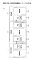
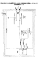
図2は、実施の形態1の抵抗調整回路を含むLSI20A及び20Bの境界の部分を示す図である。LSI20A及び20Bは、例えば、図1に示す演算処理装置11及び制御装置12、又は、制御装置12及び記憶装置13に相当する。
FIG. 2 is a diagram illustrating a boundary portion between the LSIs 20A and 20B including the resistance adjustment circuit according to the first embodiment. The LSIs 20A and 20B correspond to, for example, the arithmetic processing device 11 and the
LSI20A、20Bは、それぞれ、高速シリアルインターフェース50A、50Bを含む。高速シリアルインターフェース50A及び50Bは、例えば、図1に示す高速シリアルインターフェース11B及び12A、又は、高速シリアルインターフェース12C及び13Aに相当する。
The LSIs 20A and 20B include high-speed
ここでは、一例として、LSI20A及び20Bが演算処理装置11及び制御装置12、又は、制御装置12及び記憶装置13に相当し、高速シリアルインターフェース50A及び50Bが、高速シリアルインターフェース11B及び12A、又は、高速シリアルインターフェース12C及び13Aに相当する形態について説明する。
Here, as an example, the LSIs 20A and 20B correspond to the arithmetic processing unit 11 and the
しかしながら、LSI20A及び20Bは、互いの間でデータを伝送する独立したLSIであればよく、図1に示す演算処理装置11及び制御装置12、又は、制御装置12及び記憶装置13に限定されるものではない。
However, the LSIs 20A and 20B may be independent LSIs that transmit data between each other, and are limited to the arithmetic processing unit 11 and the
また、高速シリアルインターフェース50A及び50Bは、高速シリアルインターフェース11B及び12A、又は、高速シリアルインターフェース12C及び13Aに限定されるものではなく、それぞれ、独立したLSIに含まれ、LSI同士の間におけるデータの送信又は受信を行うインターフェースであればよい。
The high-speed
高速シリアルインターフェース50Aと50Bは、伝送線路80で接続されている。伝送線路80は、例えば、LSI20A、20Bが実装されるPCB(Printed Circuit Board)に形成されるバス、又は、LSI20A、20Bを含むパッケージに設けられるバスである。
The high-speed
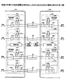
高速シリアルインターフェース50Aは、ドライバ51A1、51A2、調整回路52A、レシーバ53A1、53A2、及びキャパシタ54A1、54A2を含む。
The high-speed
同様に、高速シリアルインターフェース50Bは、ドライバ51B1、51B2、調整回路52B、レシーバ53B1、53B2、及びキャパシタ54B1、54B2を含む。 Similarly, the high-speed serial interface 50B includes drivers 51B1 and 51B2, an adjustment circuit 52B, receivers 53B1 and 53B2, and capacitors 54B1 and 54B2.
実施の形態1の抵抗調整回路は、調整回路52A及び52Bに含まれる。
The resistance adjustment circuit of the first embodiment is included in
高速シリアルインターフェース50A及び50Bは、互いに同様の構成を有するため、ここでは、高速シリアルインターフェース50Aの構成について説明する。
Since the high-speed
ドライバ51A1は、バッファ61A1、及び、終端抵抗部62A1を含む。 The driver 51A1 includes a buffer 61A1 and a termination resistor 62A1.
バッファ61A1には、LSI20Aの内部の処理部から送信データが入力される。送信データは、LSI20AからLSI20Bに送信されるデータである。バッファ61A1は、送信データを差動形式のデータに変換し、一対の伝送線路80を介して、高速シリアルインターフェース50Bのレシーバ53B1に送信データを伝送する。
Transmission data is input to the buffer 61A1 from the processing unit inside the LSI 20A. The transmission data is data transmitted from the LSI 20A to the LSI 20B. The buffer 61A1 converts the transmission data into differential data, and transmits the transmission data to the receiver 53B1 of the high-speed serial interface 50B via the pair of
終端抵抗部62A1は、バッファ61A1と一対の伝送線路80との間から分岐して電源VDDとの間に直列に挿入される一対の可変抵抗器を含む。終端抵抗部62A1は、調整回路52Aから入力される送信調整コードに応じて、一対の可変抵抗器の抵抗値を調整し、バッファ61A1と、一対の伝送線路80との間の伝送路の特性インピーダンスを目標値に設定する。特性インピーダンスの目標値は、典型的には50Ωである。
Termination resistor 62A1 includes a pair of variable resistors that are branched from between buffer 61A1 and the pair of
ドライバ51A2は、バッファ61A2、及び、終端抵抗部62A2を含む。 The driver 51A2 includes a buffer 61A2 and a termination resistor 62A2.
バッファ61A2には、LSI20Aの内部の処理部から送信データが入力される。送信データは、LSI20AからLSI20Bに送信されるデータである。バッファ61A2は、送信データを差動形式のデータに変換し、一対の伝送線路80を介して、高速シリアルインターフェース50Bのレシーバ53B2に送信データを伝送する。
Transmission data is input to the buffer 61A2 from the processing unit inside the LSI 20A. The transmission data is data transmitted from the LSI 20A to the LSI 20B. The buffer 61A2 converts the transmission data into differential data, and transmits the transmission data to the receiver 53B2 of the high-speed serial interface 50B via the pair of
終端抵抗部62A2は、バッファ61A2と一対の伝送線路80との間から分岐して電源VDDとの間に直列に挿入される一対の可変抵抗器を含む。終端抵抗部62A2は、調整回路52Aから入力される送信調整コードに応じて、一対の可変抵抗器の抵抗値を調整し、バッファ61A2と、一対の伝送線路80との間の伝送路の特性インピーダンスを目標値に設定する。特性インピーダンスの目標値は、典型的には50Ωである。
Termination resistor 62A2 includes a pair of variable resistors that are branched from between buffer 61A2 and the pair of
調整回路52Aは、実施の形態1の抵抗調整回路を含み、終端抵抗部62A1、62A2、64A1、64A2にそれぞれ含まれる一対の可変抵抗器の抵抗値を調整する送信調整コード及び受信調整コードを出力する。ドライバ51A1、51A2と、レシーバ53A1、53A2とでは、可変抵抗器の抵抗値の調整度合が異なる場合があるため、調整回路52Aは、終端抵抗部62A1及び62A2と、終端抵抗部64A1及び64A2とに、それぞれ、送信回路用の送信調整コードと、受信回路用の受信調整コードを入力する。
The
なお、調整回路52Aには、基準抵抗器70Aが接続される。実施の形態1の抵抗調整回路は、基準抵抗器70Aに接続される。実施の形態1の抵抗調整回路の詳細については後述する。
A reference resistor 70A is connected to the
レシーバ53A1は、受信回路63A1、及び、終端抵抗部64A1を含む。 The receiver 53A1 includes a reception circuit 63A1 and a termination resistor 64A1.
受信回路63A1の一対の入力端子は、一対のキャパシタ54A1を介して、一対の伝送線路80に接続されている。
The pair of input terminals of the reception circuit 63A1 is connected to the pair of
受信回路63A1は、キャパシタ54A1及び伝送線路80を介してLSI20Bのドライバ51B1からデータを受信する。受信データは、LSI20BからLSI20Aに送信されるデータである。受信回路63A1は、差動形式の受信データをシングルエンド形式のデータに変換し、LSI20Aの内部の処理部に伝送する。
The receiving circuit 63A1 receives data from the driver 51B1 of the LSI 20B via the capacitor 54A1 and the
レシーバ53A1が、キャパシタ54A1を介して伝送線路80に接続されているのは、レシーバ53A1と伝送線路80を交流結合するためである。すなわち、レシーバ53A1は、ドライバ51B1に対して交流的に結合されている。レシーバ53A1は、ドライバ51B1から送信されるデータの交流成分のみを受信する。
The reason why the receiver 53A1 is connected to the
レシーバ53A1がドライバ51B1から受信するデータは、終端抵抗部64A1で所定の直流電圧に重畳される。 Data received by the receiver 53A1 from the driver 51B1 is superimposed on a predetermined DC voltage by the termination resistor 64A1.
終端抵抗部64A1は、受信回路63A1と一対のキャパシタ54A1との間から分岐して電源VDRとの間に直列に挿入される一対の可変抵抗器を含む。終端抵抗部64A1は、調整回路52Aから入力される受信調整コードに応じて、一対の可変抵抗器の抵抗値を調整し、受信回路63A1と、一対の伝送線路80との間のキャパシタ54A1を含む伝送路の特性インピーダンスを目標値に設定する。特性インピーダンスの目標値は、典型的には50Ωである。
Termination resistor unit 64A1 includes a pair of variable resistors that are branched from reception circuit 63A1 and a pair of capacitors 54A1 and inserted in series between power supply VDR. Termination resistor 64A1 adjusts the resistance value of the pair of variable resistors in accordance with the reception adjustment code input from
電源VDRの出力電圧VDRは、レシーバ53A1、53A2、53B1、53B2が最適な動作点(電圧)でデータを受信できる任意の電圧である。レシーバ53A1、53A2、53B1、53B2の最適な動作電圧と、ドライバ51A1、51A2、51B1、51B2の動作電圧(電源電圧VDD)とは異なる。これは、レシーバ53A1、53A2、53B1、53B2の最適な動作点と、ドライバ51A1、51A2、51B1、51B2の最適な動作点とが異なるためである。 The output voltage VDR of the power supply VDR is an arbitrary voltage at which the receivers 53A1, 53A2, 53B1, and 53B2 can receive data at the optimum operating point (voltage). The optimum operating voltage of the receivers 53A1, 53A2, 53B1, and 53B2 is different from the operating voltage (power supply voltage VDD) of the drivers 51A1, 51A2, 51B1, and 51B2. This is because the optimum operating point of the receivers 53A1, 53A2, 53B1, and 53B2 and the optimum operating point of the drivers 51A1, 51A2, 51B1, and 51B2 are different.
レシーバ53A2は、受信回路63A2、及び、終端抵抗部64A2を含む。 The receiver 53A2 includes a reception circuit 63A2 and a termination resistance unit 64A2.
受信回路63A2の一対の入力端子は、一対のキャパシタ54A2を介して、一対の伝送線路80に接続されている。
The pair of input terminals of the receiving circuit 63A2 is connected to the pair of
受信回路63A2は、キャパシタ54A2及び伝送線路80を介してLSI20Bのドライバ51B2からデータを受信する。受信データは、LSI20BからLSI20Aに送信されるデータである。受信回路63A2は、差動形式の受信データをシングルエンド形式のデータに変換し、LSI20Aの内部の処理部に伝送する。
The receiving circuit 63A2 receives data from the driver 51B2 of the LSI 20B via the capacitor 54A2 and the
レシーバ53A2が、キャパシタ54A2を介して伝送線路80に接続されているのは、レシーバ53A2と伝送線路80を交流結合するためである。すなわち、レシーバ53A2は、ドライバ51B2に対して交流的に結合されている。レシーバ53A2は、ドライバ51B2から送信されるデータの交流成分のみを受信する。
The reason why the receiver 53A2 is connected to the
レシーバ53A2がドライバ51B2から受信するデータは、終端抵抗部64A2で所定の直流電圧に重畳される。 Data received by the receiver 53A2 from the driver 51B2 is superimposed on a predetermined DC voltage by the termination resistor 64A2.
終端抵抗部64A2は、受信回路63A2と一対のキャパシタ54A2との間から分岐して電源VDRとの間に直列に挿入される一対の可変抵抗器を含む。終端抵抗部64A2は、調整回路52Aから入力される受信調整コードに応じて、一対の可変抵抗器の抵抗値を調整し、受信回路63A2と、一対の伝送線路80との間のキャパシタ54A2を含む伝送路の特性インピーダンスを目標値に設定する。特性インピーダンスの目標値は、典型的には50Ωである。
Termination resistor unit 64A2 includes a pair of variable resistors that are branched from between receiving circuit 63A2 and a pair of capacitors 54A2 and inserted in series between power supply VDR. Termination resistor 64A2 adjusts the resistance value of the pair of variable resistors in accordance with the reception adjustment code input from
一対のキャパシタ54A1は、レシーバ53A1の受信回路63A1の一対の入力端子と、一対の伝送線路80との間に、それぞれ直列に挿入されている。キャパシタ54A1は、受信回路63A1と伝送線路80を交流的に結合している。すなわち、キャパシタ54A1は、レシーバ53A1とドライバ51B1を交流的に結合している。キャパシタ54A1は、ドライバ51B1から送信されるデータの交流成分のみをレシーバ53A1に伝送する。
The pair of capacitors 54A1 are inserted in series between the pair of input terminals of the reception circuit 63A1 of the receiver 53A1 and the pair of
一対のキャパシタ54A2は、レシーバ53A2の受信回路63A2の一対の入力端子と、一対の伝送線路80との間に、それぞれ直列に挿入されている。キャパシタ54A2は、受信回路63A2と伝送線路80を交流的に結合している。すなわち、キャパシタ54A2は、レシーバ53A2とドライバ51B2を交流的に結合している。キャパシタ54A2は、ドライバ51B2から送信されるデータの交流成分のみをレシーバ53A2に伝送する。
The pair of capacitors 54A2 are inserted in series between the pair of input terminals of the reception circuit 63A2 of the receiver 53A2 and the pair of
また、高速シリアルインターフェース50Bのドライバ51B1、51B2、調整回路52B、レシーバ53B1、53B2、及びキャパシタ54B1、54B2については、次の通りである。 The drivers 51B1 and 51B2, the adjustment circuit 52B, the receivers 53B1 and 53B2, and the capacitors 54B1 and 54B2 of the high-speed serial interface 50B are as follows.
ドライバ51B1は、バッファ61B1、及び、終端抵抗部62B1を含む。 The driver 51B1 includes a buffer 61B1 and a termination resistor 62B1.
ドライバ51B2、バッファ61B2、及び、終端抵抗部62B2を含む。 A driver 51B2, a buffer 61B2, and a termination resistor 62B2 are included.
調整回路52Bは、実施の形態1の抵抗調整回路を含み、終端抵抗部62B1、62B2、64A1、64A2に送信調整コード及び受信調整コードを出力する。調整回路52Aには、基準抵抗器70Bが接続される。実施の形態1の抵抗調整回路は、基準抵抗器70Bに接続される。実施の形態1の抵抗調整回路の詳細については後述する。
The adjustment circuit 52B includes the resistance adjustment circuit of the first embodiment, and outputs a transmission adjustment code and a reception adjustment code to the termination resistor units 62B1, 62B2, 64A1, and 64A2. A reference resistor 70B is connected to the
レシーバ53B1は、受信回路63B1、及び、終端抵抗部64B1を含む。 The receiver 53B1 includes a reception circuit 63B1 and a termination resistor 64B1.
レシーバ53B2は、受信回路63B2、及び、終端抵抗部64B2を含む。 The receiver 53B2 includes a reception circuit 63B2 and a termination resistor 64B2.
一対のキャパシタ54B1は、レシーバ53B1の受信回路63B1の一対の入力端子と、一対の伝送線路80との間に、それぞれ直列に挿入されている。
The pair of capacitors 54B1 are inserted in series between the pair of input terminals of the reception circuit 63B1 of the receiver 53B1 and the pair of
一対のキャパシタ54B2は、レシーバ53B2の受信回路63B2の一対の入力端子と、一対の伝送線路80との間に、それぞれ直列に挿入されている。
The pair of capacitors 54B2 are inserted in series between the pair of input terminals of the reception circuit 63B2 of the receiver 53B2 and the pair of
高速シリアルインターフェース50Bのドライバ51B1、51B2、調整回路52B、レシーバ53B1、53B2、及びキャパシタ54B1、54B2の回路構成は、高速シリアルインターフェース50Aのドライバ51A1、51A2、調整回路52A、レシーバ53A1、53A2、及びキャパシタ54A1、54A2の回路構成と同様である。
The circuit configurations of the drivers 51B1 and 51B2, the adjustment circuit 52B, the receivers 53B1 and 53B2, and the capacitors 54B1 and 54B2 of the high-speed serial interface 50B are the same as the drivers 51A1 and 51A2, the
ドライバ51B1、51B2、調整回路52B、レシーバ53B1、53B2、及びキャパシタ54B1、54B2の回路構成は、ドライバ51A1、51A2、調整回路52A、レシーバ53A1、53A2、及びキャパシタ54A1、54A2の添え字AをBに置き換えたものである。
The circuit configurations of the drivers 51B1 and 51B2, the adjustment circuit 52B, the receivers 53B1 and 53B2, and the capacitors 54B1 and 54B2 are changed from B to the subscript A of the drivers 51A1 and 51A2, the
このため、高速シリアルインターフェース50Bのドライバ51B1、51B2、調整回路52B、レシーバ53B1、53B2、及びキャパシタ54B1、54B2の回路構成の説明は省略する。 Therefore, the description of the circuit configurations of the drivers 51B1 and 51B2, the adjustment circuit 52B, the receivers 53B1 and 53B2, and the capacitors 54B1 and 54B2 of the high-speed serial interface 50B is omitted.
上述のような高速シリアルインターフェース50A、50Bは、それぞれ、調整回路52A及び52Bを1つずつ含む。
Each of the high-speed
調整回路52Aは、送信用の終端抵抗部62A1、62A2と同様の送信用の終端抵抗部を内部に含み、内部の送信用の終端抵抗部の抵抗値を調整する送信調整コードを送信用の終端抵抗部62A1、62A2に分配する。
The
また、調整回路52Aは、受信用の終端抵抗部64A1、64A2と同様の受信用の終端抵抗部を内部に含み、内部の受信用の終端抵抗部の抵抗値を調整する受信調整コードを受信用の終端抵抗部64A1、64A2に分配する。
The
同様に、調整回路52Bは、送信用の終端抵抗部62B1、62B2と同様の送信用の終端抵抗部と、受信用の終端抵抗部64A1、64A2と同様の受信用の終端抵抗部とを内部に含む。調整回路52Bは、内部の送信用及び受信用の終端抵抗部の抵抗値を調整する送信調整コード及び受信調整コードを、それぞれ、送信用の終端抵抗部62A1、62A2と受信用の終端抵抗部64A1、64A2とに分配する。 Similarly, the adjustment circuit 52B includes a transmission termination resistor unit similar to the transmission termination resistor units 62B1 and 62B2 and a reception termination resistor unit similar to the reception termination resistor units 64A1 and 64A2. Including. The adjustment circuit 52B includes transmission adjustment codes and reception adjustment codes for adjusting the resistance values of the internal transmission and reception termination resistor units, respectively, the transmission termination resistor units 62A1 and 62A2, and the reception termination resistor unit 64A1. , 64A2.
また、上述のような高速シリアルインターフェース50A、50Bは、キャパシタ54A1、54A2、54B1、54B2を用いて、レシーバ53A1、53A2、53B1、53B2を伝送線路80に交流的に結合している。
In the high-speed
高速シリアルインターフェース50A、50Bでは、送信側のLSI20Aと受信側のLSI20Bの電源電圧VDDの差を吸収するため、又は、レシーバ53A1、53A2、53B1、53B2が最適な動作点(電圧)で動作してデータを受信できるようにするために、交流結合形式でデータを受信するようにしている。このために、レシーバ53A1、53A2、53B1、53B2と伝送線路80との間に、キャパシタ54A1、54A2、54B1、54B2を設けている。
In the high-speed
なお、図2には、キャパシタ54A1及び54A2がLSI20Aの一部であり、キャパシタ54B1及び54B2がLSI20Bの一部である形態を示すが、キャパシタ54A1、54A2、54B1、54B2は、LSI20A及び20Bの外部に配設されていてもよい。例えば、キャパシタ54A1、54A2、54B1、54B2は、LSI20A及び20Bが実装されるPCBに実装されるキャパシタチップであってもよい。 FIG. 2 shows a configuration in which the capacitors 54A1 and 54A2 are part of the LSI 20A and the capacitors 54B1 and 54B2 are part of the LSI 20B. However, the capacitors 54A1, 54A2, 54B1, and 54B2 are external to the LSIs 20A and 20B. It may be arranged. For example, the capacitors 54A1, 54A2, 54B1, and 54B2 may be capacitor chips mounted on a PCB on which the LSIs 20A and 20B are mounted.
このような交流結合形式の伝送方式を採用した場合、レシーバ53A1、53A2、53B1、53B2の終端抵抗部64A1、64A2、64B1、64B2の終端電圧は、レシーバ53A1、53A2、53B1、53B2が最適な動作点(電圧)でデータを受信できる任意の電圧VDRに設定されている。 When such an AC coupling type transmission method is adopted, the terminating voltages of the terminating resistors 64A1, 64A2, 64B1, and 64B2 of the receivers 53A1, 53A2, 53B1, and 53B2 are optimal for the receivers 53A1, 53A2, 53B1, and 53B2. An arbitrary voltage VDR that can receive data at a point (voltage) is set.
レシーバ53A1、53A2、53B1、53B2の終端電圧VDRは、ドライバ51A1、51A2、51B1、51B2の電源電圧VDDとは異なる。 The termination voltage VDR of the receivers 53A1, 53A2, 53B1, and 53B2 is different from the power supply voltage VDD of the drivers 51A1, 51A2, 51B1, and 51B2.
終端抵抗部64A1、64A2、64B1、64B2は、例えば、並列接続される複数の抵抗器と、各抵抗器に直列に接続されるトランジスタとを含み、トランジスタのオン/オフを切り替えて並列接続される抵抗器の数を変えることにより、合成抵抗値を変化させる可変抵抗器である。 The termination resistor units 64A1, 64A2, 64B1, and 64B2 include, for example, a plurality of resistors connected in parallel and transistors connected in series to the resistors, and are connected in parallel by switching on / off of the transistors. It is a variable resistor that changes the combined resistance value by changing the number of resistors.
終端抵抗部64A1、64A2、64B1、64B2には、内部のトランジスタが抵抗値ゼロの理想的なスイッチのように振る舞い、抵抗器のみで合成抵抗値が決まることが求められる。 The terminating resistor portions 64A1, 64A2, 64B1, and 64B2 are required to have an internal transistor behave like an ideal switch having a resistance value of zero and determine a combined resistance value only by a resistor.
しかしながら、トランジスタを抵抗値ゼロのスイッチのように振る舞わせるためには、トランジスタのサイズを大きくする必要がある。その場合、トランジスタのドレイン容量が大きくなってしまい、伝送経路の容量が増えることによって信号の伝送品質が劣化する。 However, in order for a transistor to behave like a switch having a zero resistance value, it is necessary to increase the size of the transistor. In that case, the drain capacity of the transistor increases, and the transmission quality of the signal deteriorates due to an increase in the capacity of the transmission path.
このため、トランジスタのサイズをある程度小さくして信号の伝送品質を確保した状態で、トランジスタを抵抗器の一部として利用することになる。この場合、トランジスタは、ドレイン電圧とソース電圧に依存して抵抗値が変化する素子になる。 For this reason, the transistor is used as a part of the resistor in a state in which the size of the transistor is reduced to some extent to ensure signal transmission quality. In this case, the transistor is an element whose resistance value changes depending on the drain voltage and the source voltage.
従って、終端抵抗部64A1、64A2、64B1、64B2の各々の抵抗値は、伝送信号の信号レベル又は終端電圧VDRに対して依存性を持つことになる。 Accordingly, the resistance values of the termination resistor units 64A1, 64A2, 64B1, and 64B2 have dependency on the signal level of the transmission signal or the termination voltage VDR.
以上のような理由から、図2に示す高速シリアルインターフェース50A、50Bでは、特に、レシーバ53A1、53A2、53B1、53B2の終端抵抗部64A1、64A2、64B1、64B2の抵抗値を終端電圧VDRに応じて高精度に設定することが必要になる。
For the reasons described above, in the high-speed
次に、終端抵抗部62A1、62A2、64A1、64A2、62B1、62B2、64B1、64B2の構成について説明する
図3は、実施の形態1の終端抵抗部90A、90Bの回路構成を示す図である。
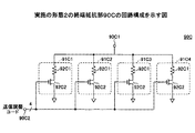
Next, the configuration of the termination resistor units 62A1, 62A2, 64A1, 64A2, 62B1, 62B2, 64B1, and 64B2 will be described. FIG. 3 is a diagram illustrating a circuit configuration of the
図2に示すドライバ51A1、51A2、51B1、51B2にそれぞれ含まれる送信側の終端抵抗部62A1、62A2、62B1、62B2の一対の可変抵抗器は、図3(A)に示す終端抵抗部90Aの回路構成を有する。
A pair of variable resistors of transmission-side termination resistor units 62A1, 62A2, 62B1, and 62B2 included in the drivers 51A1, 51A2, 51B1, and 51B2 shown in FIG. 2 are the circuits of the
また、図2に示すレシーバ53A1、53A2、53B1、53B2にそれぞれ含まれる受信側の終端抵抗部64A1、64A2、64B1、64B2の一対の可変抵抗器は、図3(B)に示す終端抵抗部90Bの回路構成を有する。 A pair of variable resistors on the receiving side 64A1, 64A2, 64B1, 64B2 included in each of the receivers 53A1, 53A2, 53B1, and 53B2 shown in FIG. 2 is a terminating resistor 90B shown in FIG. 3B. The circuit configuration is as follows.
図3(A)に示す終端抵抗部90Aは、端子90A1、90A2、及び、調整部91A1、91A2、91A3、91A4を含む。なお、端子90A2は、4つの調整部91A1、91A2、91A3、91A4に対応して4つ設けられている。 3A includes terminals 90A1 and 90A2 and adjustment units 91A1, 91A2, 91A3, and 91A4. In addition, four terminals 90A2 are provided corresponding to the four adjustment units 91A1, 91A2, 91A3, and 91A4.
端子90A1は、電源電圧VDDと、調整部91A1、91A2、91A3、91A4の合成抵抗値とを反映した信号を出力する端子である。端子90A1は、図2に示すドライバ51A1、51A2、51B1、51B2にそれぞれ含まれる送信側の終端抵抗部62A1、62A2、62B1、62B2の一対の可変抵抗器の下側の端子に相当する。 The terminal 90A1 is a terminal that outputs a signal reflecting the power supply voltage VDD and the combined resistance values of the adjustment units 91A1, 91A2, 91A3, and 91A4. The terminal 90A1 corresponds to the lower terminal of the pair of variable resistors of the transmission-side termination resistor units 62A1, 62A2, 62B1, and 62B2 included in the drivers 51A1, 51A2, 51B1, and 51B2 shown in FIG.
端子90A2は、送信調整コードが入力される端子であり、図2に示すドライバ51A1、51A2、51B1、51B2にそれぞれ含まれる送信側の終端抵抗部62A1、62A2、62B1、62B2に送信調整コードが入力される端子に相当する。 The terminal 90A2 is a terminal to which a transmission adjustment code is input, and the transmission adjustment code is input to the transmission-side termination resistor units 62A1, 62A2, 62B1, and 62B2 included in the drivers 51A1, 51A2, 51B1, and 51B2 shown in FIG. This corresponds to the terminal to be used.
調整部91A1、91A2、91A3、91A4は、同様の構成を有する。 The adjustment units 91A1, 91A2, 91A3, 91A4 have the same configuration.
調整部91A1は、抵抗器92A1、PMOS(P channel Metal Oxide Semiconductor)トランジスタ92A2、及びインバータ92A3を含む。 The adjustment unit 91A1 includes a resistor 92A1, a PMOS (P channel Metal Oxide Semiconductor) transistor 92A2, and an inverter 92A3.
抵抗器92A1は、端子90A1と、PMOSトランジスタ92A2のドレインとの間に接続される。 The resistor 92A1 is connected between the terminal 90A1 and the drain of the PMOS transistor 92A2.
PMOSトランジスタ92A2は、ドレインが抵抗器92A1に接続され、ゲートがインバータ92A3の出力端子に接続され、ソースが電源VDDに接続される。 The PMOS transistor 92A2 has a drain connected to the resistor 92A1, a gate connected to the output terminal of the inverter 92A3, and a source connected to the power supply VDD.
インバータ92A3は、入力端子が端子90A2に接続され、出力端子がPMOSトランジスタ92A2のゲートに接続される。 The inverter 92A3 has an input terminal connected to the terminal 90A2 and an output terminal connected to the gate of the PMOS transistor 92A2.
調整部91A2、91A3、91A4は、調整部91A1と同様の構成を有する。調整部91A1、91A2、91A3、91A4の抵抗器92A1は、端子90A1に対して並列に接続され、調整部91A1、91A2、91A3、91A4のインバータ92A3の入力端子は、それぞれ、4つの端子90A2に接続される。 The adjustment units 91A2, 91A3, 91A4 have the same configuration as the adjustment unit 91A1. The resistors 92A1 of the adjustment units 91A1, 91A2, 91A3, and 91A4 are connected in parallel to the terminal 90A1, and the input terminals of the inverters 92A3 of the adjustment units 91A1, 91A2, 91A3, and 91A4 are connected to the four terminals 90A2, respectively. Is done.
終端抵抗部90Aは、4つの端子90A2に入力される送信調整コードによって、調整部91A1、91A2、91A3、91A4のPMOSトランジスタ92A2のオン/オフが調整される。
In the terminating
PMOSトランジスタ92A2がオンにされる調整部(91A1、91A2、91A3、91A4)の数が増えると、並列に接続される抵抗器92A1の数が増えるため、終端抵抗部90Aの合成抵抗値は低下する。
When the number of adjustment units (91A1, 91A2, 91A3, 91A4) in which the PMOS transistor 92A2 is turned on increases, the number of resistors 92A1 connected in parallel increases, so the combined resistance value of the
PMOSトランジスタ92A2がオンにされる調整部(91A1、91A2、91A3、91A4)の数が少なくなると、並列に接続される抵抗器92A1の数が減るため、終端抵抗部90Aの合成抵抗値は増大する。
When the number of adjustment units (91A1, 91A2, 91A3, 91A4) in which the PMOS transistor 92A2 is turned on decreases, the number of resistors 92A1 connected in parallel decreases, so that the combined resistance value of the
調整部91A1,91A2、91A3、91A4の各抵抗値と各トランジスタのサイズは、合成抵抗値が短調増減するように設計されていればよい。また、調整部の数はプロセスばらつきの調整範囲を確保するために調整部の数を増減してもよい。 The resistance values of the adjustment units 91A1, 91A2, 91A3, and 91A4 and the sizes of the transistors only have to be designed so that the combined resistance value is increased or decreased in minor. Further, the number of adjustment units may be increased or decreased in order to secure an adjustment range of process variation.
図3(B)に示す終端抵抗部90Bは、端子90B1、90B2、90B3、及び、調整部91B1、91B2、91B3、91B4を含む。なお、端子90B2は、4つの調整部91B1、91B2、91B3、91B4に対応して4つ設けられている。 3B includes terminals 90B1, 90B2, 90B3, and adjustment units 91B1, 91B2, 91B3, 91B4. In addition, four terminals 90B2 are provided corresponding to the four adjustment units 91B1, 91B2, 91B3, and 91B4.
端子90B1は、終端電圧VDRと、調整部91B1、91B2、91B3、91B4の合成抵抗値とを反映した信号(電圧)を出力する端子である。端子90B1は、図2に示すレシーバ53A1、53A2、53B1、53B2にそれぞれ含まれる受信側の終端抵抗部64A1、64A2、64B1、64B2の一対の可変抵抗器の下側の端子に相当する。 The terminal 90B1 is a terminal that outputs a signal (voltage) reflecting the termination voltage VDR and the combined resistance value of the adjusting units 91B1, 91B2, 91B3, and 91B4. The terminal 90B1 corresponds to the lower terminal of the pair of variable resistors of the receiving-side termination resistor parts 64A1, 64A2, 64B1, and 64B2 included in the receivers 53A1, 53A2, 53B1, and 53B2 shown in FIG.
端子90B2は、受信調整コードが入力される端子であり、図2に示すレシーバ53A1、53A2、53B1、53B2にそれぞれ含まれる受信側の終端抵抗部64A1、64A2、64B1、64B2に受信調整コードが入力される端子に相当する。 The terminal 90B2 is a terminal to which a reception adjustment code is input, and the reception adjustment code is input to the reception-side termination resistor sections 64A1, 64A2, 64B1, and 64B2 included in the receivers 53A1, 53A2, 53B1, and 53B2 illustrated in FIG. This corresponds to the terminal to be used.
端子90B3は、終端電圧VDRが入力される端子である。 The terminal 90B3 is a terminal to which the termination voltage VDR is input.
調整部91B1、91B2、91B3、91B4は、同様の構成を有する。 The adjustment units 91B1, 91B2, 91B3, 91B4 have the same configuration.
調整部91B1は、抵抗器92B1、PMOSトランジスタ92B2、NMOS(N channel Metal Oxide Semiconductor)トランジスタ92B3、及びインバータ92B4を含む。 The adjustment unit 91B1 includes a resistor 92B1, a PMOS transistor 92B2, an NMOS (N channel Metal Oxide Semiconductor) transistor 92B3, and an inverter 92B4.
抵抗器92B1は、端子90B1と、PMOSトランジスタ92B2のドレイン、及び、NMOSトランジスタ92B3のソースとの間に接続される。 The resistor 92B1 is connected between the terminal 90B1, the drain of the PMOS transistor 92B2, and the source of the NMOS transistor 92B3.
PMOSトランジスタ92B2は、ドレインが抵抗器92B1と、NMOSトランジスタ92B3のソースとに接続され、ゲートがインバータ92B3の出力端子に接続され、ソースが端子90B3に接続される。 The PMOS transistor 92B2 has a drain connected to the resistor 92B1 and the source of the NMOS transistor 92B3, a gate connected to the output terminal of the inverter 92B3, and a source connected to the terminal 90B3.
NMOSトランジスタ92B3は、ソースが抵抗器92B1と、PMOSトランジスタ92B2のドレインとに接続され、ゲートが端子90B2に接続され、ソースが端子90B3に接続される。 The NMOS transistor 92B3 has a source connected to the resistor 92B1 and the drain of the PMOS transistor 92B2, a gate connected to the terminal 90B2, and a source connected to the terminal 90B3.
インバータ92B4は、入力端子が端子90B2に接続され、出力端子がPMOSトランジスタ92B2のゲートに接続される。 The inverter 92B4 has an input terminal connected to the terminal 90B2, and an output terminal connected to the gate of the PMOS transistor 92B2.
調整部91B2、91B3、91B4は、調整部91B1と同様の構成を有する。調整部91B1、91B2、91B3、91B4の抵抗器92B1は、端子90B1に対して並列に接続され、調整部91B1、91B2、91B3、91B4のインバータ92B4の入力端子は、それぞれ、4つの端子90B2に接続される。 The adjustment units 91B2, 91B3, 91B4 have the same configuration as the adjustment unit 91B1. The resistors 92B1 of the adjustment units 91B1, 91B2, 91B3, and 91B4 are connected in parallel to the terminal 90B1, and the input terminals of the inverters 92B4 of the adjustment units 91B1, 91B2, 91B3, and 91B4 are connected to the four terminals 90B2, respectively. Is done.
終端抵抗部90Bは、4つの端子90B2に入力される受信調整コードによって、調整部91B1、91B2、91B3、91B4のPMOSトランジスタ92B2及びNMOSトランジスタ92B3のオン/オフが調整される。 In the termination resistor 90B, on / off of the PMOS transistor 92B2 and the NMOS transistor 92B3 of the adjustment units 91B1, 91B2, 91B3, and 91B4 is adjusted by the reception adjustment code input to the four terminals 90B2.
PMOSトランジスタ92B2及びNMOSトランジスタ92B3がオンにされる調整部(91B1、91B2、91B3、91B4)の数が増えると、並列に接続される抵抗器92B1の数が増えるため、終端抵抗部90Bの合成抵抗値は低下する。 When the number of adjustment units (91B1, 91B2, 91B3, 91B4) in which the PMOS transistor 92B2 and the NMOS transistor 92B3 are turned on increases, the number of resistors 92B1 connected in parallel increases, so that the combined resistance of the termination resistor unit 90B The value drops.
PMOSトランジスタ92B2及びNMOSトランジスタ92B3がオンにされる調整部(91B1、91B2、91B3、91B4)の数が少なくなると、並列に接続される抵抗器92B1の数が減るため、終端抵抗部90Bの合成抵抗値は増大する。 When the number of adjustment units (91B1, 91B2, 91B3, 91B4) in which the PMOS transistor 92B2 and the NMOS transistor 92B3 are turned on decreases, the number of resistors 92B1 connected in parallel decreases, so that the combined resistance of the termination resistor unit 90B The value increases.
調整部91B1、91B2、91B3、91B4の各抵抗値と各トランジスタのサイズは、合成抵抗値が短調増減するように設計されていればよい。 The resistance values of the adjustment units 91B1, 91B2, 91B3, and 91B4 and the sizes of the transistors only have to be designed so that the combined resistance value is increased or decreased in minor.
また、調整部の数はプロセスばらつきの調整範囲を確保するために調整部の数を増減してもよい。 次に、図4を用いて、図3(B)に示す終端抵抗部90Bの合成抵抗値(終端抵抗値)の終端電圧VDRと信号電圧に対する依存性について説明する。 Further, the number of adjustment units may be increased or decreased in order to secure an adjustment range of process variation. Next, the dependency of the combined resistance value (termination resistance value) of the termination resistance unit 90B shown in FIG. 3B on the termination voltage VDR and the signal voltage will be described with reference to FIG.
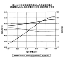
図4は、図3(B)に示す終端抵抗部90Bの終端抵抗値の終端電圧VDRと信号電圧に対する依存性を示す図である。 FIG. 4 is a diagram illustrating the dependency of the termination resistance value of the termination resistor unit 90B illustrated in FIG. 3B on the termination voltage VDR and the signal voltage.
図4には、終端電圧VDRが0V(VSS:接地電圧)の場合に設定される受信調整コードを用いて、終端電圧VDRをVSSに設定した状態で終端抵抗部90Aが動作した場合の端子間電圧に対する終端抵抗値の特性を実線で示す。端子間電圧とは、終端抵抗部90Bの端子90B1と端子90B3(図3(B)参照)との間に生じる電圧である。
FIG. 4 shows the connection between terminals when the
また、図4には、終端電圧VDRがVSSの場合に設定される受信調整コードで、終端電圧VDRが600mVをVSSに設定した状態で終端抵抗部90Bが動作した場合の端子間電圧に対する終端抵抗値の特性を細破線で示し、実線の特性と細破線の特性との抵抗値の差分を破線で示す。 Also, FIG. 4 shows a reception adjustment code that is set when the termination voltage VDR is VSS, and the termination resistance with respect to the voltage between the terminals when the termination resistor unit 90B operates in a state where the termination voltage VDR is set to 600 mV as VSS. The characteristic of the value is indicated by a thin broken line, and the difference in resistance value between the characteristic of the solid line and the characteristic of the fine broken line is indicated by a broken line.
なお、実線の特性と細破線の特性の抵抗値は左側の縦軸に示し、実線の特性と細破線の特性との抵抗値の差分は右側の縦軸に示す。横軸は終端抵抗部90Bの端子90B1と端子90B3(図3(B)参照)との間に生じる端子間電圧を示す。 The resistance values of the solid line characteristic and the thin broken line characteristic are shown on the left vertical axis, and the resistance value difference between the solid line characteristic and the thin broken line characteristic is shown on the right vertical axis. The horizontal axis represents the inter-terminal voltage generated between the terminal 90B1 and the terminal 90B3 (see FIG. 3B) of the termination resistor 90B.
図4に実線で示すように、終端電圧VDRがVSSの場合に設定される受信調整コードで与えられる終端抵抗値は、端子間電圧が0.4Vのときに50Ωになるように設定されたとする。これは、終端抵抗部90Aの動作点において、端子間電圧が0.4Vになると想定して、終端抵抗値が50Ωになるように受信調整コードが設定されている場合に相当する。
As shown by the solid line in FIG. 4, it is assumed that the termination resistance value given by the reception adjustment code set when the termination voltage VDR is VSS is set to be 50Ω when the terminal voltage is 0.4V. . This corresponds to the case where the reception adjustment code is set so that the terminal resistance value is 50Ω assuming that the voltage between terminals is 0.4 V at the operating point of the
このように、終端電圧VDRがVSSの場合に設定される受信調整コードを用いて、終端電圧VDRが600mVの環境で終端抵抗部90Aを使用すると、図4に示す実線の特性と細破線の特性とを比べて分かるように、終端抵抗値が50Ωからずれることになる。
As described above, when the
例えば、終端電圧VDRが600mVの場合に端子間電圧が0.6Vになると、終端電圧VDRがVSSの場合に比べて、終端抵抗値が約8Ω小さくなるため、終端抵抗部90Bで受信データの反射等が生じ、信号の伝送特性が劣化するおそれがある。 For example, when the terminal voltage VDR is 600 mV and the terminal voltage is 0.6 V, the terminal resistance value is reduced by about 8Ω compared to the case where the terminal voltage VDR is VSS. Or the like, and there is a risk that the signal transmission characteristics may deteriorate.
終端抵抗部90Aは、伝送経路の容量が増えることによる信号の伝送品質の劣化を抑制するために、トランジスタのサイズが限られているため、図4に示すように終端電圧と端子間電圧に対する依存性を有する。
Since the
このため、終端抵抗部90Bの抵抗値を終端電圧VDRに応じて高精度に設定することが必要になる。 For this reason, it is necessary to set the resistance value of the termination resistor 90B with high accuracy according to the termination voltage VDR.
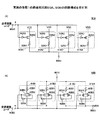
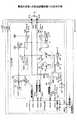
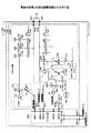
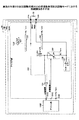
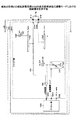
次に、図5を用いて、実施の形態1の抵抗調整回路100について説明する。 Next, the resistance adjustment circuit 100 according to the first embodiment will be described with reference to FIG.
図5は、実施の形態1の抵抗調整回路100を示す図である。 FIG. 5 is a diagram illustrating the resistance adjustment circuit 100 according to the first embodiment.
抵抗調整回路100は、アナログ部100A、デジタル部100D、及び端子100T1、100T2を含む。アナログ部100Aは、高速/高精度なCMOS回路によって構築される。デジタル部100Dは、高速動作が可能なデジタル回路によって構築される。抵抗調整回路100は、図2に示す調整回路52A及び52Bに1つずつ含まれる。
The resistance adjustment circuit 100 includes an analog unit 100A, a digital unit 100D, and terminals 100T1 and 100T2. The analog unit 100A is constructed by a high-speed / high-precision CMOS circuit. The digital unit 100D is constructed by a digital circuit capable of high-speed operation. One resistance adjustment circuit 100 is included in each of the
図5では、抵抗調整回路100がLSI20の高速シリアルインターフェース50に含まれるものとして説明する。LSI20は、図2に示すLSI20A又は20Bに相当する。高速シリアルインターフェース50は、図2に示す高速シリアルインターフェース50A又は50Bに相当する。
In FIG. 5, the resistance adjustment circuit 100 is described as being included in the high-speed
また、抵抗調整回路100には、基準抵抗器70が接続されている。基準抵抗器70は、図2に示す基準抵抗器70A又は70Bに相当する。ここでは、基準抵抗器70の抵抗値Rrefが1kΩである場合について説明する。
A
なお、ここでは、基準抵抗器70は、LSI20の外部に設けられていて、抵抗調整回路100に接続されているものとして説明するが、基準抵抗器70は、抵抗調整回路100の構成要素に含まれていてもよい。
Here, the
抵抗調整回路100のアナログ部100Aは、端子101A、101B、101C、101D、101E、102A、102B、基準電流生成回路110、定電流源120、121、122、123、124、及びセレクタ130、140を含む。
The analog unit 100A of the resistance adjustment circuit 100 includes
抵抗調整回路100のアナログ部100Aは、さらに、電圧バッファ150、終端抵抗部160、170、セレクタ180A、180B、及びコンパレータ190を含む。
The analog unit 100A of the resistance adjustment circuit 100 further includes a
デジタル部100Dは、端子100D1、100D2、100D3、100D4、100D5、100D6、100D7を含む。端子100D1、100D2、100D3、100D4、100D5は、それぞれ、アナログ部100Aの端子101A、101B、101C、101D、101Eに接続されている。デジタル部100Dは、制御部の一例である。
The digital unit 100D includes terminals 100D1, 100D2, 100D3, 100D4, 100D5, 100D6, and 100D7. The terminals 100D1, 100D2, 100D3, 100D4, and 100D5 are connected to the
端子100D1、100D2、100D3、100D5は、それぞれ、電流調整コード、受信調整コード、送信調整コード、選択信号(Iref, Rx Term or Tx Term)を出力する端子である。また、端子100D4は、アナログ部100Aから比較結果が入力される端子である。 Terminals 100D1, 100D2, 100D3, and 100D5 are terminals that output a current adjustment code, a reception adjustment code, a transmission adjustment code, and a selection signal (Iref, Rx Term or Tx Term), respectively. The terminal 100D4 is a terminal to which a comparison result is input from the analog unit 100A.
デジタル部100Dの端子100D6、100D7は、それぞれ、受信調整コード、送信調整コードを抵抗調整回路100の外部に出力するための端子である。端子100D6、100D7は、それぞれ、抵抗調整回路100の端子100T1、100T2に接続されている。 Terminals 100D6 and 100D7 of the digital unit 100D are terminals for outputting the reception adjustment code and the transmission adjustment code to the outside of the resistance adjustment circuit 100, respectively. The terminals 100D6 and 100D7 are connected to the terminals 100T1 and 100T2 of the resistance adjustment circuit 100, respectively.
端子100T1、100T2は、図2に示す調整回路52A及び52Bから受信調整コード及び送信調整コードが出力される端子に相当する。
Terminals 100T1 and 100T2 correspond to terminals from which reception adjustment codes and transmission adjustment codes are output from
端子101A、101B、101C、101D、101Eは、デジタル部100Dに接続される端子である。
端子101Aは、デジタル部100Dから電流調整コードが入力される端子である。端子101Aは、基準電流生成回路110の可変抵抗器112のコード入力端子に接続されている。デジタル部100Dは、端子101Aを介して、可変抵抗器112に電流調整コードを入力する。電流調整コードは、基準電流生成回路110の出力電流値を調整するコードである。
The terminal 101A is a terminal to which a current adjustment code is input from the digital unit 100D. The terminal 101A is connected to the code input terminal of the
端子101Bは、デジタル部100Dから受信調整コードが入力される端子である。端子101Bは、終端抵抗部160のコード入力端子に接続されている。デジタル部100Dは、端子101Bを介して、終端抵抗部160に受信調整コードを入力する。受信調整コードは、終端抵抗部160の終端抵抗値を調整するコードである。
The terminal 101B is a terminal to which a reception adjustment code is input from the digital unit 100D. The terminal 101B is connected to the code input terminal of the
端子101Cは、デジタル部100Dから送信調整コードが入力される端子である。端子101Cは、終端抵抗部170のコード入力端子に接続されている。デジタル部100Dは、端子101Cを介して、終端抵抗部170に送信調整コードを入力する。送信調整コードは、終端抵抗部170の終端抵抗値を調整するコードである。
The terminal 101C is a terminal to which a transmission adjustment code is input from the digital unit 100D. The terminal 101C is connected to the code input terminal of the
端子101Dは、デジタル部100Dにコンパレータ190の比較結果を表す信号を出力する端子である。端子101Dは、コンパレータ190の出力端子に接続されている。コンパレータ190の比較結果を表す信号は、端子101Dを介して、デジタル部100Dに出力される。
The terminal 101D is a terminal that outputs a signal representing the comparison result of the
端子101Eは、デジタル部100Dから選択信号(Iref, Rx Term or Tx Term)が入力される端子である。端子101Eは、セレクタ130、140、180A、180Bの選択信号入力端子に接続されている。デジタル部100Dは、端子101Eを介して、選択信号(Iref, Rx Term or Tx Term)をセレクタ130、140、180A、180Bの選択信号入力端子に入力する。
The terminal 101E is a terminal to which a selection signal (Iref, Rx Term or Tx Term) is input from the digital unit 100D. The
なお、選択信号(Iref, Rx Term or Tx Term)は、3つのモードのうちの1つを選択する選択信号であり、選択信号Irefは、最終的な電流調整コードの値を設定するための基準電流調整モードを選択するための信号である。セレクタ130、140、180A、180Bは、選択信号Irefが入力されると、基準電流調整モードにおける接続先を選択する。
The selection signal (Iref, Rx Term or Tx Term) is a selection signal for selecting one of the three modes, and the selection signal Iref is a reference for setting the value of the final current adjustment code. This is a signal for selecting a current adjustment mode. When the selection signal Iref is input, the
また、選択信号Rx Termは、最終的な受信調整コードの値を設定するための受信側終端抵抗調整モードを選択するための信号である。セレクタ130、140、180A、180Bは、選択信号Rx Termが入力されると、受信側終端抵抗調整モードにおける接続先を選択する。
The selection signal Rx Term is a signal for selecting a reception-side termination resistance adjustment mode for setting a final reception adjustment code value. When the selection signal Rx Term is input, the
また、選択信号Tx Termは、最終的な送信調整コードの値を設定するための送信側終端抵抗調整モードを選択するための信号である。セレクタ130、140、180A、180Bは、選択信号Tx Termが入力されると、送信側終端抵抗調整モードにおける接続先を選択する。
The selection signal Tx Term is a signal for selecting a transmission-side termination resistance adjustment mode for setting a final transmission adjustment code value. When the selection signal Tx Term is input, the
基準電流調整モード、受信側終端抵抗調整モード、及び送信側終端抵抗調整モードについては、図6乃至9を用いて後述する。 Reference current adjustment mode, reception-side termination resistance adjustment mode, and transmission-side termination resistance adjustment mode will be described later with reference to FIGS.
端子102Aは、アナログ部100Aの内部では、セレクタ130の出力端子と、セレクタ180Aの一方の入力端子とに接続される。また、端子102Aは、アナログ部100Aの外部では、LSI20の端子21Aを介して、基準抵抗器70の一方の端子に接続される。
Inside the analog unit 100A, the
端子102Bは、アナログ部100Aの内部では、セレクタ140の出力端子と、セレクタ180Aの他方の入力端子とに接続される。また、端子102Bは、アナログ部100Aの外部では、LSI20の端子21Bを介して、基準抵抗器70の他方の端子に接続される。
Inside the analog unit 100A, the terminal 102B is connected to the output terminal of the
なお、端子102A、102Bは、アナログ部100Aの端子であるとともに、抵抗調整回路100の端子でもある。 Note that the terminals 102 </ b> A and 102 </ b> B are not only terminals of the analog unit 100 </ b> A but also terminals of the resistance adjustment circuit 100.
また、端子21A、21Bは、LSI20に基準抵抗器70を接続するための端子であり、図5において、端子21A、21Bよりも左側は、LSI20の内部であり、端子21A、21Bよりも右側は、LSI20の外部である。図5では、LSI20の外部に存在するのは、基準抵抗器70のみである。
基準電流生成回路110は、抵抗調整回路100が終端抵抗部160及び170における受信側の終端抵抗値、及び、送信側の終端抵抗値をそれぞれ設定する際に用いる基準電流を生成する回路である。
The reference
基準電流生成回路110は、PMOSトランジスタ111、可変抵抗器112、及びオペアンプ113を含む。
The reference
PMOSトランジスタ111のソースは電源VDDに接続されている。電源VDDの出力電圧は電源電圧VDDである。PMOSトランジスタ111のドレインは、可変抵抗器112の一方の端子と、オペアンプ113の非反転入力端子とに接続されている。
The source of the PMOS transistor 111 is connected to the power supply VDD. The output voltage of the power supply VDD is the power supply voltage VDD. The drain of the PMOS transistor 111 is connected to one terminal of the
PMOSトランジスタ111のゲートは、オペアンプ113の出力端子と、定電流源120とに接続されている。PMOSトランジスタ111は、定電流源120とカレントミラー回路を構築している。
The gate of the PMOS transistor 111 is connected to the output terminal of the
可変抵抗器112は、一端がPMOSトランジスタ111のドレインと、オペアンプ113の非反転入力端子とに接続され、他端が接地されている。可変抵抗器112のコード入力端子は、端子101Aを介してデジタル部100Dに接続されている。
One end of the
可変抵抗器112には、端子101Aを介して、デジタル部100Dから電流調整コードが入力される。可変抵抗器112の抵抗値は、電流調整コードによって調整され、これにより、基準電流生成回路110の出力電流値が調整される。
The
オペアンプ113は、反転入力端子に基準電圧Vref1が入力される。基準電圧Vref1の電圧源としては、例えば、バンドギャップリファレンス回路を用いればよい。オペアンプ113の非反転入力端子には、PMOSトランジスタ111のドレインと、可変抵抗器112の一方の端子とが接続される。
The
オペアンプ113の出力端子は、PMOSトランジスタ111のゲートと、定電流源120の制御端子とに接続されている。
The output terminal of the
オペアンプ113は、基準電圧Vref1と、可変抵抗器112の一方の端子の電圧とを比較し、基準電圧Vref1と、可変抵抗器112の一方の端子の電圧とが等しくなるように、出力を調節する。
The
なお、基準電流生成回路110の可変抵抗器112に流れる電流を基準電流Irefとする。
The current flowing through the
定電流源120は、電源VDDとセレクタ130の3つの入力端子のうちの1つとの間に接続されている。定電流源120は、基準電流生成回路110とカレントミラー回路を構築する。定電流源120は、基準電流出力回路の一例である。
The constant
定電流源120は、例えば、PMOSトランジスタ111と同一サイズで、かつ、ゲートがオペアンプ113の出力端子に接続されるPMOSトランジスタを含む。定電流源120は、基準電流生成回路110の基準電流Irefと等しい電流(Iref×1)を出力する。
The constant
定電流源121、122、123、124は、定電流源120と同様に、基準電流生成回路110とカレントミラー回路を構築する。
As with the constant
定電流源121は、セレクタ140の3つの入力端子のうちの1つと、接地電位点との間に接続されている。定電流源121は、基準電流生成回路110の基準電流Irefの半分の電流(Iref×1/2)を出力する。定電流源121は、第1電流源の一例である。
The constant
定電流源122は、セレクタ140の3つの入力端子のうちの1つと、接地電位点との間に接続されている。定電流源122は、基準電流生成回路110の基準電流Irefと等しい電流(Iref×1)を出力する。定電流源122は、第3電流源の一例である。
The constant
定電流源123は、終端抵抗部160の出力端子と、接地電位点との間に接続されている。定電流源123は、基準電流生成回路110の基準電流Irefの10倍の電流(Iref×10)を出力する。定電流源123は、第2電流源の一例である。
The constant
定電流源124は、終端抵抗部170の出力端子と、接地電位点との間に接続されている。定電流源124は、基準電流生成回路110の基準電流Irefの20倍の電流(Iref×20)を出力する。定電流源124は、第4電流源の一例である。
The constant
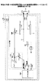
セレクタ130は、第1選択部の一例である。セレクタ130は、3つの入力端子と1つの出力端子とを有する。セレクタ130の3つの入力端子は、定電流源120の出力端子、電圧バッファ150の出力端子、及び電源VDDに接続されている。セレクタ130の出力端子は、端子102Aと、セレクタ180Aの2つの入力端子のうちの一方の入力端子とに接続されている。
The
セレクタ130の選択信号入力端子には、デジタル部100Dから端子101Eを介して、選択信号(Iref, Rx Term or Tx Term)が入力される。セレクタ130は、選択信号Irefが入力されると、定電流源120を選択する。
A selection signal (Iref, Rx Term or Tx Term) is input to the selection signal input terminal of the
また、セレクタ130は、選択信号Rx Termが入力されると、電圧バッファ150を選択する。また、セレクタ130は、選択信号Tx Termが入力されると、電源VDDを選択する。
The
セレクタ140は、第2選択部の一例である。セレクタ140は、3つの入力端子と、1つの出力端子とを有する。セレクタ140の出力端子は、端子102Bと、セレクタ180Aの2つの入力端子のうちの他方の入力端子とに接続される。
The
セレクタ140の3つの入力端子には、接地電位点、定電流源121、及び定電流源122が接続される。
A ground potential point, a constant
セレクタ140の選択信号入力端子には、デジタル部100Dから端子101Eを介して、選択信号(Iref, Rx Term or Tx Term)が入力される。セレクタ140は、選択信号Irefが入力されると、接地電位点を選択する。
A selection signal (Iref, Rx Term or Tx Term) is input to the selection signal input terminal of the
また、セレクタ140は、選択信号Rx Termが入力されると、定電流源121を選択する。また、セレクタ140は、選択信号Tx Termが入力されると、定電流源122を選択する。
In addition, the
電圧バッファ150は、第1電源の一例であり、オペアンプ151オペアンプ151を有する。オペアンプ151の非反転入力端子には終端電圧VDRが入力される。終端電圧VDRの電圧源は、例えば、電源VDDと電源VSSの間に接続した分圧回路であればよい。終端電圧VDRは、図2に示すレシーバ53A1、53A2、53B1、53B2が最適な動作点(電圧)でデータを受信できる任意の電圧に設定される。
The
オペアンプ151の反転入力端子は、自己の出力端子に接続されている。また、オペアンプ151の出力端子は、自己の非反転入力端子に接続されるとともに、セレクタ130の1つの入力端子と、終端抵抗部160の入力端子とに接続される。
The inverting input terminal of the
オペアンプ151は、終端電圧VDRをセレクタ130の1つの入力端子と、終端抵抗部160の入力端子とに出力する。なお、オペアンプ151の出力端子は、電圧バッファ150の出力端子である。電圧バッファ150が出力する終端電圧VDRは、第1電圧の一例である。
The
終端抵抗部160は、入力端子が電圧バッファ150に接続され、出力端子が定電流源123と、セレクタ180Bの3つの入力端子のうちの1つの入力端子とに接続される。終端抵抗部160は、第1可変抵抗部又は可変抵抗部の一例である。
終端抵抗部160は、図2に示すレシーバ53A1、53A2、53B1、53B2の終端抵抗部64A1、64A2、64B1、64B2に含まれる一対の可変抵抗器と同様の可変抵抗器である。より具体的には、終端抵抗部160は、図3(B)に示す終端抵抗部90Bと同様の回路構成を有する。
The
終端抵抗部160の終端抵抗値は、デジタル部100Dから端子101Bを介して入力される受信調整コードによって調整される。
The termination resistance value of the
終端抵抗部160の終端抵抗値の目標値は、50Ωである。終端抵抗部160の終端抵抗値は、受信側終端抵抗調整モードにおいて目標値に設定される。受信側終端抵抗調整モードでは、セレクタ130は、電圧バッファ150を選択し、セレクタ140は定電流源121を選択する。また、セレクタ180Aは端子102Bを選択し、セレクタ180Bは、終端抵抗部160と定電流源123との接続点を選択する。
The target value of the termination resistance value of the
このため、受信側終端抵抗調整モードでは、コンパレータ190は、基準抵抗器70での電圧降下と、終端抵抗部160での電圧降下とを比較することになり、デジタル部100Dは、基準抵抗器70での電圧降下と、終端抵抗部160での電圧降下とが等しくなるように、受信調整コードを調整する。
For this reason, in the reception-side termination resistance adjustment mode, the
従って、受信側終端抵抗調整モードにおいて終端抵抗部160に接続される定電流源123の電流値は、定電流源121の出力電流(Iref×1/2)に、基準抵抗器70の抵抗値(1kΩ)に対する終端抵抗部160の終端抵抗値の目標値(50Ω)の逆比倍(20倍)した電流値(Iref×10)に設定されている。
Therefore, the current value of the constant
終端抵抗部170は、電源VDDに接続され、出力端子が定電流源124と、セレクタ180Bの3つの入力端子のうちの1つの入力端子とに接続される。終端抵抗部170は、第2可変抵抗部の一例である。
終端抵抗部170は、図2に示すドライバ51A1、51A2、51B1、51B2の終端抵抗部62A1、62A2、62B1、62B2の一対の可変抵抗器と同様の可変抵抗器である。より具体的には、終端抵抗部170は、図3(A)に示す終端抵抗部90Aと同様の回路構成を有する。
The
終端抵抗部170の終端抵抗値は、デジタル部100Dから端子101Cを介して入力される送信調整コードによって調整される。
The termination resistance value of the
終端抵抗部170の終端抵抗値の目標値は、50Ωである。終端抵抗部170の終端抵抗値は、送信側終端抵抗調整モードにおいて目標値に設定される。送信側終端抵抗調整モードでは、セレクタ130は、電源VDDを選択し、セレクタ140は定電流源122を選択する。また、セレクタ180Aは端子102Bを選択し、セレクタ180Bは、終端抵抗部170と定電流源124との接続点を選択する。
The target value of the termination resistance value of the
このため、送信側終端抵抗調整モードでは、コンパレータ190は、基準抵抗器70での電圧降下と、終端抵抗部170での電圧降下とを比較することになり、デジタル部100Dは、基準抵抗器70での電圧降下と、終端抵抗部170での電圧降下とが等しくなるように、送信調整コードを調整する。
For this reason, in the transmission-side termination resistance adjustment mode, the
従って、送信側終端抵抗調整モードにおいて終端抵抗部170に接続される定電流源124の電流値は、定電流源122の出力電流(Iref×1)に、基準抵抗器70の抵抗値(1kΩ)に対する終端抵抗部170の終端抵抗値の目標値(50Ω)の逆比倍(20倍)した電流値(Iref×20)に設定されている。
Therefore, the current value of the constant
セレクタ180Aは、第3選択部の一例であり、2つの入力端子の一方がセレクタ130の出力端子と、端子102Aとに接続される。また、セレクタ180Aの他方の入力端子は、セレクタ140の出力端子と、端子102Bとに接続される。また、セレクタ180Aの出力端子は、コンパレータ190の非反転入力端子に接続される。
The
セレクタ180Aの選択信号入力端子には、デジタル部100Dから端子101Eを介して、選択信号(Iref, Rx Term or Tx Term)が入力される。セレクタ180Aは、選択信号Irefが入力されると、端子102Aを選択する。
A selection signal (Iref, Rx Term or Tx Term) is input to the selection signal input terminal of the
また、セレクタ180Aは、選択信号Rx Termが入力されると、端子102Bを選択する。また、セレクタ180Aは、選択信号Tx Termが入力されると、端子102Bを選択する。
The
セレクタ180Bは、第4選択部の一例であり、3つの入力端子の一つに基準電圧Vref2が入力される。基準電圧Vref2の電圧源181としては、例えば、バンドギャップリファレンス回路を用いればよい。基準電圧Vref2は、最終的な電流調整コードの値を決定する際に、コンパレータ190の反転入力端子に入力される基準電圧であり、基準電流生成回路110の基準電流を設定するために用いられる。電圧源181は第2電源の一例である。
The
また、セレクタ180Bのもう1つの入力端子は、終端抵抗部160と定電流源123との接続点に接続される。また、セレクタ180Bの残りの1つの入力端子は、終端抵抗部170と定電流源124との接続点に接続される。
The other input terminal of the
また、セレクタ180Bの出力端子は、コンパレータ190の反転入力端子に接続される。
The output terminal of the
セレクタ180Bの選択信号入力端子には、デジタル部100Dから端子101Eを介して、選択信号(Iref, Rx Term or Tx Term)が入力される。セレクタ180Bは、選択信号Irefが入力されると、基準電圧Vref2を選択する。
The selection signal (Iref, Rx Term or Tx Term) is input from the digital unit 100D to the selection signal input terminal of the
また、セレクタ180Bは、選択信号Rx Termが入力されると、終端抵抗部160と定電流源123との接続点を選択する。また、セレクタ180は、選択信号Tx Termが入力されると、終端抵抗部170と定電流源124との接続点を選択する。
In addition, when the selection signal Rx Term is input, the
コンパレータ190は、比較部の一例であり、非反転入力端子がセレクタ180Aの出力端子に接続され、反転入力端子がセレクタ180Bの出力端子に接続され、出力端子が端子101Dを介してデジタル部100Dに接続されている。
The
コンパレータ190は、非反転入力端子に入力されるセレクタ180Aの出力と、反転入力端子に入力されるセレクタ180Bの出力とを比較し、比較結果を表す信号をデジタル部100Dに出力する。
The
なお、以下では、一例として、基準電流生成回路110のオペアンプ113の反転入力端子に入力される基準電圧Vref1は800mV、セレクタ180Bに入力される基準電圧Vref2は400mV、電圧バッファ150の出力電圧VDRは600mV、電源VDDの電源電圧VDDは1Vとする。
In the following, as an example, the reference voltage Vref1 input to the inverting input terminal of the
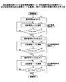
次に、上述のような構成の抵抗調整回路100の基準電流調整モード、受信側終端抵抗調整モード、及び送信側終端抵抗調整モードにおける動作を図6乃至9を用いて説明する。 Next, operations in the reference current adjustment mode, the reception-side termination resistance adjustment mode, and the transmission-side termination resistance adjustment mode of the resistance adjustment circuit 100 configured as described above will be described with reference to FIGS.
図6は、抵抗調整回路100の基準電流調整モード、受信側終端抵抗調整モード、及び送信側終端抵抗調整モードを選択し、実行する際の処理の流れを示す図である。図6に示す処理は、デジタル部100Dによって実行される。 FIG. 6 is a diagram illustrating a process flow when selecting and executing the reference current adjustment mode, the reception-side termination resistance adjustment mode, and the transmission-side termination resistance adjustment mode of the resistance adjustment circuit 100. The process shown in FIG. 6 is executed by the digital unit 100D.
図7は、実施の形態1の抵抗調整回路100の基準電流調整モードにおける接続関係を示す図である。図8は、実施の形態1の抵抗調整回路100の受信側終端抵抗調整モードにおける接続関係を示す図である。図9は、実施の形態1の抵抗調整回路100の送信側終端抵抗調整モードにおける接続関係を示す図である。 FIG. 7 is a diagram illustrating a connection relationship in the reference current adjustment mode of the resistance adjustment circuit 100 according to the first embodiment. FIG. 8 is a diagram illustrating a connection relationship in the reception-side termination resistance adjustment mode of the resistance adjustment circuit 100 according to the first embodiment. FIG. 9 is a diagram illustrating a connection relationship in the transmission-side termination resistance adjustment mode of the resistance adjustment circuit 100 according to the first embodiment.
図6に示すように、デジタル部100Dは、調整を開始すると、まず、選択信号Irefを出力する(ステップS1)。これにより、基準電流調整モードが実行される。 As shown in FIG. 6, when the adjustment starts, the digital unit 100D first outputs a selection signal Iref (step S1). Thereby, the reference current adjustment mode is executed.
基準電流調整モードにおいて、アナログ部100Aでは、図7に示すように、セレクタ130は定電流源120を選択し、セレクタ140は接地電位点を選択する。また、セレクタ180A及び180B(図5参照)は、それぞれ、端子102A及び基準電圧Vref2を選択する。
In the reference current adjustment mode, in the analog unit 100A, as shown in FIG. 7, the
このため、アナログ部100Aでは、図7に示すように、基準抵抗器70に定電流源120の電流(Iref×1)が流れる。この結果、基準抵抗器70の両端間には、電圧V1 = Iref × Rref = Iref × 1kΩが生じる。
Therefore, in the analog unit 100A, the current (Iref × 1) of the constant
このとき、コンパレータ190は、電圧V1と基準電圧Vref2との比較結果を表す信号を端子101Dを介してデジタル部100Dに出力する。
At this time, the
デジタル部100Dは、コンパレータ190から入力される比較結果を表す信号に基づき、基準電流生成回路110に入力する電流調整コードを調整する(ステップS2)。これにより、基準電流Irefの電流値が調整される。
The digital unit 100D adjusts the current adjustment code input to the reference
デジタル部100Dは、電圧V1と基準電圧Vref2が等しいかどうか比較する(ステップS3)。 The digital unit 100D compares whether the voltage V1 is equal to the reference voltage Vref2 (step S3).
デジタル部100Dは、電圧V1と基準電圧Vref2が等しくない(S3:NO)と判定すると、フローをステップS2にリターンし、電流調整コードを調整する。 If the digital unit 100D determines that the voltage V1 and the reference voltage Vref2 are not equal (S3: NO), the digital unit 100D returns the flow to step S2 and adjusts the current adjustment code.
この結果、ステップS2及びS3の処理は、電圧V1と基準電圧Vref2が等しくなるまで繰り返し実行される。これにより、最終的な電流調整コードの値が設定される。 As a result, the processes in steps S2 and S3 are repeatedly executed until the voltage V1 and the reference voltage Vref2 become equal. Thereby, the final value of the current adjustment code is set.
例えば、基準電流Irefの目標値を400uAとし、400uAの基準電流Irefを生成するためには、基準電圧Vref2は400mVに設定すればよい。 For example, in order to set the target value of the reference current Iref to 400 uA and generate the reference current Iref of 400 uA, the reference voltage Vref2 may be set to 400 mV.
デジタル部100Dは、電圧V1と基準電圧Vref2が等しい(S3:YES)と判定すると、基準電流調整モードを終了する。この結果、基準抵抗器70を用いて調整された基準電流Irefが基準電流生成回路110の可変抵抗器112に流れ、基準電流Irefをコピーした電流(Iref×1)が定電流源120から出力される。
If the digital unit 100D determines that the voltage V1 and the reference voltage Vref2 are equal (S3: YES), the digital unit 100D ends the reference current adjustment mode. As a result, the reference current Iref adjusted using the
なお、ステップS1からS3の処理により、定電流源121、122、123、124の電流も設定される。
Note that the currents of the constant
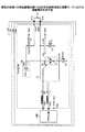
次に、デジタル部100Dは、受信側終端抵抗調整モードを実行するために、選択信号Rx Termを出力する(ステップS4)。 Next, the digital unit 100D outputs a selection signal Rx Term in order to execute the reception-side termination resistance adjustment mode (step S4).
受信側終端抵抗調整モードにおいて、アナログ部100Aでは、図8に示すように、セレクタ130は電圧バッファ150を選択し、セレクタ140は定電流源121を選択する。また、セレクタ180A及び180B(図5参照)は、それぞれ、端子102Bと、終端抵抗部160と定電流源123との接続点とを選択する。また、電圧バッファ150の出力電圧は、終端抵抗部160と基準抵抗器70とに印加される。
In the reception-side termination resistance adjustment mode, in the analog unit 100A, the
このため、図8に示すように、基準抵抗器70には定電流源121によって引き抜かれる電流(Iref×1/2)が流れる。また、終端抵抗部160には、定電流源123によって引き抜かれる電流(Iref×10)が流れる。
For this reason, as shown in FIG. 8, a current (Iref × 1/2) drawn by the constant
このとき、コンパレータ190は、端子102Bの電圧V2と、終端抵抗部160と定電流源123との接続点の電圧Vout_Rxとの比較結果を表す信号を端子101Dを介してデジタル部100Dに出力する。
At this time, the
デジタル部100Dは、コンパレータ190から入力される比較結果を表す信号に基づき、終端抵抗部160に入力する受信調整コードを調整する(ステップS5)。これにより、受信(Rx)側の終端抵抗部160の抵抗値が調整される。
The digital unit 100D adjusts the reception adjustment code input to the
デジタル部100Dは、端子102Bの電圧V2と、終端抵抗部160及び定電流源123の接続点の電圧Vout_Rxとが等しいかどうか比較する(ステップS6)。
The digital unit 100D compares whether or not the voltage V2 at the terminal 102B is equal to the voltage Vout_Rx at the connection point between the
デジタル部100Dは、電圧V2と電圧Vout_Rxとが等しくない(S6:NO)と判定すると、フローをステップS5にリターンし、受信調整コードを調整する。 If the digital unit 100D determines that the voltage V2 and the voltage Vout_Rx are not equal (S6: NO), the digital unit 100D returns the flow to step S5 and adjusts the reception adjustment code.
この結果、ステップS5及びS6の処理は、端子102Bの電圧V2と電圧Vout_Rxが等しくなるまで繰り返し実行される。これにより、最終的な受信調整コードが決定される。 As a result, the processes in steps S5 and S6 are repeatedly executed until the voltage V2 and the voltage Vout_Rx at the terminal 102B become equal. Thereby, a final reception adjustment code is determined.
デジタル部100Dは、電圧V2と電圧Vout_Rxが等しい(S6:YES)と判定すると、受信側終端抵抗調整モードを終了する。 If the digital unit 100D determines that the voltage V2 is equal to the voltage Vout_Rx (S6: YES), the digital unit 100D ends the reception-side termination resistance adjustment mode.
ここで、端子102Bの電圧V2と、終端抵抗部160及び定電流源123の接続点の電圧Vout_Rxとは、次のように求まる。なお、終端抵抗部160の終端抵抗値をRRxとする。
Here, the voltage V2 of the terminal 102B and the voltage Vout_Rx at the connection point of the
端子102Bの電圧V2は、V2 = VDR - Rref × (Iref×1/2)である。また、終端抵抗部160及び定電流源123の接続点の電圧Vout_Rxは、Vout_Rx = VDR - RRx × Iref × 10である。従って、ステップS6では、端子102Bの電圧V2と、終端抵抗部160及び定電流源123の接続点の電圧Vout_Rxとが等しくなるように、受信調整コードの値を調整して、終端抵抗部160の終端抵抗値をRRxを設定すればよい。
The voltage V2 at the terminal 102B is V2 = VDR−Rref × (Iref × 1/2). Further, the voltage Vout_Rx at the connection point between the
換言すれば、受信側終端抵抗調整モードでは、コンパレータ190は、基準抵抗器70での電圧降下と、終端抵抗部160での電圧降下とを比較することになり、デジタル部100Dは、基準抵抗器70での電圧降下と、終端抵抗部160での電圧降下とが等しくなるように、受信調整コードを調整する。
In other words, in the reception-side termination resistance adjustment mode, the
定電流源121の出力電流(Iref×1/2)と、定電流源123の出力電流(Iref×10)との比は、20倍であるため、終端抵抗部160の終端抵抗値をRRxは、基準抵抗器70の抵抗値Rref(1kΩ)に、逆比(1/20)を乗じた50Ωに設定される。これは、終端抵抗部160の終端抵抗値RRxの目標値である。
Since the ratio of the output current (Iref × 1/2) of the constant
例えば、V2 = VDR - Rref × (Iref×1/2) = 600mV-(1k×200uA)=400mVである。調整前の終端抵抗部160の終端抵抗値RRxは適当な値になっているため、終端抵抗部160及び定電流源123の接続点の電圧Vout_RxはV2とは異なり、電圧差が存在する。
For example, V2 = VDR−Rref × (Iref × 1/2) = 600 mV− (1 k × 200 uA) = 400 mV. Since the termination resistance value RRx of the
その電圧差をコンパレータ190で比較し、その結果を元に受信調整コードを調整することにより、終端抵抗部160の終端抵抗値RRxを増減させる。この結果、最終的にはVout_Rx = VDR - RRx × Iref × 10 = 600mV-50×10×400uA=400mVとなり、V2と一致する。この結果、終端抵抗部160の終端抵抗値RRxは、目標値の50Ωに設定される。
The voltage difference is compared by the
実施の形態1の抵抗調整回路100は、受信側終端抵抗調整モードを実行する前に、基準電流調整モードで基準抵抗器70を用いて基準電流(Iref)を生成する。そして、受信側終端抵抗調整モードでは、基準電流調整モードで設定した基準電流(Iref)に基づく定電流源121の出力電流(Iref×1/2)と、基準抵抗器70と、電圧バッファ150とを用いて、最終的な受信調整コードを決定する。これは、実際の受信動作における動作点で受信調整コードを決定していることを表している。
The resistance adjustment circuit 100 according to the first embodiment generates the reference current (Iref) using the
従って、受信調整コードを正確に決定することができる。受信調整コードは、デジタル部100D(図5参照)から、端子100T1を介して、レシーバ53A1、53A2、53B1、53B2の終端抵抗部64A1、64A2、64B1、64B2に入力される。 Therefore, the reception adjustment code can be accurately determined. The reception adjustment code is input from the digital unit 100D (see FIG. 5) to the terminal resistor units 64A1, 64A2, 64B1, and 64B2 of the receivers 53A1, 53A2, 53B1, and 53B2 via the terminal 100T1.
次に、デジタル部100Dは、送信側終端抵抗調整モードを実行するために、選択信号Tx Termを出力する(ステップS7)。 Next, the digital unit 100D outputs a selection signal Tx Term in order to execute the transmission-side termination resistance adjustment mode (step S7).
送信側終端抵抗調整モードにおいて、アナログ部100Aでは、図9に示すように、セレクタ130は電源VDDを選択し、セレクタ140は定電流源122を選択する。また、セレクタ180A及び180B(図5参照)は、それぞれ、端子102Bと、終端抵抗部170と定電流源124との接続点とを選択する。また、電源VDDの出力電圧は、終端抵抗部170と基準抵抗器70とに印加される。
In the transmission-side termination resistance adjustment mode, in the analog unit 100A, as shown in FIG. 9, the
このため、図9に示すように、基準抵抗器70には定電流源122によって引き抜かれる電流(Iref×1)が流れる。また、終端抵抗部170には、定電流源124によって引き抜かれる電流(Iref×20)が流れる。
For this reason, as shown in FIG. 9, a current (Iref × 1) drawn by the constant
このとき、コンパレータ190は、端子102Bの電圧V3と、終端抵抗部170と定電流源124との接続点の電圧Vout_Txとの比較結果を表す信号を端子101Dを介してデジタル部100Dに出力する。
At this time, the
デジタル部100Dは、コンパレータ190から入力される比較結果を表す信号に基づき、終端抵抗部170に入力する送信調整コードを調整する(ステップS8)。これにより、送信(Tx)側の終端抵抗部170の抵抗値が調整される。
The digital unit 100D adjusts the transmission adjustment code input to the
デジタル部100Dは、端子102Bの電圧V3と、終端抵抗部170及び定電流源124の接続点の電圧Vout_Txとが等しいかどうか比較する(ステップS9)。
The digital unit 100D compares whether the voltage V3 of the terminal 102B is equal to the voltage Vout_Tx at the connection point between the
デジタル部100Dは、電圧V3と電圧Vout_Txとが等しくない(S9:NO)と判定すると、フローをステップS8にリターンし、送信調整コードを調整する。 If the digital unit 100D determines that the voltage V3 and the voltage Vout_Tx are not equal (S9: NO), the digital unit 100D returns the flow to step S8 and adjusts the transmission adjustment code.
この結果、ステップS8及びS9の処理は、端子102Bの電圧V3と電圧Vout_Txが等しくなるまで繰り返し実行される。これにより、最終的な送信調整コードが決定される。 As a result, the processes in steps S8 and S9 are repeatedly executed until the voltage V3 and the voltage Vout_Tx at the terminal 102B become equal. Thereby, a final transmission adjustment code is determined.
デジタル部100Dは、電圧V3と電圧Vout_Txが等しい(S9:YES)と判定すると、送信側終端抵抗調整モードを終了する。 If the digital unit 100D determines that the voltage V3 and the voltage Vout_Tx are equal (S9: YES), the digital unit 100D ends the transmission-side termination resistance adjustment mode.
ここで、端子102Bの電圧V3と、終端抵抗部170及び定電流源124の接続点の電圧Vout_Txとは、次のように求まる。なお、終端抵抗部170の終端抵抗値をRTxとする。
Here, the voltage V3 of the terminal 102B and the voltage Vout_Tx at the connection point of the
端子102Bの電圧V3は、V3 = VDD - Rref × (Iref×1)である。また、終端抵抗部170及び定電流源124の接続点の電圧Vout_Txは、Vout_Tx = VDD - RTx × Iref × 20である。従って、ステップS9では、端子102Bの電圧V3と、終端抵抗部170及び定電流源124の接続点の電圧Vout_Txとが等しくなるように、送信調整コードの値を調整して、終端抵抗部170の終端抵抗値をRTxを設定すればよい。
The voltage V3 at the terminal 102B is V3 = VDD−Rref × (Iref × 1). The voltage Vout_Tx at the connection point between the
換言すれば、送信側終端抵抗調整モードでは、コンパレータ190は、基準抵抗器70での電圧降下と、終端抵抗部170での電圧降下とを比較することになり、デジタル部100Dは、基準抵抗器70での電圧降下と、終端抵抗部170での電圧降下とが等しくなるように、送信調整コードを調整する。
In other words, in the transmission-side termination resistance adjustment mode, the
定電流源122の出力電流(Iref×1)と、定電流源124の出力電流(Iref×20)との比は、20倍であるため、終端抵抗部170の終端抵抗値をRTxは、基準抵抗器70の抵抗値Rref(1kΩ)に、逆比(1/20)を乗じた50Ωに設定される。これは、終端抵抗部170の終端抵抗値RTxの目標値である。
Since the ratio of the output current (Iref × 1) of the constant
例えば、V3 = VDD - Rref × (Iref×1) = 1V-(1k×400uA)=600mVである。調整前の終端抵抗部170の終端抵抗値RTxは適当な値になっているため、終端抵抗部170及び定電流源124の接続点の電圧Vout_TxはV3とは異なり、電圧差が存在する。
For example, V3 = VDD−Rref × (Iref × 1) = 1V− (1k × 400uA) = 600 mV. Since the termination resistance value RTx of the
その電圧差をコンパレータ190で比較し、その結果を元に送信調整コードを調整することにより、終端抵抗部170の終端抵抗値RTxを増減させる。この結果、最終的にはVout_Tx = VDD - RTx × Iref × 20 = 1V-50×20×400uA=600mVとなり、V3と一致する。この結果、終端抵抗部170の終端抵抗値RTxは、目標値の50Ωに設定される。
The voltage difference is compared by the
このように、送信調整コードを正確に決定することができる。送信調整コードは、デジタル部100D(図5参照)から、端子100T2を介して、ドライバ51A1、51A2、51B1、51B2の終端抵抗部62A1、62A2、62B1、62B2に入力される。 In this way, the transmission adjustment code can be determined accurately. The transmission adjustment code is input from the digital unit 100D (see FIG. 5) to the terminal resistor units 62A1, 62A2, 62B1, and 62B2 of the drivers 51A1, 51A2, 51B1, and 51B2 via the terminal 100T2.
以上、実施の形態1の抵抗調整回路100は、受信側終端抵抗調整モードにおいて、基準電流生成回路110の基準電流に基づく電流を出力する定電流源121及び123と、基準抵抗器70と、電圧バッファ150とを用いる。これにより、電圧バッファ150の任意の受信側の終端電圧VDRに応じて、受信側の終端抵抗部160の終端抵抗値RRxを目標値の50Ωに設定することができる。
As described above, the resistance adjustment circuit 100 according to the first embodiment includes the constant
すなわち、レシーバ53A1、53A2、53B1、53B2の最適な動作電圧である任意の受信側の終端電圧VDRと、ドライバ53A1、53A2、53B1、53B2の電源電圧VDDとが異なる場合においても、終端電圧VDRに合わせて、終端抵抗部160の終端抵抗値RRxを目標値の50Ωに高精度に設定することができる。
That is, even when the termination voltage VDR on the receiving side, which is the optimum operating voltage of the receivers 53A1, 53A2, 53B1, and 53B2, and the power supply voltage VDD of the drivers 53A1, 53A2, 53B1, and 53B2 are different, the termination voltage VDR is In addition, the termination resistance value RRx of the
従って、実施の形態1によれば、任意の受信側の終端電圧VDRに応じて、受信(Rx)側の終端抵抗値を高精度に設定できる抵抗調整回路100を提供することができる。 Therefore, according to the first embodiment, it is possible to provide the resistance adjustment circuit 100 that can set the termination resistance value on the reception (Rx) side with high accuracy in accordance with the termination voltage VDR on the arbitrary reception side.
また、上述のステップS4〜S6の処理を行うことにより、終端抵抗値を高精度に設定できるので、実施の形態1によれば、受信(Rx)側の終端抵抗値を高精度に設定できる抵抗調整方法を提供することができる。 In addition, since the termination resistance value can be set with high accuracy by performing the processes of steps S4 to S6 described above, according to the first embodiment, the termination resistance value on the reception (Rx) side can be set with high accuracy. An adjustment method can be provided.
実施の形態1の抵抗調整回路100における受信側終端抵抗調整モードは、基準電流調整モード(ステップS1〜S3参照)を行った後に行われる。基準電流調整モードでは、基準抵抗器70を用いて、基準電流生成回路110が出力する基準電流(Iref)を設定する。
The reception-side termination resistance adjustment mode in the resistance adjustment circuit 100 of the first embodiment is performed after the reference current adjustment mode (see steps S1 to S3). In the reference current adjustment mode, the
そして、基準電流調整モードで基準電流(Iref)を設定した後に、基準電流(Iref)に基づく電流を出力する定電流源121及び123と、基準抵抗器70と、電圧バッファ150とを用いて終端抵抗部160の終端抵抗値RRxを調整するので、終端抵抗値RRxを目標値の50Ωに高精度に設定することができる。
Then, after setting the reference current (Iref) in the reference current adjustment mode, termination is performed using the constant
また、実施の形態1の抵抗調整回路100は、送信側終端抵抗調整モードでは、基準電流生成回路110の基準電流に基づく電流を出力する定電流源122及び124と、基準抵抗器70と、電源電圧VDDとを用いることにより、送信側の終端抵抗部170の終端抵抗値RTxを目標値の50Ωに設定することができる。
In addition, the resistance adjustment circuit 100 according to the first embodiment includes constant
従って、実施の形態1によれば、送信(Tx)側の終端抵抗値を高精度に設定できる抵抗調整回路100を提供することができる。 Therefore, according to the first embodiment, it is possible to provide the resistance adjustment circuit 100 that can set the terminating resistance value on the transmission (Tx) side with high accuracy.
なお、図6には、基準電流調整モード(S1〜S3)を行い、受信側終端抵抗調整モード(S4〜S6)を行った後に、送信側終端抵抗調整モード(S7〜S9)を行う形態について説明した。 FIG. 6 shows a mode in which the reference-current adjustment mode (S1 to S3) is performed, the transmission-side termination resistance adjustment mode (S7 to S9) is performed after the reception-side termination resistance adjustment mode (S4 to S6) is performed. explained.
しかしながら、受信側終端抵抗調整モード(S4〜S6)と、送信側終端抵抗調整モード(S7〜S9)との順番を入れ替えてもよい。 However, the order of the reception-side termination resistance adjustment mode (S4 to S6) and the transmission-side termination resistance adjustment mode (S7 to S9) may be switched.
また、以上では、受信側終端抵抗調整モードにおいて、基準電流生成回路110の基準電流に基づく電流を出力する定電流源121及び123を用いることにより、受信側の終端抵抗部160の終端抵抗値RRxを目標値の50Ωに設定する形態について説明した。
Further, in the above, by using the constant
しかしながら、基準電流を生成する回路は、基準電流生成回路110のような回路構成に限られない。定電流源121及び123が、基準抵抗器70を用いて設定した基準電流に基づく電流値の電流を出力できるのであれば、基準電流を生成する回路は、図5に示す基準電流生成回路110とは異なる回路であってもよい。
However, the circuit that generates the reference current is not limited to the circuit configuration like the reference
また、以上では、セレクタ180A、180Bで、コンパレータ190の入力信号を選択する形態について説明した。
In the above description, the
しかしながら、セレクタ180A、180Bを用いずに、3つのコンパレータ190を用いることにより、基準電流調整モード、受信側終端抵抗調整モード、送信側終端抵抗調整モードを行ってもよい。
However, the reference current adjustment mode, the reception-side termination resistance adjustment mode, and the transmission-side termination resistance adjustment mode may be performed by using the three
また、以上で説明した実施の形態1の抵抗調整回路100では、1つの基準抵抗器70を用いて、基準電流調整モードにおける基準電流の設定と、受信側終端抵抗調整モードにおける受信側の終端抵抗値の設定とを行うことができる。
In the resistance adjustment circuit 100 according to the first embodiment described above, the reference current is set in the reference current adjustment mode and the reception-side termination resistance in the reception-side termination resistance adjustment mode using one
また、以上で説明した実施の形態1の抵抗調整回路100では、1つの基準抵抗器70を用いて、基準電流調整モードにおける基準電流の設定と、送信側終端抵抗調整モードにおける送信側の終端抵抗値の設定とを行うことができる。
In the resistance adjustment circuit 100 of the first embodiment described above, the reference current is set in the reference current adjustment mode and the transmission-side termination resistance in the transmission-side termination resistance adjustment mode using one
このように、1つの基準抵抗器70を用いて基準電流の設定と終端抵抗値の設定とを行うことができるので、任意の受信側の終端電圧VDRでの終端抵抗値の調整のためにLSI20の外部に設ける素子を最小限度に抑えることができる。例えば、任意の受信側の終端電圧VDRでの終端抵抗値の調整のために電源等を追加する必要はない。
In this way, since the reference current and the termination resistance value can be set using one
従って、実施の形態1によれば、抵抗調整回路100の製造コストを抑えることができる。 Therefore, according to the first embodiment, the manufacturing cost of the resistance adjustment circuit 100 can be suppressed.
以上、実施の形態1の抵抗調整回路100によれば、基準電流生成回路110の基準電流に基づく電流を出力する定電流源121及び123と、基準抵抗器70と、電圧バッファ150とを用いることにより、任意の受信側の終端電圧VDRでの終端抵抗値を目標値の50Ωに設定することができるので、高品質なデータを受信することができる。
As described above, according to the resistance adjustment circuit 100 of the first embodiment, the constant
<実施の形態2>
図10は、実施の形態2の抵抗調整回路200を示す図である。
<
FIG. 10 is a diagram illustrating a
抵抗調整回路200は、アナログ部200A、デジタル部100D、及び端子200T1、200T2を含む。アナログ部200Aは、高速/高精度なCMO回路によって構築される。デジタル部100Dは、高速動作が可能なデジタル回路によって構築される。抵抗調整回路200は、図2に示す調整回路52A及び52Bに1つずつ含まれる。
The
実施の形態2の抵抗調整回路200は、実施の形態1の抵抗調整回路100の終端抵抗部160及び170を終端抵抗部260及び270に置き換えたものである。終端抵抗部260及び270は、電流源及び電位点との接続が実施の形態1の終端抵抗部160及び170と異なる。
The
また、終端抵抗部270は、PMOSトランジスタを含む終端抵抗部170とは異なり、NMOS(N channel Metal Oxide Semiconductor)トランジスタを含む。
The
また、実施の形態2の抵抗調整回路200には、上述の違いにより、その他の回路構成についても、実施の形態1の抵抗調整回路100の回路構成とは異なる部分がある。
In addition, the
以下、実施の形態1の抵抗調整回路100の構成要素と同様の構成要素には同一符号を付し、その説明を省略する。 Hereinafter, the same components as those of the resistance adjustment circuit 100 according to the first embodiment are denoted by the same reference numerals, and the description thereof is omitted.
図10では、抵抗調整回路200がLSI20の高速シリアルインターフェース50に含まれるものとして説明する。LSI20は、図2に示すLSI20A又は20Bに相当する。高速シリアルインターフェース50は、図2に示す高速シリアルインターフェース50A又は50Bに相当する。
In FIG. 10, the
また、抵抗調整回路200には、基準抵抗器70が接続されている。基準抵抗器70は、図2に示す基準抵抗器70A又は70Bに相当する。ここでは、基準抵抗器70の抵抗値Rrefが1kΩである場合について説明する。
A
なお、ここでは、基準抵抗器70は、LSI20の外部に設けられていて、抵抗調整回路200に接続されているものとして説明するが、基準抵抗器70は、抵抗調整回路200の構成要素として含まれていてもよい。
Here, the
抵抗調整回路200のアナログ部200Aは、端子201A、201B、201C、201D、201E、202A、202B、基準電流生成回路110、定電流源120、221、222、223、224、及びセレクタ230、240を含む。
The
抵抗調整回路200のアナログ部200Aは、さらに、電圧バッファ150、終端抵抗部260、270、セレクタ180A、180B、及びコンパレータ190を含む。
The
デジタル部100Dは、実施の形態1のデジタル部100Dと同様であり、デジタル部100Dの端子100D1、100D2、100D3、100D4、100D5は、それぞれ、アナログ部200Aの端子201A、201B、201C、201D、201Eに接続されている。端子100D4には、アナログ部200Aから比較結果が入力される。
The digital unit 100D is the same as the digital unit 100D of the first embodiment, and the terminals 100D1, 100D2, 100D3, 100D4, and 100D5 of the digital unit 100D are the
デジタル部100Dの端子100D6、100D7は、それぞれ、受信調整コード、送信調整コードを抵抗調整回路200の外部に出力するための端子である。端子100D6、100D7は、それぞれ、抵抗調整回路200の端子200T1、200T2に接続されている。
Terminals 100D6 and 100D7 of the digital unit 100D are terminals for outputting the reception adjustment code and the transmission adjustment code to the outside of the
端子200T1、200T2は、図2に示す調整回路52A及び52Bから受信調整コード及び送信調整コードが出力される端子に相当する。
Terminals 200T1 and 200T2 correspond to terminals from which reception adjustment codes and transmission adjustment codes are output from
端子201A、201B、201C、201D、201Eは、デジタル部100Dに接続される端子である。
端子201Aは、デジタル部100Dから電流調整コードが入力される端子である。端子201Aは、基準電流生成回路110の可変抵抗器112のコード入力端子に接続されている。デジタル部100Dは、端子201Aを介して、可変抵抗器112に電流調整コードを入力する。電流調整コードは、基準電流生成回路110の出力電流値を調整するコードである。
The terminal 201A is a terminal to which a current adjustment code is input from the digital unit 100D. The terminal 201A is connected to the code input terminal of the
端子201Bは、デジタル部100Dから受信調整コードが入力される端子である。端子201Bは、終端抵抗部260のコード入力端子に接続されている。デジタル部100Dは、端子201Bを介して、終端抵抗部260に受信調整コードを入力する。受信調整コードは、終端抵抗部260の終端抵抗値を調整するコードである。
The terminal 201B is a terminal to which a reception adjustment code is input from the digital unit 100D. The terminal 201B is connected to the code input terminal of the
端子201Cは、デジタル部100Dから送信調整コードが入力される端子である。端子201Cは、終端抵抗部270のコード入力端子に接続されている。デジタル部100Dは、端子201Cを介して、終端抵抗部270に送信調整コードを入力する。送信調整コードは、終端抵抗部270の終端抵抗値を調整するコードである。
The terminal 201C is a terminal to which a transmission adjustment code is input from the digital unit 100D. The terminal 201C is connected to the cord input terminal of the
端子201Dは、デジタル部100Dにコンパレータ190の比較結果を表す信号を出力する端子である。端子201Dは、コンパレータ190の出力端子に接続されている。コンパレータ190の比較結果を表す信号は、端子201Dを介して、デジタル部100Dに出力される。
The terminal 201D is a terminal that outputs a signal representing the comparison result of the
端子201Eは、デジタル部100Dから選択信号(Iref, Rx Term or Tx Term)が入力される端子である。端子201Eは、セレクタ230、240、180A、180Bの選択信号入力端子に接続されている。デジタル部100Dは、端子201Eを介して、選択信号(Iref, Rx Term or Tx Term)をセレクタ230、240、180A、180Bの選択信号入力端子に入力する。
The terminal 201E is a terminal to which a selection signal (Iref, Rx Term or Tx Term) is input from the digital unit 100D. The
端子202Aは、アナログ部200Aの内部では、セレクタ230の出力端子と、セレクタ180Aの一方の入力端子とに接続される。また、端子202Aは、アナログ部200Aの外部では、LSI20の端子21Aを介して、基準抵抗器70の一方の端子に接続される。
The terminal 202A is connected to the output terminal of the
端子202Bは、アナログ部200Aの内部では、セレクタ240の出力端子と、セレクタ180Aの他方の入力端子とに接続される。また、端子202Bは、アナログ部200Aの外部では、LSI20の端子21Bを介して、基準抵抗器70の他方の端子に接続される。
The terminal 202B is connected to the output terminal of the
なお、端子202A、202Bは、アナログ部200Aの端子であるとともに、抵抗調整回路200の端子でもある。
The
また、端子21A、21Bは、LSI20に基準抵抗器70を接続するための端子であり、図10において、端子21A、21Bよりも左側は、LSI20の内部であり、端子21A、21Bよりも右側は、LSI20の外部である。図10では、LSI20の外部に存在するのは、基準抵抗器70のみである。
基準電流生成回路110は、抵抗調整回路200が終端抵抗部260及び270における受信側の終端抵抗値、及び、送信側の終端抵抗値をそれぞれ設定する際に用いる基準電流を生成する回路である。
The reference
定電流源120は、電源VDDとセレクタ230の3つの入力端子のうちの1つとの間に接続されている。定電流源120は、基準電流生成回路110とカレントミラー回路を構築する。
The constant
定電流源221、222、223、224は、定電流源120と同様に、基準電流生成回路110とカレントミラー回路を構築する。
The constant
定電流源221は、電源VDDと、セレクタ230の3つの入力端子のうちの1つとの間に接続されている。定電流源221は、基準電流生成回路110の基準電流Irefの半分の電流(Iref×1/2)を出力する。
The constant
定電流源222は、電源VDDと、セレクタ230の3つの入力端子のうちの1つとの間に接続されている。定電流源222は、基準電流生成回路110の基準電流Irefと等しい電流(Iref×1)を出力する。
The constant
定電流源223は、電源VDDと、終端抵抗部260との間に接続されている。定電流源223は、基準電流生成回路110の基準電流Irefの10倍の電流(Iref×10)を終端抵抗部260に出力する。
The constant
定電流源224は、電源VDDと、終端抵抗部270との間に接続されている。定電流源224は、基準電流生成回路110の基準電流Irefの20倍の電流(Iref×20)を終端抵抗部270に出力する。
The constant
セレクタ230は、3つの入力端子と1つの出力端子とを有する。セレクタ230の3つの入力端子は、定電流源120の出力端子、定電流源221の出力端子、及び定電流源222の出力端子に接続されている。セレクタ230の出力端子は、端子202Aと、セレクタ180Aの2つの入力端子のうちの一方の入力端子とに接続されている。
The
セレクタ230の選択信号入力端子には、デジタル部100Dから端子201Eを介して、選択信号(Iref, Rx Term or Tx Term)が入力される。セレクタ230は、選択信号Irefが入力されると、定電流源120を選択する。
A selection signal (Iref, Rx Term or Tx Term) is input to the selection signal input terminal of the
また、セレクタ230は、選択信号Rx Termが入力されると、定電流源221を選択する。また、セレクタ230は、選択信号Tx Termが入力されると、定電流源222を選択する。
The
セレクタ240は、1つの出力端子と、3つの入力端子とを有する。セレクタ240の出力端子は、端子202Bと、セレクタ180Aの2つの入力端子のうちの他方の入力端子とに接続される。
The
セレクタ240の3つの入力端子のうちの1つには、電圧バッファ150の出力端子が接続され、残りの2つの入力端子には、接地電位点が接続される。
The output terminal of the
セレクタ240の選択信号入力端子には、デジタル部100Dから端子201Eを介して、選択信号(Iref, Rx Term or Tx Term)が入力される。セレクタ240は、選択信号Irefが入力されると、接地電位点を選択する。
A selection signal (Iref, Rx Term or Tx Term) is input to the selection signal input terminal of the
また、セレクタ240は、選択信号Rx Termが入力されると、電圧バッファ150を選択する。また、セレクタ240は、選択信号Tx Termが入力されると、接地電位点を選択する。
Further, the
電圧バッファ150は、実施の形態1の電圧バッファ150と同様であるが、自己の出力端子が終端抵抗部260とセレクタ240の入力端子とに接続されている点が、実施の形態1の電圧バッファ150と異なる。
The
終端抵抗部260は、一端が電圧バッファ150に接続され、他端が定電流源223と、セレクタ180Bの3つの入力端子のうちの1つの入力端子とに接続される。
終端抵抗部260は、図2に示すレシーバ53A1、53A2、53B1、53B2の終端抵抗部64A1、64A2、64B1、64B2に含まれる一対の可変抵抗器と同様の可変抵抗器である。より具体的には、終端抵抗部260は、図3(B)に示す終端抵抗部90Bと同様の回路構成を有する。
The
終端抵抗部260の終端抵抗値は、デジタル部100Dから端子201Bを介して入力される受信調整コードによって調整される。
The termination resistance value of the
終端抵抗部260の終端抵抗値の目標値は、50Ωである。終端抵抗部260の終端抵抗値は、受信側終端抵抗調整モードにおいて目標値に設定される。受信側終端抵抗調整モードでは、セレクタ230は、定電流源221を選択し、セレクタ240は電圧バッファ150を選択する。また、セレクタ180Aは端子202Aを選択し、セレクタ180Bは、終端抵抗部260と定電流源223との接続点を選択する。
The target value of the termination resistance value of the
このため、受信側終端抵抗調整モードでは、コンパレータ190は、基準抵抗器70での電圧降下と、終端抵抗部260での電圧降下とを比較することになり、デジタル部100Dは、基準抵抗器70での電圧降下と、終端抵抗部260での電圧降下とが等しくなるように、受信調整コードを調整する。
For this reason, in the reception-side termination resistance adjustment mode, the
従って、受信側終端抵抗調整モードにおいて終端抵抗部260に接続される定電流源223の電流値は、定電流源221の出力電流(Iref×1/2)に、基準抵抗器70の抵抗値(1kΩ)に対する終端抵抗部260の終端抵抗値の目標値(50Ω)の逆比倍(20倍)した電流値(Iref×10)に設定されている。
Therefore, the current value of the constant
終端抵抗部270は、一端が接地電位点に接続され、他端が定電流源224と、セレクタ180Bの3つの入力端子のうちの1つの入力端子とに接続される。なお、終端抵抗部270の詳細な回路構成については、図11を用いて後述する。
終端抵抗部270の終端抵抗値は、デジタル部100Dから端子201Cを介して入力される送信調整コードによって調整される。
The termination resistance value of the
終端抵抗部270の終端抵抗値の目標値は、50Ωである。終端抵抗部270の終端抵抗値は、送信側終端抵抗調整モードにおいて目標値に設定される。送信側終端抵抗調整モードでは、セレクタ230は、定電流源222を選択し、セレクタ240は接地電位点を選択する。また、セレクタ180Aは端子202Aを選択し、セレクタ180Bは、終端抵抗部270と定電流源224との接続点を選択する。
The target value of the termination resistance value of the
このため、送信側終端抵抗調整モードでは、コンパレータ190は、基準抵抗器70での電圧降下と、終端抵抗部270での電圧降下とを比較することになり、デジタル部100Dは、基準抵抗器70での電圧降下と、終端抵抗部270での電圧降下とが等しくなるように、送信調整コードを調整する。
Therefore, in the transmission-side termination resistance adjustment mode, the
従って、送信側終端抵抗調整モードにおいて終端抵抗部270に接続される定電流源224の電流値は、定電流源222の出力電流(Iref×1)に、基準抵抗器70の抵抗値(1kΩ)に対する終端抵抗部270の終端抵抗値の目標値(50Ω)の逆比倍(20倍)した電流値(Iref×20)に設定されている。
Therefore, the current value of the constant
セレクタ180Aは、2つの入力端子の一方がセレクタ230の出力端子と、端子202Aとに接続される。また、セレクタ180Aの他方の入力端子は、セレクタ240の出力端子と、端子202Bとに接続される。また、セレクタ180Aの出力端子は、コンパレータ190の非反転入力端子に接続される。
In the
セレクタ180Aの選択信号入力端子には、デジタル部100Dから端子201Eを介して、選択信号(Iref, Rx Term or Tx Term)が入力される。セレクタ180Aは、選択信号Irefが入力されると、端子202Aを選択する。
The selection signal (Iref, Rx Term or Tx Term) is input from the digital unit 100D to the selection signal input terminal of the
また、セレクタ180Aは、選択信号Rx Termが入力されると、端子202Aを選択する。また、セレクタ180Aは、選択信号Tx Termが入力されると、端子202Aを選択する。
Further, the
セレクタ180Bは、3つの入力端子の一つに基準電圧Vref2が入力される。セレクタ180Bのもう1つの入力端子は、終端抵抗部260と定電流源223との接続点に接続される。また、セレクタ180Bの残りの1つの入力端子は、終端抵抗部270と定電流源224との接続点に接続される。また、セレクタ180Bの出力端子は、コンパレータ190の反転入力端子に接続される。
In the
セレクタ180Bの選択信号入力端子には、デジタル部100Dから端子201Eを介して、選択信号(Iref, Rx Term or Tx Term)が入力される。セレクタ180Bは、選択信号Irefが入力されると、基準電圧Vref2を選択する。
The selection signal (Iref, Rx Term or Tx Term) is input from the digital unit 100D to the selection signal input terminal of the
また、セレクタ180Bは、選択信号Rx Termが入力されると、終端抵抗部260と定電流源223との接続点を選択する。また、セレクタ180は、選択信号Tx Termが入力されると、終端抵抗部270と定電流源224との接続点を選択する。
Further, when the selection signal Rx Term is input, the
コンパレータ190は、非反転入力端子がセレクタ180Aの出力端子に接続され、反転入力端子がセレクタ180Bの出力端子に接続され、出力端子が端子201Dを介してデジタル部100Dに接続されている。
The
次に、図11を用いて、実施の形態2の終端抵抗部270について説明する。終端抵抗部270としては、例えば、図11に示す終端抵抗部90Cを用いればよい。
Next, the
図11は、実施の形態2の終端抵抗部90Cの回路構成を示す図である。
FIG. 11 is a diagram illustrating a circuit configuration of the
図11に示す終端抵抗部90Cは、端子90C1、90C2、及び、調整部91C1、91C2、91C3、91C4を含む。なお、端子90C2は、4つの調整部91C1、91C2、91C3、91C4に対応して4つ設けられている。
The
端子90C1は、接地電圧VSSと、調整部91C1、91C2、91C3、91C4の合成抵抗値とを反映した信号を出力する端子である。端子90C1は、図10に示す終端抵抗部270の可変抵抗器の上側の端子に相当する。
The terminal 90C1 is a terminal that outputs a signal reflecting the ground voltage VSS and the combined resistance value of the adjusting units 91C1, 91C2, 91C3, and 91C4. The terminal 90C1 corresponds to a terminal on the upper side of the variable resistor of the
端子90C2は、送信調整コードが入力される端子であり、図10に示す終端抵抗部270の終端抵抗部に送信調整コードが入力される端子に相当する。
The terminal 90C2 is a terminal to which a transmission adjustment code is input, and corresponds to a terminal to which the transmission adjustment code is input to the termination resistor unit of the
調整部91C1、91C2、91C3、91C4は、同様の構成を有する。 The adjustment units 91C1, 91C2, 91C3, and 91C4 have the same configuration.
調整部91C1は、抵抗器92C1、及びNMOSトランジスタ92C2を含む。 The adjustment unit 91C1 includes a resistor 92C1 and an NMOS transistor 92C2.
抵抗器92C1は、端子90C1と、NMOSトランジスタ92C2のドレインとの間に接続される。 The resistor 92C1 is connected between the terminal 90C1 and the drain of the NMOS transistor 92C2.
NMOSトランジスタ92C2は、ドレインが抵抗器92C1に接続され、ゲートが端子90C2に接続され、ソースがグランドVSSに接続される。 The NMOS transistor 92C2 has a drain connected to the resistor 92C1, a gate connected to the terminal 90C2, and a source connected to the ground VSS.
調整部91C2、91C3、91C4は、調整部91C1と同様の構成を有する。調整部91C1、91C2、91C3、91C4の抵抗器92C1は、端子90C1に対して並列に接続され、調整部91C1、91C2、91C3、91C4のNMOSトランジスタ92C2のゲートは、それぞれ、4つの端子90C2に接続される。 The adjustment units 91C2, 91C3, 91C4 have the same configuration as the adjustment unit 91C1. The resistors 92C1 of the adjustment units 91C1, 91C2, 91C3, and 91C4 are connected in parallel to the terminal 90C1, and the gates of the NMOS transistors 92C2 of the adjustment units 91C1, 91C2, 91C3, and 91C4 are connected to the four terminals 90C2, respectively. Is done.
終端抵抗部90Cは、4つの端子90C2に入力される送信調整コードによって、調整部91C1、91C2、91C3、91C4のNMOSトランジスタ92C2のオン/オフが調整される。
In the terminating
NMOSトランジスタ92C2がオンにされる調整部(91C1、91C2、91C3、91C4)の数が増えると、並列に接続される抵抗器92C1の数が増えるため、終端抵抗部90Cの合成抵抗値は低下する。
As the number of adjustment units (91C1, 91C2, 91C3, 91C4) in which the NMOS transistor 92C2 is turned on increases, the number of resistors 92C1 connected in parallel increases, so the combined resistance value of the
NMOSトランジスタ92C2がオンにされる調整部(91C1、91C2、91C3、91C4)の数が少なくなると、並列に接続される抵抗器92C1の数が減るため、終端抵抗部90Cの合成抵抗値は増大する。
When the number of adjustment units (91C1, 91C2, 91C3, 91C4) in which the NMOS transistor 92C2 is turned on decreases, the number of resistors 92C1 connected in parallel decreases, so that the combined resistance value of the
調整部91C1、91C2、91C3、91C4の各抵抗値と各トランジスタのサイズは、合成抵抗値が短調増減するように設計されていればよい。また、調整部の数はプロセスばらつきの調整範囲を確保するために調整部の数を増減してもよい。 The resistance values of the adjusting units 91C1, 91C2, 91C3, and 91C4 and the sizes of the transistors only have to be designed so that the combined resistance value is increased or decreased in minor. Further, the number of adjustment units may be increased or decreased in order to secure an adjustment range of process variation.
次に、上述のような構成の抵抗調整回路200の基準電流調整モード、受信側終端抵抗調整モード、及び送信側終端抵抗調整モードにおける回路の動作を図12乃至14を用いて説明する。
Next, the operation of the circuit in the reference current adjustment mode, the reception-side termination resistance adjustment mode, and the transmission-side termination resistance adjustment mode of the
図12は、実施の形態2の抵抗調整回路200の基準電流調整モードにおける接続関係を示す図である。図13は、実施の形態2の抵抗調整回路200の受信側終端抵抗調整モードにおける接続関係を示す図である。図14は、実施の形態2の抵抗調整回路200の送信側終端抵抗調整モードにおける接続関係を示す図である。
FIG. 12 is a diagram illustrating a connection relationship in the reference current adjustment mode of the
基準電流調整モードにおいて、アナログ部200Aでは、図12に示すように、セレクタ230は定電流源120を選択し、セレクタ240は接地電位点を選択する。また、セレクタ180A及び180B(図10参照)は、それぞれ、端子202A及び基準電圧Vref2を選択する。
In the reference current adjustment mode, in the
このため、アナログ部200Aでは、図12に示すように、基準抵抗器70に定電流源120の電流(Iref×1)が流れる。この結果、基準抵抗器70の両端間には、電圧V21 = Iref × Rref = Iref × 1kΩが生じる。
Therefore, in the
このとき、コンパレータ190は、電圧V21と基準電圧Vref2との比較結果を表す信号を端子201Dを介してデジタル部100Dに出力する。
At this time, the
デジタル部100Dは、コンパレータ190から入力される比較結果を表す信号に基づき、基準電流生成回路110に入力する電流調整コードを調整する。これにより、基準電流Irefの電流値が調整される。
The digital unit 100D adjusts the current adjustment code input to the reference
デジタル部100Dは、電圧V21と基準電圧Vref2が等しいかどうか比較し、電圧V21と基準電圧Vref2が等しくなるまで電流調整コードを調整する。これにより、最終的な電流調整コードの値が設定される。 The digital unit 100D compares the voltage V21 with the reference voltage Vref2 and adjusts the current adjustment code until the voltage V21 and the reference voltage Vref2 are equal. Thereby, the final value of the current adjustment code is set.
この結果、基準抵抗器70を用いて調整された基準電流Irefが基準電流生成回路110の可変抵抗器112に流れ、基準電流Irefをコピーした電流(Iref×1)が定電流源120から出力される。また、定電流源221、222、223、224の電流も設定される。
As a result, the reference current Iref adjusted using the
受信側終端抵抗調整モードでは、アナログ部200Aにおいては、図13に示すように、セレクタ230は定電流源221を選択し、セレクタ240は電圧バッファ150を選択する。また、セレクタ180A及び180B(図10参照)は、それぞれ、端子202Aと、終端抵抗部260と定電流源223との接続点とを選択する。また、電圧バッファ150の出力電圧は、終端抵抗部260と基準抵抗器70とに印加される。
In the reception-side termination resistance adjustment mode, in the
このため、図13に示すように、基準抵抗器70には定電流源221から出力される電流(Iref×1/2)が流れる。また、終端抵抗部260には、定電流源223から出力される電流(Iref×10)が流れる。
For this reason, as shown in FIG. 13, the current (Iref × 1/2) output from the constant
このとき、コンパレータ190は、端子202Aの電圧V22と、終端抵抗部260と定電流源223との接続点の電圧Vout_Rxとの比較結果を表す信号を端子201Dを介してデジタル部100Dに出力する。
At this time, the
デジタル部100Dは、コンパレータ190から入力される比較結果を表す信号に基づき、終端抵抗部260に入力する受信調整コードを調整する。これにより、受信(Rx)側の終端抵抗部260の抵抗値が調整される。
The digital unit 100 </ b> D adjusts the reception adjustment code input to the
デジタル部100Dは、端子202Aの電圧V22と、終端抵抗部260及び定電流源223の接続点の電圧Vout_Rxとが等しいかどうか比較し、端子202Aの電圧V22と電圧Vout_Rxが等しくなるまで受信調整コードを調整する。これにより、最終的な受信調整コードが決定される。
The digital unit 100D compares the voltage V22 of the terminal 202A with the voltage Vout_Rx at the connection point between the
デジタル部100Dは、電圧V22と電圧Vout_Rxが等しくなると、受信側終端抵抗調整モードを終了する。 When the voltage V22 and the voltage Vout_Rx become equal, the digital unit 100D ends the reception-side termination resistance adjustment mode.
ここで、端子202Aの電圧V22と、終端抵抗部260及び定電流源223の接続点の電圧Vout_Rxとは、次のように求まる。なお、終端抵抗部260の終端抵抗値をRRxとする。
Here, the voltage V22 of the terminal 202A and the voltage Vout_Rx at the connection point of the
端子202Aの電圧V22は、V22 = VDR + Rref × (Iref×1/2)である。また、終端抵抗部260及び定電流源223の接続点の電圧Vout_Rxは、Vout_Rx = VDR + RRx × Iref × 10である。従って、端子202Aの電圧V22と、終端抵抗部260及び定電流源223の接続点の電圧Vout_Rxとが等しくなるように、受信調整コードの値を調整して、終端抵抗部260の終端抵抗値をRRxを設定すればよい。
The voltage V22 at the terminal 202A is V22 = VDR + Rref × (Iref × 1/2). The voltage Vout_Rx at the connection point between the
換言すれば、受信側終端抵抗調整モードでは、コンパレータ190は、基準抵抗器70での電圧降下と、終端抵抗部260での電圧降下とを比較することになり、デジタル部100Dは、基準抵抗器70での電圧降下と、終端抵抗部260での電圧降下とが等しくなるように、受信調整コードを調整する。
In other words, in the reception-side termination resistance adjustment mode, the
定電流源221の出力電流(Iref×1/2)と、定電流源223の出力電流(Iref×10)との比は、20倍であるため、終端抵抗部260の終端抵抗値をRRxは、基準抵抗器70の抵抗値Rref(1kΩ)に、逆比(1/20)を乗じた50Ωに設定される。これは、終端抵抗部260の終端抵抗値RRxの目標値である。
Since the ratio of the output current (Iref × 1/2) of the constant
受信側終端抵抗調整モードでの処理の結果、終端抵抗部260の終端抵抗値RRxは、目標値の50Ωに設定される。
As a result of the processing in the reception-side termination resistance adjustment mode, the termination resistance value RRx of the
送信側終端抵抗調整モードでは、アナログ部200Aにおいて、図14に示すように、セレクタ230は定電流源222を選択し、セレクタ240は接地電位点を選択する。また、セレクタ180A及び180B(図10参照)は、それぞれ、端子202Aと、終端抵抗部270と定電流源224との接続点とを選択する。
In the transmission-side termination resistance adjustment mode, in the
このため、図14に示すように、基準抵抗器70には定電流源222から出力される電流(Iref×1)が流れる。また、終端抵抗部270には、定電流源224から出力される電流(Iref×20)が流れる。
Therefore, as shown in FIG. 14, the current (Iref × 1) output from the constant
このとき、コンパレータ190は、端子202Aの電圧V23と、終端抵抗部270と定電流源224との接続点の電圧Vout_Txとの比較結果を表す信号を端子201Dを介してデジタル部100Dに出力する。
At this time, the
デジタル部100Dは、コンパレータ190から入力される比較結果を表す信号に基づき、終端抵抗部270に入力する送信調整コードを調整する。これにより、送信(Tx)側の終端抵抗部270の抵抗値が調整される。
The digital unit 100 </ b> D adjusts the transmission adjustment code input to the
デジタル部100Dは、端子202Aの電圧V23と、終端抵抗部270及び定電流源224の接続点の電圧Vout_Txとが等しいかどうか比較し、端子202Aの電圧V23と電圧Vout_Txが等しくなるまで送信調整コードを調整する。これにより、最終的な送信調整コードが決定される。
The digital unit 100D compares the voltage V23 of the terminal 202A with the voltage Vout_Tx at the connection point between the
デジタル部100Dは、電圧V23と電圧Vout_Txが等しくなると、送信側終端抵抗調整モードを終了する。 When the voltage V23 and the voltage Vout_Tx become equal, the digital unit 100D ends the transmission-side termination resistance adjustment mode.
ここで、端子202Aの電圧V23と、終端抵抗部270及び定電流源224の接続点の電圧Vout_Txとは、次のように求まる。なお、終端抵抗部270の終端抵抗値をRTxとする。
Here, the voltage V23 of the terminal 202A and the voltage Vout_Tx at the connection point of the
端子202Aの電圧V23は、V23 = Rref × (Iref×1)である。また、終端抵抗部270及び定電流源224の接続点の電圧Vout_Txは、Vout_Tx = RTx × Iref × 20である。従って、端子202Aの電圧V23と、終端抵抗部270及び定電流源224の接続点の電圧Vout_Txとが等しくなるように、送信調整コードの値を調整して、終端抵抗部270の終端抵抗値をRTxを設定すればよい。
The voltage V23 at the terminal 202A is V23 = Rref × (Iref × 1). Further, the voltage Vout_Tx at the connection point between the
換言すれば、送信側終端抵抗調整モードでは、コンパレータ190は、基準抵抗器70での電圧降下と、終端抵抗部270での電圧降下とを比較することになり、デジタル部100Dは、基準抵抗器70での電圧降下と、終端抵抗部270での電圧降下とが等しくなるように、送信調整コードを調整する。
In other words, in the transmission-side termination resistance adjustment mode, the
定電流源222の出力電流(Iref×1)と、定電流源224の出力電流(Iref×20)との比は、20倍であるため、終端抵抗部270の終端抵抗値をRTxは、基準抵抗器70の抵抗値Rref(1kΩ)に、逆比(1/20)を乗じた50Ωに設定される。これは、終端抵抗部270の終端抵抗値RTxの目標値である。
Since the ratio of the output current (Iref × 1) of the constant
送信側終端抵抗調整モードの結果、終端抵抗部270の終端抵抗値RTxは、目標値の50Ωに設定される。
As a result of the transmission-side termination resistance adjustment mode, the termination resistance value RTx of the
以上、実施の形態2の抵抗調整回路200によれば、受信側終端抵抗調整モードにおいて、基準電流生成回路110の基準電流に基づく電流を出力する定電流源221及び223と、基準抵抗器70と、電圧バッファ150とを用いることにより、受信側の終端抵抗部260の終端抵抗値RRxを目標値の50Ωに高精度に設定することができる。
As described above, according to the
従って、実施の形態2によれば、実施の形態1と同様に、受信(Rx)側の終端抵抗値を高精度に設定できる抵抗調整回路200及び抵抗調整方法を提供することができる。
Therefore, according to the second embodiment, similar to the first embodiment, it is possible to provide the
また、実施の形態2によれば、実施の形態1と同様に、送信(Tx)側の終端抵抗値を高精度に設定できる抵抗調整回路200及び抵抗調整方法を提供することができる。
Further, according to the second embodiment, as in the first embodiment, it is possible to provide the
また、以上で説明した実施の形態2の抵抗調整回路200は、1つの基準抵抗器70を用いて、基準電流調整モードにおける基準電流の設定と、受信側終端抵抗調整モードにおける受信側の終端抵抗値の設定とを行うことができる。
Further, the
従って、実施の形態2によれば、抵抗調整回路200の製造コストを抑えることができる。
Therefore, according to the second embodiment, the manufacturing cost of the
以上、実施の形態2の抵抗調整回路200によれば、基準電流生成回路110の基準電流に基づく電流を出力する定電流源221及び223と、基準抵抗器70と、電圧バッファ150とを用いることにより、任意の受信側の終端電圧VDRでの終端抵抗値を目標値の50Ωに設定することができるので、高品質なデータを受信することができる。
As described above, according to the
以上、本発明の例示的な実施の形態の抵抗調整回路及び抵抗調整方法について説明したが、本発明は、具体的に開示された実施の形態に限定されるものではなく、特許請求の範囲から逸脱することなく、種々の変形や変更が可能である。
以上の実施の形態に関し、さらに以下の付記を開示する。
(付記1)
基準抵抗器と、
前記基準抵抗器の一端に接続され、第1電圧を出力する第1電源と、
前記基準抵抗器の他端に接続され、前記基準抵抗器を用いて設定される基準電流に基づく第1電流を出力する第1電流源と、
前記第1電源の出力端子に一端が接続される第1可変抵抗部と、
前記第1可変抵抗部の他端に接続され、前記第1電流を、前記基準抵抗器の抵抗値に対する前記第1可変抵抗部の目標抵抗値の逆比倍した第2電流を出力する第2電流源と、
前記基準抵抗器の他端の電圧値と、前記第1可変抵抗部と前記第2電流源との接続点の電圧値とが等しくなるように前記第1可変抵抗部の抵抗値を設定する制御部と
を含む、抵抗調整回路。
(付記2)
前記基準抵抗器の一端に出力端子が接続され、第1入力端子又は第2入力端子を選択する第1選択部と、
前記基準抵抗器の他端に出力端子が接続され、第1入力端子が基準電位点に接続され、前記第1入力端子又は第2入力端子を選択する第2選択部と、
前記第1選択部の前記第1入力端子に接続される出力端子を有し、前記基準電流を出力する基準電流出力回路と
をさらに含み、
前記第1電源は、前記第1選択部の前記第2入力端子に接続され、前記第1選択部を介して前記基準抵抗器の一端に接続されており、
前記第1電流源は、前記第2選択部の前記第2入力端子に接続され、前記第2選択部を介して前記基準抵抗器の他端に接続されており、
前記第2電流源は、前記第1可変抵抗部の他端と基準電位点との間に接続されており、
前記制御部は、
前記基準電流の設定時は、前記第1選択部に前記第1入力端子を選択させ、前記第2選択部に前記第1入力端子を選択させた状態で、前記基準抵抗器の一端の電圧値と、前記基準抵抗器の前記一端の目標電圧値とが等しくなるように前記基準電流出力回路の前記基準電流を調整し、
前記基準電流の設定終了後に、前記第1可変抵抗部の抵抗値を設定するときは、前記第1選択部に前記第2入力端子を選択させ、前記第2選択部に前記第2入力端子を選択させた状態で、前記基準抵抗器の他端の電圧値と、前記第1可変抵抗部と前記第2電流源との接続点の電圧値とが等しくなるように前記第1可変抵抗部の抵抗値を設定する、付記1記載の抵抗調整回路。
(付記3)
前記基準抵抗器の前記一端と前記他端とに接続される一対の入力端子を有する第3選択部と、
前記第1可変抵抗部と前記第2電流源との前記接続点と、前記基準抵抗器の前記一端の前記目標電圧値を出力する第2電源とに接続される一対の入力端子を有する第4選択部と
前記第3選択部の出力と、前記第4選択部の出力とを比較する比較部と、
をさらに含み、
前記制御部は、
前記基準電流の設定時は、前記第3選択部に前記基準抵抗器の前記一端に接続される入力端子を選択させ、前記第4選択部に前記目標電圧値を出力する前記第2電源に接続される入力端子を選択させた状態で、前記比較部の比較結果に基づき、前記基準抵抗器の一端の電圧値と、前記基準抵抗器の前記一端の目標電圧値とが等しくなるように前記基準電流出力回路の前記基準電流を調整し、
前記基準電流の設定終了後に、前記第1可変抵抗部の抵抗値を設定するときは、前記第3選択部に前記基準抵抗器の前記他端に接続される入力端子を選択させ、前記第4選択部に前記第1可変抵抗部と前記第2電流源との前記接続点に接続される入力端子を選択させた状態で、前記比較部の比較結果に基づき、前記基準抵抗器の他端の電圧値と、前記第1可変抵抗部と前記第2電流源との接続点の電圧値とが等しくなるように前記第1可変抵抗部の抵抗値を設定する、付記2記載の抵抗調整回路。
(付記4)
前記第2選択部の第3入力端子に電流入力端子が接続され、前記基準電流に基づく第3電流を出力する第3電流源と、
一端が電源に接続される第2可変抵抗部と、
前記第2可変抵抗部の他端に接続され、前記第1電流を、前記基準抵抗器の抵抗値に対する前記第2可変抵抗部の目標抵抗値の逆比倍した第4電流を出力する第4電流源と
をさらに含み、
前記第1選択部は、電源に接続される第3入力端子をさらに有し、
前記第2選択部は、前記第3電流源に接続される第3入力端子をさらに有し、
前記制御部は、前記基準電流の設定終了後に、前記第2可変抵抗部の抵抗値を設定するときは、前記第1選択部に前記第3入力端子を選択させ、前記第2選択部に前記第3入力端子を選択させた状態で、前記基準抵抗器の他端の電圧値と、前記第2可変抵抗部と前記第4電流源との接続点の電圧値とが等しくなるように前記第2可変抵抗部の抵抗値を設定する、付記2又は3記載の抵抗調整回路。
(付記5)
前記第2選択部の第3入力端子に電流入力端子が接続され、前記基準電流に基づく第3電流を出力する第3電流源と、
一端が電源に接続される第2可変抵抗部と、
前記第2可変抵抗部の他端に接続され、前記第1電流を、前記基準抵抗器の抵抗値に対する前記第2可変抵抗部の目標抵抗値の逆比倍した第4電流を出力する第4電流源と
をさらに含み、
前記第1選択部は、電源に接続される第3入力端子をさらに有し、
前記第2選択部は、前記第3電流源に接続される第3入力端子をさらに有し、
前記第4選択部は、前記第2可変抵抗部と前記第4電流源との前記接続点に接続される入力端子をさらに有し、
前記制御部は、前記基準電流の設定終了後に、前記第2可変抵抗部の抵抗値を設定するときは、前記第1選択部に前記第3入力端子を選択させ、前記第2選択部に前記第3入力端子を選択させ、前記第3選択部に前記基準抵抗器の前記他端に接続される入力端子を選択させ、前記第4選択部に前記第2可変抵抗部と前記第4電流源との前記接続点に接続される前記入力端子を選択させた状態で、前記基準抵抗器の他端の電圧値と、前記第2可変抵抗部と前記第4電流源との接続点の電圧値とが等しくなるように前記第2可変抵抗部の抵抗値を設定する、付記3記載の抵抗調整回路。
(付記6)
前記基準抵抗器の他端に出力端子が接続され、第1入力端子又は第2入力端子を選択する第1選択部と、
前記基準抵抗器の一端に出力端子が接続され、第1入力端子が基準電位点に接続され、前記第1入力端子又は第2入力端子を選択する第2選択部と、
前記第1選択部の前記第1入力端子に接続される出力端子を有し、前記基準電流を出力する基準電流出力回路と
をさらに含み、
前記第1電源は、前記第2選択部の前記第2入力端子に接続され、前記第2選択部を介して前記基準抵抗器の一端に接続されており、
前記第1電流源は、前記第1選択部の前記第2入力端子に接続され、前記第1選択部を介して前記基準抵抗器の他端に接続されており、
前記第2電流源は、前記第1可変抵抗部の他端と電源との間に接続されており、
前記制御部は、
前記基準電流の設定時は、前記第1選択部に前記第1入力端子を選択させ、前記第2選択部に前記第1入力端子を選択させた状態で、前記基準抵抗器の他端の電圧値と、前記基準抵抗器の前記他端の目標電圧値とが等しくなるように前記基準電流出力回路の前記基準電流を調整し、
前記基準電流の設定終了後に、前記第1可変抵抗部の抵抗値を設定するときは、前記第1選択部に前記第2入力端子を選択させ、前記第2選択部に前記第2入力端子を選択させた状態で、前記基準抵抗器の他端の電圧値と、前記第1可変抵抗部と前記第2電流源との接続点の電圧値とが等しくなるように前記第1可変抵抗部の抵抗値を設定する、付記1記載の抵抗調整回路。
(付記7)
前記基準抵抗器の前記一端と前記他端とに接続される一対の入力端子を有する第3選択部と、
前記第1可変抵抗部と前記第2電流源との前記接続点と、前記基準抵抗器の前記他端の前記目標電圧値を出力する第2電源とに接続される一対の入力端子を有する第4選択部と
前記第3選択部の出力と、前記第4選択部の出力とを比較する比較部と、
をさらに含み、
前記制御部は、
前記基準電流の設定時は、前記第3選択部に前記基準抵抗器の前記他端に接続される入力端子を選択させ、前記第4選択部に前記目標電圧値を出力する前記第2電源に接続される入力端子を選択させた状態で、前記比較部の比較結果に基づき、前記基準抵抗器の他端の電圧値と、前記基準抵抗器の前記他端の目標電圧値とが等しくなるように前記基準電流出力回路の前記基準電流を調整し、
前記基準電流の設定終了後に、前記第1可変抵抗部の抵抗値を設定するときは、前記第3選択部に前記基準抵抗器の前記他端に接続される入力端子を選択させ、前記第4選択部に前記第1可変抵抗部と前記第2電流源との前記接続点に接続される入力端子を選択させた状態で、前記比較部の比較結果に基づき、前記基準抵抗器の他端の電圧値と、前記第1可変抵抗部と前記第2電流源との接続点の電圧値とが等しくなるように前記第1可変抵抗部の抵抗値を設定する、付記6記載の抵抗調整回路。
(付記8)
前記第1選択部の第3入力端子に電流入力端子が接続され、前記基準電流に基づく第3電流を出力する第3電流源と、
一端が基準電位点に接続される第2可変抵抗部と、
前記第2可変抵抗部の他端に接続され、前記第1電流を、前記基準抵抗器の抵抗値に対する前記第2可変抵抗部の目標抵抗値の逆比倍した第4電流を出力する第4電流源と
をさらに含み、
前記第1選択部は、前記第3電流源に接続される第3入力端子をさらに有し、
前記第2選択部は、電源に接続される第3入力端子をさらに有し、
前記制御部は、前記基準電流の設定終了後に、前記第2可変抵抗部の抵抗値を設定するときは、前記第1選択部に前記第3入力端子を選択させ、前記第2選択部に前記第3入力端子を選択させた状態で、前記基準抵抗器の他端の電圧値と、前記第2可変抵抗部と前記第4電流源との接続点の電圧値とが等しくなるように前記第2可変抵抗部の抵抗値を設定する、付記6又は7記載の抵抗調整回路。
(付記9)
前記第1選択部の第3入力端子に電流入力端子が接続され、前記基準電流に基づく第3電流を出力する第3電流源と、
一端が基準電位点に接続される第2可変抵抗部と、
前記第2可変抵抗部の他端に接続され、前記第1電流を、前記基準抵抗器の抵抗値に対する前記第2可変抵抗部の目標抵抗値の逆比倍した第4電流を出力する第4電流源と
をさらに含み、
前記第1選択部は、前記第3電流源に接続される第3入力端子をさらに有し、
前記第2選択部は、基準電位点に接続される第3入力端子をさらに有し、
前記第4選択部は、前記第2可変抵抗部と前記第4電流源との前記接続点に接続される入力端子をさらに有し、
前記制御部は、前記基準電流の設定終了後に、前記第2可変抵抗部の抵抗値を設定するときは、前記第1選択部に前記第3入力端子を選択させ、前記第2選択部に前記第3入力端子を選択させ、前記第3選択部に前記基準抵抗器の前記他端に接続される入力端子を選択させ、前記第4選択部に前記第2可変抵抗部と前記第4電流源との前記接続点に接続される前記入力端子を選択させた状態で、前記基準抵抗器の他端の電圧値と、前記第2可変抵抗部と前記第4電流源との接続点の電圧値とが等しくなるように前記第2可変抵抗部の抵抗値を設定する、付記7記載の抵抗調整回路。
(付記10)
前記基準抵抗器は、LSIチップの外部に設けられる抵抗器である、付記1乃至9のいずれか一項記載の抵抗調整回路。
(付記11)
基準抵抗器と、
前記基準抵抗器の一端に出力端子が接続され、第1入力端子又は第2入力端子を選択する第1選択部と、
前記基準抵抗器の他端に出力端子が接続され、第1入力端子が基準電位点に接続され、前記第1入力端子又は第2入力端子を選択する第2選択部と、
前記第1選択部の前記第1入力端子に接続される出力端子を有し、基準電流を出力する基準電流出力回路と、
前記第1選択部の前記第2入力端子に接続される出力端子を有し、第1電圧を出力する第1電源と、
前記第2選択部の前記第2入力端子に接続され、前記基準電流に応じた第1電流を出力する第1電流源と、
前記第1電源の出力端子に一端が接続される可変抵抗部と、
前記可変抵抗部の他端に接続され、前記第1電流を、前記基準抵抗器の抵抗値に対する前記可変抵抗部の目標抵抗値の逆比倍した第2電流を出力する第2電流源と、
前記基準電流の設定時は、前記第1選択部が前記第1入力端子を選択し、前記第2選択部が前記第1入力端子を選択した状態で、前記基準抵抗器の一端の電圧値と、前記基準抵抗器の前記一端の目標電圧値とが等しくなるように前記基準電流出力回路の前記基準電流を調整し、前記基準電流の設定終了後に、前記第1可変抵抗部の抵抗値を設定するときは、前記第1選択部が前記第2入力端子を選択し、前記第2選択部が前記第2入力端子を選択した状態で、前記基準抵抗器の他端の電圧値と、前記可変抵抗部と前記第2電流源との接続点の電圧値とが等しくなるように前記可変抵抗部の抵抗値を設定する制御部と
を含む、
抵抗調整回路。
(付記12)
基準抵抗器と、
前記基準抵抗器の一端に出力端子が接続され、第1入力端子又は第2入力端子を選択する第1選択部と、
前記基準抵抗器の他端に出力端子が接続され、第1入力端子が基準電位点に接続され、前記第1入力端子又は第2入力端子を選択する第2選択部と、
前記第1選択部の前記第1入力端子に接続される出力端子を有し、基準電流を出力する基準電流出力回路と、
前記第1選択部の前記第2入力端子に接続される出力端子を有し、第1電圧を出力する第1電源と、
前記第2選択部の前記第2入力端子に接続され、前記基準電流に応じた第1電流を出力する第1電流源と、
前記第1電源の出力端子に一端が接続される可変抵抗部と、
前記可変抵抗部の他端に接続され、前記第1電流を、前記基準抵抗器の抵抗値に対する前記可変抵抗部の目標抵抗値の逆比倍した第2電流を出力する第2電流源と
を含む抵抗調整回路において、
前記基準電流の設定時は、前記第1選択部に前記第1入力端子を選択させ、前記第2選択部に前記第1入力端子を選択させた状態で、前記基準抵抗器の一端の電圧値と、前記基準抵抗器の前記一端の目標電圧値とが等しくなるように前記基準電流出力回路の前記基準電流を調整し、
前記基準電流の設定終了後に、前記可変抵抗部の抵抗値を設定するときは、前記第1選択部に前記第2入力端子を選択させ、前記第2選択部に前記第2入力端子を選択させた状態で、前記基準抵抗器の他端の電圧値と、前記可変抵抗部と前記第2電流源との接続点の電圧値とが等しくなるように前記可変抵抗部の抵抗値を設定する、抵抗調整方法。
(付記13)
基準抵抗器と、
前記基準抵抗器の一端に出力端子が接続され、第1入力端子又は第2入力端子を選択する第1選択部と、
前記基準抵抗器の他端に出力端子が接続され、第1入力端子が基準電位点に接続され、前記第1入力端子又は第2入力端子を選択する第2選択部と、
前記第1選択部の前記第1入力端子に接続される出力端子を有し、基準電流を出力する基準電流出力回路と、
前記第2選択部の前記第2入力端子に接続される出力端子を有し、第1電圧を出力する第1電源と、
前記第1選択部の前記第2入力端子に接続され、前記基準電流に応じた第1電流を出力する第1電流源と、
前記第1電源の出力端子に一端が接続される可変抵抗部と、
前記可変抵抗部の他端に接続され、前記第1電流を、前記基準抵抗器の抵抗値に対する前記可変抵抗部の目標抵抗値の逆比倍した第2電流を出力する第2電流源と
を含む抵抗調整回路において、
前記基準電流の設定時は、前記第1選択部に前記第1入力端子を選択させ、前記第2選択部に前記第1入力端子を選択させた状態で、前記基準抵抗器の一端の電圧値と、前記基準抵抗器の前記一端の目標電圧値とが等しくなるように前記基準電流出力回路の前記基準電流を調整し、
前記基準電流の設定終了後に、前記可変抵抗部の抵抗値を設定するときは、前記第1選択部に前記第2入力端子を選択させ、前記第2選択部に前記第2入力端子を選択させた状態で、前記基準抵抗器の一端の電圧値と、前記可変抵抗部と前記第2電流源との接続点の電圧値とが等しくなるように前記可変抵抗部の抵抗値を設定する、抵抗調整方法。
As described above, the resistance adjustment circuit and the resistance adjustment method according to the exemplary embodiment of the present invention have been described. However, the present invention is not limited to the specifically disclosed embodiment, and from the claims. Various modifications and changes can be made without departing.
Regarding the above embodiment, the following additional notes are disclosed.
(Appendix 1)
A reference resistor;
A first power source connected to one end of the reference resistor and outputting a first voltage;
A first current source connected to the other end of the reference resistor and outputting a first current based on a reference current set using the reference resistor;
A first variable resistance unit having one end connected to the output terminal of the first power source;
A second current terminal connected to the other end of the first variable resistance unit and outputting a second current obtained by multiplying the first current by an inverse ratio of a target resistance value of the first variable resistance unit to a resistance value of the reference resistor; A current source;
Control for setting the resistance value of the first variable resistor section so that the voltage value at the other end of the reference resistor is equal to the voltage value at the connection point between the first variable resistor section and the second current source. And a resistance adjustment circuit.
(Appendix 2)
An output terminal connected to one end of the reference resistor, and a first selection unit for selecting a first input terminal or a second input terminal;
An output terminal connected to the other end of the reference resistor, a first input terminal connected to a reference potential point, and a second selection unit that selects the first input terminal or the second input terminal;
A reference current output circuit having an output terminal connected to the first input terminal of the first selection unit and outputting the reference current;
The first power source is connected to the second input terminal of the first selection unit, and is connected to one end of the reference resistor through the first selection unit,
The first current source is connected to the second input terminal of the second selection unit, and is connected to the other end of the reference resistor through the second selection unit,
The second current source is connected between the other end of the first variable resistance unit and a reference potential point,
The controller is
At the time of setting the reference current, the voltage value at one end of the reference resistor in a state where the first selection unit is selected by the first selection unit and the second selection unit is selected by the first input terminal. And adjusting the reference current of the reference current output circuit so that the target voltage value of the one end of the reference resistor is equal,
After setting the reference current, when setting the resistance value of the first variable resistance unit, the first selection unit selects the second input terminal, and the second selection unit sets the second input terminal. In the selected state, the voltage value of the other end of the reference resistor is equal to the voltage value of the connection point between the first variable resistance unit and the second current source. The resistance adjustment circuit according to appendix 1, which sets a resistance value.
(Appendix 3)
A third selector having a pair of input terminals connected to the one end and the other end of the reference resistor;
A fourth having a pair of input terminals connected to the connection point between the first variable resistance unit and the second current source and a second power source that outputs the target voltage value at the one end of the reference resistor; A comparison unit that compares the output of the selection unit, the output of the third selection unit, and the output of the fourth selection unit;
Further including
The controller is
When setting the reference current, the third selection unit is made to select an input terminal connected to the one end of the reference resistor, and the fourth selection unit is connected to the second power source that outputs the target voltage value. In the state where the input terminal to be selected is selected, based on the comparison result of the comparison unit, the voltage value at one end of the reference resistor is equal to the target voltage value at the one end of the reference resistor. Adjusting the reference current of the current output circuit;
After setting the reference current, when setting the resistance value of the first variable resistance unit, the third selection unit is made to select the input terminal connected to the other end of the reference resistor, and the fourth With the selection unit selecting an input terminal connected to the connection point of the first variable resistance unit and the second current source, based on the comparison result of the comparison unit, the other end of the reference resistor is selected. The resistance adjustment circuit according to
(Appendix 4)
A current input terminal connected to the third input terminal of the second selection unit, and a third current source that outputs a third current based on the reference current;
A second variable resistor having one end connected to a power source;
Connected to the other end of the second variable resistance unit, and outputs a fourth current obtained by multiplying the first current by the inverse ratio of the target resistance value of the second variable resistance unit to the resistance value of the reference resistor. A current source and
The first selection unit further includes a third input terminal connected to a power source,
The second selection unit further includes a third input terminal connected to the third current source,
When setting the resistance value of the second variable resistance unit after the setting of the reference current, the control unit causes the first selection unit to select the third input terminal, and causes the second selection unit to With the third input terminal selected, the voltage value at the other end of the reference resistor is equal to the voltage value at the connection point between the second variable resistance unit and the fourth current source. 2. The resistance adjustment circuit according to
(Appendix 5)
A current input terminal connected to the third input terminal of the second selection unit, and a third current source that outputs a third current based on the reference current;
A second variable resistor having one end connected to a power source;
Connected to the other end of the second variable resistance unit, and outputs a fourth current obtained by multiplying the first current by the inverse ratio of the target resistance value of the second variable resistance unit to the resistance value of the reference resistor. A current source and
The first selection unit further includes a third input terminal connected to a power source,
The second selection unit further includes a third input terminal connected to the third current source,
The fourth selection unit further includes an input terminal connected to the connection point between the second variable resistance unit and the fourth current source,
When setting the resistance value of the second variable resistance unit after the setting of the reference current, the control unit causes the first selection unit to select the third input terminal, and causes the second selection unit to Selecting a third input terminal; causing the third selector to select an input terminal connected to the other end of the reference resistor; and causing the fourth selector to select the second variable resistor and the fourth current source. In the state where the input terminal connected to the connection point is selected, the voltage value of the other end of the reference resistor and the voltage value of the connection point of the second variable resistance unit and the fourth current source The resistance adjustment circuit according to appendix 3, wherein the resistance value of the second variable resistance unit is set so that.
(Appendix 6)
An output terminal connected to the other end of the reference resistor, and a first selection unit for selecting a first input terminal or a second input terminal;
An output terminal connected to one end of the reference resistor, a first input terminal connected to a reference potential point, and a second selection unit that selects the first input terminal or the second input terminal;
A reference current output circuit having an output terminal connected to the first input terminal of the first selection unit and outputting the reference current;
The first power source is connected to the second input terminal of the second selection unit, and is connected to one end of the reference resistor through the second selection unit,
The first current source is connected to the second input terminal of the first selection unit, and is connected to the other end of the reference resistor through the first selection unit,
The second current source is connected between the other end of the first variable resistance unit and a power source,
The controller is
When the reference current is set, the voltage at the other end of the reference resistor is set with the first selection unit selected by the first selection unit and the second selection unit selected by the first input terminal. Adjusting the reference current of the reference current output circuit so that the value and the target voltage value of the other end of the reference resistor are equal,
After setting the reference current, when setting the resistance value of the first variable resistance unit, the first selection unit selects the second input terminal, and the second selection unit sets the second input terminal. In the selected state, the voltage value of the other end of the reference resistor is equal to the voltage value of the connection point between the first variable resistance unit and the second current source. The resistance adjustment circuit according to appendix 1, which sets a resistance value.
(Appendix 7)
A third selector having a pair of input terminals connected to the one end and the other end of the reference resistor;
A pair of input terminals connected to the connection point of the first variable resistor section and the second current source and a second power source that outputs the target voltage value of the other end of the reference resistor; A comparison unit that compares the output of the fourth selection unit, the output of the third selection unit, and the output of the fourth selection unit;
Further including
The controller is
When the reference current is set, the third selection unit selects an input terminal connected to the other end of the reference resistor, and the fourth selection unit outputs the target voltage value to the second power source. With the input terminal to be connected selected, the voltage value at the other end of the reference resistor is made equal to the target voltage value at the other end of the reference resistor based on the comparison result of the comparison unit. To adjust the reference current of the reference current output circuit,
After setting the reference current, when setting the resistance value of the first variable resistance unit, the third selection unit is made to select the input terminal connected to the other end of the reference resistor, and the fourth With the selection unit selecting an input terminal connected to the connection point of the first variable resistance unit and the second current source, based on the comparison result of the comparison unit, the other end of the reference resistor is selected. The resistance adjustment circuit according to
(Appendix 8)
A current input terminal connected to the third input terminal of the first selector, and a third current source that outputs a third current based on the reference current;
A second variable resistance portion having one end connected to a reference potential point;
Connected to the other end of the second variable resistance unit, and outputs a fourth current obtained by multiplying the first current by the inverse ratio of the target resistance value of the second variable resistance unit to the resistance value of the reference resistor. A current source and
The first selection unit further includes a third input terminal connected to the third current source,
The second selection unit further includes a third input terminal connected to a power source,
When setting the resistance value of the second variable resistance unit after the setting of the reference current, the control unit causes the first selection unit to select the third input terminal, and causes the second selection unit to With the third input terminal selected, the voltage value at the other end of the reference resistor is equal to the voltage value at the connection point between the second variable resistance unit and the fourth current source. 2. The resistance adjustment circuit according to
(Appendix 9)
A current input terminal connected to the third input terminal of the first selector, and a third current source that outputs a third current based on the reference current;
A second variable resistance portion having one end connected to a reference potential point;
Connected to the other end of the second variable resistance unit, and outputs a fourth current obtained by multiplying the first current by the inverse ratio of the target resistance value of the second variable resistance unit to the resistance value of the reference resistor. A current source and
The first selection unit further includes a third input terminal connected to the third current source,
The second selection unit further includes a third input terminal connected to a reference potential point,
The fourth selection unit further includes an input terminal connected to the connection point between the second variable resistance unit and the fourth current source,
When setting the resistance value of the second variable resistance unit after the setting of the reference current, the control unit causes the first selection unit to select the third input terminal, and causes the second selection unit to Selecting a third input terminal; causing the third selector to select an input terminal connected to the other end of the reference resistor; and causing the fourth selector to select the second variable resistor and the fourth current source. In the state where the input terminal connected to the connection point is selected, the voltage value of the other end of the reference resistor and the voltage value of the connection point of the second variable resistance unit and the fourth current source The resistance adjustment circuit according to
(Appendix 10)
The resistance adjustment circuit according to any one of appendices 1 to 9, wherein the reference resistor is a resistor provided outside an LSI chip.
(Appendix 11)
A reference resistor;
An output terminal connected to one end of the reference resistor, and a first selection unit for selecting a first input terminal or a second input terminal;
An output terminal connected to the other end of the reference resistor, a first input terminal connected to a reference potential point, and a second selection unit that selects the first input terminal or the second input terminal;
A reference current output circuit having an output terminal connected to the first input terminal of the first selection unit and outputting a reference current;
A first power source having an output terminal connected to the second input terminal of the first selection unit and outputting a first voltage;
A first current source connected to the second input terminal of the second selection unit and outputting a first current corresponding to the reference current;
A variable resistor having one end connected to the output terminal of the first power source;
A second current source connected to the other end of the variable resistor unit and outputting a second current obtained by multiplying the first current by a reverse ratio of a target resistance value of the variable resistor unit to a resistance value of the reference resistor;
When the reference current is set, the first selection unit selects the first input terminal, and the second selection unit selects the first input terminal. Adjusting the reference current of the reference current output circuit so that the target voltage value at the one end of the reference resistor is equal, and setting the resistance value of the first variable resistor unit after the setting of the reference current When the first selection unit selects the second input terminal and the second selection unit selects the second input terminal, the voltage value of the other end of the reference resistor and the variable A control unit that sets a resistance value of the variable resistance unit so that a voltage value at a connection point between the resistance unit and the second current source is equal.
Resistance adjustment circuit.
(Appendix 12)
A reference resistor;
An output terminal connected to one end of the reference resistor, and a first selection unit for selecting a first input terminal or a second input terminal;
An output terminal connected to the other end of the reference resistor, a first input terminal connected to a reference potential point, and a second selection unit that selects the first input terminal or the second input terminal;
A reference current output circuit having an output terminal connected to the first input terminal of the first selection unit and outputting a reference current;
A first power source having an output terminal connected to the second input terminal of the first selection unit and outputting a first voltage;
A first current source connected to the second input terminal of the second selection unit and outputting a first current corresponding to the reference current;
A variable resistor having one end connected to the output terminal of the first power source;
A second current source connected to the other end of the variable resistor unit and outputting a second current obtained by multiplying the first current by a reverse ratio of a target resistance value of the variable resistor unit to a resistance value of the reference resistor; In the resistance adjustment circuit including
At the time of setting the reference current, the voltage value at one end of the reference resistor in a state where the first selection unit is selected by the first selection unit and the second selection unit is selected by the first input terminal. And adjusting the reference current of the reference current output circuit so that the target voltage value of the one end of the reference resistor is equal,
After setting the reference current, when setting the resistance value of the variable resistance unit, the first selection unit is made to select the second input terminal, and the second selection unit is made to select the second input terminal. The resistance value of the variable resistor unit is set so that the voltage value of the other end of the reference resistor is equal to the voltage value of the connection point between the variable resistor unit and the second current source. Resistance adjustment method.
(Appendix 13)
A reference resistor;
An output terminal connected to one end of the reference resistor, and a first selection unit for selecting a first input terminal or a second input terminal;
An output terminal connected to the other end of the reference resistor, a first input terminal connected to a reference potential point, and a second selection unit that selects the first input terminal or the second input terminal;
A reference current output circuit having an output terminal connected to the first input terminal of the first selection unit and outputting a reference current;
A first power supply having an output terminal connected to the second input terminal of the second selection unit and outputting a first voltage;
A first current source connected to the second input terminal of the first selection unit and outputting a first current corresponding to the reference current;
A variable resistor having one end connected to the output terminal of the first power source;
A second current source connected to the other end of the variable resistor unit and outputting a second current obtained by multiplying the first current by a reverse ratio of a target resistance value of the variable resistor unit to a resistance value of the reference resistor; In the resistance adjustment circuit including
At the time of setting the reference current, the voltage value at one end of the reference resistor in a state where the first selection unit is selected by the first selection unit and the second selection unit is selected by the first input terminal. And adjusting the reference current of the reference current output circuit so that the target voltage value of the one end of the reference resistor is equal,
After setting the reference current, when setting the resistance value of the variable resistance unit, the first selection unit is made to select the second input terminal, and the second selection unit is made to select the second input terminal. In this state, the resistance value of the variable resistor unit is set so that the voltage value at one end of the reference resistor is equal to the voltage value at the connection point between the variable resistor unit and the second current source. Adjustment method.
20、20A、20B LSI
50、50A、50B 高速シリアルインターフェース
100、200 抵抗調整回路
100A、200A アナログ部
100D デジタル部
101A、101B、101C、101D、101E、201A、201B、201C、201D、201E 端子
102A、102B、202A、202B 端子
110 基準電流生成回路
120、121、122、123、124、221、222、223、224 定電流源
130、140、230、240 セレクタ
150 電圧バッファ
160、170、260、270 終端抵抗部
180A、180B セレクタ
190 コンパレータ
20, 20A, 20B LSI
50, 50A, 50B High-speed
Claims (11)
前記基準抵抗器の他端に接続され、前記基準抵抗器を用いて設定される基準電流に基づく第1電流を出力する第1電流源と、
前記第1電源の出力端子に一端が接続される第1可変抵抗部と、
前記第1可変抵抗部の他端に接続され、前記第1電流を、前記基準抵抗器の抵抗値に対する前記第1可変抵抗部の目標抵抗値の逆比倍した第2電流を出力する第2電流源と、
前記基準抵抗器の他端の電圧値と、前記第1可変抵抗部と前記第2電流源との接続点の電圧値とが等しくなるように前記第1可変抵抗部の抵抗値を設定する制御部と、
前記基準抵抗器の一端に出力端子が接続され、第1入力端子又は第2入力端子を選択する第1選択部と、
前記基準抵抗器の他端に出力端子が接続され、第1入力端子が基準電位点に接続され、前記第1入力端子又は第2入力端子を選択する第2選択部と、
前記第1選択部の前記第1入力端子に接続される出力端子を有し、前記基準電流を出力する基準電流出力回路と
を含み、
前記第1電源は、前記第1選択部の前記第2入力端子に接続され、前記第1選択部を介して前記基準抵抗器の一端に接続されており、
前記第1電流源は、前記第2選択部の前記第2入力端子に接続され、前記第2選択部を介して前記基準抵抗器の他端に接続されており、
前記第2電流源は、前記第1可変抵抗部の他端と基準電位点との間に接続されており、
前記制御部は、
前記基準電流の設定時は、前記第1選択部に前記第1入力端子を選択させ、前記第2選択部に前記第1入力端子を選択させた状態で、前記基準抵抗器の一端の電圧値と、前記基準抵抗器の前記一端の目標電圧値とが等しくなるように前記基準電流出力回路の前記基準電流を調整し、
前記基準電流の設定終了後に、前記第1可変抵抗部の抵抗値を設定するときは、前記第1選択部に前記第2入力端子を選択させ、前記第2選択部に前記第2入力端子を選択させた状態で、前記基準抵抗器の他端の電圧値と、前記第1可変抵抗部と前記第2電流源との接続点の電圧値とが等しくなるように前記第1可変抵抗部の抵抗値を設定する、抵抗調整回路。 A first power source connected to one end of the reference resistor and outputting a first voltage;
A first current source connected to the other end of the reference resistor and outputting a first current based on a reference current set using the reference resistor;
A first variable resistance unit having one end connected to the output terminal of the first power source;
A second current terminal connected to the other end of the first variable resistance unit and outputting a second current obtained by multiplying the first current by an inverse ratio of a target resistance value of the first variable resistance unit to a resistance value of the reference resistor; A current source;
Control for setting the resistance value of the first variable resistor section so that the voltage value at the other end of the reference resistor is equal to the voltage value at the connection point between the first variable resistor section and the second current source. And
An output terminal connected to one end of the reference resistor, and a first selection unit for selecting a first input terminal or a second input terminal;
An output terminal connected to the other end of the reference resistor, a first input terminal connected to a reference potential point, and a second selection unit that selects the first input terminal or the second input terminal;
A reference current output circuit having an output terminal connected to the first input terminal of the first selection unit and outputting the reference current;
The first power source is connected to the second input terminal of the first selection unit, and is connected to one end of the reference resistor through the first selection unit,
The first current source is connected to the second input terminal of the second selection unit, and is connected to the other end of the reference resistor through the second selection unit,
The second current source is connected between the other end of the first variable resistance unit and a reference potential point,
The controller is
At the time of setting the reference current, the voltage value at one end of the reference resistor in a state where the first selection unit is selected by the first selection unit and the second selection unit is selected by the first input terminal. And adjusting the reference current of the reference current output circuit so that the target voltage value of the one end of the reference resistor is equal,
After setting the reference current, when setting the resistance value of the first variable resistance unit, the first selection unit selects the second input terminal, and the second selection unit sets the second input terminal. In the selected state, the voltage value of the other end of the reference resistor is equal to the voltage value of the connection point between the first variable resistance unit and the second current source. A resistance adjustment circuit that sets the resistance value.
前記第1可変抵抗部と前記第2電流源との前記接続点と、前記基準抵抗器の前記一端の前記目標電圧値を出力する第2電源とに接続される一対の入力端子を有する第4選択部と
前記第3選択部の出力と、前記第4選択部の出力とを比較する比較部と、
をさらに含み、
前記制御部は、
前記基準電流の設定時は、前記第3選択部に前記基準抵抗器の前記一端に接続される入力端子を選択させ、前記第4選択部に前記目標電圧値を出力する前記第2電源に接続される入力端子を選択させた状態で、前記比較部の比較結果に基づき、前記基準抵抗器の一端の電圧値と、前記基準抵抗器の前記一端の目標電圧値とが等しくなるように前記基準電流出力回路の前記基準電流を調整し、
前記基準電流の設定終了後に、前記第1可変抵抗部の抵抗値を設定するときは、前記第3選択部に前記基準抵抗器の前記他端に接続される入力端子を選択させ、前記第4選択部に前記第1可変抵抗部と前記第2電流源との前記接続点に接続される入力端子を選択させた状態で、前記比較部の比較結果に基づき、前記基準抵抗器の他端の電圧値と、前記第1可変抵抗部と前記第2電流源との接続点の電圧値とが等しくなるように前記第1可変抵抗部の抵抗値を設定する、請求項1記載の抵抗調整回路。 A third selector having a pair of input terminals connected to the one end and the other end of the reference resistor;
A fourth having a pair of input terminals connected to the connection point between the first variable resistance unit and the second current source and a second power source that outputs the target voltage value at the one end of the reference resistor; A comparison unit that compares the output of the selection unit, the output of the third selection unit, and the output of the fourth selection unit;
Further including
The controller is
When setting the reference current, the third selection unit is made to select an input terminal connected to the one end of the reference resistor, and the fourth selection unit is connected to the second power source that outputs the target voltage value. In the state where the input terminal to be selected is selected, based on the comparison result of the comparison unit, the voltage value at one end of the reference resistor is equal to the target voltage value at the one end of the reference resistor. Adjusting the reference current of the current output circuit;
After setting the reference current, when setting the resistance value of the first variable resistance unit, the third selection unit is made to select the input terminal connected to the other end of the reference resistor, and the fourth With the selection unit selecting an input terminal connected to the connection point of the first variable resistance unit and the second current source, based on the comparison result of the comparison unit, the other end of the reference resistor is selected. 2. The resistance adjustment circuit according to claim 1, wherein a resistance value of the first variable resistance unit is set such that a voltage value is equal to a voltage value at a connection point between the first variable resistance unit and the second current source. .
一端が電源に接続される第2可変抵抗部と、
前記第2可変抵抗部の他端に接続され、前記第1電流を、前記基準抵抗器の抵抗値に対する前記第2可変抵抗部の目標抵抗値の逆比倍した第4電流を出力する第4電流源と
をさらに含み、
前記第1選択部は、電源に接続される第3入力端子をさらに有し、
前記第2選択部は、前記第3電流源に接続される第3入力端子をさらに有し、
前記制御部は、前記基準電流の設定終了後に、前記第2可変抵抗部の抵抗値を設定するときは、前記第1選択部に前記第3入力端子を選択させ、前記第2選択部に前記第3入力端子を選択させた状態で、前記基準抵抗器の他端の電圧値と、前記第2可変抵抗部と前記第4電流源との接続点の電圧値とが等しくなるように前記第2可変抵抗部の抵抗値を設定する、請求項1又は2記載の抵抗調整回路。 A current input terminal connected to the third input terminal of the second selection unit, and a third current source that outputs a third current based on the reference current;
A second variable resistor having one end connected to a power source;
Connected to the other end of the second variable resistance unit, and outputs a fourth current obtained by multiplying the first current by the inverse ratio of the target resistance value of the second variable resistance unit to the resistance value of the reference resistor. A current source and
The first selection unit further includes a third input terminal connected to a power source,
The second selection unit further includes a third input terminal connected to the third current source,
When setting the resistance value of the second variable resistance unit after the setting of the reference current, the control unit causes the first selection unit to select the third input terminal, and causes the second selection unit to With the third input terminal selected, the voltage value at the other end of the reference resistor is equal to the voltage value at the connection point between the second variable resistance unit and the fourth current source. The resistance adjustment circuit according to claim 1, wherein the resistance value of the two variable resistance units is set.
一端が電源に接続される第2可変抵抗部と、
前記第2可変抵抗部の他端に接続され、前記第1電流を、前記基準抵抗器の抵抗値に対する前記第2可変抵抗部の目標抵抗値の逆比倍した第4電流を出力する第4電流源と
をさらに含み、
前記第1選択部は、電源に接続される第3入力端子をさらに有し、
前記第2選択部は、前記第3電流源に接続される第3入力端子をさらに有し、
前記第4選択部は、前記第2可変抵抗部と前記第4電流源との前記接続点に接続される入力端子をさらに有し、
前記制御部は、前記基準電流の設定終了後に、前記第2可変抵抗部の抵抗値を設定するときは、前記第1選択部に前記第3入力端子を選択させ、前記第2選択部に前記第3入力端子を選択させ、前記第3選択部に前記基準抵抗器の前記他端に接続される入力端子を選択させ、前記第4選択部に前記第2可変抵抗部と前記第4電流源との前記接続点に接続される前記入力端子を選択させた状態で、前記基準抵抗器の他端の電圧値と、前記第2可変抵抗部と前記第4電流源との接続点の電圧値とが等しくなるように前記第2可変抵抗部の抵抗値を設定する、請求項2記載の抵抗調整回路。 A current input terminal connected to the third input terminal of the second selection unit, and a third current source that outputs a third current based on the reference current;
A second variable resistor having one end connected to a power source;
Connected to the other end of the second variable resistance unit, and outputs a fourth current obtained by multiplying the first current by the inverse ratio of the target resistance value of the second variable resistance unit to the resistance value of the reference resistor. A current source and
The first selection unit further includes a third input terminal connected to a power source,
The second selection unit further includes a third input terminal connected to the third current source,
The fourth selection unit further includes an input terminal connected to the connection point between the second variable resistance unit and the fourth current source,
When setting the resistance value of the second variable resistance unit after the setting of the reference current, the control unit causes the first selection unit to select the third input terminal, and causes the second selection unit to Selecting a third input terminal; causing the third selector to select an input terminal connected to the other end of the reference resistor; and causing the fourth selector to select the second variable resistor and the fourth current source. In the state where the input terminal connected to the connection point is selected, the voltage value of the other end of the reference resistor and the voltage value of the connection point of the second variable resistance unit and the fourth current source The resistance adjustment circuit according to claim 2, wherein a resistance value of the second variable resistance unit is set so that.
前記基準抵抗器の他端に接続され、前記基準抵抗器を用いて設定される基準電流に基づく第1電流を出力する第1電流源と、
前記第1電源の出力端子に一端が接続される第1可変抵抗部と、
前記第1可変抵抗部の他端に接続され、前記第1電流を、前記基準抵抗器の抵抗値に対する前記第1可変抵抗部の目標抵抗値の逆比倍した第2電流を出力する第2電流源と、
前記基準抵抗器の他端の電圧値と、前記第1可変抵抗部と前記第2電流源との接続点の電圧値とが等しくなるように前記第1可変抵抗部の抵抗値を設定する制御部と、
前記基準抵抗器の他端に出力端子が接続され、第1入力端子又は第2入力端子を選択する第1選択部と、
前記基準抵抗器の一端に出力端子が接続され、第1入力端子が基準電位点に接続され、前記第1入力端子又は第2入力端子を選択する第2選択部と、
前記第1選択部の前記第1入力端子に接続される出力端子を有し、前記基準電流を出力する基準電流出力回路と
を含み、
前記第1電源は、前記第2選択部の前記第2入力端子に接続され、前記第2選択部を介して前記基準抵抗器の一端に接続されており、
前記第1電流源は、前記第1選択部の前記第2入力端子に接続され、前記第1選択部を介して前記基準抵抗器の他端に接続されており、
前記第2電流源は、前記第1可変抵抗部の他端と電源との間に接続されており、
前記制御部は、
前記基準電流の設定時は、前記第1選択部に前記第1入力端子を選択させ、前記第2選択部に前記第1入力端子を選択させた状態で、前記基準抵抗器の他端の電圧値と、前記基準抵抗器の前記他端の目標電圧値とが等しくなるように前記基準電流出力回路の前記基準電流を調整し、
前記基準電流の設定終了後に、前記第1可変抵抗部の抵抗値を設定するときは、前記第1選択部に前記第2入力端子を選択させ、前記第2選択部に前記第2入力端子を選択させた状態で、前記基準抵抗器の他端の電圧値と、前記第1可変抵抗部と前記第2電流源との接続点の電圧値とが等しくなるように前記第1可変抵抗部の抵抗値を設定する、抵抗調整回路。 A first power source connected to one end of the reference resistor and outputting a first voltage;
A first current source connected to the other end of the reference resistor and outputting a first current based on a reference current set using the reference resistor;
A first variable resistance unit having one end connected to the output terminal of the first power source;
A second current terminal connected to the other end of the first variable resistance unit and outputting a second current obtained by multiplying the first current by an inverse ratio of a target resistance value of the first variable resistance unit to a resistance value of the reference resistor; A current source;
Control for setting the resistance value of the first variable resistor section so that the voltage value at the other end of the reference resistor is equal to the voltage value at the connection point between the first variable resistor section and the second current source. And
An output terminal connected to the other end of the reference resistor, and a first selection unit for selecting a first input terminal or a second input terminal;
An output terminal connected to one end of the reference resistor, a first input terminal connected to a reference potential point, and a second selection unit that selects the first input terminal or the second input terminal;
A reference current output circuit having an output terminal connected to the first input terminal of the first selection unit and outputting the reference current;
The first power source is connected to the second input terminal of the second selection unit, and is connected to one end of the reference resistor through the second selection unit,
The first current source is connected to the second input terminal of the first selection unit, and is connected to the other end of the reference resistor through the first selection unit,
The second current source is connected between the other end of the first variable resistance unit and a power source,
The controller is
When the reference current is set, the voltage at the other end of the reference resistor is set with the first selection unit selected by the first selection unit and the second selection unit selected by the first input terminal. Adjusting the reference current of the reference current output circuit so that the value and the target voltage value of the other end of the reference resistor are equal,
After setting the reference current, when setting the resistance value of the first variable resistance unit, the first selection unit selects the second input terminal, and the second selection unit sets the second input terminal. In the selected state, the voltage value of the other end of the reference resistor is equal to the voltage value of the connection point between the first variable resistance unit and the second current source. A resistance adjustment circuit that sets the resistance value.
前記第1可変抵抗部と前記第2電流源との前記接続点と、前記基準抵抗器の前記他端の前記目標電圧値を出力する第2電源とに接続される一対の入力端子を有する第4選択部と
前記第3選択部の出力と、前記第4選択部の出力とを比較する比較部と、
をさらに含み、
前記制御部は、
前記基準電流の設定時は、前記第3選択部に前記基準抵抗器の前記他端に接続される入力端子を選択させ、前記第4選択部に前記目標電圧値を出力する前記第2電源に接続される入力端子を選択させた状態で、前記比較部の比較結果に基づき、前記基準抵抗器の他端の電圧値と、前記基準抵抗器の前記他端の目標電圧値とが等しくなるように前記基準電流出力回路の前記基準電流を調整し、
前記基準電流の設定終了後に、前記第1可変抵抗部の抵抗値を設定するときは、前記第3選択部に前記基準抵抗器の前記他端に接続される入力端子を選択させ、前記第4選択部に前記第1可変抵抗部と前記第2電流源との前記接続点に接続される入力端子を選択させた状態で、前記比較部の比較結果に基づき、前記基準抵抗器の他端の電圧値と、前記第1可変抵抗部と前記第2電流源との接続点の電圧値とが等しくなるように前記第1可変抵抗部の抵抗値を設定する、請求項5記載の抵抗調整回路。 A third selector having a pair of input terminals connected to the one end and the other end of the reference resistor;
A pair of input terminals connected to the connection point of the first variable resistor section and the second current source and a second power source that outputs the target voltage value of the other end of the reference resistor; A comparison unit that compares the output of the fourth selection unit, the output of the third selection unit, and the output of the fourth selection unit;
Further including
The controller is
When the reference current is set, the third selection unit selects an input terminal connected to the other end of the reference resistor, and the fourth selection unit outputs the target voltage value to the second power source. With the input terminal to be connected selected, the voltage value at the other end of the reference resistor is made equal to the target voltage value at the other end of the reference resistor based on the comparison result of the comparison unit. To adjust the reference current of the reference current output circuit,
After setting the reference current, when setting the resistance value of the first variable resistance unit, the third selection unit is made to select the input terminal connected to the other end of the reference resistor, and the fourth With the selection unit selecting an input terminal connected to the connection point of the first variable resistance unit and the second current source, based on the comparison result of the comparison unit, the other end of the reference resistor is selected. The resistance adjustment circuit according to claim 5, wherein the resistance value of the first variable resistance unit is set so that a voltage value is equal to a voltage value at a connection point between the first variable resistance unit and the second current source. .
一端が基準電位点に接続される第2可変抵抗部と、
前記第2可変抵抗部の他端に接続され、前記第1電流を、前記基準抵抗器の抵抗値に対する前記第2可変抵抗部の目標抵抗値の逆比倍した第4電流を出力する第4電流源と
をさらに含み、
前記第1選択部は、前記第3電流源に接続される第3入力端子をさらに有し、
前記第2選択部は、電源に接続される第3入力端子をさらに有し、
前記制御部は、前記基準電流の設定終了後に、前記第2可変抵抗部の抵抗値を設定するときは、前記第1選択部に前記第3入力端子を選択させ、前記第2選択部に前記第3入力端子を選択させた状態で、前記基準抵抗器の他端の電圧値と、前記第2可変抵抗部と前記第4電流源との接続点の電圧値とが等しくなるように前記第2可変抵抗部の抵抗値を設定する、請求項5又は6記載の抵抗調整回路。 A current input terminal connected to the third input terminal of the first selector, and a third current source that outputs a third current based on the reference current;
A second variable resistance portion having one end connected to a reference potential point;
Connected to the other end of the second variable resistance unit, and outputs a fourth current obtained by multiplying the first current by the inverse ratio of the target resistance value of the second variable resistance unit to the resistance value of the reference resistor. A current source and
The first selection unit further includes a third input terminal connected to the third current source,
The second selection unit further includes a third input terminal connected to a power source,
When setting the resistance value of the second variable resistance unit after the setting of the reference current, the control unit causes the first selection unit to select the third input terminal, and causes the second selection unit to With the third input terminal selected, the voltage value at the other end of the reference resistor is equal to the voltage value at the connection point between the second variable resistance unit and the fourth current source. 7. The resistance adjustment circuit according to claim 5 or 6, wherein a resistance value of the variable resistance portion is set.
一端が基準電位点に接続される第2可変抵抗部と、
前記第2可変抵抗部の他端に接続され、前記第1電流を、前記基準抵抗器の抵抗値に対する前記第2可変抵抗部の目標抵抗値の逆比倍した第4電流を出力する第4電流源と
をさらに含み、
前記第1選択部は、前記第3電流源に接続される第3入力端子をさらに有し、
前記第2選択部は、基準電位点に接続される第3入力端子をさらに有し、
前記第4選択部は、前記第2可変抵抗部と前記第4電流源との前記接続点に接続される入力端子をさらに有し、
前記制御部は、前記基準電流の設定終了後に、前記第2可変抵抗部の抵抗値を設定するときは、前記第1選択部に前記第3入力端子を選択させ、前記第2選択部に前記第3入力端子を選択させ、前記第3選択部に前記基準抵抗器の前記他端に接続される入力端子を選択させ、前記第4選択部に前記第2可変抵抗部と前記第4電流源との前記接続点に接続される前記入力端子を選択させた状態で、前記基準抵抗器の他端の電圧値と、前記第2可変抵抗部と前記第4電流源との接続点の電圧値とが等しくなるように前記第2可変抵抗部の抵抗値を設定する、請求項6記載の抵抗調整回路。 A current input terminal connected to the third input terminal of the first selector, and a third current source that outputs a third current based on the reference current;
A second variable resistance portion having one end connected to a reference potential point;
Connected to the other end of the second variable resistance unit, and outputs a fourth current obtained by multiplying the first current by the inverse ratio of the target resistance value of the second variable resistance unit to the resistance value of the reference resistor. A current source and
The first selection unit further includes a third input terminal connected to the third current source,
The second selection unit further includes a third input terminal connected to a reference potential point,
The fourth selection unit further includes an input terminal connected to the connection point between the second variable resistance unit and the fourth current source,
When setting the resistance value of the second variable resistance unit after the setting of the reference current, the control unit causes the first selection unit to select the third input terminal, and causes the second selection unit to Selecting a third input terminal; causing the third selector to select an input terminal connected to the other end of the reference resistor; and causing the fourth selector to select the second variable resistor and the fourth current source. In the state where the input terminal connected to the connection point is selected, the voltage value of the other end of the reference resistor and the voltage value of the connection point of the second variable resistance unit and the fourth current source The resistance adjustment circuit according to claim 6, wherein a resistance value of the second variable resistance unit is set so that.
前記基準抵抗器の他端に出力端子が接続され、第1入力端子が基準電位点に接続され、前記第1入力端子又は第2入力端子を選択する第2選択部と、
前記第1選択部の前記第1入力端子に接続される出力端子を有し、基準電流を出力する基準電流出力回路と、
前記第1選択部の前記第2入力端子に接続される出力端子を有し、第1電圧を出力する第1電源と、
前記第2選択部の前記第2入力端子に接続され、前記基準電流に応じた第1電流を出力する第1電流源と、
前記第1電源の出力端子に一端が接続される可変抵抗部と、
前記可変抵抗部の他端に接続され、前記第1電流を、前記基準抵抗器の抵抗値に対する前記可変抵抗部の目標抵抗値の逆比倍した第2電流を出力する第2電流源と
を含む抵抗調整回路において、
前記基準電流の設定時は、前記第1選択部に前記第1入力端子を選択させ、前記第2選択部に前記第1入力端子を選択させた状態で、前記基準抵抗器の一端の電圧値と、前記基準抵抗器の前記一端の目標電圧値とが等しくなるように前記基準電流出力回路の前記基準電流を調整し、
前記基準電流の設定終了後に、前記可変抵抗部の抵抗値を設定するときは、前記第1選択部に前記第2入力端子を選択させ、前記第2選択部に前記第2入力端子を選択させた状態で、前記基準抵抗器の他端の電圧値と、前記可変抵抗部と前記第2電流源との接続点の電圧値とが等しくなるように前記可変抵抗部の抵抗値を設定する、抵抗調整方法。 An output terminal connected to one end of the reference resistor, and a first selection unit that selects the first input terminal or the second input terminal;
An output terminal connected to the other end of the reference resistor, a first input terminal connected to a reference potential point, and a second selection unit that selects the first input terminal or the second input terminal;
A reference current output circuit having an output terminal connected to the first input terminal of the first selection unit and outputting a reference current;
A first power source having an output terminal connected to the second input terminal of the first selection unit and outputting a first voltage;
A first current source connected to the second input terminal of the second selection unit and outputting a first current corresponding to the reference current;
A variable resistor having one end connected to the output terminal of the first power source;
A second current source connected to the other end of the variable resistor unit and outputting a second current obtained by multiplying the first current by a reverse ratio of a target resistance value of the variable resistor unit to a resistance value of the reference resistor; In the resistance adjustment circuit including
At the time of setting the reference current, the voltage value at one end of the reference resistor in a state where the first selection unit is selected by the first selection unit and the second selection unit is selected by the first input terminal. And adjusting the reference current of the reference current output circuit so that the target voltage value of the one end of the reference resistor is equal,
After setting the reference current, when setting the resistance value of the variable resistance unit, the first selection unit is made to select the second input terminal, and the second selection unit is made to select the second input terminal. The resistance value of the variable resistor unit is set so that the voltage value of the other end of the reference resistor is equal to the voltage value of the connection point between the variable resistor unit and the second current source. Resistance adjustment method.
前記基準抵抗器の他端に出力端子が接続され、第1入力端子が基準電位点に接続され、前記第1入力端子又は第2入力端子を選択する第2選択部と、
前記第1選択部の前記第1入力端子に接続される出力端子を有し、基準電流を出力する基準電流出力回路と、
前記第2選択部の前記第2入力端子に接続される出力端子を有し、第1電圧を出力する第1電源と、
前記第1選択部の前記第2入力端子に接続され、前記基準電流に応じた第1電流を出力する第1電流源と、
前記第1電源の出力端子に一端が接続される可変抵抗部と、
前記可変抵抗部の他端に接続され、前記第1電流を、前記基準抵抗器の抵抗値に対する前記可変抵抗部の目標抵抗値の逆比倍した第2電流を出力する第2電流源と
を含む抵抗調整回路において、
前記基準電流の設定時は、前記第1選択部に前記第1入力端子を選択させ、前記第2選択部に前記第1入力端子を選択させた状態で、前記基準抵抗器の一端の電圧値と、前記基準抵抗器の前記一端の目標電圧値とが等しくなるように前記基準電流出力回路の前記基準電流を調整し、
前記基準電流の設定終了後に、前記可変抵抗部の抵抗値を設定するときは、前記第1選択部に前記第2入力端子を選択させ、前記第2選択部に前記第2入力端子を選択させた状態で、前記基準抵抗器の一端の電圧値と、前記可変抵抗部と前記第2電流源との接続点の電圧値とが等しくなるように前記可変抵抗部の抵抗値を設定する、抵抗調整方法。 An output terminal connected to one end of the reference resistor, and a first selection unit that selects the first input terminal or the second input terminal;
An output terminal connected to the other end of the reference resistor, a first input terminal connected to a reference potential point, and a second selection unit that selects the first input terminal or the second input terminal;
A reference current output circuit having an output terminal connected to the first input terminal of the first selection unit and outputting a reference current;
A first power supply having an output terminal connected to the second input terminal of the second selection unit and outputting a first voltage;
A first current source connected to the second input terminal of the first selection unit and outputting a first current corresponding to the reference current;
A variable resistor having one end connected to the output terminal of the first power source;
A second current source connected to the other end of the variable resistor unit and outputting a second current obtained by multiplying the first current by a reverse ratio of a target resistance value of the variable resistor unit to a resistance value of the reference resistor; In the resistance adjustment circuit including
At the time of setting the reference current, the voltage value at one end of the reference resistor in a state where the first selection unit is selected by the first selection unit and the second selection unit is selected by the first input terminal. And adjusting the reference current of the reference current output circuit so that the target voltage value of the one end of the reference resistor is equal,
After setting the reference current, when setting the resistance value of the variable resistance unit, the first selection unit is made to select the second input terminal, and the second selection unit is made to select the second input terminal. In this state, the resistance value of the variable resistor unit is set so that the voltage value at one end of the reference resistor is equal to the voltage value at the connection point between the variable resistor unit and the second current source. Adjustment method.
Priority Applications (3)
| Application Number | Priority Date | Filing Date | Title |
|---|---|---|---|
| JP2013108270A JP6126458B2 (en) | 2013-05-22 | 2013-05-22 | Resistance adjustment circuit and resistance adjustment method |
| US14/282,260 US9048814B2 (en) | 2013-05-22 | 2014-05-20 | Resistance adjusting circuit and resistance adjusting method |
| EP14169257.4A EP2816730B1 (en) | 2013-05-22 | 2014-05-21 | Resistance adjusting circuit and resistance adjusting method |
Applications Claiming Priority (1)
| Application Number | Priority Date | Filing Date | Title |
|---|---|---|---|
| JP2013108270A JP6126458B2 (en) | 2013-05-22 | 2013-05-22 | Resistance adjustment circuit and resistance adjustment method |
Publications (2)
| Publication Number | Publication Date |
|---|---|
| JP2014230091A JP2014230091A (en) | 2014-12-08 |
| JP6126458B2 true JP6126458B2 (en) | 2017-05-10 |
Family
ID=50771429
Family Applications (1)
| Application Number | Title | Priority Date | Filing Date |
|---|---|---|---|
| JP2013108270A Active JP6126458B2 (en) | 2013-05-22 | 2013-05-22 | Resistance adjustment circuit and resistance adjustment method |
Country Status (3)
| Country | Link |
|---|---|
| US (1) | US9048814B2 (en) |
| EP (1) | EP2816730B1 (en) |
| JP (1) | JP6126458B2 (en) |
Families Citing this family (6)
| Publication number | Priority date | Publication date | Assignee | Title |
|---|---|---|---|---|
| US8830710B2 (en) * | 2012-06-25 | 2014-09-09 | Eta Devices, Inc. | RF energy recovery system |
| KR102185284B1 (en) * | 2013-12-12 | 2020-12-01 | 삼성전자 주식회사 | Buffer circuit compensating mismatch of on die termination resistors, semiconductor device and operating method thereof |
| KR101823287B1 (en) * | 2014-03-20 | 2018-01-29 | 닛본 덴끼 가부시끼가이샤 | Termination apparatus, termination control method, and storage medium on which termination control program has been stored |
| JP6807642B2 (en) * | 2016-01-08 | 2021-01-06 | ザインエレクトロニクス株式会社 | Transmitter |
| KR102631352B1 (en) * | 2018-05-14 | 2024-02-01 | 삼성전자주식회사 | Resistive memory device providing reference calibration and operating method thereof |
| US11870612B2 (en) * | 2020-03-26 | 2024-01-09 | Intel Corporation | Method of adaptive termination calibration |
Family Cites Families (10)
| Publication number | Priority date | Publication date | Assignee | Title |
|---|---|---|---|---|
| JP4033275B2 (en) | 1998-10-23 | 2008-01-16 | 株式会社ルネサステクノロジ | Semiconductor integrated circuit device |
| US6418500B1 (en) | 1999-02-12 | 2002-07-09 | Fujitsu Limited | Feedback control for termination adjustment |
| JP3797999B2 (en) * | 2002-11-29 | 2006-07-19 | 松下電器産業株式会社 | Parameter correction circuit and parameter correction method |
| CN101588170A (en) | 2002-11-29 | 2009-11-25 | 松下电器产业株式会社 | Semiconductor integrated circuit and parameter correction method thereof |
| US6924660B2 (en) * | 2003-09-08 | 2005-08-02 | Rambus Inc. | Calibration methods and circuits for optimized on-die termination |
| US6980020B2 (en) * | 2003-12-19 | 2005-12-27 | Rambus Inc. | Calibration methods and circuits for optimized on-die termination |
| US7321613B2 (en) | 2003-12-31 | 2008-01-22 | Intel Corporation | Automatic impedance matching compensation for a serial point to point link |
| KR100681879B1 (en) * | 2006-01-16 | 2007-02-15 | 주식회사 하이닉스반도체 | Device for controlling on-die termination |
| JP4832128B2 (en) * | 2006-03-20 | 2011-12-07 | 富士通セミコンダクター株式会社 | Termination resistance adjusting method, semiconductor integrated circuit, and semiconductor device |
| US20090206886A1 (en) * | 2008-02-20 | 2009-08-20 | Micrel, Incorporated | Line Driver With Tuned On-Chip Termination |
-
2013
- 2013-05-22 JP JP2013108270A patent/JP6126458B2/en active Active
-
2014
- 2014-05-20 US US14/282,260 patent/US9048814B2/en active Active
- 2014-05-21 EP EP14169257.4A patent/EP2816730B1/en active Active
Also Published As
| Publication number | Publication date |
|---|---|
| US20140347141A1 (en) | 2014-11-27 |
| JP2014230091A (en) | 2014-12-08 |
| EP2816730B1 (en) | 2019-12-04 |
| EP2816730A1 (en) | 2014-12-24 |
| US9048814B2 (en) | 2015-06-02 |
Similar Documents
| Publication | Publication Date | Title |
|---|---|---|
| JP6126458B2 (en) | Resistance adjustment circuit and resistance adjustment method | |
| US9899989B2 (en) | Calibration circuit, integrated circuit having calibration circuit, and calibration method | |
| US7595656B2 (en) | Interface circuit and semiconductor integrated circuit | |
| US7403040B2 (en) | Reference voltage generators for reducing and/or eliminating termination mismatch | |
| TWI429190B (en) | Differential driver with calibration circuit and related calibration method | |
| EP1548944B1 (en) | Receiving device | |
| US20150280709A1 (en) | Semiconductor device | |
| KR20230086734A (en) | Impedance calibration circuit and method | |
| CN111427812B (en) | Impedance calibration circuit and calibration control method for physical interface of computer flash memory device | |
| KR20110114470A (en) | Semiconductor device | |
| US9678111B2 (en) | Current sensing with compensation for component variations | |
| US7486085B2 (en) | Calibration circuit for resistance component | |
| US9484912B2 (en) | Resistance element generator and output driver using the same | |
| US9941958B2 (en) | On-chip test interface for voltage-mode Mach-Zehnder modulator driver | |
| JP2007201882A (en) | Semiconductor integrated circuit | |
| TWI612771B (en) | Interface circuit with configurable variable supply voltage for transmitting signals | |
| US8436660B2 (en) | Voltage-mode driver with equalization | |
| US10719111B2 (en) | Multiport connector and power control method | |
| US7667531B2 (en) | Signal transmission circuit | |
| US20130241602A1 (en) | Transmission circuit | |
| JP2008250725A (en) | Interface circuit | |
| JP2018207195A (en) | Circuit arrangement and electronic apparatus | |
| US9520708B2 (en) | Protection circuit, interface circuit, and communication system | |
| JP2008028577A (en) | Transmitter, and transmission device and electronic apparatus using it | |
| US9838011B2 (en) | Integrated circuit chip and its impedance calibration method |
Legal Events
| Date | Code | Title | Description |
|---|---|---|---|
| A711 | Notification of change in applicant |
Free format text: JAPANESE INTERMEDIATE CODE: A712 Effective date: 20150501 |
|
| A621 | Written request for application examination |
Free format text: JAPANESE INTERMEDIATE CODE: A621 Effective date: 20160128 |
|
| A977 | Report on retrieval |
Free format text: JAPANESE INTERMEDIATE CODE: A971007 Effective date: 20160921 |
|
| A131 | Notification of reasons for refusal |
Free format text: JAPANESE INTERMEDIATE CODE: A131 Effective date: 20161004 |
|
| A521 | Request for written amendment filed |
Free format text: JAPANESE INTERMEDIATE CODE: A523 Effective date: 20161130 |
|
| A131 | Notification of reasons for refusal |
Free format text: JAPANESE INTERMEDIATE CODE: A131 Effective date: 20161220 |
|
| A521 | Request for written amendment filed |
Free format text: JAPANESE INTERMEDIATE CODE: A523 Effective date: 20170220 |
|
| TRDD | Decision of grant or rejection written | ||
| A01 | Written decision to grant a patent or to grant a registration (utility model) |
Free format text: JAPANESE INTERMEDIATE CODE: A01 Effective date: 20170314 |
|
| A61 | First payment of annual fees (during grant procedure) |
Free format text: JAPANESE INTERMEDIATE CODE: A61 Effective date: 20170407 |
|
| R150 | Certificate of patent or registration of utility model |
Ref document number: 6126458 Country of ref document: JP Free format text: JAPANESE INTERMEDIATE CODE: R150 |
|
| S111 | Request for change of ownership or part of ownership |
Free format text: JAPANESE INTERMEDIATE CODE: R313117 |
|
| R350 | Written notification of registration of transfer |
Free format text: JAPANESE INTERMEDIATE CODE: R350 |