JP6119201B2 - Control device, control method, drive device, and electronic apparatus - Google Patents
Control device, control method, drive device, and electronic apparatus Download PDFInfo
- Publication number
- JP6119201B2 JP6119201B2 JP2012246641A JP2012246641A JP6119201B2 JP 6119201 B2 JP6119201 B2 JP 6119201B2 JP 2012246641 A JP2012246641 A JP 2012246641A JP 2012246641 A JP2012246641 A JP 2012246641A JP 6119201 B2 JP6119201 B2 JP 6119201B2
- Authority
- JP
- Japan
- Prior art keywords
- laser beam
- clock
- laser
- unit
- screen
- Prior art date
- Legal status (The legal status is an assumption and is not a legal conclusion. Google has not performed a legal analysis and makes no representation as to the accuracy of the status listed.)
- Active
Links
Images


Classifications
-
- H—ELECTRICITY
- H04—ELECTRIC COMMUNICATION TECHNIQUE
- H04N—PICTORIAL COMMUNICATION, e.g. TELEVISION
- H04N9/00—Details of colour television systems
- H04N9/12—Picture reproducers
- H04N9/31—Projection devices for colour picture display, e.g. using electronic spatial light modulators [ESLM]
- H04N9/3179—Video signal processing therefor
- H04N9/3182—Colour adjustment, e.g. white balance, shading or gamut
-
- G—PHYSICS
- G02—OPTICS
- G02B—OPTICAL ELEMENTS, SYSTEMS OR APPARATUS
- G02B26/00—Optical devices or arrangements for the control of light using movable or deformable optical elements
- G02B26/08—Optical devices or arrangements for the control of light using movable or deformable optical elements for controlling the direction of light
- G02B26/10—Scanning systems
- G02B26/101—Scanning systems with both horizontal and vertical deflecting means, e.g. raster or XY scanners
-
- H—ELECTRICITY
- H01—ELECTRIC ELEMENTS
- H01S—DEVICES USING THE PROCESS OF LIGHT AMPLIFICATION BY STIMULATED EMISSION OF RADIATION [LASER] TO AMPLIFY OR GENERATE LIGHT; DEVICES USING STIMULATED EMISSION OF ELECTROMAGNETIC RADIATION IN WAVE RANGES OTHER THAN OPTICAL
- H01S3/00—Lasers, i.e. devices using stimulated emission of electromagnetic radiation in the infrared, visible or ultraviolet wave range
- H01S3/10—Controlling the intensity, frequency, phase, polarisation or direction of the emitted radiation, e.g. switching, gating, modulating or demodulating
-
- H—ELECTRICITY
- H04—ELECTRIC COMMUNICATION TECHNIQUE
- H04N—PICTORIAL COMMUNICATION, e.g. TELEVISION
- H04N9/00—Details of colour television systems
- H04N9/12—Picture reproducers
- H04N9/31—Projection devices for colour picture display, e.g. using electronic spatial light modulators [ESLM]
- H04N9/3129—Projection devices for colour picture display, e.g. using electronic spatial light modulators [ESLM] scanning a light beam on the display screen
- H04N9/3135—Driving therefor
-
- H—ELECTRICITY
- H04—ELECTRIC COMMUNICATION TECHNIQUE
- H04N—PICTORIAL COMMUNICATION, e.g. TELEVISION
- H04N9/00—Details of colour television systems
- H04N9/12—Picture reproducers
- H04N9/31—Projection devices for colour picture display, e.g. using electronic spatial light modulators [ESLM]
- H04N9/3141—Constructional details thereof
- H04N9/315—Modulator illumination systems
- H04N9/3161—Modulator illumination systems using laser light sources
-
- H—ELECTRICITY
- H04—ELECTRIC COMMUNICATION TECHNIQUE
- H04N—PICTORIAL COMMUNICATION, e.g. TELEVISION
- H04N9/00—Details of colour television systems
- H04N9/12—Picture reproducers
- H04N9/31—Projection devices for colour picture display, e.g. using electronic spatial light modulators [ESLM]
- H04N9/3141—Constructional details thereof
- H04N9/315—Modulator illumination systems
- H04N9/3164—Modulator illumination systems using multiple light sources
-
- H—ELECTRICITY
- H04—ELECTRIC COMMUNICATION TECHNIQUE
- H04N—PICTORIAL COMMUNICATION, e.g. TELEVISION
- H04N9/00—Details of colour television systems
- H04N9/12—Picture reproducers
- H04N9/31—Projection devices for colour picture display, e.g. using electronic spatial light modulators [ESLM]
- H04N9/3191—Testing thereof
- H04N9/3194—Testing thereof including sensor feedback
-
- H—ELECTRICITY
- H01—ELECTRIC ELEMENTS
- H01S—DEVICES USING THE PROCESS OF LIGHT AMPLIFICATION BY STIMULATED EMISSION OF RADIATION [LASER] TO AMPLIFY OR GENERATE LIGHT; DEVICES USING STIMULATED EMISSION OF ELECTROMAGNETIC RADIATION IN WAVE RANGES OTHER THAN OPTICAL
- H01S5/00—Semiconductor lasers
- H01S5/005—Optical components external to the laser cavity, specially adapted therefor, e.g. for homogenisation or merging of the beams or for manipulating laser pulses, e.g. pulse shaping
- H01S5/0071—Optical components external to the laser cavity, specially adapted therefor, e.g. for homogenisation or merging of the beams or for manipulating laser pulses, e.g. pulse shaping for beam steering, e.g. using a mirror outside the cavity to change the beam direction
-
- H—ELECTRICITY
- H01—ELECTRIC ELEMENTS
- H01S—DEVICES USING THE PROCESS OF LIGHT AMPLIFICATION BY STIMULATED EMISSION OF RADIATION [LASER] TO AMPLIFY OR GENERATE LIGHT; DEVICES USING STIMULATED EMISSION OF ELECTROMAGNETIC RADIATION IN WAVE RANGES OTHER THAN OPTICAL
- H01S5/00—Semiconductor lasers
- H01S5/04—Processes or apparatus for excitation, e.g. pumping, e.g. by electron beams
- H01S5/042—Electrical excitation ; Circuits therefor
- H01S5/0428—Electrical excitation ; Circuits therefor for applying pulses to the laser
Landscapes
- Engineering & Computer Science (AREA)
- Physics & Mathematics (AREA)
- Multimedia (AREA)
- Signal Processing (AREA)
- Optics & Photonics (AREA)
- Electromagnetism (AREA)
- Plasma & Fusion (AREA)
- General Physics & Mathematics (AREA)
- Mechanical Optical Scanning Systems (AREA)
- Transforming Electric Information Into Light Information (AREA)
- Control Of Indicators Other Than Cathode Ray Tubes (AREA)
- Facsimile Scanning Arrangements (AREA)
Description
本開示は、制御装置、制御方法、駆動装置、及び電子機器に関し、特に、例えば、スクリーン上に投影される画像の輝度むらを抑止できるようにした制御装置、制御方法、駆動装置、及び電子機器に関する。 The present disclosure relates to a control device, a control method, a drive device, and an electronic device, and in particular, for example, a control device, a control method, a drive device, and an electronic device that can suppress luminance unevenness of an image projected on a screen. About.
従来、例えば、スクリーンを対象として、正弦波状にレーザビームを往復させる走査を行うプロジェクション装置が存在する(例えば、特許文献1参照)。 2. Description of the Related Art Conventionally, for example, there is a projection apparatus that performs scanning by reciprocating a laser beam in a sine wave shape on a screen (see, for example, Patent Document 1).
このプロジェクション装置によれば、レーザビームを反射する駆動ミラーが駆動され、駆動ミラーから反射したレーザビームが、スクリーン上の各位置に照射される。 According to this projection apparatus, the drive mirror that reflects the laser beam is driven, and the laser beam reflected from the drive mirror is irradiated to each position on the screen.
これにより、スクリーン上の各位置には、レーザビームの照射により、スポット状の光であるスポット光が投影される。すなわち、スクリーン上には、複数のスポット光をそれぞれ画素とする画像が投影される。 Thereby, spot light which is spot-like light is projected onto each position on the screen by irradiation of the laser beam. That is, an image having a plurality of spot lights as pixels is projected on the screen.
なお、レーザビームは、駆動ミラーの共振周波数に対応した走査速度で走査されるため、その走査速度は、スクリーンの中央で最も速くなり、スクリーンの端になるほど遅くなる。また、従来のプロジェクション装置は、予め決められた周期で到来するタイミングに同期して、レーザビームを照射する。 Since the laser beam is scanned at a scanning speed corresponding to the resonance frequency of the drive mirror, the scanning speed becomes the fastest at the center of the screen and becomes slower toward the edge of the screen. Moreover, the conventional projection apparatus irradiates a laser beam in synchronization with the arrival timing at a predetermined cycle.
このため、スクリーンの端に行くほどに、画素としてのスポット光どうしが近接するものとなり、スクリーン上に投影される画像に輝度むらが生じてしまっていた。 For this reason, the closer to the edge of the screen, the closer the spot lights as pixels are, and the brightness projected on the image projected on the screen has been generated.
従来のプロジェクション装置によれば、上述のように、スクリーン上に投影される画像に輝度むらが生じてしまうため、スクリーン上の画像を視認する視認者に、不快感を与えてしまうことが生じ得る。 According to the conventional projection apparatus, as described above, the unevenness in luminance occurs in the image projected on the screen, which may cause discomfort to the viewer who views the image on the screen. .
本開示は、このような状況に鑑みてなされたものであり、スクリーン上に投影される画像の輝度むらを抑止できるようにするものである。 The present disclosure has been made in view of such a situation, and makes it possible to suppress luminance unevenness of an image projected on a screen.
本開示の第1の側面の制御装置は、レーザビームを照射する光源部と、前記レーザビームを共振周波数に従って所定の方向に角度を変化させながら反射してスクリーン上に走査させる反射部と、前記反射部により前記スクリーン上で走査される前記レーザビームの照射のタイミングを表す固定ピクセルクロックからなる第1のクロックを走査位置に応じた遅延時間だけ遅延させることで調整するための調整用情報を、前記レーザビームが走査される走査位置に基づいて生成する生成部と、前記調整用情報に基づいて、前記第1のクロックを、前記遅延時間だけ遅延させた第2のクロックに調整する調整部と、前記第2のクロックに同期して、前記レーザビームを画素として間欠的に照射させるレーザ制御部とを含み、前記レーザ制御部は、前記第2のクロックに同期して、前記スクリーンに投影される画素毎に、前記レーザビームの光パワーの総和が同一となるように、前記走査位置毎に異なる光パワーと照射時間で、前記レーザビームを照射させる
制御装置である。
The control device according to the first aspect of the present disclosure includes a light source unit that irradiates a laser beam, a reflection unit that reflects the laser beam while changing an angle in a predetermined direction according to a resonance frequency, and scans it on a screen; Adjustment information for adjusting by delaying a first clock composed of a fixed pixel clock representing the timing of irradiation of the laser beam scanned on the screen by a reflection unit by a delay time according to a scanning position, A generating unit that generates based on a scanning position at which the laser beam is scanned, and an adjusting unit that adjusts the first clock to a second clock delayed by the delay time based on the adjustment information; the synchronization with the second clock, seen including a laser control unit for intermittently irradiating the laser beam as a pixel, the laser control unit, before In synchronization with the second clock, the laser beam with different light power and irradiation time for each scanning position so that the sum of the light power of the laser beam is the same for each pixel projected on the screen. Is a control device that emits light .
前記レーザ制御部は、前記第2のクロックに同期して、前記スクリーンに投影される画素毎に、前記レーザビームの光パワーの総和が同一となるように、前記レーザビームを照射させることができる。 The laser control unit can irradiate the laser beam in synchronism with the second clock so that the total optical power of the laser beam is the same for each pixel projected onto the screen. .
前記レーザ制御部は、前記第2のクロックに同期して、前記スクリーンに投影される画素毎に、前記レーザビームの光パワーの総和が同一となるように、前記走査位置に拘らず、固定の光パワーと照射時間で、前記レーザビームを照射させることができる。 The laser controller is fixed regardless of the scanning position so that the sum of the optical power of the laser beam is the same for each pixel projected onto the screen in synchronization with the second clock. The laser beam can be irradiated with light power and irradiation time.
前記レーザ制御部は、前記第2のクロックに同期して、前記スクリーンに投影される画素毎に、前記レーザビームの光パワーの総和が同一となるように、前記走査位置毎に異なる光パワーと照射時間で、前記レーザビームを照射させることができる。 The laser control unit synchronizes with the second clock and outputs different optical power for each scanning position so that the total optical power of the laser beam is the same for each pixel projected on the screen. The laser beam can be irradiated for the irradiation time.
前記第2のクロックに立ち上がりエッジが生じたときから、次に立ち上がりエッジが生じるまでの画素期間における前記照射時間の比は、前記走査位置に拘らず同一とすることができる。 The ratio of the irradiation times in the pixel period from when the rising edge occurs in the second clock to when the next rising edge occurs can be the same regardless of the scanning position.
前記レーザ制御部は、前記第2のクロックに同期して、前記スクリーン上に一定の間隔で画素としての前記レーザビームを照射させることができる。 The laser control unit can irradiate the laser beam as pixels on the screen at regular intervals in synchronization with the second clock.
前記調整部は、前記第1のクロックを、それぞれ異なる遅延時間だけ遅延させるタイミング遅延部と、前記調整用情報に基づいて、それぞれ異なる遅延時間だけ遅延された複数の前記第1のクロックのいずれかを、前記第2のクロックとして選択する選択部とを有することができる。 The adjustment unit is one of a timing delay unit that delays the first clock by different delay times, and a plurality of the first clocks that are delayed by different delay times based on the adjustment information. Can be selected as the second clock.
前記生成部は、前記第1のクロックに基づいて、前記走査位置を算出する位置算出部と、予め保持している複数の異なる調整用情報の中から、算出された前記走査位置に応じた遅延時間だけ遅延させるための前記調整用情報を取得する情報取得部とを有することができる。 The generation unit includes a position calculation unit that calculates the scanning position based on the first clock, and a delay corresponding to the calculated scanning position from among a plurality of different adjustment information that is held in advance. And an information acquisition unit that acquires the adjustment information for delaying by time.
前記レーザ制御部は、前記第2のクロックに同期して、赤色、緑色及び青色の各レーザビームを、1本のレーザビームとして照射させることができる。 The laser control unit can irradiate each laser beam of red, green, and blue as one laser beam in synchronization with the second clock.
本開示の第1の側面の制御方法は、レーザビームを照射する光源部と、前記レーザビームを共振周波数に従って所定の方向に角度を変化させながら反射してスクリーン上に走査させる反射部と、前記反射部により前記レーザの照射を制御する制御装置の制御方法であって、前記制御装置による、前記反射部により前記スクリーン上で走査される前記レーザビームの照射のタイミングを表す固定ピクセルクロックからなる第1のクロックを走査位置に応じた遅延時間だけ遅延させる調整用情報を、前記レーザビームが走査される走査位置に基づいて生成する生成ステップと、前記調整用情報に基づいて、前記第1のクロックを、前記遅延時間だけ遅延させた第2のクロックに調整する調整ステップと、前記第2のクロックに同期して、前記レーザビームを画素として間欠的に照射させるレーザ制御ステップとを含み、前記レーザ制御ステップの処理は、前記第2のクロックに同期して、前記スクリーンに投影される画素毎に、前記レーザビームの光パワーの総和が同一となるように、前記走査位置毎に異なる光パワーと照射時間で、前記レーザビームを照射させる制御方法である。 A control method according to a first aspect of the present disclosure includes a light source unit that irradiates a laser beam, a reflection unit that reflects the laser beam while changing an angle in a predetermined direction according to a resonance frequency, and scans it on a screen; A control method of a control device that controls irradiation of the laser by a reflection unit, the control method comprising: a fixed pixel clock that represents a timing of irradiation of the laser beam scanned on the screen by the reflection unit by the control device. A step of generating adjustment information for delaying one clock by a delay time corresponding to a scanning position based on the scanning position at which the laser beam is scanned; and the first clock based on the adjustment information. Adjusting the second clock to be delayed by the delay time, and synchronizing with the second clock in synchronization with the second clock. Look including a laser control step for intermittently irradiating the beam as a pixel, the processing of the laser control step, in synchronization with the second clock, for each pixel that is projected on the screen, the light of the laser beam In this control method, the laser beam is irradiated with different optical power and irradiation time for each scanning position so that the total power is the same .
本開示の第1の側面によれば、光源部によりレーザビームが照射され、反射部により、前記レーザビームが共振周波数に従って所定の方向に角度を変化させながら反射されてスクリーン上に走査さされ、前記反射部により前記スクリーン上で走査される前記レーザビームの照射のタイミングを表す固定ピクセルクロックからなる第1のクロックを走査位置に応じた遅延時間だけ遅延させることで調整するための調整用情報が、前記レーザビームが走査される走査位置に基づいて生成され、前記調整用情報に基づいて、前記第1のクロックが、前記遅延時間だけ遅延させた第2のクロックに調整され、前記第2のクロックに同期して、前記レーザビームを画素として間欠的に照射され、前記第2のクロックに同期して、前記スクリーンに投影される画素毎に、前記レーザビームの光パワーの総和が同一となるように、前記走査位置毎に異なる光パワーと照射時間で、前記レーザビームが照射される。 According to the first aspect of the present disclosure, the laser beam is irradiated by the light source unit, and the laser beam is reflected by the reflection unit while changing the angle in a predetermined direction according to the resonance frequency and scanned on the screen. Adjustment information for adjusting by delaying a first clock composed of a fixed pixel clock representing the irradiation timing of the laser beam scanned on the screen by the reflection unit by a delay time corresponding to a scanning position. , Generated based on a scanning position where the laser beam is scanned, and based on the adjustment information, the first clock is adjusted to a second clock delayed by the delay time, and the second clock in synchronization with a clock, intermittently irradiated with the laser beam as a pixel, in synchronization with the second clock, projection of the screen Each pixel that, as mentioned above the sum of laser beam light power are the same, irradiation time and different optical power for each of the scanning position, the laser beam is irradiated.
本開示の第2の側面の駆動装置は、レーザビームを照射する光源部と、前記レーザビームを共振周波数に従って所定の方向に角度を変化させながら反射してスクリーン上に走査させる反射部と、前記反射部により前記スクリーン上で走査される前記レーザビームの照射のタイミングを表す固定ピクセルクロックからなる第1のクロックを走査位置に応じた遅延時間だけ遅延させることで調整するための調整用情報を、前記レーザビームが走査される走査位置に基づいて生成する生成部と、前記調整用情報に基づいて、前記第1のクロックを、前記遅延時間だけ遅延させた第2のクロックに調整する調整部と、前記第2のクロックに同期して、前記レーザビームを照射する前記光源部を間欠的に駆動させるレーザ駆動部とを含み、前記レーザ駆動部は、前記第2のクロックに同期して、前記スクリーンに投影される画素毎に、前記レーザビームの光パワーの総和が同一となるように、前記走査位置毎に異なる光パワーと照射時間で、前記レーザビームを照射する前記光源部を駆動させる駆動装置である。 A driving apparatus according to a second aspect of the present disclosure includes a light source unit that irradiates a laser beam, a reflection unit that reflects the laser beam while changing an angle in a predetermined direction according to a resonance frequency, and scans the laser beam on a screen. Adjustment information for adjusting by delaying a first clock composed of a fixed pixel clock representing the timing of irradiation of the laser beam scanned on the screen by a reflection unit by a delay time according to a scanning position, A generating unit that generates based on a scanning position at which the laser beam is scanned, and an adjusting unit that adjusts the first clock to a second clock delayed by the delay time based on the adjustment information; , in synchronization with the second clock, seen including a laser drive unit for intermittently driving the light source unit for irradiating the laser beam, drive the laser In synchronization with the second clock, the unit has different light power and irradiation time for each scanning position so that the total light power of the laser beam is the same for each pixel projected on the screen. And a driving device for driving the light source unit that irradiates the laser beam .
前記レーザ駆動部は、前記第2のクロックに同期して、前記スクリーンに投影される画素毎に、前記レーザビームの光パワーの総和が同一となるように、前記レーザビームを照射する前記光源部を駆動させることができる。 The light source unit that irradiates the laser beam so that the sum of the optical powers of the laser beam is the same for each pixel projected onto the screen in synchronization with the second clock. Can be driven.
前記レーザ駆動部は、前記第2のクロックに同期して、前記スクリーンに投影される画素毎に、前記レーザビームの光パワーの総和が同一となるように、前記走査位置に拘らず、固定の光パワーと照射時間で、前記レーザビームを照射する前記光源部を駆動させることができる。 The laser driver is fixed regardless of the scanning position so that the sum of the optical powers of the laser beams is the same for each pixel projected onto the screen in synchronization with the second clock. The light source unit for irradiating the laser beam can be driven by the optical power and the irradiation time.
前記レーザ駆動部は、前記第2のクロックに同期して、前記スクリーンに投影される画素毎に、前記レーザビームの光パワーの総和が同一となるように、前記走査位置毎に異なる光パワーと照射時間で、前記レーザビームを照射する前記光源部を駆動させることができる。 The laser drive unit synchronizes with the second clock and has different optical power for each scanning position so that the total optical power of the laser beam is the same for each pixel projected on the screen. The light source unit that irradiates the laser beam can be driven with the irradiation time.
前記第2のクロックに立ち上がりエッジが生じたときから、次に立ち上がりエッジが生じるまでの画素期間における前記照射時間の比は、前記走査位置に拘らず同一とすることができる。 The ratio of the irradiation times in the pixel period from when the rising edge occurs in the second clock to when the next rising edge occurs can be the same regardless of the scanning position.
前記レーザ駆動部は、前記第2のクロックに同期して、前記スクリーン上に一定の間隔で画素としての前記レーザビームを照射する前記光源部を駆動させることができる。 The laser driving unit can drive the light source unit that irradiates the laser beam as a pixel at a predetermined interval on the screen in synchronization with the second clock.
前記光源部は、少なくとも、赤色のレーザビームを照射する第1のレーザ光源と、緑色のレーザビームを照射する第2のレーザ光源と、青色のレーザビームを照射する第3のレーザ光源とを有し、前記レーザ駆動部は、少なくとも、前記第2のクロックに同期して、赤色のレーザビームを照射させるための第1のレーザ駆動電流を生成し、生成した前記第1のレーザ駆動電流に基づいて、前記第1のレーザ光源を駆動させる第1の生成駆動部と、前記第2のクロックに同期して、緑色のレーザビームを照射させるための第2のレーザ駆動電流を生成し、生成した前記第2のレーザ駆動電流に基づいて、前記第2のレーザ光源を駆動させる第2の生成駆動部と、前記第2のクロックに同期して、青色のレーザビームを照射させるための第3のレーザ駆動電流を生成し、生成した前記第3のレーザ駆動電流に基づいて、前記第3のレーザ光源を駆動させる第3の生成駆動部とを有することができる。 The light source unit includes at least a first laser light source that emits a red laser beam, a second laser light source that emits a green laser beam, and a third laser light source that emits a blue laser beam. The laser driving unit generates a first laser driving current for irradiating a red laser beam in synchronization with at least the second clock, and based on the generated first laser driving current. The first generation driving unit for driving the first laser light source and the second laser driving current for irradiating the green laser beam in synchronization with the second clock are generated and generated. Based on the second laser drive current, a second generation driver for driving the second laser light source, and a third for irradiating a blue laser beam in synchronization with the second clock Les It generates The driving current, generated on the basis of the third laser drive current may have a third generation driving unit for driving the third laser light source.
本開示の第2の側面においては、光源部によりレーザビームが照射され、反射部により、前記レーザビームが共振周波数に従って所定の方向に角度を変化させながら反射してスクリーン上に走査され、前記反射部により前記スクリーン上で走査される前記レーザビームの照射のタイミングを表す固定ピクセルクロックからなる第1のクロックを走査位置に応じた遅延時間だけ遅延させることで調整するための調整用情報が、前記レーザビームが走査される走査位置に基づいて生成され、前記調整用情報に基づいて、前記第1のクロックが、前記遅延時間だけ遅延させた第2のクロックに調整され、前記第2のクロックに同期して、前記レーザビームを照射する前記光源部が間欠的に駆動され、前記第2のクロックに同期して、前記スクリーンに投影される画素毎に、前記レーザビームの光パワーの総和が同一となるように、前記走査位置毎に異なる光パワーと照射時間で、前記レーザビームを照射する前記光源部が駆動される。 In the second aspect of the present disclosure, a laser beam is emitted from a light source unit, and the laser beam is reflected and scanned on a screen while changing an angle in a predetermined direction according to a resonance frequency. Adjustment information for adjusting the first clock composed of a fixed pixel clock representing the irradiation timing of the laser beam scanned on the screen by the unit by delaying by a delay time corresponding to the scanning position, The first clock is generated based on the scanning position where the laser beam is scanned, and the first clock is adjusted to the second clock delayed by the delay time based on the adjustment information. synchronization with the light source unit that irradiates the laser beam is intermittently driven in synchronization with the second clock, the screen For each pixel to be projected, the sum of the optical power of the laser beam to be the same, irradiation time and different optical power for each of the scanning position, the light source unit that irradiates the laser beam is driven.
本開示の第3の側面の電子機器は、レーザビームを照射する光源部と、前記レーザビームを共振周波数に従って所定の方向に角度を変化させながら反射してスクリーン上に走査させる反射部と、前記光源部を駆動させるレーザ駆動部と、前記反射部により前記スクリーン上で走査される前記レーザビームの照射のタイミングを表す固定ピクセルクロックからなる第1のクロックを走査位置に応じた遅延時間だけ遅延させることで調整するための調整用情報を、前記レーザビームが走査される走査位置に基づいて生成する生成部と、前記調整用情報に基づいて、前記第1のクロックを、前記遅延時間だけ遅延させた第2のクロックに調整する調整部と、前記第2のクロックに同期して、前記レーザ駆動部を制御して前記光源部を間欠的に駆動させるレーザ制御部とを含み、前記レーザ制御部は、前記第2のクロックに同期して、前記スクリーンに投影される画素毎に、前記レーザビームの光パワーの総和が同一となるように、前記走査位置毎に異なる光パワーと照射時間で、前記レーザビームを照射させる電子機器である。 An electronic apparatus according to a third aspect of the present disclosure includes a light source unit that irradiates a laser beam, a reflection unit that reflects the laser beam while changing an angle in a predetermined direction according to a resonance frequency, and scans it on a screen; A first clock composed of a laser driving unit that drives the light source unit and a fixed pixel clock that represents the irradiation timing of the laser beam scanned on the screen by the reflection unit is delayed by a delay time corresponding to the scanning position. A generating unit that generates adjustment information for adjustment based on the scanning position where the laser beam is scanned, and the first clock is delayed by the delay time based on the adjustment information. An adjustment unit that adjusts to the second clock, and the laser drive unit is controlled in synchronization with the second clock to drive the light source unit intermittently. Look including a laser control unit that, the laser control unit, in synchronism with the second clock, for each pixel that is projected on the screen, so that the sum of the optical power of the laser beam are the same, The electronic apparatus irradiates the laser beam with different light power and irradiation time for each scanning position .
本開示の第3の側面においては、光源部によりレーザビームが照射され、反射部により前記レーザビームが共振周波数に従って所定の方向に角度を変化させながら反射されてスクリーン上に走査され、駆動部により前記光源部が駆動され、前記スクリーン上で走査される前記レーザビームの照射のタイミングを表す固定ピクセルクロックからなる第1のクロックを走査位置に応じた遅延時間だけ遅延させることで調整するための調整用情報が、前記レーザビームが走査される走査位置に基づいて生成され、前記調整用情報に基づいて、前記第1のクロックが、前記遅延時間だけ遅延させた第2のクロックに調整され、前記第2のクロックに同期して、前記レーザ駆動部が制御されて前記光源部が間欠的に駆動され、前記第2のクロックに同期して、前記スクリーンに投影される画素毎に、前記レーザビームの光パワーの総和が同一となるように、前記走査位置毎に異なる光パワーと照射時間で、前記レーザビームが照射される。 In the third aspect of the present disclosure, the light source unit irradiates a laser beam, the reflection unit reflects the laser beam while changing the angle in a predetermined direction according to the resonance frequency, and scans it on the screen. Adjustment for adjusting by delaying a first clock composed of a fixed pixel clock that represents the timing of irradiation of the laser beam that is driven and scanned on the screen by a delay time corresponding to the scanning position. Information is generated based on a scanning position where the laser beam is scanned, and based on the adjustment information, the first clock is adjusted to a second clock delayed by the delay time, in synchronization with the second clock, wherein the light source unit laser driver is controlled is intermittently driven, synchronously with the second clock Te, for each pixel that is projected on the screen, so that the sum of the optical power of the laser beam are the same, irradiation time and different optical power for each of the scanning position, the laser beam is irradiated.
本開示によれば、スクリーン上に投影される画像の輝度むらを抑止することが可能となる。 According to the present disclosure, it is possible to suppress uneven brightness of an image projected on a screen.
以下、本開示における実施の形態(以下、本実施の形態という)について説明する。なお、説明は以下の順序で行う。
1.本実施の形態(走査位置に応じて、固定ピクセルクロックを調整するときの一例)
2.変形例
Hereinafter, an embodiment of the present disclosure (hereinafter referred to as the present embodiment) will be described. The description will be given in the following order.
1. Embodiment (an example of adjusting a fixed pixel clock according to a scanning position)
2. Modified example
<1.本実施の形態>
[プロジェクション装置11の構成例]
図1は、本実施の形態であるプロジェクション装置11の構成例を示している。
<1. Embodiment>
[Configuration Example of Projection Device 11]
FIG. 1 shows a configuration example of a
このプロジェクション装置11は、例えば、スクリーン12上にレーザビームを走査させる際の走査速度に拘らず、一定の間隔で画素を投影することにより、スクリーン12上に投影される画像の輝度むらを抑止するものである。
For example, the
すなわち、プロジェクション装置11において、スクリーン12上で走査されるレーザビームの位置を表す走査位置が、スクリーン12の中央の位置である場合、走査速度は最も速くなり、走査位置が、スクリーン12の端の位置になるほど、走査速度は遅くなる。
That is, in the
このため、例えば、プロジェクション装置11は、一定の周期で立ち上がりエッジを生じさせる固定ピクセルクロックに同期して、画素を投影する場合、隣接する画素どうしの間隔は、スクリーン12の中央で広くなり、スクリーン12の端ほど狭くなる。
For this reason, for example, when the
よって、プロジェクション装置11は、スクリーン12上の走査位置に基づいて、固定ピクセルクロックを調整する。そして、プロジェクション装置11は、調整後の固定ピクセルクロックである可変ピクセルクロックに同期して、レーザビームの照射を行うことにより、例えば一定の間隔で画素を投影して輝度むらを抑止する。
Therefore, the
スクリーン12は、プロジェクション装置11から照射されるレーザビームにより、そのレーザビームに対応する光を画素とした投影画像を投影する。
The
[プロジェクション装置11の詳細]
次に、図2は、プロジェクション装置11の詳細な構成例を示している。
[Details of Projection Device 11]
Next, FIG. 2 shows a detailed configuration example of the
プロジェクション装置11は、信号処理回路31、レーザ駆動回路32、光源部33、ビームスプリッタ34、受光素子35、スキャナ部36、及びスキャナ駆動回路37から構成される。なお、図2において、信号処理系の構成と区別するために、光学系の構成、つまり、光源部33、ビームスプリッタ34及びスキャナ部36を点線で囲んでいる。
The
信号処理回路31は、外部から供給される映像信号に基づいて、投影映像信号を生成する。この投影映像信号は、スクリーン12上に照射されるレーザビームの波長などの特性に応じた映像信号であり、レーザ駆動回路32を駆動する際に用いられる。
The
すなわち、例えば、信号処理回路31は、ビデオデコーダ51、フレームメモリ52、クロック生成部53、レーザ制御部54及びシステム制御部55から構成される。
That is, for example, the
ビデオデコーダ51は、外部からの映像信号を光源部33の各光源の波長に応じた色域の映像信号に色域変換し、色域変換後の映像信号を、フレームメモリ52に供給して保持させる。
The
フレームメモリ52は、ビデオデコーダ51から供給される色域変換後の映像信号を保持する。また、フレームメモリ52は、クロック生成部53からの可変ピクセルクロックに同期して、保持している映像信号をレーザ制御部54に供給する。
The
さらに、フレームメモリ52は、クロック生成部53からの垂直同期信号に同期して、次のフレームの映像信号を、レーザ制御部54に出力用の映像信号として準備し、クロック生成部53からの可変ピクセルクロックに同期して、レーザ制御部54に供給する。
Further, the
クロック生成部53は、スキャナ駆動回路37からの水平同期信号と固定ピクセルクロックに基づいて、可変ピクセルクロックを生成する。そして、クロック生成部53は、生成した可変ピクセルクロックを、フレームメモリ52及びレーザ制御部54に供給する。
The
なお、クロック生成部53が、可変ピクセルクロックを生成する生成方法の詳細は、例えば、図9乃至図12等を参照して詳述する。
Note that details of a generation method in which the
また、クロック生成部53は、スキャナ駆動回路37からの垂直同期信号を、フレームメモリ52及びレーザ制御部54に供給する。
Further, the
レーザ制御部54は、受光素子35からのレーザパワーモニタ信号を取得する。そして、レーザ制御部54は、取得したレーザパワーモニタ信号に基づいて、光源部33の各光源の光パワーを監視し、その監視結果に基づいて、フレームメモリ52からの映像信号から、色毎の投影映像信号を生成する。
The
レーザ制御部54は、クロック生成部53からの可変ピクセルクロックに同期して、レーザ駆動回路32を制御することにより、レーザビームの照射を制御する。
The
すなわち、例えば、レーザ制御部54は、クロック生成部53からの可変ピクセルクロックに同期して、色毎に生成した投影映像信号を、クロック生成部53からの可変ピクセルクロック、及び映像電流制御信号とともに、レーザ駆動回路32に供給する。
That is, for example, the
また、レーザ制御部54は、クロック生成部53からの垂直同期信号に同期して、レーザ駆動回路32を制御することにより、図3で後述する帰線区間におけるレーザビームの照射を行わないようにする。
Further, the
システム制御部55は、例えばCPU(Central Processing Unit)などであり、プロジェクション装置11を構成する各回路を制御する。
The
レーザ駆動回路32は、信号処理回路31からの可変ピクセルクロックに同期して、信号処理回路31からの投影映像信号を用いて、光源部33を駆動させるためのレーザ駆動電流を生成する。
The
そして、レーザ駆動回路32は、生成したレーザ駆動電流を、光源部33に供給することにより、光源部33を制御して、光源部33から、各色のレーザビームを出力させる。
Then, the
すなわち、例えば、レーザ駆動回路32は、レーザ駆動部71B,71G,71Rから構成され、光源部33は、レーザ光源91B,91G,91R、コリメートレンズ92B,92G,92R、及びダイクロイックミラー93B,93G,93Rから構成される。
That is, for example, the
レーザ駆動部71B,71G,71Rは、それぞれ、レーザ制御部54からの可変ピクセルクロックに同期して、同じくレーザ制御部54から供給される投影映像信号に基づいて、色毎のレーザ駆動電流を生成し、レーザ光源91B,91G,91Rに供給する。
Each of the
なお、投影映像信号がデジタル信号で入力される場合、デジタル信号としての投影映像信号がアナログ信号にAD(Analog to Digital)変換されることとなるが、この際、レーザ制御部54からの映像電流制御信号に基づいて、AD変換におけるフルスケール電流が制御される。
When the projection video signal is input as a digital signal, the projection video signal as a digital signal is AD (Analog to Digital) converted into an analog signal. At this time, the video current from the
すなわち、例えば、レーザ駆動部71Bは、レーザ制御部54からの青色用の投影映像信号に基づいて、レーザ光源91Bを制御するためのレーザ駆動電流を生成し、レーザ光源91Bに供給することにより、レーザ光源91Bを駆動させる。これにより、レーザ光源91Bは、レーザ駆動部71Bからのレーザ駆動電流に基づいて、青色のレーザビームを出射する。また、レーザ駆動部71Gは、レーザ制御部54からの緑色用の投影映像信号に基づいて、レーザ光源91Gを制御するためのレーザ駆動電流を生成し、レーザ光源91Gに供給することにより、レーザ光源部91Gを駆動させる。これにより、レーザ光源91Gは、レーザ駆動部71Gからのレーザ駆動電流に基づいて、緑色のレーザビームを出射する。さらに、レーザ駆動部71Rは、レーザ制御部54からの赤色用の投影映像信号に基づいて、レーザ光源91Rを制御するためのレーザ駆動電流を生成し、レーザ光源91Rに供給することにより、レーザ光源部91Rを駆動させる。これにより、レーザ光源91Rは、レーザ駆動部71Rからのレーザ駆動電流に基づいて、赤色のレーザビームを出射する。
That is, for example, the laser drive unit 71B generates a laser drive current for controlling the laser light source 91B based on the blue projection video signal from the
レーザ光源91Bは、レーザ駆動部71Bからの制御に従い、青色のレーザビームを出射し、コリメートレンズ92Bは、レーザ光源91Bから出射されるレーザビームの照射方向を光学的に補正し、ダイクロイックミラー93Bは、補正後の青色のレーザビームを反射する。
The laser light source 91B emits a blue laser beam in accordance with control from the laser driving unit 71B, the collimating lens 92B optically corrects the irradiation direction of the laser beam emitted from the laser light source 91B, and the
レーザ光源91Gは、レーザ駆動部71Gからの制御に従い、緑色のレーザビームを出射し、コリメートレンズ92Gは、レーザ光源91Gから出射されるレーザビームの照射方向を光学的に補正し、ダイクロイックミラー93Gは、補正後の緑色のレーザビームを反射する。また、ダイクロイックミラー93Gは、ダイクロイックミラー93Bにより反射された青色のレーザビームを透過させる。
The laser light source 91G emits a green laser beam according to the control from the
レーザ光源91Rは、レーザ駆動部71Rからの制御に従い、赤色のレーザビームを出射し、コリメートレンズ92Rは、レーザ光源91Rから出射されるレーザビームの照射方向を光学的に補正し、ダイクロイックミラー93Rは、補正後の赤色のレーザビームを反射する。また、ダイクロイックミラー93Rは、ダイクロイックミラー93Bにより反射された青色のレーザビーム、及びダイクロイックミラー93Gにより反射された緑色のレーザビームを透過させる。
The laser light source 91R emits a red laser beam in accordance with the control from the
なお、レーザ光源91B,91G,91R、コリメートレンズ92B,92G,92R、及びダイクロイックミラー93B,93G,93Rは、レーザ光源91B,91G,91Rから出射された各レーザビームの光軸が同軸となるように配置されている。したがって、光源部33は、各色のレーザビームを、1本のレーザビームとして、ビームスプリッタ34に出射する。
The laser light sources 91B, 91G, and 91R, the collimating lenses 92B, 92G, and 92R, and the
ビームスプリッタ34は、光源部33からスキャナ部36に出射されるレーザビームの光路の途中に配置されており、光源部33からのレーザビームを透過させるとともに、レーザビームの一部を、受光素子35の方向に反射する。
The
受光素子35は、ビームスプリッタ34からのレーザビームの光を受光し、その受光結果に基づいて、光源部33の各レーザ光源91B,91G,91Rの光出力(光パワー)を検出する。そして、受光素子35は、それらの検出結果を、レーザパワーモニタ信号として、信号処理回路31のレーザ制御部54に供給する。
The light receiving element 35 receives the light of the laser beam from the
スキャナ部36は、例えば、MEMS(Micro Electro Mechanical Systems)により形成された微小な駆動ミラー111を内蔵する。スキャナ部36は、スキャナ駆動回路37からの水平駆動信号に基づいて、光源部33からのレーザビームがスクリーン12の水平方向にスキャン(走査)されるように、内蔵の駆動ミラー111を駆動する。
The
また、スキャナ部36は、スキャナ駆動回路37からの垂直駆動信号に基づいて、光源部33からのレーザビームがスクリーン12の垂直方向にスキャン(走査)されるように、内蔵の駆動ミラー111を駆動する。
The
さらに、スキャナ部36は、駆動ミラー111の水平方向と垂直方向の照射角度をそれぞれ検出する図示せぬ角度センサが内蔵されており、図示せぬ角度センサは、駆動ミラー111の水平方向の角度(水平角度)を検出し、水平角度信号としてスキャナ駆動回路37に供給する。
Further, the
また、図示せぬ角度センサは、駆動ミラー111の垂直方向の角度(垂直角度)を検出し、垂直角度信号としてスキャナ駆動回路37に供給する。 An angle sensor (not shown) detects an angle in the vertical direction (vertical angle) of the drive mirror 111 and supplies it to the scanner drive circuit 37 as a vertical angle signal.
駆動ミラー111は、光源部33から出力されたレーザビームを反射して、それらのレーザビームがスクリーン12の水平方向及び垂直方向にスキャンされるように駆動する。なお、スキャナ部36において、水平方向及び垂直方向のスキャンを行う駆動ミラー111に代えて、水平方向のスキャンを行う駆動ミラーと、垂直方向のスキャンを行う駆動ミラーを別々に設ける構成としてもよい。
The drive mirror 111 reflects the laser beam output from the light source unit 33 and drives the laser beam to be scanned in the horizontal direction and the vertical direction of the
スキャナ駆動回路37は、スキャナ部36を駆動させるとともに、垂直方向の走査位置を示す垂直同期信号、水平方向の走査位置を示す水平同期信号、及びレーザビームの照射のタイミングを表す固定ピクセルクロックを生成して、信号処理回路31のクロック生成部53に供給する。
The scanner drive circuit 37 drives the
すなわち、スキャナ駆動回路37は、制御回路131、バッファ132、駆動回路133、制御回路134、駆動回路135、及びバッファ136から構成される。
That is, the scanner drive circuit 37 includes a control circuit 131, a
制御回路131は、バッファ132からの垂直角度信号に基づいて、駆動回路133を制御し、駆動ミラー111の垂直方向の角度を所望の角度に調整させる。また、制御回路131は、バッファ132からの垂直角度信号に基づいて、垂直同期信号を生成し、信号処理回路31のクロック生成部53に供給する。
The control circuit 131 controls the
バッファ132は、スキャナ部36の図示せぬ角度センサからの垂直角度信号を保持し、制御回路131に出力する。
The
駆動回路133は、制御回路131からの制御に従って、駆動ミラー111を垂直方向に駆動させるための垂直駆動信号を、スキャナ部36に供給することにより、駆動ミラー111の垂直方向の駆動を制御する。
The
制御回路134は、バッファ136からの水平角度信号に基づいて、駆動回路135を制御し、駆動ミラー111の水平方向の角度を所望の角度に調整させる。また、制御回路134は、バッファ136からの水平角度信号に基づいて、水平同期信号及び固定ピクセルクロックを生成し、信号処理回路31のクロック生成部53に供給する。
The control circuit 134 controls the
駆動回路135は、制御回路134からの制御に従って、駆動ミラー111を水平方向に駆動させるための水平駆動信号を、スキャナ部36に供給することにより、駆動ミラー111の水平方向の駆動を制御する。
The
バッファ136は、スキャナ部36の図示せぬ角度センサからの水平角度信号を保持し、制御回路134に出力する。
The
このようにプロジェクション装置11は構成されており、駆動ミラー111が水平方向及び垂直方向にレーザビームをスキャン(走査)することにより、スクリーン12に二次元の画像が投影(映写)される。また、駆動ミラー111によるレーザビームのスキャン方法としては、例えば、ラスタスキャンという方法と、リサージュスキャンという方法があるが、プロジェクション装置11では、ラスタスキャンが採用される。
Thus, the
図3を参照して、ラスタスキャンについて説明する。 The raster scan will be described with reference to FIG.
図3では、スクリーン12上にラスタスキャンによるレーザビームの走査軌跡が示されており、スクリーン12の下方に、水平駆動信号H-Scanが示されており、スクリーン12の左方に、垂直駆動信号V-Scanが示されている。
In FIG. 3, the scanning trajectory of the laser beam by raster scanning is shown on the
水平駆動信号H-Scanは、例えば、駆動ミラー111の共振周波数に従った約20kHzで振動する正弦波の波形をした信号であり、水平駆動信号H-Scanの周波数は、スクリーン12上に投影される画像(以下、投影画像ともいう)の水平同期周波数の1/2となる。垂直駆動信号V-Scanは、例えば、投影画像のフレーム周期に応じた周波数である60Hzで振動する鋸波の波形をした信号である。
The horizontal drive signal H-Scan is, for example, a signal having a sine wave waveform that vibrates at about 20 kHz according to the resonance frequency of the drive mirror 111, and the frequency of the horizontal drive signal H-Scan is projected on the
なお、水平駆動信号H-Scanの両端近傍における走査軌跡において、レーザビームは非発光とされ、走査軌跡の折り返し部分は、投影画像を映写するのには使用されない。また、垂直駆動信号V-Scanが略垂直に立ち上がる波形となっている区間、即ち、レーザビームの走査軌跡が下端から上端に向かって急峻に変化する区間である帰線区間においては、レーザビームは非発光とされる。 Note that the laser beam is not emitted in the scanning locus in the vicinity of both ends of the horizontal drive signal H-Scan, and the folded portion of the scanning locus is not used for projecting the projection image. In the section where the vertical drive signal V-Scan has a waveform that rises substantially vertically, that is, in the blanking section where the scanning trajectory of the laser beam changes sharply from the lower end to the upper end, the laser beam is Non-luminous.
このような水平駆動信号H-Scan及び垂直駆動信号V-Scanに従って駆動ミラー111が駆動することにより、スクリーン12上に示すような走査軌跡でレーザビームが走査される。図3に示されるように、レーザビームは双方向に走査されるため、即ち、水平方向に向かう走査線の一行ごとにレーザビームの走査方向が逆方向となるため、プロジェクション装置11では、走査線の1行ごとに映像信号を並べ替える処理を行う、又はデータのアクセス方向を変える必要がある。
The drive mirror 111 is driven in accordance with the horizontal drive signal H-Scan and the vertical drive signal V-Scan, so that the laser beam is scanned with a scanning locus as shown on the
また、水平駆動信号H-Scanの下方に示すように、レーザビームの走査速度は、スクリーン12の中央において速くなる一方、スクリーン12の端近傍において遅くなる。これにより、スクリーン12に投影される投影画像に輝度むらが発生することが想定される。このため、プロジェクション装置11では、特に、スクリーン12の端近傍において、輝度むらが生じることを防止するための処理が行われる。このことは、図6乃至図8を参照して詳述する。
Further, as shown below the horizontal drive signal H-Scan, the scanning speed of the laser beam increases at the center of the
また、プロジェクション装置11は、必要に応じて、映像信号のレートを調整してもよい。
Further, the
さらに、レーザビームが正弦波に従って走査されるため、水平方向に向かう走査線どうしの間隔が不均一なものとなる。一般的に、映像信号規格では、画素が格子状に配置された画素配列で画像が構成されるため、映像信号規格に従った映像信号を、正弦波に従ったレーザビームの走査軌跡に応じて出力すると、投影画像において画素ごとにズレが発生することになる。 Further, since the laser beam is scanned according to the sine wave, the interval between the scanning lines directed in the horizontal direction is not uniform. In general, in the video signal standard, an image is configured by a pixel array in which pixels are arranged in a grid pattern. Therefore, a video signal in accordance with the video signal standard is changed according to a scanning locus of a laser beam in accordance with a sine wave. When output, a deviation occurs for each pixel in the projected image.
次に、図4を参照して、レーザビームの走査軌跡と映像信号規格に従った画素配列との関係について説明する。 Next, with reference to FIG. 4, the relationship between the scanning trajectory of the laser beam and the pixel arrangement according to the video signal standard will be described.
図4Aには、レーザビームの走査軌跡が示されており、図4Bには、レーザビームの走査軌跡と映像信号規格に従った画素配列とが重ね合わされて示されている。なお、図4A及び図4Bには、走査軌跡の折り返し部分も、投影画像を投影するのに使用しているときの一例を示している。 4A shows the scanning trajectory of the laser beam, and FIG. 4B shows the scanning trajectory of the laser beam and the pixel arrangement according to the video signal standard in an overlapping manner. FIGS. 4A and 4B show an example in which the folded portion of the scanning locus is also used to project a projection image.
図4A及び図4Bにおいて、レーザビームの走査軌跡上に所定のピッチで配置されている矩形のドットは、正弦波的な水平駆動信号H-Scanの軌道に対して、水平駆動信号H-Scanに同期した固定ピクセルクロックで刻まれたスキャンピクセルを表している。即ち、スキャンピクセルは、固定ピクセルクロックに立ち上がりエッジが生じるタイミング、つまり、画素としてのレーザビームの照射のタイミングを示している。 In FIG. 4A and FIG. 4B, rectangular dots arranged at a predetermined pitch on the scanning trajectory of the laser beam correspond to the horizontal drive signal H-Scan with respect to the trajectory of the sinusoidal horizontal drive signal H-Scan. It represents a scan pixel inscribed with a synchronized fixed pixel clock. That is, the scan pixel indicates the timing at which the rising edge occurs in the fixed pixel clock, that is, the timing of irradiation of the laser beam as the pixel.
図3を参照して上述したように、レーザビームの走査速度は、スクリーン12の中央において速くなる一方、スクリーン12の端近傍において遅くなるとともに、水平方向に向かう走査線どうしの間隔は不均一なものとなる。そのため、図4Aに示すように、スキャンピクセルは、スクリーン12の中央において粗くなる一方、端近傍になるほど密になるとともに、スキャンピクセルどうしの垂直方向の間隔は不均一なものとなる。
As described above with reference to FIG. 3, the scanning speed of the laser beam is increased in the center of the
また、図4Bにおいて、格子状に配置された丸型のドットは、映像信号規格に従った画素配列で配置される画素を表している。図4Bに示すように、レーザビームの走査軌跡に従ったスキャンピクセルの配置は、映像信号規格に従った画素の配置と大きく異なるものとなり、タイミング的にも不均一なものとなる。このため、スクリーン12上に投影画像を映写する際に、画素ごとにズレが発生することになる。
Further, in FIG. 4B, round dots arranged in a lattice form represent pixels arranged in a pixel array according to the video signal standard. As shown in FIG. 4B, the arrangement of the scan pixels according to the scanning trajectory of the laser beam is significantly different from the arrangement of the pixels according to the video signal standard, and is not uniform in terms of timing. For this reason, when a projected image is projected on the
そこで、プロジェクション装置11では、複数の画素の画素信号の画素値から、スキャンピクセルの配置に応じた画素値を生成する補間処理を行うことにより、投影画像において画素ごとにズレが発生することを回避している。
Therefore, in the
例えば、図4Bに示すスキャンピクセルSPについて説明する。プロジェクション装置11では、スキャンピクセルSPの近傍にある4つの画素P1乃至P4の画素値から、スキャンピクセルSPの位置に応じた二次元補間によって、スキャンピクセルSPの位置に投影される画素の画素値を生成する処理が行われる。このような処理を、全てのスキャンピクセルに対して行うことで、投影画像において画素ごとにズレが発生することが回避される。なお、スキャンピクセルSPの位置に投影される画素の画素値を生成するのに用いる画素を選択するパターンは、図4Bに示されるような4つの画素P1乃至P4に限定されるものではなく、さらに多くの画素を選択したり様々なパターンを用いたりすることができる。
For example, the scan pixel SP shown in FIG. 4B will be described. In the
次に、図5は、図2のスキャナ駆動回路37が行う処理の一例を示している。 Next, FIG. 5 shows an example of processing performed by the scanner drive circuit 37 of FIG.
図5Aには、予め決められた周期で立ち上がりエッジを生じさせる固定ピクセルクロックの一例が示されている。この固定ピクセルクロックは、例えば、駆動ミラー111の水平角度を表す水平角度信号に基づいて、制御回路134により生成される。 FIG. 5A shows an example of a fixed pixel clock that generates a rising edge at a predetermined period. The fixed pixel clock is generated by the control circuit 134 based on a horizontal angle signal indicating the horizontal angle of the drive mirror 111, for example.
図5Bには、スクリーン12上の中央の位置から1周期分の正弦波を描くようにレーザビームが左右に走査され、スクリーン12上の中央の位置に戻ったタイミングで立ち上がりエッジを生じさせる水平同期信号の一例が示されている。この水平同期信号は、駆動ミラー111の水平角度を表す水平角度信号に基づいて、制御回路134により生成される。
FIG. 5B shows horizontal synchronization in which a laser beam is scanned left and right so as to draw a sine wave for one cycle from the center position on the
図5Cには、撮影画像のフレームが切替わりレーザビームの走査が開始されるタイミング、つまり、垂直角度が最大となるタイミングで立ち上がりエッジを生じさせる垂直同期信号の一例が示されている。この垂直同期信号は、駆動ミラー111の垂直角度を表す垂直角度信号に基づいて、駆動回路131により生成される。 FIG. 5C shows an example of a vertical synchronizing signal that generates a rising edge at the timing when the frame of the captured image is switched and the scanning of the laser beam is started, that is, when the vertical angle is maximized. This vertical synchronization signal is generated by the drive circuit 131 based on a vertical angle signal representing the vertical angle of the drive mirror 111.
図5Dには、駆動ミラー111を水平方向に駆動させているときの水平角度信号の一例が示されている。この水平角度信号は、駆動ミラー111の水平角度を表し、スキャナ部36に内蔵の図示せぬ角度センサにより検出される。
FIG. 5D shows an example of the horizontal angle signal when the drive mirror 111 is driven in the horizontal direction. The horizontal angle signal represents the horizontal angle of the drive mirror 111 and is detected by an angle sensor (not shown) built in the
また、図5Dに示される水平角度信号は、ある時刻における駆動ミラー111の水平角度を表す。さらに、図5Dにおいて、横軸は時刻(時間)を表し、縦軸は水平角度を表す。 5D represents the horizontal angle of the drive mirror 111 at a certain time. Furthermore, in FIG. 5D, the horizontal axis represents time (time), and the vertical axis represents the horizontal angle.
図5Eには、駆動ミラー111を垂直方向に駆動させているときの垂直角度信号の一例が示されている。この垂直角度信号は、駆動ミラー111の垂直角度を表し、スキャナ部36に内蔵の図示せぬ角度センサにより検出される。
FIG. 5E shows an example of the vertical angle signal when the drive mirror 111 is driven in the vertical direction. This vertical angle signal represents the vertical angle of the drive mirror 111 and is detected by an angle sensor (not shown) built in the
また、図5Eに示される垂直角度信号は、ある時刻における駆動ミラー111の垂直角度を表す。さらに、図5Eにおいて、横軸は時刻を表し、縦軸は垂直角度を表す。 Further, the vertical angle signal shown in FIG. 5E represents the vertical angle of the drive mirror 111 at a certain time. Further, in FIG. 5E, the horizontal axis represents time, and the vertical axis represents the vertical angle.
制御回路131は、バッファ132からの、図5Eに示されるような垂直角度信号に基づいて、垂直駆動信号を生成し、駆動回路133に供給する。駆動回路133は、制御回路131からの垂直駆動信号に基づいて、駆動ミラー111を駆動させる。これにより、駆動ミラー111の垂直角度は、駆動回路133により、垂直駆動信号に応じた垂直角度に変更される。
The control circuit 131 generates a vertical drive signal based on the vertical angle signal as shown in FIG. 5E from the
また、制御回路131は、バッファ132からの、図5Eに示されるような垂直角度信号に基づいて、図5Cに示されるような垂直同期信号を生成し、信号処理回路31のクロック生成部53に供給する。
Further, the control circuit 131 generates a vertical synchronization signal as shown in FIG. 5C based on the vertical angle signal as shown in FIG. 5E from the
制御回路134は、バッファ136からの、図5Dに示されるような水平角度信号に基づいて、水平駆動信号を生成し、駆動回路135に供給する。駆動回路135は、制御回路134からの水平駆動信号に基づいて、駆動ミラー111を駆動させる。これにより、駆動ミラー111の水平角度は、駆動回路135により、水平駆動信号に応じた水平角度に変更される。
The control circuit 134 generates a horizontal drive signal based on the horizontal angle signal as shown in FIG. 5D from the
また、制御回路134は、バッファ136からの、図5Dに示されるような水平角度信号に基づいて、図5Bに示されるような水平同期信号を生成し、信号処理回路31のクロック生成部53に供給する。
The control circuit 134 generates a horizontal synchronization signal as shown in FIG. 5B based on the horizontal angle signal as shown in FIG. 5D from the
さらに、制御回路134は、バッファ136からの、図5Dに示されるような水平角度信号に基づいて、図5Aに示されるような、水平同期信号よりも高い周波数の固定ピクセルクロックを生成し、信号処理回路31のクロック生成部53に供給する。
Further, the control circuit 134 generates a fixed pixel clock having a frequency higher than that of the horizontal synchronization signal as shown in FIG. 5A based on the horizontal angle signal as shown in FIG. This is supplied to the
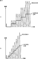
次に、図6は、プロジェクション装置11が、固定ピクセルクロックに同期して、レーザビームを照射する場合、スクリーン12上に輝度むらが生じるときの一例を示している。
Next, FIG. 6 shows an example in which uneven brightness occurs on the
図6Aにおいて、丸印(○)は、入力される映像信号の画素の位置を示しており、矩形(■)は、固定ピクセルクロックに生じる立ち上がりエッジのタイミングを示している。 In FIG. 6A, a circle (◯) indicates the position of the pixel of the input video signal, and a rectangle (■) indicates the timing of the rising edge generated in the fixed pixel clock.
図6Bには、プロジェクション装置11から照射されるレーザビームの光パワー(光強度)を示している。図6Bにおいて、横軸は時間を表し、縦軸は光パワーを表す。このことは、図7Aについても同様である。
FIG. 6B shows the optical power (light intensity) of the laser beam emitted from the
また、図6Bにおいて、固定ピクセルクロックに立ち上がりエッジが生じるタイミング、すなわち、画素としてレーザビームの照射が開始されるタイミングを、点線で示している。なお、時間12,14,16,18,20,22,24,26,28に対応する点線と区別するため、立ち上がりエッジが生じるタイミングを示す点線は、光パワー0.0から1.1まで延びた点線とされる。このことは、後述する図7Aについても同様である。
In FIG. 6B, the timing at which the rising edge occurs in the fixed pixel clock, that is, the timing at which the irradiation of the laser beam as the pixel is started is indicated by a dotted line. In order to distinguish from the dotted lines corresponding to the
図6Cには、スクリーン12上に投影される画素の輝度の一例を示している。図6Cにおいて、横軸は、スクリーン12の中央の位置を0.0としたときの水平方向の位置を表す。この位置は、スクリーン12の中央の位置からの距離[m]により表される。また、縦軸は輝度を表す。さらに、図6Cにおいて、画素の位置を、点線で示している。なお、図6Cにおいて、位置-0.2,-0.1,0.0,0.1,0.2,0.3に対応する点線と区別するため、画素の位置を示す点線は、輝度0から約170まで延びた点線とされる。このことは、図7B、図13B及び図17Bについても同様である。
FIG. 6C shows an example of the luminance of the pixels projected on the
例えば、プロジェクション装置11が、図6Bに示されるように、スクリーン12上の走査位置に拘らず、一定の光パワーでレーザビームを照射する場合を考える。この場合、スクリーン12に投影される画像の各画素の輝度は、図6Cに示されるように、スクリーン12の端近傍で輝度が急激に高くなる。これは、スクリーン12の端近傍で走査速度が遅くなるため、図6Aに示されるように、固定ピクセルクロックに同期して投影される画素の位置が密になることによる。
For example, consider a case where the
プロジェクション装置11では、図6Bに示したような一定の光パワーで、レーザビームを照射する場合、図6Cに示したように、スクリーン12の中央付近と端近傍とで輝度が異なるものとなり、輝度むらが生じてしまう。
In the
次に、図7は、プロジェクション装置11が、固定ピクセルクロックに同期して、レーザビームを照射する場合、レーザビームの光パワーを変化させることにより、スクリーン12上に生じる輝度むらを抑止するときの一例を示している。
Next, FIG. 7 shows a case where the
プロジェクション装置11は、固定ピクセルクロックに同期して、図7Aに示されるように、スクリーン12の端に近づく程、レーザビームの光パワーを低下させる。これにより、プロジェクション装置11は、図7Bに示されるように、画素を投影するスクリーン12上の走査位置に拘らず、同一の輝度とすることができるので、輝度むらを抑制できる。
The
しかしながら、レーザビームの光パワーを、図7Aに示されるようにして変化させる場合、輝度むらを抑制できるものの、例えば、走査位置に拘らず、同一の光パワーでレーザビームを照射する場合と比較して、複雑な制御を行うこととなる。よって、そのような複雑な制御を行うために、多くの有効ビット幅が使用され、投影画像の階調等を表現するための有効ビット幅が少なくなるため、投影画像の画質(例えば、解像度など)が低下してしまう。 However, when the optical power of the laser beam is changed as shown in FIG. 7A, the luminance unevenness can be suppressed, but, for example, compared with the case of irradiating the laser beam with the same optical power regardless of the scanning position. Therefore, complicated control is performed. Therefore, many effective bit widths are used to perform such complicated control, and the effective bit width for expressing the gradation of the projected image is reduced, so that the image quality of the projected image (for example, resolution, etc.) ) Will decrease.
また、走査位置が変化する毎に、レーザビームの光パワーを切り替えるスイッチングを行う必要があるため、消費電力が増加してしまう。特に、スクリーン12の端ほど、頻繁にスイッチングが行われ、電力の消費が激しいものとなる。
Moreover, since it is necessary to perform switching for switching the optical power of the laser beam every time the scanning position changes, the power consumption increases. In particular, the edge of the
さらに、プロジェクション装置11は、固定ピクセルクロックに同期してレーザビームを照射する場合、一定の周波数とされる固定ピクセルクロックの周波数成分による放射ノイズが増加する。したがって、例えば、プロジェクション装置11をEMI(Electro-Magnetic Interference)規格に適合させるために、放射ノイズを遮断するシールド部材等が必要となり、プロジェクション装置11の製造コストの増加や、筐体の大型化を招いてしまう。
Furthermore, when the
そこで、プロジェクション装置11は、スクリーン12上の走査位置に応じて、固定ピクセルクロックを調整し、調整後の固定ピクセルクロック(可変ピクセルクロック)に同期して、レーザビームを照射する。これにより、スクリーン12上に輝度むらが生じることを抑止するようにしている。
Therefore, the
次に、図8は、固定ピクセルクロックに立ち上がりエッジが生じるタイミングと、可変ピクセルクロックに立ち上がりエッジが生じるタイミングの一例を示している。 Next, FIG. 8 shows an example of the timing at which the rising edge occurs in the fixed pixel clock and the timing at which the rising edge occurs in the variable pixel clock.
図8Aにおいて、丸印は、外部からプロジェクション装置11に入力される映像信号の各画素の位置、つまり、映像信号規格に従った画素配列を示している。
In FIG. 8A, a circle indicates the position of each pixel of the video signal input to the
図8Bにおいて、矩形は、固定ピクセルクロックに立ち上がりエッジが生じるタイミングを示している。図8Bでは、スクリーン12の端ほど近接した状態で、画素が投影されることとなる。
In FIG. 8B, a rectangle indicates the timing at which a rising edge occurs in the fixed pixel clock. In FIG. 8B, pixels are projected in a state in which they are closer to the end of the
図8Cにおいて、矩形は、可変ピクセルクロックに立ち上がりエッジが生じるタイミングを示している。図8Cでは、スクリーン12上に一定の間隔で画素が投影されることとなる。
In FIG. 8C, a rectangle indicates the timing at which a rising edge occurs in the variable pixel clock. In FIG. 8C, pixels are projected on the
プロジェクション装置11は、レーザビームの走査位置に基づいて、例えば、図8Cに示されるようにして、一定の間隔で画素を投影できるように、固定ピクセルクロックを調整する。そして、プロジェクション装置11は、調整後の固定ピクセルクロック(可変ピクセルクロック)に同期して、レーザビームを照射することにより、一定の間隔で画素を投影する。これにより、スクリーン12上で輝度むらが生じることを抑止できる。
Based on the scanning position of the laser beam, the
[クロック生成部53の詳細]
次に、図9は、クロック生成部53の詳細な構成例を示している。
[Details of clock generator 53]
Next, FIG. 9 shows a detailed configuration example of the
クロック生成部53は、位相比較器151、ループフィルタ152、クロック調整回路153、及び出力選択回路154から構成される。
The
位相比較器151には、図2のスキャナ駆動回路37の制御回路134から、固定ピクセルクロックが供給される。位相比較器151は、制御回路134からの固定ピクセルクロックと、クロック調整回路153からフィードバックされる出力結果を比較し、その比較結果を、ループフィルタ152に供給する。
A fixed pixel clock is supplied to the
ループフィルタ152は、位相比較器151からの比較結果に対して、高域成分を除去するLPF(Low Pass Filter)処理を施し、LPF処理後の比較結果を、クロック調整回路153に供給する。
The
クロック調整回路153は、出力選択回路154からの、固定ピクセルクロックを調整するための出力選択情報に基づいて、固定ピクセルクロックを調整し、調整後の固定ピクセルクロックを、可変ピクセルクロックとして出力する。
The
すなわち、例えば、クロック調整回路153は、ループフィルタ152からの、LPF処理後の比較結果にしたがって、固定ピクセルクロックを遅延させる遅延量(遅延時間)を調整可能な9個のインバータ171乃至179及びスイッチ180から構成されるリングオシレータである。クロック調整回路153は、このような構成により、PLL(Phase Locked Loop)回路を構成することができる。つまり、リングオシレータとしてのクロック調整回路153は、固定ピクセルクロックと同じ周波数と位相により発振し、固定ピクセルクロックと同じ周波数と位相を有する波形OUT0(図10で後述)を出力する。
That is, for example, the
なお、クロック調整回路153において、インバータの個数は9個に限定されず、任意の奇数個とすることができる。また、クロック調整回路153としてのリングオシレータは、差動の回路構成とすることもできる。この場合、リングオシレータは、奇数個のインバータから構成する他、偶数個のインバータから構成することができる。
Note that in the
インバータ171乃至179は、ループフィルタ152からの、LPF処理後の比較結果に基づいて、図2のスキャナ駆動回路37の制御回路134から位相比較器151に供給される固定ピクセルクロックを、それぞれ決められた遅延量(遅延時間)だけ遅延させる。そして、インバータ171乃至179は、それぞれ決められた遅延量で遅延させた固定ピクセルクロックを出力する。
The
次に、図10は、インバータ171乃至179のそれぞれから出力される固定ピクセルクロックの波形OUT0乃至OUT8の一例を示している。
Next, FIG. 10 shows an example of waveforms OUT0 to OUT8 of the fixed pixel clock output from the
図10には、上から順に、インバータ179から出力される波形OUT0、インバータ171から出力される波形OUT1、インバータ172から出力される波形OUT2、インバータ173から出力される波形OUT3が示されている。さらに、図10には、インバータ174から出力される波形OUT4、インバータ175から出力される波形OUT5、インバータ176から出力される波形OUT6、インバータ177から出力される波形OUT7、インバータ178から出力される波形OUT8が示されている。なお、図10において、時刻tn-1から時刻tnまでの期間は、固定ピクセルクロックに立ち上がりエッジtn-1が生じたときから、次の立ち上がりエッジtnが生じるまでの期間を表す。
FIG. 10 shows, in order from the top, a waveform OUT0 output from the
波形OUT0は、固定ピクセルクロックと同一のタイミングで立ち上がりエッジを生じさせる波形である。波形OUT1は、固定ピクセルクロックの立ち上がりエッジから、遅延量d1だけ遅延したタイミングで立ち上がりエッジを生じさせる波形である。同様に、波形OUT2,OUT3,OUT4,OUT5,OUT6,OUT7,OUT8は、それぞれ、固定ピクセルクロックの立ち上がりエッジから、遅延量d2,d3,d4,d5,d6,d7,d8だけ遅延したタイミングで立ち上がりエッジを生じさせる波形である。 The waveform OUT0 is a waveform that generates a rising edge at the same timing as the fixed pixel clock. The waveform OUT1 is a waveform that generates a rising edge at a timing delayed by a delay amount d1 from the rising edge of the fixed pixel clock. Similarly, waveforms OUT2, OUT3, OUT4, OUT5, OUT6, OUT7, and OUT8 rise from the rising edge of the fixed pixel clock, respectively, with a delay of d2, d3, d4, d5, d6, d7, and d8. It is a waveform that causes an edge.
なお、図10において、遅延量d2=2×d1,d3=3×d1,d4=4×d1,d5=5×d1,d6=6×d1,d7=7×d1,d8=8×d1である。 In FIG. 10, the delay amount is d2 = 2 × d1, d3 = 3 × d1, d4 = 4 × d1, d5 = 5 × d1, d6 = 6 × d1, d7 = 7 × d1, d8 = 8 × d1. is there.
インバータ171は、インバータ179からの固定ピクセルクロックOUT0を、予め決められた遅延量(遅延時間)だけ遅延させ、遅延後の固定ピクセルクロックOUT1を、インバータ172及びスイッチ180に出力する。
The
同様にして、インバータ172は、インバータ171からの固定ピクセルクロックOUT1を、予め決められた遅延量だけ遅延させ、遅延後の固定ピクセルクロックOUT2を、インバータ173及びスイッチ180に出力する。インバータ173は、インバータ172からの固定ピクセルクロックOUT2を、予め決められた遅延量だけ遅延させ、遅延後の固定ピクセルクロックOUT3を、インバータ174及びスイッチ180に出力する。インバータ174は、インバータ173からの固定ピクセルクロックOUT3を、予め決められた遅延量だけ遅延させ、遅延後の固定ピクセルクロックOUT4を、インバータ175及びスイッチ180に出力する。インバータ175は、インバータ174からの固定ピクセルクロックOUT4を、予め決められた遅延量だけ遅延させ、遅延後の固定ピクセルクロックOUT5を、インバータ176及びスイッチ180に出力する。インバータ176は、インバータ175からの固定ピクセルクロックOUT5を、予め決められた遅延量だけ遅延させ、遅延後の固定ピクセルクロックOUT6を、インバータ177及びスイッチ180に出力する。インバータ177は、インバータ176からの固定ピクセルクロックOUT6を、予め決められた遅延量だけ遅延させ、遅延後の固定ピクセルクロックOUT7を、インバータ178及びスイッチ180に出力する。インバータ178は、インバータ177からの固定ピクセルクロックOUT7を、予め決められた遅延量だけ遅延させ、遅延後の固定ピクセルクロックOUT8を、インバータ179及びスイッチ180に出力する。
Similarly, the
インバータ179は、インバータ178からの固定ピクセルクロックOUT8を、予め決められた遅延量だけ遅延させ、遅延後の固定ピクセルクロックOUT0を、位相比較器151にフィードバック(供給)する。
The
また、インバータ179は、遅延後の固定ピクセルクロックOUT0を、スイッチ180とともに、出力選択回路154のカウンタ191、遅延量生成回路192、及びラッチ回路193に供給する。
The
図9に戻り、クロック調整回路153のスイッチ180は、出力選択回路154からの出力選択情報に基づいて、出力結果OUT0乃至OUT8のうち、出力選択情報に対応する遅延時間だけ遅延した出力結果を選択する。そして、スイッチ180は、選択した出力結果を、可変ピクセルクロックとして、図2の信号処理回路31のクロック生成部53に供給する。
Returning to FIG. 9, the
出力選択回路154は、図2のスキャナ駆動回路37の制御回路134からの水平同期信号と、クロック調整回路153からの固定ピクセルクロックOUT0に基づいて、スクリーン12上に走査されるレーザビームの位置を表す走査位置を算出する。そして、出力選択回路154は、算出した走査位置に基づいて、固定ピクセルクロックOUT0を調整するための出力選択情報を生成する。すなわち、例えば、出力選択回路154は、算出した走査位置に基づいて、固定ピクセルクロックOUT0を、走査位置に応じた遅延量だけ遅延させるための出力選択情報を生成する。
The
つまり、出力選択回路154は、カウンタ191、遅延量生成回路192及びラッチ回路193から構成される。
That is, the
カウンタ191は、図2のスキャナ駆動回路37の制御回路134から供給される水平同期信号の立ち上がりエッジを検出したとき、カウント数Cを0にリセットする。
When the
また、カウンタ191は、クロック調整回路153からの固定ピクセルクロックOUT0に基づいて、固定ピクセルクロックOUT0に立ち上がりエッジが生じたか否かを判定し、立ち上がりエッジが生じたと判定した場合、カウント数Cに1を加算(インクリメント)する。そして、カウンタ191は、加算後のカウント数Cを、遅延量生成回路192に出力する。なお、カウント数Cは、スクリーン12上の走査位置を表す。すなわち、例えば、カウント数C=1の場合、スクリーン12上の走査位置は、スクリーン12の端の位置とされる。
The
次に、図11は、カウンタ191が行う処理の一例を示している。
Next, FIG. 11 shows an example of processing performed by the
図11Aには、制御回路134から、クロック生成部53のカウンタ191に供給される水平同期信号の一例が示されている。この水平同期信号は、時刻t0において立ち上がりエッジt0を生じさせる。
FIG. 11A shows an example of a horizontal synchronization signal supplied from the control circuit 134 to the
図11Bには、クロック調整回路153からカウンタ191に供給される固定ピクセルクロックOUT0の一例が示されている。この固定ピクセルクロックOUT0は、時刻tn(n=0,1,…,13)毎に立ち上がりエッジtnを生じさせる。
FIG. 11B shows an example of the fixed pixel clock OUT0 supplied from the
図11Cには、クロック調整回路153から出力される可変ピクセルクロックの一例が示されている。この可変ピクセルクロックは、図11Bに示される固定ピクセルクロックOUT0の立ち上がりエッジを生じさせるタイミングを調整することにより生成され、立ち上がりエッジ0乃至8を生じさせる。
FIG. 11C shows an example of a variable pixel clock output from the
カウンタ191は、例えば、制御回路134からの水平同期信号(図11A)に生じた立ち上がりエッジを検出した場合、固定ピクセルクロックOUT0の立ち上がりエッジをカウントした回数を表すカウント数Cを0にリセットする。なお、カウンタ191は、カウント数Cを保持する内蔵の図示せぬメモリを有しているものとする。
For example, when the rising edge generated in the horizontal synchronizing signal (FIG. 11A) from the control circuit 134 is detected, the
また、カウンタ191は、クロック調整回路153からの固定ピクセルクロックOUT0(図11B)に生じる立ち上がりエッジtnを検出する毎に、カウント数Cを1だけ増加(インクリメント)させ、増加後のカウント数Cを、遅延量生成回路192に供給する。
The
すなわち、例えば、プロジェクション装置11では、水平同期信号の立ち上がりエッジt0が生じたときからのカウント数Cに基づいて、スクリーン12上の走査位置が判別され、その判別結果に基づいて、図11Cに示されるような可変ピクセルクロックが生成される。
That is, for example, in the
具体的には、例えば、時刻t0において、カウント数C=1となり、可変ピクセルクロックの立ち上がりエッジ0は、固定ピクセルクロックの立ち上がりエッジt0から遅延量d0だけ遅延したものとされる。なお、遅延量d0=0であるため、可変ピクセルクロックの立ち上がりエッジ0は、固定ピクセルクロックOUT0の立ち上がりエッジt0と同一のものとなる。
Specifically, for example, at time t0, the count number C = 1, and the rising
また例えば、時刻t1において、カウント数C=2となり、可変ピクセルクロックの立ち上がりエッジ1は、固定ピクセルクロックOUT0の立ち上がりエッジt1から遅延量d0(=0)だけ遅延したものとされる。さらに、例えば、時刻t2において、カウント数C=3となり、可変ピクセルクロックの立ち上がりエッジ2は、固定ピクセルクロックOUT0の立ち上がりエッジt2から遅延量d2だけ遅延したものとされる。同様にして、時刻t3において、カウント数C=4となり、可変ピクセルクロックの立ち上がりエッジ3は、固定ピクセルクロックOUT0の立ち上がりエッジt3から遅延量d4だけ遅延したものとされる。時刻t4において、カウント数C=5となる。そして、時刻t5において、カウント数C=6となり、可変ピクセルクロックの立ち上がりエッジ4は、固定ピクセルクロックOUT0の立ち上がりエッジt5から遅延量d0(=0)だけ遅延したものとされる。時刻t6において、カウント数C=7となり、可変ピクセルクロックの立ち上がりエッジ5は、固定ピクセルクロックOUT0の立ち上がりエッジt6から遅延量d6だけ遅延したものとされる。
For example, at time t1, the count number C = 2, and the rising
時刻t7において、カウント数C=8となる。そして、時刻t8において、カウント数C=9となり、可変ピクセルクロックの立ち上がりエッジ6は、固定ピクセルクロックOUT0の立ち上がりエッジt8から遅延量d4だけ遅延したものとされる。時刻t9において、カウント数C=10となる。そして、時刻t10において、カウント数C=11となり、可変ピクセルクロックの立ち上がりエッジ7は、固定ピクセルクロックOUT0の立ち上がりエッジt10から遅延量d4だけ遅延したものとされる。時刻t11において、カウント数C=12となる。そして、時刻t12において、カウント数C=13となり、可変ピクセルクロックの立ち上がりエッジ8は、固定ピクセルクロックOUT0の立ち上がりエッジt12から遅延量d6だけ遅延したものとされる。
At time t7, the count number C = 8. At time t8, the count number C = 9, and the rising
図9に戻り、遅延量生成回路192は、カウンタ191からのカウント数C、すなわち、スクリーン12上の走査位置に基づいて、固定ピクセルクロックOUT0の立ち上がりエッジを調整させるための出力選択情報を生成し、ラッチ回路193に供給する。
Returning to FIG. 9, the delay
すなわち、例えば、遅延量生成回路192は、RAM192aを内蔵しており、RAM192aは、カウント数Cと、遅延量dを表す出力選択情報を対応付けたテーブル(対応表)を保持している。
That is, for example, the delay
次に、図12は、RAM192aに保持されるテーブルの一例を示している。
Next, FIG. 12 shows an example of a table held in the
図12には、カウント数C、固定ピクセルクロックtn、遅延量dを表す出力選択情報、及び、固定ピクセルクロックtnを遅延量dだけ遅延させて得られる可変ピクセルクロックが対応付けられたテーブルの一例が示されている。 FIG. 12 shows an example of a table in which count number C, fixed pixel clock tn, output selection information indicating delay amount d, and variable pixel clock obtained by delaying fixed pixel clock tn by delay amount d are associated. It is shown.
なお、図12では、説明の便宜上、カウント数C、固定ピクセルクロックtn、出力選択情報、及び可変ピクセルクロックを示しているが、RAM192aには、例えば、カウント数Cと出力情報が対応付けられたテーブルが保持される。
In FIG. 12, for convenience of explanation, the count number C, the fixed pixel clock tn, the output selection information, and the variable pixel clock are shown, but the
遅延量生成回路192は、カウンタ191からのカウント数Cに基づいて、RAM192aに保持されているテーブルから、カウント数Cに対応付けられた出力選択情報を読み出し、ラッチ回路193に供給する。
Based on the count number C from the
図9に戻り、ラッチ回路193は、遅延量生成回路192からの出力選択情報をラッチして、クロック調整回路153のスイッチ180に出力する。
Returning to FIG. 9, the
[可変ピクセルクロックを用いるときの一例]
次に、図13は、プロジェクション装置11が、調整後の固定ピクセルクロック、すなわち、可変ピクセルクロックに同期して、固定の光パワーで、レーザビームを間欠的に照射するときの一例を示している。
[Example when using variable pixel clock]
Next, FIG. 13 shows an example when the
なお、図13Aにおいて、可変ピクセルクロックに立ち上がりエッジが生じるタイミングを、点線で示している。なお、時間12,14,16,18,20,22,24,26,28に対応する点線と区別するため、可変ピクセルの立ち上がりエッジが生じるタイミングを示す点線は、光パワー0.0から1.1まで延びた点線とされる。このことは、後述する図17Aについても同様である。
In FIG. 13A, the timing at which the rising edge occurs in the variable pixel clock is indicated by a dotted line. In order to distinguish from the dotted lines corresponding to
レーザ制御部54は、クロック生成部53からの可変ピクセルクロックに同期して、レーザ駆動回路32を制御することにより、図13Aに示されるように、スクリーン12の端に近づく程、時間の間隔を置いて、レーザビームを照射させる。すなわち、レーザ駆動回路32は、そのようなレーザビームを、レーザ制御部54からの制御に従い、光源部33を駆動させることにより照射させる。これにより、プロジェクション装置11は、スクリーン12上に一定の間隔で画素としてのレーザビームを照射することができる。
The
また、レーザ制御部54は、クロック生成部53からの可変ピクセルクロックに同期して、レーザ駆動回路32を制御することにより、図13Aに示されるように、スクリーン12に投影される画素毎に、レーザビームの光パワーの総和(=光パワー×照射時間)が同一となるように、レーザビームの走査位置に拘らず、固定の光パワーと照射時間で、レーザビームを照射させる。すなわち、レーザ駆動回路32は、そのようなレーザビームを、レーザ制御部54からの制御に従い、光源部33を駆動させることにより照射させる。
Further, the
これにより、プロジェクション装置11は、図13Bに示されるように、スクリーン12上の走査位置に拘らず、同一の輝度とすることができるので、輝度むらを抑制できる。
As a result, as shown in FIG. 13B, the
プロジェクション装置11は、可変ピクセルクロックに同期して、図13Aに示されるように、同一(固定)の光パワーでレーザビームを照射する。このため、例えば、図7Aに示されるようにして光パワーを変化させる場合のように、有効ビット幅が大幅に使用される事態を防止できる。よって、有効ビット幅を、投影画像の階調等を表すビットとして使用できるので、投影画像の画質の低下を防止できる。
The
また、プロジェクション装置11は、図13Aに示されるようにして、スクリーン12上に一定の間隔で画素としてのレーザビームを照射する場合、図7Aの場合と比較して、スクリーン12の端近傍におけるレーザビームの光パワーを切り替えるスイッチングを行う回数が少なくなるので、消費電力を抑制することができる。
Further, as shown in FIG. 13A, the
さらに、プロジェクション装置11は、可変ピクセルクロックに同期してレーザビームを照射する場合、可変ピクセルクロックは、固定ピクセルクロックとは異なり、周波数成分がより広い帯域に分散しているため、放射ノイズのピークを抑制できる。このため、放射ノイズを遮断するシールド部材等が不要となり、プロジェクション装置11の製造コストの増加や、筐体の大型化を防止できる。
Further, when the
また、プロジェクション装置11は、図13Aに示したようにして、レーザビームを間欠的に照射するようにした。このため、プロジェクション装置11において、レーザビームを照射するために必要な閾値電流分の寄与を半減させることができる。
Further, the
次に、図14は、レーザビームを間欠的に照射する場合、連続して照射する場合と比較して、閾値電流分の寄与を半減できることを示している。 Next, FIG. 14 shows that when the laser beam is irradiated intermittently, the contribution of the threshold current can be halved compared to the case of continuous irradiation.
レーザ光源91B,91G,91Rは、それぞれ、閾値電流Ith以上のレーザ駆動電流Iが供給された場合、発光寄与分の電流(I-Ith)に応じた光パワーでレーザビームを出射する。 Each of the laser light sources 91B, 91G, and 91R emits a laser beam with optical power corresponding to the current (II th ) corresponding to the light emission contribution when the laser drive current I equal to or greater than the threshold current Ith is supplied.
すなわち、図14Aには、レーザ光源91B,91G,91Rが、レーザ駆動電流I=I1に基づいて、レーザビームを連続して照射するときの一例を示している。 That is, FIG. 14A shows an example when the laser light sources 91B, 91G, and 91R continuously irradiate a laser beam based on the laser driving current I = I 1 .
図14Bには、レーザ光源91B,91G,91Rが、レーザ駆動電流I=I2に基づいて、レーザビームを間欠的に照射するときの一例を示している。なお、電流I2>I1であるものとする。 FIG. 14B shows an example when the laser light sources 91B, 91G, and 91R irradiate the laser beam intermittently based on the laser drive current I = I 2 . It is assumed that current I 2 > I 1 .
プロジェクション装置11において、図14Bに示されるように、レーザビームを間欠的に照射する場合、図14Aに示されるように連続して照射する場合と比較して、同一の発光寄与分を維持したまま、閾値電流分の寄与を半減できる。
In the
よって、プロジェクション装置11において、レーザビームを間欠的に照射する場合、発光寄与分を維持したまま、閾値電流の消費電力を抑制することが可能となる。
Therefore, when the
[プロジェクション装置11の動作説明]
次に、図15のフローチャートを参照して、プロジェクション装置11が行う投影処理を説明する。
[Description of Operation of Projection Device 11]
Next, the projection processing performed by the
この投影処理は、例えば、プロジェクション装置11に、外部から映像信号が供給されたときに開始される。
This projection processing is started, for example, when a video signal is supplied to the
ステップS1において、信号処理回路31のビデオデコーダ51は、外部からの映像信号を、光源部33の各光源の波長に応じた色域の映像に色域変換し、色域変換後の映像信号を、フレームメモリ52に供給して保持させる。なお、フレームメモリ52は、後述するステップS4のクロック調整処理により得られる、クロック生成部53からの可変ピクセルクロックに同期して、保持している色域変換後の映像信号をレーザ制御部54に供給する。
In step S <b> 1, the
ステップS2において、スキャナ駆動回路37は、スキャナ部36に内蔵の図示せぬ角度センサからの水平角度信号に基づいて、水平駆動信号を生成し、スキャナ部36に供給する。また、スキャナ駆動回路37は、スキャナ部36に内蔵の図示せぬ角度センサからの垂直角度信号に基づいて、垂直駆動信号を生成し、スキャナ部36に供給する。
In step S <b> 2, the scanner drive circuit 37 generates a horizontal drive signal based on a horizontal angle signal from an angle sensor (not shown) built in the
そして、スキャナ部36は、スキャナ駆動回路37からの水平駆動信号及び垂直駆動信号に基づいて、光源部33からのレーザビームがスクリーン12の水平方向及び垂直方向にスキャン(走査)されるように、内蔵の駆動ミラー111を駆動する。これにより、レーザビームは、駆動ミラー111に反射してスクリーン12上に照射される。なお、レーザビームの照射は、後述するステップS7の処理で行われる。
The
また、スキャナ部36において、内蔵の図示せぬ角度センサは、駆動ミラー111の水平角度と垂直角度を検出し、それぞれ、水平角度信号と垂直角度信号としてスキャナ駆動回路37に供給する。
In the
ステップS3において、スキャナ駆動回路37は、スキャナ部36が内蔵する図示せぬ角度センサからの水平角度信号に基づいて、水平同期信号及び固定ピクセルクロックを生成して、信号処理回路31のクロック生成部53に供給する。さらに、スキャナ駆動回路37は、スキャナ部36が内蔵する図示せぬ角度センサからの垂直角度信号に基づいて、垂直同期信号を生成して、信号処理回路31のクロック生成部53に供給する。
In step S3, the scanner driving circuit 37 generates a horizontal synchronization signal and a fixed pixel clock based on a horizontal angle signal from an angle sensor (not shown) built in the
ステップS4において、クロック生成部53は、固定ピクセルクロックを調整するクロック調整処理を行う。そして、クロック生成部53は、クロック調整処理により調整後の固定ピクセルクロックを、可変ピクセルクロックとして、フレームメモリ52及びレーザ制御部54に供給する。
In step S4, the
なお、ステップS4におけるクロック調整処理は、ステップS5以降も継続して行われる。クロック調整処理の詳細は、図16を参照して後述する。 Note that the clock adjustment processing in step S4 is continuously performed after step S5. Details of the clock adjustment processing will be described later with reference to FIG.
ステップS5において、レーザ制御部54は、クロック生成部53からの可変ピクセルクロックに同期して、レーザ駆動回路32を制御することにより、スクリーン12上にレーザビームを画素として照射させる。
In step S <b> 5, the
すなわち、例えば、レーザ制御部54は、クロック生成部53からの可変ピクセルクロックに同期して、受光素子35から取得したレーザパワーモニタ信号に基づき色毎に生成した投影映像信号を、クロック生成部53からの可変ピクセルクロック、及び映像電流制御信号とともに、レーザ駆動回路32に供給する。
That is, for example, the
なお、レーザ制御部54は、クロック生成部53からの垂直同期信号に同期して、レーザ駆動回路32を制御することにより、帰線区間におけるレーザビームの照射を行わないようにする。
The
ステップS6において、レーザ駆動回路32のレーザ駆動部71B,71G,71Rは、それぞれ、レーザ制御部54からの制御に従い、レーザ駆動電流を生成し、光源部33のレーザ光源91B,91G,91Rに供給する。具体的には、レーザ駆動部71B,71G,71Rは、それぞれ、レーザ制御部54からの可変ピクセルクロックに同期して、同じくレーザ制御部54から供給される投影映像信号を用いて、色毎のレーザ駆動電流を生成し、レーザ光源91B,91G,91Rに供給する。レーザ駆動部71B,71G,71Rから、それぞれ、色毎のレーザ駆動電流が供給されることにより、レーザ光源91B,91G,91Rは駆動される。
In step S6, the
ステップS7において、レーザ光源91B,91G,91Rは、それぞれ、レーザ駆動部71B,71G,71Rからのレーザ駆動電流に基づいて、レーザビームを照射する。これらのレーザビームは、1本のレーザビームとして、ビームスプリッタ34を透過し、駆動ミラー111に照射される。
In step S7, the laser light sources 91B, 91G, and 91R irradiate laser beams based on the laser drive currents from the
また、レーザ光源91B,91G,91Rから照射されるレーザビームの一部は、ビームスプリッタ34により、受光素子35の方向に反射される。これにより、受光素子35は、ビームスプリッタ34からのレーザビームの光を受光することにより、光源部33の各レーザ光源91B,91G,91Rの光出力(光パワー)を検出し、それらの検出結果を、レーザパワーモニタ信号として、信号処理回路31のレーザ制御部54に供給する。
A part of the laser beam emitted from the laser light sources 91B, 91G, and 91R is reflected by the
ステップS8において、システム制御部55は、図示せぬ操作部からの操作信号に基づいて、投影処理の中止を指示する中止操作が行われたか否かを判定し、中止操作が行われていないと判定した場合、処理をステップS1に戻し、それ以降同様の処理が行われる。
In step S8, the
また、ステップS8において、システム制御部55は、図示せぬ操作部からの操作信号に基づいて、中止操作が行われたと判定した場合、投影処理を終了させる。
In step S8, when the
[クロック調整処理の詳細]
次に、図16のフローチャートを参照して、図15のステップS4におけるクロック調整処理の詳細について説明する。
[Details of clock adjustment processing]
Next, details of the clock adjustment processing in step S4 of FIG. 15 will be described with reference to the flowchart of FIG.
ステップS21では、位相比較器151は、制御回路134からの固定ピクセルクロックと、クロック調整回路153からフィードバックされる出力結果を比較し、その比較結果を、ループフィルタ152に供給する。
In
ステップS22では、ループフィルタ152は、位相比較器151からの比較結果に対して、高域成分を除去するLPF処理を施し、LPF処理後の比較結果を、クロック調整回路153に出力する。
In step S <b> 22, the
ステップS23では、クロック調整回路153は、出力選択回路154からの出力選択情報に基づいて、固定ピクセルクロックを調整し、調整後の固定ピクセルクロックを、可変ピクセルクロックとして、図2のフレームメモリ52及びレーザ制御部54に出力する。なお、後述するステップS26において、出力選択回路154のラッチ回路193からクロック調整回路153に対して、出力選択情報が供給される。
In step S23, the
ステップS24では、出力選択回路154において、カウンタ191は、クロック調整回路153からの固定ピクセルクロックに基づいて、固定ピクセルクロックに立ち上がりエッジが生じたか否かを判定し、立ち上がりエッジが生じたと判定した場合、カウント数Cに1を加算(インクリメント)する。そして、カウンタ191は、加算後のカウント数Cを、遅延量生成回路192に出力する。なお、カウント数Cは、スクリーン12上の走査位置を表す。
In step S24, in the
なお、カウンタ191は、図2のスキャナ駆動回路37の制御回路134から供給される水平同期信号の立ち上がりエッジを検出したとき、カウント数Cを0にリセットする。
The
ステップS25では、遅延量生成回路192は、カウンタ191からのカウント数Cに基づいて、RAM192aに保持されているテーブルから、複数の異なる出力選択情報のうち、カウント数Cに対応付けられた出力選択情報を読み出し、ラッチ回路193に供給する。
In step S25, the delay
ステップS26では、ラッチ回路193は、遅延量生成回路192からの出力選択情報をラッチして、クロック調整回路153のスイッチ180に供給し、処理をステップS23に戻して、それ以降同様の処理が繰り返される。
In step S26, the
以上説明したように、クロック調整処理によれば、クロック調整回路153は、走査位置に基づいて、固定ピクセルクロックを調整することにより可変ピクセルクロックを生成するようにした。そして、レーザ制御部54は、クロック調整回路153からの可変ピクセルクロックに同期して、レーザビームの照射を制御するようにした。
As described above, according to the clock adjustment process, the
このため、プロジェクション装置11では、画質の劣化や、消費電力、放射ノイズ等を抑制しつつ、輝度むらを抑制することが可能となる。
For this reason, the
<2.変形例>
本実施の形態では、プロジェクション装置11は、図13Aに示されるように、同一の光パワーと照射時間で、間欠的にレーザビームを照射するようにしたが、レーザビームの照射方法は、これに限定されない。
<2. Modification>
In the present embodiment, as shown in FIG. 13A, the
次に、図17は、プロジェクション装置11が、可変ピクセルクロックに同期して、走査位置に応じて異なる光パワーと照射時間で、レーザビームを間欠的に照射するときの一例を示している。
Next, FIG. 17 shows an example when the
図17Aには、可変ピクセルクロックにおいて、各画素毎に、画素を投影する際の照射時間のデューティ比を一定としたときの一例が示されている。 FIG. 17A shows an example when the duty ratio of the irradiation time when projecting a pixel is constant for each pixel in the variable pixel clock.
ここで、デューティ比とは、例えば、可変ピクセルクロックに立ち上がりエッジxが生じたときから、次の立ち上がりエッジx+1が生じるまでの画素期間における照射時間(立ち上がりエッジ0が生じるタイミングに同期して画素を投影する際の照射時間)の比を表す。デューティ比は、レーザビームの走査位置に拘らず、投影される画素毎に同一とされる。
Here, the duty ratio is, for example, the irradiation time in the pixel period from when the rising edge x occurs in the variable pixel clock to when the next rising edge x + 1 occurs (the pixel is synchronized with the timing when the rising
図17Aでは、各画素期間において、異なる照射時間でレーザビームを照射するものの、投影される画素としてのレーザビームの光パワーの総和が同一となるように、光パワーが異なるものとされる。 In FIG. 17A, in each pixel period, the laser beam is irradiated at different irradiation times, but the optical powers are different so that the sum of the optical powers of the laser beams as the projected pixels is the same.
すなわち、例えば、レーザ制御部54は、クロック生成部53からの可変ピクセルクロックに同期して、レーザ駆動回路32を制御することにより、図17Aに示されるように、スクリーン12の端ほど、低い光パワーでレーザビームを照射させる。
That is, for example, the
より具体的には、レーザ制御部54は、クロック生成部53からの可変ピクセルクロックに同期して、レーザ駆動回路32を制御することにより、レーザビームの走査位置毎に異なる光パワーと照射時間で、レーザビームを照射させる。すなわち、レーザ駆動回路32は、そのようなレーザビームを、レーザ制御部54からの制御に従い、光源部33を駆動させることにより照射させる。
More specifically, the
なお、いずれの画素においても、画素期間において照射されるレーザビームの光パワーの総和(=光パワー×照射時間)は同一とされるので、図17Bに示されるように、いずれの位置においても輝度は同一とされ、輝度むらを防止できる。 In any pixel, since the total light power (= light power × irradiation time) of the laser beam irradiated in the pixel period is the same, as shown in FIG. Are the same, and uneven brightness can be prevented.
また、図17Aにおいて、図13Aの場合と同様に、スクリーン12の端に近づく程、時間の間隔を置いて、レーザビームを照射させているので、スクリーン12上に一定の間隔で画素としてのレーザビームを照射することができる。
Further, in FIG. 17A, as in the case of FIG. 13A, the laser beam is irradiated at a time interval as the end of the
ところで、プロジェクション装置11では、画素の寸法に相当する小さなスポット光をスクリーン12上に形成するために、比較的、波長のスペクトラム幅が狭く位相が揃った光(コヒーレンスの高い光)であるレーザビームの照射を行うようにしている。
By the way, in the
このため、プロジェクション装置11においては、スクリーン12上の微小な凹凸に起因する、スペックルノイズと呼ばれる斑点の模様が、スクリーン12上の投影画像を視認する視認者の網膜上に発生してしまう。
For this reason, in the
よって、プロジェクション装置11では、レーザ光源91B,91G,91Rのそれぞれから出射されるレーザビームのスペクトラム幅をより広くして、すなわち、レーザビームをコヒーレンスの低い光にして、スペックルノイズを低減させるようにしてもよい。
Therefore, in the
次に、図18は、レーザビームをコヒーレンスの低い光にするための処理の一例を示している。 Next, FIG. 18 shows an example of a process for making a laser beam light with low coherence.
図18Aには、投影映像信号と、投影映像信号に重畳される高周波信号の一例が示されている。図18Aに示される投影映像信号と高周波信号は、投影画像の解像度が比較的低く、投影映像信号及び可変ピクセルクロックの周波数が比較的低い場合のものである。図18Aにおける場合、高周波信号の周波数は、投影映像信号及び可変ピクセルクロックの周波数よりも高いものとなっている。 FIG. 18A shows an example of a projection video signal and a high-frequency signal superimposed on the projection video signal. The projection video signal and the high frequency signal shown in FIG. 18A are those when the resolution of the projection image is relatively low and the frequencies of the projection video signal and the variable pixel clock are relatively low. In the case of FIG. 18A, the frequency of the high-frequency signal is higher than the frequencies of the projection video signal and the variable pixel clock.
図18Bには、投影映像信号と、投影映像信号に重畳される高周波信号の他の一例が示されている。図18Bに示される投影映像信号と高周波信号は、投影画像の解像度が比較的高く、投影映像信号及び可変ピクセルクロックの周波数が比較的高い場合のものである。図18Bにおける場合、高周波信号の周波数は、投影映像信号及び可変ピクセルクロックの周波数と同じ周波数となっている。 FIG. 18B shows another example of the projection video signal and the high-frequency signal superimposed on the projection video signal. The projection video signal and the high frequency signal shown in FIG. 18B are those when the resolution of the projection image is relatively high and the frequencies of the projection video signal and the variable pixel clock are relatively high. In the case of FIG. 18B, the frequency of the high-frequency signal is the same as the frequency of the projection video signal and the variable pixel clock.
レーザ駆動部71R,71G,71Bは、それぞれ、レーザ制御部54からの投影映像信号に高周波信号を重畳し、重畳後の投影映像信号に基づいて、レーザ駆動電流を生成し、レーザ光源91R,91G,91Bに供給する。なお、レーザ駆動電流は、例えば、重畳後の投影映像信号を、レーザ光源91R,91G,91Bの駆動に必要な電流値まで増幅することにより生成される。
The
レーザ光源91R,91G,91Bは、それぞれ、高周波信号を投影映像信号に重畳して得られたレーザ駆動電流に基づいて、コヒーレンスの低いレーザビームを出射することとなる。 Each of the laser light sources 91R, 91G, and 91B emits a laser beam with low coherence based on a laser drive current obtained by superimposing a high-frequency signal on a projection video signal.
なお、図18A及び図18Bに示されるように、高周波信号を重畳してレーザ駆動電流を生成する場合、そのようなレーザ駆動電流の振幅は、高周波信号を重畳しない場合と比較して大きくなるため、放射ノイズが発生し易くなってしまう。 As shown in FIGS. 18A and 18B, when a laser drive current is generated by superimposing a high-frequency signal, the amplitude of such a laser drive current is larger than when no high-frequency signal is superimposed. Radiation noise is likely to occur.
この場合、例えば、プロジェクション装置11は、図17Aに示されるように、レーザビームの照射のタイミングのみならず、画素として照射されるレーザビームの照射時間も、走査位置に応じて変化させることが望ましい。
In this case, for example, as shown in FIG. 17A, the
すなわち、例えば、プロジェクション装置11は、周波数成分がより広い帯域に分散された可変ピクセルクロックに同期して、レーザビームの照射を行うことにより、放射ノイズのピークを低減させることが望ましい。これにより、例えば、シールド部材等を用いることなく、プロジェクション装置11を、EMI規格に適合させることができる。
That is, for example, it is desirable that the
なお、本実施の形態では、プロジェクション装置11は、赤色、緑色及び青色の各レーザビームを照射するようにしたが、赤色、緑色及び青色の各レーザビームとともに、新たに他のレーザビーム(例えば、赤色のレーザビーム等)も照射することができる。
In the present embodiment, the
この場合、光源部33には、他のレーザビームを照射するためのレーザ光源、コリメートレンズ、及びダイクロイックミラーが、レーザ駆動回路32には、他のレーザビームを照射するためのレーザ光源を駆動させるレーザ駆動部が新たに設けられる。
In this case, the light source unit 33 has a laser light source, a collimating lens, and a dichroic mirror for irradiating other laser beams, and the
また、本実施の形態では、スクリーン12上に画像を投影するプロジェクション装置11について説明したが、本技術は、画像を投影する機能を有する、スマートフォンやパーソナルコンピュータ等の電子機器にも適用できる。
Moreover, although this Embodiment demonstrated the
すなわち、例えば、固定ピクセルクロックを可変ピクセルクロックに調整し、可変ピクセルクロックに同期して、レーザビームの制御を行うレーザ制御部54、及びレーザ制御部54からの制御に従って光源部33を駆動するレーザ駆動回路32を内蔵する電子機器であれば、どのような電子機器にも、本技術を適用できる。
That is, for example, a fixed pixel clock is adjusted to a variable pixel clock, a
その他、例えば、本技術は、可変ピクセルクロックに同期して、レーザビームの制御を行う制御装置に適用することができる。この制御装置は、固定ピクセルクロックを可変ピクセルクロックに調整するクロック生成部53と、クロック生成部53からの可変ピクセルクロックに同期して、レーザビームを画素として照射させるレーザ制御部54から構成される。
In addition, for example, the present technology can be applied to a control device that controls a laser beam in synchronization with a variable pixel clock. The control device includes a
さらに、本技術は、可変ピクセルクロックに同期して、レーザビームを照射する光源部33を駆動させる駆動装置に適用することができる。この駆動装置は、固定ピクセルクロックを可変ピクセルクロックに調整するクロック生成部53と、クロック生成部53からの可変ピクセルクロックに同期して生成したレーザ駆動電流に基づいて、光源部33を駆動させるレーザ駆動回路32から構成される。
Furthermore, the present technology can be applied to a driving device that drives the light source unit 33 that emits a laser beam in synchronization with the variable pixel clock. The driving device includes a
なお、図9のクロック調整回路153は、一定の周期で立ち上がりエッジを生じさせる固定ピクセルクロックを可変ピクセルクロックに調整するようにしたが、調整の対象は、これに限定されない。
Note that the
すなわち、調整の対象は、スクリーン上で走査されるレーザビームの照射のタイミングを表すクロックであればどのようなクロックでもよく、必ずしも、一定の周期で立ち上がりエッジを生じさせる固定ピクセルクロックである必要はない。 In other words, the adjustment target may be any clock as long as it represents the irradiation timing of the laser beam scanned on the screen, and is not necessarily a fixed pixel clock that generates a rising edge at a constant period. Absent.
また、本実施の形態では、図9のクロック生成部53は、スクリーン12上の走査位置に基づいて、固定ピクセルクロックの立ち上がりエッジを遅延させることにより可変ピクセルクロックを生成するようにした。しかしながら、可変ピクセルクロックの生成方法は、これに限定されない。
In this embodiment, the
すなわち、例えば、クロック生成部53は、固定ピクセルクロックの立ち上がりエッジを進めることにより可変ピクセルクロックを生成するようにしてもよい。
That is, for example, the
上述した一連の処理は、例えばハードウェアにより実行することもできるし、ソフトウェアにより実行することもできる。一連の処理をソフトウェアにより実行する場合には、そのソフトウェアを構成するプログラムが、専用のハードウェアに組み込まれているコンピュータ、又は、各種のプログラムをインストールすることで、各種の機能を実行することが可能な、例えば汎用のコンピュータなどに、プログラム記録媒体からインストールされる。 The series of processes described above can be executed by hardware or software, for example. When a series of processing is executed by software, a program constituting the software may execute various functions by installing a computer incorporated in dedicated hardware or various programs. For example, it is installed from a program recording medium in a general-purpose computer or the like.
[コンピュータの構成例]
図19は、上述した一連の処理をプログラムにより実行するコンピュータの構成例を示している。
[Computer configuration example]
FIG. 19 shows a configuration example of a computer that executes the above-described series of processing by a program.
CPU301は、ROM(Read Only Memory)302、又は記憶部308に記憶されているプログラムに従って各種の処理を実行する。RAM303には、CPU301が実行するプログラムやデータ等が適宜記憶される。これらのCPU301、ROM303、及びRAM303は、バス304により相互に接続されている。
The
CPU301にはまた、バス304を介して入出力インタフェース305が接続されている。入出力インタフェース305には、キーボード、マウス、マイクロホン等よりなる入力部306、ディスプレイ、スピーカ等よりなる出力部307が接続されている。CPU301は、入力部306から入力される指令に対応して各種の処理を実行する。そして、CPU301は、処理の結果を出力部307に出力する。
An input /
入出力インタフェース305に接続されている記憶部308は、例えばハードディスクからなり、CPU301が実行するプログラムや各種のデータを記憶する。通信部309は、インタネットやローカルエリアネットワーク等のネットワークを介して外部の装置と通信する。
The
また、通信部309を介してプログラムを取得し、記憶部308に記憶してもよい。
A program may be acquired via the
入出力インタフェース305に接続されているドライブ310は、磁気ディスク、光ディスク、光磁気ディスク、或いは半導体メモリ等のリムーバブルメディア311が装着されたとき、それらを駆動し、そこに記録されているプログラムやデータ等を取得する。取得されたプログラムやデータは、必要に応じて記憶部308に転送され、記憶される。
The drive 310 connected to the input /
コンピュータにインストールされ、コンピュータによって実行可能な状態とされるプログラムを記録(記憶)する記録媒体は、図19に示すように、磁気ディスク(フレキシブルディスクを含む)、光ディスク(CD-ROM(Compact Disc-Read Only Memory),DVD(Digital Versatile Disc)を含む)、光磁気ディスク(MD(Mini-Disc)を含む)、もしくは半導体メモリ等よりなるパッケージメディアであるリムーバブルメディア311、又は、プログラムが一時的もしくは永続的に格納されるROM302や、記憶部308を構成するハードディスク等により構成される。記録媒体へのプログラムの記録は、必要に応じてルータ、モデム等のインタフェースである通信部309を介して、ローカルエリアネットワーク、インタネット、デジタル衛星放送といった、有線又は無線の通信媒体を利用して行われる。
As shown in FIG. 19, a recording medium for recording (storing) a program installed in a computer and ready to be executed by the computer includes a magnetic disk (including a flexible disk), an optical disk (CD-ROM (Compact Disc-
なお、本明細書において、上述した一連の処理を記述するステップは、記載された順序に沿って時系列的に行われる処理はもちろん、必ずしも時系列的に処理されなくとも、並列的あるいは個別に実行される処理をも含むものである。 In the present specification, the steps describing the series of processes described above are not limited to the processes performed in time series according to the described order, but are not necessarily performed in time series, either in parallel or individually. The process to be executed is also included.
さらに、本開示は、上述した実施の形態に限定されるものではなく、本開示の要旨を逸脱しない範囲において種々の変更が可能である。 Furthermore, the present disclosure is not limited to the above-described embodiments, and various modifications can be made without departing from the gist of the present disclosure.
11 プロジェクション装置, 12 スクリーン, 31 信号処理回路, 32 レーザ駆動回路, 33 光源部, 34 ビームスプリッタ, 35 受光素子, 36 スキャナ部, 37 スキャナ駆動回路, 51 ビデオデコーダ, 52 フレームメモリ, 53 クロック生成部, 54 レーザ制御部, 55 システム制御部, 71R,71G,71B レーザ駆動部, 91R,91G,91B レーザ光源, 92R,92G,92B コリメートレンズ, 93R,93G,93B ダイクロイックミラー, 111 駆動ミラー, 131 制御回路, 132 バッファ, 133 駆動回路, 134 制御回路, 135 駆動回路, 135 バッファ, 151 位相比較器, 152 ループフィルタ, 153 クロック調整回路, 154 出力選択回路, 171乃至179 インバータ, 180 スイッチ, 191 カウンタ, 192 遅延量生成回路, 192a RAM, 193 ラッチ回路
DESCRIPTION OF
Claims (12)
前記レーザビームを共振周波数に従って所定の方向に角度を変化させながら反射してスクリーン上に走査させる反射部と、
前記反射部により前記スクリーン上で走査される前記レーザビームの照射のタイミングを表す固定ピクセルクロックからなる第1のクロックを走査位置に応じた遅延時間だけ遅延させることで調整するための調整用情報を、前記レーザビームが走査される走査位置に基づいて生成する生成部と、
前記調整用情報に基づいて、前記第1のクロックを、前記遅延時間だけ遅延させた第2のクロックに調整する調整部と、
前記第2のクロックに同期して、前記レーザビームを画素として間欠的に照射させるレーザ制御部とを含み、
前記レーザ制御部は、前記第2のクロックに同期して、前記スクリーンに投影される画素毎に、前記レーザビームの光パワーの総和が同一となるように、前記走査位置毎に異なる光パワーと照射時間で、前記レーザビームを照射させる
制御装置。 A light source unit for irradiating a laser beam;
A reflection unit that reflects the laser beam while changing an angle in a predetermined direction according to a resonance frequency and scans the laser beam on a screen;
Adjustment information for adjusting by delaying a first clock composed of a fixed pixel clock representing the irradiation timing of the laser beam scanned on the screen by the reflection unit by a delay time corresponding to a scanning position. A generator that generates a laser beam based on a scanning position scanned by the laser beam;
An adjusting unit that adjusts the first clock to a second clock delayed by the delay time based on the adjustment information;
A laser controller that intermittently irradiates the laser beam as a pixel in synchronization with the second clock ;
The laser control unit synchronizes with the second clock and outputs different optical power for each scanning position so that the total optical power of the laser beam is the same for each pixel projected on the screen. A control device for irradiating the laser beam with an irradiation time .
請求項1に記載の制御装置。 Since the rising edge in the second clock has occurred, then the ratio of the irradiation time in the pixel period until the rising edge occurs, the control device according to claim 1 which is irrespective identical to the scanning position .
請求項1または2に記載の制御装置。 The laser control unit, the second in synchronization with the clock, the control device according to claim 1 or 2 is irradiated with the laser beam as a pixel at regular intervals on the screen.
前記第1のクロックを、それぞれ異なる遅延時間だけ遅延させるタイミング遅延部と、
前記調整用情報に基づいて、それぞれ異なる遅延時間だけ遅延された複数の前記第1のクロックのいずれかを、前記第2のクロックとして選択する選択部と
を有する請求項1乃至3のいずれかに記載の制御装置。 The adjustment unit is
A timing delay unit for delaying the first clock by different delay times;
Based on the adjustment information, one of a plurality of said delayed by different delay times each of the first clock, to any one of claims 1 to 3 and a selection unit for selecting as said second clock The control device described.
前記第1のクロックに基づいて、前記走査位置を算出する位置算出部と、
予め保持している複数の異なる調整用情報の中から、算出された前記走査位置に応じた遅延時間だけ遅延させるための前記調整用情報を取得する情報取得部と
を有する請求項1乃至4のいずれかに記載の制御装置。 The generator is
A position calculating unit that calculates the scanning position based on the first clock;
From a plurality of different adjustment information held in advance, of claims 1 to 4 and an information acquisition unit for acquiring the adjustment information for delaying by a delay time corresponding to the calculated the scanning position The control apparatus in any one.
請求項1乃至5のいずれかに記載の制御装置。 The laser control unit, in synchronism with the second clock, red, green, and laser beams of blue, the control device according to any one of claims 1 to 5 is irradiated as a single laser beam.
前記レーザビームを共振周波数に従って所定の方向に角度を変化させながら反射してスクリーン上に走査させる反射部と、
前記反射部により前記レーザの照射を制御する制御装置の制御方法において、
前記制御装置による、
前記反射部により前記スクリーン上で走査される前記レーザビームの照射のタイミングを表す固定ピクセルクロックからなる第1のクロックを走査位置に応じた遅延時間だけ遅延させる調整用情報を、前記レーザビームが走査される走査位置に基づいて生成する生成ステップと、
前記調整用情報に基づいて、前記第1のクロックを、前記遅延時間だけ遅延させた第2のクロックに調整する調整ステップと、
前記第2のクロックに同期して、前記レーザビームを画素として間欠的に照射させるレーザ制御ステップとを含み、
前記レーザ制御ステップの処理は、前記第2のクロックに同期して、前記スクリーンに投影される画素毎に、前記レーザビームの光パワーの総和が同一となるように、前記走査位置毎に異なる光パワーと照射時間で、前記レーザビームを照射させる
制御方法。 A light source unit for irradiating a laser beam;
A reflection unit that reflects the laser beam while changing an angle in a predetermined direction according to a resonance frequency and scans the laser beam on a screen;
In the control method of the control device for controlling the irradiation of the laser by the reflection unit,
By the control device,
The laser beam scans adjustment information for delaying a first clock composed of a fixed pixel clock representing a timing of irradiation of the laser beam scanned on the screen by the reflection unit by a delay time corresponding to a scanning position. A generating step for generating based on the scanned position;
An adjustment step of adjusting the first clock to a second clock delayed by the delay time based on the adjustment information;
A laser control step of intermittently irradiating the laser beam as a pixel in synchronization with the second clock ,
The process of the laser control step is different from each scanning position so that the total optical power of the laser beam is the same for each pixel projected on the screen in synchronization with the second clock. A control method of irradiating the laser beam with power and irradiation time .
前記レーザビームを共振周波数に従って所定の方向に角度を変化させながら反射してスクリーン上に走査させる反射部と、
前記反射部により前記スクリーン上で走査される前記レーザビームの照射のタイミングを表す固定ピクセルクロックからなる第1のクロックを走査位置に応じた遅延時間だけ遅延させることで調整するための調整用情報を、前記レーザビームが走査される走査位置に基づいて生成する生成部と、
前記調整用情報に基づいて、前記第1のクロックを、前記遅延時間だけ遅延させた第2のクロックに調整する調整部と、
前記第2のクロックに同期して、前記レーザビームを照射する前記光源部を間欠的に駆動させるレーザ駆動部とを含み、
前記レーザ駆動部は、前記第2のクロックに同期して、前記スクリーンに投影される画素毎に、前記レーザビームの光パワーの総和が同一となるように、前記走査位置毎に異なる光パワーと照射時間で、前記レーザビームを照射する前記光源部を駆動させる
駆動装置。 A light source unit for irradiating a laser beam;
A reflection unit that reflects the laser beam while changing an angle in a predetermined direction according to a resonance frequency and scans the laser beam on a screen;
Adjustment information for adjusting by delaying a first clock composed of a fixed pixel clock representing the irradiation timing of the laser beam scanned on the screen by the reflection unit by a delay time corresponding to a scanning position. A generator that generates a laser beam based on a scanning position scanned by the laser beam;
An adjusting unit that adjusts the first clock to a second clock delayed by the delay time based on the adjustment information;
A laser driving unit that intermittently drives the light source unit that irradiates the laser beam in synchronization with the second clock ;
The laser drive unit synchronizes with the second clock and has different optical power for each scanning position so that the total optical power of the laser beam is the same for each pixel projected on the screen. A driving device that drives the light source unit that irradiates the laser beam with an irradiation time .
請求項8に記載の駆動装置。 The drive device according to claim 8 , wherein a ratio of the irradiation time in a pixel period from when the rising edge occurs in the second clock to when the next rising edge occurs is the same regardless of the scanning position. .
請求項8または9に記載の駆動装置。 10. The driving device according to claim 8 , wherein the laser driving unit drives the light source unit that irradiates the laser beam as pixels at a predetermined interval on the screen in synchronization with the second clock.
赤色のレーザビームを照射する第1のレーザ光源と、
緑色のレーザビームを照射する第2のレーザ光源と、
青色のレーザビームを照射する第3のレーザ光源と
を有し、
前記レーザ駆動部は、少なくとも、
前記第2のクロックに同期して、赤色のレーザビームを照射させるための第1のレーザ駆動電流を生成し、生成した前記第1のレーザ駆動電流に基づいて、前記第1のレーザ光源を駆動させる第1の生成駆動部と、
前記第2のクロックに同期して、緑色のレーザビームを照射させるための第2のレーザ駆動電流を生成し、生成した前記第2のレーザ駆動電流に基づいて、前記第2のレーザ光源を駆動させる第2の生成駆動部と、
前記第2のクロックに同期して、青色のレーザビームを照射させるための第3のレーザ駆動電流を生成し、生成した前記第3のレーザ駆動電流に基づいて、前記第3のレーザ光源を駆動させる第3の生成駆動部と
を有する請求項8乃至10のいずれかに記載の駆動装置。 The light source unit is at least
A first laser light source that emits a red laser beam;
A second laser light source that emits a green laser beam;
A third laser light source that emits a blue laser beam;
The laser driving unit is at least
A first laser driving current for irradiating a red laser beam is generated in synchronization with the second clock, and the first laser light source is driven based on the generated first laser driving current. A first generation drive unit
In synchronization with the second clock, a second laser drive current for irradiating the green laser beam is generated, and the second laser light source is driven based on the generated second laser drive current A second generation drive unit
A third laser drive current for irradiating a blue laser beam is generated in synchronization with the second clock, and the third laser light source is driven based on the generated third laser drive current The drive device according to claim 8 , further comprising: a third generation drive unit to be driven.
前記レーザビームを共振周波数に従って所定の方向に角度を変化させながら反射してスクリーン上に走査させる反射部と、
前記光源部を駆動させるレーザ駆動部と、
前記反射部により前記スクリーン上で走査される前記レーザビームの照射のタイミングを表す固定ピクセルクロックからなる第1のクロックを走査位置に応じた遅延時間だけ遅延させることで調整するための調整用情報を、前記レーザビームが走査される走査位置に基づいて生成する生成部と、
前記調整用情報に基づいて、前記第1のクロックを、前記遅延時間だけ遅延させた第2のクロックに調整する調整部と、
前記第2のクロックに同期して、前記レーザ駆動部を制御して前記光源部を間欠的に駆動させるレーザ制御部とを含み、
前記レーザ制御部は、前記第2のクロックに同期して、前記スクリーンに投影される画素毎に、前記レーザビームの光パワーの総和が同一となるように、前記走査位置毎に異なる光パワーと照射時間で、前記レーザビームを照射させる
電子機器。 A light source unit for irradiating a laser beam;
A reflection unit that reflects the laser beam while changing an angle in a predetermined direction according to a resonance frequency and scans the laser beam on a screen;
A laser driving unit for driving the light source unit;
Adjustment information for adjusting by delaying a first clock composed of a fixed pixel clock representing the irradiation timing of the laser beam scanned on the screen by the reflection unit by a delay time corresponding to a scanning position. A generator that generates a laser beam based on a scanning position scanned by the laser beam;
An adjusting unit that adjusts the first clock to a second clock delayed by the delay time based on the adjustment information;
A laser control unit that drives the light source unit intermittently by controlling the laser driving unit in synchronization with the second clock ;
The laser control unit synchronizes with the second clock and outputs different optical power for each scanning position so that the total optical power of the laser beam is the same for each pixel projected on the screen. Electronic equipment for irradiating the laser beam with irradiation time .
Priority Applications (4)
| Application Number | Priority Date | Filing Date | Title |
|---|---|---|---|
| JP2012246641A JP6119201B2 (en) | 2012-11-08 | 2012-11-08 | Control device, control method, drive device, and electronic apparatus |
| US14/054,869 US9154753B2 (en) | 2012-11-08 | 2013-10-16 | Control apparatus, control method, driving apparatus, and electronic apparatus |
| CN201310535781.XA CN103813146B (en) | 2012-11-08 | 2013-11-01 | Control device, control method, drive device and electronic installation |
| US14/853,686 US9973738B2 (en) | 2012-11-08 | 2015-09-14 | Control apparatus, control method, driving apparatus, and electronic apparatus |
Applications Claiming Priority (1)
| Application Number | Priority Date | Filing Date | Title |
|---|---|---|---|
| JP2012246641A JP6119201B2 (en) | 2012-11-08 | 2012-11-08 | Control device, control method, drive device, and electronic apparatus |
Publications (3)
| Publication Number | Publication Date |
|---|---|
| JP2014095787A JP2014095787A (en) | 2014-05-22 |
| JP2014095787A5 JP2014095787A5 (en) | 2015-04-09 |
| JP6119201B2 true JP6119201B2 (en) | 2017-04-26 |
Family
ID=50622349
Family Applications (1)
| Application Number | Title | Priority Date | Filing Date |
|---|---|---|---|
| JP2012246641A Active JP6119201B2 (en) | 2012-11-08 | 2012-11-08 | Control device, control method, drive device, and electronic apparatus |
Country Status (3)
| Country | Link |
|---|---|
| US (2) | US9154753B2 (en) |
| JP (1) | JP6119201B2 (en) |
| CN (1) | CN103813146B (en) |
Families Citing this family (19)
| Publication number | Priority date | Publication date | Assignee | Title |
|---|---|---|---|---|
| JP6119201B2 (en) * | 2012-11-08 | 2017-04-26 | ソニー株式会社 | Control device, control method, drive device, and electronic apparatus |
| KR102048361B1 (en) * | 2013-02-28 | 2019-11-25 | 엘지전자 주식회사 | Distance detecting device and Image processing apparatus including the same |
| CN105991981B (en) * | 2015-03-06 | 2018-03-09 | 深圳市恒瀚电子科技有限公司 | MEMS display control programs and method and display device |
| US9612433B2 (en) * | 2015-05-21 | 2017-04-04 | Microvision, Inc. | Resonant system excitation power reduction using dynamic phase offset |
| WO2016203991A1 (en) * | 2015-06-19 | 2016-12-22 | ソニー株式会社 | Projection device, projection module, and electronic device |
| US9560328B1 (en) * | 2015-10-06 | 2017-01-31 | Microvision, Inc. | Scanned beam projector pulsed laser control |
| JP6649148B2 (en) * | 2016-03-25 | 2020-02-19 | 株式会社日立エルジーデータストレージ | Laser projection display device |
| CN105892213B (en) * | 2016-06-30 | 2017-08-25 | 海信集团有限公司 | A kind of two-color laser light source drive control circuit |
| US10288990B1 (en) * | 2017-12-21 | 2019-05-14 | Stmicroelectronics S.R.L. | Calculation of beam speed and position in a laser projection system using a graphics processing unit |
| US10469813B2 (en) | 2017-12-21 | 2019-11-05 | Stmicroelectronics S.R.L. | Light source response compensation for light projection system using a graphics processing unit |
| CN110545411B (en) * | 2018-05-29 | 2021-06-15 | 中强光电股份有限公司 | Projector, projection system and detection method of transmission delay thereof |
| CN109587460B (en) * | 2018-10-26 | 2021-08-17 | 歌尔光学科技有限公司 | Laser projection period processing method, device and equipment |
| CN109587461B (en) * | 2018-10-26 | 2020-11-17 | 歌尔光学科技有限公司 | Laser scanning projection equipment and projection method thereof |
| CN109600592B (en) * | 2018-12-18 | 2021-06-01 | 歌尔光学科技有限公司 | Line synchronization signal generation method, projection module, projector, and storage medium |
| CN111751982B (en) * | 2019-03-29 | 2022-11-08 | 成都理想境界科技有限公司 | Scanning display method and device |
| EP3764150A1 (en) | 2019-07-08 | 2021-01-13 | Ricoh Company, Ltd. | Display device, display method, head-up display, and vehicle |
| DE102019212446A1 (en) * | 2019-08-20 | 2021-02-25 | Robert Bosch Gmbh | Method and computing unit for controlling at least one drive unit of at least one deflection unit of a microscanner device |
| EP3890315B1 (en) | 2020-04-02 | 2022-11-09 | Trilite Technologies GmbH | Projector and method of projecting an image |
| WO2021244533A1 (en) * | 2020-06-02 | 2021-12-09 | 青岛海信激光显示股份有限公司 | Laser projection apparatus and laser driving control method |
Family Cites Families (13)
| Publication number | Priority date | Publication date | Assignee | Title |
|---|---|---|---|---|
| JPS62231923A (en) * | 1986-04-01 | 1987-10-12 | Citizen Watch Co Ltd | Scanning speed correcting device in galvanomirror optical system |
| JP2003021800A (en) | 2001-07-10 | 2003-01-24 | Canon Inc | Projection type display device |
| JP2003025629A (en) * | 2001-07-18 | 2003-01-29 | Canon Inc | Optical scanner, its scanning method, display and laser printer |
| JP4929738B2 (en) * | 2005-04-18 | 2012-05-09 | セイコーエプソン株式会社 | Optical scanning device, optical scanning device control method, and image display device |
| JP2007286423A (en) * | 2006-04-18 | 2007-11-01 | Brother Ind Ltd | Optical scanner, image display device and retinal scanning type image display device |
| JP5115044B2 (en) * | 2007-06-13 | 2013-01-09 | セイコーエプソン株式会社 | Image display device and image display method |
| JP2011123465A (en) * | 2009-11-13 | 2011-06-23 | Seiko Epson Corp | Optical scanning projector |
| JP2011227250A (en) * | 2010-04-19 | 2011-11-10 | Pioneer Electronic Corp | Image display device |
| JP5609369B2 (en) * | 2010-07-23 | 2014-10-22 | 船井電機株式会社 | Image display device |
| KR101717527B1 (en) * | 2010-11-17 | 2017-03-27 | 엘지전자 주식회사 | laser projector and method for compensating brightness of the same |
| EP3713227A1 (en) * | 2011-06-03 | 2020-09-23 | Thomson Licensing | Variable and interleaved scanning in laser projectors |
| US8840255B2 (en) * | 2012-10-12 | 2014-09-23 | Microvision, Inc. | Scanned beam intensity modulation using amplitude and drive duty cycle |
| JP6119201B2 (en) * | 2012-11-08 | 2017-04-26 | ソニー株式会社 | Control device, control method, drive device, and electronic apparatus |
-
2012
- 2012-11-08 JP JP2012246641A patent/JP6119201B2/en active Active
-
2013
- 2013-10-16 US US14/054,869 patent/US9154753B2/en not_active Expired - Fee Related
- 2013-11-01 CN CN201310535781.XA patent/CN103813146B/en active Active
-
2015
- 2015-09-14 US US14/853,686 patent/US9973738B2/en active Active
Also Published As
| Publication number | Publication date |
|---|---|
| US9973738B2 (en) | 2018-05-15 |
| US20160006999A1 (en) | 2016-01-07 |
| CN103813146B (en) | 2018-01-26 |
| US9154753B2 (en) | 2015-10-06 |
| US20170171520A9 (en) | 2017-06-15 |
| JP2014095787A (en) | 2014-05-22 |
| US20140126590A1 (en) | 2014-05-08 |
| CN103813146A (en) | 2014-05-21 |
Similar Documents
| Publication | Publication Date | Title |
|---|---|---|
| JP6119201B2 (en) | Control device, control method, drive device, and electronic apparatus | |
| US9225928B2 (en) | Laser driving circuit, laser driving method, projector apparatus and apparatus which uses laser light | |
| JP5687880B2 (en) | Image display device | |
| JP6716864B2 (en) | Projection apparatus and projection method, projection module, electronic device, and program | |
| KR102007052B1 (en) | Laser drive circuit, method for driving laser, and device using laser light | |
| JP7062952B2 (en) | Projection devices, projection modules and electronic devices | |
| JP2014095787A5 (en) | ||
| WO2011065219A1 (en) | Optical scanning device, optical scanning method, program, and image display device | |
| JP5326352B2 (en) | Image display device | |
| US9355607B2 (en) | Projection device, projection method, program, and electronic device | |
| US8497888B2 (en) | Image display device | |
| US10089911B2 (en) | Scanning display device | |
| JP5157835B2 (en) | Image display device | |
| WO2016203992A1 (en) | Projection device, projection method, projection module, electronic device, and program | |
| JP2011180277A (en) | Image display device | |
| JP6083193B2 (en) | Image output device, operation method of image output device, electronic circuit, electronic device, and program | |
| US8941781B2 (en) | Projector, apparatus and method for driving optical scanner thereof | |
| JP2005308865A (en) | Light emission signal output apparatus | |
| KR100468732B1 (en) | Apparatus and method for removing horizontal moire in cathode ray tube monitor system | |
| JP2005292380A (en) | Display using coherent light | |
| JP5863998B2 (en) | Image display device | |
| JP2019109310A (en) | Projection device, control method of the same, and program thereof | |
| JPH10108043A (en) | Moire cancellation method and circuit device therefor | |
| JP2004254336A (en) | Horizontal deflection circuit for crt |
Legal Events
| Date | Code | Title | Description |
|---|---|---|---|
| A521 | Written amendment |
Free format text: JAPANESE INTERMEDIATE CODE: A523 Effective date: 20150223 |
|
| A621 | Written request for application examination |
Free format text: JAPANESE INTERMEDIATE CODE: A621 Effective date: 20150223 |
|
| A977 | Report on retrieval |
Free format text: JAPANESE INTERMEDIATE CODE: A971007 Effective date: 20151111 |
|
| A131 | Notification of reasons for refusal |
Free format text: JAPANESE INTERMEDIATE CODE: A131 Effective date: 20160105 |
|
| A521 | Written amendment |
Free format text: JAPANESE INTERMEDIATE CODE: A523 Effective date: 20160226 |
|
| A131 | Notification of reasons for refusal |
Free format text: JAPANESE INTERMEDIATE CODE: A131 Effective date: 20160726 |
|
| A521 | Written amendment |
Free format text: JAPANESE INTERMEDIATE CODE: A523 Effective date: 20160915 |
|
| TRDD | Decision of grant or rejection written | ||
| A01 | Written decision to grant a patent or to grant a registration (utility model) |
Free format text: JAPANESE INTERMEDIATE CODE: A01 Effective date: 20170228 |
|
| A61 | First payment of annual fees (during grant procedure) |
Free format text: JAPANESE INTERMEDIATE CODE: A61 Effective date: 20170313 |
|
| R151 | Written notification of patent or utility model registration |
Ref document number: 6119201 Country of ref document: JP Free format text: JAPANESE INTERMEDIATE CODE: R151 |
|
| R250 | Receipt of annual fees |
Free format text: JAPANESE INTERMEDIATE CODE: R250 |