JP6108693B2 - Pattern creation method - Google Patents
Pattern creation method Download PDFInfo
- Publication number
- JP6108693B2 JP6108693B2 JP2012131117A JP2012131117A JP6108693B2 JP 6108693 B2 JP6108693 B2 JP 6108693B2 JP 2012131117 A JP2012131117 A JP 2012131117A JP 2012131117 A JP2012131117 A JP 2012131117A JP 6108693 B2 JP6108693 B2 JP 6108693B2
- Authority
- JP
- Japan
- Prior art keywords
- pattern
- cell
- cells
- types
- value
- Prior art date
- Legal status (The legal status is an assumption and is not a legal conclusion. Google has not performed a legal analysis and makes no representation as to the accuracy of the status listed.)
- Active
Links
- 238000000034 method Methods 0.000 title claims description 55
- 238000004364 calculation method Methods 0.000 claims description 78
- 238000011156 evaluation Methods 0.000 claims description 65
- 230000003287 optical effect Effects 0.000 claims description 43
- 230000008569 process Effects 0.000 claims description 12
- 239000000758 substrate Substances 0.000 claims description 12
- 238000004519 manufacturing process Methods 0.000 claims description 10
- 230000008859 change Effects 0.000 claims description 7
- 230000000694 effects Effects 0.000 claims description 5
- 230000010365 information processing Effects 0.000 claims description 5
- 238000003860 storage Methods 0.000 claims description 5
- 238000013461 design Methods 0.000 description 27
- 239000004065 semiconductor Substances 0.000 description 11
- 238000005457 optimization Methods 0.000 description 10
- 238000009826 distribution Methods 0.000 description 9
- 238000012937 correction Methods 0.000 description 8
- 238000005286 illumination Methods 0.000 description 8
- 230000000052 comparative effect Effects 0.000 description 5
- 239000002184 metal Substances 0.000 description 5
- 230000006870 function Effects 0.000 description 4
- 239000004973 liquid crystal related substance Substances 0.000 description 4
- 238000012545 processing Methods 0.000 description 4
- 238000012360 testing method Methods 0.000 description 4
- 239000003795 chemical substances by application Substances 0.000 description 3
- 239000011521 glass Substances 0.000 description 3
- 238000010586 diagram Methods 0.000 description 2
- 238000005530 etching Methods 0.000 description 2
- 238000003384 imaging method Methods 0.000 description 2
- 238000007654 immersion Methods 0.000 description 2
- 239000000463 material Substances 0.000 description 2
- 230000010287 polarization Effects 0.000 description 2
- 210000001747 pupil Anatomy 0.000 description 2
- 238000012546 transfer Methods 0.000 description 2
- 206010034972 Photosensitivity reaction Diseases 0.000 description 1
- 230000002411 adverse Effects 0.000 description 1
- 230000004075 alteration Effects 0.000 description 1
- 238000013459 approach Methods 0.000 description 1
- 230000015572 biosynthetic process Effects 0.000 description 1
- 238000001444 catalytic combustion detection Methods 0.000 description 1
- 238000005520 cutting process Methods 0.000 description 1
- 238000001514 detection method Methods 0.000 description 1
- 238000011161 development Methods 0.000 description 1
- 238000009792 diffusion process Methods 0.000 description 1
- 238000010894 electron beam technology Methods 0.000 description 1
- 238000005516 engineering process Methods 0.000 description 1
- 230000006872 improvement Effects 0.000 description 1
- 238000005304 joining Methods 0.000 description 1
- 238000001459 lithography Methods 0.000 description 1
- 230000003647 oxidation Effects 0.000 description 1
- 238000007254 oxidation reaction Methods 0.000 description 1
- 238000004806 packaging method and process Methods 0.000 description 1
- 230000003071 parasitic effect Effects 0.000 description 1
- 230000036211 photosensitivity Effects 0.000 description 1
- 230000000704 physical effect Effects 0.000 description 1
- 238000002360 preparation method Methods 0.000 description 1
- 230000004044 response Effects 0.000 description 1
- 239000007787 solid Substances 0.000 description 1
- 230000009466 transformation Effects 0.000 description 1
- 238000009827 uniform distribution Methods 0.000 description 1
- 238000007740 vapor deposition Methods 0.000 description 1
Images


Classifications
-
- H—ELECTRICITY
- H01—ELECTRIC ELEMENTS
- H01L—SEMICONDUCTOR DEVICES NOT COVERED BY CLASS H10
- H01L21/00—Processes or apparatus adapted for the manufacture or treatment of semiconductor or solid state devices or of parts thereof
- H01L21/02—Manufacture or treatment of semiconductor devices or of parts thereof
- H01L21/027—Making masks on semiconductor bodies for further photolithographic processing not provided for in group H01L21/18 or H01L21/34
- H01L21/0271—Making masks on semiconductor bodies for further photolithographic processing not provided for in group H01L21/18 or H01L21/34 comprising organic layers
- H01L21/0273—Making masks on semiconductor bodies for further photolithographic processing not provided for in group H01L21/18 or H01L21/34 comprising organic layers characterised by the treatment of photoresist layers
- H01L21/0274—Photolithographic processes
-
- G—PHYSICS
- G03—PHOTOGRAPHY; CINEMATOGRAPHY; ANALOGOUS TECHNIQUES USING WAVES OTHER THAN OPTICAL WAVES; ELECTROGRAPHY; HOLOGRAPHY
- G03F—PHOTOMECHANICAL PRODUCTION OF TEXTURED OR PATTERNED SURFACES, e.g. FOR PRINTING, FOR PROCESSING OF SEMICONDUCTOR DEVICES; MATERIALS THEREFOR; ORIGINALS THEREFOR; APPARATUS SPECIALLY ADAPTED THEREFOR
- G03F1/00—Originals for photomechanical production of textured or patterned surfaces, e.g., masks, photo-masks, reticles; Mask blanks or pellicles therefor; Containers specially adapted therefor; Preparation thereof
- G03F1/22—Masks or mask blanks for imaging by radiation of 100nm or shorter wavelength, e.g. X-ray masks, extreme ultraviolet [EUV] masks; Preparation thereof
- G03F1/24—Reflection masks; Preparation thereof
-
- G—PHYSICS
- G03—PHOTOGRAPHY; CINEMATOGRAPHY; ANALOGOUS TECHNIQUES USING WAVES OTHER THAN OPTICAL WAVES; ELECTROGRAPHY; HOLOGRAPHY
- G03F—PHOTOMECHANICAL PRODUCTION OF TEXTURED OR PATTERNED SURFACES, e.g. FOR PRINTING, FOR PROCESSING OF SEMICONDUCTOR DEVICES; MATERIALS THEREFOR; ORIGINALS THEREFOR; APPARATUS SPECIALLY ADAPTED THEREFOR
- G03F1/00—Originals for photomechanical production of textured or patterned surfaces, e.g., masks, photo-masks, reticles; Mask blanks or pellicles therefor; Containers specially adapted therefor; Preparation thereof
- G03F1/36—Masks having proximity correction features; Preparation thereof, e.g. optical proximity correction [OPC] design processes
-
- G—PHYSICS
- G03—PHOTOGRAPHY; CINEMATOGRAPHY; ANALOGOUS TECHNIQUES USING WAVES OTHER THAN OPTICAL WAVES; ELECTROGRAPHY; HOLOGRAPHY
- G03F—PHOTOMECHANICAL PRODUCTION OF TEXTURED OR PATTERNED SURFACES, e.g. FOR PRINTING, FOR PROCESSING OF SEMICONDUCTOR DEVICES; MATERIALS THEREFOR; ORIGINALS THEREFOR; APPARATUS SPECIALLY ADAPTED THEREFOR
- G03F1/00—Originals for photomechanical production of textured or patterned surfaces, e.g., masks, photo-masks, reticles; Mask blanks or pellicles therefor; Containers specially adapted therefor; Preparation thereof
- G03F1/68—Preparation processes not covered by groups G03F1/20 - G03F1/50
- G03F1/70—Adapting basic layout or design of masks to lithographic process requirements, e.g., second iteration correction of mask patterns for imaging
-
- G—PHYSICS
- G03—PHOTOGRAPHY; CINEMATOGRAPHY; ANALOGOUS TECHNIQUES USING WAVES OTHER THAN OPTICAL WAVES; ELECTROGRAPHY; HOLOGRAPHY
- G03F—PHOTOMECHANICAL PRODUCTION OF TEXTURED OR PATTERNED SURFACES, e.g. FOR PRINTING, FOR PROCESSING OF SEMICONDUCTOR DEVICES; MATERIALS THEREFOR; ORIGINALS THEREFOR; APPARATUS SPECIALLY ADAPTED THEREFOR
- G03F1/00—Originals for photomechanical production of textured or patterned surfaces, e.g., masks, photo-masks, reticles; Mask blanks or pellicles therefor; Containers specially adapted therefor; Preparation thereof
- G03F1/68—Preparation processes not covered by groups G03F1/20 - G03F1/50
- G03F1/76—Patterning of masks by imaging
-
- G—PHYSICS
- G06—COMPUTING; CALCULATING OR COUNTING
- G06F—ELECTRIC DIGITAL DATA PROCESSING
- G06F30/00—Computer-aided design [CAD]
Landscapes
- Physics & Mathematics (AREA)
- General Physics & Mathematics (AREA)
- Engineering & Computer Science (AREA)
- Theoretical Computer Science (AREA)
- Computer Hardware Design (AREA)
- Evolutionary Computation (AREA)
- Geometry (AREA)
- General Engineering & Computer Science (AREA)
- Condensed Matter Physics & Semiconductors (AREA)
- Manufacturing & Machinery (AREA)
- Microelectronics & Electronic Packaging (AREA)
- Power Engineering (AREA)
- Preparing Plates And Mask In Photomechanical Process (AREA)
- Exposure And Positioning Against Photoresist Photosensitive Materials (AREA)
- Architecture (AREA)
- Software Systems (AREA)
Description
本発明はパターン作成方法に関する。 The present invention relates to a pattern creation method.
半導体デバイスの製造工程の露光工程において露光装置が用いられる。露光装置は、光源からの光を用いて照明光学系により、半導体デバイスの回路パターンが形成されたマスク(レチクル)を照明し、マスクのパターンを投影光学系などを介してウエハに転写する。 An exposure apparatus is used in an exposure process of a semiconductor device manufacturing process. An exposure apparatus illuminates a mask (reticle) on which a circuit pattern of a semiconductor device is formed by an illumination optical system using light from a light source, and transfers the mask pattern onto a wafer via a projection optical system or the like.
近年、半導体デバイスの更なるパターン微細化が進み、露光工程においては、照明光学系の変形照明やマスクのパターンの光近接効果補正(OPC)などの超解像技術が用いられてきている。 In recent years, further pattern miniaturization of semiconductor devices has progressed, and super-resolution techniques such as modified illumination of an illumination optical system and optical proximity correction (OPC) of a mask pattern have been used in the exposure process.
マスク全面のパターンは、1つの半導体チップの領域に相当するパターンが一つまたは複数含まれている。1つの半導体チップ領域のパターンは、機能ブロックをひと固まりにしたブロックセルや、データの入出力を示すIO部、論理素子単位のスタンダードセル等を含む、回路パターン群の組合せで構成されている。 The pattern on the entire surface of the mask includes one or a plurality of patterns corresponding to one semiconductor chip region. A pattern of one semiconductor chip region is configured by a combination of circuit pattern groups including block cells in which functional blocks are grouped, an IO unit indicating data input / output, a standard cell in units of logic elements, and the like.
半導体チップ全体のマスクのパターンにOPCを施す際に、パターンの補正データ量が膨大なため、処理時間に数日費やす事がある。そのため、マスクパターン全体にOPCを施す前段階として、スタンダードセルにOPCを施す(以下、セルOPC)技術が研究されてきている。 When OPC is performed on the mask pattern of the entire semiconductor chip, the amount of correction data for the pattern is enormous, and therefore processing time may be spent for several days. For this reason, a technique for performing OPC on a standard cell (hereinafter referred to as cell OPC) has been studied as a step before performing OPC on the entire mask pattern.
スタンダードセルにOPCを適用しようとした例の一つとして、ひとつのセルを抽出してOPCをかけ、できたセルをライブラリに登録するという動作を、セル毎に繰り返す技術が提案されている(特許文献1参照)。 As an example of applying OPC to a standard cell, a technique has been proposed in which one cell is extracted, subjected to OPC, and the operation of registering the resulting cell in a library is repeated for each cell (patent) Reference 1).
また、マスクパターンを、セルOPCを適用するパターンと、半導体チップの全面パターンでOPCを適用する(以下、チップレベルOPC)パターンに分類することが開示されている(特許文献2参照)。特許文献2には、セルOPC用パターンにOPCを行い、OPCが施されたセルをセルライブラリに登録することが開示されている。また、セルライブラリから選択したセルを配置して半導体チップのパターンを作成した後に、チップレベルOPC適用パターンにOPCを施してマスクパターンを作成する技術が開示されている。
Further, it is disclosed that the mask pattern is classified into a pattern to which the cell OPC is applied and a pattern to which the OPC is applied (hereinafter referred to as chip level OPC) according to the entire pattern of the semiconductor chip (see Patent Document 2).
他方、パターンの微細化対応で、従来の2次元レイアウト(縦横方向に延びる)パターンでは所望のパターンをウエハ上に忠実に転写することが困難となってきた。そこで、製造工程で加工しやすいようなDfM(Design for Manufacturability)と呼ばれる設計側の改良技術を用い、後工程で発覚するホットスポットの出現を抑制しようという動きも進められている。 On the other hand, it has become difficult to faithfully transfer a desired pattern onto a wafer in a conventional two-dimensional layout (extending in the vertical and horizontal directions) in response to pattern miniaturization. In view of this, a design-side improvement technique called DfM (Design for Manufacturability), which is easy to process in the manufacturing process, is being used to suppress the appearance of hot spots detected in the subsequent process.
ロジックデバイス向けに、1D−GDR(Gridded Design Rule)(1次元レイアウト)技術と呼ばれる、設計パターンにピッチ制約を加えたパターンの作製方法が検討されてきた(非特許文献1参照)。1D−GDR技術では、ウエハ上に予め単一ピッチのラインアンドスペース(L/S)パターンを形成し、その後、複数の位置において同一像寸法で等グリッド上にホールパターンやカットパターンなどの複数のパターン要素を露光する。そうすることで、単一ピッチのL/Sパターンをパターン要素で切断したり、スペースを埋めたりして、デバイスを作製する。1D−GDR技術は、従来利用されていたような2次元レイアウトのパターンのように自由度が高いパターンに比べて、露光余裕度が大きいだけでなく、セルの面積を縮小する事も可能である事が示されている。 For logic devices, a method for producing a pattern in which a pitch constraint is added to a design pattern, called a 1D-GDR (Gridd Design Rule) technique (one-dimensional layout) has been studied (see Non-Patent Document 1). In the 1D-GDR technology, a single pitch line and space (L / S) pattern is formed on a wafer in advance, and then a plurality of hole patterns, cut patterns, and the like are formed on the same grid with the same image size at a plurality of positions. Expose pattern elements. By doing so, a device is manufactured by cutting a single pitch L / S pattern with pattern elements or filling a space. The 1D-GDR technique not only has a large exposure margin but also can reduce the cell area as compared to a pattern having a high degree of freedom such as a two-dimensional layout pattern conventionally used. Things are shown.
また、1D−GDRの実証例として、20nmNode以下のデバイスが形成可能である事が示されている(非特許文献2参照)。 In addition, as a demonstration example of 1D-GDR, it has been shown that a device of 20 nm Node or less can be formed (see Non-Patent Document 2).
特許文献1、2に記載の発明では、セルにOPCを施す際に、露光装置の露光条件を調整しながら計算をしていない。露光条件を固定してセルOPCを行うと、露光条件が適切でない場合に所望の像性能が得られない事がある。その場合に、セルOPCが施されたセルを配置してマスクパターンを設計してチップレベルOPCを施す際に適切な露光条件になるように露光条件を調整しながらマスクパターンを補正すると、パターンの線幅や位置の補正量や補正箇所が増大し、計算量が多くなる。そのため、計算時間が長くかかってしまうという問題があった。
In the inventions described in
また、特許文献1のようにセル毎にセルOPCの適用を繰り返すとすべてのセルについて計算するためには計算時間が長くかかってしまう。
In addition, if the application of the cell OPC is repeated for each cell as in
また、セルのパターンを、非特許文献1、2に記載の1次元レイアウトに用いられるカットパターンなどで設計することもできる。ただし、このパターンに特許文献1、2に記載のセルOPCを施す場合にも同様の問題が生じうる。
The cell pattern can also be designed with a cut pattern or the like used for the one-dimensional layout described in Non-Patent
そこで、本発明は、このような従来技術の課題に鑑みてなされ、セルを配置してより短い時間でマスクのパターンを作成するためのセルのパターンの作成方法を提供することを目的とする。 Accordingly, the present invention has been made in view of the above-described problems of the prior art, and an object thereof is to provide a cell pattern creation method for arranging a cell and creating a mask pattern in a shorter time.
本発明の一側面としてのパターン作成方法は、マスクのパターンを作成する際に用いるセルのライブラリのセルのパターンをコンピュータを用いて作成するパターン作成方法であって、複数種類の前記セルのパターンのデータを取得する取得工程と、前記セルのパターンが照明され基板に前記セルのパターンの像が投影されて前記基板が露光されるときの露光条件のパラメータ値と、前記セルのパターンのパラメータ値と、を設定する設定工程と、設定された前記露光条件のパラメータ値と前記セルのパターンのパラメータ値とを用いて、光学計算用の1つの計算領域において、該取得した前記複数種類のセル同士が光学的な近接効果を及ぼさない距離に離して前記複数種類のセルを並べて配置して、当該設定された露光条件における前記複数種類のセルのパターンの光学像を前記計算領域で計算して、計算された前記複数種類のセルのパターンの光学像の評価値を求める計算工程と、設定した前記露光条件のパラメータ値と、前記セルのパターンのパラメータ値と、を変更する変更工程と、変更後のパラメータ値を用いて前記光学像を計算して、計算された前記光学像の前記評価値を求める前記計算工程と、前記変更工程と、を繰り返す工程と、前記繰り返し工程において求められた前記評価値のうち所定の評価基準を満たす場合の前記セルのパターンのパラメータ値をもつパターンを、前記マスクのパターンを作成するための複数種類のセルのパターンとして決定する決定工程と、決定された前記複数種類のセルのパターンをセルのライブラリに記憶する記憶工程と、を有することを特徴とする。 A pattern creation method as one aspect of the present invention is a pattern creation method for creating a cell pattern of a library of cells used for creating a mask pattern by using a computer, wherein a plurality of types of cell patterns are created. An acquisition step of acquiring data; a parameter value of an exposure condition when the cell pattern is illuminated and an image of the cell pattern is projected onto the substrate to expose the substrate; and a parameter value of the cell pattern , Using the set parameter value of the exposure condition and the parameter value of the pattern of the cell, the acquired plural types of cells in one calculation area for optical calculation arranged side by side said plurality of types of cells apart a distance which does not adversely optical proximity effect, you Keru the double to the set exposure condition Types of patterns optical image of the cell is calculated in the calculation area, a calculation step of calculating a calculated evaluation value of the optical image of the pattern of the plurality of types of cells, and parameter values of the exposure conditions set, the A change step of changing a parameter value of a cell pattern, the calculation step of calculating the optical image using the changed parameter value, and obtaining the evaluation value of the calculated optical image, and the change And a plurality of patterns for creating a pattern of the mask having a pattern value of the cell pattern when satisfying a predetermined evaluation criterion among the evaluation values obtained in the repetition step. having a determination step of determining a pattern of types of cells, a storage step of storing the patterns of the determined plurality of types of cells in the library of the cell, the And wherein the door.
本発明によれば、セルを配置してより短い時間でマスクのパターンを作成するためのセルのパターンの作成方法を提供することができる。 According to the present invention, it is possible to provide a cell pattern creation method for arranging cells and creating a mask pattern in a shorter time.
本発明は、IC、LSIなどの半導体チップ、液晶パネルなどの表示素子、磁気ヘッドなどの検出素子、CCDなどの撮像素子等の各種デバイスの製造やマイクロメカニクスで用いられるマスク(原版)のパターンのデータを生成するために適用することができる。 The present invention relates to a mask (original) pattern used in the manufacture of various devices such as semiconductor chips such as IC and LSI, display elements such as liquid crystal panels, detection elements such as magnetic heads, imaging elements such as CCDs, and micromechanics. It can be applied to generate data.
本実施形態におけるセルのパターンの作成方法を説明する。図1は本実施形態におけるセルのパターンの作成方法のフローチャートである。かかる作成方法は、コンピュータなどの情報処理装置によって実行される。 A method for creating a cell pattern in this embodiment will be described. FIG. 1 is a flowchart of a cell pattern creation method according to this embodiment. Such a creation method is executed by an information processing apparatus such as a computer.
本実施形態では、論理素子を表すスタンダードセルを配置することによりセルのパターンを作成する。本実施形態の作成方法は、例えば図1に示す各ステップを実行可能なプログラムをネットワーク又は記録媒体を介して情報処理装置(コンピュータ)に供給し、情報処理装置がメモリなどの記憶媒体に記憶されたプログラムを読みだして実行することで実現される。 In this embodiment, a cell pattern is created by arranging standard cells representing logic elements. In the creation method of the present embodiment, for example, a program capable of executing each step shown in FIG. 1 is supplied to an information processing apparatus (computer) via a network or a recording medium, and the information processing apparatus is stored in a storage medium such as a memory. This is realized by reading and executing the program.
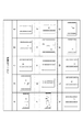
まず、コンピュータは、複数のセルのパターンのデータを取得する(S101)。コンピュータのメモリに記憶されているセルライブラリ10(不図示)の複数のセルから選択することによってデータを取得してもよいし、ユーザーによって入力された複数のセルを読み込むことでデータを取得してもよい。像性能がクリティカルなセル(解像不良を起こす可能性が高いセル)を選択してもよいし、マスク上に配置する可能性のあるすべてのセルを選択してもよい。データは、例えば、セルの設計値のGDSIIデータである。図2は、1次元レイアウト技術に用いられるホールパターンやカットパターンであって、矩形状の複数のパターン要素を含むパターンの図である。 First, the computer acquires pattern data of a plurality of cells (S101). Data may be acquired by selecting from a plurality of cells in a cell library 10 (not shown) stored in the memory of the computer, or data may be acquired by reading a plurality of cells input by a user. Also good. A cell whose image performance is critical (a cell that is highly likely to cause a resolution failure) may be selected, or all cells that are likely to be placed on the mask may be selected. The data is, for example, GDSII data of cell design values. FIG. 2 is a diagram of a hole pattern or a cut pattern used in the one-dimensional layout technique and including a plurality of rectangular pattern elements.
セルライブラリ10はセルの名称、範囲、入出力ピン情報、配線層のレイアウト物性情報を含むLEFファイル、トランジスタの寄生容量や温度電位のばらつきを含むLIBファイル、論理回路の設計データ、設計値のGDSIIデータ等のセル情報で構成される。トランジスタの拡散、ゲート、コンタクト、メタル、Via等が一つのセルに含まれている。
The
次に、S101で選択した複数のセル同士の間に光学的な近接効果が及ばない程十分離して、計算領域内に配置する(S102)。選択しているセルの数が多く、1つの計算領域に入らない場合には、複数の計算領域にセルを配置し、それぞれの計算領域を別々のコンピュータで以降の計算処理を行っても良いし、1つのコンピュータで時系列で順番に計算してもよい。つまり、選択された複数のセルを第1のセル群と第2のセル群等に分けて、各群を独立させて計算してもよい。 Next, the plurality of cells selected in S101 are sufficiently separated from each other so that the optical proximity effect does not reach them, and are arranged in the calculation region (S102). If the number of selected cells is too large to fit in one calculation area, the cells may be arranged in a plurality of calculation areas, and each calculation area may be subjected to subsequent calculation processing by a separate computer. You may calculate in order in time series with one computer. That is, a plurality of selected cells may be divided into a first cell group, a second cell group, etc., and each group may be calculated independently.
次に、複数のセルのパターンのパラメータと露光条件のパラメータの初期値を設定する(S103)。セルのパターンのパラメータは、パターンの線幅やシフト量などである。露光条件は、マスクを照明してウエハ(基板)にマスクのパターンの像を投影してウエハを露光するときの条件である。露光条件のパラメータは、露光装置の照明光学系の瞳面における光強度分布(有効光源分布)の形状や、投影光学系のNA、収差、露光波長などである。 Next, initial values of a plurality of cell pattern parameters and exposure condition parameters are set (S103). The cell pattern parameters include the line width and shift amount of the pattern. The exposure conditions are conditions for exposing the wafer by illuminating the mask and projecting an image of the mask pattern onto the wafer (substrate). The parameters of the exposure conditions are the shape of the light intensity distribution (effective light source distribution) on the pupil plane of the illumination optical system of the exposure apparatus, the NA of the projection optical system, the aberration, the exposure wavelength, and the like.
次に、設定した初期値のセルのパターンがマスクにあるとして、初期値の露光条件でマスクを照明して基板を露光した場合の、複数のセルのパターンの像を計算する(S104)。次に、計算された像を所定の評価指標(後述)を用いて評価して評価値を求める(S105)。そして、像の計算(S104)および評価値の計算(S105)が規定回数に達しているかどうかを判定する(S106)。像の計算(S104)および評価値の計算(S105)が規定回数に達していない場合には、複数のセルのパターンのパラメータ値と露光条件のパラメータ値を変更する(S107)。そして、変更されたパラメータ値を用いて像の計算(S104)および評価値の計算(S105)を行う。これらの計算を規定回数に達するまでパラメータ値を繰り返し変更して行い、複数の評価値を求める。 Next, assuming that the set initial cell pattern is in the mask, images of a plurality of cell patterns are calculated when the substrate is exposed by illuminating the mask under the initial exposure conditions (S104). Next, the calculated image is evaluated using a predetermined evaluation index (described later) to obtain an evaluation value (S105). Then, it is determined whether the image calculation (S104) and the evaluation value calculation (S105) have reached the specified number of times (S106). If the image calculation (S104) and evaluation value calculation (S105) have not reached the specified number of times, the parameter values of the patterns of the plurality of cells and the parameter values of the exposure conditions are changed (S107). Then, image calculation (S104) and evaluation value calculation (S105) are performed using the changed parameter values. These calculations are performed by repeatedly changing parameter values until the prescribed number of times is reached, and a plurality of evaluation values are obtained.
像の計算(S104)および評価値の計算(S105)が規定回数に達したら、複数の評価値のなかから、評価値が所定の評価基準を満たす場合のセルのパターンのパラメータ値を決定する(S108)。また、評価値が所定の評価基準を満たす場合の露光条件のパラメータ値を決定する(S109)。評価基準としては、最良値(最大値または最小値)としたり、予め定められた許容値としてもよい。 When the calculation of the image (S104) and the calculation of the evaluation value (S105) reach the specified number of times, the parameter value of the cell pattern when the evaluation value satisfies a predetermined evaluation criterion is determined from the plurality of evaluation values ( S108). Further, the parameter value of the exposure condition when the evaluation value satisfies a predetermined evaluation criterion is determined (S109). The evaluation standard may be the best value (maximum value or minimum value) or a predetermined allowable value.
次に、S108で決定された複数のセルのパターンのそれぞれに付加するセルの情報が作成される(S110)。そして、OPC済みのセルとして、セルライブラリ10とは別のセルライブラリ20に記憶され、マスクパターン設計に利用可能な論理素子の情報として管理される(S111)。
Next, cell information to be added to each of the plurality of cell patterns determined in S108 is created (S110). The OPC-completed cells are stored in a
なお、S106において、像の計算および評価値の計算を規定回数に達するまでパラメータ値を繰り返し変更して行った。ただし、評価値の計算(S105)の後、毎回、評価値が許容値(評価基準)を満たすかどうかを判断することにより、評価値が許容値を満たす場合にパラメータ値の決定を行ってもよい。 In S106, the calculation of the image and the calculation of the evaluation value were performed by repeatedly changing the parameter values until the specified number of times was reached. However, after the calculation of the evaluation value (S105), it is possible to determine the parameter value when the evaluation value satisfies the allowable value by determining whether the evaluation value satisfies the allowable value (evaluation standard) each time. Good.
次に、本実施形態におけるマスクのパターンの作成方法を説明する。図3は本実施形態におけるマスクのパターンの作成方法のフローチャートである。かかる作成方法は、コンピュータなどの情報処理装置によって実行される。 Next, a method for creating a mask pattern in the present embodiment will be described. FIG. 3 is a flowchart of a mask pattern generation method according to this embodiment. Such a creation method is executed by an information processing apparatus such as a computer.
S301では、ASIC等の設計仕様にもとづき論理回路設計を行い、論理素子を組み合わせた回路設計データを作成する。一般にはNetlistというフォーマットで情報が記録されていて、論理回路を組み込む箇所が記されている。S302では、S301で作成された論理素子に相当するセルをセルライブラリ20から選択する。そして、選択したセルを配置配線ツールに入力する事によりセルの配置、配線を行う(S303)。例えば、Synopsys社のIC CompilerやMentor社のOlympus−SoCなど配置配線ツールを用いてセルの配置、配線を決定する。なお、一般的なマスクパターンの作成では、OPCを施していない設計値のセルで構成されるセルライブラリ10を用いる事が多く、像性能がクリティカルでないセルに関してはセルライブラリ10から選択しても構わない。
In S301, logic circuit design is performed based on design specifications such as ASIC, and circuit design data combining logic elements is created. In general, information is recorded in a format called Netlist, and a location where a logic circuit is incorporated is described. In S302, a cell corresponding to the logic element created in S301 is selected from the
次に、マスクのレイヤー毎にパターンを抽出する(S304)。例えば、配置されたすべてのセルについて、ひとつのレイヤーパターンを抜き出してつなぎ合わせることにより、チップ全面のパターンファイルができる。一般にこれをFlatten処理と言っている。レイヤー毎に繰り返す事により、露光工程ごとにチップ全面のマスクパターン情報ができる。次に、露光条件のパラメータ値を設定する(S305)。露光条件のパラメータ値は、セルOPCの際に、S109で決定した露光条件のパラメータ値と同一の値や、近傍の値を設定する。 Next, a pattern is extracted for each layer of the mask (S304). For example, a pattern file of the entire chip surface can be created by extracting and joining one layer pattern for all the arranged cells. In general, this is called Flatten processing. By repeating each layer, mask pattern information on the entire surface of the chip can be obtained for each exposure process. Next, parameter values for exposure conditions are set (S305). As the parameter value of the exposure condition, the same value as the parameter value of the exposure condition determined in S109 or a nearby value is set during the cell OPC.
次に、レイヤー毎に抽出されたパターンのパラメータ値を設定する(S306)。次に、S306で設定したパターンがマスクに配置された場合に、S305で設定した露光条件でマスクを照明して、ウエハ上にマスクのパターンの像を投影したときの、マスクのパターンの像を計算し、像を評価する(S307)。像の評価値が所定の評価基準(許容値)を満たしているかどうかを判定する(S308)。像の評価値が評価基準を満たさない場合はS306に戻り、パターンのパラメータ値を変更して設定しなおし、像の計算および評価を行う。S306〜S308では、マスクのパターンの像が所望の結像パターン寸法に近づくように、マスクパターンの調整(OPC)が行われる。像の評価値が評価基準を満たす場合には、その場合のマスクのパターンを決定する(S309)。なお、チップ全面のOPC(S305〜S309)は、例えばMentor社のCalibreやBrion社のTachyon等でおこなっても構わない。 Next, the parameter value of the pattern extracted for each layer is set (S306). Next, when the pattern set in S306 is arranged on the mask, the mask pattern image when the mask is illuminated on the wafer under the exposure conditions set in S305 and the mask pattern image is projected onto the wafer is displayed. Calculate and evaluate the image (S307). It is determined whether the evaluation value of the image satisfies a predetermined evaluation criterion (allowable value) (S308). If the evaluation value of the image does not satisfy the evaluation criteria, the process returns to S306, the pattern parameter value is changed and set again, and the image is calculated and evaluated. In S306 to S308, the mask pattern adjustment (OPC) is performed so that the image of the mask pattern approaches the desired imaging pattern dimension. If the evaluation value of the image satisfies the evaluation criteria, the mask pattern in that case is determined (S309). Note that OPC (S305 to S309) on the entire surface of the chip may be performed by, for example, Caliber of Mentor or Tachyon of Brion.
パターンが決定されれば、マスクパターンの描画に必要なデータフォーマットの変換を行い、一般に電子ビーム描画等によりマスクが作成される(S310)。マスクのレイヤー毎にS305〜S310を繰返し処理することにより、半導体デバイスのクリティカル工程のマスクパターンの作成を行う。 If the pattern is determined, the data format necessary for drawing the mask pattern is converted, and a mask is generally created by electron beam drawing or the like (S310). By repeatedly performing S305 to S310 for each mask layer, a mask pattern for the critical process of the semiconductor device is created.
本実施形態によれば、複数のセルをまとめたセル群ごとに露光条件およびセルのパターンのパラメータを用いて光学像を計算して像性能を最良にしているため、1つのセル毎に計算をする場合よりも、より短時間で計算が可能となる。 また、本実施形態によれば、所望の像性能を有するマスクのパターンの決定を行う前に、各セルのパターンを、露光条件およびセルのパターンのパラメータを用いて像性能を最良にするように決定している。そのため、マスクのパターンの決定の前に適切な露光条件のもとに計算されたOPC済みのセルのパターンを用いることでき、マスクのパターンの決定に要する計算時間を短縮することができる。 According to the present embodiment, since the optical image is calculated by using the exposure condition and the cell pattern parameter for each cell group in which a plurality of cells are grouped, the image performance is optimized. The calculation can be performed in a shorter time than the case of doing so. In addition, according to the present embodiment, before determining a mask pattern having a desired image performance, the image performance of each cell pattern is optimized using exposure conditions and cell pattern parameters. Has been decided. Therefore, it is possible to use an OPC-completed cell pattern calculated under an appropriate exposure condition before determining the mask pattern, and to reduce the calculation time required for determining the mask pattern.
上記実施形態で説明したパターン作成方法を、20nmNodeの1D−GDRのスタンダードセルを用いたメタル工程のマスクパターンの作成に適用した実施例を説明する。 An example will be described in which the pattern creation method described in the above embodiment is applied to creation of a mask pattern in a metal process using a 20 nm Node 1D-GDR standard cell.
1D−GDRのデバイスは、微細なラインアンドスペース(L/S)パターンを形成した後L/Sのスペースの一部分を削除するカットパターンで埋め、全体をエッチングする事でアイソレーションされた溝を形成する。L/Sはセルによらず一律だが、カットパターンの数や配置は通常、セル毎に異なる。カットパターン工程のマスクを例にとって説明する。L/Sのラインの一部分を削除するGateパターン用のカットパターンでも同様である。 In 1D-GDR devices, a fine line and space (L / S) pattern is formed, then a part of the L / S space is filled with a cut pattern, and the whole is etched to form an isolated groove. To do. Although L / S is uniform regardless of the cell, the number and arrangement of cut patterns usually differ from cell to cell. An explanation will be given by taking a mask in the cut pattern process as an example. The same applies to the cut pattern for the Gate pattern in which a part of the L / S line is deleted.
露光装置の露光条件は、光源波長193.368nm、投影系開口数1.35、液浸屈折率1.437、レジスト屈折率1.683で、タンジェンシャル偏光照明を用いた。マスクはバイナリマスクで各パターン要素が黒(遮光部)で背景が白(透過部)のブライトフィールドとした。 The exposure conditions of the exposure apparatus were a light source wavelength of 193.368 nm, a projection system numerical aperture of 1.35, an immersion refractive index of 1.437, a resist refractive index of 1.683, and tangential polarization illumination. The mask was a bright field in which each pattern element was black (light-shielding portion) and the background was white (transmissive portion).
20nmNodeの1D−GDRは一般にGateピッチが84nm、Metalのピッチが64nmとなっている。したがってX方向が84nm、Y方向が64nmのL/Sをグリッドとするセルとなっている。ここでは、図4に示すような、複数のスタンダードセルの設計パターンをセルライブラリ10から選択した。 A 20 nm Node 1D-GDR generally has a Gate pitch of 84 nm and a Metal pitch of 64 nm. Therefore, the cell has a grid with L / S of 84 nm in the X direction and 64 nm in the Y direction. Here, a plurality of standard cell design patterns as shown in FIG.
各セルの領域(縦の長さ(X)、横の長さ(Y))はnm単位で以下の様になっている。
A:(1353、640)
B:( 861、640)
C:( 369、640)
D:( 369、640)
E:( 287、640)
F:(1599、640)
G:( 123、640)
H:( 205、640)
I:( 615、640)
J:( 287、640)
K:( 287、640)
L:( 369、640)
M:( 369、640)
N:( 943、640)
O:( 779、640)
The area of each cell (vertical length (X), horizontal length (Y)) is as follows in nm units.
A: (1353, 640)
B: (861, 640)
C: (369, 640)
D: (369, 640)
E: (287, 640)
F: (1599, 640)
G: (123, 640)
H: (205, 640)
I: (615, 640)
J: (287, 640)
K: (287, 640)
L: (369, 640)
M: (369, 640)
N: (943, 640)
O: (779, 640)
一般に有効光源分布を複数の要素(点光源)に分割する際の分割数が同一の場合に、光学計算の計算領域の一辺の長さは、(波長/NA)に比例する。しかし、近年、露光装置の波長とNAを変えずにセルのパターンの微細化が進んでいるため、計算領域が変わらずに、より多くのセルを計算領域内に入れられる傾向にある。上記の露光条件では、光学像の計算領域は約4.5um角となる。 In general, when the number of divisions when dividing the effective light source distribution into a plurality of elements (point light sources) is the same, the length of one side of the calculation area of the optical calculation is proportional to (wavelength / NA). However, in recent years, cell patterns have been miniaturized without changing the wavelength and NA of the exposure apparatus, so that more cells tend to be put in the calculation area without changing the calculation area. Under the above exposure conditions, the optical image calculation area is about 4.5 um square.
図5に、計算領域と複数のセルの配置の一例を示す。点線で示す枠が光学計算の計算領域で、A〜Oと記載された長方形がそれぞれのセルA〜Oを表している。各セル間のスペースをXY方向とも1um離して配置すると、選択した全15セルを3個の計算領域に配置できている。A、F、N、Oのセルを含むセル群と、B、C、D、E、I、Jのセルを含むセル群と、G、H、K、L、Mのセルを含むセル群とがそれぞれ、1つの計算領域に配置されている。したがって、パターンの光学像計算は、セルひとつずつ繰り返すと15回計算が必要なのに対し、3回ですむ。このように、複数のセルをまとめて光学像を計算することで、より短時間で計算が可能となる。 FIG. 5 shows an example of the arrangement of calculation areas and a plurality of cells. A frame indicated by a dotted line is a calculation area for optical calculation, and rectangles written as A to O represent the cells A to O, respectively. If the space between each cell is arranged 1 μm apart in the XY direction, all 15 selected cells can be arranged in three calculation areas. A cell group including A, F, N, and O cells, a cell group including B, C, D, E, I, and J cells, and a cell group including G, H, K, L, and M cells Are arranged in one calculation area. Therefore, the calculation of the optical image of the pattern requires three times, whereas the calculation of 15 times is required for each cell. In this way, by calculating an optical image by collecting a plurality of cells, the calculation can be performed in a shorter time.
各セルのパターンは、図6のパターン要素を複数含むパターンで構成されている。パターン要素(i、j)の線幅の設計値を定数Lx(i、j)、Ly(i、j)とし、パターン要素(i、j)の座標の設計値を定数Px(i、j)、Py(i、j)とする。iは図4のセルA〜Oを表す変数である。jはセル内のパターン要素の番号を示す。 Each cell pattern includes a pattern including a plurality of pattern elements shown in FIG. The design values of the line widths of the pattern elements (i, j) are constants Lx (i, j) and Ly (i, j), and the design values of the coordinates of the pattern elements (i, j) are constants Px (i, j). , Py (i, j). i is a variable representing the cells A to O in FIG. j indicates the number of the pattern element in the cell.
各パターン要素の線幅の変化量をΔlx(i、j)、Δly(i、j)として、この変数をセルのパターンのパラメータとする。また、各パターン要素の座標のシフト量をΔpx(i、j)、Δpy(i、j)として、この変数もセルのパターンのパラメータとする。なお、セルのパターンのパラメータは、パターン要素の対向する辺の距離(線幅)、例えば、Lx(i、j)+Δlx(i、j)などとしてもよい。 The amount of change in the line width of each pattern element is Δlx (i, j) and Δly (i, j), and this variable is used as a cell pattern parameter. Further, the shift amount of the coordinates of each pattern element is Δpx (i, j) and Δpy (i, j), and this variable is also used as a cell pattern parameter. The cell pattern parameter may be a distance (line width) between opposing sides of the pattern element, for example, Lx (i, j) + Δlx (i, j).
ここで、各パターン要素の線幅の設計値は、
Lx(i,j)=41nm , ∀i∀j
Ly(i,j)=64nm , ∀i∀j
とした。
Here, the design value of the line width of each pattern element is
Lx (i, j) = 41 nm, ∀i∀j
Ly (i, j) = 64 nm, ∀i∀j
It was.
複数のパターン要素が隣接する場合には、隣接する側のエッジ(境界)位置は固定という制約を用いている。 When a plurality of pattern elements are adjacent to each other, the restriction that the edge (boundary) position on the adjacent side is fixed is used.
図7に露光条件のパラメータを示す。本実施例では、露光装置の有効光源分布の形状をパラメータ化したものを露光条件のパラメータと定義している。図7の左側の図は、照明光学系の4重極照明の瞳空間を図示したもので、光強度分布(黒表示)は外σSOと内σSIとの間に挟まれ、Intxという表示のPoleの開口角Ax、Intyという表示のPoleの開口角Ayで表される。IntxとIntyの光強度は、Intxの光強度を1でノーマライズした値で表され、各Poleの光強度は均一な分布であるとしている。 FIG. 7 shows parameters of exposure conditions. In this embodiment, the parameter of the shape of the effective light source distribution of the exposure apparatus is defined as the parameter of the exposure condition. The diagram on the left side of FIG. 7 illustrates the pupil space of the quadrupole illumination of the illumination optical system, and the light intensity distribution (black display) is sandwiched between the outer σSO and the inner σSI, and Pole with a display of Intx. The aperture angle Ax and Inty are represented by the aperture angle Ay of the pole. The light intensity of Intx and Inty is represented by a value obtained by normalizing the light intensity of Intx by 1, and the light intensity of each Pole has a uniform distribution.
評価対象のパターンは、像面におけるマスクパターンの空中像を閾値Ithでスライスし、得られた等高線を結んだ図形(以下、光学像)とした。ここでは簡単のため光学像を用いたが、レジスト感光材の感光・現像特性を表すレジストパラメーターや、基板材料のエッチングパラメーター等を用いて、光学像をプロセス近接効果補正した像でもかまわない。 The pattern to be evaluated was a figure (hereinafter referred to as an optical image) obtained by slicing an aerial image of the mask pattern on the image plane with a threshold value Ith and connecting the obtained contour lines. Here, an optical image is used for the sake of simplicity, but an image obtained by correcting the optical proximity of the optical image using a resist parameter indicating the photosensitivity / development characteristics of the resist photosensitive material, an etching parameter of the substrate material, or the like may be used.
露光条件のパラメータおよびセルパターンのパラメータの可変範囲は以下のとおりとした。
0.7≦SO≦0.98
0.5≦(SO/SI)≦0.8
20°≦Ax≦90°
20°≦Ay≦90°
Intx=1
0≦Inty≦1
10≦Δlx≦100
10≦Δly≦100
−5≦Δpx≦+5
−5≦Δpy≦+5
The variable ranges of the exposure condition parameter and the cell pattern parameter were as follows.
0.7 ≦ SO ≦ 0.98
0.5 ≦ (SO / SI) ≦ 0.8
20 ° ≦ Ax ≦ 90 °
20 ° ≦ Ay ≦ 90 °
Intx = 1
0 ≦ Inty ≦ 1
10 ≦ Δlx ≦ 100
10 ≦ Δly ≦ 100
−5 ≦ Δpx ≦ + 5
−5 ≦ Δpy ≦ + 5
露光条件として、有効光源分布の形状を変数としたが、これに加えて投影光学系の開口数などを変数としても構わない。なお、閾値Ithは、0≦Ith≦1とした。 As an exposure condition, the shape of the effective light source distribution is a variable, but in addition to this, the numerical aperture of the projection optical system may be a variable. The threshold value Ith is 0 ≦ Ith ≦ 1.
パターンの像の評価対象は、各パターン要素の線幅誤差のRMSとNILSとした。また、各パターン要素の設計値中心を含むX断面の寸法CDx、および、各パターン要素の設計値中心を含むY断面の寸法CDyのEL(露光余裕度)が5%を満たす焦点深度Fも評価対象とした。また、各パターン要素の位置シフト誤差RGx、および、位置シフト誤差RGyも評価対象とした。パターン要素の線幅誤差、位置シフト誤差が最小化し、NILS、焦点深度が最大化する方が好ましいため、本実施例では、評価指標(評価関数)Pとして、下記(1)式を用いた。線幅誤差に関しては複数のセルのパターンの像の全評価点の合計のRMS値と、NILS、位置シフト誤差、焦点深度に関しては複数のセルのパターンの像の全評価点のうち最悪値(最小値)とを上記評価関数の項とした。
P=線幅誤差RMS/線幅誤差RMS許容値
+NILS許容値/(NILS最小値+0.001)
+位置シフト誤差RGx、RGyの最小値/位置シフト誤差許容値
+焦点深度許容値/(焦点深度Fの最小値+0.001) ・・・・(1)
The evaluation target of the pattern image was the RMS and NILS of the line width error of each pattern element. Also, the depth of focus F that satisfies the EL (exposure margin) of the dimension CDx of the X section including the design value center of each pattern element and the dimension CDy of the Y section including the design value center of each pattern element is evaluated. Targeted. Further, the position shift error RGx and the position shift error RGy of each pattern element were also evaluated. Since it is preferable to minimize the line width error and the position shift error of the pattern element and maximize the NILS and the focal depth, the following formula (1) is used as the evaluation index (evaluation function) P in this embodiment. Regarding the line width error, the RMS value of the total evaluation points of the image of the plurality of cell patterns and the worst value (minimum) of all evaluation points of the image of the plurality of cell patterns regarding the NILS, the position shift error, and the focal depth. Value) is defined as the term of the evaluation function.
P = Line width error RMS / Line width error RMS tolerance + NILS tolerance / (NILS minimum value + 0.001)
+ Minimum value of position shift errors RGx and RGy / allowable value of position shift error + allowable depth of focus / (minimum value of depth of focus F + 0.001) (1)
なお、線幅誤差RMS許容値=目標線幅の1%
NILS許容値=1.5
位置シフト誤差許容値=5nm
焦点深度許容値=70nm
とした。
Line width error RMS tolerance = 1% of target line width
NILS tolerance = 1.5
Position shift error tolerance = 5nm
Depth of focus tolerance = 70 nm
It was.
まず、選択したセルすべてについてパターンの像を計算し、複数のセルのパターンの像の全評価点について線幅誤差RMS、NILS、位置シフト誤差、焦点深度Fを算出する。そして、線幅誤差に関しては複数のセルのパターンの像の全評価点の合計のRMS値と、NILS、位置シフト誤差、焦点深度に関しては複数のセルのパターンの像の全評価点のうち最悪値(最小値)とを算出して、上記評価関数の値を求め、評価値とする。評価指標としては、これに限らず、複数のセルの各セルのパターンの像を評価した値を複数のセルについて合計した値や、複数のセルの各セルのパターンの像を評価した値のうち最小値または最大値などを用いて設定することができる。 First, pattern images are calculated for all selected cells, and line width errors RMS, NILS, position shift error, and depth of focus F are calculated for all evaluation points of the pattern images of a plurality of cells. With regard to the line width error, the RMS value of the total evaluation points of the image of the plurality of cell patterns, and the worst value among all the evaluation points of the image of the plurality of cell patterns regarding the NILS, the position shift error, and the focal depth. (Minimum value) is calculated, and the value of the evaluation function is obtained and set as the evaluation value. The evaluation index is not limited to this, and the value obtained by evaluating the pattern image of each cell of a plurality of cells is the sum of the values of a plurality of cells, or the value of the image of the pattern of each cell of a plurality of cells is evaluated. It can be set using a minimum value or a maximum value.
そして、上記評価指標の評価値が最小となるように各パラメータ値を変更して計算し、最適化を行った。本実施例では、露光条件のパラメータは9つ、複数のセルのパターンのパラメータが745つのトータル754つのパラメータについて最適化を行った。 Then, each parameter value was changed and calculated so as to minimize the evaluation value of the evaluation index, and optimization was performed. In the present embodiment, optimization was performed with respect to a total of 754 parameters including nine exposure condition parameters and 745 pattern parameters.
図8に最適化結果のパターンを示している。グレー(ドット)の領域部分がセルの設計値のパターン要素で、パターン要素を囲むように表示された実線の枠線が、セルOPCによる最適化後の、補正されたパターン要素の外形を表す。図8(a)が図4に示すセルA、図8(b)が図4に示すセルBの例で、セルの設計値と最適化後の形状で大きく変化している事がわかる。算出した最適化後のセルのパターンをGDSIIのデータ形式でセルライブラリ20に保存する。元の設計値のセルの情報に、このGDSIIデータを追加することにより、セルOPCのライブラリとなる。セルC〜Oも同様である。
FIG. 8 shows a pattern of optimization results. A gray (dot) area portion is a pattern element having a design value of a cell, and a solid border line displayed so as to surround the pattern element represents an outline of the corrected pattern element after optimization by the cell OPC. FIG. 8A shows an example of the cell A shown in FIG. 4 and FIG. 8B shows an example of the cell B shown in FIG. 4. It can be seen that the cell design value and the shape after optimization vary greatly. The calculated cell pattern after optimization is stored in the
有効光源分布のパラメータの最適化結果を下記に示す。
SO=0.85
Ratio=SI/SO=0.703
Ax=57°
Ay=61°
Inty=0.442
閾値Ithは、Ith=0.4086であった。
The results of optimization of the effective light source distribution parameters are shown below.
SO = 0.85
Ratio = SI / SO = 0.703
Ax = 57 °
Ay = 61 °
Inty = 0.442
The threshold value Ith was Ith = 0.4086.
本実施例では評価指標を1つとしたが、これに限らない。例えば、互いに異なる複数の評価指標を設定すれば、セルのパターンや露光条件の最適化結果が変わる。つまり、それぞれの評価指標について決定されたセルのパターンのパラメータ値は互いに異なる。このように各評価指標の設定を用いて決定されたセルのパターンを、各セルライブラリを作成して保存し、用途に合わせて適したセルライブラリを選択しても良い。また、最適化後の露光条件のパラメータとセルのパターンのパラメータの組合せを複数組、記憶媒体に保存し、管理してもよい。 In this embodiment, there is one evaluation index, but the present invention is not limited to this. For example, if a plurality of different evaluation indexes are set, the optimization result of the cell pattern and exposure conditions changes. That is, the parameter values of the cell pattern determined for each evaluation index are different from each other. In this way, the cell pattern determined using the setting of each evaluation index may be created by storing each cell library, and a cell library suitable for the application may be selected. Further, a plurality of combinations of optimized exposure condition parameters and cell pattern parameters may be stored and managed in a storage medium.
次に、保存されたOPC済みのセルライブラリに含まれる各セルを用いて、マスクパターンを作成する方法を説明する。図9は、セルライブラリからOPC済みのセルを選択して、セルのパターンを隣接配置した後のパターンを示す。簡単のため、セルA〜Oに含まれる任意のスタンダードセルを5×5に隣接配置し、合計25個分のセルでテストチップを形成した。上下の隣接セルはMetalの1グリッドピッチ分だけ離れて接合している。 Next, a method for creating a mask pattern using each cell included in the stored OPC-completed cell library will be described. FIG. 9 shows a pattern after selecting an OPC-completed cell from the cell library and arranging the cell patterns adjacent to each other. For simplicity, arbitrary standard cells included in cells A to O are arranged adjacent to 5 × 5, and a test chip is formed with a total of 25 cells. The upper and lower adjacent cells are joined apart by one grid pitch of Metal.
露光条件として、光源波長193.368nm、投影系開口数1.35、液浸屈折率1.437、レジスト屈折率1.683、タンジェンシャル偏光照明を用いた。ここでは、有効光源分布のパラメータとして、上記の最適化された結果の値と同一の値を用いたが、同一でなくても構わない。例えば、外σSO2、外σと内σの比Ratio2、X方向のPoleの開口角Ax2,Y方向のPoleの開口角Ay2,X方向のPoleの光強度Intx2,Y方向のPoleの光強度Inty2が、下記の範囲などでも可能である。
e=0.2
e2=60
e3=0.5
SO*(1−e)≦SO2≦SO*(1+e)
Ratio*(1−e)≦Ratio2≦Ratio*(1+e)
Ax−e2≦Ax2≦Ax+e2
Ay−e2≦Ay2≦Ay+e2
Intx*(1−e3)≦Intx2≦Intx*(1+e3)
Inty*(1−e3)≦Inty2≦Inty*(1+e3)
As exposure conditions, a light source wavelength of 193.368 nm, a projection system numerical aperture of 1.35, an immersion refractive index of 1.437, a resist refractive index of 1.683, and tangential polarization illumination were used. Here, although the same value as the value of the optimized result is used as the effective light source distribution parameter, it may not be the same. For example, the
e = 0.2
e2 = 60
e3 = 0.5
SO * (1-e) ≦ SO2 ≦ SO * (1 + e)
Ratio * (1-e) ≦ Ratio2 ≦ Ratio * (1 + e)
Ax−e2 ≦ Ax2 ≦ Ax + e2
Ay−e2 ≦ Ay2 ≦ Ay + e2
Intx * (1-e3) ≦ Intx2 ≦ Intx * (1 + e3)
Inty * (1-e3) ≦ Inty2 ≦ Inty * (1 + e3)
例えば、外σについては、上記の最適化された結果の値SOよりも、所定量eだけ異なる範囲で変更することできる。 For example, the outer σ can be changed within a range that differs from the optimized result value SO by a predetermined amount e.
マスクはバイナリマスクでパターン部が黒で背景白のブライトフィールドとした。 The mask was a bright mask with a binary mask, black pattern, and white background.
そして、露光条件のパラメータ値を設定して、図9に示すパターンを初期値として設定し、各パターンの像を計算しながら、各パターンにOPCを施し、各パターンのパラメータを変化させながら最適化を行った。 Then, the parameter values of the exposure conditions are set, the patterns shown in FIG. 9 are set as initial values, the images of each pattern are calculated, OPC is applied to each pattern, and the parameters of each pattern are changed and optimized Went.
各パターン要素の設計値中心を含むX断面の寸法をCDx、Y断面の寸法をCDy、として、全パターン要素の設計値からの差のRMSを評価指標に用いた。RMSの式を以下に示す。 The dimension of the X cross section including the design value center of each pattern element is CDx, the dimension of the Y cross section is CDy, and the RMS of the difference from the design value of all the pattern elements is used as an evaluation index. The formula of RMS is shown below.

なお、nxはX断面の総評価数、nyはY断面の総評価数とし、CDx0(i,j)、CDy0(i,j)は設計値とする。 Note that nx is the total evaluation number of the X section, ny is the total evaluation number of the Y section, and CDx0 (i, j) and CDy0 (i, j) are design values.
図10に結果を示す。図10に示すグレー(ドット)の領域部分が、設計値セルのパターンを表し、グレーのパターンを囲むように表示された実線の枠線がチップ全体で補正されたパターンの外形を表す。 The results are shown in FIG. The gray (dot) area portion shown in FIG. 10 represents the design value cell pattern, and the solid line border line displayed so as to surround the gray pattern represents the outline of the pattern corrected for the entire chip.
また、図11に、OPCのための光学計算の計算回数とマスクパターンのCDのRMS(CDRMS)をプロットした。図11は横軸にOPCのための光学計算の計算回数、縦軸に残さCDRMSをプロットしている。Iは、本実施例のように、OPC済みのセルをセルライブラリから選択してチップに配置して、チップ全体にOPCを施した場合の結果である。IIは、OPCを施していない設計値のセルをセルライブラリから選択してチップに配置して、チップ全体にOPCを施した場合の比較例1の結果である。 FIG. 11 plots the number of optical calculations for OPC and the RMS (CDRMS) of the mask pattern CD. FIG. 11 plots the number of optical calculations for OPC on the horizontal axis and the remaining CDRMS on the vertical axis. I is the result when the OPC-completed cell is selected from the cell library and arranged on the chip, and the entire chip is subjected to OPC as in this embodiment. II shows the result of Comparative Example 1 in which a cell having a design value not subjected to OPC is selected from the cell library and arranged on the chip, and OPC is applied to the entire chip.
CDRMSの許容値を2%とすると、Iの場合には計算回数5回、IIの場合には計算回数10回で許容値に達することがわかる。つまり、Iの場合には、IIの場合と比較して、計算回数が約1/2となる。よって、チップレベルのOPCに要する計算時間は約1/2となっている。一方、規定の計算回数を7回にした場合には、Iの場合には1.02%、IIの場合にはCDRMSは7.49%となっている。つまり、Iの場合の方が、一定の計算回数(時間内)で到達するCDRMS残さの値が小さい。したがって、本実施例のマスクパターンの作成方法によれば、所望の解像性能を有するマスクのパターンをより短い時間で作成することができる。Iのマスクパターンで像性能を評価し、EL5%時のDOF69nmを得た。
Assuming that the allowable value of CDRMS is 2%, the allowable value is reached when the number of calculations is 5 in the case of I and 10 times in the case of II. That is, in the case of I, the number of calculations is about ½ compared to the case of II. Therefore, the calculation time required for chip-level OPC is about ½. On the other hand, when the prescribed number of calculations is 7, the CDRS is 7.49% for I and 1.02% for II. That is, in the case of I, the value of the CDRMS residual that is reached after a certain number of calculations (within time) is smaller. Therefore, according to the mask pattern creation method of this embodiment, a mask pattern having a desired resolution performance can be created in a shorter time. The image performance was evaluated with a mask pattern of I, and a DOF of 69 nm at
像性能の到達度を評価するため、チップ配置後のマスクパターンを用いて(1)の評価指標を用いて露光条件とマスクパターンの最適化を行った。約3000回の計算でCDRMSが2%に収束し、かつEL5%時のDOF68nmを得た。600倍の計算回数を要するこの結果で得られた像性能は、Iのマスクでの結果と同等である。つまり、本実施例のマスクパターン作成方法によれば、少ない計算回数で、CDRMSのみならずDOFも良好な性能を得る事ができることがわかる。
In order to evaluate the reach of image performance, the exposure conditions and the mask pattern were optimized using the evaluation index of (1) using the mask pattern after chip placement. The CDRMS converged to 2% in about 3000 calculations, and a DOF of 68 nm at
さらに、従来例との比較のため、比較例2として、セルのパターンを決定する際に、露光条件のパラメータ値を変更せずに、複数のセルのパターンのパラメータ値のみを変更して、セルOPCの計算を行った。各セルのパターンのパラメータは以下の5つで、パラメータ値の可変範囲は以下のとおりである。
10≦ΔLx≦100
10≦ΔLx≦100
−5≦Δpx≦+5
−5≦Δpy≦+5
なお、SO=0.98(固定値)、Ratio=SI/SO=0.7(固定値)であって、0≦Ith≦1とした。4分割ではなく、輪帯形状の有効光源を用いた。
Further, for comparison with the conventional example, as a comparative example 2, when determining the cell pattern, only the parameter values of the plurality of cell patterns are changed without changing the parameter values of the exposure conditions. OPC was calculated. The parameters of each cell pattern are the following five, and the variable range of the parameter value is as follows.
10 ≦ ΔLx ≦ 100
10 ≦ ΔLx ≦ 100
−5 ≦ Δpx ≦ + 5
−5 ≦ Δpy ≦ + 5
Note that SO = 0.98 (fixed value), Ratio = SI / SO = 0.7 (fixed value), and 0 ≦ Ith ≦ 1. An effective light source having an annular shape was used instead of four divisions.
パターンの像の評価対象、および、評価指標は本実施例と同じとした。なお、繰返し計算の回数は200回以内とした。そして、セルのパターンの補正を行った後、決定されたセルのパターンのデータを、メモリのセルライブラリ30に記憶保存した。そして、セルライブラリ30からセルを選択して、図9に示すようにスタンダードセル25個を隣接配置したテストチップパターンを作製した。
The evaluation target of the pattern image and the evaluation index were the same as in this example. The number of repeated calculations was set to 200 times or less. Then, after correcting the cell pattern, the determined cell pattern data was stored in the
そして、本実施例のマスクパターンの作成方法と同様に計算を行った。図12に示すように、OPCのための光学計算の計算回数とマスクパターンのCDのRMSをプロットした。Iは本実施例の結果であり、IIIは比較例2の結果である。CDRMSの許容値を2%とすると、Iの場合には計算回数5回、IIIの場合には計算回数7回で許容値に達することがわかる。つまり、Iの場合にはIIIの場合と比較して、計算回数が減り、計算時間が短くなっている。一方、規定の計算回数を7回にした場合には、Iの場合には1.02%、IIIの場合にはCDRMSは1.87%となっている。つまり、Iの場合の方が、一定の計算回数(時間内)で到達するCDRMS残さの値が小さい。したがって、本実施例のマスクパターンの作成方法によれば、所望の解像性能を有するマスクのパターンをより短い時間で作成することができる。IIIの場合では、セルのパターンの決定の際に適切な露光条件が設定されておらず、その露光条件でOPCを施したセルを配置し、マスクパターンの初期値としたため、露光条件の変更によるマスクパターンの補正量が大きいため計算時間が長くかかっている。 The calculation was performed in the same manner as in the mask pattern creation method of the present example. As shown in FIG. 12, the number of optical calculations for OPC and the RMS of the mask pattern CD were plotted. I is the result of this example, and III is the result of Comparative Example 2. Assuming that the allowable value of CDRMS is 2%, the allowable value is reached after 5 calculations for I and 7 calculations for III. That is, in the case of I, the number of calculations is reduced and the calculation time is shorter than in the case of III. On the other hand, when the prescribed number of calculations is 7, the CDRMS is 1.87% for I and 1.87% for III. That is, in the case of I, the value of the CDRMS residual that is reached after a certain number of calculations (within time) is smaller. Therefore, according to the mask pattern creation method of this embodiment, a mask pattern having a desired resolution performance can be created in a shorter time. In the case of III, an appropriate exposure condition is not set at the time of determining a cell pattern, and a cell subjected to OPC under the exposure condition is arranged and used as an initial value of the mask pattern. Since the mask pattern correction amount is large, the calculation time is long.
本実施例によれば、マスクのパターンの決定を行う前に、各セルのパターンを、露光条件およびセルのパターンのパラメータを用いて像性能を最良にするように決定する。これにより、マスクのパターンの決定に要する計算時間を短縮することができ、像性能の良い解が得られる。 According to the present embodiment, before determining the mask pattern, the pattern of each cell is determined so as to optimize the image performance using the exposure conditions and the parameters of the cell pattern. As a result, the calculation time required for determining the mask pattern can be shortened, and a solution with good image performance can be obtained.
1次元レイアウトに用いられるパターンは、等グリッド上に配置された矩形状のパターンなど単純なパターンであるため、L字状のパターンなど縦と横方向に延びるパターンに比べ、露光条件の変化によって、OPCを施す際のパターンの補正量は大きく変化しない。縦と横方向に延び、等グリッド上にのらずに配置されたセルパターンでは、セル同士を隣接配置した際に、パターンの境界部や角部での補正量が大きくなってしまったり、複雑なパターンの補正が必要になってしまう事がある。これらはどちらもOPCの計算時間を増大させてしまう。したがって、本実施形態、実施例におけるセルのパターンの作成方法およびマスクパターン作成方法は、1次元レイアウトに用いられるパターンに好適である。 The pattern used for the one-dimensional layout is a simple pattern such as a rectangular pattern arranged on an equal grid. Therefore, compared to a pattern extending in the vertical and horizontal directions, such as an L-shaped pattern, the exposure conditions change, The pattern correction amount when performing OPC does not change significantly. In cell patterns that extend vertically and horizontally and do not lie on an equal grid, when cells are placed adjacent to each other, the amount of correction at the borders and corners of the pattern becomes large and complicated. Correct pattern correction may be required. Both of these increase the OPC calculation time. Therefore, the cell pattern creation method and the mask pattern creation method in the present embodiment and examples are suitable for patterns used in one-dimensional layouts.
さらに、本実施例のセルのパターンの作成方法により作成されたセルは、様々なデバイスのレイアウト設計に適用可能であるため、様々なデバイスのパターンの作成時間の短縮にもなる。 Furthermore, since the cells created by the cell pattern creation method of this embodiment can be applied to various device layout designs, the creation time of various device patterns can be shortened.
本発明は、以下の処理を実行することによっても実現される。即ち、上述の実施形態、実施例の機能を実現するソフトウェア(プログラム)を、ネットワーク又は各種記憶媒体を介してシステム或いは装置に供給し、そのシステム或いは装置のコンピュータ(又はCPUやMPU等)がプログラムを読み出して実行する処理である。 The present invention is also realized by executing the following processing. That is, software (program) that realizes the functions of the above-described embodiments and examples is supplied to a system or apparatus via a network or various storage media, and a computer (or CPU, MPU, or the like) of the system or apparatus is programmed. Is read and executed.
次に、デバイス(液晶表示デバイス等)の製造方法について説明する。液晶表示デバイスは、透明電極を形成する工程を経ることにより製造される。透明電極を形成する工程は、透明導電膜が蒸着されたガラス基板に感光剤を塗布する工程と、マスクを露光装置に搭載して、感光剤が塗布されたガラス基板を露光する工程と、ガラス基板を現像する工程を含む。マスクは、上記のように作成されたマスクのパターンを用いて製造される。 Next, a method for manufacturing a device (liquid crystal display device or the like) will be described. A liquid crystal display device is manufactured through a process of forming a transparent electrode. The step of forming a transparent electrode includes a step of applying a photosensitive agent to a glass substrate on which a transparent conductive film is deposited, a step of mounting a mask on an exposure device, and exposing a glass substrate on which the photosensitive agent is applied, and a glass Developing the substrate. The mask is manufactured using the mask pattern created as described above.
上述の露光装置を利用したデバイス製造方法は、液晶表示デバイスの他に、例えば、半導体デバイス等のデバイスの製造にも好適である。前記方法は、上記のように製造されたマスクを露光装置に搭載して、感光剤が塗布された基板を露光する工程と、前記露光された基板を現像する工程とを含みうる。さらに、前記デバイス製造方法は、他の周知の工程(酸化、成膜、蒸着、ドーピング、平坦化、エッチング、レジスト剥離、ダイシング、ボンディング、パッケージング等)を含みうる。 The device manufacturing method using the above-described exposure apparatus is suitable for manufacturing a device such as a semiconductor device in addition to the liquid crystal display device. The method may include a step of mounting the mask manufactured as described above on an exposure apparatus, exposing a substrate coated with a photosensitive agent, and developing the exposed substrate. Furthermore, the device manufacturing method may include other well-known steps (oxidation, film formation, vapor deposition, doping, planarization, etching, resist stripping, dicing, bonding, packaging, and the like).
以上、本発明の好ましい実施形態について説明したが、本発明はこれらの実施形態に限定されないことはいうまでもなく、その要旨の範囲内で種々の変形及び変更が可能である。 As mentioned above, although preferable embodiment of this invention was described, it cannot be overemphasized that this invention is not limited to these embodiment, A various deformation | transformation and change are possible within the range of the summary.
Claims (11)
複数種類の前記セルのパターンのデータを取得する取得工程と、
前記セルのパターンが照明され基板に前記セルのパターンの像が投影されて前記基板が露光されるときの露光条件のパラメータ値と、前記セルのパターンのパラメータ値と、を設定する設定工程と、
設定された前記露光条件のパラメータ値と前記セルのパターンのパラメータ値とを用いて、光学計算用の1つの計算領域において、該取得した前記複数種類のセル同士が光学的な近接効果を及ぼさない距離に離して前記複数種類のセルを並べて配置して、当該設定された露光条件における前記複数種類のセルのパターンの光学像を前記計算領域で計算して、計算された前記複数種類のセルのパターンの光学像の評価値を求める計算工程と、
設定した前記露光条件のパラメータ値と、前記セルのパターンのパラメータ値と、を変更する変更工程と、
変更後のパラメータ値を用いて前記光学像を計算して、計算された前記光学像の前記評価値を求める前記計算工程と、前記変更工程と、を繰り返す工程と、
前記繰り返し工程において求められた前記評価値のうち所定の評価基準を満たす場合の前記セルのパターンのパラメータ値をもつパターンを、前記マスクのパターンを作成するための複数種類のセルのパターンとして決定する決定工程と、
決定された前記複数種類のセルのパターンをセルのライブラリに記憶する記憶工程と、を有することを特徴とするパターン作成方法。 A pattern creation method for creating a cell pattern of a cell library used for creating a mask pattern using a computer,
An acquisition step of acquiring pattern data of a plurality of types of cells;
A setting step of setting a parameter value of an exposure condition when the cell pattern is illuminated and an image of the cell pattern is projected onto the substrate to expose the substrate, and a parameter value of the cell pattern;
Using the set parameter value of the exposure condition and the parameter value of the cell pattern, the obtained plural types of cells do not exert an optical proximity effect in one calculation area for optical calculation. distance apart and arranged side by side said plurality of types of cells, the optical image of the pattern of the set Keru Contact exposure conditions the plurality of types of cells calculated in the calculation area, calculated in the plurality of types A calculation step for obtaining an evaluation value of an optical image of a cell pattern;
A changing step for changing the set parameter value of the exposure condition and the parameter value of the cell pattern;
Calculating the optical image using the parameter value after the change, obtaining the evaluation value of the calculated optical image, and repeating the changing step;
A pattern having a parameter value of the cell pattern when satisfying a predetermined evaluation criterion among the evaluation values obtained in the repetition step is determined as a plurality of types of cell patterns for creating the mask pattern. A decision process;
Pattern forming method characterized by having a storage step, a storing pattern of the determined plurality of types of cells in the library of the cell.
前記決定工程において、前記複数の評価指標について、前記評価値が所定の評価基準を満たす場合の前記セルのパターンのパラメータ値を決定することを特徴とする請求項1乃至4の何れか1項に記載のパターン作成方法。 In the calculation step, an evaluation value of the optical image is obtained using a plurality of evaluation indexes,
The parameter value of the pattern of the cell when the evaluation value satisfies a predetermined evaluation criterion is determined for the plurality of evaluation indexes in the determination step. The pattern creation method described.
光学計算用の1つの計算領域において、該取得した前記複数種類のセルのうち一部の前記複数種類のセル同士が光学的な近接効果を及ぼさない距離に離して前記一部の複数種類のセルを並べて配置して、当該設定された露光条件における前記一部の複数種類のセルのパターンの光学像を前記1つの計算領域で計算し、In one calculation area for optical calculation, the plurality of the plurality of types of cells obtained by separating the plurality of the plurality of types of cells from each other at a distance that does not exert an optical proximity effect. Are arranged side by side to calculate an optical image of the pattern of the plurality of types of some of the cells under the set exposure conditions in the one calculation area,
光学計算用の他の1つの計算領域において、該取得した前記複数種類のセルのうち他の一部の前記複数種類のセル同士が光学的な近接効果を及ぼさない距離に離して前記他の一部の複数種類のセルを並べて配置して、当該設定された露光条件における前記他の一部の複数種類のセルのパターンの光学像を前記他の1つの計算領域で計算する、ことを特徴とする請求項1乃至7の何れか1項に記載のパターン作成方法。In another calculation area for optical calculation, the other one of the plurality of types of acquired cells is separated by a distance that does not exert an optical proximity effect. A plurality of types of cells arranged side by side, and an optical image of the pattern of the other part of the plurality of types of cells under the set exposure conditions is calculated in the other one calculation region, The pattern creation method according to any one of claims 1 to 7.
Priority Applications (5)
| Application Number | Priority Date | Filing Date | Title |
|---|---|---|---|
| JP2012131117A JP6108693B2 (en) | 2012-06-08 | 2012-06-08 | Pattern creation method |
| US13/908,773 US9672300B2 (en) | 2012-06-08 | 2013-06-03 | Pattern generation method |
| TW102118942A TWI485509B (en) | 2012-06-08 | 2013-06-05 | Pattern generation method |
| KR1020130065142A KR20130138131A (en) | 2012-06-08 | 2013-06-07 | Pattern generation method |
| CN201310226984.0A CN103488043A (en) | 2012-06-08 | 2013-06-08 | Pattern generation method |
Applications Claiming Priority (1)
| Application Number | Priority Date | Filing Date | Title |
|---|---|---|---|
| JP2012131117A JP6108693B2 (en) | 2012-06-08 | 2012-06-08 | Pattern creation method |
Publications (3)
| Publication Number | Publication Date |
|---|---|
| JP2013254165A JP2013254165A (en) | 2013-12-19 |
| JP2013254165A5 JP2013254165A5 (en) | 2015-07-23 |
| JP6108693B2 true JP6108693B2 (en) | 2017-04-05 |
Family
ID=49715062
Family Applications (1)
| Application Number | Title | Priority Date | Filing Date |
|---|---|---|---|
| JP2012131117A Active JP6108693B2 (en) | 2012-06-08 | 2012-06-08 | Pattern creation method |
Country Status (5)
| Country | Link |
|---|---|
| US (1) | US9672300B2 (en) |
| JP (1) | JP6108693B2 (en) |
| KR (1) | KR20130138131A (en) |
| CN (1) | CN103488043A (en) |
| TW (1) | TWI485509B (en) |
Families Citing this family (10)
| Publication number | Priority date | Publication date | Assignee | Title |
|---|---|---|---|---|
| JP2014072226A (en) * | 2012-09-27 | 2014-04-21 | Tokyo Electron Ltd | Pattern formation method |
| TWI528201B (en) * | 2013-08-28 | 2016-04-01 | 旺宏電子股份有限公司 | Advanced correction method |
| JP6338368B2 (en) * | 2013-12-25 | 2018-06-06 | キヤノン株式会社 | Method for evaluating pattern optical image |
| JP6399751B2 (en) * | 2013-12-25 | 2018-10-03 | キヤノン株式会社 | Mask pattern creation method, program, mask manufacturing method, exposure method, and article manufacturing method |
| TWI620005B (en) * | 2014-08-18 | 2018-04-01 | 聯華電子股份有限公司 | Layout pattern decomposition method |
| US10380307B1 (en) * | 2016-03-30 | 2019-08-13 | Silicon Technologies, Inc. | Analog design tool, cell set, and related methods, systems and equipment |
| US10283526B2 (en) * | 2016-12-21 | 2019-05-07 | Qualcomm Incorporated | Standard cell circuits employing voltage rails electrically coupled to metal shunts for reducing or avoiding increases in voltage drop |
| KR20220000929A (en) * | 2017-03-31 | 2022-01-04 | 가부시키가이샤 니콘 | Pattern calculation apparatus, pattern calculation method, mask, exposure apparatus, device production method, computer program, and recording medium |
| WO2020154979A1 (en) * | 2019-01-30 | 2020-08-06 | 深圳晶源信息技术有限公司 | Photolithography mask optimization method and apparatus for pattern and image joint optimization, and electronic device |
| CN113572973B (en) * | 2021-09-28 | 2021-12-17 | 武汉市聚芯微电子有限责任公司 | Exposure control method, device, equipment and computer storage medium |
Family Cites Families (23)
| Publication number | Priority date | Publication date | Assignee | Title |
|---|---|---|---|---|
| US5682323A (en) * | 1995-03-06 | 1997-10-28 | Lsi Logic Corporation | System and method for performing optical proximity correction on macrocell libraries |
| JP3827659B2 (en) * | 1999-03-04 | 2006-09-27 | 松下電器産業株式会社 | LSI mask data creation method and LSI pattern formation method |
| JP2004079714A (en) | 2002-08-14 | 2004-03-11 | Renesas Technology Corp | Optimal configuration determining device for aperture |
| EP1450206B1 (en) | 2003-02-21 | 2016-04-20 | Canon Kabushiki Kaisha | Mask and its manufacturing method, exposure, and semiconductor device fabrication method |
| US7349066B2 (en) | 2005-05-05 | 2008-03-25 | Asml Masktools B.V. | Apparatus, method and computer program product for performing a model based optical proximity correction factoring neighbor influence |
| JP4336671B2 (en) * | 2005-07-15 | 2009-09-30 | キヤノン株式会社 | A program for causing a computer to determine exposure parameters, a determination method for determining exposure parameters, an exposure method, and a device manufacturing method. |
| KR101330344B1 (en) | 2005-09-13 | 2013-11-15 | 루미네슨트 테크놀로지, 인크. | Systems, masks, and methods for photolithography |
| US7650587B2 (en) | 2006-11-30 | 2010-01-19 | International Business Machines Corporation | Local coloring for hierarchical OPC |
| CN100445875C (en) | 2007-01-26 | 2008-12-24 | 浙江大学 | Method for correcting layering optical proximity effect |
| JP5077656B2 (en) | 2007-06-18 | 2012-11-21 | 株式会社ニコン | Pattern data processing method and system, and exposure method and apparatus |
| US7927782B2 (en) * | 2007-12-28 | 2011-04-19 | Texas Instruments Incorporated | Simplified double mask patterning system |
| TWI364064B (en) | 2008-01-24 | 2012-05-11 | United Microelectronics Corp | Method of checking and correcting mask pattern |
| JP2009182237A (en) * | 2008-01-31 | 2009-08-13 | Toshiba Corp | Exposure condition setting method, pattern designing method and manufacturing method of semiconductor device |
| JP5153492B2 (en) * | 2008-07-11 | 2013-02-27 | キヤノン株式会社 | Exposure condition determining method and computer program |
| JP5142952B2 (en) | 2008-11-11 | 2013-02-13 | ルネサスエレクトロニクス株式会社 | Photomask pattern correction method and manufacturing method, semiconductor device manufacturing method, pattern correction device, and program |
| JP5239970B2 (en) * | 2009-03-17 | 2013-07-17 | 富士通株式会社 | Leak current calculation program, leak current calculation device, and leak current calculation method |
| KR101667655B1 (en) | 2009-10-26 | 2016-10-20 | 삼성전자주식회사 | Methods of compensating patterns for a semiconductor device |
| US8739079B2 (en) * | 2009-10-30 | 2014-05-27 | Canon Kabushiki Kaisha | Recording medium and determination method |
| US8745554B2 (en) * | 2009-12-28 | 2014-06-03 | Taiwan Semiconductor Manufacturing Company, Ltd. | Practical approach to layout migration |
| JP5627394B2 (en) * | 2010-10-29 | 2014-11-19 | キヤノン株式会社 | Program for determining mask data and exposure conditions, determination method, mask manufacturing method, exposure method, and device manufacturing method |
| JP2012099596A (en) | 2010-11-01 | 2012-05-24 | Panasonic Corp | Optimization method of lighting shape, optimization method of mask shape, and pattern formation method |
| NL2007642A (en) * | 2010-11-10 | 2012-05-14 | Asml Netherlands Bv | Optimization flows of source, mask and projection optics. |
| CN102147567B (en) | 2011-04-01 | 2012-10-03 | 中国科学院微电子研究所 | Cell-based hierarchical optical proximity correction (OPC) method |
-
2012
- 2012-06-08 JP JP2012131117A patent/JP6108693B2/en active Active
-
2013
- 2013-06-03 US US13/908,773 patent/US9672300B2/en active Active
- 2013-06-05 TW TW102118942A patent/TWI485509B/en active
- 2013-06-07 KR KR1020130065142A patent/KR20130138131A/en not_active Application Discontinuation
- 2013-06-08 CN CN201310226984.0A patent/CN103488043A/en active Pending
Also Published As
| Publication number | Publication date |
|---|---|
| TW201351032A (en) | 2013-12-16 |
| JP2013254165A (en) | 2013-12-19 |
| US9672300B2 (en) | 2017-06-06 |
| KR20130138131A (en) | 2013-12-18 |
| TWI485509B (en) | 2015-05-21 |
| US20130329202A1 (en) | 2013-12-12 |
| CN103488043A (en) | 2014-01-01 |
Similar Documents
| Publication | Publication Date | Title |
|---|---|---|
| JP6108693B2 (en) | Pattern creation method | |
| JP4538021B2 (en) | Optical proximity correction method | |
| US11079672B2 (en) | Method and system for layout enhancement based on inter-cell correlation | |
| US6567972B1 (en) | Method and apparatus for correcting mask pattern, mask having corrected mask pattern, and storage medium storing program for executing the method for correcting mask pattern | |
| JP4709511B2 (en) | Mask pattern correction method, mask pattern correction program, photomask manufacturing method, and semiconductor device manufacturing method | |
| CN109559979A (en) | Manufacturing method for integrated curcuit | |
| JP2014240899A (en) | Preparation method of mask pattern, program, and information processing device | |
| KR20170048281A (en) | Pattern generation method, program, information processing apparatus, and mask fabrication method | |
| US9547230B2 (en) | Method for evaluating optical image of pattern, recording medium, and information processing apparatus | |
| JP5575024B2 (en) | Mask pattern correction method, mask pattern correction program, and semiconductor device manufacturing method | |
| JP5665915B2 (en) | How to create mask data | |
| JP2004157160A (en) | Method for forming process model, method for designing mask pattern, mask and method for manufacturing semiconductor device | |
| KR101911993B1 (en) | Method for generating pattern, storage medium, and information processing apparatus | |
| JP5980065B2 (en) | Mask data creation method, program, information processing apparatus, mask manufacturing method, exposure method, and device manufacturing method | |
| US20230168576A1 (en) | Full-chip cell critical dimension correction method and method of manufacturing mask using the same | |
| KR20230082519A (en) | Method for optical proximity correction and method of manufacturing semiconductor device having the same | |
| CN113219785A (en) | Method for verifying optical proximity correction |
Legal Events
| Date | Code | Title | Description |
|---|---|---|---|
| A521 | Request for written amendment filed |
Free format text: JAPANESE INTERMEDIATE CODE: A523 Effective date: 20150608 |
|
| A621 | Written request for application examination |
Free format text: JAPANESE INTERMEDIATE CODE: A621 Effective date: 20150608 |
|
| A977 | Report on retrieval |
Free format text: JAPANESE INTERMEDIATE CODE: A971007 Effective date: 20160324 |
|
| A131 | Notification of reasons for refusal |
Free format text: JAPANESE INTERMEDIATE CODE: A131 Effective date: 20160329 |
|
| A521 | Request for written amendment filed |
Free format text: JAPANESE INTERMEDIATE CODE: A523 Effective date: 20160527 |
|
| A131 | Notification of reasons for refusal |
Free format text: JAPANESE INTERMEDIATE CODE: A131 Effective date: 20160920 |
|
| A521 | Request for written amendment filed |
Free format text: JAPANESE INTERMEDIATE CODE: A523 Effective date: 20161121 |
|
| TRDD | Decision of grant or rejection written | ||
| A01 | Written decision to grant a patent or to grant a registration (utility model) |
Free format text: JAPANESE INTERMEDIATE CODE: A01 Effective date: 20170207 |
|
| A61 | First payment of annual fees (during grant procedure) |
Free format text: JAPANESE INTERMEDIATE CODE: A61 Effective date: 20170307 |
|
| R151 | Written notification of patent or utility model registration |
Ref document number: 6108693 Country of ref document: JP Free format text: JAPANESE INTERMEDIATE CODE: R151 |