JP6103825B2 - Semiconductor integrated circuit, information processing device - Google Patents
Semiconductor integrated circuit, information processing device Download PDFInfo
- Publication number
- JP6103825B2 JP6103825B2 JP2012129885A JP2012129885A JP6103825B2 JP 6103825 B2 JP6103825 B2 JP 6103825B2 JP 2012129885 A JP2012129885 A JP 2012129885A JP 2012129885 A JP2012129885 A JP 2012129885A JP 6103825 B2 JP6103825 B2 JP 6103825B2
- Authority
- JP
- Japan
- Prior art keywords
- power control
- power
- control target
- target unit
- clock
- Prior art date
- Legal status (The legal status is an assumption and is not a legal conclusion. Google has not performed a legal analysis and makes no representation as to the accuracy of the status listed.)
- Active
Links
Images


Classifications
-
- G—PHYSICS
- G06—COMPUTING; CALCULATING OR COUNTING
- G06F—ELECTRIC DIGITAL DATA PROCESSING
- G06F1/00—Details not covered by groups G06F3/00 - G06F13/00 and G06F21/00
- G06F1/26—Power supply means, e.g. regulation thereof
- G06F1/32—Means for saving power
- G06F1/3203—Power management, i.e. event-based initiation of a power-saving mode
- G06F1/3234—Power saving characterised by the action undertaken
- G06F1/324—Power saving characterised by the action undertaken by lowering clock frequency
-
- G—PHYSICS
- G06—COMPUTING; CALCULATING OR COUNTING
- G06F—ELECTRIC DIGITAL DATA PROCESSING
- G06F1/00—Details not covered by groups G06F3/00 - G06F13/00 and G06F21/00
- G06F1/24—Resetting means
-
- G—PHYSICS
- G06—COMPUTING; CALCULATING OR COUNTING
- G06F—ELECTRIC DIGITAL DATA PROCESSING
- G06F1/00—Details not covered by groups G06F3/00 - G06F13/00 and G06F21/00
- G06F1/26—Power supply means, e.g. regulation thereof
- G06F1/32—Means for saving power
- G06F1/3203—Power management, i.e. event-based initiation of a power-saving mode
- G06F1/3234—Power saving characterised by the action undertaken
- G06F1/3237—Power saving characterised by the action undertaken by disabling clock generation or distribution
-
- G—PHYSICS
- G06—COMPUTING; CALCULATING OR COUNTING
- G06F—ELECTRIC DIGITAL DATA PROCESSING
- G06F1/00—Details not covered by groups G06F3/00 - G06F13/00 and G06F21/00
- G06F1/26—Power supply means, e.g. regulation thereof
- G06F1/32—Means for saving power
- G06F1/3203—Power management, i.e. event-based initiation of a power-saving mode
- G06F1/3234—Power saving characterised by the action undertaken
- G06F1/3287—Power saving characterised by the action undertaken by switching off individual functional units in the computer system
-
- Y—GENERAL TAGGING OF NEW TECHNOLOGICAL DEVELOPMENTS; GENERAL TAGGING OF CROSS-SECTIONAL TECHNOLOGIES SPANNING OVER SEVERAL SECTIONS OF THE IPC; TECHNICAL SUBJECTS COVERED BY FORMER USPC CROSS-REFERENCE ART COLLECTIONS [XRACs] AND DIGESTS
- Y02—TECHNOLOGIES OR APPLICATIONS FOR MITIGATION OR ADAPTATION AGAINST CLIMATE CHANGE
- Y02D—CLIMATE CHANGE MITIGATION TECHNOLOGIES IN INFORMATION AND COMMUNICATION TECHNOLOGIES [ICT], I.E. INFORMATION AND COMMUNICATION TECHNOLOGIES AIMING AT THE REDUCTION OF THEIR OWN ENERGY USE
- Y02D10/00—Energy efficient computing, e.g. low power processors, power management or thermal management
Landscapes
- Engineering & Computer Science (AREA)
- Theoretical Computer Science (AREA)
- General Engineering & Computer Science (AREA)
- Physics & Mathematics (AREA)
- General Physics & Mathematics (AREA)
- Computer Hardware Design (AREA)
- Computing Systems (AREA)
- Power Sources (AREA)
- Electronic Switches (AREA)
- Semiconductor Integrated Circuits (AREA)
Description
本発明は、半導体集積回路内の電源制御対象部(パワードメイン)を電源遮断状態から復帰させる技術に関するものである。 The present invention relates to a technique for returning a power control target part (power domain) in a semiconductor integrated circuit from a power shut-off state.
近年、環境問題に配慮した省エネルギー化の流れから、半導体集積回路に対し低電力化が求められている。例えば、消費電力を削減するために、半導体集積回路の一部のサブシステム(電源制御対象部)の機能を使っていなければ、そのサブシステムへ供給する電源を一時的に遮断する方法がある。 In recent years, due to the trend of energy saving in consideration of environmental problems, low power is required for semiconductor integrated circuits. For example, in order to reduce power consumption, there is a method of temporarily shutting off power supplied to a subsystem if the function of a part of the subsystem (power control target unit) of the semiconductor integrated circuit is not used.
ここで、電源を遮断したサブシステムを復帰させる際には電力を供給した後に初期化が必要であり、通常動作に入る前に初期化を行う。特許文献1では電源が遮断され且つリセット信号(RS)をアクティブにした状態から、電源を復帰させるために、電源供給とクロック供給とを同時に開始(再開)する。ここで、予め動作クロック周波数に応じたリセット時間をカウンタに設定しておき、電源供給とクロック供給とを開始してから設定されたリセット時間を計時してからリセット信号を解除して、通常の動作状態に復旧している。 Here, when the subsystem that has been shut off is restored, initialization is required after power is supplied, and initialization is performed before starting normal operation. In Patent Document 1, power supply and clock supply are simultaneously started (restarted) in order to restore power from a state in which the power is shut off and the reset signal (RS) is activated. Here, the reset time corresponding to the operating clock frequency is set in the counter in advance, the reset signal is canceled after the reset time is set after starting the power supply and the clock supply, The operating state has been restored.
初期化動作中はサブシステム内部のフリップフロップなどの記憶素子に対して信号変化を起こさせることにより状態を初期化するため、初期化動作中はサブシステム全体へクロックを供給した状態で回路を動作させる必要がある。従って、初期化動作中(特許文献1の復旧期間)の間の消費電力は通常動作時に比べても大きくなることが多い。ここで、初期化動作中はサブシステムへの電源電圧が安定した状態でクロックを供給することが重要であるが、特許文献1のように電圧が不安定な状態からクロックを供給してしまうと、消費電力が大きくなってしまう。 During initialization, the state is initialized by causing a signal change to a memory element such as a flip-flop inside the subsystem. During initialization, the circuit operates with the clock supplied to the entire subsystem. It is necessary to let Therefore, the power consumption during the initialization operation (the recovery period of Patent Document 1) is often greater than that during normal operation. Here, during the initialization operation, it is important to supply the clock in a state where the power supply voltage to the subsystem is stable. However, as in Patent Document 1, if the clock is supplied from an unstable voltage state. , Power consumption will increase.
また、電源供給を開始してから電源電圧が安定するまでに要する時間は、電源供給を開始しようとする電源制御対象箇所の規模(大きさ、形状、位置、個数、ゲート数、プロセス種別)や、他の電源制御対象の状態等の要因によって変わる。しかし、特許文献1の手法では、サブシステムへのクロック供給を開始する前に動作クロック周波数に基づいてリセット時間を設定する手法であるので、前述の種々の要因を考慮するとリセット時間を大きめに設定する必要があり消費電力を削減し難い。 In addition, the time required from the start of power supply to the stabilization of the power supply voltage is determined by the scale (size, shape, position, number, number of gates, process type) of the power control target part to start power supply, Depends on factors such as the state of other power control targets. However, since the method of Patent Document 1 is a method of setting the reset time based on the operation clock frequency before starting the clock supply to the subsystem, the reset time is set to a large value in consideration of the various factors described above. It is necessary to reduce power consumption.
上記課題を鑑みて本発明は、供給される電源が制御される電源制御対象部と、前記電源制御対象部に供給する電源を制御する電源制御手段と、前記電源制御手段によって前記電源制御対象部へ供給される電源の電圧を計測し、計測された前記電圧が前記電源制御対象部を動作させるための規定電圧まで達したかを検出する検出手段と、計測された前記電圧が前記規定電圧まで達したことが検出された場合、前記電源制御対象部を初期化するためのクロック供給が開始されるように制御する初期化手段とを有することを特徴とする。 In view of the above problems, the present invention provides a power control target unit for controlling the power to be supplied, a power control unit for controlling power supplied to the power control target unit, and the power control target unit by the power control unit. Measuring means for measuring the voltage of the power supplied to the power source and detecting whether the measured voltage has reached a specified voltage for operating the power control target unit; and the measured voltage to the specified voltage And an initialization unit that controls to start supplying a clock for initializing the power control target unit when it is detected that the power supply control target unit has been reached.
本発明によれば、電源制御対象部の電圧の状態を検出して、検出結果に応じてクロック供給を開始するので、効率的にクロックを供給し、初期化動作中の消費電力の削減が可能になる。 According to the present invention, the voltage state of the power control target unit is detected and the clock supply is started according to the detection result, so that the clock can be supplied efficiently and the power consumption during the initialization operation can be reduced. become.
<実施形態1>
まず、初期化動作中の消費電力を低減させる本発明の実施形態1の概略について説明する。
<Embodiment 1>
First, an outline of Embodiment 1 of the present invention for reducing power consumption during the initialization operation will be described.
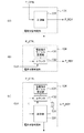
図1は、本発明の実施形態1に係る半導体集積回路100の電源制御対象部101とそのリセット構成の概略を示すブロック図である。電源制御対象部101は電源ドメインや電圧ドメインと呼称されることが多い。ここで、電源ドメインとは同一(複数組みであってもよい)の電力制御素子(例えば、PMOSスイッチ、FET)によって電源の供給を止められる集積回路上の一領域を示し、チップ上の漏れ電流(リーク電流)を抑制するためのものである。なお、電源ドメインとはこの定義を満たす回路ブロックや、機能モジュール、集積回路、サブシステムなどであってもよい。また、1つの電源ドメインに複数の機能モジュールやサブシステムを包含させてもよい。
FIG. 1 is a block diagram showing an outline of a power
図1において、電源制御対象部101へ入力される電源電圧となる電源Vddaは、電源スイッチなどの電源制御部102を介して電源Vddに接続されている。アプリケーションプログラムやユーザによる外部電源スイッチの操作に応じて発行される電源制御指示(P_CMDと表記する)に基づいて、電源制御部102を操作するための操作指示(P_CTRLと表記する)を電源制御指示部103が発行する。
In FIG. 1, a power supply Vdda that is a power supply voltage input to the power supply
電源状態判定部104は、電源制御対象部101の電源Vddaの状態を検出し、電源対象部101が安定して動作可能な電源電圧で有れば、そのことを示すパワーレディ信号(P_RDYと表記する)をリセット動作設定部105に送信する。リセット動作設定部105は、アクティブなパワーレディ信号を受信したことに応じて、ゲーティングクロックバッファ106に対してゲーティングを解除するクロックイネーブル信号(CLK_ENと表記する)を送信する。なお、リセット動作設定部105はクロックイネーブル信号を送信するとともに、電源制御対象部101に対して設定された期間だけリセット信号(P_RSTと表記する)を送信して初期化動作を実施する。
The power supply
なお、本明細書では初期化動作とは、電源制御対象部101を初期化するために、安定した電源電圧が供給されている電源制御対象部101に対して、クロック(CLK_Gと表記する)とアクティブなリセット信号(P_RST)とを供給し続ける動作を示すものとする。
In this specification, the initialization operation is a clock (denoted as CLK_G) for the power
なお、図1の電源制御部102は、PMOSからなる電源スイッチを用いた構成であるが、NMOSとPMOSを含む相補スイッチ等、電源電圧を制御するものであれば本発明に適用することができる。また、図1のゲーティングクロックバッファ106はOR型論理によりクロック伝搬をネゲートする構成であるが、AND型論理であってもよい。以降の説明では簡便のためPMOSとOR型論理を用いて説明する。
1 has a configuration using a power switch composed of PMOS, but can be applied to the present invention as long as it controls the power supply voltage, such as a complementary switch including NMOS and PMOS. . Further, the
なお、図1に記載の電源制御部102から電源制御対象部101に向けて記した矢印は電源Vddaの供給経路を示している。また、図1に記載の電源状態判定部104から電源制御対象部101に向けて線と丸端子で記した箇所は、電源状態判定部104が電源状態を検知する計測器により構成されている場合のセンシングの端子を示している。電源状態判定部104、リセット動作設定部105の詳細については後述する。
Note that an arrow written from the
図2は、実施形態1に係る半導体集積回路100のリセット構成に関する各種信号について電源を復帰させる際のタイミングチャートを示している。詳細には、電源制御対象部101への電源供給が停止している電源遮断期間T1、電源供給を行う電源復帰期間T2、電源が安定したことを検出した後に初期化動作を実施するリセット期間T3、さらに定常動作期間T4を順に移行する様子を示している。
FIG. 2 is a timing chart when power is restored for various signals related to the reset configuration of the semiconductor integrated
CLKは半導体集積回路100に供給されるシステムクロックである。このCLKは半導体集積回路100内のクロックジェネレータが発生させたものであってもよい。
CLK is a system clock supplied to the semiconductor integrated
P_CMD、P_CTRL、Vdda、P_RDY、CLK_EN、CLK_G、P_RSTについては図1に示す信号と対応しており、図2のチャートでデジタル信号はロー・アクティブ(負極性)として示しているが、論理回路との対応がとれていれば正極性であっても本発明を適用できる。 P_CMD, P_CTRL, Vdda, P_RDY, CLK_EN, CLK_G, and P_RST correspond to the signals shown in FIG. 1, and the digital signal is shown as low active (negative polarity) in the chart of FIG. The present invention can be applied even if it is positive polarity.
本実施形態では電源制御指示(P_CMD)が有効になって、電源復帰期間T2に遷移しても、電源電圧Vddaが安定したことを示す通知としてP_RDYが有効になるまでリセット動作設定部105はクロック制御信号(CLK_EN)を有効にはしない。本実施形態のリセット動作設定部は、電源状態判定部104がパワーレディ信号(P_RDY)を有効へ遷移させたことをトリガにしてCLK_ENを有効にして、予め設定された期間(サイクル数)だけ初期化動作を行う。
In this embodiment, even if the power supply control instruction (P_CMD) becomes valid and transitions to the power recovery period T2, the reset
以降は、実施形態1の各種構成について詳細を説明する。 Hereinafter, details of various configurations of the first embodiment will be described.
<電源状態判定部>
図3(a)〜(c)の其々は、実施形態1の電源状態判定部104の詳細を示している。
<Power status determination unit>
Each of FIGS. 3A to 3C shows details of the power supply
図3(a)は、電源制御対象部101の電圧状態を直接検知する構成である。すなわち、操作指示(P_CTRL)の入力に応じて電源電圧を計測する計測器301によって、電源制御対象部101が安定して動作する規定電圧にVddaが達したことを検出することで、電源制御対象部101の電源復帰タイミングの正確な検知が可能となる。図3に記載の電源状態判定部104から外部に向けて線と丸端子で記した箇所は、電源制御対象部101の電源Vddaの状態をセンシングする端子を示している。なお、計測器301は電流や電圧比較など、電圧と対応して変化する他の物理量を測定することで電源Vddaga安定したことを検出してもよし、CMOSトランジスタの信号の変化点を利用して電源電圧を検知してもよい。さらに、操作指示を計測開始のトリガとしなくてもよい、不図示のCPU等からの指示によって計測を開始してもよい。
FIG. 3A shows a configuration in which the voltage state of the power
図3(b)は、電源供給開始から規定電圧に復帰するまでの期間が予め分っており、この期間を計数することで、安定動作可能な電圧状態であることを検知する構成である。不図示のCPU等から電源復帰にかかる期間に相当する値(サイクル数など)を受けてカウンタ402に設定する電源復帰サイクル設定部401と、操作指示(P_CTRL)の入力に応じて、設定された電源復帰期間を計数するカウンタ402とを備える電源状態判定部104の構成を示す。なお、電源復帰サイクル設定部401は、CPU等によるレジスタ設定以外にも、予め固定値を保持する構成であっても、設定をメモリ等から読み出す構成でもよい。
FIG. 3B shows a configuration in which the period from the start of power supply to the return to the specified voltage is known in advance, and by counting this period, it is detected that the voltage state is capable of stable operation. A power supply return
図3(c)は、図3(a)の構成と図3(b)の構成とを選択的に動作できるようにした電源状態判定部104である。不図示のレジスタや外部からの入力に応じて、2つの構成を切り替えるセレクタ501をさらに備える。例えば、通常は計測器301によってVddaの状態を計測し、Vddaのふらつきが許容できない場合などにはカウンタ402を用いた構成を切り替えるように用いることができる。
FIG. 3C shows a power supply
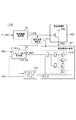
<リセット動作設定部>
図4(a)〜(c)の其々は、実施形態1のリセット動作設定部105の詳細を示している。図4(a)は、リセットに必要なサイクル数を設定するリセットサイクル設定部601と、電源状態判定部104から送信されるパワーレディ信号(P_RDY)をトリガに動作を開始するカウンタ602を備える、リセット動作設定部105を示す。リセット動作設定部105はカウンタ602でカウント(計時)を開始するとともにクロックイネーブル信号(CLK_EN)の出力を開始し、カウントが終了するとともにリセット信号(P_RST)の送信を終了する。なお、リセットサイクル設定部601は予め固定値を保持していてもよいし、不図示のCPU等によるレジスタ設定でカウント値を保持してもよいし、メモリ等からカウント値を読み出す構成であってもよい。
<Reset operation setting section>
Each of FIGS. 4A to 4C shows details of the reset
図4(b)は、図4(a)の構成に、クロックイネーブル信号やリセット信号を遅延させるカウンタ702を追加したリセット動作設定部105を示している。この構成ではパワーレディ信号の入力を受けて、予めリセット開始遅延設定部701により設定した期間(値、サイクル数)だけカウンタ702によりカウントさせ、カウンタ702のカウント中はパワーレディ信号の伝播を待機させる。カウンタ702が設定された期間カウントし終えると、クロックイネーブル信号(CLK_EN)の出力を開始し、パワーレディ信号をカウンタ602に伝播させる。その後段の構成や機能は図4(a)の構成や機能と同様なので、説明を省略する。
FIG. 4B shows a reset
図4(c)は、リセット動作設定部105を電源制御対象部101と、より同期して動作させるために信号同期化回路801を追加している。例えば、電源状態判定部104が、図3(a)、図3(c)のように電源Vddaの状態を測定する場合、パワーレディ信号は必ずしもリセット回路100に同期して入力されるとは限らない。他にも、電源状態判定部104とリセット動作設定部105とを、半導体集積回路100のレイアウトを決定する段階で同期設計することが困難であることも考えられる。なお、リセット動作設定部105からの出力信号(リセット信号、クロックイネーブル信号)に関しても同様に同期信号出力回路802、803としてフリップフロップを配置している。
In FIG. 4C, a
なお、図3(a)〜(c)の電源状態判定部104のいずれかと図4(a)〜(c)のリセット動作設定部105のいずれかを組み合わせれば、実施形態1の効果を得ることはできる。
Note that the effect of the first embodiment can be obtained by combining any one of the power supply
以上のとおり、本実施形態では図2のタイミングチャートに示す通り、電源電圧が安定してから初期化動作を開始するため、特許文献1の技術と比べて効率的に初期化動作を実施するとともに消費電力を低減させることができる。 As described above, in this embodiment, as shown in the timing chart of FIG. 2, the initialization operation is started after the power supply voltage is stabilized. Therefore, the initialization operation is performed more efficiently than the technique of Patent Document 1. Power consumption can be reduced.
<実施形態2>
本実施形態では、実施形態1の電源制御構成を、半導体集積回路100(以下、サブモジュールとして説明する)をN個(Nは2以上の整数)備える半導体集積回路900に拡張した構成について説明する。なお、本実施形態の説明に用いる図面について、実施形態1の構成と変わらない構成については同じ符号を付すと共に、機能も変わらない場合にはその説明を省略する。
<Embodiment 2>
In the present embodiment, a configuration in which the power supply control configuration of the first embodiment is extended to a semiconductor integrated
図5は、実施形態1で半導体集積回路100として説明したサブモジュール100をN個備える半導体集積回路900の概略構成を示す。CLK制御部903は、各サブモジュールに供給するクロックを個別に制御する。RS制御部904は各サブモジュールに供給するリセット信号を個別に制御する。Power制御部905は各サブモジュールに対して電源制御指示を個別に出力する。なお、本実施形態では、Power制御部905で集中制御された各サブモジュールの電源制御指示(P_CMD)を各サブモジュールの電源制御指示部103に送信する形態を取っているが、Power制御部905と各サブモジュールの電源制御指示部103の機能を併せた一つのブロックとして実装する構成でもよい。この場合、Power制御部905と各サブモジュールの電源制御指示部103を併せたブロックから直接、操作指示(P_CTRL)が電源制御部102と電源状態判定部104に送信する構成となる。
FIG. 5 shows a schematic configuration of a semiconductor integrated
図5に示す構成ではサブモジュールのすくなくとも1つがCPU906、ROM907、RAM908を備えているが、各サブモジュールでCPU906、ROM907、RAM908などを分担して備えていてもよい。設定部901は各サブモジュールの備える各種カウンタや電源復帰サイクル設定部401に電源復帰などに関わるパラメータを設定する。
In the configuration shown in FIG. 5, at least one of the sub modules includes the
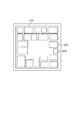
図6は、図5に示した半導体集積回路900について、20個の電源制御対象部101と電源制御指示部905を配置するフロアプランの概略を示している。図6に図示するように、電源制御対象部101によっては大きさや配置が異なっている。この図ではリセット動作設定部105や電源状態判定部104、ゲーティングクロックバッファ106については省略している。本実施形態では電源制御対象部101への電源供給を制御する際に、電源制御対象部101を複数のパワースイッチによって囲んでいるので、電源制御対象部101を囲む枠に沿って電源制御部102が配置される。また、本実施形態では基本的に電源制御領域は集積回路上で領域が重ならないように構成される。
FIG. 6 shows an outline of a floor plan in which 20 power
ここで、図6の構成について、電源制御指示部103や電源状態判定部104やリセット動作設定部105を電源制御対象部101やゲーティングクロックバッファ106と同期させることが困難になることが予想される。そのような場合に備えて、図7(a)や図7(b)に示すように電源制御対象部101やゲーティングクロックバッファ106に同期化の機構を設けてもよい。図7(a)に示す構成では、ゲーティングクロックバッファ106の前段に信号同期化回路1102を設け、クロックイネーブル信号(CLK_EN1)とリセット動作設定部105との同期性を高めることができる。なお、ここで中継レジスタ1101は電源制御対象部101内部にリセット信号(P_RST1)を分配する。図7(b)に示す構成では、電源制御対象部101の内部にリセット信号を分配する中継レジスタ1101を設け、その前段に信号同期化回路1201を設けている。
6, it is expected that it is difficult to synchronize the power
以上のとおり、本実施形態では複数の電源制御構成を好ましく制御することができる。 As described above, in the present embodiment, a plurality of power supply control configurations can be preferably controlled.
<実施形態3>
本実施形態では、実施形態1、2の構成について電源ドメイン制御とクロックドメイン制御(クロック遮断による省電力制御)を両立できるように拡張した構成について説明する。クロックドメイン制御は、クロックを遮断しダイナミック電流を削減する省電力方法である。なお、本実施形態の説明に用いる図面について、実施形態1、2の構成と変わらない構成については同じ符号を付すと共に、機能も変わらない場合にはその説明を省略する。
<Embodiment 3>
In this embodiment, a configuration in which the configurations of the first and second embodiments are extended so that both power domain control and clock domain control (power saving control by clock cutoff) can be achieved will be described. Clock domain control is a power saving method that cuts off the clock and reduces dynamic current. In the drawings used for the description of the present embodiment, the same reference numerals are given to configurations that are not different from the configurations of the first and second embodiments, and descriptions thereof are omitted when the functions are not changed.
図8は、実施形態1、実施形態2のリセット動作設定部105にクロックドメイン制御用の第2クロックイネーブル信号(EX_CENと表記する)を入力し、クロックドメイン制御ができるようにしたものである。なお、本実施形態の説明ではCLK_ENを第1クロックイネーブル信号と呼称する。ここで、第2クロックイネーブル信号は、動作状態にある電源制御対象部101へのクロック供給の遮断の有無を切り替えるためのものであるが、初期化動作の期間は電源遮断対象101へのクロック供給に影響しないように構成する必要がある。
In FIG. 8, a second clock enable signal (denoted as EX_CEN) for clock domain control is input to the reset
図9は、本実施形態のリセット動作設定部105の構成を示したブロック図である。図9の構成では初期化動作のためのクロック供給制御に影響を与えないように第2クロックイネーブル信号を合成し、第1クロックイネーブル信号を出力するイネーブル合成部1401を追加している。なお、カウンタ602はイネーブル合成部1401に対して内部信号(R_CNT)を供給する。この構成によって、電源ドメインについて動作状態となっている電源制御対象部101へのクロックを遮断することによる省電力制御を効率的に実施しつつ、初期化動作のためクロック供給を遮断しないようにすることができる。
FIG. 9 is a block diagram showing a configuration of the reset
図10(a)、図10(b)は、図9に示したリセット動作設定部105に関する各種信号のタイミングチャート(EX_CEN、CLK_ENは負極性)を示す。
10A and 10B are timing charts of various signals related to the reset
図10(a)は、電源復帰後のリセット期間T3の間に、リセット動作設定部105に入力される第2クロックイネーブル信号(EX_CEN)が有効にされた場合を示している。図10(a)に示すように、図9の構成では電源復帰に伴う初期化動作のための第1クロックイネーブル信号(CLK_EN)を設定された期間だけ電源制御対象部101へクロック供給するようにしている。従って、リセット期間T3終了後に電源制御対象部101は直ちに通常動作が可能である。
FIG. 10A shows a case where the second clock enable signal (EX_CEN) input to the reset
図10(b)は、電源復帰後のリセット期間T3が終了した後で第2クロックイネーブル信号(EX_CEN)が有効にされた場合を示している。すなわち、図10(b)に示すように、リセット期間T3終了後であれば、第2クロックイネーブル信号によって直ぐに電源制御対象部101へのクロックを停止し省電力が可能である。
FIG. 10B shows a case where the second clock enable signal (EX_CEN) is validated after the reset period T3 after the power is restored. That is, as shown in FIG. 10B, if the reset period T3 is over, the clock to the power
以上のとおり、本実施形態では電源制御対象部101への初期化動作に影響を与えない様にクロックドメイン制御をして消費電力を低減させる制御をすることができる。すなわち、本実施形態によれば電源ドメイン制御とクロックドメイン制御とを効率的に両立させることができる。
As described above, in this embodiment, it is possible to perform control to reduce power consumption by performing clock domain control so as not to affect the initialization operation to the power
<実施形態3の変形例1>
本実施形態では、実施形態1〜3の構成について電源ドメイン制御と電源ドメイン制御に関わらないリセット制御とを両立させるように拡張した構成について説明する。なお、本実施形態の説明に用いる図面について、実施形態1、2の構成と変わらない構成については同じ符号を付すと共に、機能も変わらない場合にはその説明を省略する。
<Modification 1 of Embodiment 3>
In the present embodiment, a configuration in which the configurations of the first to third embodiments are extended so as to achieve both power domain control and reset control not related to power domain control will be described. In the drawings used for the description of the present embodiment, the same reference numerals are given to configurations that are not different from the configurations of the first and second embodiments, and descriptions thereof are omitted when the functions are not changed.
図11(a)は、リセット動作設定部105に外部からリセット信号が入力される構成を示している。図11(a)において、リセット動作設定部105は、電源状態判定部104からのパワーレディ信号以外に、外部からのリセット信号である外部リセット信号(RST)に基づいてリセットの動作を行う。ここで、外部リセット信号は、電源制御対象部101へのリセットを制御するためのものであるが、電源を復帰させた際の初期化動作のための電源遮断対象101へのリセット信号の供給には影響しないように構成する必要がある。
FIG. 11A shows a configuration in which a reset signal is input to the reset
図11(b)は、本実施形態のリセット動作設定部105の構成を示したブロック図である。図11(b)に示す構成では、図4(a)のリセット動作設定部105に初期化動作のためのリセット信号の供給制御に影響を与えないように外部リセット信号を合成し、第1クロックイネーブル信号を出力するリセット合成部1801を追加している。
FIG. 11B is a block diagram showing a configuration of the reset
図12(a),図12(b)は、図11(b)に示したリセット動作設定部105に関する各種信号のタイミングチャート(RST、CLK_EN、P_RSTは負極性)を示す。図12(a),図12(b)は図10(a),図10(b)の第2クロックイネーブル信号(EX_CEN)を反転させ外部リセット信号(RST)とした様なタイミングチャートとなっているので、詳細な説明は省略する。
12A and 12B are timing charts of various signals related to the reset
以上のとおり、本実施形態では電源ドメイン制御と電源ドメイン制御に関わらないリセット制御とを効率的に両立させることができる。 As described above, in the present embodiment, it is possible to efficiently achieve both power domain control and reset control not related to power domain control.
<実施形態3の変形例2>
本実施形態では、実施形態3の変形例1の電源制御対象部101にリセット伝播機構を設けるように拡張した構成について説明する。なお、本実施形態の説明に用いる図面について、実施形態1、2、3の構成と変わらない構成については同じ符号を付すと共に、機能も変わらない場合にはその説明を省略する。
<Modification 2 of Embodiment 3>
In the present embodiment, a configuration in which the reset propagation mechanism is provided in the power
図13に示す電源制御対象部101は、リセット信号を伝播させるために、カスケード状に階層的に分配されている複数のレジスタを有する。図13に示す構成では、電源制御対象部101の内部でリセット信号を多数のレジスタに分配させる際に、分配されたリセット信号を安定させるために、リセット信号の伝達経路に伝搬回路2101を配置している。図13の電源制御対象部101は、3段のレジスタによるカスケード分配の後、リセット対象のレジスタ類に接続されている。この構成によると、リセット開始後、4サイクル目でリセット対象のレジスタのリセットが完了する。すなわち、リセット対象のレジスタを含めてk段(複数段)のカスケード分配のレジスタ(図示しているものはk−1段)を備える電源制御対象部101について、初期化動作中にレジスタの段数に対応する回数(k回)の立ち上がりエッジを有するクロック信号CLK_Gを電源制御対象部101へ送信することで初期化動作を実現することができる。
The power supply
図14は、図13に示す構成において電源を復旧させる際の各種信号のタイミングチャートを示す。 FIG. 14 is a timing chart of various signals when the power is restored in the configuration shown in FIG.
図14は、4つの立ち上がりエッジを持つクロック信号CLK_Gをリセット期間T3の最初に送信している。このような動作はリセット動作設定部105内部のリセットサイクル数設定部601に設定することで実現できる。
In FIG. 14, the clock signal CLK_G having four rising edges is transmitted at the beginning of the reset period T3. Such an operation can be realized by setting in the reset cycle
なお、図11に示す外部からのリセット信号を用いた構成を説明したが、図8に示す外部からのクロックイネーブル信号を用いた構成でも同様に本実施形態を実現できる。 Although the configuration using the reset signal from the outside shown in FIG. 11 has been described, the present embodiment can be similarly realized by the configuration using the clock enable signal from the outside shown in FIG.
以上のとおり、本実施形態では電源制御対象部101にカスケード分配を備える際にカスケード分配に対応して効率的に初期化動作のためのクロックを供給するため、初期化動作中の消費電力をさらに低減することができる。
As described above, in the present embodiment, when the power supply
<実施形態4>
本実施形態では、実施形態1〜3の構成について初期化動作中に電源制御対象部101に供給するクロックを分周する構成を設けるように拡張した構成について説明する。
<Embodiment 4>
In the present embodiment, a configuration in which the configuration of the first to third embodiments is expanded to provide a configuration for dividing the clock supplied to the power
図15(a)は、クロック周波数を落として動作率を下げるリセット動作設定部105の構成を示している。図15(a)の構成では、リセット動作設定部105の分周回路2401がクロック信号CLKを低い周波数に変換する。次に、分周回路2401は変換したクロック信号CLKとエッジの揃ったクロック信号CLK_DIVを、カウンタ602とカウンタ2402とへ個別に送信する。カウンタ2402は電源制御対象部101に入力されるクロック信号CLK_Gの立ち上がりエッジをクロックゲーティングで間引いて間欠クロックを発生させるための信号CLK_ENを作る。
FIG. 15A shows the configuration of the reset
図15(a)は、図15(b)のリセット動作設定部105を用いて電源制御対象部101の電源を復旧させる際の各種信号のタイミングチャートを示している。カウンタ2402による間引き動作により分周されたクロック信号CLK_Gによって初期化動作(リセット期間T3)をした後で定常動作期間T4へと移行している。
FIG. 15A shows a timing chart of various signals when the power supply of the power
以上のとおり、本実施形態では初期化動作中に電源制御対象部101へ供給するクロックを分周することで、初期化動作中の消費電力をさらに低減させることができる。
As described above, in the present embodiment, by dividing the clock supplied to the power
上述の各実施形態では説明の簡便のため、実施形態毎の図面を用意して説明したが、複数の実施形態を組み合わせても本発明を実施できる。その場合、各実施形態の効果に対応する複数の課題を解決していることに相当する。また、上述の各実施形態では半導体集積回路を用いて説明したが、本発明はクロックゲーティングが可能なハードワイヤードロジックを備える情報処理装置に適用することもできる。 In each of the above-described embodiments, the drawings for each embodiment have been prepared and described for the sake of simplicity of explanation. However, the present invention can also be implemented by combining a plurality of embodiments. In this case, this corresponds to solving a plurality of problems corresponding to the effects of the embodiments. In each of the above-described embodiments, the semiconductor integrated circuit has been described. However, the present invention can also be applied to an information processing apparatus including a hard wired logic capable of clock gating.
上述の実施形態では、複数の電源ドメインを並列に備える場合についてだけ例示しているが、電源ドメイン1つの内部にさらに図5のような構成を設けて複数の電源ドメインを階層構造にしてもよい。電源ドメインの数が増加すると、一括して管理することが困難なことがある、そのような場合、上流の階層では大雑把な機能グループについて設定されている電源ドメインを制御させ、下流の階層では詳細な機能について電源ドメインを制御させ、分散的に電源ドメインの制御をすることができる。 In the above-described embodiment, only the case where a plurality of power supply domains are provided in parallel is illustrated, but the configuration shown in FIG. 5 may be further provided inside one power supply domain to form a plurality of power supply domains in a hierarchical structure. . When the number of power domains increases, it may be difficult to manage them collectively. In such a case, the power domains set for the rough function group are controlled in the upstream hierarchy, and the details are detailed in the downstream hierarchy. The power domain can be controlled for various functions, and the power domain can be controlled in a distributed manner.
100 リセット回路
101 電源制御対象部
102 電源制御部
103 電源制御指示部
104 電源状態判定部
105 リセット動作設定部
106 ゲーティングクロックバッファ
DESCRIPTION OF
Claims (12)
前記電源制御対象部に供給する電源を制御する電源制御手段と、
前記電源制御手段によって前記電源制御対象部へ供給される電源の電圧を計測し、計測された前記電圧が前記電源制御対象部を動作させるための規定電圧まで達したかを検出する検出手段と、
計測された前記電圧が前記規定電圧まで達したことが検出された場合、前記電源制御対象部を初期化するためのクロック供給が開始されるように制御する初期化手段とを有することを特徴とする半導体集積回路。 A power control target unit for controlling the power to be supplied; and
Power control means for controlling the power supplied to the power control target unit;
Detecting means for measuring the voltage of the power supplied to the power control target unit by the power control means, and detecting whether the measured voltage has reached a specified voltage for operating the power control target unit;
Initializing means for performing control so that clock supply for initializing the power control target unit is started when it is detected that the measured voltage has reached the specified voltage. A semiconductor integrated circuit.
前記電源制御対象部に供給する電源を制御する電源制御手段と、
前記電源制御手段によって前記電源制御対象部へ供給される電源の電圧が、前記電源制御対象部を動作させるための規定電圧まで達したことを検出する検出手段と、
前記検出手段の検出に基づいて前記電源制御対象部を初期化するためのクロック供給が開始されるように制御する初期化手段と、を有し、
前記初期化手段は、前記電源制御対象部に対するクロック供給を開始するためのイネーブル信号と、前記電源制御対象部に対するリセット信号とを遅延させる遅延手段とを備えることを特徴とする半導体集積回路。 A power control target unit for controlling the power to be supplied; and
Power control means for controlling the power supplied to the power control target unit;
Detecting means for detecting that the voltage of the power supplied to the power control target part by the power control means has reached a specified voltage for operating the power control target part;
Initialization means for controlling so that clock supply for initializing the power control target unit is started based on detection of the detection means,
2. The semiconductor integrated circuit according to claim 1, wherein the initialization means includes delay means for delaying an enable signal for starting clock supply to the power control target unit and a reset signal for the power control target unit.
前記電源制御対象部に供給する電源を制御する電源制御手段と、
前記電源制御手段によって前記電源制御対象部へ供給される電源の電圧が、前記電源制御対象部を動作させるための規定電圧まで達したことを検出する検出手段と、
前記検出手段の検出に基づいて前記電源制御対象部を初期化するためのクロック供給が開始されるように制御する初期化手段と、を有し、
前記初期化手段は、前記電源制御対象部に対するクロック供給を開始するためのイネーブル信号と、前記電源制御対象部に対するリセット信号とを同期させる同期手段とを備えることを特徴とする半導体集積回路。 A power control target unit for controlling the power to be supplied; and
Power control means for controlling the power supplied to the power control target unit;
Detecting means for detecting that the voltage of the power supplied to the power control target part by the power control means has reached a specified voltage for operating the power control target part;
Initialization means for controlling so that clock supply for initializing the power control target unit is started based on detection of the detection means,
The semiconductor integrated circuit according to claim 1, wherein the initialization unit includes a synchronization unit that synchronizes an enable signal for starting clock supply to the power control target unit and a reset signal for the power control target unit.
前記電源制御対象部に供給する電源を制御する電源制御手段と、
前記電源制御手段によって前記電源制御対象部へ供給される電源の電圧を計測し、計測された前記電圧が前記電源制御対象部を動作させるための規定電圧まで達したかを検出する検出手段と、
計測された前記電圧が前記規定電圧まで達したことが検出された場合、前記電源制御対象部を初期化するためのクロック供給が開始されるように制御する初期化手段とを有することを特徴とする情報処理装置。 A power control target unit for controlling the power to be supplied; and
Power control means for controlling the power supplied to the power control target unit;
Detecting means for measuring the voltage of the power supplied to the power control target unit by the power control means, and detecting whether the measured voltage has reached a specified voltage for operating the power control target unit;
Initializing means for performing control so that clock supply for initializing the power control target unit is started when it is detected that the measured voltage has reached the specified voltage. Information processing apparatus.
Priority Applications (2)
| Application Number | Priority Date | Filing Date | Title |
|---|---|---|---|
| JP2012129885A JP6103825B2 (en) | 2012-06-07 | 2012-06-07 | Semiconductor integrated circuit, information processing device |
| US13/909,995 US9235255B2 (en) | 2012-06-07 | 2013-06-04 | Semiconductor integrated circuit and information processing apparatus |
Applications Claiming Priority (1)
| Application Number | Priority Date | Filing Date | Title |
|---|---|---|---|
| JP2012129885A JP6103825B2 (en) | 2012-06-07 | 2012-06-07 | Semiconductor integrated circuit, information processing device |
Publications (3)
| Publication Number | Publication Date |
|---|---|
| JP2013254376A JP2013254376A (en) | 2013-12-19 |
| JP2013254376A5 JP2013254376A5 (en) | 2015-07-09 |
| JP6103825B2 true JP6103825B2 (en) | 2017-03-29 |
Family
ID=49716267
Family Applications (1)
| Application Number | Title | Priority Date | Filing Date |
|---|---|---|---|
| JP2012129885A Active JP6103825B2 (en) | 2012-06-07 | 2012-06-07 | Semiconductor integrated circuit, information processing device |
Country Status (2)
| Country | Link |
|---|---|
| US (1) | US9235255B2 (en) |
| JP (1) | JP6103825B2 (en) |
Families Citing this family (7)
| Publication number | Priority date | Publication date | Assignee | Title |
|---|---|---|---|---|
| US8786332B1 (en) * | 2013-01-17 | 2014-07-22 | Apple Inc. | Reset extender for divided clock domains |
| CN104679439B (en) * | 2013-11-29 | 2018-06-26 | 英业达科技有限公司 | Data access management device and method |
| JP6582435B2 (en) * | 2015-02-24 | 2019-10-02 | セイコーエプソン株式会社 | Integrated circuit device and electronic apparatus |
| JP6562745B2 (en) * | 2015-07-16 | 2019-08-21 | キヤノン株式会社 | Photoelectric conversion device, image reading device, and image forming device |
| US10545556B2 (en) * | 2017-05-10 | 2020-01-28 | Texas Instruments Incorporated | Fine-grained dynamic power and clock-gating control |
| JP7087509B2 (en) * | 2018-03-19 | 2022-06-21 | 富士フイルムビジネスイノベーション株式会社 | Information processing equipment and circuit equipment |
| JP2023040972A (en) * | 2021-09-10 | 2023-03-23 | 国立大学法人東北大学 | Semiconductor circuit device and logic circuit design support device |
Family Cites Families (12)
| Publication number | Priority date | Publication date | Assignee | Title |
|---|---|---|---|---|
| US5801561A (en) * | 1995-05-01 | 1998-09-01 | Intel Corporation | Power-on initializing circuit |
| JP3201365B2 (en) * | 1998-11-30 | 2001-08-20 | 日本電気株式会社 | Power-on circuit for built-in IC |
| JP3437174B2 (en) * | 2001-04-12 | 2003-08-18 | 沖電気工業株式会社 | Power saving integrated circuit and control method of power saving integrated circuit |
| US7174543B2 (en) * | 2001-08-29 | 2007-02-06 | Analog Devices, Inc. | High-speed program tracing |
| KR20050085962A (en) * | 2003-01-13 | 2005-08-29 | 에이알엠 리미티드 | Data processing performance control |
| KR101136036B1 (en) * | 2003-12-24 | 2012-04-18 | 삼성전자주식회사 | Processor system and method for reducing power consumption in idle mode |
| KR100571651B1 (en) * | 2003-12-29 | 2006-04-17 | 주식회사 하이닉스반도체 | Control circuit for escaping power-down mode confidentially |
| JP4341500B2 (en) * | 2004-08-09 | 2009-10-07 | セイコーエプソン株式会社 | Information processing apparatus and power-on method |
| JP2007233718A (en) * | 2006-03-01 | 2007-09-13 | Canon Inc | Control device and semiconductor integrated circuit |
| JP4908983B2 (en) * | 2006-09-12 | 2012-04-04 | パナソニック株式会社 | Microcontrollers and related technologies |
| US8347132B2 (en) * | 2009-01-07 | 2013-01-01 | Taiwan Semiconductor Manufacturing Company, Ltd. | System and method for reducing processor power consumption |
| CN101944527B (en) * | 2009-07-08 | 2012-11-21 | 炬才微电子(深圳)有限公司 | Integrated circuit and standby controlling method thereof |
-
2012
- 2012-06-07 JP JP2012129885A patent/JP6103825B2/en active Active
-
2013
- 2013-06-04 US US13/909,995 patent/US9235255B2/en active Active
Also Published As
| Publication number | Publication date |
|---|---|
| JP2013254376A (en) | 2013-12-19 |
| US20130332758A1 (en) | 2013-12-12 |
| US9235255B2 (en) | 2016-01-12 |
Similar Documents
| Publication | Publication Date | Title |
|---|---|---|
| JP6103825B2 (en) | Semiconductor integrated circuit, information processing device | |
| JP5734518B2 (en) | Multi-clock real-time counter | |
| KR102161083B1 (en) | Semiconduct memory device | |
| JP2009147221A (en) | Semiconductor device | |
| JP2010108217A (en) | Memory interface and method of operating the same | |
| US9740454B2 (en) | Crossing pipelined data between circuitry in different clock domains | |
| KR20200038555A (en) | Devices and methods for detecting loop count in delay-fixed loop | |
| EP2707955B1 (en) | Synchronized output of multiple ring oscillators | |
| US6078202A (en) | Semiconductor device having portions that operate at different frequencies, and method of designing the device | |
| US8493108B2 (en) | Synchronizer with high reliability | |
| US9367081B2 (en) | Method for synchronizing independent clock signals | |
| JP2015035241A (en) | Semiconductor device | |
| KR100986534B1 (en) | Multimode?uniform?latency clock generation circuit | |
| US8395946B2 (en) | Data access apparatus and associated method for accessing data using internally generated clocks | |
| JP2008102619A (en) | Circuit generation system, circuit generation method and circuit generation program | |
| US9354658B2 (en) | Method for asynchronous gating of signals between clock domains | |
| JP2005518685A (en) | Method and apparatus for clock circuit | |
| JP2006332919A (en) | Semiconductor integrated circuit | |
| US9304531B2 (en) | Dynamically scaling voltage/frequency | |
| JP2009009544A (en) | Clock supply circuit and clock supply method | |
| JP2004258888A (en) | Semiconductor integrated circuit | |
| KR20130142744A (en) | Reset signal generating device | |
| US8499188B2 (en) | Processing device for determining whether to output a first data using a first clock signal or a second data using delay from the first clock signal according to a control signal | |
| US20230129642A1 (en) | On-die power supply monitor design | |
| JP2001216047A (en) | Delay adjusting circuit |
Legal Events
| Date | Code | Title | Description |
|---|---|---|---|
| A521 | Request for written amendment filed |
Free format text: JAPANESE INTERMEDIATE CODE: A523 Effective date: 20150525 |
|
| A621 | Written request for application examination |
Free format text: JAPANESE INTERMEDIATE CODE: A621 Effective date: 20150525 |
|
| A977 | Report on retrieval |
Free format text: JAPANESE INTERMEDIATE CODE: A971007 Effective date: 20160502 |
|
| A131 | Notification of reasons for refusal |
Free format text: JAPANESE INTERMEDIATE CODE: A131 Effective date: 20160517 |
|
| A521 | Request for written amendment filed |
Free format text: JAPANESE INTERMEDIATE CODE: A523 Effective date: 20160701 |
|
| A131 | Notification of reasons for refusal |
Free format text: JAPANESE INTERMEDIATE CODE: A131 Effective date: 20161122 |
|
| A521 | Request for written amendment filed |
Free format text: JAPANESE INTERMEDIATE CODE: A523 Effective date: 20170119 |
|
| TRDD | Decision of grant or rejection written | ||
| A01 | Written decision to grant a patent or to grant a registration (utility model) |
Free format text: JAPANESE INTERMEDIATE CODE: A01 Effective date: 20170131 |
|
| A61 | First payment of annual fees (during grant procedure) |
Free format text: JAPANESE INTERMEDIATE CODE: A61 Effective date: 20170228 |
|
| R151 | Written notification of patent or utility model registration |
Ref document number: 6103825 Country of ref document: JP Free format text: JAPANESE INTERMEDIATE CODE: R151 |