JP6098429B2 - Arithmetic processing device and control method of arithmetic processing device - Google Patents
Arithmetic processing device and control method of arithmetic processing device Download PDFInfo
- Publication number
- JP6098429B2 JP6098429B2 JP2013167781A JP2013167781A JP6098429B2 JP 6098429 B2 JP6098429 B2 JP 6098429B2 JP 2013167781 A JP2013167781 A JP 2013167781A JP 2013167781 A JP2013167781 A JP 2013167781A JP 6098429 B2 JP6098429 B2 JP 6098429B2
- Authority
- JP
- Japan
- Prior art keywords
- instruction
- signal
- branch instruction
- completion
- branch
- Prior art date
- Legal status (The legal status is an assumption and is not a legal conclusion. Google has not performed a legal analysis and makes no representation as to the accuracy of the status listed.)
- Expired - Fee Related
Links
- 238000000034 method Methods 0.000 title claims description 35
- 230000008569 process Effects 0.000 claims description 29
- 230000004044 response Effects 0.000 claims description 3
- 230000001737 promoting effect Effects 0.000 claims description 2
- 230000004048 modification Effects 0.000 description 33
- 238000012986 modification Methods 0.000 description 33
- 230000007274 generation of a signal involved in cell-cell signaling Effects 0.000 description 32
- 230000001629 suppression Effects 0.000 description 27
- 230000000052 comparative effect Effects 0.000 description 21
- 238000010586 diagram Methods 0.000 description 21
- 230000001133 acceleration Effects 0.000 description 15
- 230000006870 function Effects 0.000 description 12
- 230000005764 inhibitory process Effects 0.000 description 9
- 230000015654 memory Effects 0.000 description 4
- 230000007246 mechanism Effects 0.000 description 3
- 230000002401 inhibitory effect Effects 0.000 description 1
- 239000000463 material Substances 0.000 description 1
Images


Classifications
-
- G—PHYSICS
- G06—COMPUTING; CALCULATING OR COUNTING
- G06F—ELECTRIC DIGITAL DATA PROCESSING
- G06F9/00—Arrangements for program control, e.g. control units
- G06F9/06—Arrangements for program control, e.g. control units using stored programs, i.e. using an internal store of processing equipment to receive or retain programs
- G06F9/30—Arrangements for executing machine instructions, e.g. instruction decode
- G06F9/38—Concurrent instruction execution, e.g. pipeline or look ahead
- G06F9/3802—Instruction prefetching
- G06F9/3804—Instruction prefetching for branches, e.g. hedging, branch folding
-
- G—PHYSICS
- G06—COMPUTING; CALCULATING OR COUNTING
- G06F—ELECTRIC DIGITAL DATA PROCESSING
- G06F9/00—Arrangements for program control, e.g. control units
- G06F9/06—Arrangements for program control, e.g. control units using stored programs, i.e. using an internal store of processing equipment to receive or retain programs
- G06F9/30—Arrangements for executing machine instructions, e.g. instruction decode
- G06F9/30003—Arrangements for executing specific machine instructions
- G06F9/30007—Arrangements for executing specific machine instructions to perform operations on data operands
- G06F9/3001—Arithmetic instructions
-
- G—PHYSICS
- G06—COMPUTING; CALCULATING OR COUNTING
- G06F—ELECTRIC DIGITAL DATA PROCESSING
- G06F9/00—Arrangements for program control, e.g. control units
- G06F9/06—Arrangements for program control, e.g. control units using stored programs, i.e. using an internal store of processing equipment to receive or retain programs
- G06F9/30—Arrangements for executing machine instructions, e.g. instruction decode
- G06F9/30003—Arrangements for executing specific machine instructions
- G06F9/3005—Arrangements for executing specific machine instructions to perform operations for flow control
- G06F9/30058—Conditional branch instructions
Landscapes
- Engineering & Computer Science (AREA)
- Software Systems (AREA)
- Theoretical Computer Science (AREA)
- Physics & Mathematics (AREA)
- General Physics & Mathematics (AREA)
- General Engineering & Computer Science (AREA)
- Computational Mathematics (AREA)
- Mathematical Analysis (AREA)
- Mathematical Optimization (AREA)
- Pure & Applied Mathematics (AREA)
- Advance Control (AREA)
- Executing Machine-Instructions (AREA)
Description
本案は、演算処理装置及び演算処理装置の制御方法に関する。 The present invention relates to an arithmetic processing device and a control method for the arithmetic processing device.
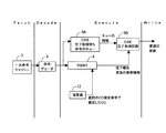
図1は、スーパースカラプロセッサの構成を例示する図である。図1を参照して、スーパースカラプロセッサの構成を説明する。図1で例示するスーパースカラプロセッサは、命令フェッチアドレスを生成する命令フェッチアドレス生成器1、分岐命令の分岐予測を行う分岐予測機構2、命令をキャッシュする一次命令キャッシュ3、フェッチされた命令を解読する命令デコーダ4、解読された命令を蓄積するリザベーションステーション(RSA5、RSE6、RSF7、RSBR8)、命令の完了処理を行うCommit Stack Entry(CSE)9、オペランドアドレスを生成するオペランドアドレス生成器10、データを格納する一次データキャッシュ11、解読された命令を実行する演算器12、演算の実行結果を格納する更新バッファ(固定小数点更新バッファ13、浮動小数点更新バッファ14)、演算の実行時に使用するレジスタ(固定小数点レジスタ15、浮動小数点レジスタ16)、命令のアドレスを保持するプログラムカウンタ(NEXT Program Counter(NEXT PC)17、Program Counter(PC)18)、条件判断に用いられるCondition Codeを格納するCondition Code(CC)レジスタ19、を有する。
FIG. 1 is a diagram illustrating a configuration of a superscalar processor. The configuration of the superscalar processor will be described with reference to FIG. The superscalar processor illustrated in FIG. 1 includes an instruction
図1のプロセッサにおける、命令の実行は以下のように例示される。プログラムの実行順序にしたがって一次命令キャッシュ3から命令がフェッチされる。フェッチされた命令は命令デコーダ4によって解読される。命令デコーダ4によって解読された命令はリザベーションステーションと呼ばれるキュー構造のストレージに蓄積される。リザベーションステーションは、命令の種類毎に用意される。固定小数点計算用のReservation Station for Execution(RSE)6、分岐命令用のReservation Station for Branch(RSBR)8等はリザベーションステーションの例示である。リザベーションステーションに蓄積された命令は、命令実行の準備が整ったものからアウトオブオーダーで実行される。
Instruction execution in the processor of FIG. 1 is illustrated as follows. Instructions are fetched from the
命令デコーダ4で解読された命令は、例えば、解読された順番にしたがって、Instruction Identification(IID)が割り振られる。IIDとは、命令を識別する識別子の例示である。IIDが割り振られた命令は、IIDが割り振られた順番にしたがってCSE9に送られる。CSE9は、命令の完了処理を行う回路の例示である。CSE9は命令デコーダ4で解読された命
令を命令の実行順に蓄積するキュー構造のストレージと、完了処理回路とを有する。CSE
9の完了処理回路は、RSBR8や演算器12、一次データキャッシュ11等から各処理の完了報告を受け取る。CSE9の完了処理回路は、その受け取った完了報告と、キューに蓄積
された情報を基に、命令完了の処理を行う。この命令完了の処理をCOMMITという。命令デコーダ4で解読された命令はCSE9のキューに蓄積される。CSE9のキューに蓄積された命令は、命令処理完了の報告を待つ。各リザベーションステーションに蓄積され、アウトオブオーダーで実行された命令の完了報告は、CSE9に送られる。CSE9の完了処理回路は、CSE9のキューに蓄積された完了報告待ちの命令の中から完了報告に対応する命令を、プ
ログラム本来の実行順序にしたがってCOMMITする。命令がCOMMITされると、資源の更新が行われる。
Instructions decoded by the
The
図2は、分岐命令の処理を例示する図である。図2を参照して、分岐命令の処理を説明する。一次命令キャッシュ3から命令がフェッチされる。フェッチされた命令は、命令デコーダ4で解読される。解読された命令はIIDが割り振られる。IIDが割り振られた命令は、CSE9の完了処理待ち命令のキュー9A(以下、CSE9のキュー9A)に蓄積される。CSE9のキュー9Aは、プログラムの実行順に完了処理待ちの命令の識別子が蓄積される完了
処理待ち記憶部の例示である。また、解読された結果、分岐命令であると判断された命令は、RSBR8に蓄積される。RSBR8に蓄積された分岐命令は、分岐が判断できる状態になるのを待つ。分岐命令では、Condition Code(CC)レジスタ19と呼ばれるレジスタの値によって、分岐する(TAKEN)か分岐しない(NOT TAKEN)かが確定(Resolve)する。した
がって、後続の分岐命令のResolveは、Condition Codeを変更する命令の完了を待つ。な
お、Condition Codeを変更する命令がCOMMITされた時にCCレジスタ19は更新される。しかし、CCレジスタ19が更新されてからRSBR8で分岐の判断を行うのでは時間がかかる。そこで、演算器12で計算されたCondition Codeを、演算器12からRSBR8に送ってもよい。RSBR8は演算器12から送られたCondition Codeを基に分岐判断を行えばよい。分岐判断できる状態になるとRSBR8は分岐判断を行う。RSBR8は、分岐命令の完了報告と資源の更新情報をCSE9の完了処理回路9Bに送る。資源の更新情報は、例えば、上述のTAKENやNOT TAKENが例示される。RSBR8は、分岐命令の完了を管理する分岐命令実行管理部の
例示である。CSE9の完了処理回路9BはRSBR8からの報告を受けて、CSE9のキュー9Aに蓄積された完了報告待ちの命令の中から完了報告に対応する分岐命令の完了処理を行い、資源の更新を行う。CSE9の完了処理回路9Bは、分岐命令の実行に伴う資源の更新処理を起動する完了処理部の例示である。
FIG. 2 is a diagram illustrating the processing of a branch instruction. The branch instruction processing will be described with reference to FIG. Instructions are fetched from the
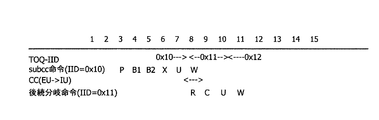
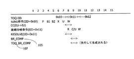
図3は、スーパースカラプロセッサにおける、Condition Codeを変更する命令から分岐命令への処理の流れを例示する図である。図3の横軸は、プロセッサのクロックを例示する。図3の縦軸は実行される命令の種類を例示する。図3では、Condition Codeを変更する命令として、subcc命令が例示される。図3のTOQ-IIDとは、CSE9のキュー9Aの先頭
になっている命令のIIDである。subcc命令(IID=0x10)は、図3で例示されるsubcc命令
のIIDが0x10であることを例示している。CC(EU->IU)は、subcc命令のCondition Codeが演算器12からRSBR8に送信されている事を例示する。EUは演算器12を例示し、IUはRSBR8を例示している。後続分岐命令(IID=0x11)は、subcc命令によって確定したCondition Codeに基づいて分岐判断を行う分岐命令のIIDが0x11であることを例示する。Resolved(IID=0x11)は、後続分岐命令(IID=0x11)の分岐の成立、不成立の確定を示す。BR_COMPは、後続分岐命令(IID=0x11)の完了を示す信号の例示である。
FIG. 3 is a diagram exemplifying a flow of processing from an instruction for changing the condition code to a branch instruction in the superscalar processor. The horizontal axis of FIG. 3 illustrates the clock of the processor. The vertical axis in FIG. 3 illustrates the type of instruction to be executed. FIG. 3 illustrates a subcc instruction as an instruction for changing the condition code. The TOQ-IID in FIG. 3 is the IID of the instruction at the head of the
subcc命令は、Priority(P)、Buffer 1(B1)、Buffer2(B2)、Execute(X)、Update(U)、Write(W)の5段のパイプラインで実行される。Pサイクルでは、リザベーショ
ンステーションは、実行待ちの命令の中から優先度の高いものを選んで、演算器12に送る。B1、B2サイクルでは、演算器12は、リザベーションステーションから送られてきた命令を実行する準備を行う。Xサイクルでは、演算器12が命令を実行する。Uサイクルでは、CSE9が命令完了の判断を行う。Wサイクルでは、各資源の更新信号がPC18などの資源の更新を行う。
The subcc instruction is executed in a five-stage pipeline of Priority (P), Buffer 1 (B1), Buffer2 (B2), Execute (X), Update (U), and Write (W). In the P cycle, the reservation station selects the instruction with high priority from the instructions waiting for execution and sends it to the
分岐命令は、Resolve(R)、Complete(C)、Update(U)、Write(W)の4段のパイプラインで実行される。Rサイクルでは、分岐命令が分岐する(TAKEN)か分岐しないか(NOT TAKEN)が確定する。Cサイクルでは、命令完了の報告がRSBR8からCSE9の完了処理回
路9Bに送られる。UサイクルでCSE9は命令完了の判断を行う。Wサイクルでは、各資源
の更新信号が資源の更新を行う。
The branch instruction is executed in a four-stage pipeline of Resolve (R), Complete (C), Update (U), and Write (W). In the R cycle, it is determined whether the branch instruction branches (TAKEN) or not (NOT TAKEN). In the C cycle, an instruction completion report is sent from the
以下、図3を参照して、各サイクルの処理を説明する。第7サイクルでは、subcc命令
のCondition Codeが、演算器12からRSBR8に送られる。第8サイクルでは、第7サイクルで送られてきたCondition Codeを基に、後続分岐命令の分岐判断が行われる。第9サイクルでは、分岐命令が完了する。分岐命令の完了を示す、BR_COMP信号105が生成され
る。第10サイクルでは、資源の更新信号が作成される。第11サイクルでは、WRITE信
号を基に、各資源の更新信号が資源の更新を行う。
Hereinafter, the processing of each cycle will be described with reference to FIG. In the seventh cycle, the condition code of the subcc instruction is sent from the
CSE9は、分岐命令を完了するため、Condition Codeの確定を待つ。Condition Codeは
、他の命令の実行結果等によって確定する。そのため、分岐命令は他の命令との依存関係が生じやすい。したがって、分岐命令は完了待ちの状態になりやすい。その結果として、プロセッサの性能が低下する場合がある。
The
そこで、本案では分岐命令の完了を高速化する事を課題とする。 Therefore, in this proposal, it is an object to speed up the completion of the branch instruction.
そこで、本案では上記課題を解決するため、実行待ち分岐命令が蓄積され、分岐命令の分岐条件が確定すると実行される分岐命令の完了を管理する分岐命令実行管理部と、プログラムの実行順に完了処理待ちの命令の識別子が蓄積される完了処理待ち記憶部と、識別子で特定される命令の実行完了報告を分岐命令実行管理部から受けて、分岐命令の実行に伴う資源の更新処理を起動する完了処理部と、完了処理待ち記憶部の先頭に蓄積された識別子が分岐命令である場合に、分岐命令の完了報告を待たず、完了処理部による資源の更新処理を起動する促進部と、を備える演算処理装置、を開示する。 Therefore, in this proposal, in order to solve the above-described problem, branch instruction execution management units that manage completion of branch instructions that are executed when branch instructions waiting for execution are accumulated and branch conditions of branch instructions are determined, and completion processing in the order of execution of the programs Completion of waiting for completion processing waiting storage section for storing the identifier of the waiting instruction, and starting update processing of resources accompanying execution of branch instruction upon receiving execution completion report of instruction specified by identifier from branch instruction execution management section A processing unit, and a promotion unit that starts a resource update process by the completion processing unit without waiting for a branch instruction completion report when the identifier accumulated at the head of the completion processing waiting storage unit is a branch instruction. An arithmetic processing device is disclosed.
本案によれば、分岐命令の完了を高速化できる。 According to the present plan, the completion of the branch instruction can be speeded up.
以下、図面を参照して、本案で開示する各実施形態について説明する。以下の各実施形態の構成は例示であり、本案は以下で開示する実施形態の構成に限定されない。 Hereinafter, each embodiment disclosed in the present plan will be described with reference to the drawings. The configurations of the following embodiments are examples, and the present invention is not limited to the configurations of the embodiments disclosed below.
<比較例>
比較例として、分岐命令の完了報告を待って分岐命令のCOMMIT処理を行うシステムを例示する。図4は、複数のプロセッサ(CPU401、CPU402)とプロセッサに接続されたメモリ(メモリ403、メモリ404)、プロセッサと外部装置との入出力制御を行うインターコネクト制御部405を例示する図である。比較例のシステムは、例えば、図4のCPU401、CPU402に適用できる。また、比較例のシステムは、図1に例示するようなアウトオブオーダー機能及びパイプライン機能を有するスーパースカラプロセッサであってもよい。
<Comparative example>
As a comparative example, a system that performs a COMMIT process for a branch instruction after waiting for a branch instruction completion report is illustrated. FIG. 4 is a diagram illustrating a plurality of processors (
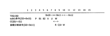
図5は、比較例のシステムにおいて、Condition Codeを変更する命令から分岐命令のCOMMIT処理への流れを例示する図である。図5の横軸は、プロセッサのクロックを例示する。図5の縦軸は実行される命令の種類を例示する。図5では、Condition Codeを変更する命令として、subcc命令が例示される。TOQ-IID、subcc命令(IID=0x10)、CC(EU->IU)
、後続分岐命令(IID=0x11)の項目の意味については、図3の場合と同様であるので、説明は省略する。
FIG. 5 is a diagram exemplifying a flow from the instruction for changing the condition code to the COMMIT process of the branch instruction in the system of the comparative example. The horizontal axis in FIG. 5 illustrates the clock of the processor. The vertical axis in FIG. 5 illustrates the types of instructions to be executed. FIG. 5 illustrates a subcc instruction as an instruction for changing the condition code. TOQ-IID, subcc instruction (IID = 0x10), CC (EU-> IU)
The meaning of the item of the subsequent branch instruction (IID = 0x11) is the same as in the case of FIG.
図5を参照して、比較例のシステムにおける、分岐命令のCOMMIT処理について説明する。第7サイクルでは、subcc命令のCondition Codeが、演算器12からRSBR8に送られる
。第8サイクルでは、第7サイクルで送られてきたCondition Codeを基に、後続分岐命令の分岐判断が行われる。第9サイクルでは、分岐命令が完了する。第10サイクルでは、資源の更新信号が作成される。第11サイクルでは、WRITE信号を基に、各資源の更新信
号が資源の更新を行う。
With reference to FIG. 5, the COMMIT processing of the branch instruction in the system of the comparative example will be described. In the seventh cycle, the condition code of the subcc instruction is sent from the
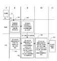
図6は、比較例のシステムにおいて、各構成要素の処理内容をサイクル毎に例示する図である。図6の横軸は、プロセッサのクロックを例示する。図6の縦軸は、処理を行う構成要素を例示する。 FIG. 6 is a diagram illustrating processing contents of each component for each cycle in the system of the comparative example. The horizontal axis in FIG. 6 illustrates the clock of the processor. The vertical axis in FIG. 6 illustrates the components that perform the processing.
図6を参照して、各構成要素が各サイクルで行う処理を説明する。第7サイクルでは、subcc命令のCondition Codeが、演算器12からRSBR8に送られる(S61)。第8サイ
クルでは、RSBR8は、RSBR8内の命令の内容による分岐条件と、Condition Codeに基づいて、分岐するかどうか判断する(S62)。CSE9のキュー9Aでは、subcc命令の完了を受け、後続の分岐命令がCSE9のキュー9Aの先頭(以下、TOQ-CSEという)となる。TOQ-CSEとなった分岐命令は、RSBR8からの完了報告であるBR_COMP信号105を待つ(S63)。第9サイクルでは、各RSBR8は、分岐判断情報からCSE9に送信する分岐判断情報を
選択する。選択された分岐判断情報を基に、RSBR8はBR_COMP信号105及びBR_TAKEN信
号を生成する(S64)。CSE9のキュー9Bでは、TOQ-CSEの分岐命令はCOMMIT処理を待つ。RSBR8からのBR_COMP信号105及びBR_TAKEN信号を受けて、CSE9の完了処理回路9Bは、TOQ_BR_COMP信号及びTOQ_BR_TAKEN信号を生成する(S65)。TOQ_BR_COMP信号を受けて、CSE9の完了処理回路9Bは分岐命令の完了を判断する。CSE9の完了処理回路9Bは、COMMIT信号であるTOQ_COMMIT信号を生成する。さらに、CSE9の完了処理回路9B
は、TOQ_BR_TAKEN信号等を基に資源の更新信号であるWRITE信号を作成する(S66)。WRITE信号を基に、各資源の更新信号が資源の更新を行う(S67)。
With reference to FIG. 6, the process which each component performs in each cycle is demonstrated. In the seventh cycle, the condition code of the subcc instruction is sent from the
Creates a WRITE signal, which is a resource update signal, based on the TOQ_BR_TAKEN signal or the like (S66). Based on the WRITE signal, the resource update signal updates the resource (S67).
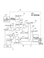
図7は、比較例におけるプロセッサのCOMMIT処理の回路を例示する図である。図7は、図1におけるCSE9とRSBR8に関する部分を例示している。図7に示すように、比較例に
おけるCSE9は、CSE9のキュー9AとCSE9の完了処理回路9Bとを有する。CSE9の完了処理回路9Bは、WRITE信号生成回路20、ラッチ24a〜24c、AND回路114a〜114c、OR回路115a、を有する。
FIG. 7 is a diagram illustrating a COMMIT processing circuit of the processor in the comparative example. FIG. 7 illustrates portions related to
図7を参照して、比較例におけるCOMMIT処理を説明する。分岐命令がTOQ-CSEの命令で
ある場合、CSE9のキュー9Aは分岐命令がTOQ-CSEの命令である事を示すTOQ_BR_USE信号104を生成する。TOQ_BR_USE信号104は、ラッチ24aに保存される。分岐命令が完了すると、RSBR8は、分岐命令の完了を示すBR_COMP信号105を生成する。RSBR8の分
岐命令がTOQ-CSEの命令である場合、TOQ_BR_COMP_SEL信号106が生成される。TOQ_BR_COMP_SEL信号106は、RSBR8で実行された分岐命令がTOQ-CSEの命令である事を示す信号である。TOQ_BR_COMP_SEL信号106は、例えば、RSBR8からBR_COMP信号105を送られる命令のIIDとTOQ-CSEの命令のIIDとが一致するとCSE9の完了処理回路9Bで生成される。AND回路114bでは、TOQ_BR_COMP_SEL信号106とRSBR8から送られたBR_COMP信号
105とのAND演算を行い、TOQ_BR_COMP信号107を生成する。TOQ_BR_COMP信号107
は、TOQ-CSEの分岐命令の完了を示す信号である。TOQ_BR_COMP信号107は、ラッチ24bに保存される。AND回路114cは、TOQ_BR_COMP_SEL信号106とRSBR8からのBR_TAKEN信号108とのAND演算を行い、TOQ_BR_TAKEN信号109を生成する。TOQ_BR_TAKEN信
号109は、TOQ-CSEの分岐命令が分岐した(TAKEN)ことを示す信号である。TOQ_BR_TAKEN信号109は、ラッチ24cに保存される。
With reference to FIG. 7, the COMMIT process in the comparative example will be described. If the branch instruction is a TOQ-CSE instruction, the
Is a signal indicating the completion of the TOQ-CSE branch instruction. The
ラッチ24bに保存されたTOQ_BR_COMP信号107によって、TOQ-CSEの分岐命令が完了した事がわかる。また、TOQ_BR_USE信号104がアサートされていない場合は、TOQ-CSE
の命令が分岐命令ではないことがわかる。そこで、OR回路115aでは、ラッチ24aに保存されたTOQ_BR_USE信号104信号をNOT演算したものとラッチ24bに保存されたTOQ_BR_COMP信号107とのOR演算を行い、TOQ_BR_COMMIT信号111を生成する。TOQ_BR_COMMIT信号111は、TOQ-CSEの分岐命令のCOMMIT処理を行ってもよい事を示す信号の例示で
ある。
The
This instruction is not a branch instruction. Therefore, the
AND回路114aは、TOQ-CSEの命令の完了を示すTOQ_COMMIT信号110を生成する。TOQ_COMMIT信号110は、TOQ_BR_COMMIT信号111、TOQ_EU_COMMIT信号112、TOQ_FCH_COMMIT信号113のAND演算で生成される。
The AND
ここで、TOQ_EU_COMMIT信号112は、プロセッサの実行ユニットで実行されるTOQ-CSEの命令のCOMMIT処理を行ってもよい事を示す信号の例示である。これ以降、プロセッサの実行ユニットで実行される命令を、EU命令という。TOQ_EU_COMMIT信号112は、例えば
、論理演算により生成される。-TOQ_EU_USE信号とTOQ_EU_COMP信号のOR演算は、TOQ_EU_COMMIT信号112を生成する論理演算の例示である。TOQ_EU_COMP信号は、TOQ-CSEのEU命
令が完了した事を示す信号の例示である。-TOQ_EU_USE信号は、TOQ-CSEの命令がEU命令ではない事を示す信号の例示である。TOQ-CSEの命令が分岐命令の場合、TOQ-CSEの命令はEU命令ではないので、-TOQ_EU_USE信号が生成される。その結果、TOQ_EU_COMMIT信号112が生成される。
Here, the
また、TOQ_FCH_COMMIT信号113は、FCHポートを利用するTOQ-CSEの命令のCOMMIT処理を行ってもよい事を示す信号の例示である。これ以降、FCHポートを利用する命令を、FCH命令という。TOQ_FCH_COMMIT信号113は、例えば、論理演算により生成される。-TOQ_FCH_USE信号とTOQ_FCH_COMP信号のOR演算は、TOQ_FCH_COMMIT信号113を生成する論理演算の例示である。TOQ_FCH_COMP信号は、TOQ-CSEのFCH命令が完了した事を示す信号の例示
である。-TOQ_FCH_USE信号は、TOQ-CSEの命令がFCH命令ではない事を示す信号の例示である。TOQ-CSEの命令が分岐命令の場合、TOQ-CSEの命令はFCH命令ではないので、-TOQ_FCH_USE信号が生成される。その結果、TOQ_FCH_COMMIT信号113が生成される。なお、LOAD
命令やSTORE命令はFCH命令の例示である。
Further, the
The command and the STORE command are examples of the FCH command.
つまり、TOQ_BR_COMMIT信号111、TOQ_EU_COMMIT信号112、TOQ_FCH_COMMIT信号113が生成されていれば、TOQ-CSEの命令が完了したことが分かる。したがって、AND回路114aは、TOQ_BR_COMMIT信号111、TOQ_EU_COMMIT信号112、TOQ_FCH_COMMIT信号
113のAND演算を行う事で、TOQ_COMMIT信号110を生成する。
That is, if the
WRITE信号生成回路20は、TOQ_COMMIT信号110とラッチ24cに保存されたTOQ_BR_TAKEN信号109を基に、資源の更新情報であるWRITE信号を生成する。WRITE信号を基に
、各資源の更新信号が資源の更新を行う。
Based on the
比較例では、RSBR8からのBR_COMP信号105を待つ事により、分岐命令の完了処理が
行われた。
In the comparative example, the branch instruction completion processing is performed by waiting for the BR_COMP signal 105 from the
<実施形態1>
比較例では、分岐命令の完了を待ってCOMMIT処理が行われた。実施形態1では、分岐命令の完了を待たずに行う分岐命令のCOMMIT処理を例示する。実施形態1のシステムは、例えば、図4のCPU401,CPU402に適用できる。また、実施形態1のシステムは、図1に例示するようなアウトオブオーダー機能及びパイプライン機能を有するスーパースカラプロセッサであってもよい。図1のプロセッサや図4のCPU401、CPU402は、演算処理装置の例示である。また、分岐命令はCondition Codeが確定してから所定のサイクルで完了する事を前提とする。実施形態1では、所定のサイクルが2サイクルの場合を例示する。
<
In the comparative example, COMMIT processing was performed after completion of the branch instruction. The first embodiment exemplifies a COMMIT process for a branch instruction that is performed without waiting for the completion of the branch instruction. The system of the first embodiment can be applied to, for example, the
図8は、実施形態1のシステムにおけるCondition Codeを変更する命令から分岐命令への処理の流れを例示する図である。図8の横軸は、プロセッサのクロックを例示する。図8の縦軸は実行される命令の種類を例示する。ここでは、Condition Codeを変更する命令として、subcc命令を例示する。TOQ_BR_COMPは、TOQ-CSEになった後続分岐命令の完了を
示す信号の例示である。TOQ-IID、subcc命令(IID=0x10)、CC(EU->IU)、後続分岐命令(IID=0x11)、RESOLVE(IID=0x11)、BR_COMPの項目の意味については、図3の場合と同様であるので、説明は省略する。
FIG. 8 is a diagram illustrating a flow of processing from an instruction for changing the condition code to a branch instruction in the system according to the first embodiment. The horizontal axis in FIG. 8 illustrates the clock of the processor. The vertical axis in FIG. 8 illustrates the type of instruction to be executed. Here, a subcc instruction is exemplified as an instruction for changing the condition code. TOQ_BR_COMP is an example of a signal indicating completion of a subsequent branch instruction that has become TOQ-CSE. The meaning of the TOQ-IID, subcc instruction (IID = 0x10), CC (EU-> IU), subsequent branch instruction (IID = 0x11), RESOLVE (IID = 0x11), and BR_COMP are the same as in FIG. Therefore, explanation is omitted.
図8を参照して、実施形態1における分岐命令のCOMMIT処理について説明する。第7サイクルでは、subcc命令のCondition Codeが、演算器12からRSBR8に送られる。第8サ
イクルでは、第7サイクルで送られてきたCondition Codeを基に後続分岐命令の分岐判断が行われる。第9サイクルでは、分岐命令が完了する。BR_COMP信号105の生成を待た
ずに、TOQ-CSEの分岐命令の完了を示すTOQ_BR_COMP信号107が生成される。分岐命令の完了に伴い、分岐命令の完了を示すBR_COMP信号105が生成される。BR_TAKEN信号10
8等を基にWRITE信号が作成される。第10サイクルでは、WRITE信号を基に、各資源の更新信号が資源の更新を行う。
With reference to FIG. 8, the COMMIT processing of the branch instruction in the first embodiment will be described. In the seventh cycle, the condition code of the subcc instruction is sent from the
A WRITE signal is created based on 8 etc. In the tenth cycle, the update signal for each resource updates the resource based on the WRITE signal.
図9は、実施形態1のCOMMIT処理の構成を例示する図である。図9は、図1に例示するプロセッサのRSBR8とCSE9の部分を例示する。実施形態1のシステムは、図9に例示す
るように、CSE9のキュー9A、CSE9の完了処理回路9B、分岐命令のCOMMITを高速化する分岐命令COMMIT高速化回路22、セレクタ25、を有する。
FIG. 9 is a diagram illustrating a configuration of COMMIT processing according to the first embodiment. FIG. 9 illustrates the
分岐命令がTOQ-CSEになると、CSE9のキュー9AはTOQ_BR_USE信号104を生成する。
分岐命令COMMIT高速化回路22は、TOQ_BR_USE信号104を受信すると、分岐命令の完了処理を開始させるSET_FORCE_BR_COMP信号101を生成する。SET_FORCE_BR_COMP信号101の生成では、分岐命令COMMIT高速化回路22は、分岐命令の完了信号であるBR_COMP信
号105を待たなくてよい。分岐命令COMMIT高速化回路22は、促進部の例示である。
When the branch instruction becomes TOQ-CSE, the
Upon receiving the
TOQ-CSEの命令が分岐命令の場合、分岐命令の前に実行されるCondition Codeを変更す
る命令は既に完了していると考えられる。そのため、分岐判断に用いるCondition Codeは確定していると考えられる。したがって、分岐命令は所定のサイクルで完了すると考えられる。実施形態1では、所定のサイクルとして、Condition Codeの確定から2サイクルで分岐命令は完了する場合を例示する。そのため、分岐命令がTOQ-CSEの命令になれば、分
岐命令は次のサイクルで完了できると考えられる。そこで、分岐命令がTOQ-CSEの命令に
なると、CSE9内での分岐命令の完了を示すTOQ_BR_COMP信号107が生成される。CSE9
の完了処理回路9BはRSBR8からの分岐命令の完了を示すBR_COMP信号105を待たなく
よい。その結果、分岐命令のCOMMITのタイミングが比較例と比べて1サイクル早くなる。そのため、比較例と同じタイミングで資源の更新情報をWRITE信号生成回路20に送信し
たのでは、WRITE信号の生成に間に合わない。そこで、実施形態1では、資源の更新情報
を1サイクル早くWRITE信号生成回路20に送信する回路が追加される。
If the TOQ-CSE instruction is a branch instruction, it is considered that the instruction for changing the condition code executed before the branch instruction has already been completed. Therefore, it is considered that the condition code used for branching determination is fixed. Therefore, the branch instruction is considered to be completed in a predetermined cycle. The first embodiment exemplifies a case where the branch instruction is completed in two cycles after the condition code is determined as the predetermined cycle. Therefore, if the branch instruction becomes a TOQ-CSE instruction, the branch instruction can be completed in the next cycle. Therefore, when the branch instruction becomes a TOQ-CSE instruction, a
The
図10は、実施形態1のシステムのCOMMIT処理の回路を例示する図である。図10は、図1におけるCSE9とRSBR8に関する部分を例示している。図10に例示するように、実
施形態1におけるCSE9は、CSE9のキュー9AとCSE9の完了処理回路9Bとを有する。CSE9の完了処理回路9Bは、WRITE信号生成回路20、ラッチ24a〜24d、AND回路114a〜114c、OR回路115a〜115bとを有する。比較例と同一の構成要素については、同一の符号を付し、その説明を省略する。
FIG. 10 is a diagram illustrating a COMMIT processing circuit of the system according to the first embodiment. FIG. 10 illustrates portions related to
図10を参照して、実施形態1のシステムのCOMMIT処理を説明する。上述の通り、分岐命令がTOQ-CSEの命令である場合、次のサイクルで分岐命令が完了すると考えられる。そ
こで、TOQ_BR_USE信号104が生成されると、OR回路115bはBR_COMP信号105を待
たずにTOQ_BR_COMP信号107を生成する。TOQ_BR_COMP信号107はラッチ24bに保存される。BR_COMP信号105を待たないことで、TOQ_BR_COMP信号107を比較例より1サイクル早く生成することができる。これ以降の、TOQ_COMMIT信号110を生成する流れは比較例と同様であるため、その説明を省略する。
With reference to FIG. 10, the COMMIT process of the system according to the first embodiment will be described. As described above, when the branch instruction is a TOQ-CSE instruction, it is considered that the branch instruction is completed in the next cycle. Therefore, when the
また、TOQ_BR_USE信号104は、SET_FORCE_BR_COMP信号101として、ラッチ24d
に保存される。ラッチ24dに保存されたSET_FORCE_BR_COMP信号101は、FORCE_BR_COMP信号101aとして、セレクタ25に送信される。FORCE_BR_COMP信号101aを受信
したセレクタ25は、ラッチ24cを迂回する経路を選択して、BR_TAKEN信号108をWRITE信号生成回路20に送信する。ラッチ24cを迂回することでWRITE信号の生成を1サイクル早める事ができる。
The
Saved in. The
実施形態1によれば、RSBR8からのBR_COMP信号105を待たずに分岐命令の完了処理
を開始できる。そのため、分岐命令の処理サイクルを比較例の場合よりも1サイクル短縮できる。
According to the first embodiment, the branch instruction completion processing can be started without waiting for the BR_COMP signal 105 from the
<変形例1>
実施形態1では、分岐命令が所定のサイクルで完了する事を前提に、分岐命令の完了を高速化した。変形例1では、分岐命令が所定のサイクルで完了しない場合にも本案を適用する構成を開示する。
<
In the first embodiment, the completion of the branch instruction is speeded up on the assumption that the branch instruction is completed in a predetermined cycle. In the first modification, a configuration in which the present scheme is applied even when the branch instruction is not completed in a predetermined cycle is disclosed.
分岐命令COMMIT高速化回路22は、所定のサイクルで分岐命令が完了することを前提と
してSET_FORCE_BR_COMP信号101を生成した。したがって、所定のサイクルで分岐命令
が完了しない場合、分岐命令COMMIT高速化回路22はSET_FORCE_BR_COMP信号101を生
成してはいけない。そこで、変形例1では、所定のサイクルで分岐命令が完了しない場合に、分岐命令COMMIT高速化回路22の動作を抑止する抑止信号生成回路が追加される。抑止信号生成回路は、抑止部の例示である。
The branch instruction COMMIT speed-
分岐命令がTOQ-CSEであっても、所定のサイクルで分岐命令を完了できない場合として
、以下の(1)〜(3)が例示される。以下の(1)〜(3)の状態を通知する信号は、所定の条件信号の例示である。
Even if the branch instruction is TOQ-CSE, the following (1) to (3) are exemplified as cases where the branch instruction cannot be completed in a predetermined cycle. The signals for notifying the following states (1) to (3) are examples of predetermined condition signals.
(1)分岐命令の分岐予測が外れた場合は、命令の再フェッチが行われる。この場合、本実施形態では再命令フェッチの準備などが必要となり、所定のサイクルで分岐命令の完了報告が出来ない。したがって、所定のサイクルで分岐命令を完了できない場合がある。 (1) When branch prediction of a branch instruction is missed, the instruction is refetched. In this case, in this embodiment, preparation for re-instruction fetching is required, and a branch instruction completion report cannot be made in a predetermined cycle. Therefore, the branch instruction may not be completed in a predetermined cycle.
(2)レジスタ間接分岐命令の場合、分岐先アドレスの値によっては例外ケースの動作が発生し得る。この場合、例外ケースを処理する時間が生ずる。そのため、分岐命令は所定のサイクルで完了しない場合がある。JUMP命令やRETURN命令は、レジスタ間接分岐命令の例示である。 (2) In the case of a register indirect branch instruction, an exceptional case operation may occur depending on the value of the branch destination address. In this case, a time for handling the exception case occurs. Therefore, the branch instruction may not be completed in a predetermined cycle. The JUMP instruction and RETURN instruction are examples of register indirect branch instructions.
(3)分岐命令が、Condition Codeを確定する機能を兼ねている場合が考えられる。BPR命令は、Condition Codeを確定する機能を兼ねている分岐命令の例示である。この場合
、TOQ-CSEの命令が分岐命令であってもCondition Codeが確定していない。そのため、分
岐の判断材料が揃っていない場合がある。
(3) A case where the branch instruction also has a function of determining the condition code is considered. The BPR instruction is an example of a branch instruction that also functions as a condition code. In this case, even if the TOQ-CSE instruction is a branch instruction, the condition code is not fixed. For this reason, there is a case where materials for judging branching are not available.
上記の(1)〜(3)の場合は、分岐命令が所定のサイクルで完了しない可能性がある。そのため、分岐命令COMMIT高速化回路22の動作を抑制する必要がある。そこで、変形例1の抑止信号生成回路は、上記の(1)〜(3)の場合に抑止信号を分岐命令COMMIT高速化回路22に送信する。分岐命令COMMIT高速化回路22は、抑止信号を受信すると、SET_FORCE_BR_COMP信号101を生成しない。その結果、TOQ_BR_COMMIT信号111は、RSBR8からのBR_COMP信号105を待って生成される。
In the cases (1) to (3) above, there is a possibility that the branch instruction is not completed in a predetermined cycle. Therefore, it is necessary to suppress the operation of the branch instruction COMMIT
図11は、変形例1のCOMMIT処理の構成を例示する図である。図11は、図1におけるCSE9とRSBR8に関する部分を例示している。変形例1では、実施形態1の構成に対し、
分岐命令COMMIT高速化回路の抑止信号生成回路23(以下、抑止信号生成回路23)を追加する。抑止信号生成回路23は、分岐命令COMMIT高速化回路22の動作を抑止する回路の例示である。変形例1では、Condition Codeが確定してから2サイクルで分岐命令が完了する場合を考える。実施形態1と同じ構成要素は実施形態1と同一の符号を付し、その説明を省略する。
FIG. 11 is a diagram illustrating a configuration of COMMIT processing according to the first modification. FIG. 11 illustrates portions related to
A suppression signal generation circuit 23 (hereinafter referred to as a suppression signal generation circuit 23) of the branch instruction COMMIT acceleration circuit is added. The inhibition
図11を参照して、変形例1のCOMMIT処理の構成について説明する。RSBR8は、分岐命令の種類及び分岐予測ミスの情報を抑止信号生成回路23に送信する。RSBR8からの報告によって所定のサイクルで分岐命令が完了しないと判断された場合、抑止信号生成回路23は、分岐命令COMMIT高速化回路22の動作を抑止する信号であるINH_SET_FORCE_BR_COMP信号102を、分岐命令COMMIT高速化回路22に送信する。INH_SET_FORCE_BR_COMP信号102(図11ではINH信号と省略)は、抑止信号の例示である。
With reference to FIG. 11, the structure of the COMMIT process of the
分岐命令COMMIT高速化回路22は、INH_SET_FORCE_BR_COMP信号102を受信すると、SET_FORCE_BR_COMP信号101を生成しない。その結果、TOQ_BR_COMMIT信号111は、RSBR8からのBR_COMP信号105を待って生成される。また、RSBR8からの資源の更新情報は、セレクタ25によって、ラッチ24cを経由してWRITE信号生成回路20に送信される
。
When the branch instruction COMMIT
図12は、変形例1におけるプロセッサのCOMMIT処理の回路を例示する図である。図12を参照して、変形例1のCOMMIT処理について説明する。実施形態1と同一の構成要素については、同一の符号を付し、その説明を省略する。抑止信号生成回路23は、RSBR8からの分岐予測ミス、分岐命令の種類の情報に基づいて、INH_SET_FORCE_BR_COMP信号10
2を生成する。分岐命令COMMIT高速化回路22のAND回路114dは、INH_SET_FORCE_BR_COMP信号102をNOT演算したものと、TOQ_BR_USE信号104とのAND演算を行う。その結果、INH_SET_FORCE_BR_COMP信号102がアサートされた場合には、SET_FORCE_BR_COMP信号101は生成されない。この処理によって、分岐予測ミス等の場合には、TOQ_BR_COMMIT信号111は、RSBR8からのBR_COMP信号105を待って生成される。さらに、RSBR8からの資源の更新情報は、セレクタ25によって、ラッチ24cを経由してWRITE信号生成
回路20に送信される。
FIG. 12 is a diagram illustrating a COMMIT processing circuit of the processor in the first modification. With reference to FIG. 12, the COMMIT process of the
2 is generated. The AND
図13は、変形例1のシステムにおける、Condition Codeを変更する命令から分岐命令へのパイプライン処理を例示する図である。図13の横軸は、プロセッサのクロックを例示する。図13の縦軸は実行される命令の種類を例示する。図13では、Condition Codeを変更する命令として、subcc命令が例示される。TOQ-IID、subcc命令(IID=0x10)、CC
(EU->IU)、後続分岐命令(IID=0x11)の項目の意味については、図3の場合と同様であるので、説明は省略する。
FIG. 13 is a diagram exemplifying pipeline processing from an instruction for changing the condition code to a branch instruction in the system of the first modification. The horizontal axis in FIG. 13 illustrates the clock of the processor. The vertical axis in FIG. 13 illustrates the type of instruction to be executed. FIG. 13 illustrates a subcc instruction as an instruction for changing the condition code. TOQ-IID, subcc instruction (IID = 0x10), CC
The meanings of the items of (EU-> IU) and subsequent branch instruction (IID = 0x11) are the same as those in FIG.
図13を参照して、変形例1のシステムにおける、分岐命令のCOMMIT処理について説明する。第7サイクルでは、subcc命令のCondition Codeが、演算器12からRSBR8に送ら
れる。第8サイクルでは、第7サイクルで送られてきたCondition Codeを基に、後続分岐命令の分岐判断が行われる。第9サイクルでは、分岐命令が完了する。 INH_SET_FORCE_BR_COMP信号102が生成されない場合、BR_COMP信号105の生成を待たずに、TOQ-CSEの分岐命令の完了を示すTOQ_BR_COMP信号107が生成される。分岐命令の完了に伴い、分
岐命令の完了を示すBR_COMP信号105が生成される。BR_TAKEN信号108等を基にWRITE信号が作成される。第10サイクルでは、WRITE信号を基に、各資源の更新信号が資源の
更新を行う。
With reference to FIG. 13, the COMMIT process of the branch instruction in the system of the
図14は、変形例1における各構成要素の処理内容をサイクル毎に例示する図である。図14の横軸は、プロセッサのクロックを例示する。図14の縦軸は、処理を行う構成要素を例示する。
FIG. 14 is a diagram illustrating the processing content of each component in
図14を参照して、各構成要素が各サイクルで行う処理を説明する。第8サイクルで、subcc命令が完了し、後続の分岐命令がTOQ-CSEとなる。抑止信号生成回路23からのINH_SET_FORCE_BR_COMP信号102が無い場合、分岐命令COMMIT高速化回路22により、SET_FORCE_BR_COMP信号101が生成される(S141)。また、SET_FORCE_BR_COMP信号10
1を基にTOQ_BR_COMP信号107のセット信号が生成される(S142)。第9サイクル
では、TOQ_BR_COMP信号107を受信したCSE9がTOQ_BR_COMMIT信号111を生成する。
また、分岐命令がTOQ-CSEの場合、EU命令やFCH命令ではないので、TOQ_EU_COMMIT信号1
12とTOQ_FCH_COMMIT信号113が生成される。TOQ_BR_COMMIT信号111、TOQ_EU_COMMIT信号112、TOQ_FCH_COMMIT信号113の各信号をAND演算し、TOQ_COMMIT信号110
が生成される。資源の更新情報が、RSBR8からWRITE信号生成回路20に送信される。資
源の更新情報としては、BR_TAKEN信号108等が例示される。WRITE信号生成回路20は
、TOQ_COMMIT信号110とRSBR8から受信した更新情報を合わせてWRITE信号を生成する
(S143)。第10サイクルでは分岐命令が完了し、WRITE信号を基に資源の更新が行
われる(S144)。
With reference to FIG. 14, the process which each component performs in each cycle is demonstrated. In the eighth cycle, the subcc instruction is completed, and the subsequent branch instruction becomes TOQ-CSE. When there is no INH_SET_FORCE_BR_COMP signal 102 from the inhibition
A set signal of the
If the branch instruction is TOQ-CSE, it is not an EU instruction or FCH instruction, so
12 and a
Is generated. Resource update information is transmitted from the
なお、上述のように、分岐命令がTOQ-CSEであっても、分岐命令が所定のサイクルで完
了しない場合がある。分岐命令が所定のサイクルで完了しない場合、分岐命令COMMIT高速化回路22は、SET_FORCE_BR_COMP信号101を生成してはいけない。この場合、抑止信
号生成回路23は、SET_FORCE_BR_COMP信号101の生成を抑止する抑止信号を生成する
。INH_SET_FORCE_BR_COMP信号102は、抑止信号の例示である。その結果、TOQ_BR_COMMIT信号111は、RSBR8からのBR_COMP信号105を待って生成される。
As described above, even if the branch instruction is TOQ-CSE, the branch instruction may not be completed in a predetermined cycle. If the branch instruction is not completed in a predetermined cycle, the branch instruction COMMIT
図15は、変形例1において抑止信号生成回路23が抑止信号を生成する場合の、Condition Codeを変更する命令から分岐命令へのパイプライン処理を例示する図である。図15の横軸は、プロセッサのクロックを例示する。図15の縦軸は実行される命令の種類を例示する。図15では、Condition Codeを変更する命令として、subcc命令が例示される
。TOQ-IID、subcc命令(IID=0x10)、CC(EU->IU)、後続分岐命令(IID=0x11)の項目の意味については、図3の場合と同様であるので、説明は省略する。
FIG. 15 is a diagram exemplifying pipeline processing from an instruction for changing a condition code to a branch instruction when the suppression
図15を参照して、抑止信号が生成される場合の、分岐命令のCOMMIT処理について説明する。第8サイクルでは、INH_SET_FORCE_BR_COMP信号が生成される。したがって、分岐
命令COMMIT高速化回路22は、SET_FORCE_BR_COMP信号を生成しない。第9サイクル以降
の処理は、図5と同様のため、説明を省略する。
With reference to FIG. 15, the COMMIT processing of the branch instruction when the suppression signal is generated will be described. In the eighth cycle, the INH_SET_FORCE_BR_COMP signal is generated. Therefore, the branch instruction COMMIT
図16は、変形例1において、抑止信号生成回路23によって抑止信号が生成された場合の、各構成要素の処理をサイクル毎に例示する図である。図16の横軸は、プロセッサのクロックを例示する。図16の縦軸は、処理を行う構成要素を例示する。
FIG. 16 is a diagram illustrating processing of each component element for each cycle when the suppression signal is generated by the suppression
図16を参照して、各構成要素が各サイクルで行う処理を説明する。第8サイクルにおいて、例えば、分岐予測ミスによって命令再フェッチを行う場合、抑止信号生成回路23は、INH_SET_FORCE_BR_COMP信号102を生成する。そのため、分岐命令COMMIT高速化回
路22は、SET_FORCE_BR_COMP信号101を生成しない(S161)。そのため、TOQ-CSEになった後続分岐命令は、RSBR8からのBR_COMP信号105を待ってから完了する(S1
62)。第9サイクル以降の処理は、図6と同様のため、説明を省略する。
With reference to FIG. 16, the process which each component performs in each cycle is demonstrated. In the eighth cycle, for example, when instruction refetch is performed due to a branch prediction miss, the suppression
62). The processing after the ninth cycle is the same as in FIG.
変形例1では、分岐命令が所定のサイクルで完了しない場合に分岐命令COMMIT高速化回路22の動作を抑止する。その結果、分岐命令が所定のサイクルで完了しない事があるプロセッサに対しても、本案を適用できる。
In the first modification, the operation of the branch instruction COMMIT
<変形例2>
実施形態1及び変形例1では、スレッドの切り替えが発生しないプロセッサに対して本案を適用した。変形例2では、Simultaneous Multithreading(SMT)機能を有するプロセッサに本案を適用する構成を例示する。SMTとは、単一プロセッサによって複数のスレッ
ドを同時に実行する機能の例示である。SMT機能を有するプロセッサに本案を用いるには
、抑止信号生成回路23が抑止信号を生成する条件を追加すればよい。変形例2では、1サイクルにひとつのスレッドを選択して、COMMIT処理を行う構成を例示する。この場合、前後のサイクルで処理を行うスレッドが異なる場合が考えられる。スレッドが異なると実行している命令も異なる事が考えられる。そのため、異なるスレッドのSET_FORCE_BR_COMP信号101を用いてTOQ_BR_COMP信号107を生成できない。そこで、スレッドの切り替えを検出した場合、抑止信号生成回路23は分岐命令COMMIT高速化回路22の動作を抑止する。したがって、CSE9の完了処理回路9Bは、RSBR8から送信されるBR_COMP信号105を待ってCOMMIT処理を行う。
<
In the first embodiment and the first modification, the present proposal is applied to a processor in which thread switching does not occur. The second modification exemplifies a configuration in which the present scheme is applied to a processor having a simultaneous multithreading (SMT) function. SMT is an example of a function that simultaneously executes a plurality of threads by a single processor. In order to use the present scheme for a processor having the SMT function, a condition for the suppression
図17は、本案をSMT機能を有するプロセッサに適用した場合の抑止信号生成回路23
を例示した図である。図17を参照して、変形例2で追加した抑止条件を説明する。図1
7に記載されている(1)〜(3)の抑止条件は、変形例1において所定のサイクルで分岐命令が完了できない場合として例示した(1)〜(3)にそれぞれ対応する。図17において、NEXT_U_STRAND_ID信号117は、次にUサイクル完了処理を行うスレッドを示し
ている。変形例2では、スレッドの数が2本の場合を例示する。すなわち、この場合、NEXT_U_STRAND_ID信号117の値は、例えば、0または1となる。NEXT_U_STRAND_ID信号117は、NEXT_U_STRAND_ID_1TD値118としてラッチ24eに保存される。ラッチ24eは、スレッド管理部の例示である。現在のサイクルのNEXT_U_STRAND_ID信号117の値と、ラッチ24eに保存された1サイクル前のNEXT_U_STRAND_ID_1TD信号118との値が異なれば、スレッドが切り替わっている。NEXT_U_STRAND_ID信号117とNEXT_U_STRAND_ID_1TD信号118は、スレッド識別子の例示である。スレッドの切り替えがあった場合、XOR回路116は、抑止信号をOR回路115cに出力する。OR回路115cは、INH_SET_FORCE_BR_COMP信号102(図17では、INHと省略)を生成する。このスレッドの切り替え
を検知する仕組みは、所定の条件信号の例示である。
FIG. 17 shows a suppression
FIG. With reference to FIG. 17, the suppression condition added in the
The suppression conditions (1) to (3) described in FIG. 7 correspond to (1) to (3) illustrated as examples in which the branch instruction cannot be completed in a predetermined cycle in
変形例2によれば、スレッドの切り替えを検知できる。その結果、SMT機能を有するプ
ロセッサに対しても本案を適用できる。
According to the second modification, thread switching can be detected. As a result, this proposal can be applied to a processor having an SMT function.
以上で開示した実施形態や変形例はそれぞれ組み合わせる事ができる。例えば、変形例1と変形例2を組み合わせることも可能である。この場合、分岐命令が所定のサイクルで完了できない場合に対応しつつSMTにも対応可能となる。
<付記>
本実施の形態は、以下の態様(付記と呼ぶ)を含む。各付記の構成は、他の付記の構成を組み合わせることができる。
The embodiments and modifications disclosed above can be combined. For example, it is possible to combine
<Appendix>
The present embodiment includes the following modes (referred to as supplementary notes). Each appendix configuration can be combined with other appendix configurations.
(付記1)
実行待ち分岐命令が蓄積され、分岐命令の分岐条件が確定すると実行される分岐命令の完了を管理する分岐命令実行管理部と、
プログラムの実行順に完了処理待ちの命令の識別子が蓄積される完了処理待ち記憶部と、
前記識別子で特定される命令の実行完了報告を前記分岐命令実行管理部から受けて、前記分岐命令の実行に伴う資源の更新処理を起動する完了処理部と、
前記完了処理待ち記憶部の先頭に蓄積された識別子が分岐命令である場合に、前記分岐命令の完了報告を待たず、前記完了処理部による資源の更新処理を起動する促進部と、
を備える演算処理装置。
(Appendix 1)
A branch instruction execution management unit that manages completion of a branch instruction that is executed when a branch instruction waiting for execution is accumulated and a branch condition of the branch instruction is determined;
A completion processing waiting storage unit in which identifiers of instructions waiting for completion processing are accumulated in the order of program execution;
A completion processing unit that receives an execution completion report of the instruction specified by the identifier from the branch instruction execution management unit and activates a resource update process associated with the execution of the branch instruction;
When the identifier accumulated at the head of the completion processing waiting storage unit is a branch instruction, a promotion unit that starts a resource update process by the completion processing unit without waiting for a completion report of the branch instruction;
An arithmetic processing device comprising:
(付記2)
所定の条件信号を受けて前記促進部の動作を抑止する抑止部、
をさらに備える付記1に記載の演算処理装置。
(Appendix 2)
A deterring unit that deters operation of the promoting unit in response to a predetermined condition signal;
The arithmetic processing unit according to
(付記3)
前記所定の条件信号は、前記分岐命令実行管理部からの分岐命令の分岐予測ミスを通知する信号である、
付記2に記載の演算処理装置。
(Appendix 3)
The predetermined condition signal is a signal for notifying a branch prediction error of a branch instruction from the branch instruction execution management unit.
The arithmetic processing apparatus according to
(付記4)
前記所定の条件信号は、前記分岐命令実行管理部からの分岐命令の種類を通知する信号である、
付記2または付記3に記載の演算処理装置。
(Appendix 4)
The predetermined condition signal is a signal for notifying the type of branch instruction from the branch instruction execution management unit.
The arithmetic processing apparatus according to
(付記5)
前記演算処理装置は、複数のスレッドを並行して実行する演算処理装置であり、
前記スレッドを識別するスレッド識別子を保持するスレッド管理部をさらに備え、
前記所定の条件信号は、現在のスレッドのスレッド識別子が、前記スレッド管理部に保持された前記スレッド識別子と異なっている場合に送信される信号である、
付記2乃至付記4のいずれか一項に記載の演算処理装置。
(Appendix 5)
The arithmetic processing device is an arithmetic processing device that executes a plurality of threads in parallel,
A thread manager that holds a thread identifier for identifying the thread;
The predetermined condition signal is a signal transmitted when a thread identifier of a current thread is different from the thread identifier held in the thread management unit.
The arithmetic processing device according to any one of
(付記6)
実行待ち分岐命令が蓄積され、分岐命令の分岐条件が確定すると実行される分岐命令の完了を管理する分岐命令実行管理部と、プログラムの実行順に完了処理待ちの命令の識別子が蓄積される完了処理待ち記憶部とを有する演算処理装置の制御方法において、
前記演算処理装置が有する完了処理部が、前記識別子で特定される命令の実行完了報告を前記分岐命令実行管理部から受けて、前記分岐命令の実行に伴う資源の更新処理を起動し、
前記演算処理装置が有する促進部が、前記完了処理待ち記憶部の先頭に蓄積された識別子が分岐命令である場合に、前記分岐命令の完了報告を待たず、前記完了処理部による資源の更新処理を起動する、
演算処理装置の制御方法。
(Appendix 6)
A branch instruction execution management unit that manages completion of branch instructions that are executed when branch instructions for execution are stored and branch conditions of branch instructions are determined, and completion processing that stores identifiers of instructions waiting for completion processing in the order of program execution In a control method of an arithmetic processing unit having a waiting storage unit,
The completion processing unit of the arithmetic processing unit receives an execution completion report of the instruction specified by the identifier from the branch instruction execution management unit, and starts a resource update process accompanying the execution of the branch instruction,
When the identifier stored at the head of the completion processing waiting storage unit is a branch instruction, the promotion unit included in the arithmetic processing unit does not wait for the completion instruction of the branch instruction and updates the resource by the completion processing unit. Start up,
A method for controlling an arithmetic processing unit.
1・・・命令フェッチアドレス生成器
2・・・分岐予測機構
3・・・一次命令キャッシュ
4・・・命令デコーダ
5・・・RSA
6・・・RSE
7・・・RSF
8・・・RSBR
9・・・CSE
9A・・・CSEのキュー
9B・・・CSEの完了処理回路
10・・・オペランドアドレス生成器
11・・・一次キャッシュデータ
12・・・演算器
13・・・固定小数点更新バッファ
14・・・浮動小数点更新バッファ
15・・・固定小数点レジスタ
16・・・浮動小数点レジスタ
17・・・NEXT Program Counter(NEXT PC)
18・・・Program Counter(PC)
19・・・CCレジスタ
20・・・WRITE信号生成回路
22・・・分岐命令COMMIT高速化回路
23・・・抑止信号生成回路
24a〜24e・・・ラッチ
25・・・セレクタ
101・・・SET_FORCE_BR_COMP信号
101a・・・FORCE_BR_COMP信号
102・・・INH_SET_FORCE_BR_COMP信号(INH信号)
103・・・BR_USE信号
104・・・TOQ_BR_USE信号
105・・・BR_COMP信号
106・・・TOQ_BR_COMP_SEL信号
107・・・TOQ_BR_COMP信号
108・・・BR_TAKEN信号
109・・・TOQ_BR_TAKEN信号
110・・・TOQ_COMMIT信号
111・・・TOQ_BR_COMMIT信号
112・・・TOQ_EU_COMMIT信号
113・・・TOQ_FCH_COMMIT信号
114a〜114d・・・AND回路
115a〜115c・・・OR回路
116・・・XOR回路
117・・・NEXT_U_STRAND_ID信号
118・・・NEXT_U_STRAND_ID_1TD信号
DESCRIPTION OF
6 ... RSE
7 ... RSF
8 ... RSBR
9 ... CSE
9A:
18 ... Program Counter (PC)
19 ... CC register 20 ... WRITE
103 ... BR_USE signal 104 ... TOQ_BR_USE signal 105 ... BR_COMP signal 106 ... TOQ_BR_COMP_SEL signal 107 ... TOQ_BR_COMP signal 108 ... BR_TAKEN signal 109 ... TOQ_BR_TAKEN signal 110 ... TOQ_COMMIT signal 111 .. TOQ_BR_COMMIT signal 112... TOQ_EU_COMMIT signal 113... TOQ_FCH_COMMIT signals 114 a to 114 d... AND
Claims (4)
プログラムの実行順に完了処理待ちの命令の識別子が蓄積される完了処理待ち記憶部と、
前記識別子で特定される命令の実行完了報告を前記分岐命令実行管理部から受けて、前記分岐命令の実行に伴う資源の更新処理を起動する完了処理部と、
前記完了処理待ち記憶部の先頭に蓄積された識別子が分岐命令である場合に、前記分岐命令の完了報告を待たず、前記完了処理部による資源の更新処理を起動する促進部と、
を備える演算処理装置。 A branch instruction execution management unit that manages completion of a branch instruction that is executed when a branch instruction waiting for execution is accumulated and a branch condition of the branch instruction is determined;
A completion processing waiting storage unit in which identifiers of instructions waiting for completion processing are accumulated in the order of program execution;
A completion processing unit that receives an execution completion report of the instruction specified by the identifier from the branch instruction execution management unit and activates a resource update process associated with the execution of the branch instruction;
When the identifier accumulated at the head of the completion processing waiting storage unit is a branch instruction, a promotion unit that starts a resource update process by the completion processing unit without waiting for a completion report of the branch instruction;
An arithmetic processing device comprising:
をさらに備える請求項1に記載の演算処理装置。 A deterring unit that deters operation of the promoting unit in response to a predetermined condition signal;
The arithmetic processing device according to claim 1, further comprising:
前記スレッドを識別するスレッド識別子を保持するスレッド管理部をさらに備え、
前記所定の条件信号は、現在のスレッドのスレッド識別子が、前記スレッド管理部に保持された前記スレッド識別子と異なっている場合に送信される信号である、
請求項2に記載の演算処理装置。 The arithmetic processing device is an arithmetic processing device that executes a plurality of threads in parallel,
A thread manager that holds a thread identifier for identifying the thread;
The predetermined condition signal is a signal transmitted when a thread identifier of a current thread is different from the thread identifier held in the thread management unit.
The arithmetic processing apparatus according to claim 2.
前記演算処理装置が有する完了処理部が、前記識別子で特定される命令の実行完了報告を前記分岐命令実行管理部から受けて、前記分岐命令の実行に伴う資源の更新処理を起動し、
前記演算処理装置が有する促進部が、前記完了処理待ち記憶部の先頭に蓄積された識別子が分岐命令である場合に、前記分岐命令の完了報告を待たず、前記完了処理部による資源の更新処理を起動する、
演算処理装置の制御方法。 A branch instruction execution management unit that manages completion of branch instructions that are executed when branch instructions for execution are stored and branch conditions of branch instructions are determined, and completion processing that stores identifiers of instructions waiting for completion processing in the order of program execution In a control method of an arithmetic processing unit having a waiting storage unit,
The completion processing unit of the arithmetic processing unit receives an execution completion report of the instruction specified by the identifier from the branch instruction execution management unit, and starts a resource update process accompanying the execution of the branch instruction,
When the identifier stored at the head of the completion processing waiting storage unit is a branch instruction, the promotion unit included in the arithmetic processing unit does not wait for the completion instruction of the branch instruction and updates the resource by the completion processing unit. Start up,
A method for controlling an arithmetic processing unit.
Priority Applications (3)
| Application Number | Priority Date | Filing Date | Title |
|---|---|---|---|
| JP2013167781A JP6098429B2 (en) | 2013-08-12 | 2013-08-12 | Arithmetic processing device and control method of arithmetic processing device |
| EP14179013.9A EP2843544A2 (en) | 2013-08-12 | 2014-07-29 | Arithmetic processing unit and method for controlling arithmetic processing unit |
| US14/447,682 US20150046689A1 (en) | 2013-08-12 | 2014-07-31 | Arithmetic processing unit and method for controlling arithmetic processing unit |
Applications Claiming Priority (1)
| Application Number | Priority Date | Filing Date | Title |
|---|---|---|---|
| JP2013167781A JP6098429B2 (en) | 2013-08-12 | 2013-08-12 | Arithmetic processing device and control method of arithmetic processing device |
Publications (2)
| Publication Number | Publication Date |
|---|---|
| JP2015036855A JP2015036855A (en) | 2015-02-23 |
| JP6098429B2 true JP6098429B2 (en) | 2017-03-22 |
Family
ID=51300529
Family Applications (1)
| Application Number | Title | Priority Date | Filing Date |
|---|---|---|---|
| JP2013167781A Expired - Fee Related JP6098429B2 (en) | 2013-08-12 | 2013-08-12 | Arithmetic processing device and control method of arithmetic processing device |
Country Status (3)
| Country | Link |
|---|---|
| US (1) | US20150046689A1 (en) |
| EP (1) | EP2843544A2 (en) |
| JP (1) | JP6098429B2 (en) |
Families Citing this family (1)
| Publication number | Priority date | Publication date | Assignee | Title |
|---|---|---|---|---|
| JP6314620B2 (en) * | 2014-04-11 | 2018-04-25 | 富士通株式会社 | Arithmetic processing device and control method of arithmetic processing device |
Family Cites Families (8)
| Publication number | Priority date | Publication date | Assignee | Title |
|---|---|---|---|---|
| JPH0740226B2 (en) * | 1987-08-04 | 1995-05-01 | 富士通株式会社 | Branch instruction control method |
| US5487156A (en) * | 1989-12-15 | 1996-01-23 | Popescu; Valeri | Processor architecture having independently fetching issuing and updating operations of instructions which are sequentially assigned and stored in order fetched |
| JPH0820950B2 (en) * | 1990-10-09 | 1996-03-04 | インターナショナル・ビジネス・マシーンズ・コーポレイション | Multi-predictive branch prediction mechanism |
| US5884059A (en) * | 1996-01-26 | 1999-03-16 | Advanced Micro Devices, Inc. | Unified multi-function operation scheduler for out-of-order execution in a superscalar processor |
| JP3709933B2 (en) | 2002-06-18 | 2005-10-26 | 日本電気株式会社 | Branch instruction acceleration method by branch prediction, and processor |
| JP3808013B2 (en) * | 2002-07-05 | 2006-08-09 | 富士通株式会社 | Instruction execution device |
| WO2010116403A1 (en) * | 2009-03-30 | 2010-10-14 | 富士通株式会社 | Prefetch request circuit |
| JP5861354B2 (en) * | 2011-09-22 | 2016-02-16 | 富士通株式会社 | Arithmetic processing device and control method of arithmetic processing device |
-
2013
- 2013-08-12 JP JP2013167781A patent/JP6098429B2/en not_active Expired - Fee Related
-
2014
- 2014-07-29 EP EP14179013.9A patent/EP2843544A2/en not_active Withdrawn
- 2014-07-31 US US14/447,682 patent/US20150046689A1/en not_active Abandoned
Also Published As
| Publication number | Publication date |
|---|---|
| EP2843544A2 (en) | 2015-03-04 |
| US20150046689A1 (en) | 2015-02-12 |
| JP2015036855A (en) | 2015-02-23 |
Similar Documents
| Publication | Publication Date | Title |
|---|---|---|
| KR100234648B1 (en) | Method and system instruction execution for processor and data processing system | |
| US6542921B1 (en) | Method and apparatus for controlling the processing priority between multiple threads in a multithreaded processor | |
| US8099586B2 (en) | Branch misprediction recovery mechanism for microprocessors | |
| US10318296B2 (en) | Scheduling execution of instructions on a processor having multiple hardware threads with different execution resources | |
| US10176104B2 (en) | Instruction predecoding | |
| US20070143581A1 (en) | Superscalar data processing apparatus and method | |
| JP2006040142A (en) | Processor system and thread switching control method | |
| US20080005544A1 (en) | Method and apparatus for partitioned pipelined execution of multiple execution threads | |
| US10853072B2 (en) | Arithmetic processing apparatus and method of controlling arithmetic processing apparatus | |
| US10776123B2 (en) | Faster sparse flush recovery by creating groups that are marked based on an instruction type | |
| US20080005534A1 (en) | Method and apparatus for partitioned pipelined fetching of multiple execution threads | |
| JP7064134B2 (en) | Arithmetic processing device and control method of arithmetic processing device | |
| EP2159691B1 (en) | Simultaneous multithreaded instruction completion controller | |
| US20080244244A1 (en) | Parallel instruction processing and operand integrity verification | |
| JP6098429B2 (en) | Arithmetic processing device and control method of arithmetic processing device | |
| JP7064135B2 (en) | Arithmetic processing device and control method of arithmetic processing device | |
| US20100100709A1 (en) | Instruction control apparatus and instruction control method | |
| JP2001060152A (en) | Information processor and information processing method capable of suppressing branch prediction | |
| JP2020077333A (en) | Arithmetic processing device and control method of arithmetic processing device | |
| US20070162723A1 (en) | Technique for reducing traffic in an instruction fetch unit of a chip multiprocessor | |
| US5737562A (en) | CPU pipeline having queuing stage to facilitate branch instructions | |
| US10929137B2 (en) | Arithmetic processing device and control method for arithmetic processing device | |
| JP5093237B2 (en) | Instruction processing device | |
| US10318303B2 (en) | Method and apparatus for augmentation and disambiguation of branch history in pipelined branch predictors | |
| JPWO2012132214A1 (en) | Processor and instruction processing method thereof |
Legal Events
| Date | Code | Title | Description |
|---|---|---|---|
| A621 | Written request for application examination |
Free format text: JAPANESE INTERMEDIATE CODE: A621 Effective date: 20160510 |
|
| A977 | Report on retrieval |
Free format text: JAPANESE INTERMEDIATE CODE: A971007 Effective date: 20161227 |
|
| TRDD | Decision of grant or rejection written | ||
| A01 | Written decision to grant a patent or to grant a registration (utility model) |
Free format text: JAPANESE INTERMEDIATE CODE: A01 Effective date: 20170124 |
|
| A61 | First payment of annual fees (during grant procedure) |
Free format text: JAPANESE INTERMEDIATE CODE: A61 Effective date: 20170206 |
|
| R150 | Certificate of patent or registration of utility model |
Ref document number: 6098429 Country of ref document: JP Free format text: JAPANESE INTERMEDIATE CODE: R150 |
|
| LAPS | Cancellation because of no payment of annual fees |