JP6097574B2 - Imaging apparatus, driving method thereof, and imaging system - Google Patents
Imaging apparatus, driving method thereof, and imaging system Download PDFInfo
- Publication number
- JP6097574B2 JP6097574B2 JP2013012437A JP2013012437A JP6097574B2 JP 6097574 B2 JP6097574 B2 JP 6097574B2 JP 2013012437 A JP2013012437 A JP 2013012437A JP 2013012437 A JP2013012437 A JP 2013012437A JP 6097574 B2 JP6097574 B2 JP 6097574B2
- Authority
- JP
- Japan
- Prior art keywords
- signal
- converter
- output
- analog
- digital
- Prior art date
- Legal status (The legal status is an assumption and is not a legal conclusion. Google has not performed a legal analysis and makes no representation as to the accuracy of the status listed.)
- Active
Links
- 238000003384 imaging method Methods 0.000 title claims description 84
- 238000000034 method Methods 0.000 title claims description 14
- 238000006243 chemical reaction Methods 0.000 claims description 77
- 239000003990 capacitor Substances 0.000 claims description 5
- 230000000875 corresponding effect Effects 0.000 description 14
- 230000010354 integration Effects 0.000 description 12
- 238000010586 diagram Methods 0.000 description 9
- 239000000872 buffer Substances 0.000 description 4
- 230000000694 effects Effects 0.000 description 3
- 238000005259 measurement Methods 0.000 description 3
- 230000002596 correlated effect Effects 0.000 description 1
- 238000003672 processing method Methods 0.000 description 1
- 238000005070 sampling Methods 0.000 description 1
Images


Classifications
-
- H—ELECTRICITY
- H04—ELECTRIC COMMUNICATION TECHNIQUE
- H04N—PICTORIAL COMMUNICATION, e.g. TELEVISION
- H04N25/00—Circuitry of solid-state image sensors [SSIS]; Control thereof
- H04N25/70—SSIS architectures; Circuits associated therewith
- H04N25/76—Addressed sensors, e.g. MOS or CMOS sensors
- H04N25/78—Readout circuits for addressed sensors, e.g. output amplifiers or A/D converters
Landscapes
- Engineering & Computer Science (AREA)
- Multimedia (AREA)
- Signal Processing (AREA)
- Transforming Light Signals Into Electric Signals (AREA)
Description
本発明は、撮像装置、その駆動方法、及び撮像システムに関する。 The present invention relates to an imaging apparatus, a driving method thereof, and an imaging system.
特許文献1には、2つのADコンバータを画素アレイの1列に対応させることにより、画素アレイの各列からの画素信号に対して2つの信号処理を並列に行う撮像装置の構成が開示されている。2つのADコンバータのそれぞれはコンパレータおよびカウンタを有する。2つのコンパレータには、変化の範囲が互いに異なるランプ信号が入力され、各コンパレータは当該ランプ信号と画素信号との比較を行う。2つのカウンタのそれぞれは、当該カウンタに対応するコンパレータの比較時間を計測し、その計測結果(カウンタ値)をそれぞれ出力する。
以上のような構成により、1つの画素信号から2つのカウンタ値が得られ、これら2つのカウンタ値をデータ転送した後に加算することによって当該画素信号に対応するデジタル信号が得られる。特許文献1によると、1つの画素信号が2つのADコンバータに入力され、変化の範囲が互いに異なる2つのランプ信号を用いるためコンパレータにおける比較時間が半減され、撮像装置のフレームレートが向上する。
With the configuration as described above, two counter values are obtained from one pixel signal, and these two counter values are added after data transfer to obtain a digital signal corresponding to the pixel signal. According to
特許文献1のような方式の撮像装置では、例えば、カウント値を16進数で表すと、カウント値0(0000)〜F(1111)のうち、カウント値0〜7に対応するアナログ信号についての比較および計測は一方のADコンバータが担う。また、カウント値8〜Fに対応するアナログ信号についての比較および計測は他方のADコンバータが担う。
In the imaging apparatus of the system as in
例えば、カウント値3に対応するアナログ信号が入力された場合は、一方のADコンバータからカウント値3が得られ、他方のADコンバータから最大カウント値(値としては0であり、オーバーフローを示す。)が得られ、これらが加算されると考えられる。カウント値Bに対応するアナログ信号が入力された場合は、一方のADコンバータから最大カウント値(値としては8であり、オーバーフローを示す。)が得られ、他方のADコンバータからカウント値3が得られ、これらが加算されると考えられる。
For example, when an analog signal corresponding to the
2つのデータのうちの一方はオーバーフローを示す最大カウント値であることから、得られたデータの2つをそのまま出力する必要はなく、特許文献1のデータ処理方法によると、過剰な量のデータが転送されると言える。このことは、特に、外部ICに出力するような場合には負荷の大きいバスを駆動することになり、消費電力の増大をもたらしうる。
Since one of the two data is the maximum count value indicating overflow, it is not necessary to output two of the obtained data as they are. According to the data processing method of
本発明の目的は、画素信号の信号処理に有利な技術を提供することにある。 An object of the present invention is to provide a technique advantageous for signal processing of a pixel signal.
本発明の1つの側面は、撮像装置に係り、前記撮像装置は、光電変換部を各々が備える複数の画素が複数の行及び複数の列を形成するように配され、前記光電変換部で発生した電荷に基づく信号を第1の信号として出力する画素アレイと、前記第1の信号に対して、第1の電位から第2の電位まで変化する第1の参照信号を用いて第1のアナログデジタル変換を行う第1のADコンバータと、前記第1の信号に対して、前記第1の電位とは異なる第3の電位から前記第2の電位とは異なる第4の電位まで変化する第2の参照信号を用いて第2のアナログデジタル変換を行う第2のADコンバータと、前記第1のADコンバータにおける前記第1のアナログデジタル変換により得られた第1のデジタル信号、および、前記第2のADコンバータにおける前記第2のアナログデジタル変換により得られた第2のデジタル信号のうちの一方を出力する第1の出力部と、前記第1の出力部の出力が前記第1のデジタル信号および前記第2のデジタル信号のいずれであるかを示す情報を出力する第2の出力部と、を備える。 One aspect of the present invention relates to an imaging device, and the imaging device is arranged so that a plurality of pixels each including a photoelectric conversion unit form a plurality of rows and a plurality of columns, and is generated in the photoelectric conversion unit. A first analog signal using a pixel array that outputs a signal based on the generated charge as a first signal and a first reference signal that changes from a first potential to a second potential with respect to the first signal. A first AD converter that performs digital conversion, and a second potential that changes from a third potential different from the first potential to a fourth potential different from the second potential with respect to the first signal. A second AD converter that performs a second analog-digital conversion using the reference signal, a first digital signal obtained by the first analog-digital conversion in the first AD converter, and the second AD converter A first output unit that outputs one of the second digital signals obtained by the second analog-to-digital conversion, and the output of the first output unit is the first digital signal and the second digital signal. A second output unit that outputs information indicating which of the digital signals is.
本発明によれば、画素信号の信号処理に有利である。 The present invention is advantageous for pixel signal processing.
(第1実施形態)
図1乃至7を参照しながら、第1実施形態の撮像装置I1を説明する。図1は、撮像装置I1の構成を示している。撮像装置I1は、画素アレイ101、ADコンバータ201(第1のADコンバータ)、ADコンバータ202(第2のADコンバータ)、出力部U1(第1の出力部)、および出力部U2(第2の出力部)を備える。また、撮像装置I1は、タイミングジェネレータ118、垂直走査回路103、水平走査回路115、信号出力部108および信号出力部109を備えうる。
(First embodiment)
The imaging apparatus I1 according to the first embodiment will be described with reference to FIGS. FIG. 1 shows the configuration of the imaging device I1. The imaging device I1 includes a
画素アレイ101は、複数の画素102が複数の行及び複数の列を形成するように配されて構成されうる。画素102は、公知の構成を採ればよく、例えば、光電変換部(例えば、フォトダイオード)と、入射光により当該光電変換部で発生した電荷の量に相当する信号を読み出すための1または2以上のトランジスタとを含みうる。当該トランジスタには、画素アレイ101の各行に対応して配された信号線104を介して、垂直走査回路103から制御信号が供給され、これにより、列信号線105を介して各画素102から信号(画素信号)が読み出されうる。
The
ADコンバータ201、ADコンバータ202、出力部U1および出力部U2は、それぞれ、例えば、画素アレイ101の各列に対応して設けられる。ADコンバータ201は、画素アレイ101からの信号а0(アナログ信号)に対してアナログデジタル変換(AD変換)を行う(第1のアナログデジタル変換)。ADコンバータ202は、ADコンバータ201と並列に配されうる。ADコンバータ202は、ADコンバータ201によるAD変換と並列に、画素アレイ101からの信号а0に対してAD変換を行う(第2のアナログデジタル変換)。
The
出力部U1は、ADコンバータ201のAD変換により得られたデジタル信号d1(第1の結果)およびADコンバータ202のAD変換により得られたデジタル信号d2(第2の結果)のうちの一方を出力する。また、出力部U2は、出力部U1がデジタル信号d1およびデジタル信号d2のいずれを出力したかを示す情報diを出力する。
The output unit U1 outputs one of a digital signal d1 (first result) obtained by AD conversion of the
水平走査回路115は、出力部U1および出力部U2からの出力(データ)を列ごとに読み出すように制御し、バス117を介して当該データの水平転送を順に行い、不図示の外部回路(例えば、データ処理を行う処理部)に出力する。タイミングジェネレータ118は、クロック信号等を含む基準信号ないし制御信号を上述のモジュールの各々に供給し、これによって各モジュールは各々の構成にしたがう動作を行う。
The
図2は、撮像装置I1のうち、ADコンバータ201、ADコンバータ202、出力部U1および出力部U2の部分のより具体的な構成例を、画素アレイ101の1列分について示している。ADコンバータ201は、例えば、コンパレータ203およびカウンタ207を含む。ADコンバータ201は、コンパレータ203およびカウンタ207を用いて画素アレイ101からの信号а0と、ランプ信号Vref1(第1の参照信号)との比較を行うことによってAD変換を行う。ランプ信号Vref1は、例えば、信号出力部108からADコンバータ201に供給されうる。カウンタ207は、画素アレイ101からの信号а0と、ランプ信号Vref1との大小関係が逆転するまでの時間を、例えば、タイミングジェネレータ118からのクロック信号CLKを用いて計測する。カウンタ207は、カウントアップおよびカウントダウンの少なくとも一方を行う。
FIG. 2 shows a more specific configuration example of the
ADコンバータ202は、ADコンバータ201と同様にして、画素アレイ101からの信号а0と、ランプ信号Vref1とは異なるランプ信号Vref2(第2の参照信号)との比較を行う。ランプ信号Vref2は、例えば、信号出力部109からADコンバータ202に供給されうる。ランプ信号Vref1とランプ信号Vref2とは、例えば、互いに同じ傾きを有しており、ランプ信号Vref2は、ランプ信号Vref1に対してオフセット成分を有する。このようにして、画素アレイ101からの信号а0について、2つのAD変換が並列に為され、デジタル信号d1およびd2がそれぞれ得られる。
The
出力部U1は、デジタル信号d1およびデジタル信号d2のうちの一方を出力する。出力部U2は、出力部U1がデジタル信号d1およびデジタル信号d2のいずれを出力したかを示す情報diを出力する。出力部U1は、例えばセレクタ214およびバッファBuf1を用いて構成され、出力部U2は、例えばラッチ212およびバッファBuf2を用いて構成されうる。バッファBuf1およびBuf2には、水平走査回路115から信号線116を介して、水平転送を行うための制御信号が入力されうる。ラッチ212は、コンパレータ203からの出力を保持し、セレクタ214は、ラッチ212が保持する情報に基づいて、デジタル信号d1およびデジタル信号d2のうちの一方を選択して出力する。セレクタ214は、例えば、所定の制御信号に基づいて、2つの入力信号のうちの一方を出力するように構成されればよく、図3に示されるように、AND回路やインバータ等の論理回路を用いて構成されうる。また、出力部U1および出力部U2からの信号のそれぞれは、例えば、バッファを介してバス117にそれぞれ出力されうる。
The output unit U1 outputs one of the digital signal d1 and the digital signal d2. The output unit U2 outputs information di indicating which of the digital signal d1 and the digital signal d2 is output by the output unit U1. The output unit U1 can be configured using, for example, the
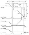
以下、図4および図5を参照しながら、撮像装置I1において画素信号を読み出すためのシーケンスを説明する。撮像装置I1によると、1回目の信号読出しが第1期間T1において為され、2回目の信号読出しが第2期間T2において為されうる。第1期間T1では、画素102の状態を初期化(リセット)した直後の信号(N成分と称する)が読み出されうる。第2期間T2では、当該初期化から所定の時間が経過した後に画素102からの信号(S成分と称する)が読み出されうる。その後、これら2つの信号の差分についてAD変換が為される。ここで、S成分は、画素102において生じる電荷の量、すなわち画素102への入射光の光量にしたがうため、例えば、入射光の光量が多いときはN成分とS成分との差が大きく、光量が少ないときは当該差が小さくなる。なお、画素信号の読み出し方法は、本実施形態で例示する回路構成に限られず、例えば、相関二重サンプリング(CDS)法にしたがう回路構成を採用してもよい。画素アレイ101とADコンバータ201及び202との間にCDS回路を備える場合には、CDS回路の入力部をリセットしたことによる信号がN成分として第1期間T1に読み出されうる。また、CDS回路を介して出力された画素102からの信号がS成分として第2期間T2に読み出されうる。
Hereinafter, a sequence for reading out pixel signals in the imaging apparatus I1 will be described with reference to FIGS. 4 and 5. FIG. According to the imaging apparatus I1, the first signal readout can be performed in the first period T1, and the second signal readout can be performed in the second period T2. In the first period T1, a signal (referred to as an N component) immediately after the state of the
図4は、画素102への入射光の光量が少ない、すなわち輝度レベルが低い場合(低照度時)における撮像装置I1のタイミングチャートを示している。まず、第1期間T1では、N成分の信号についてAD変換を行うイネーブル信号がタイミングジェネレータ118から出力され、1回目の比較が為される。第1期間T1では、ADコンバータ201において、N成分の信号とランプ信号Vref1との比較が為される。当該比較においては、カウンタ207はカウントダウン動作を行う。2つの信号の大小関係が逆転した(例えば、コンパレータ203の出力がLowレベルからHiレベルになった)とき、カウンタ207によるカウントダウンは停止される。ADコンバータ202においては、ADコンバータ201と同様にして、N成分の信号とランプ信号Vref2との比較が為されうる。
FIG. 4 shows a timing chart of the imaging apparatus I1 when the amount of light incident on the
次に、第2期間T2では、S成分の信号についてAD変換を行うイネーブル信号がタイミングジェネレータ118から出力され、2回目の比較が為される。第2期間T2では、ADコンバータ201において、S成分の信号とランプ信号Vref1との比較が為される。当該比較においては、カウンタ207はカウントアップ動作を行う。2つの信号の大小関係が逆転したとき、カウンタ207によるカウントアップは停止される。第1期間T1におけるカウントダウンおよび第2期間T2におけるカウントアップの結果により、カウンタ207の初期値からの変化分が、取得すべきデジタル信号として得られうる。
Next, in the second period T2, an enable signal for performing AD conversion on the S component signal is output from the
また、第2期間T2では、ADコンバータ202においては、ADコンバータ201と同様にして、S成分の信号とランプ信号Vref2との比較が為されうる。前述のとおり、ランプ信号Vref1とランプ信号Vref2とは、例えば、互いに同じ傾きを有しており、ランプ信号Vref2は、ランプ信号Vref1に対してオフセット成分を有する。輝度レベルが低い本ケースにおいては、ADコンバータ202のコンパレータ204の比較結果は第1期間T1の後から反転したまま(ここでは、コンパレータ204の出力がHiレベルのまま)である。すなわち、ADコンバータ202においては、画素アレイからの信号а0は、コンパレータ204による比較が可能な範囲を超えているため、カウンタ208によるカウントアップを省略してもよい。
In the second period T2, the
よって、輝度レベルが低い本ケースにおいては、ラッチ212は、ADコンバータ201のコンパレータ203からの出力であるHiレベル「1」を保持する。セレクタ214は、これに基づいて、デジタル信号d1を選択して出力する。
Therefore, in this case where the luminance level is low, the
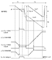
図5は、画素102への入射光の光量が多い、すなわち輝度レベルが高い場合(高照度時)における撮像装置I1のタイミングチャートを、図4と同様にして示している。第1期間T1については、図4と同様であるため説明を省略する。第2期間T2では、輝度レベルが高い本ケースにおいては、S成分が大きいため、ADコンバータ201のコンパレータ203の比較結果は第1期間T1の後から反転しない(ここでは、Lowレベルのまま)。一方で、ADコンバータ202のコンパレータ204の比較結果は第1期間T1の後に反転する(ここでは、LowレベルからHiレベルになる)。よって、輝度レベルが高い本ケースにおいては、ラッチ212はLowレベル「0」を保持し、これに基づいて、セレクタ214はデジタル信号d2を選択して出力する。
FIG. 5 shows a timing chart of the imaging apparatus I1 in the same manner as FIG. 4 when the amount of light incident on the
撮像装置I1の構成によると、ランプ信号Vref1は、例えば、画素アレイ101からの信号а0のダイナミックレンジにおける第1の範囲R1および第2の範囲R2のうちの一方(例えば、範囲R1)に含まれる信号との比較に用いられうる。また、ランプ信号Vref2は、範囲R1および範囲R2のうちの他方(例えば、範囲R2)に含まれる信号との比較に用いられうる。これら2つの参照信号を用いて、画素アレイ101から読み出された1つのアナログ信号(画素信号а0)に対して2つのAD変換を並列に行うことによって、2つのデジタル信号(デジタル信号d1およびデジタル信号d2)が得られる。
According to the configuration of the imaging device I1, the ramp signal Vref1 is included, for example, in one of the first range R1 and the second range R2 (for example, the range R1) in the dynamic range of the signal a0 from the
出力部U1は、2つのデジタル信号のうちの一方を出力し、出力部U2は、出力部U1が2つのデジタル信号のうちのいずれを出力したかを示す情報(情報di)を出力する。撮像装置I1は、出力部U1および出力部U2から出力(デジタル信号)を、例えば、情報diを1ビットのヘッダとして含むデジタル信号として外部モジュールに出力すればよい。すなわち、1ビットの情報がヘッダとして付加されたデジタル信号が撮像装置I1の内部において生成される。よって、撮像装置I1の出力先である外部モジュール(例えば、前述の処理部)において取り扱われるデジタル信号のデータ量が低減され、例えば、2つのデジタル信号についての加算処理などのデータ処理が省略されうる。以上、本実施形態によると、撮像装置I1により得られる信号の信号処理が容易になり、例えば、画像処理の高速化や低電力化に有利である。 The output unit U1 outputs one of the two digital signals, and the output unit U2 outputs information (information di) indicating which of the two digital signals is output by the output unit U1. The imaging apparatus I1 may output the output (digital signal) from the output unit U1 and the output unit U2, for example, as a digital signal including the information di as a 1-bit header to the external module. That is, a digital signal to which 1-bit information is added as a header is generated inside the imaging apparatus I1. Therefore, the data amount of the digital signal handled in the external module (for example, the above-described processing unit) that is the output destination of the imaging device I1 is reduced, and for example, data processing such as addition processing for two digital signals can be omitted. . As described above, according to the present embodiment, signal processing of the signal obtained by the imaging device I1 is facilitated, which is advantageous, for example, in speeding up image processing and reducing power consumption.
上述の実施形態では、ランプ信号Vref1およびランプ信号Vref2のそれぞれは、信号出力部108および信号出力部109のそれぞれから、それぞれ出力される構成を示したが、本発明は、当該構成に限られるものではない。例えば、撮像装置I1aは、図6に示されるように、容量1301および信号出力部108Xを備え、これらの接続関係をスイッチ1302により切り替えることによって、2つのランプ信号を生成してもよい。具体的には、信号出力部108Xは、容量1301の充電を行った後にランプ波形の信号を出力する。撮像装置I1aは、当該信号をランプ信号Vref1として使用し、また、充電によって生じた容量の電圧をランプ信号Vref1に対するオフセット成分とするランプ信号Vref2として使用することができる。
In the above-described embodiment, the ramp signal Vref1 and the ramp signal Vref2 are output from the
また、上述の実施形態では、互いに同じ傾きを有するランプ信号Vref1とランプ信号Vref2とを用いて2つのAD変換を行う構成を述べたが、互いに異なる傾きを有するランプ信号Vref1とランプ信号Vref2とを用いて2つのAD変換を行うこともできる。例えば、範囲R1と範囲R2とが互いに異なるレンジ幅を有し、ランプ信号Vref1とランプ信号Vref2との傾きの比が、範囲R1と範囲R2とのレンジ幅の比にしたがうようにすればよい。また、本発明の趣旨を逸脱しない限り、図7に例示されるように、範囲R1と範囲R2とは重複する範囲を有していてもよい。 In the above-described embodiment, the configuration in which two AD conversions are performed using the ramp signal Vref1 and the ramp signal Vref2 having the same inclination is described. However, the ramp signal Vref1 and the ramp signal Vref2 having different inclinations are described. Two AD conversions can also be performed. For example, the range R1 and the range R2 may have different range widths, and the ratio of the slopes of the ramp signal Vref1 and the ramp signal Vref2 may follow the ratio of the range widths of the range R1 and the range R2. Moreover, unless it deviates from the meaning of this invention, range R1 and range R2 may have the range which overlaps so that it may be illustrated in FIG.
(第2実施形態)
図8乃至10を参照しながら、第2実施形態の撮像装置I2を説明する。本実施形態は、AD変換を行うための構成が第1実施形態と異なる。撮像装置I2は、図8に例示されるように、定電圧源602(第1のユニット)および積分回路601(第2のユニット)を備えうる。定電圧源602は、例えば、画素アレイ101からの信号а0(例えば、正の電圧)とは極性が異なる一定の信号(例えば、負の電圧)を出力すればよい。
(Second Embodiment)
The imaging device I2 of the second embodiment will be described with reference to FIGS. This embodiment is different from the first embodiment in the configuration for performing AD conversion. As illustrated in FIG. 8, the imaging device I2 can include a constant voltage source 602 (first unit) and an integration circuit 601 (second unit). The
積分回路601は、スイッチ603を用いて、画素アレイ101(の列信号線105)および定電圧源602のいずれか一方に接続されうる。積分回路601は、画素アレイ101からの信号а0の積分を行った後に、定電圧源602からの信号の積分を行う。
The
ADコンバータ201は、積分回路601からの出力信号i0と、参照信号Vref1(第1の参照信号)との比較を行うことによってAD変換を行う(第1のアナログデジタル変換)。また、ADコンバータ202は、積分回路601からの出力信号i0と、参照信号Vref1とは異なる参照信号Vref2(第2の参照信号)との比較を行うことによってAD変換を行う(第2のアナログデジタル変換)。本実施形態では、信号出力部108および109からの参照信号Vref1およびVref2には、ランプ波形の信号ではなく、矩形の波形の信号が用いられうる。
The
当該矩形の波形は、参照信号Vref1と参照信号Vref2で互いに異なる値を有しており、参照信号Vref2は、参照信号Vref1に対してオフセット成分を有する。参照信号Vref1は、積分回路601からの出力信号i0のダイナミックレンジにおける範囲R1および範囲R2のうちの一方(例えば、範囲R1)に含まれる信号との比較に用いられうる。参照信号Vref2は、範囲R1および範囲R2のうちの他方(例えば、範囲R2)に含まれる信号との比較に用いられうる。
The rectangular waveform has different values for the reference signal Vref1 and the reference signal Vref2, and the reference signal Vref2 has an offset component with respect to the reference signal Vref1. The reference signal Vref1 can be used for comparison with a signal included in one of the ranges R1 and R2 (eg, range R1) in the dynamic range of the output signal i0 from the
以下、第1実施形態と同様にして、図9および図10を参照しながら、撮像装置I2における画素アレイ101からの信号を読み出すためのシーケンスを説明する。
Hereinafter, as in the first embodiment, a sequence for reading signals from the
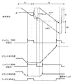
図9は、輝度レベルが低い場合における撮像装置I2のタイミングチャートを示している。第1実施形態と同様に、第1期間T1では1回目の比較が為される。本実施形態では、具体的には、第1期間T1のうちの期間t11において、積分回路601はスイッチ603によって列信号線105に接続され、画素アレイ101のN成分の信号が積分回路601に入力されて積分回路601の出力i0が上昇する。その後の期間t12において、積分回路601はスイッチ603によって定電圧源602に接続され、定電圧源602からの信号は画素アレイ101のN成分の信号とは極性が逆であるため、積分回路601の出力i0が降下する。ADコンバータ201において、積分回路601の出力i0と、参照信号Vref1との比較が為される。積分回路601の出力i0と、参照信号Vref1との大小関係が逆転した(例えば、コンパレータ203の出力がLowレベルからHiレベルになった)とき、カウンタ207によるカウントダウンは停止される。ADコンバータ202においてもADコンバータ201と同様の動作が為されうる。
FIG. 9 shows a timing chart of the imaging apparatus I2 when the luminance level is low. Similar to the first embodiment, the first comparison is performed in the first period T1. In the present embodiment, specifically, in the period t11 of the first period T1, the
第2期間T2では2回目の比較が為される。具体的には、第2期間T2のうちの期間t21においては、積分回路601は、スイッチ603により列信号線105に接続され、画素アレイ101のS成分の信号が積分回路601に入力され、積分回路601の出力i0は上昇する。その後の期間t22においては、積分回路601は、スイッチ603により定電圧源602に接続され、積分回路601の出力i0は降下する。ADコンバータ201においては、積分回路601の出力i0と、参照信号Vref1との大小関係が逆転し、コンパレータ203の出力がLowレベルからHiレベルになったとき、カウンタ207によるカウントダウンは停止される。
The second comparison is performed in the second period T2. Specifically, in the period t21 of the second period T2, the integrating
また、第2期間T2では、ADコンバータ202においては、ADコンバータ201と同様にして、積分回路601の出力i0と、参照信号Vref2との比較が為されうる。ここで、前述のとおり、参照信号Vref2は、参照信号Vref1に対してオフセット成分を有する。輝度レベルが低い本ケースにおいては、ADコンバータ202のコンパレータ204の比較結果は第1期間T1の後から反転したまま(ここでは、コンパレータ204の出力がHiレベルのまま)であり、カウンタ208はカウントアップを行わなくてもよい。
In the second period T2, the
よって、輝度レベルが低い本ケースにおいては、第1実施形態と同様にして、ラッチ212はHiレベル「1」を保持し、これに基づいて、セレクタ214はデジタル信号d1を選択して出力する。
Therefore, in this case where the luminance level is low, the
図10は、輝度レベルが高い場合における撮像装置I2のタイミングチャートを示している。第1期間T1については、図9と同様であるため説明を省略する。第2期間T2では、輝度レベルが高い本ケースにおいては、S成分が大きいため、ADコンバータ201のコンパレータ203の比較結果は第1期間T1の後から反転しない(ここでは、Lowレベルのまま)。一方で、ADコンバータ202のコンパレータ204の比較結果は第1期間T1の後に反転する(ここでは、LowレベルからHiレベルになる)。よって、輝度レベルが高い本ケースにおいては、ラッチ212はLowレベル「0」を保持し、これに基づいて、セレクタ214はデジタル信号d2を選択して出力する。
FIG. 10 shows a timing chart of the imaging apparatus I2 when the luminance level is high. The first period T1 is the same as that in FIG. In the second period T2, in this case where the luminance level is high, since the S component is large, the comparison result of the
以上、本実施形態では、AD変換を行うための構成が第1実施形態と異なる構成について述べたが、本実施形態の構成によっても、第1実施形態と同様の効果が得られる。 As described above, in the present embodiment, the configuration for performing AD conversion is different from that of the first embodiment. However, the same effect as that of the first embodiment can be obtained by the configuration of the present embodiment.
(第3実施形態)
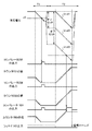
図11乃至13を参照しながら、第3実施形態の撮像装置I3を説明する。本実施形態は、図11に示されるように、AD変換を行うための構成が第1実施形態および第2実施形態と異なる。撮像装置I3においては、ADコンバータ201は、レジスタ901(第1のレジスタ)、DAコンバータ903(第1のDAコンバータ)、およびコンパレータ203(第1のコンパレータ)を含みうる。DAコンバータ903は、参照信号Vref1を基準電位として、レジスタ901の値をアナログ信号a1(第1のアナログ信号)に変換する。コンパレータ203は、画素アレイ101からの信号a0と、アナログ信号a1との比較を行う。
(Third embodiment)
The imaging device I3 according to the third embodiment will be described with reference to FIGS. As shown in FIG. 11, the present embodiment is different from the first and second embodiments in the configuration for performing AD conversion. In the imaging device I3, the
ADコンバータ202は、ADコンバータ201と同様にして、レジスタ902(第2のレジスタ)、DAコンバータ904(第2のDAコンバータ)、およびコンパレータ204(第2のコンパレータ)を含みうる。DAコンバータ904は、参照信号Vref2を基準電位として、レジスタ902の値をアナログ信号a2(第2のアナログ信号)に変換する。コンパレータ204は、画素アレイ101からの信号a0と、アナログ信号a2との比較を行う。
Similarly to the
アナログ信号a2は、アナログ信号a1に対してオフセット成分を有している。アナログ信号a1は、画素アレイ101からの信号a0のダイナミックレンジにおける範囲R1および範囲R2のうちの一方(例えば、範囲R1)に含まれる信号との比較に用いられうる。アナログ信号a2は、範囲R1および範囲R2のうちの他方(例えば、範囲R2)に含まれる信号との比較に用いられうる。
The analog signal a2 has an offset component with respect to the analog signal a1. The analog signal a1 can be used for comparison with a signal included in one of the ranges R1 and R2 (for example, the range R1) in the dynamic range of the signal a0 from the
以下、第1ないし第2実施形態と同様にして、図12および図13を参照しながら、撮像装置I3における画素アレイ101からの信号a0を読み出すためのシーケンスを説明する。
The sequence for reading the signal a0 from the
図12は、輝度レベルが低い場合における撮像装置I3のタイミングチャートを示している。第1期間T1では1回目の比較が為される。具体的には、第1期間T1では、ADコンバータ201においては、レジスタ901の値を順に変化させながら、画素アレイ101からの信号a0とアナログ信号a1との比較が為される。第1期間T1のうちの期間t11では、コンパレータ203は、レジスタ901が「4」(2進数で0100)に設定された状態におけるDAコンバータ903の出力、すなわちアナログ信号a1と、信号a0とを比較する。その結果、コンパレータ203の出力はLowレベルからHiレベルになる。
FIG. 12 shows a timing chart of the imaging device I3 when the luminance level is low. In the first period T1, the first comparison is made. Specifically, in the first period T1, the
その後の期間t12では、レジスタ901が「2」(2進数で0010)に設定され、コンパレータ203はアナログ信号a1と信号a0とを比較する。アナログ信号a1と信号a0との大小関係は逆転しないため、コンパレータ203の出力はHiレベルのままである。さらに、その後の期間t13では、レジスタ901が「1」(2進数で0001)に設定され、コンパレータ203はアナログ信号a1と信号a0とを比較する。アナログ信号a1と信号a0との大小関係は逆転し、コンパレータ203の出力はHiレベルからLowレベルになる。このようにして、レジスタ901の値「1」(2進数で0001)が1回目の比較の結果として得られ、例えば、レジスタ(不図示)に保持されうる。ADコンバータ202においてもADコンバータ201と同様の動作が為されうる。
In the subsequent period t12, the
第2期間T2では2回目の比較が為される。第2期間T2のうちの期間t21では、レジスタ901が「8」(2進数で1000)に設定され、コンパレータ203は、アナログ信号a1と信号a0とを比較する。その結果、コンパレータ203の出力はLowレベルからHiレベルになる。その後の期間t22では、レジスタ901が「4」(2進数で0100)に設定され、コンパレータ203の出力はHiレベルからLowレベルになる。次に、期間t23では、レジスタ901が「6」(2進数で0110)に設定され、コンパレータ203の出力はLowレベルからHiレベルになる。さらに、期間t24では、レジスタ901が「5」(2進数で0101)に設定され、コンパレータ203の出力はHiレベルのままである。レジスタ901の4ビットの値のそれぞれは、4入力AND回路907の各入力端子にそれぞれ入力される。輝度レベルが低い本ケースにおいては、レジスタ901の値は「0101」であるので、ラッチ212には「0」が入力される。
The second comparison is performed in the second period T2. In the period t21 of the second period T2, the
なお、第2期間T2では、ADコンバータ202においては、ADコンバータ201と同様にして、アナログ信号a2と信号a0との比較が為されうる。ここで、前述のとおり、アナログ信号a2は、アナログ信号a1に対してオフセット成分を有する。輝度レベルが低い本ケースにおいては、コンパレータ204の出力もHiレベルである。
In the second period T2, the
このようにして、レジスタ901の値「5」(2進数で0101)が2回目の比較の結果として得られる。輝度レベルが低い本ケースにおいては、ラッチ212は、4入力AND回路907からの出力である「0」を保持する。よって、これに基づいて、セレクタ214は、ADコンバータ201における1回目の比較と2回目の比較との差分を、取得すべきデジタル信号d1を選択して出力する。
In this way, the value “5” (binary 0101) in the
図13は、輝度レベルが高い場合における撮像装置I3のタイミングチャートを示している。第1期間T1については、図12と同様であるため説明を省略する。一方、第2期間T2では、輝度レベルが高い本ケースにおいては、アナログ信号a1と信号a0との比較が前述と同様の手順で為されるが、S成分が大きいため、コンパレータ203の比較結果は第1期間T1の後から反転しない(Lowレベルのまま)。その結果、レジスタ901の値は、「F」(2進数で1111)まで変化する。輝度レベルが高い本ケースにおいては、レジスタ901の値は「1111」であるので、ラッチ212には「1」が入力される。
FIG. 13 shows a timing chart of the imaging apparatus I3 when the luminance level is high. The first period T1 is the same as that in FIG. On the other hand, in the second period T2, in this case where the luminance level is high, the comparison between the analog signal a1 and the signal a0 is performed in the same procedure as described above, but since the S component is large, the comparison result of the
一方で、ADコンバータ202のコンパレータ204の比較結果は第1期間T1の後に反転し、アナログ信号a2と信号a0との比較が、前述と同様の手順で為される。ここでは、レジスタ902の値「3」(2進数で0011)が2回目の比較の結果として得られる。輝度レベルが高い本ケースにおいては、ラッチ212は、4入力AND回路907からの出力である「1」を保持する。よって、これに基づいて、セレクタ214は、ADコンバータ202における1回目の比較と2回目の比較との差分を、取得すべきデジタル信号d2を選択して出力する。
On the other hand, the comparison result of the
以上、本実施形態では、AD変換を行うための構成が第1ないし第2実施形態と異なる構成について述べたが、本実施形態の構成によっても、第1ないし第2実施形態と同様の効果が得られる。 As described above, in the present embodiment, the configuration for performing AD conversion is different from that of the first or second embodiment. However, the configuration of this embodiment also has the same effect as that of the first or second embodiment. can get.
(第4実施形態)
図14乃至16を参照しながら、第4実施形態の撮像装置I4を説明する。以上の第1ないし第3実施形態では、画素アレイ101における複数の列のそれぞれに2つのADコンバータ(ADコンバータ201および202)が設けられた構成を述べたが、本実施形態では、動作モードに応じて構成を変更する。
(Fourth embodiment)
The imaging device I4 according to the fourth embodiment will be described with reference to FIGS. In the above first to third embodiments, the configuration in which two AD converters (
撮像装置I4は、画素アレイ101の各列に対応して1つのADコンバータが配されうる。例えば、図14に示されるように、ADコンバータ201は第L1列目(L1は奇数の整数)に対応して配されており、ADコンバータ202は第L2列目(L2は偶数の整数)に対応して配されている。換言すると、第L1列は、第1群(奇数の列)のうちの1列であり、第L2列は、第2群(偶数の列)のうちの1列である。
In the imaging device I4, one AD converter can be arranged corresponding to each column of the
撮像装置I4は、動作モードとして、例えば第1モードおよび第2モードを含みうる。第1モードでは、画素アレイ101の複数の列のそれぞれから信号が読み出され、いわゆる全読出しが為される。第2モードでは、画素アレイ101の複数の列のうち、例えば、第1群(ここでは、奇数の列)の各画素から信号が読み出され、いわゆる間引き読出しが為される。撮像装置I4は、例えば、スイッチ部1401および1402を備え、動作モードに応じて、ADコンバータ201およびADコンバータ202の接続関係を切り替える。
The imaging device I4 can include, for example, a first mode and a second mode as operation modes. In the first mode, signals are read from each of the plurality of columns of the
例えば、第1モードでは、スイッチ部1401および1402は、ADコンバータ201が第L1列目からの信号についてAD変換を行い、ADコンバータ202が第L2列目からの信号についてAD変換を行うように、ADコンバータ201および202の接続関係を切り替える。一方、第2モードでは、スイッチ部1401および1402は、ADコンバータ201およびADコンバータ202のそれぞれが第L1列目からの信号についてAD変換を並列に行うように当該接続関係を切り替える。
For example, in the first mode, the
以上、本実施形態によると、撮像装置I4は、第1モードにおいては、各列に設けられたADコンバータが各列の画素信号の読出しにそれぞれ対応するように動作させる。一方、撮像装置I4は、第2モードにおいては、画素信号の読出しを省略する各列に設けられたADコンバータを、画素信号の読出しを行う各列に設けられたADコンバータと並列に動作させる。よって、撮像装置I4は、第2モードにおいて第1ないし第3実施形態と同様の効果を達成する。また、ここでは、第2モードにおいては、画素信号が、奇数の列の各画素から読み出される構成を述べたが、偶数の列の各画素から読み出される構成にしてもよい。 As described above, according to the present embodiment, in the first mode, the imaging device I4 operates the AD converters provided in each column so as to correspond to the readout of the pixel signals in each column. On the other hand, in the second mode, the imaging device I4 operates the AD converters provided in the respective columns from which pixel signals are not read out in parallel with the AD converters provided in the respective columns from which the pixel signals are read out. Therefore, the imaging device I4 achieves the same effect as in the first to third embodiments in the second mode. Further, here, in the second mode, the configuration in which the pixel signal is read from each pixel in the odd-numbered column has been described. However, the pixel signal may be read from each pixel in the even-numbered column.
また、第2モードによる間引き読出しは、画素アレイ101から3列ごと間隔で信号を読み出すように構成してもよく、例えば、図15に例示される撮像装置I4aのように構成してもよい。撮像装置I4aによると、第2モードにおいては、3の倍数の列の各画素から画素信号が読み出される。ここでは、画素アレイ101のうちの3列(第L1列目、第L2列目および第L3列目)を例示して述べる。ここで、mを整数として、ADコンバータ201は第L1列目(L1=3m−2)に対応して配されている。ADコンバータ202は第L2列目(L2=3m−1)に対応して配されている。ADコンバータ203は第L3列目(L3=3m)に対応して配されている。
Further, the thinning-out readout in the second mode may be configured to read out signals from the
例えば、第1モードでは、スイッチ部1401および1402は、3つのADコンバータのそれぞれが、画素アレイ101の3列からの信号のそれぞれについて、それぞれAD変換を行うように、3つのADコンバータの接続関係を切り替える。より具体的には、スイッチ部1401および1402は、ADコンバータ201が第L1列目からの信号についてAD変換を行う。ADコンバータ202が第L2列目からの信号についてAD変換を行う。また、ADコンバータ203が第L3列目からの信号についてAD変換を行うよう。
For example, in the first mode, the
一方、第2モードでは、スイッチ部1401および1402は、ADコンバータ201ないし203のそれぞれが第L1列目からの信号についてAD変換を並列に行うように当該接続関係を切り替える。図16は、輝度レベルが高い場合における撮像装置I4aのタイミングチャートを前述の各実施形態と同様にして例示している。
On the other hand, in the second mode, the
以上の4つの実施形態を述べたが、本発明はこれらに限られるものではなく、目的、状態、用途及び機能その他の仕様に応じて、適宜、変更が可能であり、他の実施形態によっても為されうる。 Although the above-described four embodiments have been described, the present invention is not limited to these, and can be appropriately changed according to the purpose, state, application, function, and other specifications. Can be done.
(撮像システム)
以上の実施形態は、カメラ等に代表される撮像システムに含まれる撮像装置について述べた。撮像システムの概念には、撮影を主目的とする装置のみならず、撮影機能を補助的に備える装置(例えば、パーソナルコンピュータ、携帯端末)も含まれる。撮像システムは、上記の実施形態として例示された本発明に係る撮像装置と、この撮像装置から出力される信号を処理する処理部とを含みうる。この処理部は、例えば、A/D変換器、および、このA/D変換器から出力されるデジタルデータを処理するプロセッサを含みうる。
(Imaging system)
The above embodiment described the imaging device included in the imaging system represented by a camera or the like. The concept of the imaging system includes not only a device mainly for photographing, but also a device (for example, a personal computer or a portable terminal) that is supplementarily provided with a photographing function. The imaging system can include an imaging apparatus according to the present invention exemplified as the above-described embodiment, and a processing unit that processes a signal output from the imaging apparatus. The processing unit may include, for example, an A / D converter and a processor that processes digital data output from the A / D converter.
Claims (17)
前記第1の信号に対して、第1の電位から第2の電位まで変化する第1の参照信号を用いて第1のアナログデジタル変換を行う第1のADコンバータと、
前記第1の信号に対して、前記第1の電位とは異なる第3の電位から前記第2の電位とは異なる第4の電位まで変化する第2の参照信号を用いて第2のアナログデジタル変換を行う第2のADコンバータと、
前記第1のADコンバータにおける前記第1のアナログデジタル変換により得られた第1のデジタル信号、および、前記第2のADコンバータにおける前記第2のアナログデジタル変換により得られた第2のデジタル信号のうちの一方を出力する第1の出力部と、
前記第1の出力部の出力が前記第1のデジタル信号および前記第2のデジタル信号のいずれであるかを示す情報を出力する第2の出力部と、を備える、
ことを特徴とする撮像装置。 A plurality of pixels each provided with a photoelectric conversion unit are arranged so as to form a plurality of rows and a plurality of columns, and a pixel array that outputs a signal based on charges generated in the photoelectric conversion unit as a first signal;
With respect to the first signal, a first first AD converter that performs a first analog-to-digital conversion using a first reference signal that changes from the potential to the second potential,
With respect to the first signal , a second analog-digital signal is output using a second reference signal that changes from a third potential different from the first potential to a fourth potential different from the second potential. A second AD converter for performing the conversion;
A first digital signal obtained by the first analog-digital conversion in the first AD converter, and a second digital signal obtained by the second analog-digital conversion in the second AD converter. A first output unit for outputting one of them;
A second output unit that outputs information indicating whether the output of the first output unit is the first digital signal or the second digital signal;
An imaging apparatus characterized by that.
ことを特徴とする請求項1に記載の撮像装置。 The imaging apparatus according to claim 1, wherein the second AD converter performs the second analog-digital conversion in parallel with the first analog-digital conversion performed by the first AD converter.
前記第2の参照信号は、前記第1の参照信号と同じ傾きを有し、前記第1の参照信号に対してオフセット成分を有する、
ことを特徴とする請求項2に記載の撮像装置。 The first reference signal and the second reference signal are both ramp signals,
The second reference signal has the same slope as the first reference signal and has an offset component with respect to the first reference signal.
The imaging apparatus according to claim 2.
前記信号出力部は、前記容量の充電を行った後に前記ランプ信号を出力することによって、当該ランプ信号を前記第1の参照信号として出力し、前記充電によって生じた前記容量の電圧を前記第1の参照信号に対する前記オフセット成分とする前記第2の参照信号として出力する、
ことを特徴とする請求項3に記載の撮像装置。 A signal output unit and a capacitor;
The signal output unit outputs the ramp signal as the first reference signal by outputting the ramp signal after charging the capacitor, and outputs the voltage of the capacitor generated by the charging to the first. Output as the second reference signal as the offset component with respect to the reference signal of
The imaging apparatus according to claim 3.
前記画素アレイからの信号のダイナミックレンジは、互いに異なるレンジ幅である第1の範囲および第2の範囲を有しており、
前記第1の参照信号は、前記第1の範囲および前記第2の範囲の一方に含まれる信号のアナログデジタル変換に用いられ、
前記第2の参照信号は、前記第1の範囲および前記第2の範囲の他方に含まれる信号のアナログデジタル変換に用いられ、
前記第1の参照信号と前記第2の参照信号との傾きの比は、前記第1の範囲と前記第2の範囲とのレンジ幅の比にしたがう、
ことを特徴とする請求項1乃至4のいずれか1項に記載の撮像装置。 The first reference signal and the second reference signal are both ramp signals,
The dynamic range of the signal from the pixel array has a first range and a second range having different range widths,
The first reference signal is used for analog-to-digital conversion of a signal included in one of the first range and the second range,
The second reference signal is used for analog-digital conversion of signals included in the other of the first range and the second range,
The ratio of the slope between the first reference signal and the second reference signal is in accordance with the ratio of the range width between the first range and the second range.
The image pickup apparatus according to claim 1, wherein the image pickup apparatus is an image pickup apparatus.
前記第2のADコンバータは、カウントアップおよびカウントダウンの少なくとも一方を行って、前記画素アレイからの前記信号と前記第2の参照信号との大小関係が逆転するまでの時間を計測するカウンタを含む、
ことを特徴とする請求項1乃至5のいずれか1項に記載の撮像装置。 The first AD converter includes a counter that performs at least one of count-up and count-down and measures a time until the magnitude relationship between the signal from the pixel array and the first reference signal is reversed,
The second AD converter includes a counter that performs at least one of count-up and count-down and measures a time until the magnitude relationship between the signal from the pixel array and the second reference signal is reversed.
The imaging apparatus according to any one of claims 1 to 5, wherein
前記第1の信号とは極性が異なる一定の信号を出力する第1のユニットと、
前記第1のユニットまたは前記画素アレイに接続され、前記画素アレイからの前記第1の信号の積分を行った後に前記第1のユニットからの信号の積分を行う第2のユニットと、
前記第2のユニットからの出力信号と第1の参照信号との比較を行うことによって第1のアナログデジタル変換を行う第1のADコンバータと、
前記第1のADコンバータによる前記第1のアナログデジタル変換と並列に、前記第2のユニットからの前記出力信号と、前記第1の参照信号とは異なる第2の参照信号との比較を行うことによって第2のアナログデジタル変換を行う第2のADコンバータと、
前記第1のADコンバータにおける前記第1のアナログデジタル変換により得られた第1のデジタル信号、および前記第2のADコンバータにおける前記第2のアナログデジタル変換により得られた第2のデジタル信号のうちの一方を出力する第1の出力部と、
前記第1の出力部の出力が前記第1のデジタル信号および前記第2のデジタル信号のいずれであるかを示す情報を出力する第2の出力部と、を備え、
前記第1の参照信号は、前記第2のユニットからの出力信号のダイナミックレンジにおける第1の範囲および第2の範囲のうちの一方に含まれる信号との比較に用いられ、前記第2の参照信号は、前記第1の範囲および前記第2の範囲のうちの他方に含まれる信号との比較に用いられる、
ことを特徴とする撮像装置。 A plurality of pixels each provided with a photoelectric conversion unit are arranged so as to form a plurality of rows and a plurality of columns, and a pixel array that outputs a signal based on charges generated in the photoelectric conversion unit as a first signal;
A first unit for outputting a constant signal having a polarity different from that of the first signal;
A second unit connected to the first unit or the pixel array and integrating the signal from the first unit after integrating the first signal from the pixel array;
A first AD converter that performs a first analog-to-digital conversion by comparing an output signal from the second unit with a first reference signal;
In parallel with the first analog-to-digital conversion by the first AD converter, the output signal from the second unit is compared with a second reference signal different from the first reference signal. A second AD converter for performing a second analog-digital conversion by:
Of the first digital signal obtained by the first analog-digital conversion in the first AD converter and the second digital signal obtained by the second analog-digital conversion in the second AD converter A first output unit that outputs one of the following:
A second output unit that outputs information indicating whether the output of the first output unit is the first digital signal or the second digital signal;
The first reference signal is used for comparison with a signal included in one of a first range and a second range in a dynamic range of an output signal from the second unit, and the second reference The signal is used for comparison with a signal included in the other of the first range and the second range.
Imaging device you wherein a.
前記第2のADコンバータは、第2のレジスタ、前記第2のレジスタの値を第2の参照信号に基づいて第2のアナログ信号に変換する第2のDAコンバータ、および前記画素アレイからの前記信号と前記第2のアナログ信号とを比較する第2のコンパレータを含み、
前記第1のアナログ信号は、前記画素アレイからの信号のダイナミックレンジにおける第1の範囲および第2の範囲のうちの一方に含まれる信号との比較に用いられ、前記第2のアナログ信号は、前記第1の範囲および前記第2の範囲のうちの他方に含まれる信号との比較に用いられる、
ことを特徴とする請求項1に記載の撮像装置。 The first AD converter includes a first register, a first DA converter that converts a value of the first register into a first analog signal based on a first reference signal, and the pixel array A first comparator for comparing a signal with the first analog signal;
The second AD converter includes a second register, a second DA converter that converts a value of the second register into a second analog signal based on a second reference signal, and the pixel array A second comparator for comparing a signal and the second analog signal;
The first analog signal is used for comparison with a signal included in one of a first range and a second range in a dynamic range of a signal from the pixel array, and the second analog signal is: Used for comparison with signals included in the other of the first range and the second range;
The imaging apparatus according to claim 1.
ことを特徴とする請求項1乃至8のいずれか1項に記載の撮像装置。 A digital signal that includes one of the first digital signal and the second digital signal from the first output unit and the information from the second output unit as a 1-bit header. Output,
The image pickup apparatus according to claim 1, wherein the image pickup apparatus is an image pickup apparatus.
ことを特徴とする請求項1乃至9のいずれか1項に記載の撮像装置。 The first AD converter is arranged corresponding to each of the plurality of columns of the plurality of pixels, and the second AD converter is arranged corresponding to each of the plurality of columns. ing,
The image pickup apparatus according to claim 1, wherein the image pickup apparatus is an image pickup apparatus.
前記撮像装置は、前記画素アレイの前記複数の列のそれぞれから信号を読み出す第1モードと、当該複数の列のうちの第1群のそれぞれから信号を読み出す第2モードとを動作モードとして含み、
前記スイッチ部により、前記第1モードにおいては、前記第1のADコンバータが前記第1群のうちの1列に対応し、前記第2のADコンバータが前記第1群とは異なる第2群のうちの1列に対応し、前記第2モードにおいては、前記第1のADコンバータおよび前記第2のADコンバータが前記第1群のうちの1列に対応する、
ことを特徴とする請求項1乃至9のいずれか1項に記載の撮像装置。 It further has a switch part,
The imaging device includes, as operation modes, a first mode for reading signals from each of the plurality of columns of the pixel array and a second mode for reading signals from each of the first group of the plurality of columns,
By the switch unit, in the first mode, the first AD converter corresponds to one column of the first group, and the second AD converter is different from the first group in the second group. Corresponding to one of the columns, and in the second mode, the first AD converter and the second AD converter correspond to one column of the first group,
The image pickup apparatus according to claim 1, wherein the image pickup apparatus is an image pickup apparatus.
ことを特徴とする請求項1乃至11のいずれか1項に記載の撮像装置。 The first output unit includes a selector that selects one of the first digital signal and the second digital signal based on an output of the first AD converter.
The image pickup apparatus according to claim 1, wherein the image pickup apparatus is an image pickup apparatus.
ことを特徴とする請求項12に記載の撮像装置。 The first output unit further includes a latch that holds the output from the first AD converter.
The imaging apparatus according to claim 12.
前記画素アレイからの信号であって第1の範囲に含まれる値を有する信号に対して第1のアナログデジタル変換を行う第1のADコンバータと、 A first AD converter that performs a first analog-digital conversion on a signal from the pixel array that has a value included in a first range;
前記第1のADコンバータによる前記第1のアナログデジタル変換と並列に、前記画素アレイからの信号であって前記第1の範囲とは異なる第2の範囲に含まれる値を有する信号に対して第2のアナログデジタル変換を行う第2のADコンバータと、 In parallel with the first analog-to-digital conversion by the first AD converter, a signal having a value included in a second range different from the first range is a signal from the pixel array. A second AD converter that performs analog-digital conversion of 2;
前記第1のADコンバータにおける前記第1のアナログデジタル変換により得られた第1のデジタル信号、および、前記第2のADコンバータにおける前記第2のアナログデジタル変換により得られた第2のデジタル信号のうちの一方を出力する第1の出力部と、 A first digital signal obtained by the first analog-digital conversion in the first AD converter, and a second digital signal obtained by the second analog-digital conversion in the second AD converter. A first output unit for outputting one of them;
前記第1の出力部の出力が前記第1のデジタル信号および前記第2のデジタル信号のいずれであるかを示す情報を出力する第2の出力部と、を備える、 A second output unit that outputs information indicating whether the output of the first output unit is the first digital signal or the second digital signal;
ことを特徴とする撮像装置。 An imaging apparatus characterized by that.
前記撮像装置から出力される信号を処理する処理部と、
を備えることを特徴とする撮像システム。 The imaging device according to any one of claims 1 to 14 ,
A processing unit for processing a signal output from the imaging device;
An imaging system comprising:
前記第1の信号に対して、第1の電位から第2の電位まで変化する第1の参照信号を用いて第1のアナログデジタル変換を行う第1の変換工程と、
前記第1の信号に対して、前記第1の電位とは異なる第3の電位から前記第2の電位とは異なる第4の電位まで変化する第2の参照信号を用いて第2のアナログデジタル変換を行う第2の変換工程と、
前記第1の変換工程により得られた第1のデジタル信号および前記第2の変換工程により得られた第2のデジタル信号のうちの一方を出力する第1の出力工程と、
前記第1の出力工程での出力が前記第1のデジタル信号および前記第2のデジタル信号のいずれであるかを示す情報を出力する第2の出力工程と、を含む、
ことを特徴とする撮像装置の駆動方法。 Imaging including a pixel array in which a plurality of pixels each including a photoelectric conversion unit are arranged to form a plurality of rows and a plurality of columns, and a signal based on charges generated in the photoelectric conversion unit is output as a first signal A method for driving an apparatus, comprising:
With respect to the first signal, a first conversion step of performing a first analog-to-digital conversion using a first reference signal that changes from a first potential to a second potential,
With respect to the first signal , a second analog-digital signal is output using a second reference signal that changes from a third potential different from the first potential to a fourth potential different from the second potential. A second conversion step for performing the conversion;
A first output step of outputting one of the first digital signal obtained by the first conversion step and the second digital signal obtained by the second conversion step;
A second output step of outputting information indicating whether the output in the first output step is the first digital signal or the second digital signal.
A driving method for an imaging apparatus.
前記画素アレイからの信号であって第1の範囲に含まれる値を有する信号に対して第1のアナログデジタル変換を行う第1の変換工程と、 A first conversion step of performing a first analog-digital conversion on a signal from the pixel array and having a value included in a first range;
前記第1の変換工程と並列に、前記画素アレイからの信号であって前記第1の範囲とは異なる第2の範囲に含まれる値を有する信号に対して第2のアナログデジタル変換を行う第2の変換工程と、 In parallel with the first conversion step, second analog-to-digital conversion is performed on a signal from the pixel array having a value included in a second range different from the first range. Two conversion steps;
前記第1の変換工程により得られた第1のデジタル信号および前記第2の変換工程により得られた第2のデジタル信号のうちの一方を出力する第1の出力工程と、 A first output step of outputting one of the first digital signal obtained by the first conversion step and the second digital signal obtained by the second conversion step;
前記第1の出力工程での出力が前記第1のデジタル信号および前記第2のデジタル信号のいずれであるかを示す情報を出力する第2の出力工程と、を含む、 A second output step of outputting information indicating whether the output in the first output step is the first digital signal or the second digital signal.
ことを特徴とする撮像装置の駆動方法。 A driving method for an imaging apparatus.
Priority Applications (3)
| Application Number | Priority Date | Filing Date | Title |
|---|---|---|---|
| JP2013012437A JP6097574B2 (en) | 2013-01-25 | 2013-01-25 | Imaging apparatus, driving method thereof, and imaging system |
| US14/146,037 US20140209784A1 (en) | 2013-01-25 | 2014-01-02 | Image sensing apparatus, driving method therefor, and image sensing system |
| CN201410033768.9A CN103973995B (en) | 2013-01-25 | 2014-01-24 | image sensing apparatus and its driving method |
Applications Claiming Priority (1)
| Application Number | Priority Date | Filing Date | Title |
|---|---|---|---|
| JP2013012437A JP6097574B2 (en) | 2013-01-25 | 2013-01-25 | Imaging apparatus, driving method thereof, and imaging system |
Publications (3)
| Publication Number | Publication Date |
|---|---|
| JP2014146849A JP2014146849A (en) | 2014-08-14 |
| JP2014146849A5 JP2014146849A5 (en) | 2016-03-10 |
| JP6097574B2 true JP6097574B2 (en) | 2017-03-15 |
Family
ID=51221891
Family Applications (1)
| Application Number | Title | Priority Date | Filing Date |
|---|---|---|---|
| JP2013012437A Active JP6097574B2 (en) | 2013-01-25 | 2013-01-25 | Imaging apparatus, driving method thereof, and imaging system |
Country Status (3)
| Country | Link |
|---|---|
| US (1) | US20140209784A1 (en) |
| JP (1) | JP6097574B2 (en) |
| CN (1) | CN103973995B (en) |
Families Citing this family (15)
| Publication number | Priority date | Publication date | Assignee | Title |
|---|---|---|---|---|
| JP5953074B2 (en) * | 2012-03-08 | 2016-07-13 | オリンパス株式会社 | Imaging device |
| EP3103255B1 (en) * | 2014-02-07 | 2021-07-07 | Rambus Inc. | Feedthrough-compensated image sensor |
| TWI672952B (en) * | 2014-03-06 | 2019-09-21 | 日商新力股份有限公司 | Image pickup device, control method, and image pickup apparatus |
| JP2016181736A (en) * | 2015-03-23 | 2016-10-13 | キヤノン株式会社 | Imaging device, method of driving the same, and imaging system |
| JP6639271B2 (en) * | 2015-07-16 | 2020-02-05 | キヤノン株式会社 | Imaging device, imaging system |
| WO2017076748A1 (en) * | 2015-11-06 | 2017-05-11 | Cmosis Bvba | Analog-to-digital conversion and method of analog-to-digital conversion |
| US10348323B2 (en) * | 2015-11-06 | 2019-07-09 | Ams Sensors Belgium Bvba | Analog-to-digital conversion and method of analog-to-digital conversion |
| US10015429B2 (en) * | 2015-12-30 | 2018-07-03 | Omnivision Technologies, Inc. | Method and system for reducing noise in an image sensor using a parallel multi-ramps merged comparator analog-to-digital converter |
| JP6731731B2 (en) * | 2016-01-08 | 2020-07-29 | ブリルニクス インク | Solid-state imaging device, driving method thereof, and electronic device |
| US9955099B2 (en) * | 2016-06-21 | 2018-04-24 | Hand Held Products, Inc. | Minimum height CMOS image sensor |
| JP6987603B2 (en) * | 2017-10-26 | 2022-01-05 | ブリルニクス シンガポール プライベート リミテッド | Solid-state image sensor, solid-state image sensor driving method, and electronic equipment |
| KR102523174B1 (en) * | 2017-11-09 | 2023-04-18 | 주식회사 엘엑스세미콘 | Driver for display devie |
| JP6766095B2 (en) | 2018-06-08 | 2020-10-07 | キヤノン株式会社 | Semiconductor substrates for imaging devices, imaging systems, mobiles, and stacks |
| JP7455573B2 (en) | 2019-12-24 | 2024-03-26 | キヤノン株式会社 | Signal processing devices, photoelectric conversion devices, photoelectric conversion systems, imaging devices, and mobile objects |
| WO2023149417A1 (en) * | 2022-02-07 | 2023-08-10 | ソニーセミコンダクタソリューションズ株式会社 | Imaging device |
Family Cites Families (17)
| Publication number | Priority date | Publication date | Assignee | Title |
|---|---|---|---|---|
| US7129883B2 (en) * | 2004-02-23 | 2006-10-31 | Sony Corporation | Method and apparatus for AD conversion, semiconductor device for detecting distribution of physical quantity, and electronic apparatus |
| DE602005013469D1 (en) * | 2004-11-08 | 2009-05-07 | Sony Corp | A method for analog-to-digital conversion, analog-to-digital converter, semiconductor device for detecting the distribution of physical quantities and electronic device |
| US8013919B2 (en) * | 2006-06-27 | 2011-09-06 | Samsung Electronics Co., Ltd. | CMOS image sensor with increased dynamic range based on multiple exposure periods of varying lengths |
| JP4882652B2 (en) * | 2006-10-06 | 2012-02-22 | ソニー株式会社 | Solid-state imaging device, driving method of solid-state imaging device, and imaging device |
| US7671317B2 (en) * | 2007-07-25 | 2010-03-02 | Panasonic Corporation | Physical quantity detecting apparatus and method for driving the same |
| JP4774064B2 (en) * | 2008-02-07 | 2011-09-14 | シャープ株式会社 | A / D conversion circuit and solid-state imaging device |
| JP5347341B2 (en) * | 2008-06-06 | 2013-11-20 | ソニー株式会社 | Solid-state imaging device, imaging device, electronic device, AD conversion device, AD conversion method |
| JP2010251957A (en) * | 2009-04-14 | 2010-11-04 | Sony Corp | A/d converter, solid-state image sensing device, and camera system |
| JP5304410B2 (en) * | 2009-04-17 | 2013-10-02 | ソニー株式会社 | AD converter, solid-state imaging device, and camera system |
| JP5251778B2 (en) * | 2009-08-03 | 2013-07-31 | ソニー株式会社 | Solid-state imaging device, analog-digital conversion method of solid-state imaging device, and electronic apparatus |
| JP5219962B2 (en) * | 2009-08-13 | 2013-06-26 | キヤノン株式会社 | Solid-state imaging device, driving method thereof, and imaging system |
| JP5419659B2 (en) * | 2009-12-04 | 2014-02-19 | キヤノン株式会社 | Imaging device |
| JP5498304B2 (en) * | 2010-01-13 | 2014-05-21 | キヤノン株式会社 | Imaging system and imaging apparatus |
| JP5640509B2 (en) * | 2010-07-09 | 2014-12-17 | ソニー株式会社 | Solid-state imaging device and camera system |
| US8618974B2 (en) * | 2010-12-20 | 2013-12-31 | Samsung Electronics Co., Ltd. | Counter circuits, analog to digital converters, image sensors and digital imaging systems including the same |
| JP5808162B2 (en) * | 2011-06-23 | 2015-11-10 | キヤノン株式会社 | Imaging device, imaging apparatus, and driving method of imaging device |
| TWI530183B (en) * | 2011-12-08 | 2016-04-11 | Sony Corp | An imaging element, a control method, and an imaging device |
-
2013
- 2013-01-25 JP JP2013012437A patent/JP6097574B2/en active Active
-
2014
- 2014-01-02 US US14/146,037 patent/US20140209784A1/en not_active Abandoned
- 2014-01-24 CN CN201410033768.9A patent/CN103973995B/en active Active
Also Published As
| Publication number | Publication date |
|---|---|
| US20140209784A1 (en) | 2014-07-31 |
| CN103973995A (en) | 2014-08-06 |
| JP2014146849A (en) | 2014-08-14 |
| CN103973995B (en) | 2017-07-25 |
Similar Documents
| Publication | Publication Date | Title |
|---|---|---|
| JP6097574B2 (en) | Imaging apparatus, driving method thereof, and imaging system | |
| US10594971B2 (en) | Imaging device and imaging system performing multiple A/D conversions of a singular pixel signal | |
| US8111312B2 (en) | Solid-state imaging device, method of driving the same, and camera | |
| TWI511562B (en) | Conversion circuitry for reducing pixel array readout time | |
| US8520110B2 (en) | Solid-state imaging device, driving control method, and imaging apparatus | |
| US7218260B2 (en) | Column analog-to-digital converter of a CMOS image sensor for preventing a sun black effect | |
| US8045034B2 (en) | Solid-state imaging apparatus | |
| US9264642B2 (en) | Imaging device, imaging system, and method for driving imaging device for generating and converting signals based on photoelectric and noise | |
| US8618974B2 (en) | Counter circuits, analog to digital converters, image sensors and digital imaging systems including the same | |
| US20110122274A1 (en) | Ddr counter circuits, analog to digital converters, image sensors and digital imaging systems including the same | |
| US9019409B2 (en) | Image sensing device and method for operating the same | |
| KR20120022034A (en) | Image sensor for high-speed output of pixel data | |
| US9294701B2 (en) | Image pickup apparatus, method for driving image pickup apparatus, image pickup system, and method for driving image pickup system | |
| US20170339358A1 (en) | Phase delay counting analog-to-digital converter circuitry | |
| US20190098234A1 (en) | Digital correlated double sampling circuits and image sensors including the same | |
| US10097196B2 (en) | Image element, processing method, and electronic device | |
| JP2012204842A (en) | Solid state image pickup device | |
| US8502724B2 (en) | Semiconductor device and method for driving the same | |
| US8907835B2 (en) | A/D conversion circuit and solid-state image pickup device | |
| JP6112871B2 (en) | Imaging device and imaging apparatus | |
| US9706143B2 (en) | Readout circuit and method of using the same | |
| JP6512786B2 (en) | Imaging device, control method therefor, program, storage medium | |
| US9113101B2 (en) | Image sensor and image capturing system | |
| JP5293052B2 (en) | Solid-state image sensor | |
| JP2013141144A (en) | A/d conversion circuit, imaging device, and electronic apparatus |
Legal Events
| Date | Code | Title | Description |
|---|---|---|---|
| A521 | Request for written amendment filed |
Free format text: JAPANESE INTERMEDIATE CODE: A523 Effective date: 20160121 |
|
| A621 | Written request for application examination |
Free format text: JAPANESE INTERMEDIATE CODE: A621 Effective date: 20160121 |
|
| A977 | Report on retrieval |
Free format text: JAPANESE INTERMEDIATE CODE: A971007 Effective date: 20160916 |
|
| A131 | Notification of reasons for refusal |
Free format text: JAPANESE INTERMEDIATE CODE: A131 Effective date: 20160926 |
|
| A521 | Request for written amendment filed |
Free format text: JAPANESE INTERMEDIATE CODE: A523 Effective date: 20161031 |
|
| TRDD | Decision of grant or rejection written | ||
| A01 | Written decision to grant a patent or to grant a registration (utility model) |
Free format text: JAPANESE INTERMEDIATE CODE: A01 Effective date: 20170120 |
|
| A61 | First payment of annual fees (during grant procedure) |
Free format text: JAPANESE INTERMEDIATE CODE: A61 Effective date: 20170220 |
|
| R151 | Written notification of patent or utility model registration |
Ref document number: 6097574 Country of ref document: JP Free format text: JAPANESE INTERMEDIATE CODE: R151 |