JP6079388B2 - Reception circuit and control method thereof - Google Patents
Reception circuit and control method thereof Download PDFInfo
- Publication number
- JP6079388B2 JP6079388B2 JP2013077887A JP2013077887A JP6079388B2 JP 6079388 B2 JP6079388 B2 JP 6079388B2 JP 2013077887 A JP2013077887 A JP 2013077887A JP 2013077887 A JP2013077887 A JP 2013077887A JP 6079388 B2 JP6079388 B2 JP 6079388B2
- Authority
- JP
- Japan
- Prior art keywords
- circuit
- phase
- data
- equalization
- clock signal
- Prior art date
- Legal status (The legal status is an assumption and is not a legal conclusion. Google has not performed a legal analysis and makes no representation as to the accuracy of the status listed.)
- Active
Links
- 238000000034 method Methods 0.000 title claims description 15
- 238000005070 sampling Methods 0.000 claims description 65
- 238000004364 calculation method Methods 0.000 claims description 32
- 238000001514 detection method Methods 0.000 claims description 28
- 230000003044 adaptive effect Effects 0.000 claims description 16
- 238000001914 filtration Methods 0.000 claims 1
- 102100034357 Casein kinase I isoform alpha Human genes 0.000 description 30
- 238000010586 diagram Methods 0.000 description 28
- 230000007704 transition Effects 0.000 description 28
- 101710118321 Casein kinase I isoform alpha Proteins 0.000 description 26
- 239000003990 capacitor Substances 0.000 description 8
- 230000000630 rising effect Effects 0.000 description 8
- 230000005540 biological transmission Effects 0.000 description 6
- 230000003111 delayed effect Effects 0.000 description 6
- 101000994700 Homo sapiens Casein kinase I isoform alpha Proteins 0.000 description 4
- 238000012545 processing Methods 0.000 description 4
- 238000005457 optimization Methods 0.000 description 3
- 230000010363 phase shift Effects 0.000 description 3
- 239000000872 buffer Substances 0.000 description 2
- 230000007423 decrease Effects 0.000 description 2
- 230000005669 field effect Effects 0.000 description 2
- 238000011084 recovery Methods 0.000 description 2
- 238000004088 simulation Methods 0.000 description 2
- 238000004422 calculation algorithm Methods 0.000 description 1
- 238000004891 communication Methods 0.000 description 1
- 230000001934 delay Effects 0.000 description 1
- 238000003708 edge detection Methods 0.000 description 1
- 230000010365 information processing Effects 0.000 description 1
- 238000012544 monitoring process Methods 0.000 description 1
- 230000008054 signal transmission Effects 0.000 description 1
- 238000012549 training Methods 0.000 description 1
Images

Classifications
-
- H—ELECTRICITY
- H03—ELECTRONIC CIRCUITRY
- H03L—AUTOMATIC CONTROL, STARTING, SYNCHRONISATION OR STABILISATION OF GENERATORS OF ELECTRONIC OSCILLATIONS OR PULSES
- H03L7/00—Automatic control of frequency or phase; Synchronisation
- H03L7/06—Automatic control of frequency or phase; Synchronisation using a reference signal applied to a frequency- or phase-locked loop
- H03L7/08—Details of the phase-locked loop
- H03L7/081—Details of the phase-locked loop provided with an additional controlled phase shifter
- H03L7/0812—Details of the phase-locked loop provided with an additional controlled phase shifter and where no voltage or current controlled oscillator is used
-
- H—ELECTRICITY
- H04—ELECTRIC COMMUNICATION TECHNIQUE
- H04L—TRANSMISSION OF DIGITAL INFORMATION, e.g. TELEGRAPHIC COMMUNICATION
- H04L25/00—Baseband systems
- H04L25/02—Details ; arrangements for supplying electrical power along data transmission lines
- H04L25/03—Shaping networks in transmitter or receiver, e.g. adaptive shaping networks
- H04L25/03006—Arrangements for removing intersymbol interference
- H04L25/03012—Arrangements for removing intersymbol interference operating in the time domain
- H04L25/03019—Arrangements for removing intersymbol interference operating in the time domain adaptive, i.e. capable of adjustment during data reception
- H04L25/03057—Arrangements for removing intersymbol interference operating in the time domain adaptive, i.e. capable of adjustment during data reception with a recursive structure
-
- H—ELECTRICITY
- H04—ELECTRIC COMMUNICATION TECHNIQUE
- H04L—TRANSMISSION OF DIGITAL INFORMATION, e.g. TELEGRAPHIC COMMUNICATION
- H04L7/00—Arrangements for synchronising receiver with transmitter
- H04L7/02—Speed or phase control by the received code signals, the signals containing no special synchronisation information
- H04L7/033—Speed or phase control by the received code signals, the signals containing no special synchronisation information using the transitions of the received signal to control the phase of the synchronising-signal-generating means, e.g. using a phase-locked loop
- H04L7/0337—Selecting between two or more discretely delayed clocks or selecting between two or more discretely delayed received code signals
-
- H—ELECTRICITY
- H03—ELECTRONIC CIRCUITRY
- H03L—AUTOMATIC CONTROL, STARTING, SYNCHRONISATION OR STABILISATION OF GENERATORS OF ELECTRONIC OSCILLATIONS OR PULSES
- H03L7/00—Automatic control of frequency or phase; Synchronisation
- H03L7/06—Automatic control of frequency or phase; Synchronisation using a reference signal applied to a frequency- or phase-locked loop
- H03L7/08—Details of the phase-locked loop
- H03L7/085—Details of the phase-locked loop concerning mainly the frequency- or phase-detection arrangement including the filtering or amplification of its output signal
- H03L7/091—Details of the phase-locked loop concerning mainly the frequency- or phase-detection arrangement including the filtering or amplification of its output signal the phase or frequency detector using a sampling device
-
- H—ELECTRICITY
- H04—ELECTRIC COMMUNICATION TECHNIQUE
- H04L—TRANSMISSION OF DIGITAL INFORMATION, e.g. TELEGRAPHIC COMMUNICATION
- H04L25/00—Baseband systems
- H04L25/02—Details ; arrangements for supplying electrical power along data transmission lines
- H04L25/03—Shaping networks in transmitter or receiver, e.g. adaptive shaping networks
- H04L25/03006—Arrangements for removing intersymbol interference
- H04L25/03012—Arrangements for removing intersymbol interference operating in the time domain
- H04L25/03019—Arrangements for removing intersymbol interference operating in the time domain adaptive, i.e. capable of adjustment during data reception
Landscapes
- Engineering & Computer Science (AREA)
- Computer Networks & Wireless Communication (AREA)
- Signal Processing (AREA)
- Power Engineering (AREA)
- Dc Digital Transmission (AREA)
- Cable Transmission Systems, Equalization Of Radio And Reduction Of Echo (AREA)
- Synchronisation In Digital Transmission Systems (AREA)
Description
本発明は、受信回路及びその制御方法に関する。 The present invention relates to a receiving circuit and a control method thereof.
通信基幹向け装置やサーバ等の情報処理機器の性能向上に伴い、装置内外における信号送受信のデータレートを高くする必要がある。受信回路は、高データレートのデータからクロック信号とデータを再生(CDR:Clock and Data Recovery)する。 As the performance of information processing devices such as communication backbone devices and servers increases, it is necessary to increase the data rate of signal transmission and reception inside and outside the device. The reception circuit recovers a clock signal and data from data having a high data rate (CDR: Clock and Data Recovery).
奇データ受信部と偶データ受信部とを有する判定帰還型等化装置が知られている(例えば、特許文献1参照)。奇データ受信部は、奇データサンプリングクロックと奇エッジサンプリングクロックとDFE入力信号とを入力とする、ハーフレートDFE等化機能を有する。偶データ受信部は、偶データサンプリングクロックと偶エッジサンプリングクロックとDFE入力信号とを入力とする、ハーフレートDFE等化機能を有する。奇データ受信部及び偶データ受信部の各々が、ハーフレートDFE等化信号でのデータ検出手段とエッジ検出手段とを有し、検出手段によるサンプリングデータ群を入力とし、連続する3ビットのデータ検出パタンが、110又は001のデータパタンを検出する。パタンフィルタは、検出結果をもとに、110又は001パタンの検出時のみに、ハーフレートDFE等化信号でのエッジデータを選択する。 A decision feedback type equalizer having an odd data receiver and an even data receiver is known (see, for example, Patent Document 1). The odd data receiving unit has a half-rate DFE equalization function that receives an odd data sampling clock, an odd edge sampling clock, and a DFE input signal. The even data receiving unit has a half rate DFE equalization function that receives an even data sampling clock, an even edge sampling clock, and a DFE input signal. Each of the odd data reception unit and the even data reception unit has a data detection means and an edge detection means with a half-rate DFE equalization signal, and receives a sampling data group by the detection means as a continuous 3-bit data detection A data pattern of 110 or 001 is detected. The pattern filter selects edge data in the half-rate DFE equalization signal only when a 110 or 001 pattern is detected based on the detection result.
また、入力データ信号をクロック信号に基づいてサンプリングしてサンプリング信号を出力するサンプリング回路を有する受信回路が知られている(例えば、特許文献2参照)。データ補間回路は、入力データ信号に対するサンプリング信号の位相情報に基づいてサンプリング信号を補間して補間データ信号を出力する。補間誤差判定回路は、サンプリング信号と位相情報とに基づいて補間誤差を出力する。判定等化回路は、補間誤差に基づいて設定される等化係数によって補間データ信号を等化し、等化された補間データ信号を判定して判定信号を出力する。位相検出回路は、判定信号又は等化された補間データ信号に基づいて位相情報を生成し、データ補間回路及び補間誤差判定回路に位相情報を出力する。 A receiving circuit having a sampling circuit that samples an input data signal based on a clock signal and outputs a sampling signal is known (for example, see Patent Document 2). The data interpolation circuit interpolates the sampling signal based on the phase information of the sampling signal with respect to the input data signal and outputs an interpolation data signal. The interpolation error determination circuit outputs an interpolation error based on the sampling signal and the phase information. The determination equalization circuit equalizes the interpolation data signal with an equalization coefficient set based on the interpolation error, determines the equalized interpolation data signal, and outputs a determination signal. The phase detection circuit generates phase information based on the determination signal or the equalized interpolation data signal, and outputs the phase information to the data interpolation circuit and the interpolation error determination circuit.
等化回路は、等化量に応じて位相シフトが発生する。サンプリング後に等化を行う判定帰還等化回路等を用いるシステムにおいては、この位相シフトにより、最適なサンプリング位相からずれてしまうため、判定エラー率が増大する。 In the equalization circuit, a phase shift occurs according to the equalization amount. In a system that uses a decision feedback equalization circuit that performs equalization after sampling, this phase shift causes a shift from the optimum sampling phase, so that the decision error rate increases.
本発明の目的は、適切な位相でデータをサンプリングして判定を行うことにより、判定エラー率を低減することができる受信回路及びその制御方法を提供することである。 An object of the present invention is to provide a receiving circuit capable of reducing a determination error rate by sampling data at an appropriate phase and making a determination, and a control method therefor.
受信回路は、入力データ信号に対して、第1のクロック信号に同期してバウンダリデータをサンプリングし、第2のクロック信号に同期してセンタデータをサンプリングするサンプリング回路と、等化係数を用いて、前記サンプリング回路によりサンプリングされたセンタデータを等化及び2値判定する判定帰還等化回路と、前記サンプリング回路によりサンプリングされたバウンダリデータを2値判定する第1の比較回路と、前記判定帰還等化回路及び前記第1の比較回路の出力データを基に前記入力データ信号の位相情報を検出する位相検出回路と、前記判定帰還等化回路の等化係数を基に前記判定帰還等化回路の出力データの位相差を演算する位相差演算回路と、前記位相検出回路により検出された位相情報を基に前記第1のクロック信号の位相を調整する第1の位相調整回路と、前記位相検出回路により検出された位相情報及び前記位相差演算回路により演算された位相差を基に前記第2のクロック信号の位相を調整する第2の位相調整回路とを有する。 The receiving circuit samples the boundary data in synchronization with the first clock signal and samples the center data in synchronization with the second clock signal with respect to the input data signal, and an equalization coefficient. A decision feedback equalization circuit for equalizing and binary-determining the center data sampled by the sampling circuit, a first comparison circuit for binary-determining boundary data sampled by the sampling circuit, the decision feedback, etc. A phase detection circuit for detecting phase information of the input data signal based on output data of the equalization circuit and the first comparison circuit, and a decision feedback equalization circuit based on an equalization coefficient of the decision feedback equalization circuit A phase difference calculation circuit for calculating a phase difference of output data, and the first clock based on the phase information detected by the phase detection circuit; The phase of the second clock signal is adjusted based on the first phase adjustment circuit for adjusting the phase of the signal, the phase information detected by the phase detection circuit, and the phase difference calculated by the phase difference calculation circuit And a second phase adjustment circuit.
位相差演算回路により演算された位相差を基に第2のクロック信号の位相を調整することにより、適切な位相のセンタデータに対して判定を行うことができ、判定エラー率を低減することができる。 By adjusting the phase of the second clock signal based on the phase difference calculated by the phase difference calculation circuit, it is possible to determine the center data of an appropriate phase and reduce the determination error rate. it can.
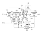
図1は、本実施形態による受信回路の構成例を示す図である。受信回路は、例えば、集積回路チップ内又はチップ間(装置内又は装置間)でビットレートの高い信号を送受信する高速入出力I/O)回路の受信回路である。受信回路は、高データレートの入力データ信号Diを基にクロック信号及びデータを再生(CDR:Clock and Data Recovery)する。 FIG. 1 is a diagram illustrating a configuration example of a receiving circuit according to the present embodiment. The reception circuit is, for example, a reception circuit of a high-speed input / output I / O circuit that transmits and receives a signal with a high bit rate within an integrated circuit chip or between chips (inside or between devices). The receiving circuit reproduces a clock signal and data (CDR: Clock and Data Recovery) based on the input data signal Di having a high data rate.
等化回路101は、等化係数Czを基に、入力データ信号Diを等化し、その等化した入力データ信号Di1をサンプリング回路102に出力する。受信回路は、送信回路から伝送路を介して、入力データ信号Diを入力する。送信回路が2値のパルス信号を送信すると、伝送路の特性により、受信回路は、パルス信号の立ち上がり速度及び立ち下がり速度が遅い入力データ信号Diを入力する。等化回路101は、伝送路の特性を除去するように、入力データ信号Diを等化することにより、送信回路の送信パルス信号に近付けた入力データ信号Di1を出力する。入力データ信号Di1は、入力データ信号Diに対して、立ち上がり速度及び/又は立ち下がり速度が速い信号である。
The
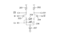
図2は、図1の等化回路101の構成例を示す回路図である。図1はシングルエンド信号の例を示すが、図2の等化回路101は差動信号の例を示す。差動入力データ信号Di及び/Diは、相互に位相が反転した信号である。差動入力データ信号Di1及び/Di1は、相互に位相が反転した信号である。等化回路101は、差動入力データ信号Di及び/Diを入力し、差動入力データ信号Di1及び/Di1を出力する。
FIG. 2 is a circuit diagram showing a configuration example of the
抵抗201は、電源電圧ノード及び入力データ信号/Di1のノード間に接続される。抵抗202は、電源電圧ノード及び入力データ信号Di1のノード間に接続される。nチャネル電界効果トランジスタ203は、ドレインが入力データ信号/Di1のノードに接続され、ゲートが入力データ信号Diのノードに接続される。nチャネル電界効果トランジスタ204は、ドレインが入力データ信号Di1のノードに接続され、ゲートが入力データ信号/Diのノードに接続される。可変抵抗205は、トランジスタ203のソース及びトランジスタ204のソース間に接続され、等化係数Czに応じて抵抗値が変化する。可変容量206は、トランジスタ203のソース及びトランジスタ204のソース間に接続され、等化係数Czに応じて容量値が変化する。定電流源207は、トランジスタ203及び204のソースの相互接続点とグランド電位ノードとの間に接続される。
図2では、等化回路101の例として、CTLE(Continuous Time Linear Equalizer)回路を示す。この回路は、差動入力トランジスタ203及び204のソース間の可変抵抗205により、低周波成分の利得を下げ、等価的に高周波成分を強調し、入力データ信号の高周波成分を復元する。強調する利得や周波数特性は、等化係数Czにより可変容量206の容量値及び/又は可変抵抗205の抵抗値を変えることにより調整される。
In FIG. 2, a CTLE (Continuous Time Linear Equalizer) circuit is shown as an example of the
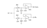
図1のサンプリング回路102は、入力データ信号Di1に対して、第1のクロック信号CK1に同期してバウンダリデータBsをサンプリングし、第2のクロック信号CK2に同期してセンタデータDs及びエラー用データEsをサンプリングする。
The
図3は、図1のサンプリング回路102の構成例を示す回路図である。スイッチ302は、第1のクロック信号CK1がハイレベルになると、入力データ信号Di1のノードを容量304に接続し、第1のクロック信号CK1がローレベルになると、入力データ信号Di1のノードを容量304から切り離す。スイッチ301は、第2のクロック信号CK2がハイレベルになると、入力データ信号Di1のノードを容量303に接続し、第2のクロック信号CK2がローレベルになると、入力データ信号Di1のノードを容量303から切り離す。オペアンプ306は、容量304の電圧を増幅して、バウンダリデータBsを出力する。オペアンプ305は、容量303の電圧を増幅して、センタデータDs及びエラー用データEsを出力する。センタデータDs及びエラー用データEsは、相互に同一のデータである。
FIG. 3 is a circuit diagram showing a configuration example of the
クロック信号CK1及びCK2は、相互に位相が反転した信号である。サンプリング回路102は、クロック信号CK1及びCK2によりインターリーブ動作する。図4(A)に示すように、サンプリング回路102は、クロック信号CK1の立ち上がりエッジに同期して、入力データ信号Di1をタイミングP1でサンプリングすることによりバウンダリデータ401(Bs)を出力し、クロック信号CK2の立ち上がりエッジに同期して、入力データ信号Di1をタイミングP2でサンプリングすることによりセンタデータDsを出力する。なお、インターリーブ数は、2に限定されるものではなく、2×n(nは整数)での構成が可能であり、回路の動作速度に応じて決定される。また、図4(A)では、2相クロック信号CK1及びCK2の例を示したが、その周波数を1/2にした4相クロック信号を用いてもよい。
The clock signals CK1 and CK2 are signals whose phases are reversed. The
図4(A)において、入力データ信号Di1の波形は、横軸が時間を表し、縦軸が振幅値を示す。横軸の時間は、ユニットインターバル(UI)で示す。1UIは、入力データ信号Di1の1ビット時間であり、隣接する2個のデータバウンダリ時刻(データ遷移時刻)の間の時間である。1[UI]の周期のデータは、「101010・・・」のデータ遷移状態を示す。2[UI]の周期のデータは、「11001100・・・」のデータ遷移状態を示す。タイミングP1は、隣接する2個のデータの境界のタイミングを示すバウンダリデータタイミングである。タイミングP2は、1個のデータのセンタのタイミングを示すセンタデータタイミングである。タイミングP1及びP2は、相互に0.5[UI]の位相差を有する。 4A, in the waveform of the input data signal Di1, the horizontal axis represents time, and the vertical axis represents the amplitude value. The time on the horizontal axis is indicated by a unit interval (UI). 1 UI is a 1-bit time of the input data signal Di1, and is a time between two adjacent data boundary times (data transition times). The data having a period of 1 [UI] indicates a data transition state of “101010. Data with a period of 2 [UI] indicates a data transition state of “11001100. Timing P1 is a boundary data timing indicating the timing of the boundary between two adjacent data. Timing P2 is center data timing indicating the timing of the center of one piece of data. The timings P1 and P2 have a phase difference of 0.5 [UI] from each other.
図1の判定帰還等化回路(DFE:Decision Feedback Equalizer)103は、等化係数Cdを用いて、サンプリング回路102によりサンプリングされたセンタデータDsを等化及び2値判定し、2値のセンタデータDdを出力する。センタデータDdは、「0」又は「1」の2値である。例えば、データ「1」は振幅値が正のデータであり、データ「0」は振幅値が負のデータである。等化回路101は一次等化回路であり、判定帰還等化回路103は二次等化回路である。
The decision feedback equalizer (DFE: Decision Feedback Equalizer) 103 in FIG. 1 equalizes and binary-determines the center data Ds sampled by the
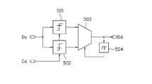
図5は、図1の判定帰還等化回路103の構成例を示す図である。判定帰還等化回路103は、等化係数Cdを入力し、第1の等化係数「+Cd」を比較回路501に与え、第2の等化係数「−Cd」を比較回路502に与える。比較回路501は、センタデータDsと第1の等化係数「+Cd」との比較結果を出力する。具体的には、比較回路501は、センタデータDsが第1の等化係数「+Cd]より大きい場合にはデータ「1」を出力し、センタデータDsが第1の等化係数「+Cd]より小さい場合にはデータ「0」を出力する。比較回路502は、センタデータDsと第2の等化係数「−Cd」との比較結果を出力する。具体的には、比較回路502は、センタデータDsが第2の等化係数「−Cd]より大きい場合にはデータ「1」を出力し、センタデータDsが第2の等化係数「−Cd]より小さい場合にはデータ「0」を出力する。セレクタ503は、フリップフロップ回路504に記憶されているデータが「1」の場合には、比較回路501の出力データを選択し、フリップフロップ回路504に記憶されているデータが「0」の場合には、比較回路502の出力データを選択し、2値データDdを出力する。フリップフロップ回路504は、セレクタ503の出力データDdを記憶する。すなわち、セレクタ503は、フリップフロップ回路504に記憶されている前回の出力データDdに応じて、比較回路501又は502の出力データを選択する。
FIG. 5 is a diagram illustrating a configuration example of the decision
図6(A)は、図4(A)に対応する図である。データ遷移601は、「11001100・・・」のデータパターンにおいて、前回のデータ「1」から今回のデータ「1」又は「0」への遷移を示す。この場合、データ遷移601の中心振幅値411は、振幅値「0」より上に位置する。したがって、前回のデータが「1」の場合には、比較回路501は、第1の等化係数411(=「+Cd」)より大きい場合にはデータ「1」を出力し、第1の等化係数411(=「+Cd」)より小さい場合にはデータ「0」を出力する。
FIG. 6A is a diagram corresponding to FIG. The
データ遷移602は、「11001100・・・」のデータパターンにおいて、前回のデータ「0」から今回のデータ「1」又は「0」への遷移を示す。この場合、データ遷移602の中心振幅値413は、振幅値「0」より下に位置する。したがって、前回のデータが「0」の場合には、比較回路502は、第2の等化係数413(=「−Cd」)より大きい場合にはデータ「1」を出力し、第2の等化係数413(=「−Cd」)より小さい場合にはデータ「0」を出力する。
The
図5の判定帰還等化回路103は、1タップの判定帰還等化回路である。セレクタ503は、前回の出力データDdに応じて選択することにより、高速処理が可能になる。なお、判定帰還等化回路103は、1タップに限定されるものではなく、複数タップでも実現可能である。例えば、2タップの判定帰還等化回路103の場合は、4個の比較回路501,502等を設け、1ビット前と2ビット前の出力データDdに応じて、4個の比較回路501,502等の出力データのうちの1個を選択する。同様に、mタップの判定帰還等化回路103の場合は、2m個の比較回路501及び502等が必要となる。
The decision
図6(A)はサンプリング回路102の出力データを示す図であり、図6(B)は判定帰還等化回路103の出力データを示す図である。図6(B)に示すように、判定帰還等化回路103は、振幅値「0」の閾値412を用いて、データ遷移601及び602のデータを判定していることと等価になる。図6(A)のタイミングP1のデータ401は、バウンダリデータBsである。図6(B)のタイミングP2のデータ403は、センタデータDdである。図6(A)のセンタデータタイミングP2は、データのセンタ位相に位置するが、図6(B)のセンタデータタイミングP2のデータ403は、データのセンタ位相より遅れた位置(右側の位置)にずれている。これは、判定帰還等化回路103の等化処理によるものである。判定帰還等化回路103は、データのセンタ位相のサンプリングデータを判定すれば判定エラー率が低くなるが、ずれたタイミングP2のサンプリングデータ403を判定すれば判定エラー率が増加してしまう。そこで、センタデータ403のサンプリングタイミングP2を調整することにより、判定帰還等化回路103の判定エラー率を低減する方法を、以下、説明する。
6A is a diagram illustrating output data of the
図1の第1の比較回路104は、サンプリング回路102によりサンプリングされたバウンダリデータBsを2値判定し、2値のバウンダリデータを出力する。具体的には、第1の比較回路104は、バウンダリデータBsの振幅値が「0」より大きい場合には「1」を出力し、バウンダリデータBsの振幅値が「0」より小さい場合には「0」を出力する。
The
第2の比較回路105は、サンプリング回路102によりサンプリングされたエラー用データEs(=センタデータDs)を閾値Ceと比較し、2値のエラー用データを出力する。具体的には、第2の比較回路105は、エラー用データEsの絶対値が閾値Ceより小さい場合にはエラー用データ「1」を出力し、エラー用データEsの絶対値が閾値Ceより大きい場合にはエラー用データ「0」を出力する。
The
逆多重化回路106は、判定帰還等化回路103、第1の比較回路104及び第2の比較回路105の出力データを逆多重化し、それぞれセンタデータDo、バウンダリデータBs1及びエラー用データEs1を出力する。すなわち、逆多重化回路106は、高周波数のシリアル信号を低周波数のパラレル信号に変換する。逆多重化回路106の出力データは、データレートが低くなるので、その後段の位相検出回路107、位相差演算回路109及び適応ロジック回路113は低速処理が可能になる。センタデータDoは、受信回路の出力データとなる。
The
図1の適応ロジック回路113は、センタデータDo及びエラー用データEs1を基に等化係数Cz、閾値Ce及び等化係数Cdを演算し、等化係数Cz、閾値Ce及び等化係数Cdを出力する。適応ロジック回路113は、例えばLMS(Least Mean Square)アルゴリズムなどで逐次的に等化係数Cdなどの最適化を行う。例えば、適応ロジック回路113は、次式により、n−1番目のサンプリングデータの等化係数Cd(n−1)、n番目のサンプリングデータのエラー用データEs(n)及びn−1番目のセンタデータDo(n−1)を用いて、n番目のサンプリングデータの等化係数Cd(n)を導出することができる。ここで、μは、ステップを示す。また、適応ロジック回路113は、等化係数Cdと同様に、等化係数Czを演算する。
Cd(n)=Cd(n−1)−μ×Es1(n)×Do(n−1)
The
Cd (n) = Cd (n−1) −μ × Es1 (n) × Do (n−1)
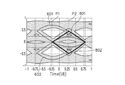
図7(A)は、図6(A)に対応し、サンプリング回路102の出力を示す図である。バウンダリデータ401は、データ遷移601及び602が振幅値「0」でクロスするゼロクロス点の位相に位置する。そのゼロクロス点付近のデータ遷移601及び602の実線部分は、直線に近似することができる。ここで、第1の等化係数411は、等化係数Cdであり、既知の値である。ここで、データ遷移601及び602の実線部分の直線の傾きは、スルーレート(波形の傾き)である。したがって、その直線の傾きが分かれば、その直線の傾き及び等化係数Cdを基に位相差702を算出することができる。
FIG. 7A corresponds to FIG. 6A and shows the output of the
図7(B)は、図6(B)に対応し、判定帰還等化回路103の出力を示す図であり、センタデータ403は、上記のように、判定帰還等化回路103の等化処理により、データのセンタ位相に対して位相差702のずれを有する。この位相差702は、上記のように、直線の傾き及び等化係数Cdを基に算出することができる。センタデータ403の位相を位相差702だけ早めることにより、データのセンタ位相のセンタデータ402を得ることが可能になる。判定帰還等化回路103は、データセンタ位相のセンタデータ402を判定することにより、判定エラー率を低減することができる。
FIG. 7B corresponds to FIG. 6B and shows the output of the decision
図1の位相差演算回路109は、上記の位相差702を演算する。具体的には、位相差演算回路109は、判定帰還等化回路103の等化係数Cd、エラー用データEs1及びセンタデータDoを基に、判定帰還等化回路103の出力データの位相差Shを演算する。位相差Shは、図7(B)の位相差702に対応する。
The phase
図8は、図7(A)に対応し、図1の位相差演算回路109の演算方法を説明するための図である。位相差演算回路109は、サンプリングタイミングP2において、データ遷移601及び602の直線近似のクロスポイント801及び802を検出する。タイミングP2の0.5[UI]後では、データ遷移601及び602が振幅値「0」でクロスする。データ遷移601及び602の上記のクロスポイント801及び802を通る実線部分は、直線に近似することができる。適応ロジック回路113が閾値Ceを変化させ、第2の比較回路105がエラー用データEs(センタデータDs)の絶対値と閾値Ceとの比較を行い、位相差演算回路109は第2の比較回路105の比較結果を入力する。その結果、位相差演算回路109は、タイミングP2のセンタデータDsが+Cs〜−Csの範囲内にあるか否かを知ることができる。閾値Csを変えることにより、位相差演算回路109は、クロスポイント801及び802の振幅値を知ることができる。閾値Csは、適応ロジック回路113のエラーモニタ用の閾値と併用可能である。
FIG. 8 corresponds to FIG. 7A and is a diagram for explaining a calculation method of the phase
例えば、クロスポイント801の振幅値は、「0.42」として検出される。また、位相差演算回路109は、適応ロジック回路113から等化係数Cdとして「0.22」を入力する。この場合、クロスポイント801及びその0.5[UI]後のゼロクロスポイントを結ぶ実線の直線のスルーレート(傾き)は、0.42/0.5=0.84として、位相差演算回路109により演算される。次に、位相差演算回路109は、0.22/0.84=0.26の演算により位相差702(Sh)を演算する。
For example, the amplitude value of the
具体的には、位相差演算回路109は、例えば以下の演算を行うことにより、位相差Shを導出する。ここで、Cdは等化係数であり、ACはクロスポイント801又は802の振幅値の絶対値である。
Sh=Cd/(2×AC)
Specifically, the phase
Sh = Cd / (2 × AC)
図1の位相検出回路107は、センタデータDo及びバウンダリデータBs1を入力し、センタデータDo及びバウンダリデータBs1を基に入力データ信号Diの位相情報UDを検出して出力する。
The
図9(A)は、図1の位相検出回路107の構成例を示す回路図である。位相検出回路107は、排他的論理和(XOR)回路901及び902を有する。図9(C)及び(D)に示すように、センタデータDo[0]は、第1のサイクルのセンタデータDoである。センタデータDo[1]は、その次の第2のサイクルのセンタデータDoである。バウンダリデータBs1[0]は、センタデータDo[0]及びDo[1]の間のバウンダリデータBs1である。排他的論理和回路901は、センタデータDo[1]及びバウンダリデータBs1[0]の排他的論理和データをビットUPとして出力する。排他的論理和回路902は、センタデータDo[0]及びバウンダリデータBs1[0]の排他的論理和データをビットDNとして出力する。位相検出回路107は、図9(B)に示すように、データDo[0]、Do[1]及びBs1[0]を入力し、2ビット位相データUP及びDNを出力する。2ビット位相データUP及びDNは、図1の位相情報UDに対応する。
FIG. 9A is a circuit diagram illustrating a configuration example of the
図9(C)は、ダウンダリデータBs1[0]の位相がバウンダリ位相(データ遷移位相)より早い場合の例を示す図である。例えば、センタデータDo[0]及びバウンダリデータBs1[0]が「1」であり、その次のセンタデータDo[1]が「0」である。この場合は、ダウンダリデータBs1[0]の位相がバウンダリ位相(データ遷移位相)より早いので、サンプリング位相を遅らせるため、「1」のダウンビットDNが出力される。 FIG. 9C is a diagram illustrating an example in which the phase of the down-boundary data Bs1 [0] is earlier than the boundary phase (data transition phase). For example, the center data Do [0] and the boundary data Bs1 [0] are “1”, and the next center data Do [1] is “0”. In this case, since the phase of the down boundary data Bs1 [0] is earlier than the boundary phase (data transition phase), the down bit DN of “1” is output to delay the sampling phase.
図9(D)は、ダウンダリデータBs1[0]の位相がバウンダリ位相(データ遷移位相)より遅い場合の例を示す図である。例えば、センタデータDo[0]が「0」であり、バウンダリデータBs1[0]及びその次のセンタデータDo[1]が「1」である。この場合は、ダウンダリデータBs1[0]の位相がバウンダリ位相(データ遷移位相)より遅いので、サンプリング位相を早めるため、「1」のアップビットUPが出力される。 FIG. 9D is a diagram illustrating an example in which the phase of the down data Bs1 [0] is later than the boundary phase (data transition phase). For example, the center data Do [0] is “0”, the boundary data Bs1 [0] and the next center data Do [1] are “1”. In this case, since the phase of the down data Bs1 [0] is later than the boundary phase (data transition phase), the up bit UP of “1” is output to advance the sampling phase.
以上のように、位相検出回路107は、データ値の変化があったときにバウンダリデータBs1[0]がその前のセンタデータDo[0]又はその後のセンタデータDo[1]のどちらと同じかにより位相のずれを検出する。なお、図9(A)〜(D)では、連続する2ビットデータ間の構成のみ示しているが、実際には逆多重化回路106により複数ビットのデータとなっており、それぞれのデータ間で位相検出を行う。
As described above, the
図1のフィルタ108は、ローパスフィルタであり、位相検出回路107により検出された位相情報UDをローパスフィルタリングし、位相情報Phを出力する。フィルタ108は、高周波ノイズを除去し、平均化した位相情報Phを出力することができる。フィルタ108を用いることにより、位相情報Phの急激な変化を防止し、位相情報Phの変化を緩やかにすることができる。
A
第1の位相調整回路111は、位相情報Phに応じて、基準クロック信号CKを用いて第1のクロック信号CK1の位相を調整する。上記のアップビットUPが「1」である場合には、第1のクロック信号CK1の位相が早くなるように制御される。上記のダウンビットDNが「1」である場合には、第1のクロック信号CK1の位相が遅くなるように制御される。これにより、図9(C)及び(D)のバウンダリデータBs1[0]の位相がバウンダリ位相(データ遷移位相)に一致するように制御される。 The first phase adjustment circuit 111 adjusts the phase of the first clock signal CK1 using the reference clock signal CK according to the phase information Ph. When the up bit UP is “1”, control is performed so that the phase of the first clock signal CK1 is advanced. When the down bit DN is “1”, the phase of the first clock signal CK1 is controlled to be delayed. Thus, the phase of the boundary data Bs1 [0] in FIGS. 9C and 9D is controlled so as to coincide with the boundary phase (data transition phase).
減算器110は、位相情報Phと0.5[UI]とを加算し、その加算結果から位相差Shを減算することにより、位相情報Ph1を出力する。第2の位相調整回路112は、位相情報Ph1に応じて、基準クロック信号CKを用いて第2のクロック信号CK2の位相を調整する。上記と同様に、上記のアップビットUPが「1」である場合には、第2のクロック信号CK2の位相が早くなるように制御される。上記のダウンビットDNが「1」である場合には、第2のクロック信号CK2の位相が遅くなるように制御される。また、図4(A)に示すように、センタデータ位相P2は、バウンダリデータ位相P1に対して0.5[UI]遅れた位相であるので、減算器110は0.5[UI]を加算する。また、位相差Shは、図7(B)の位相差702に対応する。図7(B)に示すように、減算器110は位相差702(Sh)減算することにより、センタデータ403の位相を適切なセンタデータ402の位相に変更することができる。
The
図4(A)において、第1のクロック信号CK1及び第2のクロック信号CK2は位相調整前のクロック信号の例を示し、第1のクロック信号CK1a及び第2のクロック信号CK2aは位相調整後のクロック信号の例を示す。位相調整前では、第2のクロック信号CK2は、第1のクロック信号CK1に対して0.5[UI]遅れている。ここで、位相差演算回路109により位相差Shが演算された場合、位相調整後の第1のクロック信号CK1aは、位相調整前の第1のクロック信号CK1と位相が同じである。これに対し、位相調整後の第2のクロック信号CK2aは、位相調整前の第2のクロック信号CK2に対して位相差Sh進んだ位相に調整される。位相調整後、サンプリング回路102は、第1のクロック信号CK1aの立ち上がり位相P1に同期してバウンダリデータBsをサンプリングし、第2のクロック信号CK2aの立ち上がり位相P3に同期してセンタデータDs及びエラー用データEsをサンプリングする。
In FIG. 4A, the first clock signal CK1 and the second clock signal CK2 are examples of clock signals before phase adjustment, and the first clock signal CK1a and the second clock signal CK2a are after phase adjustment. An example of a clock signal is shown. Before the phase adjustment, the second clock signal CK2 is delayed by 0.5 [UI] with respect to the first clock signal CK1. Here, when the phase difference Sh is calculated by the phase
図4(B)は、図7(B)に対応し、位相調整後の第1のクロック信号CK1a及び第2のクロック信号CK2aによりサンプリングした場合の判定帰還等化回路103の出力例を示す図である。判定帰還等化回路103は、位相P3でサンプリングされたセンタデータ402の判定を行う。センタデータ402は、センタ位相P3に調整されているので、判定帰還等化回路103の判定エラー率を低減することができる。
FIG. 4B corresponds to FIG. 7B and shows an output example of the decision
図10は、図1の第1の位相調整回路111の構成例を示す回路図である。第1の位相調整回路111は、可変遅延回路により構成される。複数のバッファの直列接続回路1001は、遅延回路であり、基準クロック信号CKを遅延する。セレクタ1002は、位相情報Phに応じて、複数のバッファ1001のうちのいずれかの出力信号を選択し、第1のクロック信号CK1を出力する。第1のクロック信号CK1は、位相情報Phに応じた遅延時間だけ基準クロック信号CKを遅延した信号になる。
FIG. 10 is a circuit diagram showing a configuration example of the first phase adjustment circuit 111 of FIG. The first phase adjustment circuit 111 is configured by a variable delay circuit. A
図11は、図1の第1の位相調整回路111の他の構成例を示す回路図である。第1の位相調整回路111は、位相補間回路により構成される。4相基準クロック信号CK0,CL90,CL180,CL270は、図1の基準クロック信号CKに対応する。クロック信号CK0は0度の位相のクロック信号であり、クロック信号CL90は90度の位相のクロック信号であり、クロック信号CL180は180度の位相のクロック信号であり、クロック信号CL270は270度の位相のクロック信号である。差動アンプ1101は、電流源1103に接続され、差動クロック信号CL0及びCL180を増幅し、ノードN1及びN2の差動クロック信号を出力する。差動アンプ1102は、電流源1104に接続され、差動クロック信号CL90及びCL270を増幅し、ノードN1及びN2の差動クロック信号を出力する。差動アンプ1105は、ノードN1及びN2の差動クロック信号を増幅し、差動クロック信号CK1及び/CK1を出力する。差動クロック信号CK1及び/CK1は、相互に位相が反転した信号であり、図1の第1のクロック信号CK1に対応する。
FIG. 11 is a circuit diagram showing another configuration example of the first phase adjustment circuit 111 of FIG. The first phase adjustment circuit 111 is configured by a phase interpolation circuit. The four-phase reference clock signals CK0, CL90, CL180, and CL270 correspond to the reference clock signal CK in FIG. The clock signal CK0 is a clock signal having a phase of 0 degrees, the clock signal CL90 is a clock signal having a phase of 90 degrees, the clock signal CL180 is a clock signal having a phase of 180 degrees, and the clock signal CL270 is a phase of 270 degrees. Clock signal. The
電流源1103及び1104は、位相情報Phに応じて、電流比が制御される。この電流比に応じた重み付けで、差動アンプ1101の出力信号と差動アンプ1102の出力信号とがノードN1及びN2で加算される。
The current ratios of the
電流源1103及び1104の電流比が1:0の場合、第1のクロック信号CK1は、0度のクロック信号CL0と同じ位相になる。また、第1のクロック信号/CK1は、180度のクロック信号CL180と同じ位相になる。
When the current ratio between the
また、電流源1103及び1104の電流比が0:1の場合、第1のクロック信号CK1は、90度のクロック信号CL90と同じ位相になる。また、第1のクロック信号/CK1は、270度のクロック信号CL270と同じ位相になる。
When the current ratio between the
上記のように、位相情報Phに応じて、電流源1103及び1104の電流比を制御することにより、0度〜360度の任意の位相の第1のクロック信号CK1又は/CK1を生成することができる。
As described above, by controlling the current ratio of the
上記では、第1の位相調整回路111の構成を例に説明したが、第2の位相調整回路112の構成も第1の位相調整回路111の構成と同様である。 In the above, the configuration of the first phase adjustment circuit 111 has been described as an example. However, the configuration of the second phase adjustment circuit 112 is the same as the configuration of the first phase adjustment circuit 111.
図12(A)〜(C)は、図1の受信回路の収束性を説明するための図である。図12(A)は判定帰還等化回路103の等化係数Cdが小さい場合を示し、図12(B)は判定帰還等化回路103の等化係数Cdが最適値である場合を示し、図12(C)は判定帰還等化回路103の等化係数Cdが大きい場合を示す。等化係数Cdは、サンプリング位相において、データ遷移601及び602で囲まれる領域の振幅方向の開口が最大となるように調整される。すなわち、サンプリング位相毎に収束する等化係数Cdが異なる。逆に言えば、等化係数Cd毎に収束する位相が異なるとも言える。等化係数Cdが収束する位相を係数収束位相1201として示す。位相1202は、その時のスルーレートから計算され、シフトされたサンプリング位相を示す。図12(A)の等化係数Cdが小さい時、データ遷移602の波形の立ち上がりのスルーレートが小さく、サンプリング位相1202が係数収束位相1201より左となり、等化係数Cdがアップ方向に制御される。図12(C)の等化係数Cdが大きい時は、その逆で、データ遷移601の波形の立ち下がりのスルーレートが小さく、サンプリング位相1202が係数収束位相1201より右となり、等化係数Cdがダウン方向に制御される。最終的には、図12(B)のように、データ遷移602の波形の立ち上がりとデータ遷移601の波形の立ち下がりのスルーレートが等しくなる位相1201及び1202に収束するので、安定的に動作する。図12(B)では、データ遷移601及び602で囲まれる領域の開口の面積が最大となる位相1202及び等化係数Cdに収束する。
12A to 12C are diagrams for explaining the convergence of the receiving circuit in FIG. 12A shows a case where the equalization coefficient Cd of the decision
図13(A)〜(F)は、図12(A)〜(C)に対応し、図1の受信回路の収束性のシミュレーション結果を示す図であり、それぞれ等化係数Cdが0、0.1、0.2、0.3、0.4、0.5の場合を示す。係数収束位相AAでサンプリングすると、等化係数CdのアップUP及びダウンDNの遷移確率が等しくなり、収束する。位相差演算回路109を設けない場合、図13(C)の等化係数Cdが0.2の状態で収束する。この場合、図6(B)と同様に、係数収束位相AAがセンタ位相より遅れているので、判定エラー率が高くなってしまう。
FIGS. 13A to 13F correspond to FIGS. 12A to 12C and are graphs showing simulation results of convergence of the receiving circuit of FIG. 1, and equalization coefficients Cd are 0 and 0, respectively. .1, 0.2, 0.3, 0.4, 0.5 are shown. When sampling is performed at the coefficient convergence phase AA, the transition probabilities of up-up and down-DN of the equalization coefficient Cd become equal and converge. When the phase
これに対し、位相差演算回路109を設けた場合には、図13(A)〜(D)の等化係数Cdが0.1〜0.3の場合には、等化係数CdがアップUPに制御され、図13(F)の等化係数が0.5の場合には、等化係数CdがダウンDNに制御される。等化係数Cdが小さいときのサンプリング位相では、等化係数CdはアップUPに制御され、等化係数Cdが大きい時のサンプリング位相では、等化係数CdはダウンDNに制御される。最終的には、図13(E)の等化係数Cdが0.4の状態に収束し、図4(B)のように、判定エラー率が低くなる。
In contrast, when the phase
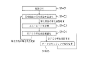
図14は、図1の受信回路の制御方法を示すフローチャートである。ステップS1401では、受信回路の電源がオンになる。次に、ステップS1402では、適応ロジック回路113は、等化回路101の等化係数Czの最適化のためのフィードバック処理により、等化回路101の等化係数Czを収束させる。この時、適応ロジック回路113は、位相差演算回路109のスルーレート計算用にモニタするデータにおいて線形性がよくなるように等化係数を収束させることにより、位相差Shの検出精度を向上させることができる。なお、等化回路101の等化は、上記の直線近似の精度をより向上させるために、「1010」の周期のデータの等化精度までは必要ないが、「0011」及び「1100」の周期のデータの等化精度があることが好ましい。
FIG. 14 is a flowchart showing a control method of the receiving circuit of FIG. In step S1401, the receiving circuit is turned on. Next, in step S1402, the
等化係数Czの収束後、ステップS1403では、位相差演算回路109は、スルーレートの計算を行う。その後、ステップS1404では、適応ロジック回路113は、判定帰還等化回路103の等化係数Cdの最適化処理を開始し、等化係数Cdを生成する。
After convergence of the equalization coefficient Cz, in step S1403, the phase
等化係数Cdが更新されると、ステップS1405では、第2の位相調整回路112は、位相差演算回路109により演算された位相差Shに応じて、第2のクロック信号CK2の位相を調整し、サンプリング回路102はセンタデータDs及びエラー用データEsのサンプリング位相を変更する。その後、ステップS1404の処理に戻る。
When the equalization coefficient Cd is updated, in step S1405, the second phase adjustment circuit 112 adjusts the phase of the second clock signal CK2 according to the phase difference Sh calculated by the phase
ステップS1404において、適応ロジック回路113が等化回路101の等化係数Czを更新した場合、ステップS1402の処理に戻る。
If the
本実施形態の制御方法は、上記の制御方法に限定されない。例えば、ステップS1402の等化回路101の等化係数Czの最適化処理は初期動作時に行い、それ以降はエラーが発生するまで等化回路101の等化係数Czの更新を行わないようにしてもよい。適応ロジック回路113は、ステップS1404の判定帰還等化回路103の等化係数Cdの最適化処理において、エラーが発生した場合には、ステップS1402に戻り、等化回路101の等化係数Czの更新を行う。
The control method of this embodiment is not limited to the above control method. For example, the optimization process of the equalization coefficient Cz of the
また、初期動作時に、トレーニングシーケンスとして、等化回路101は、「0011」又は「1100」の特定データパターンを含む入力データ信号Diを入力することが好ましい。入力データ信号Diとして、スルーレートの検出に有利な「0011」又は「1100」のデータパターンを多く入力することにより、初期動作のキャリブレーションに要する時間を短縮することができる。入力データ信号Diは、検出精度を向上させるために特定のデータパターンを多く含むことが好ましいが、これに限定されるものではない。
In the initial operation, the
本実施形態によれば、位相差演算回路109により演算された位相差Shを基に第2のクロック信号CK2の位相を調整することにより、適切な位相のセンタデータDsに対して判定を行うことができ、判定エラー率を低減することができる。
According to the present embodiment, the center data Ds having an appropriate phase is determined by adjusting the phase of the second clock signal CK2 based on the phase difference Sh calculated by the phase
なお、上記実施形態は、何れも本発明を実施するにあたっての具体化の例を示したものに過ぎず、これらによって本発明の技術的範囲が限定的に解釈されてはならないものである。すなわち、本発明はその技術思想、又はその主要な特徴から逸脱することなく、様々な形で実施することができる。 The above-described embodiments are merely examples of implementation in carrying out the present invention, and the technical scope of the present invention should not be construed in a limited manner. That is, the present invention can be implemented in various forms without departing from the technical idea or the main features thereof.
101 等化回路
102 サンプリング回路
103 判定帰還等化回路
104 第1の比較回路
105 第2の比較回路
106 逆多重化回路
107 位相検出回路
108 フィルタ
109 位相差演算回路
110 減算器
111 第1の位相調整回路
112 第2の位相調整回路
113 適応ロジック回路
101
Claims (9)
等化係数を用いて、前記サンプリング回路によりサンプリングされたセンタデータを等化及び2値判定する判定帰還等化回路と、
前記サンプリング回路によりサンプリングされたバウンダリデータを2値判定する第1の比較回路と、
前記判定帰還等化回路及び前記第1の比較回路の出力データを基に前記入力データ信号の位相情報を検出する位相検出回路と、
前記判定帰還等化回路の等化係数を基に前記判定帰還等化回路の出力データの位相差を演算する位相差演算回路と、
前記位相検出回路により検出された位相情報を基に前記第1のクロック信号の位相を調整する第1の位相調整回路と、
前記位相検出回路により検出された位相情報及び前記位相差演算回路により演算された位相差を基に前記第2のクロック信号の位相を調整する第2の位相調整回路と
を有することを特徴とする受信回路。 A sampling circuit that samples boundary data in synchronization with a first clock signal and samples center data in synchronization with a second clock signal with respect to an input data signal;
A decision feedback equalization circuit that equalizes and binary-determines the center data sampled by the sampling circuit using an equalization coefficient;
A first comparison circuit for binary-determining boundary data sampled by the sampling circuit;
A phase detection circuit for detecting phase information of the input data signal based on output data of the decision feedback equalization circuit and the first comparison circuit;
A phase difference calculation circuit for calculating a phase difference of output data of the determination feedback equalization circuit based on an equalization coefficient of the determination feedback equalization circuit;
A first phase adjustment circuit for adjusting a phase of the first clock signal based on phase information detected by the phase detection circuit;
And a second phase adjustment circuit that adjusts the phase of the second clock signal based on the phase information detected by the phase detection circuit and the phase difference calculated by the phase difference calculation circuit. Receiver circuit.
前記位相差演算回路は、前記判定帰還等化回路の等化係数及び前記第2の比較回路の比較結果を基に前記判定帰還等化回路の出力データの位相差を演算することを特徴とする請求項1記載の受信回路。 And a second comparison circuit for comparing the center data sampled by the sampling circuit with a threshold value.
The phase difference calculation circuit calculates a phase difference of output data of the decision feedback equalization circuit based on an equalization coefficient of the decision feedback equalization circuit and a comparison result of the second comparison circuit. The receiving circuit according to claim 1.
前記判定帰還等化回路は、前回の出力データに応じて、前記サンプリング回路によりサンプリングされたセンタデータと前記第1の等化係数との比較結果、又は前記サンプリング回路によりサンプリングされたセンタデータと前記第2の等化係数との比較結果を出力することを特徴とする請求項1又は2記載の受信回路。 The equalization coefficient has a first equalization coefficient and a second equalization coefficient,
The determination feedback equalization circuit is configured to compare the center data sampled by the sampling circuit with the first equalization coefficient or the center data sampled by the sampling circuit according to the previous output data 3. The receiving circuit according to claim 1, wherein a comparison result with the second equalization coefficient is output.
前記サンプリング回路は、前記等化回路により等化された入力データ信号を入力することを特徴とする請求項1〜4のいずれか1項に記載の受信回路。 Furthermore, it has an equalization circuit for equalizing the input data signal,
The receiving circuit according to claim 1, wherein the sampling circuit inputs an input data signal equalized by the equalizing circuit.
前記第1の位相調整回路は、前記フィルタによりフィルタリングされた位相を基に前記第1のクロック信号の位相を調整し、
前記第2の位相調整回路は、前記フィルタによりフィルタリングされた位相及び前記位相差演算回路により演算された位相差を基に前記第2のクロック信号の位相を調整することを特徴とする請求項1〜5のいずれか1項に記載の受信回路。 Furthermore, it has a filter for filtering the phase information detected by the phase detection circuit,
The first phase adjustment circuit adjusts a phase of the first clock signal based on a phase filtered by the filter;
2. The second phase adjustment circuit adjusts the phase of the second clock signal based on the phase filtered by the filter and the phase difference calculated by the phase difference calculation circuit. The receiving circuit according to any one of?
前記位相検出回路は、前記逆多重化回路の出力データを基に前記入力データ信号の位相情報を検出することを特徴とする請求項1〜7のいずれか1項に記載の受信回路。 And a demultiplexing circuit that demultiplexes output data of the decision feedback equalization circuit and the first comparison circuit,
The receiving circuit according to claim 1, wherein the phase detection circuit detects phase information of the input data signal based on output data of the demultiplexing circuit.
等化係数を用いて、前記サンプリング回路によりサンプリングされたセンタデータを等化及び2値判定する判定帰還等化回路と、
前記サンプリング回路によりサンプリングされたバウンダリデータを2値判定する第1の比較回路と、
前記判定帰還等化回路及び前記第1の比較回路の出力データを基に前記入力データ信号の位相情報を検出する位相検出回路とを有する受信回路の制御方法であって、
前記判定帰還等化回路の等化係数を基に前記判定帰還等化回路の出力データの位相差を演算し、
前記位相検出回路により検出された位相情報を基に前記第1のクロック信号の位相を調整し、
前記位相検出回路により検出された位相情報及び前記演算された位相差を基に前記第2のクロック信号の位相を調整することを特徴とする受信回路の制御方法。 A sampling circuit that samples boundary data in synchronization with a first clock signal and samples center data in synchronization with a second clock signal with respect to an input data signal;
A decision feedback equalization circuit that equalizes and binary-determines the center data sampled by the sampling circuit using an equalization coefficient;
A first comparison circuit for binary-determining boundary data sampled by the sampling circuit;
A control method of a receiving circuit comprising: a phase detection circuit that detects phase information of the input data signal based on output data of the decision feedback equalization circuit and the first comparison circuit,
Calculate the phase difference of the output data of the decision feedback equalization circuit based on the equalization coefficient of the decision feedback equalization circuit,
Adjusting the phase of the first clock signal based on the phase information detected by the phase detection circuit;
A method for controlling a receiving circuit, comprising: adjusting a phase of the second clock signal based on phase information detected by the phase detection circuit and the calculated phase difference.
Priority Applications (2)
| Application Number | Priority Date | Filing Date | Title |
|---|---|---|---|
| JP2013077887A JP6079388B2 (en) | 2013-04-03 | 2013-04-03 | Reception circuit and control method thereof |
| US14/173,515 US8791735B1 (en) | 2013-04-03 | 2014-02-05 | Receiving circuit and control method of receiving circuit |
Applications Claiming Priority (1)
| Application Number | Priority Date | Filing Date | Title |
|---|---|---|---|
| JP2013077887A JP6079388B2 (en) | 2013-04-03 | 2013-04-03 | Reception circuit and control method thereof |
Publications (2)
| Publication Number | Publication Date |
|---|---|
| JP2014204234A JP2014204234A (en) | 2014-10-27 |
| JP6079388B2 true JP6079388B2 (en) | 2017-02-15 |
Family
ID=52354331
Family Applications (1)
| Application Number | Title | Priority Date | Filing Date |
|---|---|---|---|
| JP2013077887A Active JP6079388B2 (en) | 2013-04-03 | 2013-04-03 | Reception circuit and control method thereof |
Country Status (2)
| Country | Link |
|---|---|
| US (1) | US8791735B1 (en) |
| JP (1) | JP6079388B2 (en) |
Families Citing this family (75)
| Publication number | Priority date | Publication date | Assignee | Title |
|---|---|---|---|---|
| US9288082B1 (en) | 2010-05-20 | 2016-03-15 | Kandou Labs, S.A. | Circuits for efficient detection of vector signaling codes for chip-to-chip communication using sums of differences |
| US9251873B1 (en) | 2010-05-20 | 2016-02-02 | Kandou Labs, S.A. | Methods and systems for pin-efficient memory controller interface using vector signaling codes for chip-to-chip communications |
| US9077386B1 (en) | 2010-05-20 | 2015-07-07 | Kandou Labs, S.A. | Methods and systems for selection of unions of vector signaling codes for power and pin efficient chip-to-chip communication |
| US9231802B2 (en) | 2012-12-26 | 2016-01-05 | Nvidia Corporation | Influence clock data recovery settling point by applying decision feedback equalization to a crossing sample |
| WO2014172377A1 (en) | 2013-04-16 | 2014-10-23 | Kandou Labs, S.A. | Methods and systems for high bandwidth communications interface |
| US9762381B2 (en) * | 2013-07-03 | 2017-09-12 | Nvidia Corporation | Adaptation of crossing DFE tap weight |
| JP6244722B2 (en) * | 2013-08-01 | 2017-12-13 | 富士通株式会社 | CDR circuit |
| US9413518B2 (en) | 2013-08-12 | 2016-08-09 | Nvidia Corporation | Clock data recovery circuit |
| JP6179334B2 (en) * | 2013-10-10 | 2017-08-16 | 富士通株式会社 | Receiver and data interpolation method |
| US9806761B1 (en) | 2014-01-31 | 2017-10-31 | Kandou Labs, S.A. | Methods and systems for reduction of nearest-neighbor crosstalk |
| JP6317474B2 (en) | 2014-02-02 | 2018-04-25 | カンドウ ラボズ ソシエテ アノニム | Method and apparatus for low power chip-to-chip communication using constrained ISI ratio |
| EP3111607B1 (en) | 2014-02-28 | 2020-04-08 | Kandou Labs SA | Clock-embedded vector signaling codes |
| EP3138253A4 (en) | 2014-07-10 | 2018-01-10 | Kandou Labs S.A. | Vector signaling codes with increased signal to noise characteristics |
| WO2016019384A1 (en) | 2014-08-01 | 2016-02-04 | Kandou Labs, S.A. | Orthogonal differential vector signaling codes with embedded clock |
| JP6402565B2 (en) * | 2014-10-02 | 2018-10-10 | 富士通株式会社 | Reception circuit and control method thereof |
| US9674014B2 (en) | 2014-10-22 | 2017-06-06 | Kandou Labs, S.A. | Method and apparatus for high speed chip-to-chip communications |
| JP6428279B2 (en) * | 2015-01-13 | 2018-11-28 | 株式会社ソシオネクスト | Reception circuit, transmission / reception circuit, and integrated circuit |
| US10341145B2 (en) * | 2015-03-03 | 2019-07-02 | Intel Corporation | Low power high speed receiver with reduced decision feedback equalizer samplers |
| JP6488863B2 (en) * | 2015-05-07 | 2019-03-27 | 富士通株式会社 | Receiving circuit and control method of receiving circuit |
| US9755819B2 (en) * | 2015-07-01 | 2017-09-05 | Rambus Inc. | Phase calibration of clock signals |
| US10055372B2 (en) | 2015-11-25 | 2018-08-21 | Kandou Labs, S.A. | Orthogonal differential vector signaling codes with embedded clock |
| WO2017132292A1 (en) | 2016-01-25 | 2017-08-03 | Kandou Labs, S.A. | Voltage sampler driver with enhanced high-frequency gain |
| WO2017175365A1 (en) * | 2016-04-08 | 2017-10-12 | 株式会社日立製作所 | Electric signal transmission apparatus |
| CN115085727A (en) | 2016-04-22 | 2022-09-20 | 康杜实验室公司 | High performance phase locked loop |
| WO2017185070A1 (en) | 2016-04-22 | 2017-10-26 | Kandou Labs, S.A. | Calibration apparatus and method for sampler with adjustable high frequency gain |
| US10003454B2 (en) | 2016-04-22 | 2018-06-19 | Kandou Labs, S.A. | Sampler with low input kickback |
| US10153591B2 (en) | 2016-04-28 | 2018-12-11 | Kandou Labs, S.A. | Skew-resistant multi-wire channel |
| US10333741B2 (en) | 2016-04-28 | 2019-06-25 | Kandou Labs, S.A. | Vector signaling codes for densely-routed wire groups |
| US10193716B2 (en) | 2016-04-28 | 2019-01-29 | Kandou Labs, S.A. | Clock data recovery with decision feedback equalization |
| JP6086639B1 (en) * | 2016-05-12 | 2017-03-01 | 株式会社セレブレクス | Data receiver |
| US9906358B1 (en) | 2016-08-31 | 2018-02-27 | Kandou Labs, S.A. | Lock detector for phase lock loop |
| US10411922B2 (en) | 2016-09-16 | 2019-09-10 | Kandou Labs, S.A. | Data-driven phase detector element for phase locked loops |
| JP6697990B2 (en) * | 2016-09-16 | 2020-05-27 | ルネサスエレクトロニクス株式会社 | Semiconductor device |
| US10200188B2 (en) | 2016-10-21 | 2019-02-05 | Kandou Labs, S.A. | Quadrature and duty cycle error correction in matrix phase lock loop |
| US10372665B2 (en) | 2016-10-24 | 2019-08-06 | Kandou Labs, S.A. | Multiphase data receiver with distributed DFE |
| US10200218B2 (en) | 2016-10-24 | 2019-02-05 | Kandou Labs, S.A. | Multi-stage sampler with increased gain |
| JP6839354B2 (en) * | 2017-02-03 | 2021-03-10 | 富士通株式会社 | CDR circuit and receiving circuit |
| JP6912702B2 (en) * | 2017-02-20 | 2021-08-04 | 富士通株式会社 | CDR circuit and receiving circuit |
| JP7007809B2 (en) * | 2017-03-24 | 2022-02-10 | シナプティクス・ジャパン合同会社 | Digital signal transmission device, clock signal transmission device, and reception circuit |
| CN115333530A (en) | 2017-05-22 | 2022-11-11 | 康杜实验室公司 | Multi-mode data-driven clock recovery method and apparatus |
| US10326620B2 (en) | 2017-05-31 | 2019-06-18 | Kandou Labs, S.A. | Methods and systems for background calibration of multi-phase parallel receivers |
| US10203226B1 (en) | 2017-08-11 | 2019-02-12 | Kandou Labs, S.A. | Phase interpolation circuit |
| CN109687951B (en) * | 2017-10-19 | 2021-06-01 | 创意电子股份有限公司 | Sampling phase adjusting device and adjusting method thereof |
| CN107920038A (en) * | 2017-10-31 | 2018-04-17 | 北京集创北方科技股份有限公司 | Balanced device adjusting method and device |
| US10347283B2 (en) | 2017-11-02 | 2019-07-09 | Kandou Labs, S.A. | Clock data recovery in multilane data receiver |
| EP3721561B1 (en) | 2017-12-07 | 2024-04-17 | Kandou Labs S.A. | Decision feedback equalization correction of eye scope measurements |
| US10326623B1 (en) | 2017-12-08 | 2019-06-18 | Kandou Labs, S.A. | Methods and systems for providing multi-stage distributed decision feedback equalization |
| US10554380B2 (en) | 2018-01-26 | 2020-02-04 | Kandou Labs, S.A. | Dynamically weighted exclusive or gate having weighted output segments for phase detection and phase interpolation |
| WO2019241081A1 (en) | 2018-06-12 | 2019-12-19 | Kandou Labs, S.A. | Passive multi-input comparator for orthogonal codes on a multi-wire bus |
| EP4145705A1 (en) | 2018-06-12 | 2023-03-08 | Kandou Labs SA | Low latency combined clock data recovery logic network and charge pump circuit |
| US10931249B2 (en) | 2018-06-12 | 2021-02-23 | Kandou Labs, S.A. | Amplifier with adjustable high-frequency gain using varactor diodes |
| EP3850751A1 (en) | 2018-09-10 | 2021-07-21 | Kandou Labs, S.A. | Programmable continuous time linear equalizer having stabilized high-frequency peaking for controlling operating current of a slicer |
| US10812088B2 (en) * | 2018-09-26 | 2020-10-20 | Samsung Electronics Co., Ltd | Synchronous sampling in-phase and quadrature-phase (I/Q) detection circuit |
| US10608849B1 (en) | 2019-04-08 | 2020-03-31 | Kandou Labs, S.A. | Variable gain amplifier and sampler offset calibration without clock recovery |
| US10574487B1 (en) | 2019-04-08 | 2020-02-25 | Kandou Labs, S.A. | Sampler offset calibration during operation |
| US10958251B2 (en) | 2019-04-08 | 2021-03-23 | Kandou Labs, S.A. | Multiple adjacent slicewise layout of voltage-controlled oscillator |
| US10630272B1 (en) | 2019-04-08 | 2020-04-21 | Kandou Labs, S.A. | Measurement and correction of multiphase clock duty cycle and skew |
| US10680634B1 (en) | 2019-04-08 | 2020-06-09 | Kandou Labs, S.A. | Dynamic integration time adjustment of a clocked data sampler using a static analog calibration circuit |
| US10673443B1 (en) | 2019-04-08 | 2020-06-02 | Kandou Labs, S.A. | Multi-ring cross-coupled voltage-controlled oscillator |
| US10721106B1 (en) | 2019-04-08 | 2020-07-21 | Kandou Labs, S.A. | Adaptive continuous time linear equalization and channel bandwidth control |
| JP2021040268A (en) * | 2019-09-04 | 2021-03-11 | 富士通株式会社 | CDR circuit and multi-value modulation receiver |
| JP2021048490A (en) | 2019-09-18 | 2021-03-25 | キオクシア株式会社 | Semiconductor integrated circuit and reception device |
| KR102639325B1 (en) * | 2019-10-08 | 2024-02-21 | 에스케이하이닉스 주식회사 | Derivative receiver and method for receiving a signal |
| US11204888B2 (en) | 2020-02-12 | 2021-12-21 | Samsung Display Co., Ltd. | System and method for controlling CDR and CTLE parameters |
| JP2021150930A (en) | 2020-03-23 | 2021-09-27 | キオクシア株式会社 | Equalizer control device, receiving device, and control method of receiving device |
| KR20220022398A (en) * | 2020-08-18 | 2022-02-25 | 삼성전자주식회사 | Receiver circuit performing adaptive equalization and system including the same |
| US11177986B1 (en) * | 2020-11-24 | 2021-11-16 | Texas Instruments Incorporated | Lane adaptation in high-speed serial links |
| US20220209998A1 (en) * | 2020-12-28 | 2022-06-30 | Micron Technology, Inc. | Equalization for Pulse-Amplitude Modulation |
| US11463092B1 (en) | 2021-04-01 | 2022-10-04 | Kanou Labs Sa | Clock and data recovery lock detection circuit for verifying lock condition in presence of imbalanced early to late vote ratios |
| US11303484B1 (en) | 2021-04-02 | 2022-04-12 | Kandou Labs SA | Continuous time linear equalization and bandwidth adaptation using asynchronous sampling |
| US11563605B2 (en) | 2021-04-07 | 2023-01-24 | Kandou Labs SA | Horizontal centering of sampling point using multiple vertical voltage measurements |
| US11374800B1 (en) | 2021-04-14 | 2022-06-28 | Kandou Labs SA | Continuous time linear equalization and bandwidth adaptation using peak detector |
| US11456708B1 (en) | 2021-04-30 | 2022-09-27 | Kandou Labs SA | Reference generation circuit for maintaining temperature-tracked linearity in amplifier with adjustable high-frequency gain |
| US11496282B1 (en) | 2021-06-04 | 2022-11-08 | Kandou Labs, S.A. | Horizontal centering of sampling point using vertical vernier |
| US11881969B2 (en) * | 2022-04-22 | 2024-01-23 | Samsung Display Co., Ltd. | Real-time DC-balance aware AFE offset cancellation |
Family Cites Families (16)
| Publication number | Priority date | Publication date | Assignee | Title |
|---|---|---|---|---|
| FR2571566B1 (en) * | 1984-10-09 | 1987-01-23 | Labo Electronique Physique | DIGITAL DATA RECEIVING DEVICE COMPRISING AN ADAPTIVE RHYTHM RECOVERY DEVICE |
| US6469555B1 (en) * | 2000-08-18 | 2002-10-22 | Rambus, Inc | Apparatus and method for generating multiple clock signals from a single loop circuit |
| US7190754B1 (en) * | 2001-12-24 | 2007-03-13 | Rambus Inc. | Transceiver with selectable data rate |
| TWI265700B (en) * | 2004-05-27 | 2006-11-01 | Samsung Electronics Co Ltd | Decision feedback equalization input buffer |
| US8085893B2 (en) * | 2005-09-13 | 2011-12-27 | Rambus, Inc. | Low jitter clock recovery circuit |
| US7782935B1 (en) * | 2006-08-31 | 2010-08-24 | Altera Corporation | Half-rate DFE with duplicate path for high data-rate operation |
| JP4673426B2 (en) * | 2007-03-19 | 2011-04-20 | 富士通株式会社 | Receiver circuit |
| US8027409B2 (en) * | 2007-12-21 | 2011-09-27 | Agere Systems Inc. | Noise prediction-based signal detection and cross-talk mitigation |
| DE102009061783B3 (en) * | 2008-01-29 | 2018-08-09 | Infineon Technologies Ag | Prediction phase-locked loop system |
| JP4956840B2 (en) | 2008-03-14 | 2012-06-20 | 日本電気株式会社 | Judgment feedback equalization apparatus and method |
| US8503519B2 (en) * | 2008-06-20 | 2013-08-06 | Fujitsu Limited | Detecting residual ISI components using two data patterns |
| US8135100B2 (en) * | 2008-08-20 | 2012-03-13 | International Business Machines Corporation | Adaptive clock and equalization control systems and methods for data receivers in communications systems |
| GB0916341D0 (en) * | 2009-09-18 | 2009-10-28 | Texas Instruments Ltd | Use of data decisions for temporal placement of samplers |
| JP5510297B2 (en) * | 2010-12-06 | 2014-06-04 | 富士通株式会社 | Receiver circuit |
| JP5831225B2 (en) * | 2011-12-28 | 2015-12-09 | 富士通株式会社 | CDR circuit, receiving circuit, and electronic device |
| US8803573B2 (en) * | 2012-10-09 | 2014-08-12 | Lsi Corporation | Serializer-deserializer clock and data recovery gain adjustment |
-
2013
- 2013-04-03 JP JP2013077887A patent/JP6079388B2/en active Active
-
2014
- 2014-02-05 US US14/173,515 patent/US8791735B1/en active Active
Also Published As
| Publication number | Publication date |
|---|---|
| JP2014204234A (en) | 2014-10-27 |
| US8791735B1 (en) | 2014-07-29 |
Similar Documents
| Publication | Publication Date | Title |
|---|---|---|
| JP6079388B2 (en) | Reception circuit and control method thereof | |
| JP6912702B2 (en) | CDR circuit and receiving circuit | |
| JP4956840B2 (en) | Judgment feedback equalization apparatus and method | |
| JP6032081B2 (en) | Reception circuit and semiconductor integrated circuit | |
| JP6652707B2 (en) | Decision feedback type equalizing circuit and semiconductor integrated circuit | |
| JP6171843B2 (en) | Receiver circuit | |
| US10129015B2 (en) | Phase calibration of clock signals | |
| JP6132985B2 (en) | Data receiver and method for implementing a data receiver in an integrated circuit | |
| US9385894B2 (en) | Receiving circuit and data decision method | |
| KR100615597B1 (en) | Data input circuit and method | |
| JP5510297B2 (en) | Receiver circuit | |
| JPWO2008032492A1 (en) | Judgment negative feedback waveform equalization method and equalizer | |
| TW202044806A (en) | Equalizer circuit | |
| Ting et al. | A blind baud-rate ADC-based CDR | |
| US8472515B1 (en) | Clock and data recovery circuit with decision feedback equalization | |
| JP5494323B2 (en) | Receiver circuit | |
| US9455846B2 (en) | Decision feedback equalization | |
| JP2014033347A (en) | Adaptive equalizer, equalizer adjustment method, semiconductor device using the same and information network device | |
| JP6488863B2 (en) | Receiving circuit and control method of receiving circuit | |
| JP6421515B2 (en) | Signal reproduction circuit and signal reproduction method | |
| JP6136711B2 (en) | Receiver circuit | |
| Go et al. | A 28-nm CMOS 11.2-Gbps receiver based on adaptive CTLE and adaptive 3-tap DFE with hysteresis low-pass filter | |
| KR101736796B1 (en) | Apparatus and method for reducting noise of data signal | |
| WO2018217786A1 (en) | Multi-stage sampler with increased gain | |
| CN112714085B (en) | Decision feedback equalization circuit |
Legal Events
| Date | Code | Title | Description |
|---|---|---|---|
| A621 | Written request for application examination |
Free format text: JAPANESE INTERMEDIATE CODE: A621 Effective date: 20160113 |
|
| A977 | Report on retrieval |
Free format text: JAPANESE INTERMEDIATE CODE: A971007 Effective date: 20161124 |
|
| TRDD | Decision of grant or rejection written | ||
| A01 | Written decision to grant a patent or to grant a registration (utility model) |
Free format text: JAPANESE INTERMEDIATE CODE: A01 Effective date: 20161220 |
|
| A61 | First payment of annual fees (during grant procedure) |
Free format text: JAPANESE INTERMEDIATE CODE: A61 Effective date: 20170102 |
|
| R150 | Certificate of patent or registration of utility model |
Ref document number: 6079388 Country of ref document: JP Free format text: JAPANESE INTERMEDIATE CODE: R150 |