JP6053278B2 - Two-screen display device - Google Patents
Two-screen display device Download PDFInfo
- Publication number
- JP6053278B2 JP6053278B2 JP2011273175A JP2011273175A JP6053278B2 JP 6053278 B2 JP6053278 B2 JP 6053278B2 JP 2011273175 A JP2011273175 A JP 2011273175A JP 2011273175 A JP2011273175 A JP 2011273175A JP 6053278 B2 JP6053278 B2 JP 6053278B2
- Authority
- JP
- Japan
- Prior art keywords
- sub
- pixel
- source line
- display device
- image
- Prior art date
- Legal status (The legal status is an assumption and is not a legal conclusion. Google has not performed a legal analysis and makes no representation as to the accuracy of the status listed.)
- Active
Links
- 230000004888 barrier function Effects 0.000 claims description 72
- 239000011159 matrix material Substances 0.000 claims description 27
- 239000002184 metal Substances 0.000 claims description 4
- 239000011347 resin Substances 0.000 claims description 4
- 229920005989 resin Polymers 0.000 claims description 4
- 239000003086 colorant Substances 0.000 claims description 2
- 239000004973 liquid crystal related substance Substances 0.000 description 67
- 239000000758 substrate Substances 0.000 description 26
- 239000011295 pitch Substances 0.000 description 21
- 239000010408 film Substances 0.000 description 14
- 238000004519 manufacturing process Methods 0.000 description 13
- 238000010586 diagram Methods 0.000 description 11
- 238000000034 method Methods 0.000 description 10
- 230000009977 dual effect Effects 0.000 description 5
- 239000010410 layer Substances 0.000 description 5
- 230000000694 effects Effects 0.000 description 4
- 239000011229 interlayer Substances 0.000 description 4
- 230000007423 decrease Effects 0.000 description 2
- 239000011521 glass Substances 0.000 description 2
- 239000000463 material Substances 0.000 description 1
- 239000010409 thin film Substances 0.000 description 1
Images


Classifications
-
- G—PHYSICS
- G09—EDUCATION; CRYPTOGRAPHY; DISPLAY; ADVERTISING; SEALS
- G09G—ARRANGEMENTS OR CIRCUITS FOR CONTROL OF INDICATING DEVICES USING STATIC MEANS TO PRESENT VARIABLE INFORMATION
- G09G3/00—Control arrangements or circuits, of interest only in connection with visual indicators other than cathode-ray tubes
- G09G3/20—Control arrangements or circuits, of interest only in connection with visual indicators other than cathode-ray tubes for presentation of an assembly of a number of characters, e.g. a page, by composing the assembly by combination of individual elements arranged in a matrix no fixed position being assigned to or needed to be assigned to the individual characters or partial characters
- G09G3/34—Control arrangements or circuits, of interest only in connection with visual indicators other than cathode-ray tubes for presentation of an assembly of a number of characters, e.g. a page, by composing the assembly by combination of individual elements arranged in a matrix no fixed position being assigned to or needed to be assigned to the individual characters or partial characters by control of light from an independent source
- G09G3/36—Control arrangements or circuits, of interest only in connection with visual indicators other than cathode-ray tubes for presentation of an assembly of a number of characters, e.g. a page, by composing the assembly by combination of individual elements arranged in a matrix no fixed position being assigned to or needed to be assigned to the individual characters or partial characters by control of light from an independent source using liquid crystals
- G09G3/3611—Control of matrices with row and column drivers
- G09G3/3614—Control of polarity reversal in general
-
- G—PHYSICS
- G02—OPTICS
- G02B—OPTICAL ELEMENTS, SYSTEMS OR APPARATUS
- G02B30/00—Optical systems or apparatus for producing three-dimensional [3D] effects, e.g. stereoscopic images
- G02B30/20—Optical systems or apparatus for producing three-dimensional [3D] effects, e.g. stereoscopic images by providing first and second parallax images to an observer's left and right eyes
- G02B30/26—Optical systems or apparatus for producing three-dimensional [3D] effects, e.g. stereoscopic images by providing first and second parallax images to an observer's left and right eyes of the autostereoscopic type
- G02B30/27—Optical systems or apparatus for producing three-dimensional [3D] effects, e.g. stereoscopic images by providing first and second parallax images to an observer's left and right eyes of the autostereoscopic type involving lenticular arrays
-
- G—PHYSICS
- G02—OPTICS
- G02B—OPTICAL ELEMENTS, SYSTEMS OR APPARATUS
- G02B30/00—Optical systems or apparatus for producing three-dimensional [3D] effects, e.g. stereoscopic images
- G02B30/20—Optical systems or apparatus for producing three-dimensional [3D] effects, e.g. stereoscopic images by providing first and second parallax images to an observer's left and right eyes
- G02B30/26—Optical systems or apparatus for producing three-dimensional [3D] effects, e.g. stereoscopic images by providing first and second parallax images to an observer's left and right eyes of the autostereoscopic type
- G02B30/30—Optical systems or apparatus for producing three-dimensional [3D] effects, e.g. stereoscopic images by providing first and second parallax images to an observer's left and right eyes of the autostereoscopic type involving parallax barriers
-
- G—PHYSICS
- G02—OPTICS
- G02F—OPTICAL DEVICES OR ARRANGEMENTS FOR THE CONTROL OF LIGHT BY MODIFICATION OF THE OPTICAL PROPERTIES OF THE MEDIA OF THE ELEMENTS INVOLVED THEREIN; NON-LINEAR OPTICS; FREQUENCY-CHANGING OF LIGHT; OPTICAL LOGIC ELEMENTS; OPTICAL ANALOGUE/DIGITAL CONVERTERS
- G02F1/00—Devices or arrangements for the control of the intensity, colour, phase, polarisation or direction of light arriving from an independent light source, e.g. switching, gating or modulating; Non-linear optics
- G02F1/01—Devices or arrangements for the control of the intensity, colour, phase, polarisation or direction of light arriving from an independent light source, e.g. switching, gating or modulating; Non-linear optics for the control of the intensity, phase, polarisation or colour
- G02F1/13—Devices or arrangements for the control of the intensity, colour, phase, polarisation or direction of light arriving from an independent light source, e.g. switching, gating or modulating; Non-linear optics for the control of the intensity, phase, polarisation or colour based on liquid crystals, e.g. single liquid crystal display cells
- G02F1/1323—Arrangements for providing a switchable viewing angle
-
- G—PHYSICS
- G02—OPTICS
- G02F—OPTICAL DEVICES OR ARRANGEMENTS FOR THE CONTROL OF LIGHT BY MODIFICATION OF THE OPTICAL PROPERTIES OF THE MEDIA OF THE ELEMENTS INVOLVED THEREIN; NON-LINEAR OPTICS; FREQUENCY-CHANGING OF LIGHT; OPTICAL LOGIC ELEMENTS; OPTICAL ANALOGUE/DIGITAL CONVERTERS
- G02F1/00—Devices or arrangements for the control of the intensity, colour, phase, polarisation or direction of light arriving from an independent light source, e.g. switching, gating or modulating; Non-linear optics
- G02F1/01—Devices or arrangements for the control of the intensity, colour, phase, polarisation or direction of light arriving from an independent light source, e.g. switching, gating or modulating; Non-linear optics for the control of the intensity, phase, polarisation or colour
- G02F1/13—Devices or arrangements for the control of the intensity, colour, phase, polarisation or direction of light arriving from an independent light source, e.g. switching, gating or modulating; Non-linear optics for the control of the intensity, phase, polarisation or colour based on liquid crystals, e.g. single liquid crystal display cells
- G02F1/133—Constructional arrangements; Operation of liquid crystal cells; Circuit arrangements
- G02F1/1333—Constructional arrangements; Manufacturing methods
- G02F1/1343—Electrodes
-
- G—PHYSICS
- G09—EDUCATION; CRYPTOGRAPHY; DISPLAY; ADVERTISING; SEALS
- G09F—DISPLAYING; ADVERTISING; SIGNS; LABELS OR NAME-PLATES; SEALS
- G09F19/00—Advertising or display means not otherwise provided for
- G09F19/12—Advertising or display means not otherwise provided for using special optical effects
- G09F19/14—Advertising or display means not otherwise provided for using special optical effects displaying different signs depending upon the view-point of the observer
-
- G—PHYSICS
- G09—EDUCATION; CRYPTOGRAPHY; DISPLAY; ADVERTISING; SEALS
- G09F—DISPLAYING; ADVERTISING; SIGNS; LABELS OR NAME-PLATES; SEALS
- G09F9/00—Indicating arrangements for variable information in which the information is built-up on a support by selection or combination of individual elements
- G09F9/30—Indicating arrangements for variable information in which the information is built-up on a support by selection or combination of individual elements in which the desired character or characters are formed by combining individual elements
- G09F9/35—Indicating arrangements for variable information in which the information is built-up on a support by selection or combination of individual elements in which the desired character or characters are formed by combining individual elements being liquid crystals
-
- G—PHYSICS
- G09—EDUCATION; CRYPTOGRAPHY; DISPLAY; ADVERTISING; SEALS
- G09G—ARRANGEMENTS OR CIRCUITS FOR CONTROL OF INDICATING DEVICES USING STATIC MEANS TO PRESENT VARIABLE INFORMATION
- G09G3/00—Control arrangements or circuits, of interest only in connection with visual indicators other than cathode-ray tubes
- G09G3/20—Control arrangements or circuits, of interest only in connection with visual indicators other than cathode-ray tubes for presentation of an assembly of a number of characters, e.g. a page, by composing the assembly by combination of individual elements arranged in a matrix no fixed position being assigned to or needed to be assigned to the individual characters or partial characters
- G09G3/34—Control arrangements or circuits, of interest only in connection with visual indicators other than cathode-ray tubes for presentation of an assembly of a number of characters, e.g. a page, by composing the assembly by combination of individual elements arranged in a matrix no fixed position being assigned to or needed to be assigned to the individual characters or partial characters by control of light from an independent source
- G09G3/36—Control arrangements or circuits, of interest only in connection with visual indicators other than cathode-ray tubes for presentation of an assembly of a number of characters, e.g. a page, by composing the assembly by combination of individual elements arranged in a matrix no fixed position being assigned to or needed to be assigned to the individual characters or partial characters by control of light from an independent source using liquid crystals
- G09G3/3611—Control of matrices with row and column drivers
- G09G3/3648—Control of matrices with row and column drivers using an active matrix
-
- H—ELECTRICITY
- H04—ELECTRIC COMMUNICATION TECHNIQUE
- H04N—PICTORIAL COMMUNICATION, e.g. TELEVISION
- H04N13/00—Stereoscopic video systems; Multi-view video systems; Details thereof
- H04N13/30—Image reproducers
- H04N13/302—Image reproducers for viewing without the aid of special glasses, i.e. using autostereoscopic displays
- H04N13/31—Image reproducers for viewing without the aid of special glasses, i.e. using autostereoscopic displays using parallax barriers
-
- G—PHYSICS
- G02—OPTICS
- G02F—OPTICAL DEVICES OR ARRANGEMENTS FOR THE CONTROL OF LIGHT BY MODIFICATION OF THE OPTICAL PROPERTIES OF THE MEDIA OF THE ELEMENTS INVOLVED THEREIN; NON-LINEAR OPTICS; FREQUENCY-CHANGING OF LIGHT; OPTICAL LOGIC ELEMENTS; OPTICAL ANALOGUE/DIGITAL CONVERTERS
- G02F1/00—Devices or arrangements for the control of the intensity, colour, phase, polarisation or direction of light arriving from an independent light source, e.g. switching, gating or modulating; Non-linear optics
- G02F1/01—Devices or arrangements for the control of the intensity, colour, phase, polarisation or direction of light arriving from an independent light source, e.g. switching, gating or modulating; Non-linear optics for the control of the intensity, phase, polarisation or colour
- G02F1/13—Devices or arrangements for the control of the intensity, colour, phase, polarisation or direction of light arriving from an independent light source, e.g. switching, gating or modulating; Non-linear optics for the control of the intensity, phase, polarisation or colour based on liquid crystals, e.g. single liquid crystal display cells
- G02F1/133—Constructional arrangements; Operation of liquid crystal cells; Circuit arrangements
- G02F1/1333—Constructional arrangements; Manufacturing methods
- G02F1/1343—Electrodes
- G02F1/134309—Electrodes characterised by their geometrical arrangement
- G02F1/134345—Subdivided pixels, e.g. for grey scale or redundancy
Landscapes
- Physics & Mathematics (AREA)
- Engineering & Computer Science (AREA)
- General Physics & Mathematics (AREA)
- Chemical & Material Sciences (AREA)
- Crystallography & Structural Chemistry (AREA)
- Nonlinear Science (AREA)
- Theoretical Computer Science (AREA)
- Optics & Photonics (AREA)
- Computer Hardware Design (AREA)
- Business, Economics & Management (AREA)
- Mathematical Physics (AREA)
- Accounting & Taxation (AREA)
- Marketing (AREA)
- Multimedia (AREA)
- Signal Processing (AREA)
- Liquid Crystal (AREA)
- Devices For Indicating Variable Information By Combining Individual Elements (AREA)
- Liquid Crystal Display Device Control (AREA)
- Control Of Indicators Other Than Cathode Ray Tubes (AREA)
- Transforming Electric Information Into Light Information (AREA)
Description
本発明は、2つの画像をそれぞれ異なる方向へ表示する2画面表示装置に関するものである。 The present invention relates to a two-screen display device that displays two images in different directions.
近年、画面を見る角度に応じて異なる画像を表示可能な液晶表示装置(Liquid Crystal Display:LCD)の普及が進んでいる(例えば、下記の非特許文献1)。特に、2つの画像をそれぞれ異なる方向に表示する2画面表示装置は、複数の観察者が同時に異なる画像を見ることを可能とするデュアルビュー表示装置の他、両目の視差を考慮した2つの画像を、同一の観察者の左右の目にそれぞれ視認させることで、立体表示を可能とした3D表示装置にも応用されている(例えば、下記の特許文献1,2)。
In recent years, a liquid crystal display (LCD) capable of displaying different images depending on an angle at which the screen is viewed has been spreading (for example, Non-Patent
本明細書でいう「2画面表示装置」は、デュアルビュー表示装置のみならず、3D表示装置も含むものとする。また、以下の説明では、赤(R)、緑(G)、青(B)のドットから構成されるカラー画素を単に「画素」と称し、各ドットに対応する単色の画素を「サブ画素」と称する。 As used herein, “two-screen display device” includes not only a dual view display device but also a 3D display device. In the following description, a color pixel composed of red (R), green (G), and blue (B) dots is simply referred to as a “pixel”, and a monochrome pixel corresponding to each dot is a “sub-pixel”. Called.
2画面表示の方式としては、視差バリアを使用するものが知られている。視差バリア方式の2画面表示装置では、表示パネルの表示領域に、第1画像を表示するためのサブ画素(第1サブ画素)と、第2画像を表示するためのサブ画素(第2サブ画素)とが規則的に(例えば交互に)配置され、その表示領域の上方(前面側)に「視差バリア」と呼ばれる複数の開口を有する遮光膜が配設される。視差バリアの開口は、第1サブ画素と第2サブ画素の間の領域上に配設され、且つ、視差バリアと各サブ画素との間には一定の間隔が設けられる。 As a two-screen display method, one using a parallax barrier is known. In the parallax barrier type two-screen display device, a sub-pixel (first sub-pixel) for displaying the first image and a sub-pixel (second sub-pixel) for displaying the second image are displayed in the display area of the display panel. ) Are arranged regularly (for example, alternately), and a light-shielding film having a plurality of openings called “parallax barriers” is arranged above (in front of) the display area. The opening of the parallax barrier is disposed on a region between the first sub-pixel and the second sub-pixel, and a certain interval is provided between the parallax barrier and each sub-pixel.
例えば、第1サブ画素が視差バリアの開口の左下に位置し、第2サブ画素が視差バリアの右下に位置している場合、表示パネルの正面よりも右側からは、視差バリアの開口を通して第1サブ画素が見え、正面よりも左側からは、視差バリアの開口を通して第2サブ画素が見える。従って、表示パネルの正面よりも右側からは、第1サブ画素が表示する第1画像が見え、正面よりも左側からは第2サブ画素が表示する第2画像が見えることになる。 For example, when the first sub-pixel is located at the lower left of the opening of the parallax barrier and the second sub-pixel is located at the lower right of the parallax barrier, the first sub-pixel is located through the opening of the parallax barrier from the right side of the front of the display panel. One sub-pixel can be seen, and the second sub-pixel can be seen from the left side of the front through the opening of the parallax barrier. Therefore, the first image displayed by the first sub-pixel can be seen from the right side of the display panel, and the second image displayed by the second sub-pixel can be seen from the left side of the front.
第1画像が見える範囲(角度)と第2画像が見える範囲との差を大きして、同一の観察者から第1画像と第2画像が同時に見えないように構成したものがデュアルビュー表示装置であり、第1画像が見える範囲と第2画像が見える範囲との差を小さくして、第1画像と第2画像を同一の観察者の左右の目で同時に視認できるように構成したものが、3D表示装置である。つまり、デュアルビュー表示装置と3D表示装置の基本的な構造は共通している。なお、各画像が見える範囲(角度)は、視差バリアの開口の大きさや、視差バリアと画素との間隔などによって規定される。 The dual view display device is configured so that the difference between the range (angle) in which the first image can be seen and the range in which the second image can be seen is large so that the first image and the second image cannot be seen simultaneously from the same observer. The difference between the range in which the first image can be seen and the range in which the second image can be seen is reduced so that the first image and the second image can be viewed simultaneously with the left and right eyes of the same observer. 3D display device. That is, the basic structure of the dual view display device and the 3D display device is common. The range (angle) in which each image can be seen is defined by the size of the opening of the parallax barrier, the interval between the parallax barrier and the pixel, and the like.
上の説明から分かるように、視差バリア方式の2画面表示装置では、表示領域に配置される複数のサブ画素うち、半数は第1画像の表示に用いられ、残りの半数は第2画像の表示に用いられる。従って、2画面表示装置が表示する、第1画像の解像度および第2画像の解像度は、実質的にその表示装置が持つ解像度の半分となり、その分だけ画質は低下する。 As can be seen from the above description, in the parallax barrier type two-screen display device, half of the plurality of sub-pixels arranged in the display area are used for displaying the first image, and the other half are displaying the second image. Used for. Accordingly, the resolution of the first image and the resolution of the second image displayed by the two-screen display device are substantially half of the resolution of the display device, and the image quality is lowered accordingly.
また、視差バリア方式の2画面表示装置では、第1サブ画素と第2サブ画素とが視差バリアの開口を挟んで横方向に並ぶため、各サブ画素のサイズや1つの画素(カラー画素)を構成する赤(R)、緑(G)、青(B)の各サブ画素が横に1列に並ぶ配列に特に変更を加えずに単純に配列した場合、1画面のみを表示する通常の表示装置(以下「1画面表示装置」)に比べて、縦方向の解像度は同じであるが、横方向の解像度は半分となってしまう。 In addition, in the parallax barrier type two-screen display device, the first sub-pixel and the second sub-pixel are arranged in the horizontal direction across the opening of the parallax barrier, so that the size of each sub-pixel and one pixel (color pixel) are set. Normal display that displays only one screen when the red (R), green (G), and blue (B) sub-pixels that are configured are simply arranged without any particular change in the arrangement in which the sub-pixels are arranged in a row horizontally. Compared with a device (hereinafter referred to as “one-screen display device”), the resolution in the vertical direction is the same, but the resolution in the horizontal direction is halved.
表示領域の大きさを一定に保ったまま、第1画像および第2画像の解像度を上げるためには、各サブ画素のサイズを小さくしてサブ画素のピッチを狭くし、表示領域に配設される画素数を増やせばよい。例えば液晶表示装置において画素数を増やす場合、画素数の増加に応じて、各画素に画像信号を供給するソース線の数や、各画素を駆動するゲート線の数を増やす必要がある。そのため表示装置の解像度を上げるには、製造コストの増大を伴う。 In order to increase the resolution of the first image and the second image while keeping the size of the display area constant, the size of each sub-pixel is reduced and the pitch of the sub-pixels is reduced to be arranged in the display area. The number of pixels to be increased should be increased. For example, in the case of increasing the number of pixels in a liquid crystal display device, it is necessary to increase the number of source lines that supply image signals to each pixel and the number of gate lines that drive each pixel as the number of pixels increases. For this reason, increasing the resolution of the display device involves an increase in manufacturing cost.
また、2画面表示装置においてサブ画素のピッチを狭くすると、第1画像および第2画像が見える範囲(角度)が狭くなる。第1画像および第2画像が見える範囲を一定に保ったまま解像度を上げるためには、視差バリアと画素との間隔も狭くする必要がある。例えば液晶表示装置において、視差バリアと画素との間隔がカラーフィルタやブラックマトリクスを搭載する基板(カラーフィルタ基板)の厚さによって規定される場合、当該基板をより薄くする必要があり、従来の表示装置の製造プロセスが適用困難になることも考えられ、それによる製造コストの増大も懸念される。 Further, when the pitch of the sub-pixels is narrowed in the two-screen display device, the range (angle) in which the first image and the second image can be seen becomes narrow. In order to increase the resolution while keeping the range where the first image and the second image can be seen constant, it is necessary to narrow the distance between the parallax barrier and the pixel. For example, in a liquid crystal display device, when the distance between a parallax barrier and a pixel is defined by the thickness of a substrate (color filter substrate) on which a color filter or a black matrix is mounted, it is necessary to make the substrate thinner. The manufacturing process of the device may be difficult to apply, and there is a concern about an increase in manufacturing cost.
本発明は以上のような課題を解決するためになされたものであり、1画面表示装置の画像と同じ解像度を維持でき、また製造コストの増大を抑えることが可能な2画面表示装置を提供することを目的とする。 The present invention has been made to solve the above problems, and provides a two-screen display device that can maintain the same resolution as an image of a one-screen display device and can suppress an increase in manufacturing cost. For the purpose.
本発明の第1の局面に係る2画面表示装置は、互いに隣り合う、第1画像用のサブ画素である第1サブ画素および第2画像用のサブ画素である第2サブ画素と、前記第1サブ画素および前記第2サブ画素の両方に画像信号を供給するソース線と、前記ソース線と前記第1サブ画素との間に接続した第1スイッチング素子と、前記ソース線と前記第2サブ画素との間に接続した第2スイッチング素子と、前記第1スイッチング素子の制御電極に駆動信号を供給することで前記第1サブ画素を駆動するゲート線である第1ゲート線と、前記第2スイッチング素子の制御電極に駆動信号を供給することで前記第2サブ画素を駆動するゲート線である第2ゲート線と、前記第1サブ画素と前記第2サブ画素の組が行列状に複数配設された表示領域と、前記表示領域上に配設され、隣り合う前記第1サブ画素と前記第2サブ画素との間の領域上に配設された開口を複数有する遮光膜である視差バリアとを備え、前記第1サブ画素および前記第2サブ画素のそれぞれは、前記ソース線に平行な方向の長さと前記ソース線に垂直な方向の長さとの比が6:1であり、前記表示領域において、前記視差バリアの前記開口が、同一のソース線から画像信号を受ける前記第1サブ画素と前記第2サブ画素との間の領域上に配設される行と、前記視差バリアの前記開口が、互いに異なるソース線から画像信号を受ける前記第1サブ画素と前記第2サブ画素との間の領域上に配設される行とが、交互に配設されているものである。
本発明の第2の局面に係る2画面表示装置は、互いに隣り合う、第1画像用のサブ画素である第1サブ画素および第2画像用のサブ画素である第2サブ画素と、前記第1サブ画素および前記第2サブ画素の両方に画像信号を供給するソース線と、前記ソース線と前記第1サブ画素との間に接続した第1スイッチング素子と、前記ソース線と前記第2サブ画素との間に接続した第2スイッチング素子と、前記第1スイッチング素子の制御電極に駆動信号を供給することで前記第1サブ画素を駆動するゲート線である第1ゲート線と、前記第2スイッチング素子の制御電極に駆動信号を供給することで前記第2サブ画素を駆動するゲート線である第2ゲート線と、前記第1サブ画素と前記第2サブ画素の組が行列状に複数配設された表示領域と、前記表示領域上に配設され、隣り合う前記第1サブ画素と前記第2サブ画素との間の領域上に配設された開口を複数有する遮光膜である視差バリアとを備え、前記第1サブ画素および前記第2サブ画素のそれぞれは、前記ソース線に平行な方向の長さと前記ソース線に垂直な方向の長さとの比が6:1であり、前記視差バリアにおける前記表示領域上の全ての前記開口は、同一のソース線から画像信号を受ける前記第1サブ画素と前記第2サブ画素との間の領域上に配設されるものである。
A two-screen display device according to a first aspect of the present invention includes a first sub-pixel that is a sub-pixel for a first image and a second sub-pixel that is a sub-pixel for a second image, which are adjacent to each other; A source line that supplies an image signal to both the one sub-pixel and the second sub-pixel, a first switching element connected between the source line and the first sub-pixel, the source line and the second sub-pixel A second switching element connected to the pixel, a first gate line which is a gate line for driving the first sub-pixel by supplying a drive signal to a control electrode of the first switching element, and the second A plurality of pairs of a second gate line, which is a gate line for driving the second subpixel by supplying a drive signal to the control electrode of the switching element, and a set of the first subpixel and the second subpixel are arranged in a matrix. The set display area, A parallax barrier that is a light-shielding film disposed on the display region and having a plurality of openings disposed on a region between the adjacent first subpixel and the second subpixel. Each of the sub-pixel and the second sub-pixel has a ratio of a length in a direction parallel to the source line to a length in a direction perpendicular to the source line of 6: 1 . A source line in which the opening of the parallax barrier is different from a row in which the opening is disposed on a region between the first subpixel and the second subpixel that receive an image signal from the same source line a row to be disposed on the region between the first sub-pixels receiving an image signal and the second sub-pixel from the is be one that is alternately arranged.
A two-screen display device according to a second aspect of the present invention includes a first sub-pixel that is a sub-pixel for a first image and a second sub-pixel that is a sub-pixel for a second image, which are adjacent to each other; A source line that supplies an image signal to both the one sub-pixel and the second sub-pixel, a first switching element connected between the source line and the first sub-pixel, the source line and the second sub-pixel A second switching element connected to the pixel, a first gate line which is a gate line for driving the first sub-pixel by supplying a drive signal to a control electrode of the first switching element, and the second A plurality of pairs of a second gate line, which is a gate line for driving the second subpixel by supplying a drive signal to the control electrode of the switching element, and a set of the first subpixel and the second subpixel are arranged in a matrix. The set display area, A parallax barrier that is a light-shielding film disposed on the display region and having a plurality of openings disposed on a region between the adjacent first subpixel and the second subpixel. Each of the sub-pixel and the second sub-pixel has a ratio of a length in a direction parallel to the source line to a length in a direction perpendicular to the source line of 6: 1, and is on the display area in the parallax barrier. All the openings are arranged on a region between the first sub-pixel and the second sub-pixel that receives an image signal from the same source line.
本発明の第3の局面に係る2画面表示装置は、互いに隣り合う、第1画像用のサブ画素である第1サブ画素および第2画像用のサブ画素である第2サブ画素と、前記第1サブ画素に画像信号を供給するソース線である第1ソース線と、前記第2サブ画素に画像信号を供給するソース線である第2ソース線と、前記第1ソース線と前記第1サブ画素との間に接続した第1スイッチング素子と、前記第2ソース線と前記第2サブ画素との間に接続した第2スイッチング素子と、前記第1スイッチング素子および前記第2スイッチング素子の各制御電極に駆動信号を供給することで前記第1サブ画素および前記第2サブ画素を駆動するゲート線と、前記第1サブ画素と前記第2サブ画素の組が行列状に複数配設された表示領域と、前記表示領域上に配設され、隣り合う前記第1サブ画素と前記第2サブ画素との間の領域上に配設された開口を複数有する遮光膜である視差バリアとを備え、前記第1サブ画素および前記第2サブ画素のそれぞれは、前記ソース線に平行な方向の長さと前記ソース線に垂直な方向の長さとの比が3:2であり、前記表示領域において、前記ソース線の延在方向に隣り合う同一の前記ソース線から画像信号を受ける2つのサブ画素が、当該2つのサブ画素の一方を駆動するゲート線と、もう一方を駆動するゲート線との間に配設されているものである。 A two-screen display device according to a third aspect of the present invention includes a first sub-pixel that is a sub-pixel for a first image and a second sub-pixel that is a sub-pixel for a second image that are adjacent to each other; A first source line that is a source line that supplies an image signal to one subpixel, a second source line that is a source line that supplies an image signal to the second subpixel, the first source line, and the first subline Each control of the 1st switching element connected between pixels, the 2nd switching element connected between the 2nd source line and the 2nd sub pixel, and the 1st switching element and the 2nd switching element A display in which a plurality of sets of gate lines for driving the first sub-pixel and the second sub-pixel by supplying a drive signal to the electrodes and the first sub-pixel and the second sub-pixel are arranged in a matrix Area and on the display area And a parallax barrier that is a light-shielding film having a plurality of openings disposed on a region between the adjacent first subpixel and the second subpixel, the first subpixel and the second subpixel each sub-pixel, the ratio of the length in a direction perpendicular to a direction parallel to the length and the source line to the source line 3: 2 der is, in the display area, next to the extending direction of the source line two sub-pixels receiving image signals from the same said source line fit is is the shall is disposed between the gate lines for driving one of a gate line for driving the other the two subpixels .
本発明の第4の局面に係る2画面表示装置は、互いに隣り合う、第1画像用のサブ画素である第1サブ画素および第2画像用のサブ画素である第2サブ画素と、前記第1サブ画素および前記第2サブ画素の両方に画像信号を供給するソース線と、前記ソース線と前記第1サブ画素との間に接続した第1スイッチング素子と、前記ソース線と前記第2サブ画素との間に接続した第2スイッチング素子と、前記第1スイッチング素子の制御電極に駆動信号を供給することで前記第1サブ画素を駆動するゲート線である第1ゲート線と、前記第2スイッチング素子の制御電極に駆動信号を供給することで前記第2サブ画素を駆動するゲート線である第2ゲート線と、前記第1サブ画素と前記第2サブ画素の組が行列状に複数配設された表示領域と、前記表示領域上に配設され、隣り合う前記第1サブ画素と前記第2サブ画素との間の領域上に配設された開口を複数有する遮光膜である視差バリアとを備え、前記第1サブ画素および前記第2サブ画素のそれぞれは、前記ソース線に平行な方向の長さと前記ソース線に垂直な方向の長さとの比が3:2であり、前記表示領域において、前記視差バリアの前記開口が、同一のソース線から画像信号を受ける前記第1サブ画素と前記第2サブ画素との間の領域上に配設される行と、前記視差バリアの前記開口が、互いに異なるソース線から画像信号を受ける前記第1サブ画素と前記第2サブ画素との間の領域上に配設される行とが、交互に配設されているものである。 A two-screen display device according to a fourth aspect of the present invention includes a first sub-pixel that is a sub-pixel for a first image and a second sub-pixel that is a sub-pixel for a second image, which are adjacent to each other; A source line that supplies an image signal to both the one sub-pixel and the second sub-pixel, a first switching element connected between the source line and the first sub-pixel, the source line and the second sub-pixel A second switching element connected to the pixel, a first gate line which is a gate line for driving the first sub-pixel by supplying a drive signal to a control electrode of the first switching element, and the second A plurality of pairs of a second gate line, which is a gate line for driving the second subpixel by supplying a drive signal to the control electrode of the switching element, and a set of the first subpixel and the second subpixel are arranged in a matrix. The set display area, A parallax barrier that is a light-shielding film disposed on the display region and having a plurality of openings disposed on a region between the adjacent first subpixel and the second subpixel. each of the sub-pixel and the second sub-pixel, the ratio of the length in a direction perpendicular to a direction parallel to the length and the source line to the source line 3: are two der, in the display area, the parallax barrier The source of the parallax barrier is different from the row in which the openings of the parallax barrier are arranged on a region between the first sub-pixel and the second sub-pixel receiving image signals from the same source line. and a line which is disposed on a region between the first sub-pixels receiving an image signal from the line and the second sub-pixel, a shall have been arranged alternately.
本発明の第1および第2の局面によれば、サブ画素の横幅が狭く、サブ画素の横方向のピッチを従来の半分にできるので、1画面表示装置と同様の解像度を有する第1画像および第2画像を表示することができる。またソース線の数が従来と同じでよいため、製造コストの増大が抑えられる。 According to the first and second aspects of the present invention, since the horizontal width of the sub-pixel is narrow and the horizontal pitch of the sub-pixel can be halved compared to the conventional one, the first image having the same resolution as that of the single-screen display device and A second image can be displayed. In addition, since the number of source lines may be the same as the conventional one, an increase in manufacturing cost can be suppressed.
本発明の第3の局面によれば、サブ画素の縦の長さが短いが、サブ画素の2行を用いて1つの画素(カラー画素)の列を構成することで、画素の横幅を従来の半分(サブ画素の3列分)にでき、画素の横方向のピッチを従来の半分にできるので、1画面表示装置と同様の解像度を有する第1画像および第2画像を表示することができる。また、サブ画素の幅は従来と同じであるので、画素と視差バリアとの間隔は従来と同じでよい。よって従来の製造プロセスを容易に適用でき、製造コストの増大が抑えられる。 According to the third aspect of the present invention, although the vertical length of the sub-pixel is short, the horizontal width of the pixel is conventionally increased by forming a column of one pixel (color pixel) using two rows of the sub-pixel. And the horizontal pitch of the pixels can be reduced to half that of the prior art, so that the first image and the second image having the same resolution as the one-screen display device can be displayed. . Further, since the width of the sub-pixel is the same as the conventional one, the interval between the pixel and the parallax barrier may be the same as the conventional one. Therefore, a conventional manufacturing process can be easily applied, and an increase in manufacturing cost can be suppressed.
本発明の第4の局面によれば、サブ画素の縦の長さが短いが、サブ画素の2行を用いて1つの画素(カラー画素)の列を構成することで、画素の横幅を従来の半分(サブ画素の3列分)にでき、画素の横方向のピッチを従来の半分にできる。また2列のサブ画素に1本のソース線から画像信号を供給する構成であるので、ソース線の数は従来の半分で済む。また、サブ画素の幅は従来と同じであるので、画素と視差バリアとの間隔は従来と同じでよい。よって従来の製造プロセスを容易に適用でき、製造コストの増大が抑えられる。
According to the fourth aspect of the present invention, although the vertical length of the sub-pixel is short, the horizontal width of the pixel is conventionally increased by forming a column of one pixel (color pixel) using two rows of the sub-pixel. And the horizontal pitch of the pixels can be reduced to half that of the prior art. In addition, since the image signal is supplied from one source line to two columns of sub-pixels, the number of source lines can be halved. Further, since the width of the sub-pixel is the same as the conventional one, the interval between the pixel and the parallax barrier may be the same as the conventional one. Therefore, a conventional manufacturing process can be easily applied, and an increase in manufacturing cost can be suppressed.
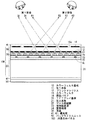
<実施の形態1>
図1および図2は、本発明の実施の形態1に係る2画面表示装置である液晶表示装置の構成を示す図である。図1は当該2画面表示装置の断面図であり、図2はその液晶表示パネル100の平面図である。ここでは、2画面表示装置の例として、複数の観察者が同時に異なる画像を見ることを可能とするデュアルビュー液晶表示装置を示している。
<
1 and 2 are diagrams showing a configuration of a liquid crystal display device which is a two-screen display device according to
図1に示すように、本実施の形態の2画面表示装置は、液晶表示パネル100とその前面側(視認側)および背面側にそれぞれ設けられた偏光板41,42が、バックライトユニット50の前面側に配設された構成となっている。さらに、液晶表示パネル100は、前面側のカラーフィルタ基板10と背面側のTFTアレイ基板20との間に、液晶30が挟持された構成となっている。
As shown in FIG. 1, the two-screen display device according to the present embodiment includes a liquid
カラーフィルタ基板10は、ガラス基板など透明性の第1基板11と、第1基板11の背面側の面(TFTアレイ基板20との対向面)に形成されたブラックマトリクス12およびカラーフィルタ13と、第1基板11の前面側の面に形成された視差バリア14とを備えている。ブラックマトリクス12は、サブ画素間を遮光する遮光膜であり、各サブ画素の領域を規定する開口を有している。カラーフィルタ13は、各サブ画素が発する光(ブラックマトリクス12の開口を通過した光)の色を規定する、赤(R)・緑(G)・青(B)のいずれかの色材である。視差バリア14は、ブラックマトリクス12の開口を通過した光を特定の方向のみに通過する遮光膜であり、金属または黒色の樹脂により形成される。
The
一方、TFTアレイ基板20は、ガラス基板など透明性の第2基板21と、各サブ画素の画素電極24、それら画素電極24に画像信号を供給するための薄膜トランジスタ(Thin Film Transistor;TFT)25、各TFT25のゲート電極に駆動信号を供給するためのゲート線(走査信号線)GL、TFT25のソース電極に画像信号を供給するソース線(画像信号線)SLなどが配設されて成っている。
On the other hand, the
ゲート線GLおよびTFT25のゲート電極は、第2基板21の上面に形成される(図1では不図示)。ゲート線GLおよびTFT25のゲート電極は、ゲート絶縁膜22によって覆われ、当該ゲート絶縁膜22上に、ソース線SLならびにTFT25のソース電極およびドレイン電極が形成される。さらに、ソース線SLおよびTFT25の上は、層間絶縁膜23によって覆われ、当該層間絶縁膜23上に、画素電極24が形成される。画素電極24は、層間絶縁膜23に形成されたコンタクトホールを介してTFT25のドレイン電極に接続されている。
The gate line GL and the gate electrode of the
ここで、視差バリア14の構成および機能について具体的に説明する。視差バリア14は、ブラックマトリクス12の開口と平面視でずれた位置に、スリット状の開口14aを有している。視差バリア14とブラックマトリクス12との間には、所定の間隔(ここでは第1基板11の厚みに相当)が設けられる。この構成により、ブラックマトリクス12の開口(サブ画素)から液晶表示パネル100の正面方向へ出射された光は視差バリア14により遮られ、斜め方向へ出射された光のみが視差バリア14の開口14aを通過する。
Here, the configuration and function of the
2画面表示装置では、視差バリア14の1つの開口14aに対し、ブラックマトリクス12の開口(サブ画素)が2つずつ割り当てられる。すなわち図2のように、液晶表示パネル100の正面から見て、各開口14aの左側には第1画像を表示するための第1サブ画素(赤の第1サブ画素R1、緑の第1サブ画素G1、青の第1サブ画素B1のいずれか)が配設され、各開口14aの右側には第2画像を表示するための第2サブ画素(赤の第2サブ画素R2、緑の第2サブ画素G2、青の第2サブ画素B2のいずれか)が配設される。
In the two-screen display device, two openings (sub-pixels) of the
その結果、図1に示すように、液晶表示パネル100の正面よりも右側からは、視差バリア14の開口14aを通して第1サブ画素R1,G1,B1が表示する第1画像が見え、正面よりも左側からは第2サブ画素R2,G2,B2が表示する第2画像が見えることになる。
As a result, as shown in FIG. 1, the first image displayed by the first sub-pixels R1, G1, and B1 can be seen from the right side of the front surface of the liquid
本実施の形態では、図1のように、視差バリア14とブラックマトリクス12とが、第1基板11の互いに反対側の面に配設されるため、第1基板11は、その厚みにより視差バリア14とブラックマトリクス12との間隔を規定するギャップ層として機能する。通常、第1画像が見える範囲(液晶表示パネル100正面方向に対する角度)と第2画像が見える範囲との差は、ギャップ層を薄くすると大きくなり、ギャップ層を厚くすると小さくなる。よって、異なる観察者に対して異なる画像を表示するデュアルビュー表示装置では、薄いギャップ層が用いられ、一人の観察者の左右の目に異なる画像を視認させる3D表示装置では、厚いギャップ層が用いられる。
In the present embodiment, as shown in FIG. 1, the
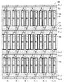
以下、本実施の形態に係る2画面表示装置の液晶表示パネル100の構成の詳細について説明する。液晶表示パネル100の表示領域には、図2のように、第1サブ画素(赤の第1サブ画素R1、緑の第1サブ画素G1および青の第1サブ画素B1のいずれか)と、第2サブ画素(赤の第2サブ画素R2、緑の第2サブ画素G2および青の第2サブ画素B2のいずれか)とが、横方向(ゲート線GLの延在方向)に交互に配設される。
Hereinafter, details of the configuration of the liquid
1つの画素(カラー画素)は、横方向に並ぶ赤、青、緑の3つのサブ画素から構成される。そのため1画面表示装置では、各サブ画素の縦横比は約3:1に設定される。 One pixel (color pixel) is composed of three sub-pixels of red, blue, and green arranged in the horizontal direction. Therefore, in the single screen display device, the aspect ratio of each sub-pixel is set to about 3: 1.
一方、従来の2画面表示装置は、1画面表示装置と同じ構造の表示パネル上に視差バリアを配設した構造を有していたため、各サブ画素の縦横比は1画面表示装置と同様に約3:1であった。そして、その半数が第1画像を表示する第1サブ画素として用いられ、残りの半数が第2画像を表示する第2サブ画素として用いられる。従って、従来の2画面表示装置では、第1画像および第2画像の横方向の解像度が、1画面表示装置の表示画像の半分になっていた。 On the other hand, since the conventional two-screen display device has a structure in which a parallax barrier is provided on a display panel having the same structure as the one-screen display device, the aspect ratio of each sub-pixel is approximately the same as that of the one-screen display device. It was 3: 1. And half of them are used as first sub-pixels for displaying the first image, and the other half are used as second sub-pixels for displaying the second image. Therefore, in the conventional two-screen display device, the horizontal resolution of the first image and the second image is half that of the display image of the single-screen display device.
それに対し、本実施の形態に係る2画面表示装置の液晶表示パネル100では、第1サブ画素および第2サブ画素の横幅を1画面表示装置の半分にし、且つ、第1サブ画素および第2サブ画素を横方向に従来の半分のピッチで配設する。つまり第1サブ画素および第2サブ画素それぞれの縦横比は約6:1であり、横方向に並ぶサブ画素数は従来の2画面表示装置の2倍である。従って、当該液晶表示パネル100における横方向の解像度は、従来の2画面表示装置の2倍、つまり1画面表示装置と同様の解像度となる。
On the other hand, in the liquid
液晶表示パネル100の表示領域には、横方向に隣り合う第1サブ画素および第2サブ画素から成る組が、行列状に複数配設される。以下では、サブ画素の横方向の並びを「行」、縦方向の並びを「列」と称する。また、各サブ画素の縦横比については、本明細書中においては、各サブ画素の領域を規定するブラックマトリクス12の開口部の縦横比を意味するのではなく、行方向、列方向にそれぞれ配列する各サブ画素の繰り返し単位についての縦横比を意味し、配列する各サブ画素の縦方向、横方向、それぞれにおけるピッチの比に相当することになる。
In the display area of the liquid
本実施の形態では、図2のように縦方向(ソース線SLの延在方向)にも第1サブ画素と第2サブ画素とが交互に並ぶように配設される。つまり隣り合うサブ画素行では、第1サブ画素と第2サブ画素との位置関係が逆になる。従って、本実施の形態に係る液晶表示パネル100の表示領域には、縦方向にも横方向にも、第1サブ画素および第2サブ画素が交互に並ぶことになる。言い換えれば、第1サブ画素および第2サブ画素は千鳥状に配設される。
In the present embodiment, the first sub-pixels and the second sub-pixels are arranged alternately in the vertical direction (extending direction of the source line SL) as shown in FIG. That is, in the adjacent sub pixel rows, the positional relationship between the first sub pixel and the second sub pixel is reversed. Therefore, the first subpixel and the second subpixel are alternately arranged in the vertical direction and the horizontal direction in the display area of the liquid
また、視差バリア14の各開口14aは、その左側に第1サブ画素が配置され、右側に第2サブ画素が配置されるようにする必要があるので、図2の如く、開口14aも千鳥状に配設される。
Further, since each
第1サブ画素および第2サブ画素のそれぞれは、赤、緑、青のいずれかの色を発するが、本実施の形態では、第1サブ画素および第2サブ画素のそれぞれが発する色が、横方向に、1つのサブ画素ごとに規則的に変わるように配列される。図2の例では、赤の第1サブ画素R1、緑の第2サブ画素G2、青の第1サブ画素B1、赤の第2サブ画素R2、緑の第1サブ画素G1、青の第2サブ画素B2、赤の第1サブ画素R1…の順に周期的に配列されている。 Each of the first sub-pixel and the second sub-pixel emits one of red, green, and blue. In the present embodiment, the color emitted from each of the first sub-pixel and the second sub-pixel is horizontal. In the direction, the sub-pixels are arranged so as to change regularly. In the example of FIG. 2, the first red subpixel R1, the second green subpixel G2, the first blue subpixel B1, the second red subpixel R2, the first green subpixel G1, the second blue subpixel. The sub-pixels B2 and the red first sub-pixels R1,.
液晶表示パネル100を正面よりも右から見ると、視差バリア14により第2サブ画素が遮られるため、赤の第1サブ画素R1、青の第1サブ画素B1および緑の第1サブ画素G1が横方向に並んで見え、それら3つのサブ画素で1つの画素(カラー画素)が構成される。その結果、液晶表示パネル100の正面よりも右からは、第1画像が見えるようになる。
When the liquid
逆に、液晶表示パネル100を正面よりも左から見ると、視差バリア14により第1サブ画素が遮られるため、緑の第2サブ画素G2、赤の第2サブ画素R2および青の第2サブ画素B2が横方向に並んで見え、それら3つのサブ画素で1つの画素が構成される。その結果、液晶表示パネル100の正面よりも左からは、第2画像が見えるようになる。
Conversely, when the liquid
従って、本実施の形態に係る2画面表示装置の液晶表示パネル100では、横方向に1列に並んで配設される6つのサブ画素、即ち、赤の第1サブ画素R1、青の第1サブ画素B1および緑の第1サブ画素G1、並びに緑の第2サブ画素G2、赤の第2サブ画素R2および青の第2サブ画素B2により、液晶表示パネル100の正面よりも右から観察される第1画像および左から観察される第2画像を併せた1つの画素に対応する基本単位(第1画像および第2画像をそれぞれ表示する赤、緑、青のカラー画素よりなる6つのサブ画素)は構成される。但し、この基本単位を構成する6つのサブ画素における第1画像および第2画像と赤、緑、青の組み合わせ配列は、1行ごとに第1画像および第2画像に対応するサブ画素が入れ替わり2種類の配列を交互に繰り返す形となる。また、この基本単位が行方向、列方向に配列される数により、それぞれ横方向、縦方向の解像度が決定される。なお、第1画像および第2画像について共通の画像を表示させることで、本実施の形態に係る2画面表示装置の液晶表示パネル100は1画面表示装置として活用することも可能であり、その際には、この6つのサブ画素よりなる基本単位が1画面表示装置における1つの画素(カラー画素)に対応する。
Therefore, in the liquid
図2のように、ソース線SLは縦方向に延在し、横方向に隣り合う第1サブ画素と第2サブ画素の間の領域に配設される。各ソース線SLは、それを挟んで隣接する第1サブ画素と第2サブ画素の両方に画像信号を供給するように構成されている。従って、各ソース線SLには、第1サブ画素に接続するTFT25と、その隣の第2サブ画素に接続するTFT25の両方が接続される。
As shown in FIG. 2, the source line SL extends in the vertical direction and is disposed in a region between the first sub-pixel and the second sub-pixel adjacent in the horizontal direction. Each source line SL is configured to supply an image signal to both the first subpixel and the second subpixel adjacent to each other with the source line SL interposed therebetween. Accordingly, each source line SL is connected to both the
そのため、ソース線SLの数はサブ画素列の数の半数となり、図2のように、ソース線SLはサブ画素の2列おきに配置される。従って、本実施の形態に係る2画面表示装置では、横方向の解像度(サブ画素列の数)従来の2倍となるにも関わらず、ソース線SLの数は従来と同じである。 Therefore, the number of source lines SL is half of the number of subpixel columns, and the source lines SL are arranged every two columns of subpixels as shown in FIG. Therefore, in the two-screen display device according to the present embodiment, the number of source lines SL is the same as that in the past, although the horizontal resolution (the number of subpixel columns) is twice that in the past.
このように、ソース線SLが、サブ画素の2列おきに第1サブ画素と第2サブ画素の間に配置され、且つ、開口14aが千鳥状に配設されるので、表示領域上には、図2に示すように、開口14aがソース線SL上に配設される行と、開口14a上に配設されない行とが交互に並ぶことになる。つまり、サブ画素のある行では、同一のソース線SLから画像信号を受ける第1サブ画素と第2サブ画素との間の領域上に開口14aが配設されるが、その隣の行では、互いに異なるソース線SLから画像信号を受ける第1サブ画素と第2サブ画素との間の領域上に開口14aが配設される。
As described above, the source lines SL are arranged between the first sub-pixel and the second sub-pixel every two columns of sub-pixels, and the
ゲート線GLは、TFT25のゲート電極に駆動信号を供給することで各サブ画素を駆動する。各ゲート線GLは、横方向(すなわちゲート線GLと交差する方向)に延在し、各サブ画素行の間に配設される。本実施の形態では、各サブ画素行は、第1サブ画素を駆動するためのゲート線GL(第1ゲート線)と、第2サブ画素を駆動するためのゲート線GL(第2ゲート線)の2本によって駆動される。図2においては、奇数番目のゲート線GLは、各ソース線SLの左側に配置されたサブ画素に接続したTFT25のゲート電極に接続されており、偶数番目のゲート線GLは、各ソース線SLの右側に配置されたサブ画素に接続したTFT25のゲート電極に接続されている(図2においてjは奇数)。つまり、サブ画素の1行につき2本ずつのゲート線GLが設けられる。よってゲート線GLの数は従来の2画面表示装置の場合の2倍となる。
The gate line GL drives each subpixel by supplying a drive signal to the gate electrode of the
図2に示すように、各サブ画素行は、それに属する第1サブ画素を駆動するゲート線GLと、第2サブ画素を駆動するGLとの間に配設される。言い換えれば、1つのサブ画素行を駆動する2本のゲート線GLは、そのサブ画素行を挟むように配設される。よって、各サブ画素行の間には、ゲート線GLが2本ずつ配設されることになる。 As shown in FIG. 2, each subpixel row is disposed between a gate line GL that drives the first subpixel belonging to the subpixel row and a GL that drives the second subpixel. In other words, the two gate lines GL for driving one subpixel row are arranged so as to sandwich the subpixel row. Therefore, two gate lines GL are disposed between each sub-pixel row.
このように本実施の形態に係る2画面表示装置においては、各サブ画素の横幅を従来の2画面表示装置の場合の半分にして縦横比を約6:1とし、且つ、横方向に配置するサブ画素数を従来の2倍とした。それにより、表示領域の寸法を維持したまま、横方向の解像度を従来の倍、すなわち1画面表示装置と同等にすることができる。 As described above, in the two-screen display device according to the present embodiment, the width of each sub-pixel is half that of the conventional two-screen display device, the aspect ratio is about 6: 1, and the sub-pixels are arranged in the horizontal direction. The number of subpixels was doubled. As a result, the horizontal resolution can be made equal to that of the conventional one, that is, the one-screen display device while maintaining the size of the display area.
さらに、第1画像および第2画像を、1画面表示装置の場合と同じ解像度で表示することができる。例えば、従来の2画面表示装置では、1画面表示装置でVGA(640×480)で表示される画像が1/2VGA(320×480)で表示されるが、本実施の形態の2画面表示装置ではそのままVGAの画像として表示できる。 Furthermore, the first image and the second image can be displayed at the same resolution as in the case of the single screen display device. For example, in the conventional two-screen display device, an image displayed in VGA (640 × 480) on the one-screen display device is displayed in 1/2 VGA (320 × 480). Then, it can be displayed as a VGA image as it is.
なお、本実施の形態に係る2画面表示装置の液晶表示パネル100では、横方向に一列に並んで配設される6つのサブ画素により、左右それぞれより観察される赤、緑、青のサブ画素に対応する6つのサブ画素を構成していることから、各サブ画素の縦横比を約6:1とすることで、赤、緑、青の3つのサブ画素で構成される1つの画素は、縦横比が約1:1のほぼ方形に構成される。言い換えると赤、緑、青の3つのサブ画素で構成される画素の縦横に配列するピッチの比が約1:1に構成される。従って、一般的に縦横比が約1:1のほぼ方形に構成される画素を備えた表示装置による表示を想定して作られる映像情報について、想定されるアスペクト比の映像として表示することができる。なお、表示される映像情報のアスペクト比に対して多少の歪みを許容することができる用途などの場合には、各サブ画素の縦横比を約6:1に設定することは必須ではない。
In liquid
また、1本のソース線SLから、2列のサブ画素に画像信号を供給する構成となるため、横方向の解像度が従来の倍になっても、ソース線SLの数は従来と同じである。そのため、画像信号の出力回路(IC)の数は、従来の2画面表示装置の場合と同じでよい。 In addition, since an image signal is supplied from one source line SL to two columns of sub-pixels, the number of source lines SL is the same as before even when the horizontal resolution is doubled. . Therefore, the number of image signal output circuits (ICs) may be the same as that of a conventional two-screen display device.
一方、各サブ画素行において、第1サブ画素と第2サブ画素とを別々のゲート線GLを用いて駆動させる構成となるため、ゲート線GLの数は従来の2倍となる。各画素が赤、緑、青のサブ画素で構成する表示装置では、各画素を1本のゲート配線と3本のソース配線を用いて駆動する。従って、横方向の解像度を倍にする場合、ゲート配線の数を変えずにソース配線数を倍にするよりも、本実施の形態のようにゲート配線を倍にしてソース配線の数を変えない方が、必要な配線の数は少なくて済み、液晶表示パネル100を比較的低コストで作成することができる。
On the other hand, in each sub-pixel row, the first sub-pixel and the second sub-pixel are driven using different gate lines GL, so the number of gate lines GL is twice that of the conventional one. In a display device in which each pixel is composed of red, green, and blue sub-pixels, each pixel is driven using one gate wiring and three source wirings. Therefore, when the horizontal resolution is doubled, the number of source lines is not changed by doubling the gate lines as in this embodiment, rather than doubling the number of source lines without changing the number of gate lines. However, the number of necessary wirings is small, and the liquid
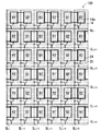
<実施の形態2>
図3および図4は、本発明の実施の形態2に係る2画面表示装置としての液晶表示装置の構成を示す図である。図3は2画面表示装置の断面図であり、図4はその液晶表示パネル100の平面図である。
<
3 and 4 are diagrams showing a configuration of a liquid crystal display device as a two-screen display device according to
実施の形態1では、第1サブ画素および第2サブ画素のそれぞれが発する色を、横方向に、1つのサブ画素ごとに変わるように配列させたが、本実施の形態では、2つのサブ画素ごとに規則的に変わるように配列させている。具体的には、同一のソース線SLから画像信号を受ける第1サブ画素および第2サブ画素を同じ色にしている。その他の構成は、実施の形態1と同様である。
In
図4の例では、各行において、赤の第1サブ画素R1、赤の第2サブ画素R2、緑の第1サブ画素G1、緑の第2サブ画素G2、青の第1サブ画素B1、青の第2サブ画素B2、赤の第1サブ画素R1…の順に周期的に配列されている。 In the example of FIG. 4, in each row, the red first sub-pixel R1, the red second sub-pixel R2, the green first sub-pixel G1, the green second sub-pixel G2, the blue first sub-pixel B1, the blue Of the second sub-pixels B2 and the red first sub-pixels R1,...
図3に示すように、液晶表示パネル100を正面よりも右から見ると、視差バリア14により第2サブ画素が遮られるため、赤の第1サブ画素R1、青の第1サブ画素B1および緑の第1サブ画素G1が横方向に並んで見え、それら3つのサブ画素で1つの画素(カラー画素)が構成される。よってこの場合も、液晶表示パネル100の正面よりも右からは、第1画像が見える。
As shown in FIG. 3, when the liquid
また、液晶表示パネル100を正面よりも左から見ると、視差バリア14により第1サブ画素が遮られるため、緑の第2サブ画素G2、赤の第2サブ画素R2、および青の第2サブ画素B2が横方向に並んで見え、それら3つのサブ画素で1つの画素が構成される。よって、液晶表示パネル100の正面よりも左からは、第2画像が見える。
Further, when the liquid
本実施の形態でも、実施の形態1と同様の効果が得られる。 In the present embodiment, the same effect as in the first embodiment can be obtained.
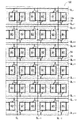
<実施の形態3>
図5は、本発明の実施の形態3に係る2画面表示装置としての液晶表示装置の構成を示す図であり、当該2画面表示装置が備える液晶表示パネル100の平面図である。
<
FIG. 5 is a diagram showing a configuration of a liquid crystal display device as a two-screen display device according to
実施の形態3では、視差バリア14の開口14aを、千鳥状でなく、行列状に配設している。具体的には、表示領域上の全ての開口14aを、ソース線SL上に設けている。すなわち、全ての開口14aは、同一のソース線SLから画像信号を受ける第1サブ画素と第2サブ画素との間の領域上に配設される。
In the third embodiment, the
その他の構成は、実施の形態2とほぼ同様であるが、開口14aが行列状に配設される結果、表示領域には、第1サブ画素のみから成る列と、第2サブ画素のみから成る列とが交互に並ぶことになる。各サブ画素行で、第1サブ画素と第2サブ画素との位置関係は全て同じになる。
Other configurations are almost the same as those of the second embodiment. As a result of the
本実施の形態でも、実施の形態1と同様の効果が得られる。 In the present embodiment, the same effect as in the first embodiment can be obtained.
<実施の形態4>
実施の形態4では、本発明に係る2画面表示装置に適した駆動方法を説明する。
<
In
まず、それに先立って、従来の2画面表示装置の駆動に関しての問題を説明する。一般に、液晶表示装置では、液晶を交流で駆動させることに起因するフリッカ(画像のちらつき)の発生を抑制する目的で、ドット反転駆動やその派生系による液晶の駆動方法が採用されることが多い。ドット反転駆動方式は、ソース線に供給する画像信号の極性をゲート線ごとに反転させ、且つ、隣り合うソース線の画像信号を互いに逆極性にするものである。 Prior to that, problems relating to driving of a conventional two-screen display device will be described. In general, in a liquid crystal display device, in order to suppress the occurrence of flicker (image flicker) caused by driving a liquid crystal with alternating current, a dot inversion driving method or a liquid crystal driving method using a derivative system is often employed. . In the dot inversion driving method, the polarity of an image signal supplied to a source line is inverted for each gate line, and the image signals of adjacent source lines are reversed to each other.
図14は、従来の2画面表示装置をドット反転駆動させた場合における、各サブ画素に供給される画像信号の極性(以下、単に「サブ画素の極性」と称することもある)の正(+)/負(−)を示す図である。従来の2画面表示装置では、各サブ画素列はそれぞれ個別のソース線SLから画像信号を受け、各サブ画素行はそれぞれ個別のゲート線GLで駆動されるので、画像信号の極性は、縦方向(列方向)および横方向(行方向)の両方で、1つのサブ画素ごとに反転する。 FIG. 14 shows a positive (+) polarity of an image signal supplied to each sub-pixel (hereinafter sometimes simply referred to as “sub-pixel polarity”) when a conventional two-screen display device is driven by dot inversion. It is a figure which shows negative / (-). In the conventional two-screen display device, each sub pixel column receives an image signal from an individual source line SL, and each sub pixel row is driven by an individual gate line GL. Inversion is performed for each sub-pixel both in the (column direction) and in the horizontal direction (row direction).
あるフレームにおいて、例えば図14のように、第i番目のソース線SLiから画像信号を受けるサブ画素列で、第j番目のゲート線GLjで駆動されるサブ画素から順に、画像信号の極性を+、−、+、−、+、…と変化させるとする。この場合、第i+1番目のソース線SLi+1から画像信号を受けるサブ画素列では、第j番目のゲート線GLjで駆動されるサブ画素から順に、画像信号の極性を−、+、−、+、−、…と変化させる。同様に、ソース線SLi+2では、画像信号の極性をゲート線GLjから順に+、−、+、−、+、…と変化させ、ソース線SLi+3では、画像信号の極性をゲート線GLjから順に−、+、−、+、−、…と変化させる。なお、各サブ画素の極性は、フレームごとに反転するため、次のフレームでは、各サブ画素の極性は図14の状態の逆になる。 In a certain frame, for example, as shown in FIG. 14, the polarity of the image signal in the sub-pixel column that receives the image signal from the i-th source line SL i and sequentially from the sub-pixel driven by the j-th gate line GL j. Are changed to +, −, +, −, +,. In this case, in the sub pixel column that receives the image signal from the (i + 1) th source line SL i + 1 , the polarity of the image signal is set to −, +, − in order from the sub pixel driven by the jth gate line GL j. , +,-, And so on. Similarly, in the source line SL i + 2 , the polarity of the image signal is changed sequentially from the gate line GL j to +, −, +, −, +,..., And in the source line SL i + 3 , the polarity of the image signal is changed. In order from the gate line GL j , −, +, −, +, −,. Since the polarity of each sub-pixel is inverted every frame, in the next frame, the polarity of each sub-pixel is the reverse of the state shown in FIG.
1画面表示装置では、このようにサブ画素の極性を互い違いにすることで、フリッカの発生が抑えられる効果が得られる。しかし、図14に示すような従来の2画面表示装置では、その効果を充分に得ることができない。 In the one-screen display device, the effect of suppressing the occurrence of flicker can be obtained by alternating the polarities of the sub-pixels in this way. However, the conventional two-screen display device as shown in FIG. 14 cannot sufficiently obtain the effect.
図14の例では、第1サブ画素(赤の第1サブ画素R1、緑の第1サブ画素G1、青の第1サブ画素B1)の全てが正極性(+)であり、第2サブ画素(赤の第2サブ画素R2、緑の第2サブ画素G2、青の第2サブ画素B2)の全てが負極性(−)となっている。従って、第1画像は正極性のサブ画素のみで表示され、第2画素は負極性のサブ画素のみで表示される。また次のフレームでは、第1画像は負極性のサブ画素のみで表示され、第2画素は正極性のサブ画素のみで表示される。つまり、第1画像および第2画像は、各フレームで同一極性のサブ画素のみで表示される。その場合、駆動信号に僅かなずれが生じてもフリッカが発生する。 In the example of FIG. 14, all of the first sub-pixels (the red first sub-pixel R1, the green first sub-pixel G1, the blue first sub-pixel B1) are positive (+), and the second sub-pixel All of (the red second sub-pixel R2, the green second sub-pixel G2, the blue second sub-pixel B2) are negative (-). Accordingly, the first image is displayed with only positive sub-pixels, and the second pixel is displayed with only negative sub-pixels. In the next frame, the first image is displayed with only negative sub-pixels, and the second pixel is displayed with only positive sub-pixels. That is, the first image and the second image are displayed only with sub-pixels having the same polarity in each frame. In that case, flicker occurs even if a slight shift occurs in the drive signal.
図14と同じ構成の2画面表示装置で、フリッカの発生を抑える方法として「1×2駆動方式」と呼ばれるものがある。1×2駆動方式では、ソース線に供給する画像信号の極性をゲート線の2本ごとに反転させ、且つ、隣り合うソース線の画像信号を互いに逆極性にするものである。 There is a so-called “1 × 2 drive method” as a method of suppressing the occurrence of flicker in the two-screen display device having the same configuration as FIG. In the 1 × 2 driving method, the polarity of an image signal supplied to a source line is inverted every two gate lines, and the image signals of adjacent source lines are reversed to each other.
図15は、従来の2画面表示装置を1×2駆動させた場合における、各サブ画素に供給される画像信号の極性(サブ画素の極性)を示す図である。あるフレームにおいて、例えば図15のように、第i番目のソース線SLiから画像信号を受けるサブ画素列で、第j番目のゲート線GLjで駆動されるサブ画素から順に、画像信号の極性を+、+、−、−、−、+、+、…と2本のゲート線GLのごとに変化させるとする。この場合、第i+1番目のソース線SLi+1から画像信号を受けるサブ画素列では、第j番目のゲート線GLjで駆動されるサブ画素から順に、画像信号の極性を−、−、+、+、−、−、…と変化させる。同様に、ソース線SLi+2では、画像信号の極性をゲート線GLjから順に+、+、−、−、−、+、+、…と変化させ、ソース線SLi+3では、画像信号の極性をゲート線GLjから順に−、−、+、+、−、−、…と変化させる。なお、1×2駆動でも、各サブ画素の極性はフレームごとに反転する。 FIG. 15 is a diagram showing the polarity of the image signal supplied to each sub-pixel (sub-pixel polarity) when the conventional two-screen display device is driven 1 × 2. In a certain frame, for example, as shown in FIG. 15, the polarity of the image signal in order from the sub-pixel driven by the j-th gate line GL j in the sub-pixel column that receives the image signal from the i-th source line SL i. Are changed for each of the two gate lines GL, +, +, −, −, −, +, +,. In this case, in the subpixel column that receives the image signal from the (i + 1) th source line SL i + 1 , the polarity of the image signal is set to −, −, + in order from the subpixel driven by the jth gate line GLj. , +,-,-, ... Similarly, the source line SL i + 2, +, +, in order from the gate line GL j the polarity of the image signal -, -, -, +, +, ... and varied, the source line SL i + 3, image The signal polarity is changed in order from the gate line GL j to-,-, +, +,-,-,. Even in 1 × 2 driving, the polarity of each sub-pixel is inverted every frame.
1×2駆動の場合、第1画像および第2画像が同一極性のサブ画素のみで表示されることは回避できる。しかし、各サブ画素行では、第1サブ画素は全て同じ極性になり、第2サブ画素も全て同じ極性となる。例えば図15のように、ゲート線GLjで駆動されるサブ画素行では、第1サブ画素は全て正極性、第2サブ画素は全て負極性となる。ゲート線GLj+1で駆動されるサブ画素行と、ゲート線GLj+2で駆動されるサブ画素行では、第1サブ画素は全て負極性、第2サブ画素は全て正極性となる。さらに、ゲート線GLj+3で駆動されるサブ画素行と、ゲート線GLj+4で駆動されるサブ画素行では、第1サブ画素は全て正極性、第2サブ画素は全て負極性となる。 In the case of 1 × 2 driving, it can be avoided that the first image and the second image are displayed only by sub-pixels having the same polarity. However, in each subpixel row, the first subpixels all have the same polarity, and the second subpixels all have the same polarity. For example, as shown in FIG. 15, in the sub-pixel row driven by the gate line GL j , the first sub-pixels are all positive and the second sub-pixels are all negative. In the sub-pixel row driven by the gate line GL j + 1 and the sub-pixel row driven by the gate line GL j + 2 , the first sub-pixels are all negative and the second sub-pixels are all positive. Further, in the sub-pixel row driven by the gate line GL j + 3 and the sub-pixel row driven by the gate line GL j + 4 , the first sub-pixels are all positive and the second sub-pixels are all negative. Become.
よって、1×2駆動の場合には、第1画像および第2画像のそれぞれにおいて、正極性のみのサブ画素行と、負極性のみのサブ画素行とが、2行ごとに繰り返されることになる。このように、第1画像よび第2画像が、連続して直線状に並ぶ同一極性のサブ画素群を含む場合、その部分に直線状の輝度ムラ(すなわち明暗の線)が現れやすく、画質を低下させる原因となる。 Therefore, in the case of 1 × 2 driving, in each of the first image and the second image, the sub-pixel row having only positive polarity and the sub-pixel row having only negative polarity are repeated every two rows. . As described above, when the first image and the second image include sub-pixel groups having the same polarity arranged in a straight line, linear luminance unevenness (that is, light and dark lines) is likely to appear in the portion, and the image quality is improved. It causes a decrease.
実施の形態1,2に示した2画面表示装置(図2,図4)では、上記の問題は生じない。すなわち、ドット反転駆動や1×2駆動により、フリッカおよび輝度ムラを抑制することができる。そのことを図6および図7を用いて説明する。 In the two-screen display devices (FIGS. 2 and 4) shown in the first and second embodiments, the above problem does not occur. That is, flicker and luminance unevenness can be suppressed by dot inversion driving and 1 × 2 driving. This will be described with reference to FIGS.
図6は、図2に示した2画面表示装置をドット反転駆動させた場合における、各サブ画素に供給される画像信号の極性を示す図である。図2の2画面表示装置では、1本のソース線SLが2列のサブ画素に画像信号を供給し、各サブ画素行は2本のゲート線GLにより駆動される(第1サブ画素と第2サブ画素とが異なるゲート線GLで駆動される)。そのため、図14の場合と同様に、ソース線SLに供給する画像信号の極性をゲート線GLごとに反転させ、且つ、隣り合うソース線SLの画像信号を互いに逆極性にすると、図6のように、各行のサブ画素の極性は、横方向に+、+、−、−、+、+、…と変化する。 FIG. 6 is a diagram showing the polarities of image signals supplied to the sub-pixels when the two-screen display device shown in FIG. 2 is driven by dot inversion. In the two-screen display device of FIG. 2, one source line SL supplies image signals to two columns of subpixels, and each subpixel row is driven by two gate lines GL (the first subpixel and the first subpixel). The two sub-pixels are driven by different gate lines GL). Therefore, as in the case of FIG. 14, when the polarity of the image signal supplied to the source line SL is inverted for each gate line GL and the image signals of the adjacent source lines SL are opposite to each other, as shown in FIG. In addition, the polarities of the sub-pixels in each row change in the horizontal direction as +, +, −, −, +, +,.
従って、第1サブ画素(赤の第1サブ画素R1、緑の第1サブ画素G1、青の第1サブ画素B1)および第2サブ画素(赤の第2サブ画素R2、緑の第2サブ画素G2、青の第2サブ画素B2)がそれぞれ同一極性のみになることはなく、フリッカの発生を抑制できる。また、連続して直線状に並ぶ同一極性のサブ画素群も構成されないので、直線状の輝度ムラの発生も防止される。 Accordingly, the first sub-pixel (the red first sub-pixel R1, the green first sub-pixel G1, the blue first sub-pixel B1) and the second sub-pixel (the red second sub-pixel R2, the green second sub-pixel). The pixel G2 and the blue second sub-pixel B2) do not have the same polarity, and the occurrence of flicker can be suppressed. In addition, since the sub-pixel groups having the same polarity arranged continuously in a straight line are not configured, the occurrence of linear luminance unevenness is also prevented.
また、図7は、図2に示した2画面表示装置を1×2駆動させた場合における、各サブ画素に供給される画像信号の極性を示す図である。図2の2画面表示装置に対し、図15の場合と同様に、ソース線SLに供給する画像信号の極性を2本のゲート線GLごとに(一組の第1ゲート線および第2ゲート線ごとに)反転させ、且つ、隣り合うソース線SLの画像信号を互いに逆極性にすると、図7のように、この場合も各行のサブ画素の極性は、横方向に+、+、−、−、+、+、…と変化する。 FIG. 7 is a diagram showing the polarities of the image signals supplied to the sub-pixels when the two-screen display device shown in FIG. 2 is driven 1 × 2. 2, the polarity of the image signal supplied to the source line SL is set for each of the two gate lines GL (a set of the first gate line and the second gate line) as in the case of FIG. When the image signals of the adjacent source lines SL are reversed to each other, as shown in FIG. 7, the polarities of the sub-pixels in each row are also +, +, −, − in the horizontal direction. , +, +, And so on.
従って、第1サブ画素および第2サブ画素がそれぞれ同一極性のみになることはなく、フリッカの発生を抑制できる。また、連続して直線状に並ぶ同一極性のサブ画素群も構成されないので、直線状の輝度ムラの発生も防止される。 Therefore, the first subpixel and the second subpixel do not have only the same polarity, and the occurrence of flicker can be suppressed. In addition, since the sub-pixel groups having the same polarity arranged continuously in a straight line are not configured, the occurrence of linear luminance unevenness is also prevented.
<実施の形態5>
図8は、実施の形態5に係る2画面表示装置の液晶表示パネル100の平面図である。当該液晶表示パネル100の回路構成は、図14に示した従来の2画面表示装置に類似しているが、第1サブ画素および第2サブ画素の縦の長さを1画面表示装置の半分にし、且つ、サブ画素を縦方向に従来の半分のピッチで配設している。つまり第1サブ画素および第2サブ画素それぞれの縦横比は約3:2であり、縦方向に並ぶサブ画素数は従来の2画面表示装置の2倍である。
<
FIG. 8 is a plan view of the liquid
本実施の形態では、1つの画素(カラー画素)は、2行のサブ画素に跨るように構成される。図9は、実施の形態5に係る2画面表示装置の液晶表示パネル100における画素とそれを構成するサブ画素との関係を示す図である。第1画像を表示する画素(第1画像用画素)は、図9に点線で示す3角形の頂点に位置する3つの第1サブ画素(赤の第1サブ画素R1、緑の第1サブ画素G1、青の第1サブ画素B1)により構成される。また第2画像を表示する画素(第2画像用画素)は、同図において一点鎖線で示す3角形の頂点に位置する3つの第1サブ画素(赤の第2サブ画素R2、緑の第2サブ画素G2、青の第2サブ画素B2)により構成される。従って、第1画像および第2画像をそれぞれ表示する赤、緑、青のカラー画素よりなる基本単位としては、横方向に3列、縦方向に2行よりなる6つのサブ画素により構成される。
In the present embodiment, one pixel (color pixel) is configured to straddle two rows of sub-pixels. FIG. 9 is a diagram illustrating a relationship between pixels in the liquid
従来の2画面表示装置における1つの画素は、縦の長さがサブ画素の1行分に相当し、横幅がサブ画素の6列分に相当していた。それに対し、本実施の形態の2画面表示装置における1つの画素は、図9の如く、縦の長さがサブ画素の2行分に相当し、横幅がサブ画素の3列分に相当する。但し、本実施の形態のサブ画素の縦の長さは、従来の半分である。従って、本実施の形態の2画面表示装置の画素は、従来の2画面表示装置の画素に対し、縦の長さが同じで横幅が半分となる。その結果、本実施の形態の2画面表示装置における横方向の解像度は、従来の2画面表示装置の2倍、つまり1画面表示装置と同様の解像度となる。 One pixel in the conventional two-screen display device has a vertical length corresponding to one row of subpixels, and a horizontal width corresponding to six columns of subpixels. On the other hand, as shown in FIG. 9, one pixel in the two-screen display device of this embodiment has a vertical length corresponding to two rows of subpixels and a horizontal width corresponding to three columns of subpixels. However, the vertical length of the sub-pixel in this embodiment is half of the conventional length. Therefore, the pixels of the two-screen display device of this embodiment have the same vertical length and half the horizontal width as compared with the pixels of the conventional two-screen display device. As a result, the horizontal resolution in the two-screen display device of the present embodiment is twice that of the conventional two-screen display device, that is, the same resolution as that of the single-screen display device.
液晶表示パネル100の表示領域には、横方向に隣り合う第1サブ画素および第2サブ画素から成る組が、行列状に複数配設される。本実施の形態では、図8のように縦方向(ソース線SLの延在方向)にも第1サブ画素と第2サブ画素とが交互に並ぶように配設される。つまり隣り合うサブ画素行では、第1サブ画素と第2サブ画素との位置関係が逆になる。よって、視差バリア14の開口14aは千鳥状に配設される。また、サブ画素が縦方向に従来の半分のピッチで配設されているため、開口14aの縦方向のピッチも従来の半分となる。
In the display area of the liquid
第1サブ画素および第2サブ画素のそれぞれは、赤、緑、青のいずれかの色を発するが、本実施の形態では、第1サブ画素および第2サブ画素のそれぞれが発する色が、横方向に、1つのサブ画素ごとに規則的に変わるように配列される。図8の例では、赤の第1サブ画素R1、緑の第2サブ画素G2、青の第1サブ画素B1、赤の第2サブ画素R2、緑の第1サブ画素G1、青の第2サブ画素B2、赤の第1サブ画素R1…の順に周期的に配列されている。 Each of the first sub-pixel and the second sub-pixel emits one of red, green, and blue. In the present embodiment, the color emitted from each of the first sub-pixel and the second sub-pixel is horizontal. In the direction, the sub-pixels are arranged so as to change regularly. In the example of FIG. 8, the first red subpixel R1, the second green subpixel G2, the first blue subpixel B1, the second red subpixel R2, the first green subpixel G1, the second blue subpixel. The sub-pixels B2 and the red first sub-pixels R1,.
液晶表示パネル100を正面よりも右から見ると、視差バリア14により第2サブ画素が遮られるため、三角形の頂点状に並ぶ赤の第1サブ画素R1、青の第1サブ画素B1および緑の第1サブ画素G1が1つの画素を構成する。その結果、液晶表示パネル100の正面よりも右からは、第1画像が見える。
When the liquid
逆に、液晶表示パネル100を正面よりも左から見ると、視差バリア14により第1サブ画素が遮られるため、三角形の頂点状に並ぶ緑の第2サブ画素G2、赤の第2サブ画素R2および青の第2サブ画素B2が1つの画素を構成する。その結果、液晶表示パネル100の正面よりも左からは、第2画像が見える。
Conversely, when the liquid
ソース線SLは、縦方向に延在し、サブ画素の各列の間の領域に配設される。サブ画素の各列には、それぞれ個別のソース線SLから画像信号が供給される。つまり本実施の形態では、隣接する第1サブ画素と第2サブ画素に、それぞれ個別のソース線SLから画像信号が供給される。よって、ソース線SLの数はサブ画素列の数と同じ、すなわち従来の2画面表示装置の場合と同じである。 The source line SL extends in the vertical direction and is disposed in a region between each column of subpixels. An image signal is supplied from each individual source line SL to each column of sub-pixels. That is, in this embodiment, image signals are supplied from the individual source lines SL to the adjacent first subpixel and second subpixel, respectively. Therefore, the number of source lines SL is the same as the number of subpixel columns, that is, the same as in the case of a conventional two-screen display device.
また、ソース線SLは、サブ画素の各列の間に配設されるので、視差バリア14において千鳥状に配設された開口14aは、いずれもソース線SLの上方に位置することになる。
Further, since the source lines SL are disposed between the columns of the sub-pixels, all the
一方、各ゲート線GLは、横方向に延在し、各サブ画素行の間に配設される。各サブ画素行に対してゲート線GLが1本ずつ設けられ、同じ行のサブ画素はすべて同じゲート線GLによって駆動される。但し、本実施の形態では、サブ画素は、縦の長さが従来の半分であり、縦方向に従来の半分のピッチで配設されているため、ゲート線GLの数は従来の2倍となる。 On the other hand, each gate line GL extends in the horizontal direction and is disposed between the sub-pixel rows. One gate line GL is provided for each subpixel row, and all subpixels in the same row are driven by the same gate line GL. However, in this embodiment, the vertical length of the sub-pixels is half that of the conventional one, and the sub-pixels are arranged in the vertical direction at half the conventional pitch, so the number of gate lines GL is twice that of the conventional one. Become.
このように、本実施の形態に係る2画面表示装置では、各サブ画素の縦の長さを従来の2画面表示装置の場合の半分にして縦横比を約3:2であり、且つ、それぞれの画素(カラー画素)が2行のサブ画素に跨って構成される。それにより、1つの画素の横幅は従来の半分(サブ画素の3行分)になる。よって、表示領域の寸法を維持したまま、横方向の解像度を従来の倍、すなわち1画面表示装置と同等にすることができる。その結果、第1画像および第2画像を、1画面表示装置の場合と同じ解像度で表示することができる。 Thus, in the two-screen display device according to the present embodiment, the vertical length of each sub-pixel is half that of the conventional two-screen display device, the aspect ratio is about 3: 2, and each Pixels (color pixels) are formed across two rows of sub-pixels. As a result, the horizontal width of one pixel is half that of the conventional one (for three rows of sub-pixels). Accordingly, the horizontal resolution can be made equal to that of the conventional one, that is, a single-screen display device while maintaining the size of the display area. As a result, the first image and the second image can be displayed with the same resolution as that of the single-screen display device.
また、本実施の形態の2画面表示装置における各サブ画素の横幅、およびサブ画素の横方向のピッチは、従来の2画面表示装置の場合と同じである。よって、視差バリアと画素との間のギャップは、従来の2画面表示装置と同じでよい。そのため、例えば図1に示した構成のように、視差バリアと画素との間隔(ブラックマトリクス12と視差バリア14との間隔)が第1基板11の厚さによって規定される場合でも、当該第1基板11の厚さは従来と同じでよい。よって、従来の表示装置の製造プロセスを容易に適用でき、製造コストの増大を抑えることができる。
Further, the horizontal width of each sub-pixel and the horizontal pitch of the sub-pixel in the two-screen display device of the present embodiment are the same as those in the conventional two-screen display device. Therefore, the gap between the parallax barrier and the pixel may be the same as that of the conventional two-screen display device. Therefore, even when the interval between the parallax barrier and the pixel (the interval between the
<実施の形態6>
図10は、本発明の実施の形態6に係る2画面表示装置の液晶表示パネル100の平面図である。実施の形態6の液晶表示パネル100は、回路構成が実施の形態5と同じであるが、各要素のレイアウトが実施の形態5とは異なっている。
<
FIG. 10 is a plan view of the liquid
本実施の形態では、ゲート線GLを、各サブ画素行の間に1本ずつ配設するのではなく、サブ画素の2行おきに2本ずつ配設している。また、2本のゲート線GLを挟む2行のサブ画素のそれぞれは、その2本のゲート線GLのうちの近い方によって駆動される。すなわち、図10において、隣り合う2本のゲート線GLj+1,GLj+2のうち、上側のゲート線GLj+1は、その上側に位置するサブ画素行を駆動し、下側のゲート線GLj+2は、その下側に位置するサブ画素行を駆動する。 In this embodiment, one gate line GL is not provided between each sub-pixel row, but two gate lines GL are provided every two sub-pixel rows. Further, each of the two rows of sub-pixels sandwiching the two gate lines GL is driven by the closer one of the two gate lines GL. That is, in FIG. 10, of the two adjacent gate lines GL j + 1 and GL j + 2 , the upper gate line GL j + 1 drives the sub-pixel row located above the lower gate line GL j + 1 . The gate line GL j + 2 drives a sub-pixel row located therebelow.
言い換えれば、隣り合う2行のサブ画素は、その一方を駆動するゲート線GLと、もう一方を駆動するゲート線GLとの間に配設される。すなわち、図10において、ゲート線GLjとゲート線GLj+1との間に配設された2行のサブ画素は、その一方がゲート線GLjにより駆動され、もう一方はゲート線GLj+1により駆動される。 In other words, two adjacent rows of sub-pixels are arranged between a gate line GL that drives one of them and a gate line GL that drives the other. That is, in FIG. 10, the sub-pixels of two rows disposed between the gate line GL j and the gate line GL j + 1, the one of which is driven by the gate line GL j, the other gate lines GL j Driven by +1 .
本実施の形態においても、各画素(カラー画素)は、図9のように2行のサブ画素に跨るように構成される。本実施の形態では、サブ画素を2行ずつ近接させて配設することができるので、1つの画素を構成する3つのサブ画素を互いに近接させて配置できる。 Also in this embodiment, each pixel (color pixel) is configured to straddle two rows of sub-pixels as shown in FIG. In this embodiment mode, the sub-pixels can be arranged close to each other by two rows, so that the three sub-pixels constituting one pixel can be arranged close to each other.
<実施の形態7>
実施の形態7では、実施の形態5(図8)の2画面表示装置に、実施の形態1の回路構成を応用する。図11は、実施の形態7に係る2画面表示装置の液晶表示パネル100の平面図である。
<
In the seventh embodiment, the circuit configuration of the first embodiment is applied to the two-screen display device of the fifth embodiment (FIG. 8). FIG. 11 is a plan view of the liquid
本実施の形態に係る2画面表示装置の液晶表示パネル100では、各サブ画素のサイズおよびレイアウトは実施の形態5と同様である。つまり、各サブ画素それぞれの縦横比は約3:2であり、且つ、サブ画素を縦方向に従来の半分のピッチで配設している。また図9に示したように、1行の画素(カラー画素)は2行のサブ画素を用いて構成される。よって、当該液晶表示パネル100における横方向の解像度は、従来の2画面表示装置の2倍、つまり1画面表示装置と同様の解像度となる。
In the liquid
なお、本実施の形態でも、横方向および縦方向に第1サブ画素と第2サブ画素とが交互に並ぶように配設され、視差バリア14の開口14aは千鳥状に配設される。また、サブ画素が縦方向に従来の半分のピッチで配設されているため、開口14aの縦方向のピッチも従来の半分となる。
Also in this embodiment, the first sub-pixels and the second sub-pixels are arranged alternately in the horizontal direction and the vertical direction, and the
第1サブ画素および第2サブ画素のそれぞれは、赤、緑、青のいずれかの色を発するが、本実施の形態では、第1サブ画素および第2サブ画素のそれぞれが発する色が、横方向に、1つのサブ画素ごとに規則的に変わるように配列される。図11の例では、赤の第1サブ画素R1、緑の第2サブ画素G2、青の第1サブ画素B1、赤の第2サブ画素R2、緑の第1サブ画素G1、青の第2サブ画素B2、赤の第1サブ画素R1…の順に周期的に配列されている。 Each of the first sub-pixel and the second sub-pixel emits one of red, green, and blue. In the present embodiment, the color emitted from each of the first sub-pixel and the second sub-pixel is horizontal. In the direction, the sub-pixels are arranged so as to change regularly. In the example of FIG. 11, the first red subpixel R1, the second green subpixel G2, the first blue subpixel B1, the second red subpixel R2, the first green subpixel G1, the second blue subpixel. The sub-pixels B2 and the red first sub-pixels R1,.
液晶表示パネル100を正面よりも右から見ると、視差バリア14により第2サブ画素が遮られるため、三角形の頂点状に並ぶ赤の第1サブ画素R1、青の第1サブ画素B1および緑の第1サブ画素G1が1つの画素を構成する。その結果、液晶表示パネル100の正面よりも右からは、第1画像が見える。
When the liquid
逆に、液晶表示パネル100を正面よりも左から見ると、視差バリア14により第1サブ画素が遮られるため、三角形の頂点状に並ぶ緑の第2サブ画素G2、赤の第2サブ画素R2および青の第2サブ画素B2が1つの画素を構成する。その結果、液晶表示パネル100の正面よりも左からは、第2画像が見える。
Conversely, when the liquid
図11のように、ソース線SLは、縦方向に延在し、横方向に隣り合う第1サブ画素と第2サブ画素の間の領域に配設される。各ソース線SLは、それを挟んで隣接する第1サブ画素と第2サブ画素の両方に画像信号を供給するように構成されている。従って、各ソース線SLには、第1サブ画素に接続するTFT25と、その隣の第2サブ画素に接続するTFT25の両方が接続される。
As shown in FIG. 11, the source line SL extends in the vertical direction and is disposed in a region between the first subpixel and the second subpixel that are adjacent in the horizontal direction. Each source line SL is configured to supply an image signal to both the first subpixel and the second subpixel adjacent to each other with the source line SL interposed therebetween. Accordingly, each source line SL is connected to both the
そのため、ソース線SLの数はサブ画素列の数の半数でよく、図11のように、ソース線SLはサブ画素の2列おきに配置される。本実施の形態に係る2画面表示装置では、横方向のサブ画素列の数が従来と同じなので、ソース線SLの数は従来の半分でよい。 Therefore, the number of source lines SL may be half of the number of subpixel columns, and the source lines SL are arranged every two columns of subpixels as shown in FIG. In the two-screen display device according to the present embodiment, since the number of horizontal sub-pixel columns is the same as the conventional one, the number of source lines SL may be half that of the conventional one.
このように、ソース線SLが、サブ画素の2列おきに第1サブ画素と第2サブ画素の間に配置され、且つ、開口14aが千鳥状に配設されるので、図11に示すように、開口14aがソース線SL上に配設される行と、開口14a上に配設されない行とが交互に配設されることになる。つまり、サブ画素のある行では、開口14aが同一のソース線SLから画像信号を受ける第1サブ画素と第2サブ画素との間の領域上に配設されるが、その隣の行では、開口14aが、互いに異なるソース線SLから画像信号を受ける第1サブ画素と第2サブ画素との間の領域上に配設される。
As described above, the source lines SL are arranged between the first subpixel and the second subpixel every two columns of subpixels, and the
一方、各ゲート線GLは、横方向に延在し、各サブ画素行の間に配設される。本実施の形態では、各サブ画素行に対して、第1サブ画素を駆動するためのゲート線GL(第1ゲート線)と、第2サブ画素を駆動するためのゲート線GL(第2ゲート線)の2本が設けられる。図11においては、奇数番目のゲート線GLは、各ソース線SLの左側に配置されたサブ画素に接続したTFT25のゲート電極に接続されており、偶数番目のゲート線GLは、各ソース線SLの右側に配置されたサブ画素に接続したTFT25のゲート電極に接続されている(図11においてjは奇数)。
On the other hand, each gate line GL extends in the horizontal direction and is disposed between the sub-pixel rows. In the present embodiment, for each subpixel row, a gate line GL (first gate line) for driving the first subpixel and a gate line GL (second gate) for driving the second subpixel. Two lines) are provided. In FIG. 11, the odd-numbered gate lines GL are connected to the gate electrodes of the
つまり、サブ画素の1行につき2本ずつのゲート線GLが設けられる。また本実施の形態では、サブ画素行の数は従来の2倍である。よってゲート線GLの数は従来の4倍となる。 That is, two gate lines GL are provided for each row of subpixels. In the present embodiment, the number of subpixel rows is twice that of the prior art. Therefore, the number of gate lines GL is four times that of the prior art.
本実施の形態では、各サブ画素行は、その第1サブ画素を駆動するゲート線GLと、第2サブ画素を駆動するGLとの間に配設される。言い換えれば、サブ画素行を駆動する2本のゲート線GLは、それらが駆動するサブ画素行を挟むように配設される。よって、各サブ画素行の間には、図11のようにゲート線GLが2本ずつ配設されることになる。 In the present embodiment, each subpixel row is disposed between a gate line GL that drives the first subpixel and a GL that drives the second subpixel. In other words, the two gate lines GL that drive the sub-pixel rows are arranged so as to sandwich the sub-pixel row that they drive. Therefore, two gate lines GL are provided between each sub-pixel row as shown in FIG.
このように、本実施の形態に係る2画面表示装置では、各サブ画素の縦の長さを従来の2画面表示装置の場合の半分にして縦横比を約3:2であり、且つ、それぞれの画素(カラー画素)がサブ画素の2行に跨って構成される。それにより、1つの画素の横幅を従来の半分(サブ画素の3行分)になる。よって、表示領域の寸法を維持したまま、横方向の解像度を従来の倍、すなわち1画面表示装置と同等にすることができる。その結果、第1画像および第2画像を、1画面表示装置の場合と同じ解像度で表示することができる。 Thus, in the two-screen display device according to the present embodiment, the vertical length of each sub-pixel is half that of the conventional two-screen display device, the aspect ratio is about 3: 2, and each Pixels (color pixels) are formed across two rows of sub-pixels. As a result, the horizontal width of one pixel is half that of the conventional one (3 rows of sub-pixels). Accordingly, the horizontal resolution can be made equal to that of the conventional one, that is, a single-screen display device while maintaining the size of the display area. As a result, the first image and the second image can be displayed with the same resolution as that of the single-screen display device.
また、本実施の形態の2画面表示装置における各サブ画素の横幅およびサブ画素の横方向のピッチは、従来の2画面表示装置の場合と同じである。よって、視差バリアと画素との間のギャップは、従来の2画面表示装置と同じでよい。そのため、例えば図1のように、視差バリアと画素との間隔(ブラックマトリクス12と視差バリア14との間隔)が第1基板11の厚さによって規定される場合でも、当該第1基板11の厚さは従来と同じでよい。よって、従来の表示装置の製造プロセスを容易に適用でき、製造コストの増大を抑えることができる。
Further, the horizontal width of each sub-pixel and the horizontal pitch of the sub-pixel in the two-screen display device of the present embodiment are the same as those in the conventional two-screen display device. Therefore, the gap between the parallax barrier and the pixel may be the same as that of the conventional two-screen display device. Therefore, for example, as shown in FIG. 1, even when the distance between the parallax barrier and the pixel (the distance between the
<実施の形態8>
実施の形態7に示した2画面表示装置(図11)は、それをドット反転駆動や1×2駆動させることにより、フリッカおよび輝度ムラを効果的に抑制することができる。
<Eighth embodiment>
The two-screen display device (FIG. 11) shown in the seventh embodiment can effectively suppress flicker and luminance unevenness by performing dot inversion driving or 1 × 2 driving.
図12は、図11に示した2画面表示装置をドット反転駆動させた場合における、各サブ画素に供給される画像信号の極性を示す図である。図11の2画面表示装置では、1本のソース線SLが2列のサブ画素に画像信号を供給し、各サブ画素行は2本のゲート線GLにより駆動される(第1サブ画素と第2サブ画素とが異なるゲート線GLで駆動される)。そのため、図14の場合と同様に、ソース線SLに供給する画像信号の極性をゲート線GLごとに反転させ、且つ、隣り合うソース線SLの画像信号を互いに逆極性にすると、図6のように、各行のサブ画素の極性は、横方向に+、+、−、−、+、+、…と変化する。 FIG. 12 is a diagram showing the polarities of the image signals supplied to the sub-pixels when the two-screen display device shown in FIG. 11 is driven by dot inversion. In the two-screen display device of FIG. 11, one source line SL supplies image signals to two columns of subpixels, and each subpixel row is driven by two gate lines GL (the first subpixel and the first subpixel). The two sub-pixels are driven by different gate lines GL). Therefore, as in the case of FIG. 14, when the polarity of the image signal supplied to the source line SL is inverted for each gate line GL and the image signals of the adjacent source lines SL are opposite to each other, as shown in FIG. In addition, the polarities of the sub-pixels in each row change in the horizontal direction as +, +, −, −, +, +,.
従って、第1サブ画素(赤の第1サブ画素R1、緑の第1サブ画素G1、青の第1サブ画素B1)および第2サブ画素(赤の第2サブ画素R2、緑の第2サブ画素G2、青の第2サブ画素B2)がそれぞれ同一極性のみになることはなく、フリッカの発生を抑制できる。また、連続して直線状に並ぶ同一極性のサブ画素群も構成されないので、直線状の輝度ムラの発生も防止される。 Accordingly, the first sub-pixel (the red first sub-pixel R1, the green first sub-pixel G1, the blue first sub-pixel B1) and the second sub-pixel (the red second sub-pixel R2, the green second sub-pixel). The pixel G2 and the blue second sub-pixel B2) do not have the same polarity, and the occurrence of flicker can be suppressed. In addition, since the sub-pixel groups having the same polarity arranged continuously in a straight line are not configured, the occurrence of linear luminance unevenness is also prevented.
また、図13は、図11に示した2画面表示装置を1×2駆動させた場合における、各サブ画素に供給される画像信号の極性を示す図である。すなわち、ソース線SLに供給する画像信号の極性を2本のゲート線GLごとに(一組の第1ゲート線および第2ゲート線ごとに)反転させ、且つ、隣り合うソース線SLの画像信号を互いに逆極性にする。図7のように、この場合も、各行のサブ画素の極性は、横方向に+、+、−、−、+、+、…と変化する。 FIG. 13 is a diagram showing the polarities of image signals supplied to the sub-pixels when the two-screen display device shown in FIG. 11 is driven 1 × 2. That is, the polarity of the image signal supplied to the source line SL is inverted for each of the two gate lines GL (for each pair of first gate line and second gate line), and the image signal of the adjacent source line SL Have opposite polarities. As shown in FIG. 7, in this case as well, the polarities of the sub-pixels in each row change in the horizontal direction as +, +, −, −, +, +,.
従って、第1サブ画素および第2サブ画素がそれぞれ同一極性のみになることはなく、フリッカの発生を抑制できる。また、連続して直線状に並ぶ同一極性のサブ画素群も構成されないので、直線状の輝度ムラの発生も防止される。 Therefore, the first subpixel and the second subpixel do not have only the same polarity, and the occurrence of flicker can be suppressed. In addition, since the sub-pixel groups having the same polarity arranged continuously in a straight line are not configured, the occurrence of linear luminance unevenness is also prevented.
なお、本発明は、その発明の範囲内において、各実施の形態を自由に組み合わせたり、各実施の形態を適宜、変形、省略することが可能である。 It should be noted that the present invention can be freely combined with each other within the scope of the invention, and each embodiment can be appropriately modified or omitted.
10 カラーフィルタ基板、11 第1基板、12 ブラックマトリクス、13 カラーフィルタ、14 視差バリア、14a 開口、20 TFTアレイ基板、21 第2基板、22 ゲート絶縁膜、23 層間絶縁膜、24 画素電極、25 TFT、30 液晶、41,41 偏光板、50 バックライトユニット、100 液晶表示パネル、R1,G1,B1 第1サブ画素、R2,G2,B2 第2サブ画素、GL ゲート線、SL ソース線。 10 color filter substrate, 11 first substrate, 12 black matrix, 13 color filter, 14 parallax barrier, 14a opening, 20 TFT array substrate, 21 second substrate, 22 gate insulating film, 23 interlayer insulating film, 24 pixel electrode, 25 TFT, 30 liquid crystal, 41, 41 polarizing plate, 50 backlight unit, 100 liquid crystal display panel, R1, G1, B1 first subpixel, R2, G2, B2 second subpixel, GL gate line, SL source line.
Claims (13)
前記第1サブ画素および前記第2サブ画素の両方に画像信号を供給するソース線と、
前記ソース線と前記第1サブ画素との間に接続した第1スイッチング素子と、
前記ソース線と前記第2サブ画素との間に接続した第2スイッチング素子と、
前記第1スイッチング素子の制御電極に駆動信号を供給することで前記第1サブ画素を駆動するゲート線である第1ゲート線と、
前記第2スイッチング素子の制御電極に駆動信号を供給することで前記第2サブ画素を駆動するゲート線である第2ゲート線と、
前記第1サブ画素と前記第2サブ画素の組が行列状に複数配設された表示領域と、
前記表示領域上に配設され、隣り合う前記第1サブ画素と前記第2サブ画素との間の領域上に配設された開口を複数有する遮光膜である視差バリアとを備え、
前記第1サブ画素および前記第2サブ画素のそれぞれは、前記ソース線に平行な方向の長さと前記ソース線に垂直な方向の長さとの比が6:1であり、
前記表示領域において、
前記視差バリアの前記開口が、同一のソース線から画像信号を受ける前記第1サブ画素と前記第2サブ画素との間の領域上に配設される行と、
前記視差バリアの前記開口が、互いに異なるソース線から画像信号を受ける前記第1サブ画素と前記第2サブ画素との間の領域上に配設される行とが、交互に配設されている
ことを特徴とする2画面表示装置。 A first sub-pixel that is a sub-pixel for the first image and a second sub-pixel that is a sub-pixel for the second image, which are adjacent to each other;
A source line for supplying an image signal to both the first sub-pixel and the second sub-pixel;
A first switching element connected between the source line and the first sub-pixel;
A second switching element connected between the source line and the second sub-pixel;
A first gate line that is a gate line for driving the first sub-pixel by supplying a drive signal to a control electrode of the first switching element;
A second gate line that is a gate line for driving the second sub-pixel by supplying a drive signal to a control electrode of the second switching element;
A display region in which a plurality of sets of the first sub-pixel and the second sub-pixel are arranged in a matrix;
A parallax barrier that is a light-shielding film that is disposed on the display region and has a plurality of openings disposed on a region between the first sub-pixel and the second sub-pixel adjacent to each other;
Each of the first sub-pixel and the second sub-pixel has a ratio of a length in a direction parallel to the source line to a length in a direction perpendicular to the source line is 6: 1.
In the display area,
A row in which the openings of the parallax barrier are disposed on a region between the first sub-pixel and the second sub-pixel that receive an image signal from the same source line;
The openings of the parallax barrier are alternately arranged with rows arranged on a region between the first sub-pixel and the second sub-pixel receiving image signals from different source lines. A two-screen display device characterized by the above.
前記第1サブ画素および前記第2サブ画素の両方に画像信号を供給するソース線と、A source line for supplying an image signal to both the first sub-pixel and the second sub-pixel;
前記ソース線と前記第1サブ画素との間に接続した第1スイッチング素子と、A first switching element connected between the source line and the first sub-pixel;
前記ソース線と前記第2サブ画素との間に接続した第2スイッチング素子と、A second switching element connected between the source line and the second sub-pixel;
前記第1スイッチング素子の制御電極に駆動信号を供給することで前記第1サブ画素を駆動するゲート線である第1ゲート線と、A first gate line that is a gate line for driving the first sub-pixel by supplying a drive signal to a control electrode of the first switching element;
前記第2スイッチング素子の制御電極に駆動信号を供給することで前記第2サブ画素を駆動するゲート線である第2ゲート線と、A second gate line that is a gate line for driving the second sub-pixel by supplying a drive signal to a control electrode of the second switching element;
前記第1サブ画素と前記第2サブ画素の組が行列状に複数配設された表示領域と、A display region in which a plurality of sets of the first sub-pixel and the second sub-pixel are arranged in a matrix;
前記表示領域上に配設され、隣り合う前記第1サブ画素と前記第2サブ画素との間の領域上に配設された開口を複数有する遮光膜である視差バリアとを備え、A parallax barrier that is a light-shielding film that is disposed on the display region and has a plurality of openings disposed on a region between the first sub-pixel and the second sub-pixel adjacent to each other;
前記第1サブ画素および前記第2サブ画素のそれぞれは、前記ソース線に平行な方向の長さと前記ソース線に垂直な方向の長さとの比が6:1であり、Each of the first sub-pixel and the second sub-pixel has a ratio of a length in a direction parallel to the source line to a length in a direction perpendicular to the source line is 6: 1.
前記視差バリアにおける前記表示領域上の全ての前記開口は、同一のソース線から画像信号を受ける前記第1サブ画素と前記第2サブ画素との間の領域上に配設されるAll the openings on the display region in the parallax barrier are disposed on a region between the first sub-pixel and the second sub-pixel that receives an image signal from the same source line.
ことを特徴とする2画面表示装置。A two-screen display device characterized by that.
請求項1記載の2画面表示装置。The two-screen display device according to claim 1.
請求項1記載の2画面表示装置。The two-screen display device according to claim 1.
請求項1から請求項4のいずれか一項記載の2画面表示装置。The two-screen display device according to any one of claims 1 to 4.
前記第1サブ画素に画像信号を供給するソース線である第1ソース線と、A first source line which is a source line for supplying an image signal to the first sub-pixel;
前記第2サブ画素に画像信号を供給するソース線である第2ソース線と、A second source line which is a source line for supplying an image signal to the second sub-pixel;
前記第1ソース線と前記第1サブ画素との間に接続した第1スイッチング素子と、A first switching element connected between the first source line and the first sub-pixel;
前記第2ソース線と前記第2サブ画素との間に接続した第2スイッチング素子と、A second switching element connected between the second source line and the second sub-pixel;
前記第1スイッチング素子および前記第2スイッチング素子の各制御電極に駆動信号を供給することで前記第1サブ画素および前記第2サブ画素を駆動するゲート線と、A gate line that drives the first subpixel and the second subpixel by supplying a drive signal to each control electrode of the first switching element and the second switching element;
前記第1サブ画素と前記第2サブ画素の組が行列状に複数配設された表示領域と、A display region in which a plurality of sets of the first sub-pixel and the second sub-pixel are arranged in a matrix;
前記表示領域上に配設され、隣り合う前記第1サブ画素と前記第2サブ画素との間の領域上に配設された開口を複数有する遮光膜である視差バリアとを備え、A parallax barrier that is a light-shielding film that is disposed on the display region and has a plurality of openings disposed on a region between the first sub-pixel and the second sub-pixel adjacent to each other;
前記第1サブ画素および前記第2サブ画素のそれぞれは、前記ソース線に平行な方向の長さと前記ソース線に垂直な方向の長さとの比が3:2であり、Each of the first sub-pixel and the second sub-pixel has a ratio of a length in a direction parallel to the source line to a length in a direction perpendicular to the source line of 3: 2.
前記表示領域において、前記ソース線の延在方向に隣り合う同一の前記ソース線から画像信号を受ける2つのサブ画素が、当該2つのサブ画素の一方を駆動するゲート線と、もう一方を駆動するゲート線との間に配設されているIn the display region, two subpixels that receive image signals from the same source line adjacent in the extending direction of the source line drive a gate line that drives one of the two subpixels and the other. Arranged between the gate line
ことを特徴とする2画面表示装置。A two-screen display device characterized by that.
前記表示領域において、前記第1サブ画素および前記第2サブ画素のそれぞれが発する色は、前記ゲート線の延在方向に、一つのサブ画素ごとに規則的に変わるように配列されているIn the display region, the colors emitted from the first sub-pixel and the second sub-pixel are arranged so as to regularly change for each sub-pixel in the extending direction of the gate line.
請求項6記載の2画面表示装置。The two-screen display device according to claim 6.
前記ソース線の延在方向に前記第1サブ画素と前記第2サブ画素とが交互に配置されるように、前記視差バリアの前記開口が千鳥状に配設されているThe openings of the parallax barrier are arranged in a staggered manner so that the first sub-pixels and the second sub-pixels are alternately arranged in the extending direction of the source line.
請求項6または請求項7記載の2画面表示装置。The two-screen display device according to claim 6 or 7.
請求項6から請求項8のいずれか一項記載の2画面表示装置。The two-screen display device according to any one of claims 6 to 8.
前記第1サブ画素および前記第2サブ画素の両方に画像信号を供給するソース線と、A source line for supplying an image signal to both the first sub-pixel and the second sub-pixel;
前記ソース線と前記第1サブ画素との間に接続した第1スイッチング素子と、A first switching element connected between the source line and the first sub-pixel;
前記ソース線と前記第2サブ画素との間に接続した第2スイッチング素子と、A second switching element connected between the source line and the second sub-pixel;
前記第1スイッチング素子の制御電極に駆動信号を供給することで前記第1サブ画素を駆動するゲート線である第1ゲート線と、A first gate line that is a gate line for driving the first sub-pixel by supplying a drive signal to a control electrode of the first switching element;
前記第2スイッチング素子の制御電極に駆動信号を供給することで前記第2サブ画素を駆動するゲート線である第2ゲート線と、A second gate line that is a gate line for driving the second sub-pixel by supplying a drive signal to a control electrode of the second switching element;
前記第1サブ画素と前記第2サブ画素の組が行列状に複数配設された表示領域と、A display region in which a plurality of sets of the first sub-pixel and the second sub-pixel are arranged in a matrix;
前記表示領域上に配設され、隣り合う前記第1サブ画素と前記第2サブ画素との間の領域上に配設された開口を複数有する遮光膜である視差バリアとを備え、A parallax barrier that is a light-shielding film that is disposed on the display region and has a plurality of openings disposed on a region between the first sub-pixel and the second sub-pixel adjacent to each other;
前記第1サブ画素および前記第2サブ画素のそれぞれは、前記ソース線に平行な方向の長さと前記ソース線に垂直な方向の長さとの比が3:2であり、Each of the first sub-pixel and the second sub-pixel has a ratio of a length in a direction parallel to the source line to a length in a direction perpendicular to the source line of 3: 2.
前記表示領域において、In the display area,
前記視差バリアの前記開口が、同一のソース線から画像信号を受ける前記第1サブ画素と前記第2サブ画素との間の領域上に配設される行と、A row in which the openings of the parallax barrier are disposed on a region between the first sub-pixel and the second sub-pixel that receive an image signal from the same source line;
前記視差バリアの前記開口が、互いに異なるソース線から画像信号を受ける前記第1サブ画素と前記第2サブ画素との間の領域上に配設される行とが、交互に配設されているThe openings of the parallax barrier are alternately arranged with rows arranged on a region between the first sub-pixel and the second sub-pixel receiving image signals from different source lines.
ことを特徴とする2画面表示装置。A two-screen display device characterized by that.
請求項10記載の2画面表示装置。The two-screen display device according to claim 10.
請求項10記載の2画面表示装置。The two-screen display device according to claim 10.
請求項10から請求項12のいずれか一項記載の2画面表示装置。 The parallax barrier is made of metal or black resin.
The two-screen display device according to any one of claims 10 to 12.
Priority Applications (4)
| Application Number | Priority Date | Filing Date | Title |
|---|---|---|---|
| JP2011273175A JP6053278B2 (en) | 2011-12-14 | 2011-12-14 | Two-screen display device |
| US13/566,443 US9257081B2 (en) | 2011-12-14 | 2012-08-03 | Two-screen display device |
| CN201210339347.XA CN103163683B (en) | 2011-12-14 | 2012-09-14 | Double-image display device |
| DE102012221784.3A DE102012221784B4 (en) | 2011-12-14 | 2012-11-28 | Display device displaying two images in different directions |
Applications Claiming Priority (1)
| Application Number | Priority Date | Filing Date | Title |
|---|---|---|---|
| JP2011273175A JP6053278B2 (en) | 2011-12-14 | 2011-12-14 | Two-screen display device |
Publications (3)
| Publication Number | Publication Date |
|---|---|
| JP2013125115A JP2013125115A (en) | 2013-06-24 |
| JP2013125115A5 JP2013125115A5 (en) | 2015-01-22 |
| JP6053278B2 true JP6053278B2 (en) | 2016-12-27 |
Family
ID=48522277
Family Applications (1)
| Application Number | Title | Priority Date | Filing Date |
|---|---|---|---|
| JP2011273175A Active JP6053278B2 (en) | 2011-12-14 | 2011-12-14 | Two-screen display device |
Country Status (4)
| Country | Link |
|---|---|
| US (1) | US9257081B2 (en) |
| JP (1) | JP6053278B2 (en) |
| CN (1) | CN103163683B (en) |
| DE (1) | DE102012221784B4 (en) |
Families Citing this family (42)
| Publication number | Priority date | Publication date | Assignee | Title |
|---|---|---|---|---|
| TWI597552B (en) * | 2012-01-20 | 2017-09-01 | 群康科技(深圳)有限公司 | Pixel structures |
| CN103021369A (en) | 2012-12-21 | 2013-04-03 | 北京京东方光电科技有限公司 | Method for driving liquid crystal display |
| CN103116238B (en) * | 2013-02-05 | 2015-09-09 | 北京京东方光电科技有限公司 | A kind of array base palte and display panels |
| CN103499898B (en) * | 2013-10-21 | 2016-05-18 | 京东方科技集团股份有限公司 | A kind of double-view field display floater and display unit |
| CN103745684B (en) * | 2013-11-13 | 2016-09-28 | 上海和辉光电有限公司 | Pel array, present image method on display and display |
| WO2015121067A1 (en) * | 2014-02-13 | 2015-08-20 | Koninklijke Philips N.V. | Display panel having fewer data drivers |
| CN104036710B (en) * | 2014-02-21 | 2016-05-04 | 北京京东方光电科技有限公司 | Pel array and driving method thereof, display floater and display unit |
| CN103823308B (en) * | 2014-03-04 | 2015-11-04 | 四川大学 | A kind of integration imaging double vision 3D display device based on polarization grating |
| CN104036701B (en) | 2014-06-26 | 2016-03-02 | 京东方科技集团股份有限公司 | Display panel and display packing, display device |
| CN104123904B (en) | 2014-07-04 | 2017-03-15 | 京东方科技集团股份有限公司 | Pel array and its driving method and display floater |
| CN104102043B (en) * | 2014-07-08 | 2017-03-22 | 京东方科技集团股份有限公司 | Dual-view-field display and driving method thereof |
| CN104090417B (en) * | 2014-07-10 | 2016-11-23 | 京东方科技集团股份有限公司 | A kind of display device and driving method thereof |
| KR101934088B1 (en) * | 2014-07-31 | 2019-01-03 | 삼성디스플레이 주식회사 | Display apparatus and method of driving the same |
| CN104238181B (en) * | 2014-09-11 | 2017-08-04 | 京东方科技集团股份有限公司 | Double-view field display panel and the display device for including the double-view field display panel |
| CN104297832B (en) * | 2014-09-28 | 2017-02-15 | 合肥鑫晟光电科技有限公司 | Color filter, color filter manufacturing method, display panel, display device and driving method |
| CN104375302B (en) * | 2014-10-27 | 2020-09-08 | 上海中航光电子有限公司 | Pixel structure, display panel and pixel compensation method thereof |
| JP6654280B2 (en) * | 2015-01-14 | 2020-02-26 | 天馬微電子有限公司 | Pixel array, electro-optical device, electric apparatus, and method of driving pixel array |
| CN104635395A (en) * | 2015-03-06 | 2015-05-20 | 合肥京东方光电科技有限公司 | Panel display device |
| CN105511184B (en) * | 2016-01-13 | 2019-04-02 | 深圳市华星光电技术有限公司 | Liquid crystal display panel and its driving method |
| CN106154623A (en) * | 2016-06-29 | 2016-11-23 | 南京中电熊猫液晶显示科技有限公司 | Double picture display panels and device |
| US10638618B1 (en) * | 2016-07-12 | 2020-04-28 | Apple Inc. | Cosmetic integration of displays |
| CN106875852B (en) * | 2017-02-27 | 2021-08-17 | 北京京东方光电科技有限公司 | Display substrate, display panel, display device and display method thereof |
| CN106652909A (en) * | 2017-02-27 | 2017-05-10 | 昆山国显光电有限公司 | Pixel structure and display device |
| CN106791797A (en) | 2017-03-14 | 2017-05-31 | 京东方科技集团股份有限公司 | The method and apparatus that a kind of double vision shows |
| JP6568554B2 (en) * | 2017-07-05 | 2019-08-28 | 株式会社内藤ハウス | Lifesaving device |
| CN107248522A (en) * | 2017-07-12 | 2017-10-13 | 武汉华星光电半导体显示技术有限公司 | A kind of OLED display panel and display device |
| CN109298567B (en) * | 2017-07-24 | 2021-01-19 | 京东方科技集团股份有限公司 | Array substrate, display device and driving method thereof |
| CN207320118U (en) | 2017-08-31 | 2018-05-04 | 昆山国显光电有限公司 | Dot structure, mask plate and display device |
| CN108037600B (en) * | 2017-12-08 | 2021-03-19 | 京东方科技集团股份有限公司 | Display panel, display device and display method |
| CN108388043B (en) * | 2018-02-28 | 2021-01-26 | 京东方科技集团股份有限公司 | Substrate for display, display panel and display device |
| GB2571921A (en) * | 2018-03-05 | 2019-09-18 | Flexenable Ltd | Displays |
| CN108549166B (en) | 2018-04-17 | 2021-11-02 | 京东方科技集团股份有限公司 | Peep-proof sub-pixel unit and manufacturing method thereof, and display device and driving method thereof |
| CN111179792B (en) * | 2018-11-12 | 2021-05-07 | 重庆先进光电显示技术研究院 | Display panel, detection method and display device |
| CN109638035B (en) * | 2018-11-13 | 2021-02-26 | 武汉华星光电半导体显示技术有限公司 | Pixel arrangement structure and organic light emitting diode display device |
| CN110703514B (en) * | 2019-09-06 | 2020-10-13 | 深圳市华星光电半导体显示技术有限公司 | Pixel structure and display panel |
| US20210191191A1 (en) * | 2019-12-18 | 2021-06-24 | Innolux Corporation | Electronic device |
| CN111929958B (en) * | 2020-08-14 | 2022-03-25 | 昆山龙腾光电股份有限公司 | Display panel with switchable single and double view fields, control method and display device |
| CN114283759A (en) * | 2021-12-30 | 2022-04-05 | 滁州惠科光电科技有限公司 | Pixel structure, driving method of pixel structure and display panel |
| CN114360379B (en) * | 2021-12-31 | 2023-11-21 | 厦门天马微电子有限公司 | Display panel and display device |
| CN114326199B (en) * | 2021-12-31 | 2024-04-02 | 厦门天马微电子有限公司 | Display panel and display device |
| AU2022202221B1 (en) * | 2022-01-21 | 2022-08-04 | Metrix Group Pty Ltd | Animated Perforated Images |
| CN115140275A (en) * | 2022-07-08 | 2022-10-04 | 东台浪鲨船舶设备有限公司 | Multipurpose accident prevention and cure type life jacket |
Family Cites Families (48)
| Publication number | Priority date | Publication date | Assignee | Title |
|---|---|---|---|---|
| JPS63110867A (en) * | 1986-10-29 | 1988-05-16 | Canon Inc | Solid-state image pickup element |
| JPH05122733A (en) * | 1991-10-28 | 1993-05-18 | Nippon Hoso Kyokai <Nhk> | Three-dimensional picture display device |
| JP3388150B2 (en) * | 1997-08-29 | 2003-03-17 | シャープ株式会社 | 3D image display device |
| US7268757B2 (en) * | 2001-06-11 | 2007-09-11 | Genoa Color Technologies Ltd | Device, system and method for color display |
| US7583279B2 (en) * | 2004-04-09 | 2009-09-01 | Samsung Electronics Co., Ltd. | Subpixel layouts and arrangements for high brightness displays |
| JP2004007566A (en) * | 2002-04-24 | 2004-01-08 | Canon Inc | Device and system for displaying stereoscopic image |
| US7420637B2 (en) | 2002-07-29 | 2008-09-02 | Sharp Kabushiki Kaisha | Substrate with parallax barrier layer, method for producing substrate with parallax barrier layer, and three-dimensional display |
| JP4515259B2 (en) | 2002-10-30 | 2010-07-28 | 株式会社半導体エネルギー研究所 | Display device and electronic device |
| GB2396070A (en) | 2002-12-07 | 2004-06-09 | Sharp Kk | Multiple view display |
| JP4400172B2 (en) | 2003-02-28 | 2010-01-20 | 日本電気株式会社 | Image display device, portable terminal device, display panel, and image display method |
| US7400447B2 (en) * | 2003-09-03 | 2008-07-15 | Canon Kabushiki Kaisha | Stereoscopic image display device |
| TWI258624B (en) * | 2004-03-11 | 2006-07-21 | Samsung Corning Co Ltd | Surface light source device and back light unit having the same |
| KR100986660B1 (en) * | 2004-10-20 | 2010-10-11 | 후지쓰 텐 가부시키가이샤 | Display device |
| EP1729528A3 (en) * | 2005-05-31 | 2009-08-12 | Epson Imaging Devices Corporation | Image display |
| JP2007017822A (en) * | 2005-07-11 | 2007-01-25 | Sanyo Epson Imaging Devices Corp | Display apparatus |
| WO2007034618A1 (en) * | 2005-09-20 | 2007-03-29 | Sharp Kabushiki Kaisha | Dual-view display |
| KR101211219B1 (en) * | 2005-10-31 | 2012-12-11 | 엘지디스플레이 주식회사 | Liquid crystal display and driving method thereof |
| EP2009614A4 (en) * | 2006-04-17 | 2009-12-23 | Panasonic Corp | Display device |
| JP5191639B2 (en) * | 2006-09-15 | 2013-05-08 | 株式会社ジャパンディスプレイイースト | Liquid crystal display |
| JPWO2008035476A1 (en) | 2006-09-19 | 2010-01-28 | シャープ株式会社 | Display device, driving circuit and driving method thereof |
| KR101086422B1 (en) * | 2007-01-05 | 2011-11-25 | 삼성전자주식회사 | Highly efficient 2D/3D switchable display device |
| RU2009132200A (en) * | 2007-02-07 | 2011-03-20 | Вр21 Пти Лтд (Au) | MULTI-FULL STEREOSCOPIC DISPLAY |
| JP2008233180A (en) * | 2007-03-16 | 2008-10-02 | Seiko Epson Corp | Image display device |
| US8330700B2 (en) * | 2007-03-29 | 2012-12-11 | Casio Computer Co., Ltd. | Driving circuit and driving method of active matrix display device, and active matrix display device |
| KR101340999B1 (en) * | 2007-04-24 | 2013-12-13 | 엘지디스플레이 주식회사 | A liquid crystal display deivce and a method for driving the same |
| WO2008149569A1 (en) * | 2007-06-06 | 2008-12-11 | Sharp Kabushiki Kaisha | Display unit and drive method thereof |
| JP4478899B2 (en) * | 2007-10-15 | 2010-06-09 | Nec液晶テクノロジー株式会社 | Display device, terminal device, display panel, and driving method of display device |
| JP5665255B2 (en) * | 2007-10-15 | 2015-02-04 | Nltテクノロジー株式会社 | Display device, driving method thereof, terminal device, and display panel |
| JP2009103865A (en) * | 2007-10-23 | 2009-05-14 | Seiko Epson Corp | Display device, image processing method, and electronic equipment |
| DE102008060279B4 (en) * | 2007-12-05 | 2023-09-14 | Lg Display Co., Ltd. | Multi-view display device |
| CN101216649A (en) | 2008-01-10 | 2008-07-09 | 京东方科技集团股份有限公司 | Crystal display device array substrate and driving method thereof |
| TWI367381B (en) | 2008-02-01 | 2012-07-01 | Chimei Innolux Corp | Thin film transistor substrate and method of fabricating same |
| US7952596B2 (en) * | 2008-02-11 | 2011-05-31 | Sony Ericsson Mobile Communications Ab | Electronic devices that pan/zoom displayed sub-area within video frames in response to movement therein |
| JP4730410B2 (en) * | 2008-03-27 | 2011-07-20 | エプソンイメージングデバイス株式会社 | Electro-optical device and electronic apparatus |
| JP5104482B2 (en) | 2008-04-01 | 2012-12-19 | エプソンイメージングデバイス株式会社 | Electro-optic device |
| CN102099728A (en) * | 2008-07-15 | 2011-06-15 | 株式会社Ip舍路信 | Naked eye three-dimensional video image display system, naked eye three-dimensional video image display device, amusement game machine and parallax barrier sheet |
| TW201035948A (en) * | 2009-03-16 | 2010-10-01 | Novatek Microelectronics Corp | Method and related apparatus for improving image quality of liquid crystal display device |
| JP5376584B2 (en) * | 2009-05-27 | 2013-12-25 | 株式会社ジャパンディスプレイ | Manufacturing method of display device |
| TWI408669B (en) * | 2009-08-13 | 2013-09-11 | Novatek Microelectronics Corp | Liquid crystal display and method for image-dithering compensation |
| KR101614898B1 (en) * | 2009-08-17 | 2016-04-25 | 삼성디스플레이 주식회사 | Optical sheet and tiled display using the same |
| CN102023442A (en) | 2009-09-18 | 2011-04-20 | 群康科技(深圳)有限公司 | Pixel array and driving method thereof as well as display panel adopting pixel array |
| KR101897479B1 (en) * | 2009-11-03 | 2018-09-12 | 코닌클리케 필립스 엔.브이. | Autostereoscopic display device |
| JP2013512472A (en) * | 2009-12-01 | 2013-04-11 | ティーピー ビジョン ホールディング ビー ヴィ | Multi-primary color display device |
| US20120325536A1 (en) * | 2010-03-02 | 2012-12-27 | Sharp Kabushiki Kaisha | Display device and method for fabricating same |
| JP5403623B2 (en) | 2010-03-10 | 2014-01-29 | 株式会社ジャパンディスプレイ | Two-screen display device |
| TWI406258B (en) * | 2010-03-11 | 2013-08-21 | Chunghwa Picture Tubes Ltd | Double-gate liquid crystal display device and related driving method |
| TWI401517B (en) | 2010-05-20 | 2013-07-11 | Au Optronics Corp | Active device array substrate |
| JP5776967B2 (en) * | 2010-06-11 | 2015-09-09 | Nltテクノロジー株式会社 | Image display device, driving method of image display device, and terminal device |
-
2011
- 2011-12-14 JP JP2011273175A patent/JP6053278B2/en active Active
-
2012
- 2012-08-03 US US13/566,443 patent/US9257081B2/en active Active
- 2012-09-14 CN CN201210339347.XA patent/CN103163683B/en active Active
- 2012-11-28 DE DE102012221784.3A patent/DE102012221784B4/en active Active
Also Published As
| Publication number | Publication date |
|---|---|
| JP2013125115A (en) | 2013-06-24 |
| US20130155034A1 (en) | 2013-06-20 |
| DE102012221784A1 (en) | 2013-06-20 |
| US9257081B2 (en) | 2016-02-09 |
| CN103163683B (en) | 2018-09-11 |
| DE102012221784B4 (en) | 2015-03-12 |
| CN103163683A (en) | 2013-06-19 |
Similar Documents
| Publication | Publication Date | Title |
|---|---|---|
| JP6053278B2 (en) | Two-screen display device | |
| JP4302172B2 (en) | Display device | |
| US9019184B2 (en) | Liquid crystal display device including specific subpixel arrangement | |
| JP2006259135A (en) | Display apparatus and color filter substrate | |
| US20090140950A1 (en) | Display device having multiple viewing zones and method of displaying multiple images | |
| WO2011049106A1 (en) | Liquid crystal display device | |
| WO2011078168A1 (en) | Liquid crystal display device | |
| KR20130049618A (en) | Display device and driving method thereof | |
| KR20160061536A (en) | Liquid display device | |
| WO2018181665A1 (en) | Display device | |
| US9304343B2 (en) | Liquid crystal display device | |
| US10714029B2 (en) | Display device having a plurality of subpixel electrodes arranged in different directions | |
| JP5299407B2 (en) | Liquid crystal display | |
| US9558697B2 (en) | Display device driving sub-pixels of a plurality of colors | |
| JP6166381B2 (en) | LCD panel | |
| JP5589018B2 (en) | Liquid crystal display | |
| JP2011128265A (en) | Display device | |
| WO2018221481A1 (en) | Liquid crystal display device | |
| WO2018128142A1 (en) | Liquid crystal display and driving method for same | |
| US11054704B2 (en) | Light source device for display device and liquid crystal display device | |
| US10891909B2 (en) | Display device and method for driving same | |
| KR102500611B1 (en) | Liquid crystal display device | |
| WO2012077647A1 (en) | Liquid crystal panel, display device, and method for driving the liquid crystal panel | |
| WO2022205164A1 (en) | Display panel and driving method therefor, and display device | |
| JP2021117242A (en) | Liquid crystal display device |
Legal Events
| Date | Code | Title | Description |
|---|---|---|---|
| A521 | Request for written amendment filed |
Free format text: JAPANESE INTERMEDIATE CODE: A523 Effective date: 20141126 |
|
| A621 | Written request for application examination |
Free format text: JAPANESE INTERMEDIATE CODE: A621 Effective date: 20141126 |
|
| A131 | Notification of reasons for refusal |
Free format text: JAPANESE INTERMEDIATE CODE: A131 Effective date: 20150915 |
|
| A977 | Report on retrieval |
Free format text: JAPANESE INTERMEDIATE CODE: A971007 Effective date: 20150916 |
|
| A521 | Request for written amendment filed |
Free format text: JAPANESE INTERMEDIATE CODE: A523 Effective date: 20151102 |
|
| A131 | Notification of reasons for refusal |
Free format text: JAPANESE INTERMEDIATE CODE: A131 Effective date: 20160405 |
|
| A521 | Request for written amendment filed |
Free format text: JAPANESE INTERMEDIATE CODE: A523 Effective date: 20160601 |
|
| TRDD | Decision of grant or rejection written | ||
| A01 | Written decision to grant a patent or to grant a registration (utility model) |
Free format text: JAPANESE INTERMEDIATE CODE: A01 Effective date: 20161101 |
|
| A61 | First payment of annual fees (during grant procedure) |
Free format text: JAPANESE INTERMEDIATE CODE: A61 Effective date: 20161129 |
|
| R150 | Certificate of patent or registration of utility model |
Ref document number: 6053278 Country of ref document: JP Free format text: JAPANESE INTERMEDIATE CODE: R150 |
|
| R250 | Receipt of annual fees |
Free format text: JAPANESE INTERMEDIATE CODE: R250 |
|
| R250 | Receipt of annual fees |
Free format text: JAPANESE INTERMEDIATE CODE: R250 |
|
| R250 | Receipt of annual fees |
Free format text: JAPANESE INTERMEDIATE CODE: R250 |
|
| R250 | Receipt of annual fees |
Free format text: JAPANESE INTERMEDIATE CODE: R250 |
|
| R250 | Receipt of annual fees |
Free format text: JAPANESE INTERMEDIATE CODE: R250 |