JP6041669B2 - Imaging apparatus and imaging system - Google Patents
Imaging apparatus and imaging system Download PDFInfo
- Publication number
- JP6041669B2 JP6041669B2 JP2012288451A JP2012288451A JP6041669B2 JP 6041669 B2 JP6041669 B2 JP 6041669B2 JP 2012288451 A JP2012288451 A JP 2012288451A JP 2012288451 A JP2012288451 A JP 2012288451A JP 6041669 B2 JP6041669 B2 JP 6041669B2
- Authority
- JP
- Japan
- Prior art keywords
- wiring
- current
- signal
- radiation
- sensor bias
- Prior art date
- Legal status (The legal status is an assumption and is not a legal conclusion. Google has not performed a legal analysis and makes no representation as to the accuracy of the status listed.)
- Active
Links
- 238000003384 imaging method Methods 0.000 title claims description 70
- 238000006243 chemical reaction Methods 0.000 claims description 35
- 230000005855 radiation Effects 0.000 claims description 31
- 238000012545 processing Methods 0.000 claims description 24
- 238000012544 monitoring process Methods 0.000 claims description 19
- 239000003990 capacitor Substances 0.000 claims description 7
- 239000011159 matrix material Substances 0.000 claims description 6
- 230000001678 irradiating effect Effects 0.000 claims 1
- 238000000034 method Methods 0.000 description 18
- 238000010586 diagram Methods 0.000 description 13
- 238000001514 detection method Methods 0.000 description 12
- 238000002438 flame photometric detection Methods 0.000 description 7
- 238000012937 correction Methods 0.000 description 6
- 230000006870 function Effects 0.000 description 6
- 238000003745 diagnosis Methods 0.000 description 4
- 102100030834 AT-rich interactive domain-containing protein 5A Human genes 0.000 description 3
- 102100030835 AT-rich interactive domain-containing protein 5B Human genes 0.000 description 3
- 101000792947 Homo sapiens AT-rich interactive domain-containing protein 5B Proteins 0.000 description 3
- 101000795350 Homo sapiens Tripartite motif-containing protein 59 Proteins 0.000 description 3
- 239000000463 material Substances 0.000 description 3
- 238000003672 processing method Methods 0.000 description 3
- 238000005070 sampling Methods 0.000 description 3
- 239000004065 semiconductor Substances 0.000 description 3
- 239000000758 substrate Substances 0.000 description 3
- 238000009825 accumulation Methods 0.000 description 2
- 229910021417 amorphous silicon Inorganic materials 0.000 description 2
- 230000003321 amplification Effects 0.000 description 2
- 238000004891 communication Methods 0.000 description 2
- 238000007689 inspection Methods 0.000 description 2
- 230000010354 integration Effects 0.000 description 2
- 238000003199 nucleic acid amplification method Methods 0.000 description 2
- OAICVXFJPJFONN-UHFFFAOYSA-N Phosphorus Chemical compound [P] OAICVXFJPJFONN-UHFFFAOYSA-N 0.000 description 1
- 238000010521 absorption reaction Methods 0.000 description 1
- 238000012790 confirmation Methods 0.000 description 1
- 239000011521 glass Substances 0.000 description 1
- 230000003071 parasitic effect Effects 0.000 description 1
- 238000002601 radiography Methods 0.000 description 1
- 239000010409 thin film Substances 0.000 description 1
Images


Classifications
-
- A—HUMAN NECESSITIES
- A61—MEDICAL OR VETERINARY SCIENCE; HYGIENE
- A61B—DIAGNOSIS; SURGERY; IDENTIFICATION
- A61B6/00—Apparatus or devices for radiation diagnosis; Apparatus or devices for radiation diagnosis combined with radiation therapy equipment
- A61B6/54—Control of apparatus or devices for radiation diagnosis
- A61B6/542—Control of apparatus or devices for radiation diagnosis involving control of exposure
-
- A—HUMAN NECESSITIES
- A61—MEDICAL OR VETERINARY SCIENCE; HYGIENE
- A61B—DIAGNOSIS; SURGERY; IDENTIFICATION
- A61B6/00—Apparatus or devices for radiation diagnosis; Apparatus or devices for radiation diagnosis combined with radiation therapy equipment
- A61B6/42—Arrangements for detecting radiation specially adapted for radiation diagnosis
-
- H—ELECTRICITY
- H04—ELECTRIC COMMUNICATION TECHNIQUE
- H04N—PICTORIAL COMMUNICATION, e.g. TELEVISION
- H04N5/00—Details of television systems
- H04N5/30—Transforming light or analogous information into electric information
- H04N5/32—Transforming X-rays
-
- H—ELECTRICITY
- H05—ELECTRIC TECHNIQUES NOT OTHERWISE PROVIDED FOR
- H05G—X-RAY TECHNIQUE
- H05G1/00—X-ray apparatus involving X-ray tubes; Circuits therefor
- H05G1/08—Electrical details
- H05G1/26—Measuring, controlling or protecting
- H05G1/30—Controlling
- H05G1/38—Exposure time
Landscapes
- Health & Medical Sciences (AREA)
- Life Sciences & Earth Sciences (AREA)
- Engineering & Computer Science (AREA)
- Medical Informatics (AREA)
- General Health & Medical Sciences (AREA)
- Optics & Photonics (AREA)
- Heart & Thoracic Surgery (AREA)
- Veterinary Medicine (AREA)
- Biophysics (AREA)
- High Energy & Nuclear Physics (AREA)
- Public Health (AREA)
- Nuclear Medicine, Radiotherapy & Molecular Imaging (AREA)
- Animal Behavior & Ethology (AREA)
- Pathology (AREA)
- Radiology & Medical Imaging (AREA)
- Biomedical Technology (AREA)
- Physics & Mathematics (AREA)
- Molecular Biology (AREA)
- Surgery (AREA)
- Multimedia (AREA)
- Signal Processing (AREA)
- Toxicology (AREA)
- Apparatus For Radiation Diagnosis (AREA)
- Measurement Of Radiation (AREA)
- Analysing Materials By The Use Of Radiation (AREA)
- Transforming Light Signals Into Electric Signals (AREA)
Description
本発明は、撮像装置及び撮像システムに関する。 The present invention relates to an imaging apparatus and an imaging system.
近年、X線による医療画像診断や非破壊検査に用いる撮影装置として、半導体材料によって形成された平面型の検出器(Flat Panel Detector、以下FPDと略す)を用いた放射線撮像装置が実用化され始めている。このFPDを用いた放射線撮像装置は、患者などの被検体を透過したX線などの放射線をFPDでアナログ電気信号に変換し、そのアナログ電気信号をアナログデジタル変換してデジタル画像信号を取得するデジタル撮影が可能な装置である。この放射線撮像装置に用いられるFPDとしては、直接変換型と間接変換型に大別される。直接変換型の放射線撮像装置は、a−Seなどの放射線を直接電荷に変換可能な半導体材料を用いた変換素子を含む画素が、二次元状に複数配列されたFPDを有する装置である。間接変換型の放射線撮像装置は、放射線を光に変換可能な蛍光体などの波長変換体と、光を電荷に変換可能なa−Siなどの半導体材料を用いた光電変換素子と、を有する変換素子を含む画素が、二次元状に複数配列されたFPDを有する装置である。このようなFPDを有する放射線撮像装置は、例えば医療画像診断においては、一般撮影のような静止画撮影や、透視撮影のような動画撮影のデジタル撮像装置として用いられている。X線撮影では、被写体を透過したX線量が、放射線撮像装置の検出できる撮影レンジ内に入り、かつ被写体の被爆量を最小限に抑えるため、AEC(Automatic Exposure Control)を使用する。 In recent years, radiation imaging apparatuses using a flat panel detector (hereinafter referred to as FPD) formed of a semiconductor material have been put into practical use as imaging apparatuses used for medical image diagnosis and nondestructive inspection using X-rays. Yes. This radiation imaging apparatus using FPD converts digital radiation such as X-rays transmitted through a subject such as a patient into an analog electrical signal by FPD, and converts the analog electrical signal to analog to digital to obtain a digital image signal. It is a device that can shoot. FPDs used in this radiation imaging apparatus are roughly classified into direct conversion type and indirect conversion type. The direct conversion type radiation imaging apparatus is an apparatus having an FPD in which a plurality of pixels including a conversion element using a semiconductor material capable of directly converting a radiation such as a-Se into a charge is arranged two-dimensionally. An indirect conversion type radiation imaging apparatus includes a wavelength converter such as a phosphor capable of converting radiation into light, and a photoelectric conversion element using a semiconductor material such as a-Si capable of converting light into electric charge. This is an apparatus having an FPD in which a plurality of pixels including elements are arranged two-dimensionally. For example, in medical image diagnosis, a radiation imaging apparatus having such an FPD is used as a digital imaging apparatus for still image shooting such as general shooting or moving image shooting such as fluoroscopic shooting. In X-ray imaging, AEC (Automatic Exposure Control) is used so that the X-ray dose transmitted through the subject falls within the imaging range that can be detected by the radiation imaging apparatus and the exposure amount of the subject is minimized.
特許文献1では、被写体を撮像するための検出器とは別にAECセンサを用意し、放射線撮像装置の背面に配置し、X線発生装置を制御している。そのため、可搬型の放射線撮像装置の場合、放射線撮像装置が厚くなり、持ち運びにくい課題がある。また、特許文献2では、被写体を撮像するための画素の間にAECセンサを形成している。画素の間にAECセンサを配置すると、AECセンサを配置した領域では画素レイアウトが不均一になるため、撮影した画像にムラが発生してしまう場合がある。
In
本発明の目的は、大型化せず、かつ撮影画像のムラを防止することができるAEC機能を有する撮像装置及び撮像システムを提供することである。 The objective of this invention is providing the imaging device and imaging system which have an AEC function which can prevent the nonuniformity of a picked-up image without enlarging.
本発明の撮像装置は、放射線を電気信号に変換するための、行列状に配列された複数の画素と、前記複数の画素に接続された、互いに異なる方向に延びる2つ以上の配線に流れる電流をモニタする電流モニタ回路と、前記電流モニタ回路によりモニタされた前記2つ以上の配線に流れる電流を逆投影処理することにより、2次元分布を演算する演算部と、を有することを特徴とする。 Imaging apparatus of the present invention, for converting radiation into electric signals, and a plurality of pixels arranged in a matrix, connected to said plurality of pixels, the current flowing through the two or more wirings extending in different directions A current monitoring circuit that monitors the current , and a calculation unit that calculates a two-dimensional distribution by performing a back projection process on the current flowing through the two or more wirings monitored by the current monitoring circuit. .
本発明によれば、大型化せず、かつ撮影画像のムラを防止することができるAEC機能を有する撮像装置を提供することができる。 ADVANTAGE OF THE INVENTION According to this invention, the imaging device which has an AEC function which can prevent the nonuniformity of a picked-up image without enlarging can be provided.
(第1の実施形態)
図1は、本発明の第1の実施形態に係る撮像装置及びX線発生装置を含む撮像システムのブロック図である。撮像システムは、医療用の診断や工業用の非破壊検査に用いることができる。撮像装置100は、放射線又は光をアナログ電気信号に変換するための画素を行列状に複数備えた検出部101と、検出部101からアナログ電気信号を出力するために検出部101を駆動する駆動回路102とを有する。放射線は、X線、γ線などの電磁波やα線、β線を含む。本実施形態では、説明の簡便化のために検出部101は、8行8列の画素を有する形態とし、4画素列分を一組とする第1の画素群101a、第2の画素群101bに分割されている。第1の画素群101aから出力されたアナログ電気信号112は、対応する第1の読出回路103aによって読み出される。第1の読出回路103aからのアナログ電気信号113は、対応する第1のA/D変換器104aによってデジタル信号114に変換される。同様に、第2の画素群101bからのアナログ電気信号112は、対応する第2の読出回路103bによって読み出される。第2の読出回路103bからのアナログ電気信号は、対応する第2のA/D変換器104bによってデジタル信号に変換される。第1及び第2のA/D変換器104a及び104bからのデジタル信号は、デジタル信号処理手段105によって、デジタルマルチプレックス処理やオフセット補正等の簡易なデジタル信号処理が行われ、デジタル画像信号115が出力される。
(First embodiment)
FIG. 1 is a block diagram of an imaging system including an imaging apparatus and an X-ray generator according to the first embodiment of the present invention. The imaging system can be used for medical diagnosis and industrial nondestructive inspection. The
信号処理部106は、第1及び第2の読出回路103a,103bを含む読出回路部103と、第1及び第2のA/D変換器104a,104bを含むA/D変換部104と、デジタル信号処理手段105とを有する。撮像装置100は、さらに、信号処理部106に対してバイアスを与える電源部107を有する。電源部107は、読出回路部103第1の基準電圧Vref1及び第2の基準電圧Vref2を出力し、A/D変換部104に第3の基準電圧Vref3を出力する。また、電源部107は、駆動回路102に対して、画素内のスイッチ素子をオンするためのオンバイアスVonとスイッチ素子をオフするためのオフバイアスVoffとを供給する。電源部107は、さらに、検出部101の光電変換素子に印加するセンサバイアスVsを供給する。電源部107は、センサバイアスVsとオフバイアスVoffに流れる電流をモニタすることによりAEC機能を有するAECモニタ部508を含む。撮像装置100は、さらに、信号処理部106及び電源部107の少なくとも一方を制御するための制御部108を有する。制御部108は、駆動回路102に駆動制御信号119を供給し、駆動回路102は駆動制御信号119に基づいて検出部101に駆動信号111を供給している。制御部108は、電源部107に動作制御信号118を供給し、電源部107は検出部101、駆動回路102及び読出回路部103へ供給するバイアスを制御している。さらに、制御部108は、読出回路部103を制御するための信号116、117、120を供給している。
The
また、501はX線発生装置(放射線発生装置)、502はX線発生装置501を制御するためのX線制御装置、503はユーザーがX線の照射を行うための曝射ボタンである。552は撮像装置100とX線制御装置502を通信するための通信信号、505はX線ビームである。ユーザーが曝射ボタン503を押すと、X線制御装置502は、撮像装置100に対し、通信信号552を介して、X線が照射可能か否かの確認信号を出力し、撮像装置100から許可信号を入力すると、X線発生装置501にX線ビーム505の照射を開始させる。X線照射開始後、AECモニタ部508はX線照射量をモニタし、ある一定以上のX線照射があると、撮像装置100はX線制御部502に停止信号を出力し、X線制御部502はX線発生装置501のX線ビーム505の照射を停止させる。
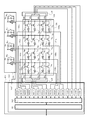
図2は、撮像装置100の構成例を示す図である。なお、図1を用いて説明した構成と同じものは同じ番号を付与してあり、詳細な説明は割愛する。検出部101は、行列状に複数配置された画素201を有する。図2には、8行8列にわたって8×8個の画素201が配置されている。複数の画素201は、それぞれ、放射線又は光を電荷に変換する変換素子Sと、変換素子Sの電荷に基づく電気信号を信号配線Sigに出力するスイッチ素子Tとを有し、2次元行列状に配列されている。光を電荷に変換する変換素子Sとしては、ガラス基板等の絶縁性基板上に配置され、アモルファスシリコンを主材料とするPIN型フォトダイオードやMIS型フォトダイオードなどの光電変換素子を用いることができる。放射線を電荷に変換する変換素子としては、上述の光電変換素子の放射線入射側に放射線を光電変換素子が感知可能な波長帯域の光に変換する波長変換体を備えた間接型の変換素子や、放射線を直接電荷に変換する直接型の変換素子を用いることができる。スイッチ素子Tとしては、制御端子と2つの主端子を有するトランジスタを用いることができ、光電変換素子Sが絶縁性基板上の備えられる画素の場合には、薄膜トランジスタ(TFT)を用いることができる。変換素子Sの一方の電極はスイッチ素子Tの2つの主端子のうちの一方に電気的に接続され、他方の電極は共通の配線を介してセンサバイアス配線VS1〜VS8と電気的に接続される。センサバイアス配線VS1〜VS8にはセンサバイアスVsが供給され、センサバイアス配線VS1〜VS8は変換素子SにセンサバイアスVsを供給する。行方向の複数の画素のスイッチ素子T、例えばT11〜T18は、それらの制御端子が1行目の駆動配線G1に共通に電気的に接続されている。駆動回路102からスイッチ素子Tの導通状態を制御する駆動信号が、駆動配線Gを介して行単位で与えられる。列方向の複数の画素のスイッチ素子T、例えばT11〜T81は、それらの他方の主端子が1列目の信号配線Sig1に電気的に接続されている。スイッチ素子Tが導通状態になっている間に、変換素子Sの電荷に応じた電気信号が、信号配線Sigを介して読出回路103に出力される。
FIG. 2 is a diagram illustrating a configuration example of the
第1の実施形態では、水平方向に延びる駆動配線G1〜G8及び垂直方向に延びるセンサバイアス配線VS1〜VS8は、AECモニタ部508に接続されている。AECモニタ部508は、X線照射中に駆動配線G1〜G8及びセンサバイアス配線VS1〜VS8に流れる電流をモニタ(検出)する。列方向に複数配列された信号配線Sig1〜Sig8は、検出部101の複数の画素201から出力された電気信号を並列に読出回路部103に伝送する。本実施形態では、検出部101は4画素列分を一組とする第1の画素群101a及び第2の画素群101bに分割されている。第1の画素群101aから出力されたアナログ電気信号は、読出回路103内の対応する第1の読出回路103aによって並列に読み出され、第2の画素群101bから出力されたアナログ電気信号は、第2の読出回路103bによって並列に読み出される。
In the first embodiment, the drive wirings G 1 to G 8 extending in the horizontal direction and the sensor bias wirings VS 1 to VS 8 extending in the vertical direction are connected to the
図3は、第1の読出回路103aの構成例を示す図である。以下、第1の読出回路103aの構成を例に説明するが、第2の読出回路103bの構成も第1の読出回路103aの構成と同様である。第1の読出回路103aは、第1の画素群101aから並列に出力された電気信号を増幅する第1の増幅回路部202aと、第1の増幅回路部202aからの電気信号をサンプルしホールドするための第1のサンプルホールド回路部203aとを有する。第2の読出回路103bも同様に、第2の増幅回路部202bと、第2のサンプルホールド回路部203bとを有する。第1及び第2の増幅回路部202a及び202bは、それぞれ、読み出された電気信号を増幅して出力する演算増幅器Aと、積分容量群Cfと、積分容量CfをリセットするリセットスイッチRCとを有し、各信号配線Sigに対応して設けられる。演算増幅器Aの反転入力端子には信号配線Sigの電気信号が入力され、演算増幅器Aの出力端子からは増幅された電気信号が出力される。ここで、演算増幅器Aの正転入力端子には、基準電圧Vref1が入力される。第1及び第2のサンプルホールド回路部203a及び203bは、サンプリングスイッチSHON,SHEN,SHOS,SHESと、サンプリング容量Chon,Chen,Chos,Chesとを有し、各増幅回路部202a,202bに対応して設けられる。また、第1の読出回路103aは、第1のサンプルホールド回路部203aから並列に読み出された電気信号を、それぞれ順次出力して直列信号の画像信号として出力する第1のマルチプレクサ204aを有する。同様に、第2の読出回路103bは、第2のサンプルホールド回路部203bから並列に読み出された電気信号を、それぞれ順次出力して直列信号の画像信号として出力する第2のマルチプレクサ204bを有する。第1のマルチプレクサ204aは、サンプリング容量Chon,Chen,Chos,Chesに対応してスイッチMSON,MSEN,MSOS,MSESを有し、各スイッチを順次選択することにより、並列信号を直列信号に変換する。さらに、第1の読出回路103aは、第1のマルチプレクサ204aの出力信号をインピーダンス変換して出力する出力バッファ回路SFN,SFSと、スイッチSRN,SRSと、第1の可変増幅器205aとを有する。図2において、A/D変換器104aは、第1の可変増幅器205aの出力信号をアナログからデジタルに変換し、信号処理回路105に画像データを出力する。
FIG. 3 is a diagram illustrating a configuration example of the
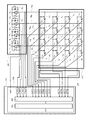
図4は、本発明の第1の実施形態に係る撮像装置100の構成例を示す図である。なお、図2を用いて説明した構成と同じものは同じ番号を付与してあり、詳細な説明は割愛する。AECモニタ部508は、センサバイアス電流モニタ回路部MVS1〜MVS8、駆動配線電流モニタ回路部MVG1〜MVG8、フィルタ部560及び演算部561を有する。センサバイアス電流モニタ回路部MVS1〜MVS8は、センサバイアス配線VS1〜VS8に流れる電流をモニタする。駆動配線電流モニタ回路部MVG1〜MVG8は、駆動配線G1〜G8に流れる電流をモニタする。フィルタ部560は、センサバイアス電流モニタ回路部MVS1〜MVS8及び駆動配線電流モニタ回路部MVG1〜MVG8のモニタ出力結果にフィルタ処理を施す。演算部561は、フィルタ部560の出力結果を逆投影処理し、関心領域の値を演算し、関心領域の値があらかじめ設定した閾値を超えている場合は、X線照射を停止させる停止信号551を制御部108へ出力する。また、関心領域情報及び閾値情報は、モニタ条件信号550により制御部108からAECモニタ部508へ出力される。
FIG. 4 is a diagram illustrating a configuration example of the
バイアス電流モニタ回路部MVS1〜MVS8は、トランスインピーダンスアンプmamp1、フィードバック抵抗MRF1及びMRF2、スイッチMSW、計装アンプmamp2、並びにADコンバータMADCを有する。同様に、駆動配線電流モニタ回路部MVG1〜MVG8は、トランスインピーダンスアンプmamp1、フィードバック抵抗MRF1及びMRF2、スイッチMSW、計装アンプmamp2、並びにADコンバータMADCを有する。トランスインピーダンスアンプmamp1は、センサバイアス配線VS1〜VS8又は駆動配線G1〜G8に流れる電流を電圧に変換する。フィードバック抵抗MRF1及びMRF2は、電流を電圧に変換する際の変換ゲインを設定する。計装アンプmamp2は、トランスインピーダンスアンプmamp1で変換された電圧にさらにゲインを掛ける。ADコンバータMADCは、計装アンプmamp2からの電圧値をアナログからデジタルに変換する。AEC機能を実現するには、ADコンバータMADCの入力範囲内に信号が入らないと正しくモニタすることができない。そのため、ADコンバータMADCがオーバーフローした際に電流−電圧変換ゲインを下げるためのゲイン切換えスイッチMSWが設けられる。これにより、オーバーフロー信号OFによりスイッチMSWを切換えるAGC(Automatic Gain Control)が実現される。 The bias current monitor circuit units MVS 1 to MVS 8 include a transimpedance amplifier mamp1, feedback resistors MRF1 and MRF2, a switch MSW, an instrumentation amplifier mamp2, and an AD converter MADC. Similarly, the drive wiring current monitor circuit units MVG 1 to MVG 8 include a transimpedance amplifier mamp1, feedback resistors MRF1 and MRF2, a switch MSW, an instrumentation amplifier mamp2, and an AD converter MADC. The transimpedance amplifier mamp1 converts the current flowing through the sensor bias lines VS 1 to VS 8 or the drive lines G 1 to G 8 into a voltage. The feedback resistors MRF1 and MRF2 set a conversion gain when converting a current into a voltage. The instrumentation amplifier mamp2 further applies a gain to the voltage converted by the transimpedance amplifier mamp1. The AD converter MADC converts the voltage value from the instrumentation amplifier mamp2 from analog to digital. In order to realize the AEC function, monitoring cannot be performed correctly unless a signal enters the input range of the AD converter MADC. Therefore, a gain changeover switch MSW is provided for reducing the current-voltage conversion gain when the AD converter MADC overflows. Thereby, an AGC (Automatic Gain Control) for switching the switch MSW by the overflow signal OF is realized.
図5は本発明の第1の実施形態に係る撮像装置のフローチャートであり、図6(a)〜(d),図7(a)〜(c)、図8は、モニタ出力結果の処理方法を示したものである。図5のフローチャートを参照しながら、第1の実施形態の動作について説明する。ステップS301では、撮影前に技師によりAECのモニタ位置(関心領域)を指定する。X線制御装置502は、指定したモニタ位置でX線量が最適な量になるようにX線発生装置501の制御を行う。モニタ位置の指定は、技師により指定するもしくは撮影部位を指定することにより自動的にモニタ位置を決定することができる。指定されたモニタ位置情報は、モニタ条件信号550で制御部108からAECモニタ部508へ出力される。
FIG. 5 is a flowchart of the imaging apparatus according to the first embodiment of the present invention. FIGS. 6A to 6D, FIGS. 7A to 7C, and FIG. Is shown. The operation of the first embodiment will be described with reference to the flowchart of FIG. In step S301, an AEC monitor position (region of interest) is designated by an engineer before imaging. The
ステップS302では、撮影が開始される。ステップS303では、検出部101にセンサバイアス配線VS1〜VS8に電圧が供給され、撮像装置100はアイドリング(K)を行う。アイドリング(K)は、駆動配線G1〜G8を順次動作させ、スイッチ素子Tを行単位にオンし、変換素子Sに流れる暗電流のリセットを行う。次に、ステップS304では、X線照射スイッチ503が押される。次に、ステップS305では、最終駆動配線G8までリセット動作を行い、蓄積動作(W)に移行する。次に、ステップS306では、AECモニタ部508は、センサバイアス配線VS1〜VS8及び駆動配線G1〜G8に流れる電流のモニタを開始する。変換素子SにX線(光)が照射されると、変換素子Sに電子及び正孔が生成されるが、蓄積動作(W)期間中は、スイッチ素子Tがオフしているため、発生した電子及び正孔のほとんどが外部回路へは流れず、変換素子Sに蓄積される。一部、スイッチ素子Tの寄生容量に依存した電流がセンサバイアス配線VS1〜VS8及び駆動配線G1〜G8へ流れ、この電流を測定することにより蓄積動作(W)中に照射されたX線量をモニタする。
In step S302, shooting is started. In step S303, a voltage is supplied to the sensor bias line VS 1 ~VS 8 to the
センサバイアス配線VS1には、センサバイアス配線VS1に接続された変換素子S11〜S81に照射されたX線量に比例する量の電流が流れ、駆動配線G1には、変換素子S11〜S18に照射されたX線量に比例する量の電流が流れる。流れた電流はトランスインピーダンスアンプmamp1、計装アンプmamp2、ADコンバータMADCを介して、デジタル値に変換される。図6(a)は、センサバイアス配線VS1〜VS8に流れる電流、図6(b)は、駆動配線G1〜G8に流れる電流を表わしている。ステップS307では、バイアス電流モニタ回路部MVS1〜MVS8及び駆動配線電流モニタ回路部MVG1〜MVG8は、それぞれ、センサバイアス配線VS1〜VS8及び駆動配線G1〜G8に流れる電流のデジタル値を出力する。 The sensor bias line VS 1, the amount of current flows in proportion to the amount of X-rays irradiated to the conversion element S 11 to S 81, which is connected to the sensor bias line VS 1, the drive wire G 1, transducer S 11 the amount of current proportional to the X-rays irradiated on the to S 18 flows. The flowing current is converted into a digital value via the transimpedance amplifier mamp1, the instrumentation amplifier mamp2, and the AD converter MADC. 6A shows the current flowing through the sensor bias lines VS 1 to VS 8 , and FIG. 6B shows the current flowing through the drive lines G 1 to G 8 . In step S307, the bias current monitor circuit units MVS 1 to MVS 8 and the drive wiring current monitor circuit units MVG 1 to MVG 8 are respectively connected to the sensor bias wirings VS 1 to VS 8 and the drive wirings G 1 to G 8 . Outputs a digital value.
次に、ステップS308では、フィルタ部560は、バイアス電流モニタ回路部MVS1〜MVS8及び駆動配線電流モニタ回路部MVG1〜MVG8から出力されたデジタル値をフィルタ処理する。バイアス電流モニタ回路部MVS1〜MVS8及び駆動配線電流モニタ回路部MVG1〜MVG8から出力されたデジタル値は、低周波のノイズ成分を多くもっているため、フィルタ部560のハイパスフィルタを介して低周波成分を取り除く。フィルタ部560から出力された値を図6(c)及び(d)に示す。図6(c)は、センサバイアス配線VS1〜VS8の電流、図6(d)は、駆動配線G1〜G8の電流を表わしている。
Next, in step S308, the
次に、ステップS309では、演算部561は、フィルタ部560の出力値に対して、2次元データにするため、垂直方向に延びるセンサバイアス配線VS1〜VS8についての逆投影処理を行う。図7(a)は、センサバイアス配線VS1〜VS8ついての逆投影処理を示したものであり、2次元メモリ上にフィルタ部560から出力された1次元の出力結果を逆投影する。逆投影処理を行う際、バイアス電流モニタ回路部MVS1〜MVS8及び駆動配線電流モニタ回路部MVG1〜MVG8から出力されたデジタル値は、1列もしくは1行を積算した値になっているため、それぞれ、行数、列数で割った値を逆投影処理する。
Next, in step S309, the
次に、ステップS310では、演算部561は、図7(b)に示すように、水平方向に延びる駆動配線G1〜G8についての逆投影処理を行う。次に、演算部561は、ステップS311では、垂直方向に延びるセンサバイアス配線VS1〜VS8についての逆投影処理の結果(図7(a))に、垂直方向に延びる駆動配線G1〜G8についての逆投影結果を加算する。フィルタ処理や逆投影処理については、CT装置で行われる再構成処理と同様の方法で行う。垂直方向に延びるセンサバイアス配線VS1〜VS8についての逆投影処理及び水平方向に延びる駆動配線G1〜G8についての逆投影処理を行うことにより、被写体を透過したX線の2次元分布を求めることができる。すなわち、バイアス電流モニタ回路部MVS1〜MVS8及び駆動配線電流モニタ回路部MVG1〜MVG8は、複数の画素201に接続される2つの異なる方向に延びるセンサバイアス配線VS1〜VS8及び駆動配線G1〜G8に流れる電流をモニタする。演算部561は、2つの異なる方向に延びるセンサバイアス配線VS1〜VS8及び駆動配線G1〜G8に流れる電流を逆投影処理することにより、2次元分布を演算する。次に、演算部561は、AEC機能を実現するには、モニタ位置(関心領域)のX線量の積算値を算出する必要があるため、図7(c)に示すように、図7(b)の逆投影処理結果を加算メモリに積算する。
Next, in step S310, the
次に、ステップS312では、演算部561は、図8に示すように、図7(c)の加算処理後の加算メモリの値に被写体補正係数を乗算することにより、被写体補正処理を行う。撮影する部位によっては、検出器101に対し一部に大きなX線が照射され、該当する列もしくは行の出力が大きくなってしまい、同じ列の中のX線量の小さい部分の値が正確に読み取れなくなる。そのため、撮影部位により、あらかじめ被写体補正係数を算出し、乗算することより、精度良く関心領域のX線量をモニタすることができる。図8は、胸部の撮影の例を示している。胸部撮影では、胴体の脇の部分でX線吸収が無いため出力が大きくなる(図8の1列及び8列の5行〜8行の領域)。しかし、駆動配線G1〜G8には、1行の合計の電流が流れるため、1行が平均化されたように見える。そのため、逆投影処理を行うと、出力が大きい箇所は小さく、出力が小さい箇所は大きな値となる。撮影部位により、領域での出力の大小関係は決まるため、あらかじめ被写体補正係数を算出して補正することが可能となる。
Next, in step S312, the
次に、ステップS313では、演算部561は、あらかじめ設定されたモニタ位置で、被写体補正後の値が閾値を超えているか否かを判定し、超えていない場合は、ステップS307に戻り、モニタを続ける。閾値を超えている場合は、ステップS314において、演算部561は、X線照射を停止させるための停止信号551を制御部108へ出力し、制御部108はX線制御装置502を介してX線発生装置501のX線照射(放射線照射)を中止させる。判定方法は、あらかじめユーザーがモニタ位置を指定する、又は撮影部位によりモニタ位置を決定するなどがある。また、モニタ位置の大きさは、1領域(例えば、行3、列3)、複数領域(例えば、行3〜5、列3〜6)の平均値、最大値、最小値のいずれかと閾値を比較するなどがある。また、閾値もある1つの閾値を持つ、もしくは、行列状に領域で異なる閾値を持ち、どこか1つでも閾値を超える、全て閾値を超える、半分以上が閾値を超えるとX線を停止させるなどの方法がある。X線照射が中止された後は、ステップS315において、撮像装置100は、診断で使用される被写体画像の読出し動作を開始する。
Next, in step S313, the
このように、センサバイアス配線VS1〜VS8及び駆動配線G1〜G8に流れる電流をモニタし、逆投影処理をすることにより、被写体を透過した関心領域のX線量を求めることができる。求められたX線量から、関心領域のX線量が最適になるようX線発生装置501を制御することにより、AEC機能が実現できる。
As described above, by monitoring the current flowing through the sensor bias wirings VS 1 to VS 8 and the driving wirings G 1 to G 8 and performing the back projection process, the X-ray dose of the region of interest that has passed through the subject can be obtained. The AEC function can be realized by controlling the
(第2の実施形態)
図9は、本発明の第2の実施形態に係る撮像装置100の構成例を示す図である。なお、第1の実施形態において説明した構成と同じものは同じ番号を付与してあり、詳細な説明は割愛する。第1の実施形態においては、センサバイアス配線VS1〜VS8が1列共通に配線され、駆動配線G1〜G8が1行共通に配線していた。検出器101に対して、1部に大きなX線が照射されると、該当する列もしくは行の出力が大きくなってしまい、同じ列の中のX線量の小さい部分の値が正確に読み取れなくなる。そのため、第2の実施形態では、センサバイアス配線VS1〜VS8をセンサバイアス配線VSU1〜VSU8及びVSD1〜VSD8の上下に2分割し、駆動配線G1〜G8を駆動配線GR1〜GR8及びGL1〜GL8の左右に2分割する。これにより、本実施形態は、計4ブロックに検出器101を分割している。そのため、検出器101の一部に大きなX線が照射されても、他のブロックではX線を正確にモニタすることが可能となる。駆動回路102は、駆動配線GR1〜GR8及びGL1〜GL8に駆動信号を供給する。センサバイアス電流モニタ回路部MVSU1〜MVSU8は、センサバイアス配線VSU1〜VSU8に流れる電流をモニタし、フィルタ部560に出力する。センサバイアス電流モニタ回路部MVSD1〜MVSD8は、センサバイアス配線VSD1〜VSD8に流れる電流をモニタし、フィルタ部560に出力する。駆動配線電流モニタ回路部MVGL1〜MVGL8は、駆動配線GL1〜GL8に流れる電流をモニタし、フィルタ部560に出力する。駆動配線電流モニタ回路部MVGR1〜MVGR8は、駆動配線GR1〜GR8に流れる電流をモニタし、フィルタ部560に出力する。
(Second Embodiment)
FIG. 9 is a diagram illustrating a configuration example of the
上記のように、電流モニタ回路部は、2つ以上の異なる方向に延びる配線のうちの少なくとも1つの配線について、複数の画素201が分割された領域毎に電流をモニタするようにしてもよい。
As described above, the current monitor circuit unit may monitor the current for each region where the plurality of
(第3の実施形態)
図10は、本発明の第3の実施形態に係る撮像装置100の構成例を示す図である。なお、第1の実施形態において説明した構成と同じものは同じ番号を付与してあり、詳細な説明は割愛する。第1の実施形態においては、センサバイアス配線VS1〜VS8と駆動配線G1〜G8が直交した配線になっているため、逆投影処理を2方向から行っていた。第3の実施形態では、センサバイアス配線VS1〜VS7を斜め方向に配線する。センサバイアス電流モニタ回路部MVS1〜MVS7は、斜め方向に延びるセンサバイアス配線VS1〜VSD7に流れる電流をモニタし、フィルタ部560に出力する。駆動配線電流モニタ回路部MVG1〜MVG4は、水平方向に延びる駆動配線G1〜G4に流れる電流をモニタし、フィルタ部560に出力する。
(Third embodiment)
FIG. 10 is a diagram illustrating a configuration example of an
さらに、スイッチR1〜R4は、それぞれ、演算増幅器A1〜A4の正転入力端子及び出力端子間に接続される。信号配線電流モニタ回路部MVi1〜MVi4は、上記のセンサバイアス電流モニタ回路部MVS1〜MVS7と同じ構成を有し、垂直方向に延びる信号配線Sig1〜Sig4に流れる電流をモニタし、フィルタ部560に出力する。センサバイアス電流モニタ回路部MVS1〜MVS7、駆動配線電流モニタ回路部MVG1〜MVG4及び信号配線電流モニタ回路部MVi1〜MVi4が電流をモニタすることにより、演算部561は3つの異なる方向の配線の逆投影処理を行う。逆投影処理は、逆投影処理の方向を多くするほど2次元分布が正確に求めることが可能となる。また、図11に示すように、逆投影処理も斜め方向に行うが、積算している画素数が配線により異なるため、積算している画素数で割る必要がある。
Furthermore, the switches R 1 to R 4 are connected between the normal input terminal and the output terminal of the operational amplifiers A 1 to A 4 , respectively. Signal wire current monitoring circuit unit MVi1~MVi4 has the same structure as the sensor bias current monitoring circuit unit MVS 1 ~MVS 7, monitors the current flowing through the signal lines Sig 1 to Sig 4 extending in the vertical direction, the filter To the
なお、電流モニタ回路部は、信号配線Sig1〜Sig4、センサバイアス配線VS1〜VS7及び駆動配線G1〜G8のうちの2つ以上の異なる方向に延びる配線に流れる電流をモニタするようにしてもよい。その場合、演算部561は、電流モニタ回路部によりモニタされた2つ以上の異なる方向に延びる配線に流れる電流を逆投影処理することにより、2次元分布を演算する。
The current monitor circuit unit monitors currents flowing in two or more of the signal wirings Sig 1 to Sig 4 , the sensor bias wirings VS 1 to VS 7, and the driving wirings G 1 to G 8 that extend in different directions. You may do it. In that case, the
(第4の実施形態)
図12は、本発明の第4の実施形態に係る画素201(図2)の構成例を示す図である。なお、第3の実施形態において説明した構成と同じものは同じ番号を付与してあり、詳細な説明は割愛する。図12に示すように、ダミー配線Vdは、容量Cdを介して、変換素子Sとスイッチ素子Tとの相互接続点に接続される。これにより、照射されたX線による電流をダミー配線Vdを介して外部回路に取り出すことができる。
(Fourth embodiment)
FIG. 12 is a diagram illustrating a configuration example of the pixel 201 (FIG. 2) according to the fourth embodiment of the present invention. The same components as those described in the third embodiment are denoted by the same reference numerals, and detailed description thereof is omitted. As shown in FIG. 12, the dummy wiring Vd is connected to an interconnection point between the conversion element S and the switch element T via a capacitor Cd. Thereby, the current by the irradiated X-rays can be taken out to the external circuit via the dummy wiring Vd.
図13は、本発明の第4の実施形態に係る撮像装置の構成例を示す図であり、ダミー配線Vdの検出器101内の配線方法を示している。ダミー配線Vd1〜Vd7は、センサバイアス配線VS1〜VS7に対して直交するように配置され、行列状の画素201の容量Cdに対して斜め方向に接続される。ダミー配線電流モニタ回路部MVD1〜MVD7は、上記のセンサバイアス電流モニタ回路部MVS1〜MVS7及び駆動配線電流モニタ回路部MVG1〜MVG4と同じ構成を有し、ダミー配線VS1〜VS7に流れる電流をモニタし、フィルタ部560に出力する。センサバイアス電流モニタ回路部MVS1〜MVS7、駆動配線電流モニタ回路部MVG1〜MVG4、信号配線電流モニタ回路部MVi1〜MVi4及びダミー配線電流モニタ回路部MVD1〜MVD7が電流をモニタする。これにより、演算部561は4つの異なる方向の配線の逆投影処理を行うことができ、2次元分布をより正確に求めることが可能となる。さらに、第2の実施形態のように、ブロックに分割して、4方向から配線を引き出すことにより、2次元分布をより正確に求めることが可能となる。
FIG. 13 is a diagram illustrating a configuration example of an imaging apparatus according to the fourth embodiment of the present invention, and illustrates a wiring method in the
なお、電流モニタ回路部は、信号配線Sig1〜Sig4、センサバイアス配線VS1〜VS7、駆動配線G1〜G8及びダミー配線Vd1〜Vd7のうちの2つ以上の異なる方向に延びる配線に流れる電流をモニタするようにしてもよい。その場合、演算部561は、電流モニタ回路部によりモニタされた2つ以上の異なる方向に延びる配線に流れる電流を逆投影処理することにより、2次元分布を演算する。
Note that the current monitor circuit section is provided in two or more different directions of the signal wirings Sig 1 to Sig 4 , the sensor bias wirings VS 1 to VS 7 , the driving wirings G 1 to G 8, and the dummy wirings Vd 1 to Vd 7. You may make it monitor the electric current which flows into the extended wiring. In that case, the
(第5の実施形態)
図14は、本発明の第5の実施形態に係る撮像装置の構成例を示す図である。なお、第1の実施形態において説明した構成と同じものは同じ番号を付与してあり、詳細な説明は割愛する。第1の実施形態では、検出器101の全面のセンサバイアス配線VS及び駆動配線Gをモニタしていたが、第5の実施形態では、モニタ位置のセンサバイアス配線VSに流れる電流と駆動配線Gに流れる電流だけを計測している。制御部108からAECモニタ部508に出力されるモニタ条件信号550により、列選択スイッチMSW3及び行選択スイッチMSW4をモニタ位置に合わせ、モニタ位置のみを計測する。列選択スイッチMSW3は、センサバイアス電流モニタ回路部MVSを、モニタ位置の列のセンサバイアス配線VSに選択的に接続する。行選択スイッチMSW4は、駆動配線電流モニタ回路部MVGを、モニタ位置の行の駆動配線Gに選択的に接続する。このようにすることにより、回路の規模を小さくでき、消費電力が小さくなり、装置の大型化を防止することができる。
(Fifth embodiment)
FIG. 14 is a diagram illustrating a configuration example of an imaging apparatus according to the fifth embodiment of the present invention. In addition, the same thing as the structure demonstrated in 1st Embodiment is provided with the same number, and detailed description is omitted. In the first embodiment, the sensor bias wiring VS and the drive wiring G on the entire surface of the
なお、上記実施形態は、何れも本発明を実施するにあたっての具体化の例を示したものに過ぎず、これらによって本発明の技術的範囲が限定的に解釈されてはならないものである。すなわち、本発明はその技術思想、又はその主要な特徴から逸脱することなく、様々な形で実施することができる。 The above-described embodiments are merely examples of implementation in carrying out the present invention, and the technical scope of the present invention should not be construed in a limited manner. That is, the present invention can be implemented in various forms without departing from the technical idea or the main features thereof.
100 撮像装置、201 画素、MVS,MVG 電流モニタ回路部、561 演算部、S 変換素子、T スイッチ素子
DESCRIPTION OF
Claims (7)
前記複数の画素に接続された、互いに異なる方向に延びる2つ以上の配線に流れる電流をモニタする電流モニタ回路と、
前記電流モニタ回路によりモニタされた前記2つ以上の配線に流れる電流を逆投影処理することにより、2次元分布を演算する演算部と、
を有することを特徴とする撮像装置。 A plurality of pixels arranged in a matrix for converting radiation into an electrical signal ;
Connected to said plurality of pixels, and a current monitoring circuit for monitoring the current flowing through the two or more wirings extending in different directions,
A computing unit that computes a two-dimensional distribution by performing back projection processing on the current flowing through the two or more wires monitored by the current monitoring circuit ;
An imaging device comprising:
前記2つ以上の配線は、前記信号配線と、前記変換素子にバイアスを供給するセンサバイアス配線と、前記スイッチ素子を制御するための駆動配線と、を含み、
前記電流モニタ回路は、前記信号配線、前記センサバイアス配線及び前記駆動配線のうちの2つ以上の異なる方向に延びる配線に流れる電流をモニタすることを特徴とする請求項1記載の撮像装置。 The pixel includes a conversion element for converting the radiation or light corresponding to the radiation into an electric charge, and a switch element that outputs the electric signal based on the electric charge to a signal wiring ,
The two or more wires includes said signal lines, and the sensor bias line for supplying a bias to the conversion element, and a driving wiring for controlling the switch element,
The imaging apparatus according to claim 1, wherein the current monitor circuit monitors a current flowing in a wiring extending in two or more different directions among the signal wiring, the sensor bias wiring, and the driving wiring.
前記電流モニタ回路は、前記信号配線、前記センサバイアス配線、前記駆動配線及び前記ダミー配線のうちの2つ以上の異なる方向に延びる配線に流れる電流をモニタすることを特徴とする請求項2記載の撮像装置。 The two or more wirings further include a dummy wiring connected to the conversion element via a capacitor,
The current monitor circuit, the signal line, the sensor bias line, according to claim 2, wherein monitoring the current flowing through the two or more different directions to extend the wiring of the drive wiring and the dummy wiring Imaging device.
前記撮像装置に放射線の照射を行う放射線発生装置と、
前記放射線発生装置を制御するための制御装置と、
を有する撮像システムであって、
前記演算部は、前記演算された2次元分布に基づいて、前記制御装置を介して前記放射線発生装置の放射線照射を中止させるための信号を出力することを特徴とする撮像システム。 The imaging device according to any one of claims 1 to 6,
A radiation generator for irradiating the imaging device with radiation;
A control device for controlling the radiation generating device;
An imaging system comprising:
The said calculating part outputs the signal for stopping the radiation irradiation of the said radiation generation apparatus via the said control apparatus based on the calculated two-dimensional distribution, The imaging system characterized by the above-mentioned.
Priority Applications (2)
| Application Number | Priority Date | Filing Date | Title |
|---|---|---|---|
| JP2012288451A JP6041669B2 (en) | 2012-12-28 | 2012-12-28 | Imaging apparatus and imaging system |
| US14/138,918 US9462989B2 (en) | 2012-12-28 | 2013-12-23 | Imaging apparatus and imaging system |
Applications Claiming Priority (1)
| Application Number | Priority Date | Filing Date | Title |
|---|---|---|---|
| JP2012288451A JP6041669B2 (en) | 2012-12-28 | 2012-12-28 | Imaging apparatus and imaging system |
Publications (3)
| Publication Number | Publication Date |
|---|---|
| JP2014131214A JP2014131214A (en) | 2014-07-10 |
| JP2014131214A5 JP2014131214A5 (en) | 2016-02-12 |
| JP6041669B2 true JP6041669B2 (en) | 2016-12-14 |
Family
ID=51017208
Family Applications (1)
| Application Number | Title | Priority Date | Filing Date |
|---|---|---|---|
| JP2012288451A Active JP6041669B2 (en) | 2012-12-28 | 2012-12-28 | Imaging apparatus and imaging system |
Country Status (2)
| Country | Link |
|---|---|
| US (1) | US9462989B2 (en) |
| JP (1) | JP6041669B2 (en) |
Families Citing this family (43)
| Publication number | Priority date | Publication date | Assignee | Title |
|---|---|---|---|---|
| JP5814621B2 (en) | 2011-05-24 | 2015-11-17 | キヤノン株式会社 | IMAGING DEVICE, ITS CONTROL METHOD, AND IMAGING SYSTEM |
| JP5583191B2 (en) * | 2011-11-25 | 2014-09-03 | 富士フイルム株式会社 | Radiation image detection apparatus and operation method thereof |
| JP5986524B2 (en) | 2013-02-28 | 2016-09-06 | キヤノン株式会社 | Radiation imaging apparatus and radiation imaging system |
| JP6016673B2 (en) | 2013-02-28 | 2016-10-26 | キヤノン株式会社 | Radiation imaging apparatus and radiation imaging system |
| JP5934128B2 (en) | 2013-02-28 | 2016-06-15 | キヤノン株式会社 | Radiation imaging apparatus and radiation imaging system |
| KR20160038387A (en) * | 2014-09-30 | 2016-04-07 | 주식회사 레이언스 | X-ray detector and driving method thereof |
| WO2016197297A1 (en) * | 2015-06-08 | 2016-12-15 | 北京旷视科技有限公司 | Living body detection method, living body detection system and computer program product |
| KR101689880B1 (en) * | 2015-06-12 | 2016-12-27 | 주식회사 뷰웍스 | X-ray imaging apparatus |
| JP6573377B2 (en) | 2015-07-08 | 2019-09-11 | キヤノン株式会社 | Radiation imaging apparatus, control method thereof, and program |
| JP6573378B2 (en) | 2015-07-10 | 2019-09-11 | キヤノン株式会社 | Radiation imaging apparatus, control method thereof, and program |
| JP6643871B2 (en) | 2015-11-13 | 2020-02-12 | キヤノン株式会社 | Radiation imaging apparatus and photon counting method |
| JP6587517B2 (en) | 2015-11-13 | 2019-10-09 | キヤノン株式会社 | Radiation imaging system |
| JP6663210B2 (en) | 2015-12-01 | 2020-03-11 | キヤノン株式会社 | Radiation imaging apparatus and control method thereof |
| JP6643909B2 (en) | 2016-01-27 | 2020-02-12 | キヤノン株式会社 | Radiation imaging apparatus, control method thereof, and program |
| JP6706963B2 (en) | 2016-04-18 | 2020-06-10 | キヤノン株式会社 | Radiation imaging apparatus, radiation imaging system, and control method for radiation imaging apparatus |
| JP6695260B2 (en) * | 2016-11-02 | 2020-05-20 | 富士フイルム株式会社 | Radiation image capturing apparatus, radiation image capturing method, and radiation image capturing program |
| JP6871717B2 (en) | 2016-11-10 | 2021-05-12 | キヤノン株式会社 | Radiation imaging device, radiation imaging system and radiation imaging method |
| JP6461212B2 (en) | 2017-02-01 | 2019-01-30 | キヤノン株式会社 | Radiation imaging apparatus and radiation imaging system |
| JP6974948B2 (en) | 2017-02-10 | 2021-12-01 | キヤノン株式会社 | Radiation imaging device and radiation imaging method |
| JP6929104B2 (en) | 2017-04-05 | 2021-09-01 | キヤノン株式会社 | Radiation imaging device, radiation imaging system, control method and program of radiation imaging device |
| JP6853729B2 (en) | 2017-05-08 | 2021-03-31 | キヤノン株式会社 | Radiation imaging device, radiation imaging system, control method and program of radiation imaging device |
| JP6788547B2 (en) | 2017-05-09 | 2020-11-25 | キヤノン株式会社 | Radiation imaging device, its control method, control device, and radiation imaging system |
| WO2019012846A1 (en) | 2017-07-10 | 2019-01-17 | キヤノン株式会社 | Radiation imaging device and radiation imaging system |
| JP6934769B2 (en) | 2017-07-28 | 2021-09-15 | キヤノン株式会社 | Radiation imaging device and radiation imaging method |
| JP6912965B2 (en) | 2017-08-04 | 2021-08-04 | キヤノン株式会社 | How to operate a radiation imaging device, a radiation imaging system, and a radiation imaging device |
| JP7038506B2 (en) | 2017-08-25 | 2022-03-18 | キヤノン株式会社 | How to operate a radiation image pickup device, a radiation image pickup system, and a radiation image pickup device |
| JP6882135B2 (en) | 2017-10-06 | 2021-06-02 | キヤノン株式会社 | Image processing equipment, image processing methods and programs |
| JP7045834B2 (en) | 2017-11-10 | 2022-04-01 | キヤノン株式会社 | Radiation imaging system |
| JP7067912B2 (en) | 2017-12-13 | 2022-05-16 | キヤノン株式会社 | Radiation imaging device and radiation imaging system |
| JP7245001B2 (en) | 2018-05-29 | 2023-03-23 | キヤノン株式会社 | Radiation imaging device and imaging system |
| JP7093233B2 (en) | 2018-06-07 | 2022-06-29 | キヤノン株式会社 | Radiography equipment, radiography methods and programs |
| WO2020003744A1 (en) | 2018-06-27 | 2020-01-02 | キヤノン株式会社 | Radiographic imaging apparatus, radiographic imaging method, and program |
| JP6818724B2 (en) | 2018-10-01 | 2021-01-20 | キヤノン株式会社 | Radiation imaging device, its control method and radiation imaging system |
| JP7170497B2 (en) | 2018-10-22 | 2022-11-14 | キヤノン株式会社 | Radiation imaging device and radiation imaging system |
| JP7319809B2 (en) * | 2019-03-29 | 2023-08-02 | キヤノン株式会社 | Radiation imaging apparatus, its control method, and radiation imaging system |
| JP7319825B2 (en) | 2019-05-17 | 2023-08-02 | キヤノン株式会社 | Radiation imaging device and radiation imaging system |
| JP7361516B2 (en) | 2019-07-12 | 2023-10-16 | キヤノン株式会社 | Radiography device, radiography system, radiography device control method, and program |
| JP7378245B2 (en) | 2019-08-29 | 2023-11-13 | キヤノン株式会社 | Radiation detection device, its control method, and radiation imaging system |
| JP7344769B2 (en) * | 2019-11-22 | 2023-09-14 | キヤノン株式会社 | Radiation detection device and output method |
| JP2021129707A (en) * | 2020-02-19 | 2021-09-09 | コニカミノルタ株式会社 | Imaging control device and radiographic system |
| JP2022022844A (en) | 2020-07-08 | 2022-02-07 | キヤノン株式会社 | Radiation imaging device |
| JP7449260B2 (en) | 2021-04-15 | 2024-03-13 | キヤノン株式会社 | Radiation imaging device and radiation imaging system |
| JP2022164433A (en) | 2021-04-16 | 2022-10-27 | キヤノン株式会社 | Radiation imaging apparatus and radiation imaging system |
Family Cites Families (9)
| Publication number | Priority date | Publication date | Assignee | Title |
|---|---|---|---|---|
| JPH11188021A (en) | 1997-12-26 | 1999-07-13 | Shimadzu Corp | X ray face sensor and radiographic device |
| EP1341375B1 (en) * | 2002-03-01 | 2013-06-05 | Canon Kabushiki Kaisha | Radiation image sensing apparatus and its driving method |
| JP4217443B2 (en) | 2002-08-09 | 2009-02-04 | キヤノン株式会社 | Radiation image capturing apparatus, manufacturing method thereof, and imaging circuit board |
| CN1517069B (en) * | 2003-01-27 | 2012-03-28 | 佳能株式会社 | Radioactive rays camera apparatus and radioactive rays camera system |
| JP4307322B2 (en) | 2004-05-18 | 2009-08-05 | キヤノン株式会社 | Radiation imaging apparatus and radiation imaging system |
| JP2006153616A (en) * | 2004-11-29 | 2006-06-15 | Shimadzu Corp | Radiation-imaging apparatus |
| JP4750512B2 (en) | 2005-09-01 | 2011-08-17 | キヤノン株式会社 | Radiation imaging apparatus, control method therefor, and radiation imaging system |
| JP4847202B2 (en) | 2006-04-27 | 2011-12-28 | キヤノン株式会社 | Imaging apparatus and radiation imaging system |
| JP2011185622A (en) * | 2010-03-05 | 2011-09-22 | Konica Minolta Medical & Graphic Inc | Radiographic imaging apparatus |
-
2012
- 2012-12-28 JP JP2012288451A patent/JP6041669B2/en active Active
-
2013
- 2013-12-23 US US14/138,918 patent/US9462989B2/en active Active
Also Published As
| Publication number | Publication date |
|---|---|
| US20140185764A1 (en) | 2014-07-03 |
| US9462989B2 (en) | 2016-10-11 |
| JP2014131214A (en) | 2014-07-10 |
Similar Documents
| Publication | Publication Date | Title |
|---|---|---|
| JP6041669B2 (en) | Imaging apparatus and imaging system | |
| US10009990B2 (en) | Imaging apparatus, control method therefor, and imaging system | |
| JP5592962B2 (en) | Radiation imaging apparatus, control method therefor, and radiation imaging system | |
| JP6491434B2 (en) | Radiation imaging apparatus and radiation detection system | |
| JP5890286B2 (en) | Radiation image detection device | |
| JP6595803B2 (en) | Radiation imaging apparatus, radiation imaging system and control method thereof | |
| JP6008430B2 (en) | Radiation image detection apparatus and control method thereof | |
| WO2013015266A1 (en) | Radiograph detection device and method for controlling same | |
| JP2008212644A (en) | Radiation imaging apparatus and method of driving the same, and radiation imaging system | |
| JPWO2007037121A1 (en) | Radiation image capturing apparatus and imaging method of radiation image capturing apparatus | |
| JP2014048204A (en) | Radiation imaging apparatus, and radiation imaging system | |
| JP2012119956A (en) | Radiation image detector | |
| JP2012045044A (en) | Radiation image detection device | |
| US8785863B2 (en) | Radiation detection device, control method for radiation detection device, and computer-readable medium | |
| JP2010028387A (en) | Solid-state imaging device | |
| WO2006112320A1 (en) | X-ray plane detector and x-ray image diagnosing device | |
| JP2020065750A (en) | Radiation imaging apparatus and radiation imaging system | |
| JP2010141715A (en) | Image capturing apparatus and system | |
| JP2014068857A (en) | Radiation image photographing control device, radiation moving image photographing system, defect determination method for radiation image photographing apparatus, and radiation image photographing control program | |
| JP6467148B2 (en) | Radiation imaging apparatus and radiation imaging system | |
| JP6701392B2 (en) | Radiation imaging apparatus and radiation imaging system | |
| JP2014068882A (en) | Radiation image photographing control device, radiation moving image photographing system, defect determination method for radiation image photographing apparatus and radiation image photographing control program | |
| JP2011156241A (en) | Radiographic imaging device, and radiographic imaging system | |
| JP5996067B2 (en) | IMAGING DEVICE, ITS CONTROL METHOD, AND IMAGING SYSTEM | |
| JP2024066979A (en) | Radiation imaging apparatus, radiation imaging system, and method for controlling radiation imaging apparatus |
Legal Events
| Date | Code | Title | Description |
|---|---|---|---|
| A521 | Request for written amendment filed |
Free format text: JAPANESE INTERMEDIATE CODE: A523 Effective date: 20151222 |
|
| A621 | Written request for application examination |
Free format text: JAPANESE INTERMEDIATE CODE: A621 Effective date: 20151222 |
|
| A977 | Report on retrieval |
Free format text: JAPANESE INTERMEDIATE CODE: A971007 Effective date: 20160926 |
|
| TRDD | Decision of grant or rejection written | ||
| A01 | Written decision to grant a patent or to grant a registration (utility model) |
Free format text: JAPANESE INTERMEDIATE CODE: A01 Effective date: 20161011 |
|
| A61 | First payment of annual fees (during grant procedure) |
Free format text: JAPANESE INTERMEDIATE CODE: A61 Effective date: 20161108 |
|
| R151 | Written notification of patent or utility model registration |
Ref document number: 6041669 Country of ref document: JP Free format text: JAPANESE INTERMEDIATE CODE: R151 |