JP6037123B2 - Liquid ejecting head, liquid ejecting apparatus, piezoelectric element and sensor - Google Patents
Liquid ejecting head, liquid ejecting apparatus, piezoelectric element and sensor Download PDFInfo
- Publication number
- JP6037123B2 JP6037123B2 JP2013016118A JP2013016118A JP6037123B2 JP 6037123 B2 JP6037123 B2 JP 6037123B2 JP 2013016118 A JP2013016118 A JP 2013016118A JP 2013016118 A JP2013016118 A JP 2013016118A JP 6037123 B2 JP6037123 B2 JP 6037123B2
- Authority
- JP
- Japan
- Prior art keywords
- piezoelectric
- control layer
- orientation control
- layer
- electrode
- Prior art date
- Legal status (The legal status is an assumption and is not a legal conclusion. Google has not performed a legal analysis and makes no representation as to the accuracy of the status listed.)
- Expired - Fee Related
Links
- 239000007788 liquid Substances 0.000 title claims description 26
- 239000000463 material Substances 0.000 claims description 28
- 229910052719 titanium Inorganic materials 0.000 claims description 28
- 229910052742 iron Inorganic materials 0.000 claims description 18
- 239000010410 layer Substances 0.000 description 218
- 239000010936 titanium Substances 0.000 description 61
- 239000010408 film Substances 0.000 description 58
- 239000000758 substrate Substances 0.000 description 58
- XEEYBQQBJWHFJM-UHFFFAOYSA-N iron Substances [Fe] XEEYBQQBJWHFJM-UHFFFAOYSA-N 0.000 description 52
- 239000002243 precursor Substances 0.000 description 51
- 239000000243 solution Substances 0.000 description 48
- 238000000034 method Methods 0.000 description 46
- 239000012212 insulator Substances 0.000 description 16
- VYPSYNLAJGMNEJ-UHFFFAOYSA-N Silicium dioxide Chemical compound O=[Si]=O VYPSYNLAJGMNEJ-UHFFFAOYSA-N 0.000 description 15
- 230000001681 protective effect Effects 0.000 description 15
- 238000005238 degreasing Methods 0.000 description 14
- RTAQQCXQSZGOHL-UHFFFAOYSA-N Titanium Chemical compound [Ti] RTAQQCXQSZGOHL-UHFFFAOYSA-N 0.000 description 13
- 238000002441 X-ray diffraction Methods 0.000 description 13
- 238000001035 drying Methods 0.000 description 13
- 238000000576 coating method Methods 0.000 description 11
- 238000004891 communication Methods 0.000 description 11
- 239000013078 crystal Substances 0.000 description 11
- 238000010304 firing Methods 0.000 description 11
- 229910052751 metal Inorganic materials 0.000 description 11
- 239000002184 metal Substances 0.000 description 11
- 239000000203 mixture Substances 0.000 description 10
- 239000002131 composite material Substances 0.000 description 9
- 229910052451 lead zirconate titanate Inorganic materials 0.000 description 9
- 238000004519 manufacturing process Methods 0.000 description 9
- 150000004696 coordination complex Chemical class 0.000 description 8
- BASFCYQUMIYNBI-UHFFFAOYSA-N platinum Substances [Pt] BASFCYQUMIYNBI-UHFFFAOYSA-N 0.000 description 8
- 229910052797 bismuth Inorganic materials 0.000 description 7
- 238000006073 displacement reaction Methods 0.000 description 7
- 229910052760 oxygen Inorganic materials 0.000 description 7
- OGIDPMRJRNCKJF-UHFFFAOYSA-N titanium oxide Inorganic materials [Ti]=O OGIDPMRJRNCKJF-UHFFFAOYSA-N 0.000 description 7
- XUIMIQQOPSSXEZ-UHFFFAOYSA-N Silicon Chemical compound [Si] XUIMIQQOPSSXEZ-UHFFFAOYSA-N 0.000 description 6
- QVGXLLKOCUKJST-UHFFFAOYSA-N atomic oxygen Chemical compound [O] QVGXLLKOCUKJST-UHFFFAOYSA-N 0.000 description 6
- 125000002524 organometallic group Chemical group 0.000 description 6
- 239000001301 oxygen Substances 0.000 description 6
- RVTZCBVAJQQJTK-UHFFFAOYSA-N oxygen(2-);zirconium(4+) Chemical compound [O-2].[O-2].[Zr+4] RVTZCBVAJQQJTK-UHFFFAOYSA-N 0.000 description 6
- 229910052710 silicon Inorganic materials 0.000 description 6
- 239000010703 silicon Substances 0.000 description 6
- 239000000377 silicon dioxide Substances 0.000 description 6
- 235000012239 silicon dioxide Nutrition 0.000 description 6
- VXUYXOFXAQZZMF-UHFFFAOYSA-N titanium(IV) isopropoxide Chemical compound CC(C)O[Ti](OC(C)C)(OC(C)C)OC(C)C VXUYXOFXAQZZMF-UHFFFAOYSA-N 0.000 description 6
- 229910052726 zirconium Inorganic materials 0.000 description 6
- 229910001928 zirconium oxide Inorganic materials 0.000 description 6
- 238000000137 annealing Methods 0.000 description 5
- 230000015572 biosynthetic process Effects 0.000 description 5
- 238000010438 heat treatment Methods 0.000 description 5
- 229910052746 lanthanum Inorganic materials 0.000 description 5
- TVMXDCGIABBOFY-UHFFFAOYSA-N octane Chemical compound CCCCCCCC TVMXDCGIABBOFY-UHFFFAOYSA-N 0.000 description 5
- YOBOXHGSEJBUPB-MTOQALJVSA-N (z)-4-hydroxypent-3-en-2-one;zirconium Chemical compound [Zr].C\C(O)=C\C(C)=O.C\C(O)=C\C(C)=O.C\C(O)=C\C(C)=O.C\C(O)=C\C(C)=O YOBOXHGSEJBUPB-MTOQALJVSA-N 0.000 description 4
- QTBSBXVTEAMEQO-UHFFFAOYSA-N acetic acid Substances CC(O)=O QTBSBXVTEAMEQO-UHFFFAOYSA-N 0.000 description 4
- 239000000470 constituent Substances 0.000 description 4
- 238000000151 deposition Methods 0.000 description 4
- 239000010931 gold Substances 0.000 description 4
- 229940046892 lead acetate Drugs 0.000 description 4
- 239000011572 manganese Substances 0.000 description 4
- 229910052697 platinum Inorganic materials 0.000 description 4
- 229910052700 potassium Inorganic materials 0.000 description 4
- 238000004151 rapid thermal annealing Methods 0.000 description 4
- 238000007789 sealing Methods 0.000 description 4
- 239000011734 sodium Substances 0.000 description 4
- 238000004544 sputter deposition Methods 0.000 description 4
- SMSVUYQRWYTTLI-UHFFFAOYSA-L 2-ethylhexanoate;iron(2+) Chemical compound [Fe+2].CCCCC(CC)C([O-])=O.CCCCC(CC)C([O-])=O SMSVUYQRWYTTLI-UHFFFAOYSA-L 0.000 description 3
- NJLQUTOLTXWLBV-UHFFFAOYSA-N 2-ethylhexanoic acid titanium Chemical compound [Ti].CCCCC(CC)C(O)=O.CCCCC(CC)C(O)=O.CCCCC(CC)C(O)=O.CCCCC(CC)C(O)=O NJLQUTOLTXWLBV-UHFFFAOYSA-N 0.000 description 3
- LYCAIKOWRPUZTN-UHFFFAOYSA-N Ethylene glycol Chemical compound OCCO LYCAIKOWRPUZTN-UHFFFAOYSA-N 0.000 description 3
- DNIAPMSPPWPWGF-UHFFFAOYSA-N Propylene glycol Chemical compound CC(O)CO DNIAPMSPPWPWGF-UHFFFAOYSA-N 0.000 description 3
- GWEVSGVZZGPLCZ-UHFFFAOYSA-N Titan oxide Chemical compound O=[Ti]=O GWEVSGVZZGPLCZ-UHFFFAOYSA-N 0.000 description 3
- YXFVVABEGXRONW-UHFFFAOYSA-N Toluene Chemical compound CC1=CC=CC=C1 YXFVVABEGXRONW-UHFFFAOYSA-N 0.000 description 3
- KQNKJJBFUFKYFX-UHFFFAOYSA-N acetic acid;trihydrate Chemical compound O.O.O.CC(O)=O KQNKJJBFUFKYFX-UHFFFAOYSA-N 0.000 description 3
- 239000000853 adhesive Substances 0.000 description 3
- 230000001070 adhesive effect Effects 0.000 description 3
- NUMHJBONQMZPBW-UHFFFAOYSA-K bis(2-ethylhexanoyloxy)bismuthanyl 2-ethylhexanoate Chemical compound [Bi+3].CCCCC(CC)C([O-])=O.CCCCC(CC)C([O-])=O.CCCCC(CC)C([O-])=O NUMHJBONQMZPBW-UHFFFAOYSA-K 0.000 description 3
- JCXGWMGPZLAOME-UHFFFAOYSA-N bismuth atom Chemical compound [Bi] JCXGWMGPZLAOME-UHFFFAOYSA-N 0.000 description 3
- 239000011248 coating agent Substances 0.000 description 3
- 230000000052 comparative effect Effects 0.000 description 3
- HFGPZNIAWCZYJU-UHFFFAOYSA-N lead zirconate titanate Chemical compound [O-2].[O-2].[O-2].[O-2].[O-2].[Ti+4].[Zr+4].[Pb+2] HFGPZNIAWCZYJU-UHFFFAOYSA-N 0.000 description 3
- 229910052744 lithium Inorganic materials 0.000 description 3
- 229910044991 metal oxide Inorganic materials 0.000 description 3
- 150000004706 metal oxides Chemical class 0.000 description 3
- 229910052758 niobium Inorganic materials 0.000 description 3
- 239000010955 niobium Substances 0.000 description 3
- 230000003287 optical effect Effects 0.000 description 3
- -1 organic acid salt Chemical class 0.000 description 3
- 238000000059 patterning Methods 0.000 description 3
- BITYAPCSNKJESK-UHFFFAOYSA-N potassiosodium Chemical compound [Na].[K] BITYAPCSNKJESK-UHFFFAOYSA-N 0.000 description 3
- 229910052814 silicon oxide Inorganic materials 0.000 description 3
- 229910052708 sodium Inorganic materials 0.000 description 3
- 239000002904 solvent Substances 0.000 description 3
- KBPLFHHGFOOTCA-UHFFFAOYSA-N 1-Octanol Chemical compound CCCCCCCCO KBPLFHHGFOOTCA-UHFFFAOYSA-N 0.000 description 2
- POAOYUHQDCAZBD-UHFFFAOYSA-N 2-butoxyethanol Chemical compound CCCCOCCO POAOYUHQDCAZBD-UHFFFAOYSA-N 0.000 description 2
- LRHPLDYGYMQRHN-UHFFFAOYSA-N N-Butanol Chemical compound CCCCO LRHPLDYGYMQRHN-UHFFFAOYSA-N 0.000 description 2
- AMQJEAYHLZJPGS-UHFFFAOYSA-N N-Pentanol Chemical compound CCCCCO AMQJEAYHLZJPGS-UHFFFAOYSA-N 0.000 description 2
- 239000002202 Polyethylene glycol Substances 0.000 description 2
- 239000004734 Polyphenylene sulfide Substances 0.000 description 2
- WYURNTSHIVDZCO-UHFFFAOYSA-N Tetrahydrofuran Chemical compound C1CCOC1 WYURNTSHIVDZCO-UHFFFAOYSA-N 0.000 description 2
- QCWXUUIWCKQGHC-UHFFFAOYSA-N Zirconium Chemical compound [Zr] QCWXUUIWCKQGHC-UHFFFAOYSA-N 0.000 description 2
- 239000000443 aerosol Substances 0.000 description 2
- 150000004703 alkoxides Chemical class 0.000 description 2
- 229910052788 barium Inorganic materials 0.000 description 2
- 229910002115 bismuth titanate Inorganic materials 0.000 description 2
- 239000000872 buffer Substances 0.000 description 2
- 238000005229 chemical vapour deposition Methods 0.000 description 2
- 229910052804 chromium Inorganic materials 0.000 description 2
- 239000011651 chromium Substances 0.000 description 2
- DIOQZVSQGTUSAI-UHFFFAOYSA-N decane Chemical compound CCCCCCCCCC DIOQZVSQGTUSAI-UHFFFAOYSA-N 0.000 description 2
- ZBCBWPMODOFKDW-UHFFFAOYSA-N diethanolamine Chemical compound OCCNCCO ZBCBWPMODOFKDW-UHFFFAOYSA-N 0.000 description 2
- 239000011521 glass Substances 0.000 description 2
- PCHJSUWPFVWCPO-UHFFFAOYSA-N gold Chemical compound [Au] PCHJSUWPFVWCPO-UHFFFAOYSA-N 0.000 description 2
- 229910052737 gold Inorganic materials 0.000 description 2
- ZSIAUFGUXNUGDI-UHFFFAOYSA-N hexan-1-ol Chemical compound CCCCCCO ZSIAUFGUXNUGDI-UHFFFAOYSA-N 0.000 description 2
- 239000011261 inert gas Substances 0.000 description 2
- 229910052741 iridium Inorganic materials 0.000 description 2
- FZLIPJUXYLNCLC-UHFFFAOYSA-N lanthanum atom Chemical compound [La] FZLIPJUXYLNCLC-UHFFFAOYSA-N 0.000 description 2
- 238000000608 laser ablation Methods 0.000 description 2
- 229910052745 lead Inorganic materials 0.000 description 2
- 229910052749 magnesium Inorganic materials 0.000 description 2
- 239000011777 magnesium Substances 0.000 description 2
- 238000001755 magnetron sputter deposition Methods 0.000 description 2
- 229910052748 manganese Inorganic materials 0.000 description 2
- 238000002156 mixing Methods 0.000 description 2
- 230000003647 oxidation Effects 0.000 description 2
- 238000007254 oxidation reaction Methods 0.000 description 2
- 229920001223 polyethylene glycol Polymers 0.000 description 2
- 229920000069 polyphenylene sulfide Polymers 0.000 description 2
- 238000004528 spin coating Methods 0.000 description 2
- 239000010935 stainless steel Substances 0.000 description 2
- 229910001220 stainless steel Inorganic materials 0.000 description 2
- 239000000126 substance Substances 0.000 description 2
- 229910052715 tantalum Inorganic materials 0.000 description 2
- 239000010409 thin film Substances 0.000 description 2
- QYIGOGBGVKONDY-UHFFFAOYSA-N 1-(2-bromo-5-chlorophenyl)-3-methylpyrazole Chemical compound N1=C(C)C=CN1C1=CC(Cl)=CC=C1Br QYIGOGBGVKONDY-UHFFFAOYSA-N 0.000 description 1
- FHRAKXJVEOBCBQ-UHFFFAOYSA-L 2-ethylhexanoate;manganese(2+) Chemical compound [Mn+2].CCCCC(CC)C([O-])=O.CCCCC(CC)C([O-])=O FHRAKXJVEOBCBQ-UHFFFAOYSA-L 0.000 description 1
- VYZAMTAEIAYCRO-UHFFFAOYSA-N Chromium Chemical compound [Cr] VYZAMTAEIAYCRO-UHFFFAOYSA-N 0.000 description 1
- XDTMQSROBMDMFD-UHFFFAOYSA-N Cyclohexane Chemical compound C1CCCCC1 XDTMQSROBMDMFD-UHFFFAOYSA-N 0.000 description 1
- 238000000018 DNA microarray Methods 0.000 description 1
- LFQSCWFLJHTTHZ-UHFFFAOYSA-N Ethanol Chemical compound CCO LFQSCWFLJHTTHZ-UHFFFAOYSA-N 0.000 description 1
- WHXSMMKQMYFTQS-UHFFFAOYSA-N Lithium Chemical compound [Li] WHXSMMKQMYFTQS-UHFFFAOYSA-N 0.000 description 1
- FYYHWMGAXLPEAU-UHFFFAOYSA-N Magnesium Chemical compound [Mg] FYYHWMGAXLPEAU-UHFFFAOYSA-N 0.000 description 1
- ZOKXTWBITQBERF-UHFFFAOYSA-N Molybdenum Chemical compound [Mo] ZOKXTWBITQBERF-UHFFFAOYSA-N 0.000 description 1
- CTQNGGLPUBDAKN-UHFFFAOYSA-N O-Xylene Chemical compound CC1=CC=CC=C1C CTQNGGLPUBDAKN-UHFFFAOYSA-N 0.000 description 1
- ZLMJMSJWJFRBEC-UHFFFAOYSA-N Potassium Chemical compound [K] ZLMJMSJWJFRBEC-UHFFFAOYSA-N 0.000 description 1
- 229910004298 SiO 2 Inorganic materials 0.000 description 1
- YPQJHZKJHIBJAP-UHFFFAOYSA-N [K].[Bi] Chemical compound [K].[Bi] YPQJHZKJHIBJAP-UHFFFAOYSA-N 0.000 description 1
- INNSZZHSFSFSGS-UHFFFAOYSA-N acetic acid;titanium Chemical compound [Ti].CC(O)=O.CC(O)=O.CC(O)=O.CC(O)=O INNSZZHSFSFSGS-UHFFFAOYSA-N 0.000 description 1
- 239000012790 adhesive layer Substances 0.000 description 1
- 239000012670 alkaline solution Substances 0.000 description 1
- 229910045601 alloy Inorganic materials 0.000 description 1
- 239000000956 alloy Substances 0.000 description 1
- DSAJWYNOEDNPEQ-UHFFFAOYSA-N barium atom Chemical compound [Ba] DSAJWYNOEDNPEQ-UHFFFAOYSA-N 0.000 description 1
- 229910002113 barium titanate Inorganic materials 0.000 description 1
- JRPBQTZRNDNNOP-UHFFFAOYSA-N barium titanate Chemical compound [Ba+2].[Ba+2].[O-][Ti]([O-])([O-])[O-] JRPBQTZRNDNNOP-UHFFFAOYSA-N 0.000 description 1
- VJFFDDQGMMQGTQ-UHFFFAOYSA-L barium(2+);2-ethylhexanoate Chemical compound [Ba+2].CCCCC(CC)C([O-])=O.CCCCC(CC)C([O-])=O VJFFDDQGMMQGTQ-UHFFFAOYSA-L 0.000 description 1
- 238000005452 bending Methods 0.000 description 1
- FSAJRXGMUISOIW-UHFFFAOYSA-N bismuth sodium Chemical compound [Na].[Bi] FSAJRXGMUISOIW-UHFFFAOYSA-N 0.000 description 1
- 230000000903 blocking effect Effects 0.000 description 1
- 229910010293 ceramic material Inorganic materials 0.000 description 1
- 229910017052 cobalt Inorganic materials 0.000 description 1
- 239000010941 cobalt Substances 0.000 description 1
- GUTLYIVDDKVIGB-UHFFFAOYSA-N cobalt atom Chemical compound [Co] GUTLYIVDDKVIGB-UHFFFAOYSA-N 0.000 description 1
- 238000002425 crystallisation Methods 0.000 description 1
- 230000008025 crystallization Effects 0.000 description 1
- 238000005520 cutting process Methods 0.000 description 1
- 238000000354 decomposition reaction Methods 0.000 description 1
- 230000007812 deficiency Effects 0.000 description 1
- 238000010586 diagram Methods 0.000 description 1
- KTMLBHVBHVXWKQ-UHFFFAOYSA-N dibismuth dioxido(dioxo)manganese Chemical compound [Bi+3].[Bi+3].[O-][Mn]([O-])(=O)=O.[O-][Mn]([O-])(=O)=O.[O-][Mn]([O-])(=O)=O KTMLBHVBHVXWKQ-UHFFFAOYSA-N 0.000 description 1
- NKZSPGSOXYXWQA-UHFFFAOYSA-N dioxido(oxo)titanium;lead(2+) Chemical compound [Pb+2].[O-][Ti]([O-])=O NKZSPGSOXYXWQA-UHFFFAOYSA-N 0.000 description 1
- HTXDPTMKBJXEOW-UHFFFAOYSA-N dioxoiridium Chemical compound O=[Ir]=O HTXDPTMKBJXEOW-UHFFFAOYSA-N 0.000 description 1
- 238000001312 dry etching Methods 0.000 description 1
- 230000000694 effects Effects 0.000 description 1
- 239000007772 electrode material Substances 0.000 description 1
- 230000007613 environmental effect Effects 0.000 description 1
- 238000005530 etching Methods 0.000 description 1
- 230000008020 evaporation Effects 0.000 description 1
- 238000001704 evaporation Methods 0.000 description 1
- 239000002241 glass-ceramic Substances 0.000 description 1
- GKOZUEZYRPOHIO-UHFFFAOYSA-N iridium atom Chemical compound [Ir] GKOZUEZYRPOHIO-UHFFFAOYSA-N 0.000 description 1
- 229910000457 iridium oxide Inorganic materials 0.000 description 1
- PVFSDGKDKFSOTB-UHFFFAOYSA-K iron(3+);triacetate Chemical compound [Fe+3].CC([O-])=O.CC([O-])=O.CC([O-])=O PVFSDGKDKFSOTB-UHFFFAOYSA-K 0.000 description 1
- LZKLAOYSENRNKR-LNTINUHCSA-N iron;(z)-4-oxoniumylidenepent-2-en-2-olate Chemical compound [Fe].C\C(O)=C\C(C)=O.C\C(O)=C\C(C)=O.C\C(O)=C\C(C)=O LZKLAOYSENRNKR-LNTINUHCSA-N 0.000 description 1
- RVLXVXJAKUJOMY-UHFFFAOYSA-N lanthanum;oxonickel Chemical compound [La].[Ni]=O RVLXVXJAKUJOMY-UHFFFAOYSA-N 0.000 description 1
- 239000004973 liquid crystal related substance Substances 0.000 description 1
- 239000000395 magnesium oxide Substances 0.000 description 1
- CPLXHLVBOLITMK-UHFFFAOYSA-N magnesium oxide Inorganic materials [Mg]=O CPLXHLVBOLITMK-UHFFFAOYSA-N 0.000 description 1
- AXZKOIWUVFPNLO-UHFFFAOYSA-N magnesium;oxygen(2-) Chemical compound [O-2].[Mg+2] AXZKOIWUVFPNLO-UHFFFAOYSA-N 0.000 description 1
- WPBNNNQJVZRUHP-UHFFFAOYSA-L manganese(2+);methyl n-[[2-(methoxycarbonylcarbamothioylamino)phenyl]carbamothioyl]carbamate;n-[2-(sulfidocarbothioylamino)ethyl]carbamodithioate Chemical compound [Mn+2].[S-]C(=S)NCCNC([S-])=S.COC(=O)NC(=S)NC1=CC=CC=C1NC(=S)NC(=O)OC WPBNNNQJVZRUHP-UHFFFAOYSA-L 0.000 description 1
- 150000002739 metals Chemical class 0.000 description 1
- 229910052750 molybdenum Inorganic materials 0.000 description 1
- 239000011733 molybdenum Substances 0.000 description 1
- 229910021421 monocrystalline silicon Inorganic materials 0.000 description 1
- 229910000480 nickel oxide Inorganic materials 0.000 description 1
- 229910000484 niobium oxide Inorganic materials 0.000 description 1
- URLJKFSTXLNXLG-UHFFFAOYSA-N niobium(5+);oxygen(2-) Chemical compound [O-2].[O-2].[O-2].[O-2].[O-2].[Nb+5].[Nb+5] URLJKFSTXLNXLG-UHFFFAOYSA-N 0.000 description 1
- WWZKQHOCKIZLMA-UHFFFAOYSA-N octanoic acid Chemical compound CCCCCCCC(O)=O WWZKQHOCKIZLMA-UHFFFAOYSA-N 0.000 description 1
- 239000011368 organic material Substances 0.000 description 1
- 239000003960 organic solvent Substances 0.000 description 1
- GNRSAWUEBMWBQH-UHFFFAOYSA-N oxonickel Chemical compound [Ni]=O GNRSAWUEBMWBQH-UHFFFAOYSA-N 0.000 description 1
- 230000002093 peripheral effect Effects 0.000 description 1
- 239000004038 photonic crystal Substances 0.000 description 1
- 239000011591 potassium Substances 0.000 description 1
- 238000002360 preparation method Methods 0.000 description 1
- BDERNNFJNOPAEC-UHFFFAOYSA-N propan-1-ol Chemical compound CCCO BDERNNFJNOPAEC-UHFFFAOYSA-N 0.000 description 1
- 239000002096 quantum dot Substances 0.000 description 1
- 239000002994 raw material Substances 0.000 description 1
- VSZWPYCFIRKVQL-UHFFFAOYSA-N selanylidenegallium;selenium Chemical compound [Se].[Se]=[Ga].[Se]=[Ga] VSZWPYCFIRKVQL-UHFFFAOYSA-N 0.000 description 1
- 239000004065 semiconductor Substances 0.000 description 1
- 238000003980 solgel method Methods 0.000 description 1
- 239000003381 stabilizer Substances 0.000 description 1
- 229910052712 strontium Inorganic materials 0.000 description 1
- GUVRBAGPIYLISA-UHFFFAOYSA-N tantalum atom Chemical compound [Ta] GUVRBAGPIYLISA-UHFFFAOYSA-N 0.000 description 1
- YLQBMQCUIZJEEH-UHFFFAOYSA-N tetrahydrofuran Natural products C=1C=COC=1 YLQBMQCUIZJEEH-UHFFFAOYSA-N 0.000 description 1
- 239000002562 thickening agent Substances 0.000 description 1
- WFKWXMTUELFFGS-UHFFFAOYSA-N tungsten Chemical compound [W] WFKWXMTUELFFGS-UHFFFAOYSA-N 0.000 description 1
- 229910052721 tungsten Inorganic materials 0.000 description 1
- 239000010937 tungsten Substances 0.000 description 1
- 238000007740 vapor deposition Methods 0.000 description 1
- 238000001039 wet etching Methods 0.000 description 1
- 239000008096 xylene Substances 0.000 description 1
Images


Classifications
-
- B—PERFORMING OPERATIONS; TRANSPORTING
- B41—PRINTING; LINING MACHINES; TYPEWRITERS; STAMPS
- B41J—TYPEWRITERS; SELECTIVE PRINTING MECHANISMS, i.e. MECHANISMS PRINTING OTHERWISE THAN FROM A FORME; CORRECTION OF TYPOGRAPHICAL ERRORS
- B41J2/00—Typewriters or selective printing mechanisms characterised by the printing or marking process for which they are designed
- B41J2/005—Typewriters or selective printing mechanisms characterised by the printing or marking process for which they are designed characterised by bringing liquid or particles selectively into contact with a printing material
- B41J2/01—Ink jet
- B41J2/135—Nozzles
- B41J2/14—Structure thereof only for on-demand ink jet heads
- B41J2/14201—Structure of print heads with piezoelectric elements
- B41J2/14233—Structure of print heads with piezoelectric elements of film type, deformed by bending and disposed on a diaphragm
-
- H—ELECTRICITY
- H10—SEMICONDUCTOR DEVICES; ELECTRIC SOLID-STATE DEVICES NOT OTHERWISE PROVIDED FOR
- H10N—ELECTRIC SOLID-STATE DEVICES NOT OTHERWISE PROVIDED FOR
- H10N30/00—Piezoelectric or electrostrictive devices
- H10N30/20—Piezoelectric or electrostrictive devices with electrical input and mechanical output, e.g. functioning as actuators or vibrators
- H10N30/204—Piezoelectric or electrostrictive devices with electrical input and mechanical output, e.g. functioning as actuators or vibrators using bending displacement, e.g. unimorph, bimorph or multimorph cantilever or membrane benders
- H10N30/2047—Membrane type
-
- H—ELECTRICITY
- H10—SEMICONDUCTOR DEVICES; ELECTRIC SOLID-STATE DEVICES NOT OTHERWISE PROVIDED FOR
- H10N—ELECTRIC SOLID-STATE DEVICES NOT OTHERWISE PROVIDED FOR
- H10N30/00—Piezoelectric or electrostrictive devices
- H10N30/704—Piezoelectric or electrostrictive devices based on piezoelectric or electrostrictive films or coatings
- H10N30/706—Piezoelectric or electrostrictive devices based on piezoelectric or electrostrictive films or coatings characterised by the underlying bases, e.g. substrates
- H10N30/708—Intermediate layers, e.g. barrier, adhesion or growth control buffer layers
-
- H—ELECTRICITY
- H10—SEMICONDUCTOR DEVICES; ELECTRIC SOLID-STATE DEVICES NOT OTHERWISE PROVIDED FOR
- H10N—ELECTRIC SOLID-STATE DEVICES NOT OTHERWISE PROVIDED FOR
- H10N30/00—Piezoelectric or electrostrictive devices
- H10N30/80—Constructional details
- H10N30/85—Piezoelectric or electrostrictive active materials
- H10N30/853—Ceramic compositions
- H10N30/8561—Bismuth-based oxides
-
- B—PERFORMING OPERATIONS; TRANSPORTING
- B41—PRINTING; LINING MACHINES; TYPEWRITERS; STAMPS
- B41J—TYPEWRITERS; SELECTIVE PRINTING MECHANISMS, i.e. MECHANISMS PRINTING OTHERWISE THAN FROM A FORME; CORRECTION OF TYPOGRAPHICAL ERRORS
- B41J2/00—Typewriters or selective printing mechanisms characterised by the printing or marking process for which they are designed
- B41J2/005—Typewriters or selective printing mechanisms characterised by the printing or marking process for which they are designed characterised by bringing liquid or particles selectively into contact with a printing material
- B41J2/01—Ink jet
- B41J2/135—Nozzles
- B41J2/14—Structure thereof only for on-demand ink jet heads
- B41J2002/14354—Sensor in each pressure chamber
-
- H—ELECTRICITY
- H10—SEMICONDUCTOR DEVICES; ELECTRIC SOLID-STATE DEVICES NOT OTHERWISE PROVIDED FOR
- H10N—ELECTRIC SOLID-STATE DEVICES NOT OTHERWISE PROVIDED FOR
- H10N30/00—Piezoelectric or electrostrictive devices
- H10N30/01—Manufacture or treatment
- H10N30/07—Forming of piezoelectric or electrostrictive parts or bodies on an electrical element or another base
- H10N30/074—Forming of piezoelectric or electrostrictive parts or bodies on an electrical element or another base by depositing piezoelectric or electrostrictive layers, e.g. aerosol or screen printing
- H10N30/077—Forming of piezoelectric or electrostrictive parts or bodies on an electrical element or another base by depositing piezoelectric or electrostrictive layers, e.g. aerosol or screen printing by liquid phase deposition
- H10N30/078—Forming of piezoelectric or electrostrictive parts or bodies on an electrical element or another base by depositing piezoelectric or electrostrictive layers, e.g. aerosol or screen printing by liquid phase deposition by sol-gel deposition
Landscapes
- Chemical & Material Sciences (AREA)
- Engineering & Computer Science (AREA)
- Ceramic Engineering (AREA)
- Particle Formation And Scattering Control In Inkjet Printers (AREA)
Description
本発明は、圧電体層とその両側に電極とが設けられた圧電素子を有する液体噴射ヘッド及び液体噴射装置並びに圧電素子及びセンサーに関する。 The present invention relates to a liquid ejecting head, a liquid ejecting apparatus, a piezoelectric element, and a sensor having a piezoelectric element having a piezoelectric layer and electrodes provided on both sides thereof.
液体噴射ヘッドの代表例として知られているインクジェット式記録ヘッドなどに用いられる圧電素子では、圧電体層の圧電特性を実質的に高めるためには、その結晶系が菱面体晶系であるとき(100)面 に配向していることが望ましいとされている。そして、例えば、チタン酸ジルコン酸鉛(PZT)を(100)面に配向させるために、圧電体層に種チタンを用いる技術が知られており、例えば、特許文献1には、下部電極上にチタン層を介して圧電体層の1層目を形成した後、この1層目の圧電体層と共に下部電極をパターニングし、1層目の圧電体層上及び振動板上にさらにチタン層を形成した後、残りの圧電体層を形成するようにした圧電体素子の製造方法が開示されている。また、配向制御層としてチタン層の代わりにランタンニッケル酸化物(LNO)を用いた技術も知られている(例えば、特許文献2など)。さらに、PZT結晶のBサイトを形成できる金属元素から構成されるバッファー層をシード層として(100)配向させる技術も提案されている(特許文献3参照)。 In a piezoelectric element used in an ink jet recording head known as a representative example of a liquid ejecting head, in order to substantially improve the piezoelectric characteristics of the piezoelectric layer, the crystal system is rhombohedral ( It is considered desirable to be oriented in the (100) plane. For example, in order to orient lead zirconate titanate (PZT) in the (100) plane, a technique using seed titanium for a piezoelectric layer is known. For example, Patent Document 1 discloses a technique on a lower electrode. After the first layer of the piezoelectric layer is formed via the titanium layer, the lower electrode is patterned together with the first piezoelectric layer, and a titanium layer is further formed on the first piezoelectric layer and the vibration plate. After that, a method for manufacturing a piezoelectric element in which the remaining piezoelectric layer is formed is disclosed. A technique using lanthanum nickel oxide (LNO) instead of a titanium layer as an orientation control layer is also known (for example, Patent Document 2). Furthermore, a technique for (100) orientation using a buffer layer made of a metal element capable of forming a B site of a PZT crystal as a seed layer has also been proposed (see Patent Document 3).
しかしながら、インクジェット式記録ヘッドを製造する際には、圧電体層は下部電極上の他、その下地の酸化珪素や酸化ジルコニウムなどの絶縁体層上にも成膜されることになるが、上述した種チタンやLNO、金属元素からなるシード層などではその下地の影響により有効に配向しない場合があるなど、下地によって配向状態が変化して変位特性や耐久性が低下するという問題がある。 However, when manufacturing an ink jet recording head, the piezoelectric layer is formed not only on the lower electrode but also on an underlying insulating layer such as silicon oxide or zirconium oxide. A seed layer made of seed titanium, LNO, a metal element, or the like may not be effectively aligned due to the influence of the base, and there is a problem in that the orientation state changes depending on the base and the displacement characteristics and durability are lowered.
一方、環境問題の観点から、非鉛又は鉛の含有量を抑えた圧電材料が求められている。鉛を含有しない圧電材料としては、例えば、Bi及びFeを含有するBiFeO3系の圧電材料がある(例えば、特許文献4参照)が、このような圧電材料においても、上述した配向制御の問題が存在する。 On the other hand, from the viewpoint of environmental problems, there is a demand for a piezoelectric material that suppresses lead-free or lead content. As a piezoelectric material not containing lead, for example, there is a BiFeO 3 -based piezoelectric material containing Bi and Fe (see, for example, Patent Document 4). However, even in such a piezoelectric material, the above-described problem of orientation control is present. Exists.
何れにしても、種々の圧電材料を下地に影響されないで有効に(100)面に配向させることができる配向制御層の出現が望まれている。 In any case, the appearance of an orientation control layer capable of effectively orienting various piezoelectric materials in the (100) plane without being affected by the base is desired.
なお、このような問題は、インクジェット式記録ヘッドだけではなく、勿論、インク以外の液滴を吐出する他の液体噴射ヘッドにおいても同様に存在し、また、液体噴射ヘッド以外に用いられる圧電素子や圧電アクチュエーターにおいても同様に存在する。 Such a problem exists not only in the ink jet recording head, but of course in other liquid ejecting heads that eject droplets other than ink as well. The same applies to piezoelectric actuators.
本発明はこのような事情に鑑み、種々の圧電材料を下地に影響されないで有効に(100)面に配向させることができる配向制御層を用いた圧電素子を具備する液体噴射ヘッド、液体噴射装置、圧電素子及びセンサーを提供することを目的とする。 In view of such circumstances, the present invention provides a liquid ejecting head and a liquid ejecting apparatus including a piezoelectric element using an orientation control layer capable of effectively orienting various piezoelectric materials to the (100) plane without being affected by the base. An object of the present invention is to provide a piezoelectric element and a sensor.
上記課題を解決する本発明の態様は、ペロブスカイト構造を有してAサイトがBiを含みBサイトがFe及びTiを含む(100)面に自己配向する配向制御層と、該配向制御層上に設けられて(100)面に優先配向したペロブスカイト構造の圧電材料からなる圧電体層と、該配向制御層と該圧電体層とを挟むように設けられた第1電極と第2電極とを具備することを特徴とする圧電素子にある。
かかる態様によると、ペロブスカイト構造を有してAサイトがBiを含みBサイトがFe及びTiを含む(100)面に自己配向する配向制御層を設けることにより、その下地の影響を受けることなく、(100)面に自己配向し、その上の圧電体層を(100)面に優先配向することができ、下地の異なる境界領域での配向の乱れ等が防止され、変位特性、耐久性が向上した圧電素子が実現される。
To solve the above problems aspect of the present invention, an orientation control layer B site comprises A site Bi is self aligned to the (100) plane containing Fe and Ti has a perovskite structure, the orientation control layer A piezoelectric layer made of a piezoelectric material having a perovskite structure preferentially oriented in the (100) plane, and a first electrode and a second electrode provided so as to sandwich the orientation control layer and the piezoelectric layer. A piezoelectric element is provided.
According to such an embodiment, by providing an orientation control layer having a perovskite structure, the A site containing Bi, and the B site containing Fe and Ti and self-orienting, without being affected by the underlying layer, The (100) plane is self-oriented, and the piezoelectric layer on it can be preferentially oriented to the (100) plane, preventing disorder of orientation in different boundary regions of the base, improving displacement characteristics and durability. A piezoelectric element is realized.
ここで、前記配向制御層の厚さが20nm以上、80nm以下の範囲にあることが好ましい。これによれば、圧電体層をより確実に有効に配向制御することができる。 Here, the thickness of the orientation control layer is preferably in the range of 20 nm or more and 80 nm or less. According to this, the orientation of the piezoelectric layer can be controlled more reliably and effectively.
また、本発明の他の態様は、上記態様の圧電素子を具備することを特徴とする液体噴射ヘッドにある。
かかる態様によれば、変位特性、耐久性の向上した圧電素子を具備する液体噴射ヘッドが実現される。
また、本発明の他の態様は、上記態様の液体噴射ヘッドを具備することを特徴とする液体噴射装置にある。
かかる態様によれば、圧電素子の変位特性、耐久性の向上した液体噴射ヘッドを具備する液体噴射装置が実現される。
According to another aspect of the invention, there is provided a liquid ejecting head including the piezoelectric element according to the above aspect.
According to this aspect, a liquid ejecting head including a piezoelectric element with improved displacement characteristics and durability is realized.
According to another aspect of the invention, there is provided a liquid ejecting apparatus including the liquid ejecting head according to the above aspect.
According to this aspect, a liquid ejecting apparatus including a liquid ejecting head with improved displacement characteristics and durability of the piezoelectric element is realized.
また、他の態様は、上記態様の圧電素子を具備することを特徴とするセンサーにある。
かかる態様では、その下地の影響を受けることなく、(100)面に優先配向した圧電体層を具備する圧電素子を備えたセンサーが実現される。
Another aspect is a sensor comprising the piezoelectric element of the above aspect.
In this aspect, a sensor including a piezoelectric element including a piezoelectric layer preferentially oriented on the (100) plane is realized without being affected by the base.
(実施形態1)
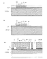
図1は、本発明の実施形態1に係る液体噴射ヘッドの一例であるインクジェット式記録ヘッドの分解斜視図であり、図2は、図1の平面図及びそのA−A′線断面図である。
図1〜図2に示すように、本実施形態の流路形成基板10は、シリコン単結晶基板からなり、その一方の面には二酸化シリコンからなる弾性膜50が形成されている。
(Embodiment 1)
FIG. 1 is an exploded perspective view of an ink jet recording head which is an example of a liquid jet head according to Embodiment 1 of the present invention. FIG. 2 is a plan view of FIG. 1 and a cross-sectional view taken along line AA ′ in FIG. .
As shown in FIGS. 1 to 2, the flow
流路形成基板10には、複数の圧力発生室12がその幅方向に並設されている。また、流路形成基板10の圧力発生室12の長手方向外側の領域には連通部13が形成され、連通部13と各圧力発生室12とが、各圧力発生室12毎に設けられたインク供給路14及び連通路15を介して連通されている。連通部13は、後述する保護基板のマニホールド部31と連通して各圧力発生室12の共通のインク室となるマニホールドの一部を構成する。インク供給路14は、圧力発生室12よりも狭い幅で形成されており、連通部13から圧力発生室12に流入するインクの流路抵抗を一定に保持している。なお、本実施形態では、流路の幅を片側から絞ることでインク供給路14を形成したが、流路の幅を両側から絞ることでインク供給路を形成してもよい。また、流路の幅を絞るのではなく、厚さ方向から絞ることでインク供給路を形成してもよい。本実施形態では、流路形成基板10には、圧力発生室12、連通部13、インク供給路14及び連通路15からなる液体流路が設けられていることになる。
A plurality of
また、流路形成基板10の開口面側には、各圧力発生室12のインク供給路14とは反対側の端部近傍に連通するノズル開口21が穿設されたノズルプレート20が、接着剤や熱溶着フィルム等によって固着されている。なお、ノズルプレート20は、例えば、ガラスセラミックス、シリコン単結晶基板、ステンレス鋼等からなる。
Further, on the opening surface side of the flow
一方、このような流路形成基板10の開口面とは反対側には、上述したように弾性膜50が形成され、この弾性膜50上には、例えば、酸化ジルコニウム(ZrO2)等からなる絶縁体層55が積層形成されている。なお、絶縁体層55上に、必要に応じて、酸化チタン等からなる密着層が設けられていてもよい。
On the other hand, the
また、絶縁体層55上には、第1電極60と、第1電極60の上方に設けられて、厚さが、例えば20〜80nmの配向制御層65と、この配向制御層65上に設けられて厚さが3μm以下、好ましくは0.3〜1.5μmの薄膜である圧電体層70と、圧電体層70の上方に設けられた第2電極80とが、積層形成されて、圧電素子300を構成している。なお、ここで言う上方とは、直上だけでなく、間に他の部材が介在した状態も含むものである。ここで、圧電素子300は、第1電極60、圧電体層70、及び第2電極80、を含む部分をいう。
On the
圧電素子300は、一般的には、何れか一方の電極を共通電極とし、他方の電極をそれぞれ独立する個別電極とする。本実施形態では、圧電素子300の実質的な駆動部となる各圧電体能動部の個別電極として第1電極60を設け、複数の圧電体能動部に共通する共通電極として第2電極80を設けるようにした。ここで、両電極への電圧の印加により圧電歪みが生じる部分を圧電体能動部といい、圧電体能動部から連続するが第1電極60と第2電極80に挟まれておらず、電圧駆動されない部分を圧電体非能動部という。また、圧電素子300と当該圧電素子300の駆動により変位が生じる振動板とを合わせて圧電素子と称するが、アクチュエーター装置とも称する場合がある。
In the
なお、上述した例では、弾性膜50、絶縁体層55、及び第1電極60が圧電素子300と共に変形する振動板として作用するが、勿論これに限定されるものではなく、例えば、弾性膜50及び絶縁体層55を設けずに、第1電極60のみが振動板として作用するようにしてもよい。但し、流路形成基板10上に直接第1電極60を設ける場合には、第1電極60とインクとが導通しないように第1電極60を絶縁性の保護膜等で保護するのが好ましい。
In the above-described example, the
配向制御層65は、ペロブスカイト構造を有し、AサイトがBiを含みBサイトがFe及びTiを含む複合酸化物であり、(100)面に自己配向するものである。具体的には、ABO3型構造のAサイトは酸素が12配位しており、また、Bサイトは酸素が6配位して8面体(オクタヘドロン)をつくっている。配向制御層65を構成する複合酸化物は、基本的には、AサイトのBiと、BサイトのFe及びTiとで構成されるのが好ましい。好ましい組成比は、元素比をBi:Fe:Ti=100:x:(100−x)で表した場合、40≦x≦60となる範囲が好ましい。このような組成比の複合酸化物は、下地に影響されることなく、(100)面に自己配向し、また、この上に成膜されるペロブスカイト構造の圧電材料を(100)面に配向させる配向制御層として機能する。すなわち、詳細は後述するが、配向制御層65は、第1電極60をパターニングした後、成膜されるので、第1電極60上及び絶縁体層55上に成膜されることになるが、何れの下地の上でも(100)面に自己配向し、その後成膜される圧電体層70を(100)面に確実に優先配向させることができ、特に、第1電極60と絶縁体層55との境界近傍においても、圧電体層70の結晶状態の不均一さが低減される。
The
ここで、(100)面に自己配向するとは、下地に影響されることなく、自ら(100)面に配向することをいい、全ての結晶が(100)面に配向している場合と、ほとんどの結晶(例えば、80%以上)が(100)面に配向している場合と、を含むものである。 Here, self-orientation in the (100) plane means that it is oriented in the (100) plane without being affected by the base, and almost all the crystals are oriented in the (100) plane. In which the crystal (for example, 80% or more) is oriented in the (100) plane.
なお、このような機能が阻害されない範囲で、AサイトやBサイトの元素の一部を他の元素で置換した複合酸化物としてもよく、これも本発明の配向制御層に包含される。例えば、AサイトにBiの他にBa、Sr、Laなどの元素がさらに存在してもよいし、BサイトにFe及びTiと共にZr、Nbなどの元素がさらに存在していてもよい。また、上述した機能を有する限り、元素(Bi、Fe、Ti、O)の欠損や過剰により化学量論の組成(ABO3)からずれたものも、本発明の配向制御層に包含される。例えば、Biが化学量論比より過剰に含有される複合酸化物も(100)面に自己配向し、配向制御層として機能することが後述するように確認されている。 In addition, as long as such a function is not hindered, a composite oxide in which a part of the elements at the A site and the B site is substituted with other elements may be included in the alignment control layer of the present invention. For example, in addition to Bi, elements such as Ba, Sr, and La may further exist at the A site, and elements such as Zr and Nb may also exist along with Fe and Ti at the B site. In addition, as long as it has the above-described function, those that deviate from the stoichiometric composition (ABO 3 ) due to deficiency or excess of the elements (Bi, Fe, Ti, O) are also included in the orientation control layer of the present invention. For example, it has been confirmed that a composite oxide containing Bi in excess of the stoichiometric ratio is self-oriented in the (100) plane and functions as an orientation control layer, as will be described later.
なお、配向制御層65は、後述する圧電体層70を形成する圧電材料と同様なペロブスカイト構造を有して、小さいが圧電特性を有するものであり、配向制御層65と圧電体層70とを併せて圧電体層ということもできる。
The
圧電体層70は、ペロブスカイト構造、すなわちABO3型構造を有する複合酸化物からなる圧電材料である。なお、ペロブスカイト構造は、Aサイトは酸素が12配位しており、また、Bサイトは酸素が6配位して8面体(オクタヘドロン)をつくっている構造である。このような圧電材料としては、例えば、チタン酸ジルコン酸鉛(PZT)や、これに酸化ニオブ、酸化ニッケル又は酸化マグネシウム等の金属酸化物を添加したもの等を挙げることができる。具体的には、チタン酸鉛(PbTiO3)、チタン酸ジルコン酸鉛(Pb(Zr,Ti)O3)、ジルコニウム酸鉛(PbZrO3)、チタン酸鉛ランタン((Pb,La),TiO3)、ジルコン酸チタン酸鉛ランタン((Pb,La)(Zr,Ti)O3)又は、マグネシウムニオブ酸ジルコニウムチタン酸鉛(Pb(Zr,Ti)(Mg,Nb)O3)等を用いることができる。
The
また、圧電体層70の材料としては、鉛を含む鉛系の圧電材料に限定されず、鉛を含まない非鉛系のペロブス構造を有する圧電材料を用いることもできる。非鉛系の圧電材料としては、例えば、鉄酸ビスマス((BiFeO3)、略「BFO」)、チタン酸バリウム((BaTiO3)、略「BT」)、ニオブ酸カリウムナトリウム((K,Na)(NbO3)、略「KNN」)、ニオブ酸カリウムナトリウムリチウム((K,Na,Li)(NbO3))、ニオブ酸タンタル酸カリウムナトリウムリチウム((K,Na,Li)(Nb,Ta)O3)、チタン酸ビスマスカリウム((Bi1/2K1/2)TiO3、略「BKT」)、チタン酸ビスマスナトリウム((Bi1/2Na1/2)TiO3、略「BNT」)、マンガン酸ビスマス(BiMnO3、略「BM」)、ビスマス、カリウム、チタン及び鉄を含みペロブスカイト構造を有する複合酸化物(x[(BixK1−x)TiO3]−(1−x)[BiFeO3]、略「BKT−BF」)、ビスマス、鉄、バリウム及びチタンを含みペロブスカイト構造を有する複合酸化物((1−x)[BiFeO3]−x[BaTiO3]、略「BFO−BT」)や、これにマンガン、コバルト、クロムなどの金属を添加したもの((1−x)[Bi(Fe1−yMy)O3]−x[BaTiO3](Mは、Mn、CoまたはCr))等が挙げられる。
In addition, the material of the
このようなペロブスカイト構造の圧電材料は、配向制御層65上に成膜されることにより、配向制御層65の結晶配向を受け継ぎ、(100)面に優先配向する。ここで、優先配向するとは、本発明では、XRDの(100)面に由来するピーク強度を(110)面に由来するピーク強度とを比較してした際に、(100)/[(100)+(110)]が60%以上、好ましくは、70%以上であることをいう。勿論、(100)面のピークの割合が大きい方が圧電体層70の変位特性及び耐久性の向上の面では好ましく、(100)/[(100)+(110)]が80%以上が好ましく、(100)/[(100)+(110)]が90%以上がさらに好ましい。なお、後述する実施例においては、(100)/[(100)+(110)]が90%以上となることが確認されている。なお、圧電材料は、(100)面に優先配向して変位特性が優れたものとなるという観点から、菱面体晶であるのが好ましい。
The piezoelectric material having such a perovskite structure is formed on the
第2電極80としては、Ir,Pt,タングステン(W),タンタル(Ta),モリブデン(Mo)等の各種金属の何れでもよく、また、これらの合金や、酸化イリジウム等の金属酸化物が挙げられる。
The
このような各圧電素子300の第2電極80には、インク供給路14側の端部近傍から引き出され、流路形成基板10の絶縁体層55上に延設された金(Au)等のリード電極90がそれぞれ接続されている。このリード電極90を介して各圧電素子300に選択的に電圧が印加される。
The
このような圧電素子300が形成された流路形成基板10上、すなわち、第1電極60、弾性膜50及びリード電極90上には、マニホールド100の少なくとも一部を構成するマニホールド部31を有する保護基板30が接着剤35を介して接合されている。このマニホールド部31は、本実施形態では、保護基板30を厚さ方向に貫通して圧力発生室12の幅方向に亘って形成されており、上述のように流路形成基板10の連通部13と連通されて各圧力発生室12の共通のインク室となるマニホールド100を構成している。
On the flow
また、保護基板30の圧電素子300に対向する領域には、圧電素子300の運動を阻害しない程度の空間を有する圧電素子保持部32が設けられている。圧電素子保持部32は、圧電素子300の運動を阻害しない程度の空間を有していればよく、当該空間は密封されていても、密封されていなくてもよい。
A piezoelectric
このような保護基板30としては、流路形成基板10の熱膨張率と略同一の材料、例えば、ガラス、セラミック材料等を用いることが好ましく、本実施形態では、流路形成基板10と同一材料のシリコン単結晶基板を用いて形成した。
As such a
また、保護基板30には、保護基板30を厚さ方向に貫通する貫通孔33が設けられている。そして、各圧電素子300から引き出されたリード電極90の端部近傍は、貫通孔33内に露出するように設けられている。
The
また、保護基板30上には、並設された圧電素子300を駆動するための駆動回路120が固定されている。この駆動回路120としては、例えば、回路基板や半導体集積回路(IC)等を用いることができる。そして、駆動回路120とリード電極90とは、ボンディングワイヤー等の導電性ワイヤーからなる接続配線121を介して電気的に接続されている。
A
また、このような保護基板30上には、封止膜41及び固定板42とからなるコンプライアンス基板40が接合されている。ここで、封止膜41は、剛性が低く可撓性を有する材料(例えば、厚さが6μmのポリフェニレンサルファイド(PPS)フィルム)からなり、この封止膜41によってマニホールド部31の一方面が封止されている。また、固定板42は、金属等の硬質の材料(例えば、厚さが30μmのステンレス鋼(SUS)等)で形成される。この固定板42のマニホールド100に対向する領域は、厚さ方向に完全に除去された開口部43となっているため、マニホールド100の一方面は可撓性を有する封止膜41のみで封止されている。
In addition, a
このような本実施形態のインクジェット式記録ヘッドでは、図示しない外部インク供給手段と接続したインク導入口からインクを取り込み、マニホールド100からノズル開口21に至るまで内部をインクで満たした後、駆動回路120からの記録信号に従い、圧力発生室12に対応するそれぞれの第1電極60と第2電極80との間に電圧を印加し、弾性膜50、絶縁体層55、第1電極60及び圧電体層70をたわみ変形させることにより、各圧力発生室12内の圧力が高まりノズル開口21からインク滴が吐出する。
In such an ink jet recording head of the present embodiment, ink is taken in from an ink introduction port connected to an external ink supply means (not shown), and the interior from the manifold 100 to the
次に、本実施形態のインクジェット式記録ヘッドの製造方法の一例について、図3〜図6を参照して説明する。なお、図3〜図6は、圧力発生室の長手方向(第2方向)の断面図である。 Next, an example of a method for manufacturing the ink jet recording head of this embodiment will be described with reference to FIGS. 3 to 6 are cross-sectional views in the longitudinal direction (second direction) of the pressure generating chamber.
まず、図3(a)に示すように、シリコンウェハーである流路形成基板用ウェハーの表面に弾性膜50を構成する二酸化シリコン(SiO2)等からなる二酸化シリコン膜を形成する。次いで、図3(b)に示すように、弾性膜50(二酸化シリコン膜)上に、酸化ジルコニウム等からなる絶縁体層55を形成する。
First, as shown in FIG. 3A, a silicon dioxide film made of silicon dioxide (SiO 2 ) or the like that constitutes the
次に、図4(a)に示すように、絶縁体層55上に、白金からなる第1電極60をスパッタリング法や蒸着法等により全面に形成する。次いで、図4(b)に示すように、第1電極60上に所定形状のレジスト(図示無し)をマスクとして、第1電極60をパターニングする。
Next, as shown in FIG. 4A, a
次に、図4(c)に示すように、レジストを剥離した後、第1電極60上(及び絶縁体層55)に、AサイトがBiを含みBサイトがFe及びTiを含むペロブスカイト構造を有する複合酸化物となる前駆体である配向制御層前駆体層66を形成し、これを焼成することにより、ペロブスカイト構造を有する複合酸化物からなる配向制御層65とする(図4(d))。このように配向制御層65は、例えば、金属錯体を含む前駆体溶液を塗布して配向制御層前駆体層66を形成し、これを乾燥し、さらに高温で焼成することで金属酸化物からなる配向制御層65を得る、MOD(Metal−Organic Decomposition)法やゾル−ゲル法等の化学溶液法を用いて製造できる。その他、レーザーアブレーション法、スパッタリング法、パルス・レーザー・デポジション法(PLD法)、CVD法、エアロゾル・デポジション法などでも、配向制御層65を製造することができる。
Next, as shown in FIG. 4C, after removing the resist, a perovskite structure in which the A site contains Bi and the B site contains Fe and Ti is formed on the first electrode 60 (and the insulator layer 55). An alignment control
配向制御層65を化学溶液法で形成する場合の具体的な形成手順例としては、まず、図4(c)に示すように、Bi、Fe、Tiを含有する金属錯体を含むMOD溶液やゾルからなる配向制御層形成用組成物(配向制御層の前駆体溶液)をスピンコート法などを用いて、塗布して配向制御層前駆体層66を形成する(配向制御層前駆体溶液塗布工程)。
As a specific example of the formation procedure when the
塗布するバッファー層の前駆体溶液は、焼成によりAサイトがBiを含みBサイトがFe及びTiを含むペロブスカイト構造を有する複合酸化物を形成しうる金属錯体を混合し、該混合物を有機溶媒に溶解または分散させたものである。Biや、Fe、Ti等をそれぞれ含む金属錯体としては、例えば、アルコキシド、有機酸塩、βジケトン錯体などを用いることができる。Biを含む金属錯体としては、例えば2−エチルヘキサン酸ビスマス、酢酸ビスマスなどが挙げられる。Feを含む金属錯体としては、例えば2−エチルヘキサン酸鉄、酢酸鉄、トリス(アセチルアセトナート)鉄などが挙げられる。Tiを含む金属錯体としては、例えば2−エチルヘキサン酸チタン、酢酸チタンなどが挙げられる。また、配向制御層の前駆体溶液の溶媒としては、プロパノール、ブタノール、ペンタノール、ヘキサノール、オクタノール、エチレングリコール、プロピレングリコール、オクタン、デカン、シクロヘキサン、キシレン、トルエン、テトラヒドロフラン、酢酸、オクチル酸などが挙げられる。 The precursor solution of the buffer layer to be applied is mixed with a metal complex capable of forming a composite oxide having a perovskite structure in which the A site contains Bi and the B site contains Fe and Ti by firing, and the mixture is dissolved in an organic solvent. Or they are dispersed. As a metal complex containing Bi, Fe, Ti, or the like, for example, an alkoxide, an organic acid salt, a β-diketone complex, or the like can be used. Examples of the metal complex containing Bi include bismuth 2-ethylhexanoate and bismuth acetate. Examples of the metal complex containing Fe include iron 2-ethylhexanoate, iron acetate, and tris (acetylacetonato) iron. Examples of the metal complex containing Ti include titanium 2-ethylhexanoate and titanium acetate. Examples of the solvent for the precursor solution of the orientation control layer include propanol, butanol, pentanol, hexanol, octanol, ethylene glycol, propylene glycol, octane, decane, cyclohexane, xylene, toluene, tetrahydrofuran, acetic acid, octylic acid, and the like. It is done.
次いで、この配向制御層前駆体層66を所定温度(例えば、150〜200℃)に加熱して一定時間乾燥させる(配向制御層乾燥工程)。次に、乾燥した配向制御層前駆体層66を所定温度(例えば、350〜450℃)に加熱して一定時間保持することによって脱脂する(配向制御層脱脂工程)。ここで言う脱脂とは、配向制御層前駆体層66に含まれる有機成分を、例えば、NO2、CO2、H2O等として離脱させることである。配向制御層乾燥工程や配向制御層脱脂工程の雰囲気は限定されず、大気中、酸素雰囲気中や、不活性ガス中でもよい。
Next, the orientation control
次に、図4(d)に示すように、配向制御層前駆体層66を所定温度、例えば600〜850℃程度に加熱して、一定時間、例えば、1〜10分間保持することによって結晶化させ、AサイトがBiを含みBサイトがFe及びTiを含むペロブスカイト構造を有する複合酸化物からなる配向制御層65を形成する(焼成工程)。
Next, as shown in FIG. 4D, the orientation control
この配向制御層焼成工程においても、雰囲気は限定されず、大気中、酸素雰囲気中や、不活性ガス中でもよい。配向制御層乾燥工程、配向制御層脱脂工程及び配向制御層焼成工程で用いられる加熱装置としては、例えば、赤外線ランプの照射により加熱するRTA(Rapid Thermal Annealing)装置やホットプレート等が挙げられる。 Also in this orientation control layer firing step, the atmosphere is not limited, and it may be in the air, in an oxygen atmosphere, or in an inert gas. Examples of the heating device used in the orientation control layer drying step, the orientation control layer degreasing step, and the orientation control layer firing step include an RTA (Rapid Thermal Annealing) device that heats by irradiation with an infrared lamp and a hot plate.
本実施形態では、塗布工程を1回として1層からなる配向制御層65を形成したが、上述した配向制御層塗布工程、配向制御層乾燥工程及び配向制御層脱脂工程や、配向制御層塗布工程、配向制御層乾燥工程、配向制御層脱脂工程及び配向制御層焼成工程を所望の膜厚等に応じて複数回繰り返して複数層からなる配向制御層65を形成してもよい。但し、圧電体膜72の変位特性を低減させないためには薄い方が好ましく、厚さ20nm〜80nm、好ましくは、20〜50nmとするのが好ましい。
In this embodiment, the
次に、配向制御層65上にペロブスカイト構造を有する複合酸化物からなる圧電体層70を形成する。圧電体層70は、例えば、金属錯体を含む溶液を塗布乾燥し、脱脂することにより製造することができる。その他、レーザーアブレーション法、スパッタリング法、パルス・レーザー・デポジション法(PLD法)、CVD法、エアロゾル・デポジション法などでも圧電体層70を製造することもできる。
Next, a
例えば、まず、図5(a)に示すように、配向制御層65上に、圧電体層70となる圧電材料の構成金属を含有する有機金属錯体を含むゾルやMOD溶液(前駆体溶液)を、スピンコート法などを用いて、塗布して圧電体前駆体膜71を形成する(塗布工程)。
For example, first, as shown in FIG. 5A, a sol or MOD solution (precursor solution) containing an organometallic complex containing a constituent metal of a piezoelectric material to be the
塗布する前駆体溶液は、例えば、圧電体層70となる圧電材料の構成金属をそれぞれ含む有機金属錯体を、各構成金属が所望のモル比となるように混合し、該混合物をアルコールなどの有機溶媒を用いて溶解または分散させたものである。圧電材料の構成金属を含む有機金属錯体としては、例えば、金属アルコキシド、有機酸塩、βジケトン錯体などを用いることができる。具体的には、例えば、以下のものが挙げられる。鉛(Pb)を含む有機金属錯体としては、例えば酢酸鉛などが挙げられる。ジルコニウム(Zr)を含む有機金属錯体としては、例えばジルコニウムアセチルアセトナート、ジルコニウムテトラアセチルアセトナート、ジルコニウムモノアセチルアセトナート、ジルコニウムビスアセチルアセトナート等が挙げられる。チタニウム(Ti)を含む有機金属錯体としては、例えばチタニウムアルコキシド、チタニウムイソプロポキシド等が挙げられる。
The precursor solution to be applied is prepared by, for example, mixing organometallic complexes each containing a constituent metal of the piezoelectric material that becomes the
次いで、この圧電体前駆体膜71を所定温度、例えば130℃〜180℃程度に加熱して一定時間乾燥させる(乾燥工程)。次に、乾燥した圧電体前駆体膜71を所定温度、例えば300℃〜400℃に加熱して一定時間保持することによって脱脂する(脱脂工程)。なお、ここで言う脱脂とは、圧電体前駆体膜71に含まれる有機成分を、例えば、NO2、CO2、H2O等として離脱させることである。
Next, the
次に、図5(b)に示すように、圧電体前駆体膜71を所定温度、例えば650〜800℃程度に加熱して一定時間保持することによって結晶化させ、圧電体膜72を形成する(焼成工程)。乾燥工程、脱脂工程及び焼成工程で用いられる加熱装置としては、例えば、赤外線ランプの照射により加熱するRTA(Rapid Thermal Annealing)装置やホットプレート等が挙げられる。
Next, as shown in FIG. 5B, the
なお、上述した塗布工程、乾燥工程及び脱脂工程や、塗布工程、乾燥工程、脱脂工程及び焼成工程を所望の膜厚等に応じて複数回繰り返すことにより、複数層の圧電体膜からなる圧電体層を形成してもよい。 In addition, by repeating the coating process, the drying process and the degreasing process described above, the coating process, the drying process, the degreasing process, and the firing process a plurality of times according to a desired film thickness, etc., a piezoelectric body composed of a plurality of layers of piezoelectric films. A layer may be formed.
次いで、上述した塗布工程、乾燥工程及び脱脂工程や、塗布工程、乾燥工程、脱脂工程及び焼成工程を所望の膜厚等に応じて複数回繰り返して複数の圧電体膜72からなる圧電体層70を形成することで、図5(c)に示すように複数層の圧電体膜72からなる所定厚さの圧電体層70を形成する。例えば、塗布溶液の1回あたりの膜厚が0.1μm程度の場合には、例えば、10層の圧電体膜72からなる圧電体層70全体の膜厚は約1.1μm程度となる。なお、本実施形態では、圧電体膜72を積層して設けたが、1層のみでもよい。
Next, the above-described coating process, drying process, degreasing process, coating process, drying process, degreasing process, and firing process are repeated a plurality of times in accordance with a desired film thickness and the like, and the
上述したように、所定のAサイトがBiを含みBサイトがFe及びTiを含むペロブスカイト構造を有する複合酸化物からなる配向制御層65上に圧電体層70を形成することにより、配向制御層65により圧電体層70の配向が制御され、(100)面に優先配向した圧電体層70とすることができる。
As described above, the
圧電体層70を形成した後は、図6(a)に示すように、圧電体層70上に、例えば、白金等の金属からなる第2電極80を積層し、圧電体層70及び第2電極80を同時にパターニングして圧電素子300を形成する。なお、圧電体層70と第2電極80とのパターニングでは、所定形状に形成したレジスト(図示なし)を介してドライエッチングすることにより一括して行うことができる。その後、必要に応じて、600℃〜800℃の温度域でポストアニールを行ってもよい。これにより、圧電体層70と第1電極60や第2電極80との良好な界面を形成することができ、かつ、圧電体層70の結晶性を改善することができる。
After the
次に、図6(b)に示すように、流路形成基板用ウェハー110の全面に亘って、例えば、金(Au)等からなるリード電極90を形成後、例えば、レジスト等からなるマスクパターン(図示なし)を介して各圧電素子300毎にパターニングする。
Next, as shown in FIG. 6B, a
次に、図6(c)に示すように、流路形成基板用ウェハー110の圧電素子300側に、シリコンウェハーであり複数の保護基板30となる保護基板用ウェハー130を接着剤35を介して接合した後に、流路形成基板用ウェハー110を所定の厚さに薄くする。
Next, as shown in FIG. 6C, a
次に、図示しないが、流路形成基板用ウェハー110上に、マスク膜を新たに形成し、所定形状にパターニングする。そして、流路形成基板用ウェハー110をマスク膜を介してKOH等のアルカリ溶液を用いた異方性エッチング(ウェットエッチング)することにより、圧電素子300に対応する圧力発生室12、連通部13、インク供給路14及び連通路15等を形成する。
Next, although not shown, a mask film is newly formed on the flow path forming
その後は、流路形成基板用ウェハー110及び保護基板用ウェハー130の外周縁部の不要部分を、例えば、ダイシング等により切断することによって除去する。そして、流路形成基板用ウェハー110の保護基板用ウェハー130とは反対側の面のマスク膜を除去した後にノズル開口21が穿設されたノズルプレート20を接合すると共に、保護基板用ウェハー130にコンプライアンス基板40を接合し、流路形成基板用ウェハー110等を図1に示すような一つのチップサイズの流路形成基板10等に分割することによって、本実施形態のインクジェット式記録ヘッドIとする。
Thereafter, unnecessary portions of the outer peripheral edge portions of the flow path forming
本実施形態では、AサイトがBiを含みBサイトがFe及びTiを含むペロブスカイト構造を有する複合酸化物からなる配向制御層65上に、圧電体層70を形成することにより、下地に影響されることなく、すなわち、下地が第1電極60の領域も絶縁体層55の領域も同様に(100)面に優先配向した圧電体層70を形成することができる。
In this embodiment, the base layer is affected by forming the
以下、実施例を示し、本発明をさらに具体的に説明する。なお、本発明は以下の実施例に限定されるものではない。 Hereinafter, the present invention will be described more specifically with reference to examples. In addition, this invention is not limited to a following example.
(実施例1)
<基板の準備>
まず、(110)に配向した単結晶シリコン基板の表面に熱酸化により膜厚1170nmの二酸化シリコン膜を形成した。次に、二酸化シリコン膜上にRFマグネトロンスパッター法により膜厚20nmのチタン膜を形成し、熱酸化することで酸化チタン膜を形成した。次に、酸化チタン膜上にRFマグネトロンスパッター法により膜厚130nmの白金膜からなる第1電極60を形成して電極付き基板とした。
Example 1
<Preparation of substrate>
First, a silicon dioxide film having a thickness of 1170 nm was formed by thermal oxidation on the surface of a single crystal silicon substrate oriented in (110). Next, a titanium film with a thickness of 20 nm was formed on the silicon dioxide film by RF magnetron sputtering, and a titanium oxide film was formed by thermal oxidation. Next, a
<配向制御層>
2−エチルヘキサン酸ビスマス、2−エチルヘキサン酸鉄、2−エチルヘキサン酸チタンの各n−オクタン溶液を混合し、Bi:Fe:Tiのモル比が、100:40:60となる割合で混合して、配向制御層前駆体溶液を調製した。
<Orientation control layer>
Each n-octane solution of bismuth 2-ethylhexanoate, iron 2-ethylhexanoate, and titanium 2-ethylhexanoate is mixed and mixed at a ratio of Bi: Fe: Ti of 100: 40: 60. Thus, an alignment control layer precursor solution was prepared.
この配向制御層前駆体溶液を上記電極付き基板上にスピンコーターで成膜した後、ホットプレート上で180℃×3min、350℃×3minでベークし、アモルファス膜を形成する。次いで、ランプアニール炉を用いて700℃×5min焼成し、厚さ80nmの配向制御層とした。 The orientation control layer precursor solution is formed on the substrate with electrodes by a spin coater and then baked on a hot plate at 180 ° C. × 3 min and 350 ° C. × 3 min to form an amorphous film. Next, firing was performed at 700 ° C. for 5 minutes using a lamp annealing furnace to obtain an orientation control layer having a thickness of 80 nm.
<圧電体層>
Bi、Ba、Fe、Mn及びTiを含みペロブスカイト構造を有する複合酸化物からなる圧電体層を形成するために、2−エチルヘキサン酸ビスマス、2−エチルヘキサン酸バリウム、2−エチルヘキサン酸鉄、2−エチルヘキサン酸マンガン、2−エチルヘキサン酸チタンの各n−オクタン溶液を混合し、Bi:Ba:Fe:Mn:Tiのモル比が、Bi:Ba:Fe:Mn:Ti=75.0:25.0:71.3:3.8:25.0となるように混合して、BFM−BTからなる圧電体層の前駆体溶液を調製した。
<Piezoelectric layer>
In order to form a piezoelectric layer made of a composite oxide containing Bi, Ba, Fe, Mn and Ti and having a perovskite structure, bismuth 2-ethylhexanoate, barium 2-ethylhexanoate, iron 2-ethylhexanoate, Each n-octane solution of manganese 2-ethylhexanoate and titanium 2-ethylhexanoate was mixed, and the molar ratio of Bi: Ba: Fe: Mn: Ti was Bi: Ba: Fe: Mn: Ti = 75.0. : 25.0: 71.3: 3.8: 25.0 to prepare a piezoelectric layer precursor solution of BFM-BT.
圧電体層前駆体溶液を適量マイクロピペットに取り、スピンコータにセットした基板の配向制御層上に滴下する。スピンコータで成膜した後、ホットプレート上で180℃×3min、350℃×3minでベークしアモルファス膜を形成する。ランプアニール炉を用いて750℃×5min焼成し、第1の圧電体膜をとした。 An appropriate amount of the piezoelectric layer precursor solution is taken into a micropipette and dropped onto the orientation control layer of the substrate set on the spin coater. After forming a film with a spin coater, an amorphous film is formed by baking on a hot plate at 180 ° C. × 3 min and 350 ° C. × 3 min. The first piezoelectric film was obtained by firing at 750 ° C. for 5 minutes using a lamp annealing furnace.
同様にさらに圧電体膜を作製するため、圧電体層前駆体溶液を適量マイクロピペットに取り、スピンコータにセットした基板上に滴下する。スピンコータで成膜した後、ホットプレート上で180℃×3min、350℃×3minでベークしてアモルファス膜を形成する。この作業を2回繰り返した後、ランプアニール炉を用いて750℃×5min焼成して結晶膜とした。ランプアニール炉までの工程を5回繰り返し、11層の圧電体膜からなる、厚さ900nmの圧電体層を形成した。この圧電体層上にスパッタリング法を用いてイリジウムからなる第2電極を形成した。 Similarly, in order to further produce a piezoelectric film, an appropriate amount of the piezoelectric layer precursor solution is taken into a micropipette and dropped onto a substrate set on a spin coater. After film formation with a spin coater, an amorphous film is formed by baking on a hot plate at 180 ° C. × 3 min and 350 ° C. × 3 min. After repeating this operation twice, it was baked at 750 ° C. for 5 minutes using a lamp annealing furnace to obtain a crystal film. The process up to the lamp annealing furnace was repeated five times to form a 900 nm-thick piezoelectric layer composed of 11 layers of piezoelectric films. A second electrode made of iridium was formed on the piezoelectric layer by sputtering.
(実施例2)
Bi:Fe:Tiのモル比が、100:50:50となる配向制御層前駆体溶液を用いた以外は、実施例1と同様にした。
(Example 2)
The same procedure as in Example 1 was performed except that the orientation control layer precursor solution having a Bi: Fe: Ti molar ratio of 100: 50: 50 was used.
(実施例3)
Bi:Fe:Tiのモル比が、100:60:40となる配向制御層前駆体溶液を用いた以外は、実施例1と同様にした。
Example 3
The same procedure as in Example 1 was performed except that the orientation control layer precursor solution having a Bi: Fe: Ti molar ratio of 100: 60: 40 was used.
(実施例4)
Bi:Fe:Tiのモル比が、100:50:50となる配向制御層前駆体溶液を用い、配向制御層の膜厚を60nmとした以外は、実施例1と同様にした。
Example 4
The same procedure as in Example 1 was carried out except that an orientation control layer precursor solution having a Bi: Fe: Ti molar ratio of 100: 50: 50 was used and the thickness of the orientation control layer was changed to 60 nm.
(実施例5)
Bi:Fe:Tiのモル比が、100:50:50となる配向制御層前駆体溶液を用い、配向制御層の膜厚を40nmとした以外は、実施例1と同様にした。
(Example 5)
The same procedure as in Example 1 was conducted, except that an orientation control layer precursor solution having a Bi: Fe: Ti molar ratio of 100: 50: 50 was used and the thickness of the orientation control layer was 40 nm.
(実施例6)
Bi:Fe:Tiのモル比が、100:50:50となる配向制御層前駆体溶液を用い、配向制御層の膜厚を30nmとした以外は、実施例1と同様にした。
(Example 6)
The same procedure as in Example 1 was conducted, except that an orientation control layer precursor solution having a Bi: Fe: Ti molar ratio of 100: 50: 50 was used and the thickness of the orientation control layer was changed to 30 nm.
(実施例7)
Bi:Fe:Tiのモル比が、100:50:50となる配向制御層前駆体溶液を用い、配向制御層の膜厚を20nmとした以外は、実施例1と同様にした。
(Example 7)
The same procedure as in Example 1 was carried out except that an orientation control layer precursor solution having a Bi: Fe: Ti molar ratio of 100: 50: 50 was used and the thickness of the orientation control layer was 20 nm.
(実施例8)
Bi:Fe:Tiのモル比が、105:50:50となる配向制御層前駆体溶液を用い、配向制御層の膜厚を40nmとした以外は、実施例1と同様にした。
(Example 8)
The same procedure as in Example 1 was carried out except that an orientation control layer precursor solution having a Bi: Fe: Ti molar ratio of 105: 50: 50 was used and the thickness of the orientation control layer was 40 nm.
(実施例9)
Bi:Fe:Tiのモル比が、110:50:50となる配向制御層前駆体溶液を用い、配向制御層の膜厚を40nmとした以外は、実施例1と同様にした。
Example 9
The same procedure as in Example 1 was conducted, except that an orientation control layer precursor solution having a Bi: Fe: Ti molar ratio of 110: 50: 50 was used and the thickness of the orientation control layer was 40 nm.
(実施例10)
Bi:Fe:Tiのモル比が、115:50:50となる配向制御層前駆体溶液を用い、配向制御層の膜厚を40nmとした以外は、実施例1と同様にした。
(Example 10)
The same procedure as in Example 1 was conducted, except that an orientation control layer precursor solution having a Bi: Fe: Ti molar ratio of 115: 50: 50 was used and the thickness of the orientation control layer was 40 nm.
(実施例11)
Bi:Fe:Tiのモル比が、105:50:50となる配向制御層前駆体溶液を用い、配向制御層の膜厚を20nmとした以外は、実施例1と同様にした。
(Example 11)
The same procedure as in Example 1 was carried out except that an orientation control layer precursor solution having a Bi: Fe: Ti molar ratio of 105: 50: 50 was used and the thickness of the orientation control layer was 20 nm.
(実施例12)
Bi:Fe:Tiのモル比が、110:50:50となる配向制御層前駆体溶液を用い、配向制御層の膜厚を20nmとした以外は、実施例1と同様にした。
(Example 12)
The same procedure as in Example 1 was conducted, except that an orientation control layer precursor solution having a Bi: Fe: Ti molar ratio of 110: 50: 50 was used and the thickness of the orientation control layer was 20 nm.
(実施例13)
Bi:Fe:Tiのモル比が、115:50:50となる配向制御層前駆体溶液を用い、配向制御層の膜厚を20nmとした以外は、実施例1と同様にした。
(Example 13)
The same procedure as in Example 1 was conducted, except that an orientation control layer precursor solution having a Bi: Fe: Ti molar ratio of 115: 50: 50 was used and the thickness of the orientation control layer was 20 nm.
(実施例14)
第1電極をIr電極とした電極付き基板を用い、Bi:Fe:Tiのモル比が、115:50:50となる配向制御層前駆体溶液を用い、配向制御層の膜厚を60nmとした以外は、実施例1と同様にした。
(Example 14)
A substrate with an electrode having the first electrode as an Ir electrode was used, an alignment control layer precursor solution having a Bi: Fe: Ti molar ratio of 115: 50: 50 was used, and the thickness of the alignment control layer was set to 60 nm. Except for this, the procedure was the same as in Example 1.
(実施例15)
第1電極をIr電極とした電極付き基板を用い、Bi:Fe:Tiのモル比が、115:50:50となる配向制御層前駆体溶液を用い、配向制御層の膜厚を40nmとした以外は、実施例1と同様にした。
(Example 15)
A substrate with an electrode having an Ir electrode as the first electrode was used, an orientation control layer precursor solution having a Bi: Fe: Ti molar ratio of 115: 50: 50 was used, and the thickness of the orientation control layer was 40 nm. Except for this, the procedure was the same as in Example 1.
(実施例16)
第1電極をIr電極とした電極付き基板を用い、Bi:Fe:Tiのモル比が、115:50:50となる配向制御層前駆体溶液を用い、配向制御層の膜厚を30nmとした以外は、実施例1と同様にした。
(Example 16)
A substrate with an electrode having the first electrode as an Ir electrode was used, an alignment control layer precursor solution having a Bi: Fe: Ti molar ratio of 115: 50: 50 was used, and the thickness of the alignment control layer was set to 30 nm. Except for this, the procedure was the same as in Example 1.
(実施例17)
第1電極及び第2電極を設けないで、酸化シリコン膜及び酸化ジルコニウムからなる絶縁体層の基板を用い、Bi:Fe:Tiのモル比が、100:50:50となる配向制御層前駆体溶液を用い、配向制御層の膜厚を40nmとした以外は、実施例1と同様にした。
(Example 17)
Without using the first electrode and the second electrode, a substrate of an insulator layer made of a silicon oxide film and zirconium oxide is used, and a Bi: Fe: Ti molar ratio is 100: 50: 50. The same procedure as in Example 1 was performed except that the solution was used and the thickness of the orientation control layer was changed to 40 nm.
(実施例18)
第1電極及び第2電極を設けないで、酸化シリコン膜及び酸化ジルコニウムからなる絶縁体層を基板を用い、Bi:Fe:Tiのモル比が、115:50:50となる配向制御層前駆体溶液を用い、配向制御層の膜厚を80nmとした以外は、実施例1と同様にした。
(Example 18)
Without providing the first electrode and the second electrode, the substrate is an insulator layer made of a silicon oxide film and zirconium oxide, and the Bi: Fe: Ti molar ratio is 115: 50: 50. The same procedure as in Example 1 was performed except that the solution was used and the film thickness of the orientation control layer was changed to 80 nm.
(実施例19)
Bi:Fe:Tiのモル比が、115:50:50となる配向制御層前駆体溶液を用い、配向制御層の膜厚を60nmとした以外は、実施例1と同様にした。
(Example 19)
The same procedure as in Example 1 was carried out except that an orientation control layer precursor solution having a Bi: Fe: Ti molar ratio of 115: 50: 50 was used and the thickness of the orientation control layer was changed to 60 nm.
(実施例20)
Bi:Fe:Tiのモル比が、115:50:50となる配向制御層前駆体溶液を用い、配向制御層の膜厚を40nmとした以外は、実施例1と同様にした。
(Example 20)
The same procedure as in Example 1 was conducted, except that an orientation control layer precursor solution having a Bi: Fe: Ti molar ratio of 115: 50: 50 was used and the thickness of the orientation control layer was 40 nm.
(実施例21)
Bi:Fe:Tiのモル比が、115:50:50となる配向制御層前駆体溶液を用い、配向制御層の膜厚を20nmとした以外は、実施例1と同様にした。
(Example 21)
The same procedure as in Example 1 was conducted, except that an orientation control layer precursor solution having a Bi: Fe: Ti molar ratio of 115: 50: 50 was used and the thickness of the orientation control layer was 20 nm.
(実施例22)
まず、酢酸鉛3水和物(Pb(CH3COO)2・3H2O)、チタニウムイソプロポキシド(Ti[OCH(CH3)2]4)、ジルコニウムアセチルアセトナート(Zr(CH3COCHCOCH3)4)を主原料とし、ブチルセロソルブ(C6H14O6)を溶媒とし、ジエタノールアミン(C4H11NO2)を安定剤とし、ポリエチレングリコール(C2H6O6)を増粘剤として混合したPZT前駆体溶液を得た。なお、前駆体溶液は、酢酸鉛3水和物:チタニウムイソプロポキシド:ジルコニウムアセチルアセトナート:ブチルセロソルブ:ジエタノールアミン:ポリエチレングリコール=1.1:0.44:0.56:3:0.65:0.5(モル比)の割合で混合した。また、酢酸鉛3水和物は蒸発による減少を考慮して10%過剰に加えている。
(Example 22)
First, lead acetate trihydrate (Pb (CH 3 COO) 2 .3H 2 O), titanium isopropoxide (Ti [OCH (CH 3 ) 2 ] 4 ), zirconium acetylacetonate (Zr (CH 3 COCHCOCH 3 4 ) as a main raw material, butyl cellosolve (C 6 H 14 O 6 ) as a solvent, diethanolamine (C 4 H 11 NO 2 ) as a stabilizer, and polyethylene glycol (C 2 H 6 O 6 ) as a thickener A mixed PZT precursor solution was obtained. The precursor solution was lead acetate trihydrate: titanium isopropoxide: zirconium acetylacetonate: butyl cellosolve: diethanolamine: polyethylene glycol = 1.1: 0.44: 0.56: 3: 0.65: 0 .5 (molar ratio). Further, lead acetate trihydrate is added in excess of 10% in consideration of the decrease due to evaporation.
Bi:Fe:Tiのモル比が、100:50:50となる配向制御層前駆体溶液を用い、配向制御層の膜厚を60nmと、さらにPZT前駆体溶液を用いて厚さ900nmとした以外は、実施例1と同様にした。 Other than using an orientation control layer precursor solution in which the molar ratio of Bi: Fe: Ti is 100: 50: 50, the thickness of the orientation control layer is 60 nm, and the thickness is 900 nm using a PZT precursor solution. Was the same as in Example 1.
(実施例23)
Bi:Fe:Tiのモル比が、115:50:50となる配向制御層前駆体溶液を用い、配向制御層の膜厚を60nmとした以外は、実施例22と同様にした。
(Example 23)
The same procedure as in Example 22 was performed, except that an orientation control layer precursor solution having a Bi: Fe: Ti molar ratio of 115: 50: 50 was used and the thickness of the orientation control layer was changed to 60 nm.
(実施例24)
Bi:Fe:Tiのモル比が、115:50:50となる配向制御層前駆体溶液を用い、配向制御層の膜厚を40nmとした以外は、実施例22と同様にした。
(Example 24)
The same procedure as in Example 22 was performed, except that an orientation control layer precursor solution having a Bi: Fe: Ti molar ratio of 115: 50: 50 was used and the thickness of the orientation control layer was 40 nm.
(実施例25)
Bi:Fe:Tiのモル比が、115:50:50となる配向制御層前駆体溶液を用い、配向制御層の膜厚を30nmとした以外は、実施例22と同様にした。
(Example 25)
The same procedure as in Example 22 was performed, except that an orientation control layer precursor solution having a Bi: Fe: Ti molar ratio of 115: 50: 50 was used and the thickness of the orientation control layer was changed to 30 nm.
(実施例26)
Bi:Fe:Tiのモル比が、115:50:50となる配向制御層前駆体溶液を用い、配向制御層の膜厚を20nmとした以外は、実施例22と同様にした。
(Example 26)
The same procedure as in Example 22 was performed, except that an orientation control layer precursor solution having a Bi: Fe: Ti molar ratio of 115: 50: 50 was used and the thickness of the orientation control layer was changed to 20 nm.
(比較例1)
配向制御層を設けないで圧電体層を形成した以外は実施例1と同様にした。
(Comparative Example 1)
Example 1 was performed except that the piezoelectric layer was formed without providing the orientation control layer.
(試験例1)
Bruker AXS社製の「D8 DiscoverWith GADDS;微小領域X線回折装置」を用い、X線源にCuKα線を使用し、室温で、第2電極を形成する前に各実施例のX線回折チャートを求めた。各実施例のX線回折パターンを、図7〜図15に示す。
また、実施例2と比較例1のX線回折パターンを図16に示す。
(Test Example 1)
Using the “D8 DiscoverWith GADDS; Micro-area X-ray diffractometer” manufactured by Bruker AXS, using CuKα rays as the X-ray source, and at room temperature, forming the X-ray diffraction chart of each example before forming the second electrode Asked. The X-ray diffraction patterns of each example are shown in FIGS.
Further, X-ray diffraction patterns of Example 2 and Comparative Example 1 are shown in FIG.
ここで、2θ=22.5°付近のピークが(100)面に由来するピークであり、2θ=31.8°付近のピークが(110)面に由来するピークである。 Here, the peak near 2θ = 22.5 ° is a peak derived from the (100) plane, and the peak near 2θ = 31.8 ° is a peak derived from the (110) plane.
このピーク強度の比から、(100)/[(100)+(110)]を求め、(100)面配向率とした。この結果は表1に示す。 From the ratio of the peak intensities, (100) / [(100) + (110)] was determined and used as the (100) plane orientation ratio. The results are shown in Table 1.
まず、図16に示すように、BFM−BTからなる圧電体層は、配向制御層なしでは(110)面配向のピークと比較して(100)面配向のピークが著しく小さく、(110)面配向であったが、配向制御層を設けた実施例2では、ほぼ完全に(100)面配向となった。 First, as shown in FIG. 16, the piezoelectric layer made of BFM-BT has a significantly smaller (100) plane orientation peak than the (110) plane orientation peak without the orientation control layer, and the (110) plane. Although it was oriented, in Example 2 in which the orientation control layer was provided, the (100) plane orientation was almost completely achieved.
また、図7に示す実施例1〜3の結果より、配向制御層の組成Bi:Fe:Ti=100:40:60〜Bi:Fe:Ti=100:60:40の範囲で、BFM−BTからなる圧電体層を(100)面優先配向させることができることが確認された。 Further, from the results of Examples 1 to 3 shown in FIG. 7, the BFM-BT is within the range of the composition Bi: Fe: Ti = 100: 40: 60 to Bi: Fe: Ti = 100: 60: 40 of the orientation control layer. It was confirmed that the piezoelectric layer made of the (100) plane can be preferentially oriented.
また、図7の実施例1〜3及び図8に示す実施例4〜7の結果から、配向制御膜の厚さを80nm〜20nmとしても、配向制御機能が発揮されることが確認された。 Further, from the results of Examples 1 to 3 in FIG. 7 and Examples 4 to 7 shown in FIG. 8, it was confirmed that the alignment control function was exhibited even when the thickness of the alignment control film was 80 nm to 20 nm.
また、図9、図10に示す実施例8〜13の結果から、Biを5%〜15%過剰とした組成の、厚さ40nm、20nmの配向制御層であっても、Bi過剰でない実施例5と同等な配向制御層として機能することが確認された。 Further, from the results of Examples 8 to 13 shown in FIG. 9 and FIG. 10, even when the orientation control layer is 40 nm and 20 nm thick and has a composition in which Bi is 5% to 15% excess, the Bi is not excessive. 5 was confirmed to function as an orientation control layer equivalent to 5.
また、図11の実施例14〜16の結果から、下地がPtではなく、Irであっても、BFM−BT圧電体層が配向制御されることが確認された。 Further, from the results of Examples 14 to 16 in FIG. 11, it was confirmed that the orientation of the BFM-BT piezoelectric layer is controlled even when the base is not Pt but Ir.
また、図12、図13の実施例17〜21の結果から、下地が酸化ジルコニウムであっても、BFM−BT圧電体が(100)面に優先配向できることがわかった。 Also, from the results of Examples 17 to 21 in FIGS. 12 and 13, it was found that the BFM-BT piezoelectric body can be preferentially oriented in the (100) plane even if the base is zirconium oxide.
また、図14、図15の実施例22〜26の結果から、PZT圧電体層も(100)面に優先配向させることができることが確認された。 Further, from the results of Examples 22 to 26 in FIGS. 14 and 15, it was confirmed that the PZT piezoelectric layer can also be preferentially oriented in the (100) plane.

(他の実施形態)
以上、本発明の一実施形態について説明したが、本発明は上述したものに限定されるものではない。例えば、流路形成基板10として、シリコン単結晶基板を例示したが、特にこれに限定されず、例えば、SOI基板、ガラス等の材料を用いるようにしてもよい。
(Other embodiments)
As mentioned above, although one Embodiment of this invention was described, this invention is not limited to what was mentioned above. For example, although the silicon single crystal substrate is illustrated as the flow
これら実施形態のインクジェット式記録ヘッドは、インクカートリッジ等と連通するインク流路を具備する記録ヘッドユニットの一部を構成して、インクジェット式記録装置に搭載される。図17は、そのインクジェット式記録装置の一例を示す概略図である。 The ink jet recording head of these embodiments constitutes a part of a recording head unit including an ink flow path communicating with an ink cartridge or the like, and is mounted on the ink jet recording apparatus. FIG. 17 is a schematic view showing an example of the ink jet recording apparatus.
図17に示すインクジェット式記録装置IIにおいて、インクジェット式記録ヘッドIを有する記録ヘッドユニット1A及び1Bは、インク供給手段を構成するカートリッジ2A及び2Bが着脱可能に設けられ、この記録ヘッドユニット1A及び1Bを搭載したキャリッジ3は、装置本体4に取り付けられたキャリッジ軸5に軸方向移動自在に設けられている。この記録ヘッドユニット1A及び1Bは、例えば、それぞれブラックインク組成物及びカラーインク組成物を吐出するものとしている。
In the ink jet recording apparatus II shown in FIG. 17, the
そして、駆動モーター6の駆動力が図示しない複数の歯車およびタイミングベルト7を介してキャリッジ3に伝達されることで、記録ヘッドユニット1A及び1Bを搭載したキャリッジ3はキャリッジ軸5に沿って移動される。一方、装置本体4にはキャリッジ軸5に沿ってプラテン8が設けられており、図示しない給紙ローラーなどにより給紙された紙等の記録媒体である記録シートSがプラテン8に巻き掛けられて搬送されるようになっている。
The driving force of the driving
なお、上述した実施形態では、液体噴射ヘッドの一例としてインクジェット式記録ヘッドを挙げて説明したが、本発明は広く液体噴射ヘッド全般を対象としたものであり、インク以外の液体を噴射する液体噴射ヘッドにも勿論適用することができる。その他の液体噴射ヘッドとしては、例えば、プリンター等の画像記録装置に用いられる各種の記録ヘッド、液晶ディスプレイ等のカラーフィルターの製造に用いられる色材噴射ヘッド、有機ELディスプレイ、FED(電界放出ディスプレイ)等の電極形成に用いられる電極材料噴射ヘッド、バイオchip製造に用いられる生体有機物噴射ヘッド等が挙げられる。 In the above-described embodiment, the ink jet recording head has been described as an example of the liquid ejecting head. However, the present invention is widely applied to all liquid ejecting heads, and the liquid ejecting ejects a liquid other than ink. Of course, it can also be applied to the head. Other liquid ejecting heads include, for example, various recording heads used in image recording apparatuses such as printers, color material ejecting heads used in the manufacture of color filters such as liquid crystal displays, organic EL displays, and FEDs (field emission displays). Examples thereof include an electrode material ejection head used for electrode formation, a bioorganic matter ejection head used for biochip production, and the like.
また、本発明にかかる圧電素子は、液体噴射ヘッドに用いられる圧電素子に限定されず、その他のデバイスにも用いることができる。その他のデバイスとしては、例えば、超音波発信器等の超音波デバイス、超音波モーター、温度−電気変換器、圧力−電気変換器、強誘電体トランジスター、圧電トランス、赤外線等の有害光線の遮断フィルター、量子ドット形成によるフォトニック結晶効果を使用した光学フィルター、薄膜の光干渉を利用した光学フィルター等のフィルター等が挙げられる。また、センサーとして用いられる圧電素子、強誘電体メモリーとして用いられる圧電素子にも本発明は適用可能である。圧電素子が用いられるセンサーとしては、例えば、赤外線センサー、超音波センサー、感熱センサー、圧力センサー、焦電センサー、及びジャイロセンサー(角速度センサー)等が挙げられる。 Further, the piezoelectric element according to the present invention is not limited to the piezoelectric element used in the liquid ejecting head, and can be used in other devices. Other devices include, for example, an ultrasonic device such as an ultrasonic transmitter, an ultrasonic motor, a temperature-electric converter, a pressure-electric converter, a ferroelectric transistor, a piezoelectric transformer, and a filter for blocking harmful rays such as infrared rays. And filters such as an optical filter using a photonic crystal effect due to quantum dot formation and an optical filter using optical interference of a thin film. The present invention can also be applied to a piezoelectric element used as a sensor and a piezoelectric element used as a ferroelectric memory. Examples of the sensor using the piezoelectric element include an infrared sensor, an ultrasonic sensor, a thermal sensor, a pressure sensor, a pyroelectric sensor, and a gyro sensor (angular velocity sensor).
I インクジェット式記録ヘッド(液体噴射ヘッド)、 10 流路形成基板、 12 圧力発生室、 13 連通部、 14 インク供給路、 15 連通路、 20 ノズルプレート、 21 ノズル開口、 30 保護基板、 40 コンプライアンス基板、 50 弾性膜、 55 絶縁体層、 60 第1電極、 65 配向制御層、 70 圧電体層、 80 第2電極、 90 リード電極、 100 マニホールド、 120 駆動回路、 300 圧電素子 I ink jet recording head (liquid ejecting head), 10 flow path forming substrate, 12 pressure generating chamber, 13 communicating portion, 14 ink supply path, 15 communicating path, 20 nozzle plate, 21 nozzle opening, 30 protective substrate, 40 compliance substrate , 50 elastic film, 55 insulator layer, 60 first electrode, 65 orientation control layer, 70 piezoelectric layer, 80 second electrode, 90 lead electrode, 100 manifold, 120 drive circuit, 300 piezoelectric element
Claims (5)
Priority Applications (2)
| Application Number | Priority Date | Filing Date | Title |
|---|---|---|---|
| JP2013016118A JP6037123B2 (en) | 2013-01-30 | 2013-01-30 | Liquid ejecting head, liquid ejecting apparatus, piezoelectric element and sensor |
| US14/161,969 US9156258B2 (en) | 2013-01-30 | 2014-01-23 | Liquid ejecting head, liquid ejecting apparatus, piezoelectric element and sensor |
Applications Claiming Priority (1)
| Application Number | Priority Date | Filing Date | Title |
|---|---|---|---|
| JP2013016118A JP6037123B2 (en) | 2013-01-30 | 2013-01-30 | Liquid ejecting head, liquid ejecting apparatus, piezoelectric element and sensor |
Publications (3)
| Publication Number | Publication Date |
|---|---|
| JP2014146772A JP2014146772A (en) | 2014-08-14 |
| JP2014146772A5 JP2014146772A5 (en) | 2016-03-03 |
| JP6037123B2 true JP6037123B2 (en) | 2016-11-30 |
Family
ID=51222469
Family Applications (1)
| Application Number | Title | Priority Date | Filing Date |
|---|---|---|---|
| JP2013016118A Expired - Fee Related JP6037123B2 (en) | 2013-01-30 | 2013-01-30 | Liquid ejecting head, liquid ejecting apparatus, piezoelectric element and sensor |
Country Status (2)
| Country | Link |
|---|---|
| US (1) | US9156258B2 (en) |
| JP (1) | JP6037123B2 (en) |
Families Citing this family (10)
| Publication number | Priority date | Publication date | Assignee | Title |
|---|---|---|---|---|
| JP6318682B2 (en) | 2014-02-19 | 2018-05-09 | セイコーエプソン株式会社 | Piezoelectric actuator and liquid jet head |
| US9425379B2 (en) | 2014-03-24 | 2016-08-23 | Seiko Epson Corporation | Piezoelectric element and piezoelectric element application device |
| JP6299338B2 (en) | 2014-03-31 | 2018-03-28 | セイコーエプソン株式会社 | Piezoelectric element, liquid ejecting head, liquid ejecting apparatus and sensor |
| JP6610856B2 (en) * | 2015-03-20 | 2019-11-27 | セイコーエプソン株式会社 | Piezoelectric element, piezoelectric element applied device, and method of manufacturing piezoelectric element |
| DE102015206175A1 (en) * | 2015-04-07 | 2016-10-13 | Globalfoundries Inc. | Semiconductor device with thin-film resistor |
| JP6606866B2 (en) * | 2015-05-29 | 2019-11-20 | セイコーエプソン株式会社 | Piezoelectric device and probe, electronic apparatus and ultrasonic imaging apparatus |
| JP6721856B2 (en) * | 2015-08-07 | 2020-07-15 | セイコーエプソン株式会社 | Piezoelectric element manufacturing method |
| JP6882888B2 (en) * | 2016-05-27 | 2021-06-02 | エスアイアイ・プリンテック株式会社 | Liquid injection head and liquid injection device |
| US10059103B2 (en) * | 2016-05-27 | 2018-08-28 | Sii Printek Inc. | Liquid jet head and liquid jet apparatus |
| JP6790749B2 (en) * | 2016-11-16 | 2020-11-25 | セイコーエプソン株式会社 | Piezoelectric elements and piezoelectric element application devices |
Family Cites Families (13)
| Publication number | Priority date | Publication date | Assignee | Title |
|---|---|---|---|---|
| JP3745950B2 (en) * | 2000-09-08 | 2006-02-15 | セイコーエプソン株式会社 | Laminated body of zirconium oxide film and PZT film and semiconductor device including the same |
| JP2004066600A (en) * | 2002-08-05 | 2004-03-04 | Seiko Epson Corp | Liquid ejection head and liquid ejector |
| JP2005302933A (en) * | 2004-04-09 | 2005-10-27 | Seiko Epson Corp | Piezoelectric element, piezoelectric actuator, ink jet recording head, ink jet printer, surface acoustic wave device, frequency filter, oscillator, electronic circuit, thin film piezoelectric resonator, and electronic apparatus |
| JP2005340428A (en) * | 2004-05-26 | 2005-12-08 | Seiko Epson Corp | Piezoelectric element and its manufacturing method |
| JP4984018B2 (en) * | 2005-03-30 | 2012-07-25 | セイコーエプソン株式会社 | Piezoelectric element, liquid ejecting head, and liquid ejecting apparatus |
| JP4091641B2 (en) * | 2006-04-07 | 2008-05-28 | 富士フイルム株式会社 | Piezoelectric element, manufacturing method thereof, and ink jet recording head |
| JP2007287745A (en) | 2006-04-12 | 2007-11-01 | Seiko Epson Corp | Piezoelectric material and piezoelectric element |
| JP5472596B2 (en) | 2009-08-27 | 2014-04-16 | セイコーエプソン株式会社 | Liquid ejecting head and liquid ejecting apparatus using the same |
| JP5375688B2 (en) * | 2010-03-16 | 2013-12-25 | セイコーエプソン株式会社 | Liquid ejecting head, piezoelectric element and piezoelectric actuator |
| JP5429492B2 (en) * | 2010-06-22 | 2014-02-26 | セイコーエプソン株式会社 | Liquid ejecting head, liquid ejecting apparatus, piezoelectric element, and actuator device |
| JP2012011615A (en) * | 2010-06-30 | 2012-01-19 | Seiko Epson Corp | Liquid discharge head, liquid discharge head unit and liquid discharge device |
| JP5776890B2 (en) * | 2010-11-16 | 2015-09-09 | セイコーエプソン株式会社 | Liquid ejecting head, liquid ejecting apparatus, and piezoelectric element |
| US8740355B2 (en) * | 2010-12-10 | 2014-06-03 | Seiko Epson Corporation | Liquid ejecting head, liquid ejecting apparatus, piezoelectric element, and piezoelectric ceramic |
-
2013
- 2013-01-30 JP JP2013016118A patent/JP6037123B2/en not_active Expired - Fee Related
-
2014
- 2014-01-23 US US14/161,969 patent/US9156258B2/en not_active Expired - Fee Related
Also Published As
| Publication number | Publication date |
|---|---|
| US9156258B2 (en) | 2015-10-13 |
| US20140210915A1 (en) | 2014-07-31 |
| JP2014146772A (en) | 2014-08-14 |
Similar Documents
| Publication | Publication Date | Title |
|---|---|---|
| JP6037123B2 (en) | Liquid ejecting head, liquid ejecting apparatus, piezoelectric element and sensor | |
| JP6299338B2 (en) | Piezoelectric element, liquid ejecting head, liquid ejecting apparatus and sensor | |
| JP6318682B2 (en) | Piezoelectric actuator and liquid jet head | |
| US8714712B2 (en) | Piezoelectric element, liquid ejection head, and liquid ejection device | |
| JP6369681B2 (en) | Piezoelectric element, liquid ejecting head, and liquid ejecting apparatus | |
| JP6210188B2 (en) | Piezoelectric element, liquid ejecting head, liquid ejecting apparatus, ultrasonic device, filter and sensor, and method for manufacturing piezoelectric element | |
| JP6721856B2 (en) | Piezoelectric element manufacturing method | |
| US9211710B2 (en) | Liquid ejection head, liquid ejection device | |
| JP5834776B2 (en) | Piezoelectric element, liquid ejecting head, liquid ejecting apparatus, ultrasonic device, and sensor | |
| JP5975210B2 (en) | Piezoelectric element, liquid ejecting head, liquid ejecting apparatus, ultrasonic device and sensor, and method for manufacturing piezoelectric element | |
| JP6011760B2 (en) | Piezoelectric element manufacturing method, liquid ejecting head manufacturing method, and liquid ejecting apparatus manufacturing method | |
| JP2018207064A (en) | Piezoelectric element, and device as application thereof | |
| JP6168283B2 (en) | Piezoelectric element, liquid ejecting head, liquid ejecting apparatus, ultrasonic device, filter and sensor | |
| JP6057049B2 (en) | Piezoelectric element, liquid ejecting head, liquid ejecting apparatus, ultrasonic device and sensor | |
| JP6015892B2 (en) | Piezoelectric element, liquid ejecting head, liquid ejecting apparatus, ultrasonic device and sensor | |
| JP6098830B2 (en) | Piezoelectric element, liquid ejecting head, liquid ejecting apparatus, ultrasonic device, filter and sensor | |
| JP6183600B2 (en) | Piezoelectric element, liquid ejecting head, liquid ejecting apparatus, ultrasonic device, filter and sensor | |
| JP2015061048A (en) | Liquid jet head, liquid jet apparatus, and piezoelectric element | |
| JP5892308B2 (en) | Liquid ejecting head, liquid ejecting apparatus, and piezoelectric element | |
| JP2013055276A (en) | Liquid ejection head and liquid ejection device and piezoelectric element | |
| JP2014179390A (en) | Actuator device, liquid injection head, and liquid injection apparatus | |
| JP2015044321A (en) | Liquid jetting head, liquid jetting device and piezoelectric element | |
| JP2017037933A (en) | Piezoelectric element, piezoelectric element application device, and manufacturing method of piezoelectric element | |
| JP2013052641A (en) | Liquid ejecting head, liquid ejection device, and piezoelectric element |
Legal Events
| Date | Code | Title | Description |
|---|---|---|---|
| RD04 | Notification of resignation of power of attorney |
Free format text: JAPANESE INTERMEDIATE CODE: A7424 Effective date: 20150422 |
|
| A521 | Request for written amendment filed |
Free format text: JAPANESE INTERMEDIATE CODE: A523 Effective date: 20160119 |
|
| A621 | Written request for application examination |
Free format text: JAPANESE INTERMEDIATE CODE: A621 Effective date: 20160119 |
|
| TRDD | Decision of grant or rejection written | ||
| A01 | Written decision to grant a patent or to grant a registration (utility model) |
Free format text: JAPANESE INTERMEDIATE CODE: A01 Effective date: 20161005 |
|
| A61 | First payment of annual fees (during grant procedure) |
Free format text: JAPANESE INTERMEDIATE CODE: A61 Effective date: 20161018 |
|
| R150 | Certificate of patent or registration of utility model |
Ref document number: 6037123 Country of ref document: JP Free format text: JAPANESE INTERMEDIATE CODE: R150 |
|
| LAPS | Cancellation because of no payment of annual fees |