JP6013317B2 - Hydrostatic pad pressure adjustment in simultaneous double-sided wafer grinder - Google Patents
Hydrostatic pad pressure adjustment in simultaneous double-sided wafer grinder Download PDFInfo
- Publication number
- JP6013317B2 JP6013317B2 JP2013500633A JP2013500633A JP6013317B2 JP 6013317 B2 JP6013317 B2 JP 6013317B2 JP 2013500633 A JP2013500633 A JP 2013500633A JP 2013500633 A JP2013500633 A JP 2013500633A JP 6013317 B2 JP6013317 B2 JP 6013317B2
- Authority
- JP
- Japan
- Prior art keywords
- wafer
- grinding
- hydrostatic
- hydrostatic pressure
- pad
- Prior art date
- Legal status (The legal status is an assumption and is not a legal conclusion. Google has not performed a legal analysis and makes no representation as to the accuracy of the status listed.)
- Active
Links
- 230000002706 hydrostatic effect Effects 0.000 title claims description 220
- 235000012431 wafers Nutrition 0.000 claims description 426
- 238000000227 grinding Methods 0.000 claims description 342
- 238000000034 method Methods 0.000 claims description 81
- 230000008569 process Effects 0.000 claims description 31
- 239000004065 semiconductor Substances 0.000 claims description 27
- XLYOFNOQVPJJNP-UHFFFAOYSA-N water Substances O XLYOFNOQVPJJNP-UHFFFAOYSA-N 0.000 claims description 19
- 238000012545 processing Methods 0.000 claims description 16
- 239000000463 material Substances 0.000 claims description 14
- 230000007423 decrease Effects 0.000 claims description 9
- 230000004044 response Effects 0.000 claims description 9
- 238000005520 cutting process Methods 0.000 claims description 3
- 230000003247 decreasing effect Effects 0.000 claims 1
- 230000003068 static effect Effects 0.000 claims 1
- 238000005259 measurement Methods 0.000 description 40
- 238000004458 analytical method Methods 0.000 description 25
- 230000007547 defect Effects 0.000 description 20
- 238000011156 evaluation Methods 0.000 description 20
- 230000000875 corresponding effect Effects 0.000 description 16
- 239000012530 fluid Substances 0.000 description 14
- 238000005498 polishing Methods 0.000 description 13
- 230000008859 change Effects 0.000 description 11
- 230000002829 reductive effect Effects 0.000 description 9
- 238000006073 displacement reaction Methods 0.000 description 8
- 238000009826 distribution Methods 0.000 description 8
- 238000012916 structural analysis Methods 0.000 description 8
- 230000001276 controlling effect Effects 0.000 description 7
- 230000005489 elastic deformation Effects 0.000 description 7
- 238000010586 diagram Methods 0.000 description 5
- 230000006872 improvement Effects 0.000 description 5
- 230000003993 interaction Effects 0.000 description 5
- 230000002093 peripheral effect Effects 0.000 description 5
- 238000005452 bending Methods 0.000 description 4
- 230000008901 benefit Effects 0.000 description 4
- 230000015556 catabolic process Effects 0.000 description 4
- 238000006731 degradation reaction Methods 0.000 description 4
- 230000006870 function Effects 0.000 description 4
- 230000004888 barrier function Effects 0.000 description 3
- 230000015572 biosynthetic process Effects 0.000 description 3
- 230000002301 combined effect Effects 0.000 description 3
- 238000004891 communication Methods 0.000 description 3
- 230000006866 deterioration Effects 0.000 description 3
- 230000000694 effects Effects 0.000 description 3
- 238000005516 engineering process Methods 0.000 description 3
- 238000002347 injection Methods 0.000 description 3
- 239000007924 injection Substances 0.000 description 3
- 238000000926 separation method Methods 0.000 description 3
- 238000007730 finishing process Methods 0.000 description 2
- 230000000246 remedial effect Effects 0.000 description 2
- 230000002441 reversible effect Effects 0.000 description 2
- 230000007704 transition Effects 0.000 description 2
- 241001228709 Suruga Species 0.000 description 1
- 238000005299 abrasion Methods 0.000 description 1
- 230000004308 accommodation Effects 0.000 description 1
- 230000009471 action Effects 0.000 description 1
- 238000013459 approach Methods 0.000 description 1
- 238000009530 blood pressure measurement Methods 0.000 description 1
- 238000005266 casting Methods 0.000 description 1
- 238000004587 chromatography analysis Methods 0.000 description 1
- 238000007796 conventional method Methods 0.000 description 1
- 230000002596 correlated effect Effects 0.000 description 1
- 238000013461 design Methods 0.000 description 1
- 230000002542 deteriorative effect Effects 0.000 description 1
- 230000008030 elimination Effects 0.000 description 1
- 238000003379 elimination reaction Methods 0.000 description 1
- 238000001914 filtration Methods 0.000 description 1
- 238000007689 inspection Methods 0.000 description 1
- 230000000670 limiting effect Effects 0.000 description 1
- 230000014759 maintenance of location Effects 0.000 description 1
- 238000004519 manufacturing process Methods 0.000 description 1
- 239000002184 metal Substances 0.000 description 1
- 238000012986 modification Methods 0.000 description 1
- 230000004048 modification Effects 0.000 description 1
- 238000012806 monitoring device Methods 0.000 description 1
- 238000012544 monitoring process Methods 0.000 description 1
- 230000036961 partial effect Effects 0.000 description 1
- 238000007517 polishing process Methods 0.000 description 1
- 238000007639 printing Methods 0.000 description 1
- 238000003908 quality control method Methods 0.000 description 1
- 230000009467 reduction Effects 0.000 description 1
- 238000011160 research Methods 0.000 description 1
- 230000000717 retained effect Effects 0.000 description 1
- 238000012552 review Methods 0.000 description 1
- 238000007363 ring formation reaction Methods 0.000 description 1
- 229910052710 silicon Inorganic materials 0.000 description 1
- 239000010703 silicon Substances 0.000 description 1
- 239000000243 solution Substances 0.000 description 1
- 238000003860 storage Methods 0.000 description 1
- 210000003813 thumb Anatomy 0.000 description 1
Images


Classifications
-
- H—ELECTRICITY
- H01—ELECTRIC ELEMENTS
- H01L—SEMICONDUCTOR DEVICES NOT COVERED BY CLASS H10
- H01L21/00—Processes or apparatus adapted for the manufacture or treatment of semiconductor or solid state devices or of parts thereof
- H01L21/70—Manufacture or treatment of devices consisting of a plurality of solid state components formed in or on a common substrate or of parts thereof; Manufacture of integrated circuit devices or of parts thereof
- H01L21/77—Manufacture or treatment of devices consisting of a plurality of solid state components or integrated circuits formed in, or on, a common substrate
- H01L21/78—Manufacture or treatment of devices consisting of a plurality of solid state components or integrated circuits formed in, or on, a common substrate with subsequent division of the substrate into plural individual devices
-
- B—PERFORMING OPERATIONS; TRANSPORTING
- B24—GRINDING; POLISHING
- B24B—MACHINES, DEVICES, OR PROCESSES FOR GRINDING OR POLISHING; DRESSING OR CONDITIONING OF ABRADING SURFACES; FEEDING OF GRINDING, POLISHING, OR LAPPING AGENTS
- B24B9/00—Machines or devices designed for grinding edges or bevels on work or for removing burrs; Accessories therefor
- B24B9/02—Machines or devices designed for grinding edges or bevels on work or for removing burrs; Accessories therefor characterised by a special design with respect to properties of materials specific to articles to be ground
- B24B9/06—Machines or devices designed for grinding edges or bevels on work or for removing burrs; Accessories therefor characterised by a special design with respect to properties of materials specific to articles to be ground of non-metallic inorganic material, e.g. stone, ceramics, porcelain
- B24B9/08—Machines or devices designed for grinding edges or bevels on work or for removing burrs; Accessories therefor characterised by a special design with respect to properties of materials specific to articles to be ground of non-metallic inorganic material, e.g. stone, ceramics, porcelain of glass
- B24B9/14—Machines or devices designed for grinding edges or bevels on work or for removing burrs; Accessories therefor characterised by a special design with respect to properties of materials specific to articles to be ground of non-metallic inorganic material, e.g. stone, ceramics, porcelain of glass of optical work, e.g. lenses, prisms
- B24B9/148—Machines or devices designed for grinding edges or bevels on work or for removing burrs; Accessories therefor characterised by a special design with respect to properties of materials specific to articles to be ground of non-metallic inorganic material, e.g. stone, ceramics, porcelain of glass of optical work, e.g. lenses, prisms electrically, e.g. numerically, controlled
-
- B—PERFORMING OPERATIONS; TRANSPORTING
- B24—GRINDING; POLISHING
- B24B—MACHINES, DEVICES, OR PROCESSES FOR GRINDING OR POLISHING; DRESSING OR CONDITIONING OF ABRADING SURFACES; FEEDING OF GRINDING, POLISHING, OR LAPPING AGENTS
- B24B37/00—Lapping machines or devices; Accessories
- B24B37/04—Lapping machines or devices; Accessories designed for working plane surfaces
- B24B37/042—Lapping machines or devices; Accessories designed for working plane surfaces operating processes therefor
-
- B—PERFORMING OPERATIONS; TRANSPORTING
- B24—GRINDING; POLISHING
- B24B—MACHINES, DEVICES, OR PROCESSES FOR GRINDING OR POLISHING; DRESSING OR CONDITIONING OF ABRADING SURFACES; FEEDING OF GRINDING, POLISHING, OR LAPPING AGENTS
- B24B1/00—Processes of grinding or polishing; Use of auxiliary equipment in connection with such processes
-
- B—PERFORMING OPERATIONS; TRANSPORTING
- B24—GRINDING; POLISHING
- B24B—MACHINES, DEVICES, OR PROCESSES FOR GRINDING OR POLISHING; DRESSING OR CONDITIONING OF ABRADING SURFACES; FEEDING OF GRINDING, POLISHING, OR LAPPING AGENTS
- B24B37/00—Lapping machines or devices; Accessories
- B24B37/04—Lapping machines or devices; Accessories designed for working plane surfaces
- B24B37/07—Lapping machines or devices; Accessories designed for working plane surfaces characterised by the movement of the work or lapping tool
- B24B37/08—Lapping machines or devices; Accessories designed for working plane surfaces characterised by the movement of the work or lapping tool for double side lapping
-
- B—PERFORMING OPERATIONS; TRANSPORTING
- B24—GRINDING; POLISHING
- B24B—MACHINES, DEVICES, OR PROCESSES FOR GRINDING OR POLISHING; DRESSING OR CONDITIONING OF ABRADING SURFACES; FEEDING OF GRINDING, POLISHING, OR LAPPING AGENTS
- B24B37/00—Lapping machines or devices; Accessories
- B24B37/27—Work carriers
- B24B37/28—Work carriers for double side lapping of plane surfaces
-
- B—PERFORMING OPERATIONS; TRANSPORTING
- B24—GRINDING; POLISHING
- B24B—MACHINES, DEVICES, OR PROCESSES FOR GRINDING OR POLISHING; DRESSING OR CONDITIONING OF ABRADING SURFACES; FEEDING OF GRINDING, POLISHING, OR LAPPING AGENTS
- B24B49/00—Measuring or gauging equipment for controlling the feed movement of the grinding tool or work; Arrangements of indicating or measuring equipment, e.g. for indicating the start of the grinding operation
-
- B—PERFORMING OPERATIONS; TRANSPORTING
- B24—GRINDING; POLISHING
- B24B—MACHINES, DEVICES, OR PROCESSES FOR GRINDING OR POLISHING; DRESSING OR CONDITIONING OF ABRADING SURFACES; FEEDING OF GRINDING, POLISHING, OR LAPPING AGENTS
- B24B7/00—Machines or devices designed for grinding plane surfaces on work, including polishing plane glass surfaces; Accessories therefor
- B24B7/10—Single-purpose machines or devices
- B24B7/16—Single-purpose machines or devices for grinding end-faces, e.g. of gauges, rollers, nuts, piston rings
- B24B7/17—Single-purpose machines or devices for grinding end-faces, e.g. of gauges, rollers, nuts, piston rings for simultaneously grinding opposite and parallel end faces, e.g. double disc grinders
-
- H—ELECTRICITY
- H01—ELECTRIC ELEMENTS
- H01L—SEMICONDUCTOR DEVICES NOT COVERED BY CLASS H10
- H01L21/00—Processes or apparatus adapted for the manufacture or treatment of semiconductor or solid state devices or of parts thereof
- H01L21/02—Manufacture or treatment of semiconductor devices or of parts thereof
- H01L21/04—Manufacture or treatment of semiconductor devices or of parts thereof the devices having potential barriers, e.g. a PN junction, depletion layer or carrier concentration layer
- H01L21/18—Manufacture or treatment of semiconductor devices or of parts thereof the devices having potential barriers, e.g. a PN junction, depletion layer or carrier concentration layer the devices having semiconductor bodies comprising elements of Group IV of the Periodic Table or AIIIBV compounds with or without impurities, e.g. doping materials
- H01L21/30—Treatment of semiconductor bodies using processes or apparatus not provided for in groups H01L21/20 - H01L21/26
- H01L21/302—Treatment of semiconductor bodies using processes or apparatus not provided for in groups H01L21/20 - H01L21/26 to change their surface-physical characteristics or shape, e.g. etching, polishing, cutting
- H01L21/304—Mechanical treatment, e.g. grinding, polishing, cutting
-
- H—ELECTRICITY
- H01—ELECTRIC ELEMENTS
- H01L—SEMICONDUCTOR DEVICES NOT COVERED BY CLASS H10
- H01L21/00—Processes or apparatus adapted for the manufacture or treatment of semiconductor or solid state devices or of parts thereof
- H01L21/02—Manufacture or treatment of semiconductor devices or of parts thereof
- H01L21/04—Manufacture or treatment of semiconductor devices or of parts thereof the devices having potential barriers, e.g. a PN junction, depletion layer or carrier concentration layer
- H01L21/34—Manufacture or treatment of semiconductor devices or of parts thereof the devices having potential barriers, e.g. a PN junction, depletion layer or carrier concentration layer the devices having semiconductor bodies not provided for in groups H01L21/0405, H01L21/0445, H01L21/06, H01L21/16 and H01L21/18 with or without impurities, e.g. doping materials
- H01L21/46—Treatment of semiconductor bodies using processes or apparatus not provided for in groups H01L21/428
- H01L21/461—Treatment of semiconductor bodies using processes or apparatus not provided for in groups H01L21/428 to change their surface-physical characteristics or shape, e.g. etching, polishing, cutting
Landscapes
- Engineering & Computer Science (AREA)
- Mechanical Engineering (AREA)
- Computer Hardware Design (AREA)
- Physics & Mathematics (AREA)
- Condensed Matter Physics & Semiconductors (AREA)
- General Physics & Mathematics (AREA)
- Manufacturing & Machinery (AREA)
- Microelectronics & Electronic Packaging (AREA)
- Power Engineering (AREA)
- Ceramic Engineering (AREA)
- Inorganic Chemistry (AREA)
- Chemical & Material Sciences (AREA)
- Mechanical Treatment Of Semiconductor (AREA)
- Grinding Of Cylindrical And Plane Surfaces (AREA)
- Constituent Portions Of Griding Lathes, Driving, Sensing And Control (AREA)
Description
この開示は、概して、半導体ウエハを同時に両面研削することに関し、とりわけ、改善されたウエハナノトポロジーのために両面研削する装置および方法に関する。 This disclosure relates generally to simultaneous double-side grinding of semiconductor wafers, and more particularly to an apparatus and method for double-side grinding for improved wafer nanotopology.
一般的に、半導体ウエハは、回路がプリントされる集積回路(IC)チップの製造に用いられる。まず、回路を、小型形態でウエハ表面上にプリントし、次いで、ウエハを分割して回路チップにする。しかし、この小さな回路は、ウエハ表面に亘って回路を適切にプリントできることを保証するために、ウエハ表面が極めて平坦かつ平行であることを必要とする。これを達成するために、ウエハをインゴットから切り出した後、一般的には研削プロセスを用いて、にウエハのとある特徴(例えば、平坦度および平行度)を改善する。 In general, semiconductor wafers are used in the manufacture of integrated circuit (IC) chips on which circuits are printed. First, the circuit is printed on the wafer surface in a small form, and then the wafer is divided into circuit chips. However, this small circuit requires that the wafer surface be very flat and parallel to ensure that the circuit can be properly printed across the wafer surface. To achieve this, was cut out wafers from an ingot, generally using a grinding process, the wafer for the certain features (e.g., flatness and parallelism) to improve.
同時両面研削は、同時にウエハの両面上で行い、高度に平坦化された表面を有するウエハを製造する。従って、望ましい研削プロセスといえる。これを達成するのに使用できる両面研削盤は、光洋機械工業株式会社製の研削盤を含む。これらの研削盤は、研削中に半導体ウエハを保持するのにウエハクランプデバイスを用いる。クランプデバイスは、典型的には、一対の静水圧パッドと一対の研削砥石とを含む。一対のパッドおよび一対の砥石は、それらの間に垂直方向にウエハを保持できるように、向かい合った関係で方向付けられている。静水圧パッドは、研削中に硬質なパッドがウエハと物理的に接触しない状態でウエハを保持するために、個々のパッドとウエハ表面の間に流体バリアを好都合的に形成する。これは、物理的なクランプにより生じ得るウエハに対する損傷を軽減し、そして、ウエハを、少ない摩擦で、パッド表面に対して接線方向に移動(回転)することを可能にする。この研削プロセスは、研削されたウエハ表面の平坦度および平行度を顕著に改善するが、ウエハ表面のトポロジーおよびナノトポロジー(NT)を悪化(または劣化、degradation)させる可能性もある。 Simultaneous double-side grinding is performed on both sides of the wafer at the same time to produce a wafer having a highly planarized surface . Therefore, this is a desirable grinding process . Double-sided grinding machine that can be used to achieve this, including a grinder made of Koyo Machinery Industry Co., Ltd.. These grinders use weather Haq lamp device to hold the semiconductor wafer during grinding. The clamping device typically includes a pair of hydrostatic pads and a pair of grinding wheels. A pair of pads and a pair of wheels, its so to hold the wafer in a vertical direction between the these are oriented in opposed relationship. The hydrostatic pad advantageously forms a fluid barrier between the individual pads and the wafer surface to hold the wafer in a state where the hard pad is not in physical contact with the wafer during grinding . This reduces damage to the wafer that may occur more physical clamping and the wafer, with less friction, making it possible to move (rotate) in a tangential direction relative to the pad surface. The grinding process is significantly improves flatness and parallelism of the grinded wafer surface, deteriorating the wafer surface topology and nanotopology (NT) (or degradation, degradation) possibly be.
ナノトポロジーが劣ると、後の研磨(CMP)プロセスにおいて、不均一な酸化層除去をもたらす。これは、IC製造者などのウエハ使用者に、実質的な収率の損失をもたらし得る。IC製造者は、ナノメートルレベルのプロセス技術へと向かっていくので、ナノトポロジーに関する許容誤差は、更に厳しくなると予測される。 When nanotopology poor, after polishing (CMP) process, resulting in non-uniform oxide layer is removed. This can result in substantial yield loss for wafer users such as IC manufacturers. IC manufacturers, so go towards the nanometer level process technology, tolerance on nanotopology is expected to become more stringent.
デバイスおよび半導体材料の製造者は、トポロジー悪化の課題を特定し対処するために、ウエハ表面のナノトポロジーを検討する。ナノトポロジーは、約0.2mm〜約20mmの空間波長内におけるウエハ表面の偏差(ずれ、誤差:deviation)として規定されている。この空間波長は、処理された(または加工された)半導体ウエハのナノメートルスケールの表面特性に非常によく一致する。前記の規定は、半導体産業のための世界的な取引協会であるSemiconductor Equipment and Materials International (SEMI)によって提案されている(SEMI document 3089)。ナノトポロジーは、ウエハの片方の表面の高さのずれを測定しており、従来の平坦度の測定と同様に、ウエハの厚さ変化を考慮しない。いくつかの計測方法は、このような表面変化を検出および記録するように開発されている。例えば、入射光と反射光との測定誤差(または測定のずれ)により、非常に小さな表面変化を検出できる。これらの方法は、波長内のピークバレー(PV)の変化を測定するのに用いられる。 Manufacturers of devices and semiconductor materials, in order to identify the problem topology worse deal, considering the nanotopology of the wafer surface. Nanotopology the deviation of the wafer surface (deviation error: deviation) in the spatial wavelength of about 0.2mm~ about 20mm is defined as. The spatial wavelength was treated (or processed) very closely matches the surface properties of nanometer-scale semiconductor wafer. The above provision has been proposed by Semiconductor Equipment and Materials International (SEMI), a global trade association for the semiconductor industry (SEMI document 3089) . Nanotopology is measured deviation of the height of the one surface of the wafer, as with conventional measurement of flatness, without consideration of the thickness variation of the wafer. Several total Hakakata methods have been developed to detect and record such surface changes. For example, a very small surface change can be detected by a measurement error (or measurement deviation) between incident light and reflected light. These methods are used to measure changes in peak valley (PV) within the wavelength.
両面研削は、完成したウエハのナノトポロジー(NT)に影響を与えるプロセスの1つである。C−マーク(一般に、中心から半径0mm〜50mmの範囲内におけるPV値)とB−リング(一般に、中心から半径100mm〜150mmの範囲内におけるPV値)などのNT欠陥は、研削プロセス中に形を成し、実質的な収率の損失をもたらし得る。これらは、NTに起因して実質的な収率の損失を生じる2つの欠陥である。NTに起因して損失を生じる第3の欠陥は、ワイヤソーでのスライスのときにウエハ上に形成される入口マークである。両面研削は、研削砥石がウエハに対して好ましく方向付けられれば、入口マークを減少できる可能性がある。現在の実践では、研削直後にウエハのゆがみとTTVを、神戸製鋼所製のSBW 330のようなキャパシタンス・ツールを用いて測定し、次いで、ウエハをエッチングし、Wafercomのようなレーザー系ツールを用いて測定する。この後、ウエハは、エッジ研磨、両面研磨および仕上研磨などの様々な仕上段階(または最終段階、downstream)のプロセスを経て、そしてナノマッパーでNTを検査する前に、平坦度およびエッジ欠陥の測定を行う。 Double-side grinding is one process that affects the nanotopology (NT) of the finished wafer. NT defects such as C-marks (generally PV values within a radius of 0 mm to 50 mm from the center) and B-rings (typically PV values within a radius of 100 mm to 150 mm from the center) are formed during the grinding process. Can result in substantial yield loss. These are two defects resulting in substantial loss of yield due to the NT. A third defect that causes losses due to NT is the entrance mark formed on the wafer when slicing with a wire saw . Sided grinding, lever grinding wheel oriented good Mashiku the wafer, it may be possible to reduce the inlet mark. In current practice, the wafer of the distortion and TTV immediately grinding was measured using a capacitance tools like manufactured by Kobe Steel of SBW 330, then, the wafer is etched, using a laser-based tools such as Wafercom to measure Te. Thereafter, the wafer is edge polishing, various finishing stages (or final stage, downstream) of the double-sided polishing and finish polishing through a process of, and before checking the NT in Nanomappa, the measurement of flatness and edge defects Do.
NTを制御する現在の方法は、研削盤を調整することによって課題を解決しようと試みているが、これらの解決策では、NT悪化の原因に対して満足のいく対処ができない。NT悪化の少なくとも1つの原因は、パッドの静水圧プロファイルと、入れたウエハとの間の相互作用により決定されるクランプ状態であると考えられる。 Current methods to control the NT, although Ru Tei attempts to solve the problem by adjusting the grinding machine, these solutions can not deal satisfactory to the cause of NT worse. It is believed that at least one cause of NT deterioration is a clamp condition determined by the interaction between the hydrostatic pressure profile of the pad and the loaded wafer.
ウエハを研削盤に装填した後(または入れた後)、ウエハは、その両側のパッドにより生じる静水圧によってクランプする。ウエハは、入れるウエハの形状と、静水圧パッドの静水圧プロファイルとの相互作用に基づいて、最初のクランプ状態において弾性的に変形し得る。砥石がウエハと接触し始めた後、多量の材料を除去することなしに、砥石がウエハを掴もうと試みる期間がある。この期間に、ウエハは、砥石の傾きおよびシフト(shift)と、最初のクランプ状態の傾きおよびシフトとの間の相互作用に依存して更なる弾性変形を受ける。安定状態に達すると、砥石はウエハを研削し始め、ウエハから材料が除去される。安定状態で材料が除去されているので、ウエハのNTは、砥石と、安定状態のウエハとの幾何学的な相互作用の関数になると考えられる。 After loading the wafer into grinder (or after placing), the wafer is clamped by the hydrostatic pressure caused by the pads on either side of it. Wafer, the shape of the wafer entry are Ru, based on the interaction between the hydrostatic pressure profile of hydrostatic pads can elastically deform in the first clamped condition. After grinding wheel starts to contact with the wafer, without removing the plenty of material, there is a period during which the grinding wheel is attempting to grab the wafer. During this period, the wafer includes a grindstone slope and shift (Shift), a further elastic deformation, depending on the interaction between the tilt and shift of the first clamp state receives. When it reaches a stable state, the grinding wheel begins to grind the wafer, material from the wafer is removed. Since the material in a stable state is removed, NT of the wafer and the grindstone is believed Ru and name to the function of the geometrical interaction with wafer stable state.
所定量の材料を除去した後、砥石は後退して(または格納し、引っ込み:retract)、ウエハの弾性変形が反転する(または逆になる:reverse)。砥石が後退した後の弾性変形の反転は、NTをさらに悪化させる。NT悪化に対する2つの原因−−−砥石と安定状態にあるウエハとの幾何学的な相互作用と、弾性変形の反転−−−の複合的な影響は制御するのが困難である。従来のアプローチでは、ウエハの弾性変形によって生じるNT悪化の制御について、満足な結果が得られていなかった。 After removing a predetermined amount of material, the grinding wheel is retracted (or stored, retracted: retract), elastic deformation of the U Movement is reversed (becomes or reversed: reverse). Inversion of the elastic deformation after the grinding wheel is retracted further exacerbates N T. Geometric interactions with two causes --- grindstone and wafer in a stable state for NT worse, inverted --- combined effect of elastic deformation is difficult to control. In the conventional approach , satisfactory results have not been obtained for the control of the NT deterioration caused by the elastic deformation of the wafer.
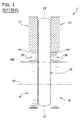
従来技術における両面研削盤の典型的なウエハクランプデバイス1’を図1および図2に概略的に示される。研削砥石9’および静水圧パッド11’は、互いに独立してウエハWを保持する。それらは、クランプ平面71’および73’を個々に規定する。ウエハWに対する研削砥石9’のクランプ圧力は砥石の回転軸67’に集中し(または中心があり:centered)、ウエハに対する静水圧パッド11’のクランプ圧力はウエハの中心WCの近くに集中する(または中心がある)。研削中にクランプ平面71’および73’が同時に保持されている限り(図1)、ウエハは平らに維持され(すなわち、曲がらず)、砥石9’によって均一に研削される。クランプ平面のアラインメントに関する一般的な議論は、米国特許第6,652,358号に見出すことができる。しかしながら、2つの平面71’および73’が正しく整列されなくなると、研削砥石9’のクランプ圧力と静水圧パッド11’のクランプ圧力とにより、ウエハW内に曲げモーメント、または静水圧クランプモーメントが生じて、研削砥石用開口(grinding wheel opening)39’の周縁部41’にほぼ隣接してウエハを鋭く曲げる(図2)。これは、ウエハW内において、高度に局在した応力の領域を形成する。
Shown schematically in Figure 1 and Figure 2 a typical weather Haq lamp device 1 'of the double-sided grinding machine in the prior art. The grinding
クランプ平面71’および73’の不整列(ミスアラインメント)は、両面研削の操作中によく起こることであり、静水圧パッド11’に対する研削砥石9’の相対的な動きによって大抵は引き起こされる(図2)。不整列が起こり得るモードを図2および3に概略的に示す。これらは、3つの異なるモードの組み合わせを含む。第1モードでは、研削砥石の回転軸67’に沿った移動において、静水圧パッド11’に対する研削砥石9’の相対的な横方向シフトSがある(図2)。第2モードは、個々の研削砥石の中心を通過する水平軸Xのまわりにおける砥石9’の垂直傾斜(vertical tilt)VTによって特徴付けられる(図2および3)。図2は、第1モードと第2モードの組み合わせを示す。第3モードでは、個々の研削砥石の中心を通過する垂直軸Yのまわりにおける砥石9’の水平傾斜(horizontal tilt)HTがある。これらのモードは、概念を説明するために図中でかなり誇張されている。実際の不整列は、比較的小さいだろう。さらに、例えば左側の砥石の水平傾斜HTが右側の砥石の水平傾斜と異なってもよいなど、各々の砥石9’は、他方とは独立して動くことができ、また2つの砥石の垂直傾斜VTについても同様である。
Misalignment of the clamp plane 71 'and 73' (misalignment) is to occur often in the double-side grinding operation, usually caused by-out relative movement of the '
クランプ平面71’および73’の不整列によって生じる静水圧クランプモーメントの大きさは、静水圧パッド11’のデザインに関連する。例えば、ウエハWのより大きい面積をクランプするパッド11’(例えば、広い加工表面積を有するパッド)、パッドクランプの中心が研削砥石の回転軸67’から比較的大きく離れて配置されているパッド、ウエハに高い静水圧パッドクランプ力を及ぼす(すなわち、ウエハを非常に強固に保持する)パッド、またはこれらの特徴の組み合わせを示すパッドによって、一般的に、より高いモーメントが生じる。
The magnitude of the hydrostatic clamping moment caused by the misalignment of the clamping planes 71 'and 73' is related to the design of the hydrostatic pad 11 '. For example,
従来技術のパッド11’(従来技術のパッドの一例を図4に示す)を用いたクランプデバイス1’では、クランプ平面71’および73’が不整列になったときのウエハW内の曲げモーメントは比較的大きい。これは、ウエハが、研削砥石用開口39’の周縁部(near peripheral edge)41’の近傍を含め、パッド11’によって非常にきつく、強固にクランプされるためである。ウエハで研削砥石9’の動作を調整することはできず、ウエハは、開口縁部41’の近傍で鋭く曲がる(図2)。ウエハWは均一に研削されず、そして次のプロセス(例えば、研磨)において除去不可能な、望ましくないナノトポロジー特徴を生じる。クランプ平面71’および73’の不整列は、研削砥石9’の不均一な磨耗を引き起こすおそれもあり、それはさらに、研削されたウエハWに望ましくないナノトポロジー特徴を生じる一因となり得る。
In the
図5Aおよび5Bは、クランプ平面71’および73’が整列しておらず、研削操作中にウエハが曲がっている場合に、研削されたウエハWの表面上に形成され得る望ましくないナノトポロジー特徴を示す。特徴は、中心マーク(C−マーク)77’およびB−リング79’を含む(図5A)。中心マーク(C−マーク)77’は、一般に、研削砥石9’の横方向シフトSと垂直傾斜VTとの組み合わせによって生じ、B−リング79’は、一般に、砥石の横方向シフトSと水平傾斜HTとの組み合わせによって生じる。図5Bに示されるように、両方の特徴77’および79’は、それらに付随する比較的大きいピークバレー変化を有する。従って、それらは、劣ったウエハナノトポロジーを示しており、ウエハ表面上に小型回路をプリントする能力に大きな影響を及ぼし得る。
5A and 5B, the clamp plane 71 'and 73' GaSei not in columns, when wafer song Ru Ttei during grinding operation, unwanted may be formed on the surface of the ground wafers W nano The topology characteristics are shown. Features include a center mark (C-mark) 77 ′ and a B-
このセクションは、本発明の様々な態様に関連し得る技術の様々な態様を読み手に紹介することを意図しており、それらは以下に記載されおよび/または特許請求される。この議論は、読み手に背景情報を提供するのに有益で、本発明の様々な態様のより良い理解を促進すると考えられる。従って、これらの記述は、この観点から読まれるべきであり、従来技術の承認(admission)として読まれるべきではないと理解すべきである。 This section, the various aspects of the function may be continuous technique to various aspects of the present invention is intended to introduce the reader, they are claimed and / or patent described below. This discussion is useful for providing background information to the reader and is believed to facilitate a better understanding of the various aspects of the present invention . Therefore, these descriptions are to be read in this light, it should be understood not to be read as an admission slave come Technology (admission).
1つの態様は、一対の研削砥石と、その中に静水圧を有する一対の静水圧パッドとの間にウエハを保持するタイプの両面研削盤を用いて半導体ウエハを処理する方法である。研削盤は、研削盤によって引き込まれた電流を検出するためのパターン検出ソフトウェアを含むプロセッサを含む。この方法は、ウエハをクランプする段階と、ウエハを研削する段階と、ウエハを研削砥石との接触から離す段階とを含む。この方法は、さらに、各々の段階を検出するためのソフトウェアを使用すること、各々の段階における静水圧を変えて、ウエハに適用されるクランプ圧力を変え、それにより処理したウエハのナノトポロジーを改善することを含む。 One embodiment, Ru method der of processing a semiconductor wafer using a pair of grinding wheels, the type of double-sided grinding machine for holding the wafer between a pair of hydrostatic pad having a hydrostatic pressure in it. Grinder includes a processor including a pattern detection software for detecting current drawn by the grinding machine. The method includes the steps of clamping a wafer, a step of grinding the wafer, the wafer and the contact or et away to the stage of the grinding wheel. The method further includes the use of software for detecting each step, changing the hydrostatic pressure in each of the stages, changing the clamping pressure applied to the wafer, improve it by nanotopology of the wafer treated Including doing .
別の態様は、研削操作中に一対の研削砥石と一対の静水圧パッドとの間にウエハを保持するタイプの両面研削盤を用いて半導体ウエハを処理する方法である。この方法は、研削操作の第1段階において、静水圧パッド内に第1静水圧を確立してウエハを最初にクランプすることを含む。研削操作の第2段階でウエハを研削する間に、第1圧力よりも低い第2静水圧まで静水圧を減少させる。研削操作の第3段階において第3静水圧まで静水圧を増加させてウエハをクランプし、これにより処理されたウエハのナノトポロジーを改善する。 Another aspect is a method for processing a semiconductor wafer using a double-sided grinder of the type that holds the wafer between a pair of grinding wheels and a pair of hydrostatic pressure pads during a grinding operation . The method includes establishing a first hydrostatic pressure in the hydrostatic pad and first clamping the wafer in a first stage of the grinding operation. During grinding the wafer in the second stage of grinding operation, to reduce the hydrostatic pressure to a lower second hydrostatic pressure than the first pressure. In the third stage of the grinding operation, the hydrostatic pressure is increased to the third hydrostatic pressure to clamp the wafer , thereby improving the nanotopology of the processed wafer.
さらに別の態様は、一対の研削砥石と、プロセッサと、一対の静水圧パッドとを含む両面研削盤である。研削砥石と静水圧パッドとは、ほぼ平坦なウエハを、一対の研削砥石の間に配置されているウエハの第1部分と一対の静水圧パッドの間に配置されているウエハの第2部分とが同一平面内で保持されるように操作可能である。静水圧パッドは、静水圧を維持するように静水圧パッドを通過して流れる水を含む。研削盤は、パッドを通過する水の流速(または流量、flow rate)を制御するための、それにより静水圧を制御するための、流量制御弁を更に含む。流量制御弁は、プロセッサによって制御される。 Yet another aspect is a double-sided grinding machine that includes a pair of grinding wheels, a processor, and a pair of hydrostatic pressure pads. The grinding wheel and the hydrostatic pads, the substantially flat wafer, and a second portion of the wafer being disposed between the first portion and a pair of hydrostatic pads of the wafer being disposed between the pair of grinding wheels There is operable to be held in the same plane. The hydrostatic pad includes water that flows through the hydrostatic pad to maintain the hydrostatic pressure . The grinder further includes a flow control valve for controlling the flow rate of water through the pad , thereby controlling the hydrostatic pressure. The flow control valve is controlled by the processor.
上述した態様に関して記載された特徴には、様々な改良が存在する。更なる特徴は、同様に、上述した態様に組み込まれ得る。これらの改良および付加的な特徴は、個々にまたは任意の組み合わせで存在し得る。例えば、図解した実施形態のいずれかに関連して以下に議論様々な特徴は、単独で、または任意の組み合わせで、上述した態様のいずれかに組み込まれ得る。 The feature described with respect to the aspects above mentioned, there are various modifications. Additional features can be incorporated into the embodiments described above as well. These refinements and additional features may exist individually or in any combination. For example, various features discussed below in relation to any of the illustrated embodiment is a alone or in any combination, it may be incorporated into any of the embodiments described above.
対応する参照記号は、添付図面の複数の図全体を通して対応する部分を表す。 Corresponding reference characters indicate corresponding parts throughout the several views of the accompanying drawings.
図を再び参照すると、図6および7は、一般に符号1で示した本発明に係るウエハクランプデバイスを概略的に示す。 When figure Referring again to FIG. 6 and 7 show generally a wafer clamping device according to the present invention shown in sign-1 schematically.
クランプデバイスは、一般に図6の符号3で示した両面研削盤内で用いることがでる。 Clamping device, it is out of use generally a double-sided grinding machine in shown in sign-3 of Figure 6.
ウエハクランプデバイス1を用いることができる両面研削盤の例は、光洋機械工業株式会社製のモデルDXSG320およびモデルDXSG300Aを含む。
Examples of double-sided grinding machine can be used weather
ウエハクランプデバイス1は、ウエハの両表面を同時に均一に研削できるように、図中で一般にWで示される単一の半導体ウエハ(広義には「ワークピース(workpiece)」)を、研削盤3内に垂直姿勢で保持している。
Weather-
これは、研磨工程および回路プリント工程の前に、ウエハの表面の平坦度および平行度を改善する。 This is prior to the polishing process and circuit printing process, to improve the flatness and parallelism of the surface of the wafer.
研削盤は、本発明の技術的範囲から逸脱せずに、半導体ウエハ以外のワークピースを保持するクランプデバイスを有してよいことを理解されたい。 It should be understood that the grinding machine may have a clamping device that holds workpieces other than semiconductor wafers without departing from the scope of the present invention.
図6および7にも示されるように、ウエハクランプデバイス1は、一般に符号9a、9bでそれぞれ示した左右の研削砥石、および一般に符号11a、11bでそれぞれ示した左右の静水圧パッドを含む。
As also shown in Figure 6 and 7, weather
左右の指定は、ただ記載を簡易にするためになされており、および砥石9a、9bとパッド11a、11bのいかなる特定の方向をも要求しない。
The left and right designations are made merely for ease of description and do not require any specific orientation of the
文字「a」および「b」は、左側の砥石9aと左側のパッド11aとの部分を、右側の砥石9bと右側のパッド11bのものと区別するのに用いる。研削砥石9a、9bと静水圧パッド11a、11bは、当業者に既知である手段によって研削盤3に取り付けられる。
Letter "a" and "b" are used portions of the
従来から知られているように、2つの研削砥石9a、9bは、実質的に同じであり、各々の砥石は、ほぼ平坦である。
As is known in the art, the two
図6および7に示すように、研削砥石9a、9bは、一般に、ウエハの中心から下側で(または下側中心に向かって:toward a lower center of the wafer)、ウエハWとの係合部を研削するために置かれている。
As shown in FIGS. 6 and 7, the grinding
各々の砥石9a、9bの外縁は、ウエハの下端におけるウエハWの外縁より下まで延在し、ウエハの中心におけるウエハの中心軸WCより上まで延在している。
Each
これは、各々のウエハWの表面積全体を操作中に研削することを確実にする。 This ensures that the entire surface area of each wafer W is ground during operation.
加えて、研削砥石9a、9bの少なくとも一方は、その対にされた研削砥石に対して相対的に移動可能である。
In addition, at least one of the grinding
これは、研削盤3のクランプデバイス1内の研削砥石9a、9bの間の位置に半導体ウエハWを装填する(または入れる:load)のを容易にする。
This facilitates loading of the semiconductor wafer W at a position between the grinding
図示されたクランプデバイス1においても、半導体ウエハWをデバイス1内に装填するのが更に容易になるように、左側の静水圧パッド11aは、対応する左側の研削砥石9aに対して相対的に移動可能であり、また、固定されたままの右側の静水圧パッド11bに対しても移動可能である。
Also in the
両方のパッドが対応する研削砥石に対して相対的に移動可能なウエハクランプデバイス、ウエハを装填中に両方のパッドを固定するウエハクランプデバイス、またはウエハを装填中に静水圧パッドと対応する研削砥石とが共に動くウエハクランプデバイスは、本発明の技術的範囲から逸脱しない。 Both pads corresponds to the grinding wheel against the relatively movable weather Haq lamp device, a hydrostatic pad weather Haq lamp device to fix both pad during loading the U Fine, or wafer during loading corresponding grinding wheel are both moved weather Haq lamp device, without departing from the scope of the present invention.
図6および7に示したウエハクランプデバイス1をまた参照すると、研削操作中に、ウエハクランプデバイスの2つの研削砥石9a、9bと、2つの静水圧パッド11a、11bは、それらの間に半導体ウエハWを保持するために、向かい合った関係で配置されている。
Also referring to weather
研削砥石9a、9bおよび静水圧パッド11a、11bは、垂直なクランプ平面71、73をそれぞれ規定し、ウエハを垂直姿勢で保持するのを支援するクランプ圧力を、ウエハW上に生み出す。
The grinding
このことは、以下に更に詳細に説明する。 This is you described in further detail below.
図6をとりわけ参照すると、静水圧パッド11a、11bは、操作中に静止しているが、一般に符号14で示されるドライブリングはウエハを動かして、パッドおよび研削砥石9a、9bに対して相対的に回転させる。
With particularly referring to FIG. 6, the
従来から知られているように、ドライブリング14の戻り止め(detent)またはクーポン(coupon)15は、一般に、ウエハの外縁に形成された切欠きN(図6では破線で示される)においてウエハWと係合して、ウエハを動かし、その中心軸WC(中心軸WCは、パッド11a、11bの水平軸44a、44bにほぼ対応する(図8および図12を参照))のまわりに回転させる。
As is known in the art, detent (detent) or coupon (coupon) 15 of the
同時に、研削砥石9a、9bは、ウエハWと係合し、互いに反対の方向に回転する。
At the same time, grinding
砥石9a、9bの一方は、ウエハWと同じ方向に回転し、他方は、ウエハとは反対の方向に回転する。
次に図8〜13Bを参照すると、本発明の静水圧パッド11a、11bは、更に詳細に示されている。
Referring now to FIG. 8~13B,
図8〜11は、左側の静水圧パッド11aを示し、図12〜13Bは、向かい合った右側の静水圧パッド11bを示す。
8-11 shows the
図示されるように、2つのパッド11a、11bは実質的に同じであり、互いにほぼ鏡像である。
As shown, two
従って、左側のパッド11aだけが説明され、右側のパッド11bの説明は同じであると理解されるだろう。
Therefore, only the left-
図8〜9Bに示すように、左側の静水圧パッド11aは、概して薄く、円形形状であり、処理されるウエハWと同様の寸法を有する。
As shown in FIG. 8~9B, left side of the
この関係を示すために、図9Aおよび9Bに、ウエハWを鎖線で図示した。 In order to show this relationship, the wafer W is illustrated by a chain line in FIGS . 9A and 9B .
図示された静水圧パッド11aは、直径が約36.5cm(14.4in)で、操作中にウエハWと向かい合う加工表面積が約900cm2(139.5in2)である。の
The illustrated
従って、例えば、直径が約300mmの標準的なウエハを研削するのに用いることができる。 Thus, for example, it can be used to grind the standard specific wafer about 300mm in diameter.
とはいえ、静水圧パッドは、本発明の技術的範囲から逸脱せずに、異なる直径および表面積にしてもよいことを理解すべきである。 Nonetheless, it should be understood that the hydrostatic pressure pads may be of different diameters and surface areas without departing from the scope of the present invention.
例えば、パッドは、200mmのウエハの研削に用いるための小さいスケールの寸法にしてもよい。 For example, the pad may be a small-scale dimensions for use in grinding of 200mm wafers.
図8および9Aから最もよくわかるように、静水圧パッド11aの本体17aは、研削操作中にウエハWに直接向かい合った(immediately opposite)ウエハ側の面19aを含む。
As best seen in FIGS. 8 and 9A, the
ウエハ側の面19aに形成されている6つの静水圧ポケット21a、23a、25a、27a、29a、31aは、それぞれ、パッド11aの研削砥石用開口(一般に符号39で示される)のまわりにほぼ半径方向に配置されている。
パッド本体17aの後面35aは、ウエハ側の面19aの反対側にあり、ほぼ平坦で静水圧ポケットは無いが、本発明の技術的範囲から逸脱せずにポケットを含んでよい。
加えて、6つより多いまたは少ない静水圧ポケット、例えば、4つのポケットを有する静水圧パッドは、本発明の技術的範囲から逸脱しない。 In addition, hydrostatic pressure pads having more or less than six hydrostatic pockets, eg, four pockets, do not depart from the scope of the present invention.
6つの静水圧ポケット21a、23a、25a、27a、29a、31aは、それぞれ、アーチ形状であり、パッド11aのまわりにほぼ周方向に延在している。
Six
それぞれのポケット21a、23a、25a、27a、29a、31aは、ウエハ側の面19aにおける盛り上がった表面(raised surface)32a内で凹んでおり、それぞれが、比較的平坦な垂直側壁(flat vertical sidewalls)37aと、丸みを帯びた外周角部(rounded perimeter corners)とを含む。
Each
ポケットは、パッド11aの面19aに、浅いキャビティを切削または成型(casting)することによって形成されている。
The pocket is formed by cutting or casting a shallow cavity on the
異なるプロセスで形成した静水圧ポケットは、本発明の技術的範囲から逸脱しない。 Hydrostatic pressure pockets formed in different processes, without departing from the scope of the present invention.
図8および9Aを再度参照すると、ポケット21aと23a、25aと27a、および29aと31aの対の各々は、実質的に同じ寸法および形状にされることがわかる。
8 and 9A again, each pair of
更に、図示されたパッド11aでは、ポケット21aおよび23aの各々は、表面積が約14.38cm2(2.23in2)で、ポケット25aおよび27aの各々は、表面積が約27.22cm2(4.22in2)である。およびポケット29aおよび31aは、それぞれ、約36.18cm2(5.61in2)の表面積を有する。
Further, in the illustrated
パッドの全ポケット表面積11aは、約155.56cm2(24.11in2)であり、全ポケット表面積のパッド加工表面積に対する割合は、約0.17である。
The total
この割合は、0.17以外であってもよく、それでも、本発明の技術的範囲内にある。例えば、割合は、約0.26以下であってよい。従来のパッド11’(図4)と比較すると、ポケット21’、23’の各々の表面積は、約31.82cm2(4.93in2)であり、ポケット25’、27’の各々の表面積は、約36.47cm2(5.65in2)であり、ポケット29’、31’の各々の表面積は、約47.89cm2(7.42in2)である。従来のパッド11’の全ポケット表面積は、約232.36cm2(36.02in2)であり、全ポケット表面積に対するパッド加工表面積の割合は、約0.26(パッド11’の加工表面積は、約900cm2(139.5in2 ))である。
This ratio may be other than 0.17 and is still within the scope of the present invention. For example, the ratio may be about 0.26 or less. 'Compared to (4), the pocket 21'
ポケット21aと23a、25aと27a、および29aと31aは、それぞれ、(パッド11aの垂直軸43aで分割された)ウエハ側の面19aの左右半分づつ(または、反対側の半分:opposite halves)に、対称的に配置されている。ポケット21a、23aは、一般に、パッド11aの水平軸44aよりも下側にあるが、ポケット25a、27a、29a、31aは、一般に、軸44aよりも上側にある。ポケット29a、31aは、一般に、ポケット25a、27aより上側にあり、研削砥石用開口39aに隣接して配置されておらず、それの間に配置されたポケット25a、27aにより開口から分離されている。このポケットの配向において、全ポケット表面積の約15%が、水平軸44aより下側に位置する。このパーセントは、本発明の技術的範囲から逸脱せずに23%以下であり得る。従来のパッド11’と比較すると、全ポケット表面積の少なくとも約24%が、パッドの水平軸44’より下側に位置する。軸44’より下側のポケット面積が増加することによって、パッド11’によりウエハにかけられるクランプ力は、研削砥石用開口39’側に向かって増加し、B−リング形成の一因となることを理解すべきである。
図8および9Aは、静水圧パッド11aの本体17aの下側部分に形成された円形の研削砥石用開口39aを示しており、パッドを貫通しウエハWの中心から下側と係合する研削砥石9aを、収容できる寸法および形状にされている(研削砥石およびウエハは、図9Aにおいて鎖線で示される)。開口に収容したときに、開口39aの中心は研削砥石9a(および9b)の回転軸67にほぼ対応する。図示されたパッド11aでは、研削砥石用開口39aの半径R1は約87mm(3.43in)であり、研削砥石9aの周縁部と、半径方向に向かい合う研削砥石用開口縁部41aとの間の距離は、比較的均一であり、おおむね約5mm(0.20in)である。これらの距離は、本発明の技術的範囲から逸脱せずに異なってよい。
8 and 9A show a circular
図示するように、パッド11aの盛り上がった表面32aは、各々のポケット21a、23a、25a、27a、29a、31aの外周を囲むように延在している同一の広がりを有する平坦域((または、同一の広がりを有する高台部分:coextensive plateaus)34aを含む。符号36aでそれぞれ示した排水チャンネルは、ポケット21a、23a、25a、27a、29a、31aの各々の平坦域34aの間において、盛り上がった表面32aに形成されている。おおよそ三日月形の自由領域60aは、研削砥石用開口の周縁部41aと、ポケット21a、23a、25a、27aの平坦域34aの内側部分の縁部38aとの間において、盛り上がった表面上で凹んでいる。
ウエハWに対するクランプ力は、自由領域60aでは実際上ゼロである。これらの特徴を以下に更に説明する。
As shown in the drawing, the raised
The clamping force on the wafer W is practically zero in the
図10を参照すると、静水圧ポケット21a、23a、25a、27a、29a、31aは、それぞれ、流体をポケットに導入するための流体注入ポート61aを含む。パッド本体17a内のチャンネル63a(隠れ線によって示される)は、流体注入ポート61aと相互接続されており、流体を、外部流体源(図示せず)からポケットに供給する。研削中に、パッド面19aではなく流体がウエハWと接触するように、操作中に、比較的一定の圧力下で、流体をポケット21a、23a、25a、27a、29a、31aに送り込む。このように、ポケット21a、23a、25a、27a、29a、31aでの流体は、ウエハWをパッドクランプ平面73内で垂直に保持する一方で(図6および7を参照されたい)、ウエハWが研削中に非常に低い摩擦抵抗でパッド11a(および11b)に対して相対的に回転可能になる、潤滑されたベアリング領域またはスライドバリア(sliding barrier)を提供する。パッド11aのクランプ力は、主に、ポケット21a、23a、25a、27a、29a、31aに提供される。
Referring to FIG. 10, the
図11は、パッド11aのウエハ側の面19aの左半分を更に詳細に参照し、ポケット21a、25a、29aの配向を示す。半径距離(または半径方向の距離)RD1、RD2およびRD3は、理想的には研削砥石の回転軸67に対応する研削砥石用開口の中心からの、ポケット21a、25aおよび29aのそれぞれについて最も近い垂直側壁37a(最も近い垂直側壁37aは、研削砥石用開口39aの縁部41aに最も近い垂直側壁のことである)の周縁部の位置を示す。図示するように、距離RD1は、ポケット21aの最も近い垂直側壁37aのまわりにおいて一定ではなく、ポケット21aの下端(bottom end)からのほうが、上端からよりも開口39aまで遠い。具体的には、距離RD1は、ポケットの下端の方向で約104mm(4.1in)から、上端の方向で約112mm(4.4in)の範囲である(これらの値は、ポケット23aと同じである)。半径距離RD2およびRD3は、それぞれ、ポケット25aおよび29aの最も近い垂直壁37aまで比較的一定であり、RD2が約113mm(4.4in)の値であり、RD3が約165mm(6.5in)の値である(これらの値は、ポケット27a、31aのそれぞれと同じである)。本発明の技術的範囲から逸脱せずに、半径距離RD1は一定であってよく、半径距離RD2およびRD3は一定でなくてよい。
Figure 11 is a further particular reference to the left half of the
図11は、また、研削砥石の回転軸67から、ポケット21a、25aの平坦域34aの半径方向に最も内側の縁部38aまで半径方向に測定した半径距離RD11を示す。縁部38aは、ゼロ圧力の(自由な:free)領域60aの末端または境界を規定する。図から分かるように、半径距離RD11は縁部38aに対して一定ではなく、図示されたパッド11aでは、垂直軸43の近傍における約108mm(4.25in)から、縁部38aが研削砥石の開口縁部41aと合体する位置であるポケット21aの下端近傍における約87mm(3.43in)までの範囲にある。研削砥石9aの周縁部(開口39aに収容したとき)から、半径方向に向かい合った縁部38aの最深部分(a radially opposed innermost portion)までを、これらと同じように測定すると、垂直軸43aの近傍における約26mm(1.02in)から、ポケット21aの下端近傍における約5mm(0.20in)までの範囲にあり、研削砥石用開口39aの半径R1に対する割合は、約0.30〜約0.057の範囲となる。比較すると、従来の静水圧パッド11’(図4)における対応する距離は一定であり、これは、盛り上がった表面32’の最深部分の周縁部38’は、研削砥石の開口縁部41’と一致する(すなわち、従来のパッド11’内にゼロ圧力の(自由な)領域がない)からである。このパッド11’では、半径距離RD11’は、約87mm(3.43in)であり、研削砥石9’の周縁部から縁部38’までの同じ測定は、約5mm(0.20in)である。
FIG. 11 also shows the radial distance RD11 measured in the radial direction from the rotating
本発明の静水圧パッド11aおよび11bは、従来の静水圧パッド11’と比較して少なくとも以下の好都合な特徴を有する。全静水圧ポケット表面積は減少する。これは、パッドによってウエハWに適用される全体のクランプ力を効果的に減少し、これは、操作中に静水圧ポケット21a、23a、25a、27a、29a、31a、21b、23b、25b、27b、29b、31bに収容される流体の量が減少するからである。加えて、水平軸44aより下側にあるポケット表面積は減少する。これは、研削砥石用開口39a、39bの左側および右側におけるクランプ力をとりわけ低くする。更に、内側ポケット21a、23a、25a、27a、21b、23b、25b、27bは、研削砥石用開口縁部41a、41bから離れ、それらの間にゼロ圧力の自由領域60a、60bが形成される。これは、研削砥石用開口39a、39bの縁部41a、41bのまわりのクランプ力をとりわけ低くする。
The
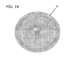
研削砥石9a、9bのシフト動作および/または傾斜動作を更に容易に一致させることができるように、ウエハWを研削操作に静水圧パッド11a、11bであまり強固ではなく保持する。これは、研削砥石9a、9bが移動するときに形成される静水圧クランプモーメントの大きさを減少する(すなわち、ウエハの曲げ領域に形成される応力が小さくなる)。加えて、ウエハWを、研削砥石用開口縁部41aに隣接して、きつく保持しない。砥石が移動するときに、ウエハWは、研削砥石用開口縁部41aに隣接して曲がる可能性はやはりあるが、従来の研削デバイスよりは鋭くはない。従って、静水圧パッド11aおよび11bは、ウエハWの表面に亘る更に均一な研削を促進し、研削したウエハのB−リングおよび中心−マーク(C−マーク)の形成などのナノトポロジー悪化を減少または排除する。これは、図5Aと14を比較することによってわかる。図5Aは、従来の静水圧パッド11’を用いて研削されたウエハWを示し、図14は、本発明のパッド11aおよび11bを用いて研削されたウエハWを示す。図14に示されるウエハは、B−リングおよび中心−マーク(C−マーク)が実質的に存在しない。
Grinding
図15A〜19は、本発明のパッド11a、11bおよび従来のパッド11’で保持したウエハW内の応力を示す。図15Aおよび15Bは、研削砥石および静水圧パッドのクランプ平面が整列(または調整:align)したときの、これらの応力を視覚的に図示する。両方のウエハWにおいて、研削砥石用開口39および39’内の応力は無視してよい(パッドは、これらの領域ではウエハをクランプしない)。図15Aは、パッド11aおよび11bによって保持されたときにウエハWに形成される低い応力を示す。それは、特に、研削砥石用開口縁部41a、41bに隣接したウエハWの全体表面に亘って低い応力(98および99で示した明るい色の領域)を示す。それはまた、ウエハに亘る均一に分布された応力も示す。一方で、図15Bに示されるように、パッド11’によって保持されたウエハW内の最大の応力97は、開口39’の周縁部に近接している(すなわち、ゼロ圧力(自由)領域がない)。
FIG 15A~19 shows stresses in the wafer W held by
図15Aおよび15Bを比較してわかるように、大きな応力が集中する領域97は、パッド11aおよび11bを用いての研削中には、パッド11’(図15B)を用いたときほどには広がらない。利点は、(例えば、研削砥石用開口縁部41aに隣接した)曲げ領域におけるウエハWの局所的な変形が少ないことと、研削砥石9a、9bのより均一な磨耗と、の両方である。砥石の均一な磨耗は、砥石の形状が、研削中に変化しない(すなわち、差別的な(または特異的な:differential)研削磨耗がない)ことを確実にする。これは、研削盤が、長期間に亘って、低いナノトポロジーの設定を維持できることも保証する。また、砥石がシフトまたは傾斜したときに、動作によって生じる応力をウエハWに亘って効果的に広げて、中心−マーク(C−マーク)およびB−リングをあまり目立って形成させない。これにより、望ましくは、研削のナノトポロジーが、研削砥石のシフトおよび傾斜による影響を受けにくくなる。
As can be seen by comparing FIGS. 15A and 15B, a region 97 in which large stress is concentrated, during grinding using the
図16〜19は、研削砥石9a、9bがシフトおよび/または傾斜したときに、静水圧パッド11a、11bを用いた研削操作中のウエハW内の応力が低いことを示している。図示された応力は、研削砥石用開口縁部41a、41bに隣接したウエハW内に生じるものであり、縁部41a、41bのまわりの位置において、約7時の位置(弧の長さ(arc length)0mm)から始めて、周縁部を時計回りに移動して(弧の長さ約400mmまで)測定される。従来の静水圧パッド11’で保持されるウエハW内の応力は、一般に符号91で示し、パッド11a、11bで保持されるウエハ内の応力は、一般に符号93で示す。
Figure 16-19, grinding
図16は、研削砥石がシフトしたときの応力91、93を示す。図から分かるように、応力93は、応力91より顕著に小さく、ウエハWの中心WC(約200mmの弧の長さに対応する)を含む研削砥石用開口39a、39bの外縁全体にわたって、応力91に比べて更にほとんど一定である。従って、本発明において、研削砥石9a、9bがシフトしたときに、ウエハWは、従来のデバイスで研削されるウエハと比較して、それらの中心の近傍で鋭く曲がらない。
FIG. 16 shows the
図17は、研削砥石がシフトして垂直傾斜したときの、ウエハW内の応力91、93を示す。再び、パッド11a、11bに関連する応力93は、研削砥石用開口縁部39a、39bの外縁全体に沿ってほぼ一定である。加えて、ウエハ中心WCに対応する位置でパッド11a、11bによって保持されたウエハW内の応力93の増加は著しく少ない。従って、研削砥石9a、9bがシフトして垂直傾斜したときに、ウエハWは、研削砥石用開口39a、39bの外縁に隣接してそれほど鋭く曲がらず、中心−マーク(C−マーク)の形成は減少する。
FIG. 17 shows the
図18は、砥石がシフトして水平傾斜したときのウエハW内の応力91、93を示す。図から分かるように、ウエハWの左側における応力93は、応力91のようには鋭く増加しない。従って、パッド11a、11bで保持されたウエハWは、砥石9a、9bがシフトして水平傾斜したときにそれらの外縁ではそれほど鋭く曲がらず、B−リングおよび/またはC−マークの形成は減少する。研削砥石のシフトと垂直傾斜と水平傾斜との組み合わせ効果によってウエハW内の応力91、93が生じる場合の同様の結果を図19に示す。
FIG. 18 shows stresses 91 and 93 in the wafer W when the grindstone is shifted and tilted horizontally . As can be seen, the
図20は、従来の静水圧パッド11’および本発明の静水圧パッド11a、11bを用いて研削されたウエハについて、上位0.05パーセンタイルのナノトポロジー値を図に記したものである。パッド11’を用いて研削されたウエハのナノトポロジー値は、一般に符号72で示されており、パッド11a、11bを用いて研削されたウエハの値は、一般に符号74で示される。本発明のパッド11a、11bを用いて研削されたウエハは、一貫して従来の値72より低いナノトポロジー値74を有する。
Figure 20 is a
本発明の静水圧パッド11a、11bは、単一の操作セットアップ(operational set-up)で、ウエハのセット(または一連のセット:a set of wafers)における多数のウエハを研削するのに用いることができる。ウエハのセットは、例えば、少なくとも400枚のウエハを含み得る。それは、本発明の技術的範囲から逸脱せずに、400枚よりも多いウエハを含んでよい。単一の操作セットアップは、研削砥石9a、9bの手動調整の間に、一般に考慮される連続的な操作である。研削されたウエハWのセットの各々は、一般に、改善されたナノトポロジーを有する(例えば、中心マーク(C−マーク)およびB−リングの形成が、減少または排除されている)。とりわけ、それらの各々は、平均ピークバレー変化が約12mm未満である。例えば、ウエハの平均ピークバレー変化は、約8nmであってよい。平均ピークバレー変化は、各々のウエハWの平均半径スキャン(an average radial scan)における変化を表す。ピークバレー変化は、ウエハWの外縁の辺りで、多数のウエハ半径において求められ、それらの値の平均は、平均的な変化を定める。
The
図21は、本発明の第2の実施形態に従って左側の静水圧パッドを概略的に示す。パッドは、一般に符号111aで示し、第1の実施形態のパッド11aの部分に対応するこのパッドの部分は、同じ符号に「100」を足して示す。この静水圧パッド111aは、これまで記載した静水圧パッド11aと実質的に同じであるが、パッド11aの対応するポケット21a、23a、25a、27a、29a、31aとは異なる形状および方向にされている静水圧ポケット121a、123a、125a、127a、129a、131aを有する。パッド11aと同様に、ポケット121a、123a、125a、127a、129a、131aは、パッド111aの研削砥石用開口139aのまわりに半径方向に配置されており、ポケット121aと123a、ポケット125aと127a、ポケット129aと131aは類似しており、ウエハ側の面119aの左右半分づつ(または、反対側の半分)に、おいて対称的に配置されている。加えて、ポケット121a、123aは、パッド111aのまわりに周方向に延在している。しかしながら、このパッド111aでは、ポケット125a、127a、129a、131aは、研削砥石用開口139aからに離れて半径方向に延在している。その他の全ての態様については、これらのパッド111a、111bは、パッド11a、11bと同じである。
Figure 21 illustrates schematically a hydrostatic pad on the left side in accordance with a second embodiment of the present invention. Pad, generally indicated by the sign-111a, the portion of the pad corresponding to the portion of the
静水圧パッドのクランプの中心が、静水圧パッドのポケットにかかる水圧を制御することにより影響を受け得ることが、追加的に考慮される。これは、クランプの中心を下げ、ウエハクランプデバイスの研削砥石の回転軸の近くに動かすだろう。更にとりわけ、各々のポケット(またはポケットのいくつかのサブセット)内での流体圧力は、一連の研削(the course of grinding)の間に変化させ得、および/または他のポケットから独立して制御され得る。いくつかのポケットの間で圧力を変える1つの方法は、ポケット内のオリフィス開口の寸法を異ならせることである。
更に、各々のポケットに関連する領域の剛性(stiffness)は、ポケット深さを異ならせることによって、ポケットの間で変えることができる。深いポケットは、深いポケットの領域において、浅いポケットに比べてウエハWの柔軟な(compliant)保持をもたらし、浅いポケットの領域においてウエハを強固に保持する。
Center of the clamp of the hydrostatic pads, the be affected by controlling the pressure applied to the pockets of the hydrostatic pads, Ru is considered additionally. This lowers the center of the clamp would be near Ku the dynamic dregs of the rotation axis of the grinding wheel of the upper Haq lamp device. More particularly, the fluid pressure within the respective pockets (or some subset of the pocket) are independently controlled to obtain varying between a series of grinding (the course of grinding), and / or from another pocket Can be done. One method may varying the pressure between the several pockets is to vary the size of the orifice opening in the pocket.
Furthermore, the rigidity of the regions associated with each pocket (Stiffness), by varying the pocket depth can be changed in between the pocket. Deep pockets, in the area of the deep pocket, compared to the shallow pocket and cod also a flexible (compliant) retention of the wafer W, to firmly hold the wafer have you in the area of the shallow pocket.
本明細書で図示され記載された静水圧パッド11a、11b、111a、111bは、約300mmの直径を有するウエハWとともに用いるために記載される。これまでに示されるように、静水圧パッドは、本発明の技術範囲から逸脱せずに、200mmのウエハを研削するのに用いるための縮小したスケールの寸法にできる。これは、本明細書に記載された各々の静水圧パッド寸法に適用する。
本発明の静水圧パッド11a、11bは、研削操作の間にウエハWを支持でき、そして繰り返しの研削の使用に耐えることができる好適な硬質材料、例えば金属から作られている。他の同様な硬質材料から作られている静水圧パッドは、本発明の技術的範囲から逸脱しない。
本発明の別の態様によれば、ウエハが両面研削盤内にある間に、ナノトポロジーを評価するためのシステムは、ウエハナノトポロジーにフィードバックを提供し始め。ナノトポロジー評価システムは、ワークピースが両面研削盤内に保持されている間にワークピースの位置および/または変形についての情報を収集するために配置された少なくとも1つのセンサを含む。センサは、ウエハの有限要素構造分析に用いられる1以上の境界条件を規定するのに用いる1以上の測定を行うために使用可能である。システムは、本発明の技術的範囲から逸脱せずに、(センサを用いずに規定または仮定できる境界条件を含め、有限要素分析を行うのに充分な境界条件が存在する限りは、)単一の境界条件の規定に用いられる単一の測定を行う単一のセンサのみを有してよいことを理解されたい。しかしながら、いくつかの実施形態において、ウエハの有限要素構造分析のための付加的な境界条件を規定するように、1以上のセンサは、多数の境界条件を規定するのに用いる複数の測定を行い、それはしばしば望ましい(または必要である)と認識される。 According to another aspect of the present invention, while the wafer is in the double-sided grinding machine in a system for evaluating the nanotopology begins to provide feedback to the wafer nanotopology. Nanotopology evaluation system includes at least one sensor disposed to collect information about the position and / or deformation of the workpiece while the workpiece is held on both sides grinder within. Sensors can be used to perform one or more measurements used to define one or more boundary conditions used finite elements wafer structure analysis. The system is single (as long as there are sufficient boundary conditions to perform finite element analysis, including boundary conditions that can be defined or assumed without the use of sensors) without departing from the scope of the present invention. it is to be understood that may have only a single sensor for the single measurement that used the provisions of the boundary conditions. However, in some embodiments, one or more sensors perform multiple measurements used to define multiple boundary conditions so as to define additional boundary conditions for finite element structural analysis of the wafer. , It is often recognized as desirable (or necessary).
例えば、一般に301で示した本発明のナノトポロジー評価システムの1つの実施形態は、図22、23に概略的に示す。この実施形態は、特定の静水圧パッド配置を有する両面研削盤と組み合わせて記載されるけれども(以下に記載される図25A、25Bにおいて明らかであるように)、ナノトポロジー評価システムは、本発明の技術的範囲から逸脱せずに、(別のワークピースクランプシステムを有する)他の両面研削盤とともに用いるのに適していることを理解されたい。更に、本発明は、ナノトポロジーシステム自体に限定されず、本発明のナノトポロジー評価システムを備えた両面研削装置も含む。 For example, one embodiment of the nanotopology evaluation system of the present invention shown generally at 301, schematically shown to 22 and 23. Although this embodiment is described in combination with a double-sided grinder with a specific hydrostatic pad arrangement (as will be apparent in FIGS. 25A and 25B described below), the nanotopology evaluation system is not without departing from the scope, it is to be understood that it is suitable for use with (having another workpiece clamping system) other double-sided grinding machine. Furthermore, the present invention is not limited to the nanotopology system itself, but also includes a double-side grinding apparatus provided with the nanotopology evaluation system of the present invention.
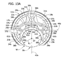
1以上のセンサ303(例えば、複数のセンサ)は、静水圧パッド305の内側表面に配置されている。図に示される特定の実施形態において、例えば、複数のセンサ303(例えば、4つ)は、静水圧パッド305の各々の内側加工表面に沿って配置されている(図23)。ウエハの有限要素構造分析のための境界条件を規定するのに使用できる情報を収集できる任意の種類のセンサを使用できる。例えば、1つの実施形態において、センサ303は、ウエハに対して制限するノズルから出る加圧された空気の流れによって受けた抵抗を測定することによって、静水圧パッドとウエハWとの間の距離を測定する動的な空気圧力センサを含む(例えば、MARPOSS Model E4Nによって製造される)。加圧された空気を大気に排出する。このようなノズルは、静水圧パッド305に強固に取り付けることができ、または別の方法では、静水圧パッドに対して固定することができる。当業者が認識するように、このような動的な圧力センサ303からの測定は、静水圧パッド305と、ウエハWの表面との間の空間を示す。従って、動的な空気圧力センサによる圧力の測定は、センサ303と、ウエハWの表面との間の距離に対応する。
One or more sensors 303 (eg, a plurality of sensors) are disposed on the inner surface of the
各々の静水圧パッド305に関連するナノトポロジー評価システムのセンサ303は、ウエハWをx、y平面で保持するように規定したx、y、z直交座標系(図22および23)のx方向とy方向の少なくとも1つにおいて、その静水圧パッドに関連する他のセンサから空間をあけられている。このように、(複数の)センサ303を離すことにより、1つのセンサを、ウエハWの表面上の対応する1つの位置の測定を行うのに使用し、そして別のセンサを、ウエハの表面上の対応する異なる位置の測定を行うのに使用するのが容易になる。
更に、図面に示される実施形態の各々の静水圧パッド305は、同じ数のセンサ303を有し、パッドの1つにおけるセンサの分配(または分布:distribution)は、実質的に、他のパッドにおけるセンサの分配(または分布)の鏡像である。結果として、両方の静水圧パッド305は、x、y、z座標系のx方向とy方向の少なくとも1つにおいて分離されたセンサ303を有する。更に、図23に示すように、静水圧パッド305を互いに向かい合って配置する場合に(例えば、研削盤が使用中である場合に)、1つの静水圧パッドにおける各々のセンサを、他の静水圧パッドにおけるセンサと対にすることにより、センサ303を、対として配置する。所定のセンサ対におけるセンサ303は、xおよびy方向において互いにほぼ整列されており、実質的にx、y、z座標系のz方向のみにおいて互いから分離されている。所定のセンサ対におけるセンサ303は、静水圧パッド305によって保持されるウエハWの向かい合う面に配置されており、同じ場所においてウエハの向かい合う面における同時の測定を行うことを容易にする。これは、ウエハWの両面上における表面の位置を、その場所において同時に求めることを可能にする。
Furthermore, each of the
センサ303の数と配置は変更することができる。一般に、当業者は、センサ303の数が多いほうが利点があるだろうと認識すると思われるが、それは、多数のセンサを用いることにより、より多くの測定値が得られ、多数の境界条件を規定でき、これにより境界条件の間の領域における、ウエハ変形に対する有限要素分析の結果の不確実性を低減することができるからである。しかしながら、センサ303の数に対して実際上の制限もある。例えば、センサ303は、静水圧パッド305のクランプ機能に与える影響が最小であること、およびその逆も同様であることが望ましい。図示されたナノトポロジー評価システム301において、例えば、センサ303は、静水圧ポケット313ではなく、静水圧パッド305の平坦域(plateaus)311に配置されている。(平坦域311および静水圧ポケット313に対応する位置は図25Aに示されており、図25Aは、ウエハのクランプ条件から得られる境界条件のマップである。)これにより、センサ303と、静水圧ポケット313によってクランプされるウエハWの領域と、の間に分離が提供され、このために、クランプ条件の情報から境界条件を得ることが可能である。センサ303とポケット313との分離によって、静水圧ポケットの局所的影響による、センサ測定に対する影響を低減できる。
The number and placement of
上述したように、(複数の)センサ303は、ウエハWの異なる部分の測定を行うように配置されている。例えば、いくつかのセンサ303は、ウエハWの中心部分と相関し得る測定を行うように配置されており、他のセンサは、B−リング欠陥および/またはC−マーク欠陥になりやすいウエハの部分における測定を行うように配置されている。図22および23に示される特定のセンサ配置を参照すると、センサ303は、ウエハWの中心から複数の異なる距離における測定を行うように配置されている。少なくとも1つのセンサ(例えば、Cで示したセンサの対における複数のセンサ)は、研削中に、ウエハの中心部分の変形に関する測定を行うことができるウエハWの中心近くに配置されている。少なくとも1つの他のセンサ(例えば、RとLで示したセンサの対における複数のセンサ)は、研削中に、ウエハWの外縁近傍に(すなわち、ウエハの中心から相対的に離れて)配置されている。更に別のセンサ(例えば、Uで示したセンサの対における複数のセンサ)は、ウエハの外縁近傍に配置された少なくとも1つのセンサおよびウエハの中心近傍に配置された少なくとも1つのセンサに対して、ウエハWの中心から中間の距離に(例えば、B−リング欠陥および/またはC−マーク欠陥が起こりやすいウエハの部分の近傍に)配置されている。
As described above, the sensor (s) 303 are arranged to measure different portions of the wafer W. For example, some
ウエハWは、それが研削盤内で回転する際に曲げモーメントに応じて曲がってよい。結果として、ウエハ上の所定位置におけるウエハWの変形は、ウエハが研削盤内で回転する際に変わり得る。センサ303は、ウエハWの中心から異なる距離において測定を行うように配置されているだけでなく、それらは、ウエハの中心から延在している異なる半径線323、325、327上に配置されている。例えば、センサ対RおよびLは、ウエハの中心から概ね同じ距離に配置されているが、それらは異なる半径線上にある。センサ対Rにおけるセンサは、概して、1つの半径線323上にあり、センサ対Lにおけるセンサは、概して、異なる方向においてウエハWの中心から延在している別の半径線325上にある。さらに、センサ対CおよびUにおけるセンサは、概して、更なる別の方向におけるウエハWの中心から延在している第3の半径線327上に配置されている。図に示される実施形態において、半径線323、325、327は、互いから実質的に等距離である。従って、半径線323、325、327は、互いに約120度の角度を形成する。しかしながら、互いに関して半径線の空間と、センサがそれに沿って配置されている異なる半径線の数とは、本発明の技術的範囲から逸脱せずに変わってよい。
The wafer W may bend according to the bending moment as it rotates in the grinding machine. As a result, the deformation of the wafer W at a predetermined position on the wafer can change as the wafer rotates in the grinder. The
さらに、センサ303は、研削装置の要素に関して異なる位置に配置されている。例えば、センサ対Lのセンサは、研削砥石9を間にして、センサ対Rのセンサと反対側にある。これは、センサ対Rのセンサのうちの1つとセンサ対Lのセンサのうちの1つとを含んでおり且つ(上記で規定した)座標系のx、y、平面と垂直である仮想平面331(図22を参照されたい)が、研削砥石9を横切っていることから明らかである。センサ対RおよびLのセンサは、それらがウエハWの中心から概ね同じ距離であるように配置されているので、1つのセンサ対によって測定が行われるウエハの部分は、後に、(ウエハの回転が、ウエハのその部分を他のセンサ対に移動させた後に)他のセンサ対によって測定を行うことができる。しかしながら、ウエハWは、それが研削盤内で回転する際に曲がり得るので、センサ対Rのセンサによる測定値は、センサ対Lのセンサによる対応の測定値とは異なってよい。
Furthermore, the
さらに、少なくとも1つのセンサ(例えば、センサ対RおよびLにおける複数のセンサ)は、ウエハの水平な中央線341より実質的に下側に配置されている(図22)が、少なくとも1つの他のセンサ(例えば、センサ対Uにおける複数のセンサ)をウエハの水平な中央線より実質的に上に配置されている。別のセンサ(例えば、センサ対Cにおける複数のセンサ)を、ウエハWの水平な中央線341に対して相対的に近くに配置できる。例えば、図に示される実施形態において、センサ対Cにおけるセンサは、ウエハWの水平な中央線341よりわずかに上にある。
Furthermore, at least one sensor (e.g., a plurality of sensors in sensor pairs R and L) are located substantially below the
さらに、少なくとも1つのセンサ(例えば、センサ対R、CおよびLにおける複数のセンサ)は、研削砥石9を収容するために、静水圧パッド305内の開口345の1つの近くに配置されており、従って、操作中に、研削砥石に隣接して配置されている。同様に、少なくとも1つのセンサ(例えば、センサ対R、CおよびLにおける複数のセンサ)は、いずれの静水圧ポケット313よりも研削砥石9の近くに配置されている。上述したように、いくつかの研削盤における研削盤の不整列は、研削砥石9によるクランプと、静水圧パッド305によるクランプとの間の移行時に、相対的にさらに高い応力をウエハWに加える可能性があり、この場合において、操作中に、いずれの静水圧ポケットよりも研削砥石の近くに配置されているおよび/または研削砥石に隣接して配置されている任意のセンサは、研削盤の不整列に際して、相対的にさらに高い応力が加えられたウエハの一部からの測定を行うように配置するように考慮され得る。この意味で、静水圧パッド305を用いることに対するいくつかの付加的な利点があってよく、静水圧パッド305における静水圧ポケット313は、研削砥石から離れるようにクランプ力の中心を移動する(上述したように)ように、研削砥石9から離れて移動する。なぜなら、静水圧ポケットのこの配置は、ナノトポロジー評価システム301のセンサ303のための更なる室を静水圧ポケットと研削砥石の間(例えば、実質的にゼロのクランプ圧力の自由領域内)に配置できるからである。
Further, at least one sensor (eg, a plurality of sensors in sensor pairs R, C and L) is located near one of the
少なくとも1つの他のセンサ(例えば、センサ対Uにおける複数のセンサ)は、静水圧パッド305における開口345からさらに遠くに配置されており、従って、操作する際に研削砥石9からさらに遠くなるように配置されている。その少なくとも1つのセンサ(例えば、センサ対Uにおける複数のセンサ)は、また、少なくともいくつかの静水圧ポケット313よりも研削砥石9からさらに遠い。さらに、その少なくとも1つのセンサ(例えば、センサ対Uにおける複数のセンサ)は、研削盤の不整列に際して、それらの研削盤において相対的にさらに低い応力が加えられたウエハWの一部から測定を行うように配置されるように考慮でき、該研削盤は、不整列がある場合に、研削砥石によるクランプと、静水圧パッドによるクランプとの間の移行時に、相対的にさらに高い応力をウエハに加える。
At least one other sensor (eg, a plurality of sensors in sensor pair U) is further arranged away from the
既に記載したように、センサ303は、センサからウエハW表面までの距離についての情報を検出するために使用可能である。センサ303は、プロセッサ351と信号伝達的に連結しており(図22)、センサからのセンサデータ出力を受信するように作動できる。プロセッサ351は、研削装置から離れていてもよいが、必須ではない。図22は、プロセッサ351をセンサに接続するハード配線(またはハードワイヤリング: hard wiring)353を図示するが、プロセッサおよびセンサは、本発明の技術的範囲から逸脱せずに、ワイヤレス通信してよいことを理解されたい。
As already described, the
コンピューターワークステーションのCPUは、プロセッサ351として用いることができる。さらに、センサ303からのデータおよび/またはそこから得られる情報355の処理は、多重処理ユニット間で共有でき、その場合に、用語「プロセッサ(processor)」は、全てのこのような処理ユニットを含む。本発明の1つの実施形態において、プロセッサ351は、研削操作の間に、センサ303からのセンサデータ出力を監視する。センサ303からの出力は、情報収集目的のためにおよび/または研削装置の操作を検証するように記録される。必要に応じて、センサ303からの出力は、研削操作の間および/または後に、図24に示すように図示される。
The CPU of the computer workstation can be used as the
本発明の1つの実施形態において、プロセッサ351は、ウエハWの有限要素構造分析を行うために、センサ303から監視したセンサデータを用いて作動できる。図24に示すように、プロセッサ351は、研削操作中の時間357に、好ましくは主要な研削段階の終了近く(例えば、研削の仕上段階が始まる前)に、センサデータを収集する。主要な研削サイクルは、図24に示す第2工程に対応する。図24に示される全ての研削サイクルは、5つの工程から成る。工程361=速い切込(または速い送り込み:fast infeed)、工程363=主要な研削サイクル、工程365=低速の研削サイクル、工程367=スパークアウトサイクル、および工程369=砥石格納サイクルである。プロセッサ351は、センサデータから1つ以上の境界条件を求めるように、そしてセンサデータから得られた1つ以上の境界条件を用いて、ウエハWの有限要素分析を行うように作動させることができる。センサデータから得られた境界条件は、静水圧パッドによってもたらされるクランプ条件の情報から得られた付加的な境界条件で補足される。
研削サイクルおよび、プロセッサ351が有限要素構造分析のためのデータを収集する時間は、本発明の技術的範囲から逸脱せずに変更可能である。
In one embodiment of the present invention, the
The grinding cycle and the time that the
図25Aは、境界条件がクランプ条件の情報から得られる一組の位置の一例を示す。図25Aにおいて、境界条件は、静水圧パッド305の外縁および静水圧ポケット313の外縁において規定されている。図25Bは、ウエハWの有限要素構造分析を行うために適したメッシュを示す。図25Aおよび25Bに示される例に用いる静水圧パッド305は、上記に示される静水圧パッド11a、11bとはわずかに異なる静水圧ポケットの配置を有することに留意されたい。しかしながら、当業者は、境界条件を規定する方法および、どのような研削装置にも用いる特定の静水圧パッドに適したメッシュを開発する方法を知っている。
FIG. 25A shows an example of a set of positions where the boundary condition is obtained from information on the clamping condition. In FIG. 25A, boundary conditions are defined at the outer edge of the
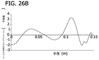
センサデータから得られる境界条件を用いて、クランプ条件から得られる境界条件とウエハWの特性(例えば、シリコンの材料特性)を組み合わせると、プロセッサ351は、ウエハのナノトポロジーの予測を含むウエハ形状を予測するように、ウエハの有限要素分析を行う。有限要素分析において、プロセッサ351によって予測されるウエハWの形状は、未加工ウエハのプロファイルである。研削プロセスは、典型的には、半径方向の対称性を示すナノトポロジーの特徴をもたらすので、未加工ウエハのプロファイルは、ウエハの中心から距離の関数として変形に関して表され得る。センサデータを用いた有限要素分析によって予測される未加工ウエハのプロファイルの1つの例は図に示される。
Using the boundary condition obtained from the sensor data, combining the boundary condition obtained from the clamping condition and the properties of the wafer W (eg, material properties of silicon), the
1つの実施形態において、変形したウエハ形状は、有限要素分析を用いて以下のように計算される。所定のメッシュは、シェル要素を用いて、この分析のために特定される。1つのメッシュの詳細は、図25Aに示される。ウエハの変形は、ウエハのクランプ角度、砥石の傾斜およびシフトに依存して、RまたはLのB−リングセンサにおいて、より可能性があるということを念頭に置くべきである。さらに大きい変形は、NT悪化とのさらに強い相関を有する傾向がある。従って、この効果を得るように、2つの測定値(reading)RおよびLのより高い方を両方の場所に適用する。静水圧パッドによるウエハクランプは、基本的な剛性(fundamental stiffness)の境界条件を用いて、もたらされる。研磨後のNTは、通常、10秒未満で計算される。研削砥石の外縁に沿ったウエハの変位(displacement)が考慮される(図25Bにおける弧ABC(arc ABC))。ウエハの中心から延在している全ての半径rについて、円弧に沿った2つの位置がある。これらの2つの位置における変位は、有限要素分析の結果に基づいて求めることができるおよびその半径における平均の変位を得るように平均化できる。平均の変位は、未加工プロファイル曲線としてプロットできる(図26A)。従って、未加工プロファイル曲線からの測定値は、フィルタ処理されたプロファイル曲線をもたらすように、空間フィルタを通過する(図26)。 In one embodiment, the deformed wafer shape is calculated using finite element analysis as follows. A given mesh is identified for this analysis using shell elements. Details of one mesh are shown in FIG. 25A. It should be borne in mind that wafer deformation is more likely in R or L B-ring sensors, depending on wafer clamping angle, wheel tilt and shift . Larger deformations tend to have a stronger correlation with NT degradation. Therefore, to obtain this effect, the higher of the two readings R and L is applied to both locations. Wafer clamping with a hydrostatic pad is effected using a fundamental stiffness boundary condition. NT after polishing is usually calculated in less than 10 seconds. Displacement of the wafer along the outer edge of the grinding wheel (displacement) is taken into account (the arc in FIG. 25B ABC (arc ABC)). For all radii r extending from the center of the wafer, there are two positions along the arc. The displacement at these two locations can be determined based on the results of the finite element analysis and can be averaged to obtain an average displacement at that radius. The average displacement can be plotted as a raw profile curve (FIG. 26A). Thus, the measurement from the raw profile curve passes through the spatial filter to yield a filtered profile curve (FIG. 26).
当業者に当然のことながら、研削後に、通常、付加的なウエハ処理工程がある。例えば、ウエハを、一般的に、研削後に研磨する。さらに、ナノトポロジー生成量は、研削した後ではないが仕上段階の処理工程(典型的には、ウエハのナノトポロジーを変化させる)が完了した後のナノトポロジーによって求められる。従って、本発明の1つの実施形態において、プロセッサ351は、有限要素分析から得られる未加工ウエハのプロファイルを用いて、1以上の仕上段階の処理工程後にウエハナノトポロジーがどうなり得るか予測するのに作動できる。
As will be appreciated by those skilled in the art, there are usually additional wafer processing steps after grinding. For example, a wafer is typically polished after grinding. Further, the amount of nanotopology generated is determined by the nanotopology after completion of the finishing process (typically changing the nanotopology of the wafer), but not after grinding. Thus, in one embodiment of the present invention, the
1以上の仕上段階の処理工程(例えば、研磨)後のウエハプロファイルを予測するように、例えば、空間フィルタは、未加工ウエハのプロファイルに適用できる。当業者は、この種の空間フィルタ処理を行うのに適用できる様々なウエハの欠陥/収率の管理ソフトウェアツールを知っている。いくつかの例は、SiGlaz of Santa ClaraからIntelligent Defect Analysis Software;Zenpire of Palo Alto、CAからiFAB software;Galaxy Semiconductor Inc. − USA of Waltham、MAからExaminator software;およびKnights Technology of Sunnyvale、CA.から Yieldmanager softwareを含む。フィルタ処理されたウエハプロファイルは、ナノトポロジーが更に処理された後にどうなり得るかの代表例である。フィルタ処理されたウエハプロファイルの1つの例は、図26bに示される。有限要素分析から得られる未加工ウエハのプロファイルを、多くのウエハのための仕上段階の処理後(例えば、研磨後)の実際のナノトポロジー測定(例えば、ナノマッパー(登録商標))と比較することにより、有限要素分析に用いるパラメータ(例えば、静水圧クランプに関した境界条件)は、より良い相関のために微調整できる。 For example, a spatial filter can be applied to a raw wafer profile so as to predict a wafer profile after one or more finishing stage processing steps (eg, polishing). Those skilled in the art are aware of various wafer defect / yield management software tools that can be applied to perform this type of spatial filtering. Some examples include SiGLof of Santa Clara to Intelligent Defect Analysis Software; Zenpipe of Palo Alto, CA to iFAB software; Galaxy Semiconductor Inc. -USA of Waltham, MA to Examiner software; and Knights Technology of Sunnyvale, CA. To Yield manager software. The filtered wafer profile is a representative example of what can happen after the nanotopology is further processed. One example of a filtered wafer profile is shown in FIG. 26b. By comparing the raw wafer profile obtained from finite element analysis to the actual nanotopology measurements (eg, NanoMapper®) after finishing (eg, after polishing) processing for many wafers The parameters used for finite element analysis (eg, boundary conditions for hydrostatic clamping) can be fine-tuned for better correlation .
さらに、プロセッサ351は、センサからセンサデータを受信しおよびセンサデータからワークピースのナノトポロジーを評価するように作動できる。1つの実施形態において、プロセッサは、悪いナノトポロジー評価に応じて改善作業を実施するように、必要に応じて、情報355(例えば、予測されたワークピースのNT)を提供するように作動できる(例えば、1以上のウエハプロファイルが、仕様または他の所定基準に適合しない場合にプロセッサによって求められるように)。その最も簡単な形態において、改善作業を対象とした情報355は、調整がなされるべきであるおよび/または研削プロセスが注意を必要とする1以上の人間操作者(例えば、プロセスエンジニア)を対象とした信号を出力することを含んでよい。プロセッサ351からの信号に応じて、人間操作者は、研削盤の性能を改善するように、研削盤の位置合わせ(例えば、研削砥石の水平傾斜に対応する少なくとも1つの角度、研削砥石の垂直傾斜に対応する角度、研削砥石同士の間のシフト)および/または静水圧パッドのポケットに供給される流体の圧力を調整できる。代替的にまたは追加的に、操作者は、研削盤の初期設定(例えば、設定のための親指の法則)を調整することによって、位置合わせを調整できる。プロセッサ351は、可変の研削プロセスを調整することを含むいくつかの改善作業を実施するように、他の情報355も提供できる。例えば、プロセッサ351は、センサデータに応じて研削砥石および/または静水圧パッドのうちの少なくとも1つの位置または適用についての調整、および/またはポケット313に供給される流体の圧力を調整することによるウエハに対するクランプ力の中心についての調整を示す情報355を提供するように作動できる。同様に、プロセッサ351は、研削盤を再整列するように、研削砥石9および静水圧パッド305の少なくとも1つの位置を調整するのに用いる一組のアクチュエータ(図示せず)を制御するように操作者の入力に応答できる。
Further, the
本発明に従って半導体ウエハを処理する方法の1つの実施形態において、上述したナノトポロジー評価システム301を有する両面研削盤内に半導体ウエハWを装填する。ウエハWの実際の研削は、本明細書での記載を除き、従来の様式で進行する。1以上のセンサ303は、研削プロセスの間において、ウエハWの変形を示しおよびウエハの有限要素構造分析のための1以上の境界条件を得るのに使用可能なデータを収集する。例えば、上述したナノトポロジー評価システム301のセンサ303は、ウエハWの表面とセンサとの間の複数の距離測定を収集する。さらに、評価システム301のセンサ303は、上述したように、ウエハの異なる部分から、研削盤要素に関する様々な位置において、同時にデータを収集する。
In one embodiment of a method for processing a semiconductor wafer according to the present invention, the semiconductor wafer W is loaded into a double-sided grinding machine having the
1つの実施形態において、センサは、B−リング欠陥に関連するワークピースの一部における距離に関して、ワークピースの2つの表面のずれを測定し、プロセッサ351は、センサからこのような距離データを受信し、受信したセンサデータから、ワークピースナノトポロジーにおけるB−リング欠陥を評価するように作動できる。別の実施形態において、センサは、C−マーク欠陥に関連するワークピースの一部分における距離に関して、ワークピースの2つの表面のずれを測定し、プロセッサ351は、センサから、このような距離データを受信し、受信したセンサデータからワークピースナノトポロジーにおけるC−マーク欠陥を評価するように作動できる。
In one embodiment, the sensor, B- respect to the distance in the part of the work piece to be associated with the ring defect, measuring the displacement of the two surfaces of the workpiece, the
センサ303は、センサデータをプロセッサ351に伝送し、該プロセッサ351は、センサデータを受信および処理する。センサ303からの出力は、図24に示すように、必要に応じて記録および/または図示される(研削中および/または研削後)。センサデータを、ウエハWのナノトポロジーを評価するのに用いる。方法の1つの実施形態において、プロセッサ351は、ウエハWのナノトポロジーを評価するように、研削プロセスにおける時間からセンサデータを記録する。例えば、図24は、両面研削プロセスサイクルの工程361、363、365、367、369と同時にプロットされる各々のセンサの時間変化出力を示す。プロセッサ351は、各々のセンサから一組の同時データを得るように、プロセスサイクルにおける所定時間(例えば、図24における矢印357により示される時間)において、センサ303からの出力を記録する。プロセッサ351は、ウエハWの有限要素構造分析を行うための境界条件を得るように、その組のデータを用いる。
The
プロセッサ351は、センサから得られる境界条件、および任意の他の境界条件(例えば、クランプ条件の情報から得られる境界条件)を用いて、ウエハの有限要素分析を行う(図25A)。有限要素分析を、未加工ナノトポロジーウエハプロファイルを生じるように用いる(図26B)。上述した空間フィルタを、必要に応じて、仕上段階の処理工程後(例えば、研磨後)にウエハWの生じ得るナノトポロジーを予測するように、未加工ウエハのプロファイルに適用する。
The
プロセッサ351は、ナノトポロジー要求について、研削盤の性能を評価するように、未加工ウエハのプロファイルおよび/またはフィルタ処理されたウエハプロファイルを再検討する。この評価は、研削盤ナノトポロジー性能が所定の基準を満たすかどうかを求めるように、バッチにおける他のウエハのために未加工ウエハのプロファイルおよび/またはフィルタ処理されたウエハププロファイルを考慮できる。プロセッサ351が、研削盤がナノトポロジー基準を満たさないということを求めた場合に、プロセッサは、改善作業を始める。1つの実施形態において、改善作業は、研削装置が注意を必要とする1以上の人間操作者に信号を送ることを含む。従って、人間の操作者は、上述したように、研削盤装置の位置合わせを調整するおよび/またはクランプの中心を調整する。別の実施形態において、プロセッサ351は、悪いナノトポロジー評価および操作者入力に応じて、改善作業を実施する。例えば、プロセッサ351は、プロセッサの制御下において操作者入力に応じて1以上のアクチュエータを用いて、クランプの中心を調整するおよび/または研削盤の位置合わせを調整するように、ウエハWの1以上の部分に適用される静水圧量を調整できる。
The
別の実施形態において、改善作業は、次のワークピースの研削を調整することを含む。例えば、研削盤は、第1ワークピースを研削しおよび次いで第1ワークピースを研削した後に第2ワークピースを研削するように作動できる。プロセッサ351は、センサからデータを受信しおよびセンサデータから第1ワークピースのナノトポロジーを評価するのに作動できる。従って、プロセッサ351は、第2ワークピースのような次のワークピースを研削する場合に用いるためのセンサデータに応じて、研削砥石および/または静水圧パッドの少なくとも1つの位置に対する調整を示す情報355を提供するように作動できる。ワークピースが複数のウエハのカセットである状況において、有限要素分析を、カセットにおける各々のウエハに対して行うことができ、ウエハのカセット全体を研削するまで待つ必要がない。従って、設定値が適切でない場合およびNT欠陥を1以上のウエハ内において検出する場合に、カセットにおける他のウエハが、いくらかの形態の介入なしに、さらに大きな収率損失をもたらす類似または同じ欠陥を有することはあり得る。本発明の1つの実施形態に従って、操作者は、カセットにおける全てのウエハからフィードバックを得るように待つ必要がなく、多量の収率損失を避ける。従って、研磨中における研磨後のNT欠陥の信頼性のある予測が提供される。このような予測は、次のウエハおよびカセットのための研削盤設定値を最適化して、次のウエハの研磨後のナノトポロジー欠陥を最小化するように操作者を支援する。
In another embodiment, the improvement operation includes adjusting the grinding of the next workpiece . For example, grinding machine, operable to grind a second workpiece to a first workpiece after grinding the ground to and then the first workpiece. The
図27は、ナノマッパーによって求められるように、特定のウエハのための本発明の1つの実施形態に従って予測されるプロファイルを示し、研磨後に、その同じウエハのための平均的な半径の変位を示すグラフである。実線は、本発明の1つの実施形態に従って、有限要素分析に基づいてウエハの予測されるプロファイルの1つの例を示す。破線は、ウエハを分析したナノマッパーからのデータに基づいてプロファイルを示す。図28は、多くのウエハの水平軸にプロットされている予測B−リング値と、垂直軸にプロットされている実際のB−リング値との間の相関を示すグラフであり、相関係数は、R=0.9である。 Figure 27 is, as can be determined by Nanomappa, shows a profile that is predicted according to one embodiment of the present invention for a particular wafer, the research Migakugo shows an average radius of the displacement for the same wafer It is a graph. The solid line shows one example of the predicted profile of the wafer based on finite element analysis, according to one embodiment of the invention. The dashed line shows the profile based on data from the nanomapper that analyzed the wafer. FIG. 28 is a graph showing the correlation between the predicted B-ring value plotted on the horizontal axis of many wafers and the actual B-ring value plotted on the vertical axis. , R = 0.9.
本発明の方法は、研削盤のナノトポロジー性能に対する素早いフィードバックを提供する。例えば、ウエハナノトポロジーの評価は、ウエハの研削サイクルが完了する前に始めることができる。さらに、ナノトポロジーフィードバックは、研磨前に得られる。対照的に、多くの従来のナノトポロジーフィードバックシステムは、ウエハナノトポロジーを測定するように、レーザー検査を用いる。これらのシステムは、典型的には、反射的な表面を欠く非研磨ウエハを有する使用に適合しない。本発明の方法を通じて得られる多くの他の利点は、この開示の観点から当業者によって認識される。 The method of the present invention provides quick feedback on the nanotopological performance of the grinder. For example, evaluation of the wafer nanotopology can begin before the wafer grinding cycle is completed. Furthermore, nanotopology feedback is obtained before polishing. In contrast, many conventional nanotopology feedback systems use laser inspection to measure wafer nanotopology. These systems are typically not suitable for use with unpolished wafers that lack a reflective surface. Many other advantages obtained through the method of the present invention will be recognized by those skilled in the art in light of this disclosure.
上述した方法において、センサ303は、研削盤操作中に、実質的に連続してデータを収集する。しかしながら、研削が完了した後、ウエハがまだ研削盤内にある間に、データをセンサから収集できることを理解されたい。さらに、センサ303は、本発明の技術的範囲から逸脱せずに、時間内において断続的または一点において測定を行ってよい。同様に、本発明の技術的範囲から逸脱せずに、研削操作が完了した後および/またはウエハが研削盤から取り出された後に、センサデータの処理が始まるまたは続くことができる。
In the method described above, the
また、上述したナノトポロジーシステムの実施形態は、ウエハを両面研削盤内で垂直に保持しつつ、ウエハのナノトポロジーを評価することを示しているが、本発明の技術的範囲から逸脱せずに、異なる方向(例えば、水平方向)に保持されたウエハのナノトポロジーを評価するように、ナノトポロジー評価システムを使用できることを理解されたい。 Further, embodiments of the nanotopology system described above, while holding the wafer vertically in both grinder in, you are shown to evaluate the nanotopology of the wafer but, without departing from the scope of the present invention in different directions (e.g., horizontal direction) so as to evaluate the nanotopology of the wafer held on, it is to be understood that can use the nanotopology evaluation system.
本明細書に記載されたナノトポロジー評価システムについての実施形態では、ナノトポロジーを評価するためにウエハごとに有限要素分析を行っているが、当業者であれば、プロセッサが、実際に有限要素構造分析を行わずにナノトポロジーを評価できる基準を開発するために、多くのこのような有限要素分析からの経験的データを利用できることを認識するだろう。例えば、研削盤内におけるウエハのセンサデータが、有限要素分析を行った別のウエハのセンサデータと十分に似ている場合には、研削盤内のウエハの有限要素分析を実際に行わずに研削盤内のウエハのナノトポロジーを評価するために、これまでの有限要素分析結果を用いることができる。データベースおよび学習ルーチンは、この処理を拡大するのに使用でき、これにより、プロセッサが有限要素分析を行う場合を減少または排除できる。ナノトポロジー評価システムに熟練した人間オペレータは、センサ出力のグラフまたは他の表示を見ることによってナノトポロジー欠陥を示すサインを見分ける能力、および、本発明の技術的範囲から逸脱せずに、是正措置を手動で実施する能力が身につくことも検討される。 In the embodiment of the nanotopology evaluation system described herein, although Life has a finite element analysis for each wafer in order to evaluate the nanotopology, those skilled in the art, the processor is actually finite in order to develop the criteria that you can evaluate the nano-topology without the element structure analysis, would recognize that the available empirical data from a number of such finite element analysis. For example, a wafer of the back Nsadeta in the grinding machine in is, if another wafer is similar in the back and enough Nsadeta performing the finite element analysis, Ken without actually performing the finite element analysis of the wafer in the grinding machine to evaluate the wafer nanotopology of the cutting machine, it is possible to use a finite element analysis so far. Databases and learning routines can be used to scale this process , thereby reducing or eliminating the case where the processor performs finite element analysis. Human operator skilled in nanotopology evaluation system, the ability to distinguish sign indicating the nanotopology defects by viewing the graph or other display of the sensor output, and, without departing from the scope of the present invention, corrective action It is also considered to acquire the ability to carry out this manually.
さらに、ウエハごとにナノトポロジー評価を行うことは必須ではない。必要に応じて、ナノトポロジーは、本発明の技術的範囲から逸脱せずに、研削盤内で研削されたウエハのサブセット(例えば、品質管理のためのサンプル)について、本明細書に記載されるように評価できる。 Furthermore, it is not essential to perform the nanotopology evaluated every U Fine. Optionally, nanotopologies are described herein for a subset of wafers (eg, samples for quality control ) that have been ground in a grinder without departing from the scope of the present invention. Can be evaluated.
概略図の図29を参照すると、別の実施形態のウエハ研削盤を図示しており、一般に500で表される。ウエハ研削盤は、一般に、第1静水圧パッド506と、第1静水圧パッドとは反対に位置する第2静水圧パッド508を含む。ウエハ501(広義には、ワークピース)は、静水圧パッド506、508の間に配置されている。一対の研削砥石(図示せず)は、ウエハ研削盤内に含まれる。ウエハ研削盤は、上述したこれらの実施形態と類似していてもよい。しかしながら、図29のウエハ研削盤は、ウエハ研削盤で処理したウエハのNT悪化の軽減を支援するために、付加的な構成要素を含む。
Referring to Figure 29 of approximate schematic, and illustrates a wafer grinder another embodiment, generally denoted by 500. The wafer grinding machine generally includes a first
第1流量制御弁504は、第1静水圧パッド506に向かう水流を制御し、第2流量制御弁502は、第2静水圧パッド508に向かう水流を制御する。この実施形態において、パッド内の静水圧は、他のモードも検討されるが、水流よって制御される。
The first
流量制御弁502、504は、水流または水圧を制御できる適切な弁である。例えば、流量制御弁502、504は、グローブ弁、ボール弁、ゲート弁、ダイアフラム弁、ニードルバルブまたはそれらの任意の組み合わせであってよい。流量制御弁502、504は、適切なアクチュエータ(図示せず)で制御することができ、また、それらは別々に制御できる。
制御システム600は、ウエハ研削盤および流量制御弁502、504の操作を制御する。制御システム600は、プロセッサを有するコンピューターデバイス602と、1つ以上の形態のコンピューター可読媒体と、入力/出力デバイスとを含む。いくらかの実施形態において、コンピューターデバイス602のプロセッサは、流量制御弁502、504を制御するように作動できる。制御システム600は、研削砥石によって使用される電流量を測定するように作動できる。制御システム600は、研削砥石によって使用される電流を直接測定できるか、または、研削砥石によって使用される電流を測定する分離した監視デバイス(図示せず)からの信号または他の通信を受信できる。
The
研削砥石によって使用される電流量は、研削操作の現在の段階を表している。例えば、図30に示すように、研削砥石がウエハ501と最初に接触すると、研削砥石によって引き込まれる電流は、540で示した残留状態と比較して、550で示した初期状態においてわずかに増加する。図30は、研削操作中の各研削砥石によって引き込まれる電流を示す。電流引き込みは、560で示した部分に沿って示されるように、研削砥石がウエハ501を掴もうとすると増加し続ける。この段階の間に、ウエハ501から比較的少量の材料が除去される。電流引き込みが、570で示したセクションおいてそのピークに達したとき、ウエハ501から除去される材料の量は増加する。電流引き込みは、このピークレベルにとどまり、材料の大部分が研削砥石によってウエハ501から除去される。580で示したスパークアウト段階(その間に研削砥石を後退させ始める)では、電流引き込みは、急速に低下する。研削砥石が完全に格納された後、電流引き込みは低下して、590で示した残留レベルに戻る。 The amount of current by the grinding wheel Ru is used represents the current stage of the grinding operation. For example, as shown in FIG. 30, when the grinding wheel first contacts the wafer 501, the current Ru drawn by the grinding wheel, as compared with the residual state shown at 540, slightly in the initial state shown in 550 To increase. FIG. 30 shows the current drawn by each grinding wheel during the grinding operation. Current draw continues to increase as the grinding wheel attempts to grab the wafer 501 as shown along the portion indicated at 560. During this stage, a relatively small amount of material is removed from the wafer 501. Current draw, when reached in section Oite the peak indicated at 570, the amount of material removed from the wafer 501 is increased. Current draw is Ri Todoma this peak level, most of the material is removed from the wafer 501 by the grinding wheel. In the spark-out phase indicated at 580 ( while the grinding wheel begins to retract ) , the current draw decreases rapidly. After the grinding wheel has been fully retracted, the current draw is reduced, back to the residual level indicated at 590.
コンピューターデバイス602は、研削操作の現在の段階を予測(すなわち、検出または決定)するために、監視された、または感知された研削砥石の電流引き込みを用いる。コンピューターデバイス602は、パターン検出ソフトウェアプログラムの支援によってこの予測を行う。パターン検出ソフトウェアプログラムは、コンピューターデバイス602上の1つ以上の形態のコンピューター可読媒体に蓄積されたコンピューター実行可能命令を含む。コンピューター実行可能命令は、コンピューターデバイス602のプロセッサによって実行される。
制御システム600は、パターン検出ソフトウェアによって決められた研削段階に基づいて、流量制御弁502、504を用いて、静水圧パッド506、508内の圧力を制御するように操作可能である。NT悪化を最小限にするように、制御システム600は、研削段階中における研削プロセスの開始時および終了時に、静水圧パッド内の圧力を増加する。これらの研削段階では、研削砥石の電流引き込みは最も低くなる。従って、制御システム600は、流量制御弁が静水圧パッド506、508への水の流入速度を増加させて、それにより静水圧パッド内の圧力を増加させるように、流量制御弁502、504を制御する。
ウエハ501から材料の大部分を除去する(1つまたは複数の)研削段階中に、制御システム600は、静水圧パッド506、508への水の流入速度を減少し、それにより静水圧パッド内の圧力を減少するように、流量制御弁502、504を制御する。この研削段階において、(2つの)研削砥石は、それらの間でウエハ501を支持し、そしてウエハを掴む。この研削段階中に静水圧パッド506、508内の圧力を減少することによって、ウエハが受ける弾性変形の量は、劇的に減少または排除される。ウエハ501内での弾性変形のこのような減少または排除は、ウエハ表面に低減したNTをもたらす。
From the wafer 501 to remove most of the material in (one or more) grinding stage, the
操作中、制御システム600は、ブロック610において、パターン検出ソフトウェアを用いて研削段階を検出する方法(すなわち決定する方法)を実行する。ブロック620では、ブロック610においてパターン検出ソフトウェアで検出された研削段階に基づいて、流速の変化を計算する。制御システム600は、ブロック630で、流量制御弁502、504を制御することによってこれらの変化を適用する。このように、制御システム600は、静水圧を調節するように作動できる。
Misao Sakuchu,
ウエハ501をパッド間に初めにクランプするのに、制御システム600は、静水圧パッド506、508において第1静水圧を確立する別の方法を行うように作動できる。この方法では、ウエハ501を、実質的に垂直な平面内で保持する。次いで、ウエハ501の研削中に、流量制御弁502、504により、静水圧パッド506、508における静水圧を第1圧力よりも低い第2静水圧まで減少させる。ウエハ501の研削中に、ウエハ501を、研削砥石によって実質的にクランプできる。次いで、ウエハをクランプし、従ってウエハ501におけるナノトポロジーを改善するように、静水圧を、第3静水圧まで増加する。第3静水圧は、第1静水圧と実質的に同じであってよい。
In order to initially clamp the wafer 501 between the pads, the
別の方法においては、制御システム600は、ウエハをクランプする段階と、ウエハを研削する段階と、ウエハを研削砥石との接触から離す段階と、を含む方法を行う。ウエハは、実質的に垂直な平面内で保持される。パターン検出ソフトウェアを使用して研削操作の各々の段階を検出し、各々の段階における静水圧を変えてウエハに適用されるクランプ圧力を変化させ、それにより処理されたウエハのナノトポロジーを改善する。圧力を変化させる他の方法も検討できるが、本実施形態の静水圧は、流量制御弁502、504を通過する流速を変えることによって変化させる。例示的な実施形態では、圧力は、研削段階で減少させる。他の実施形態では、圧力は、研削段階中に増加させる。
Oite to another method, the
第1組のウエハと第2組のウエハの表面を測定することによって、2つのデータセットを得た。試験されるウエハは、入口および出口のマークまたは他の類似した欠陥がなかった。第1組のウエハを従来の方法(すなわち、プロセスレコード(process of record)またはPOR)に従って研削し、静水圧は研削段階中に変えなかった。第2組のウエハを、図29の実施形態に従って研削し、静水圧を研削段階中に増加させた。試験したウエハの表面を、表面の部分(例えば、10mm×10mmの部分)のためにしきい値の高さ平均(すなわち、THA1010測定標準)に従って測定した。THA1010測定標準に従って行われた測定は、ウエハの表面の部分内において、最大ピークバレー垂直距離を表す。多数のこのような測定を、異なる部分におけるウエハの表面を横切って行う(部分は重なり得るけれども)。THA1010測定標準は、ウエハ表面のナノトポロジーを評価するのに用いる既知の測定標準である。標準を用いると、数が少ないほど、ウエハ表面のナノトポロジーは良好であった。 Two data sets were obtained by measuring the surface of the first set of wafers and the second set of wafers. The wafers tested were free of entry and exit marks or other similar defects. A first set of wafers was ground according to conventional methods (ie, process of record or POR) and the hydrostatic pressure was not changed during the grinding phase . A second set of wafers was ground in accordance with the embodiment of FIG. 29, increased hydrostatic pressure during the grinding stage. The surface of the tested wafer was measured according to a threshold height average (ie, THA 1010 measurement standard) for a portion of the surface (eg, a 10 mm × 10 mm portion). Measurements made in accordance with the THA 1010 measurement standard represent the maximum peak valley vertical distance within a portion of the surface of the wafer. A number of such measurements are made across the surface of the wafer in different parts (although parts can overlap). The THA1010 measurement standard is a known measurement standard used to evaluate the nanotopology of the wafer surface. Using the standard, the smaller the number, the better the nanotopology of the wafer surface.
図31は、両方のデータセットのためのTHA1010測定の規格化された分布を示すグラフである。第1データセットは、規格化されたTHA1010 PORのことを言い、第2データセットは、規格化された THA1010 Low Prのことを言う。各々のデータセットに対する測定を規格化した(すなわち、公約数で割った)。グラフにおけるデータポイントの各々の1つのy軸は、別個のデータポイントのx軸と等しいまたはそれより少ない測定値のパーセントを表す。さらに、実線は、第1データセットのために95%の信頼区間の境界を表す。破線は、第2データセットのために95%の信頼区間の境界を表す。 FIG. 31 is a graph showing the normalized distribution of THA1010 measurements for both data sets. The first data set refers to the standardized THA1010 POR , and the second data set refers to the standardized THA1010 Low Pr. The measurements for each data set were normalized (ie divided by the common divisor). One y-axis of each of the data points in the graph represents a percentage of the measurement that is equal to or less than the x-axis of the distinct data point. Furthermore, the solid line represents the boundary of the 95% confidence interval for the first data set. Dashed lines represent 95% confidence interval boundaries for the second data set.
図32は、試験したウエハの表面における規格化されたしきい値の高さ領域の測定を示すボックスプロット表である。表は、図31の2つのデータセットのボックスプロットを示し、各々のデータセットのために、表は、それぞれ、最小、第1四分位数、中間、第3四分位数および最大を示す。 FIG. 32 is a box plot table showing the measurement of the normalized threshold height region on the surface of the tested wafer. Table shows the box plot of two data sets in Figure 31, for data sets each, tables, respectively, minimum, first quartile, the intermediate, third quartile and maximum Show.
図31および32は、図29の実施形態に従って研削したウエハの表面が、PORに従って研削したウエハよりも顕著に低いピークバレー値を有することを示す。従って、図29の実施形態に従って研削したウエハの表面は、PORに従って研削したウエハの表面と比較して、改善したナノトポロジーを有する。例えば、図29のプロセスに従って研削したウエハは、0.6346の規格化した平均THA1010を有するが、PORに従って研削したウエハは、0.6738の規格化した平均THA1010を有する。同様に、標準誤差は、POR(標準誤差=0.09956)に従って研削したウエハと比較して、図29に従って(標準誤差=0.09826)研削したウエハについて減少する 31 and 32 show that the surface of a wafer ground according to the embodiment of FIG. 29 has a significantly lower peak valley value than a wafer ground according to POR. Thus, the surface of a wafer ground according to the embodiment of FIG. 29 has an improved nanotopology compared to the surface of a wafer ground according to POR. For example, a wafer ground according to the process of FIG. 29 has a normalized average THA 1010 of 0.6346, while a wafer ground according to POR has a normalized average THA 1010 of 0.6738. Similarly, the standard error decreases for a wafer ground according to FIG. 29 (standard error = 0.09826) compared to a wafer ground according to POR (standard error = 0.09956).
さらに、図32のボックスプロット表は、図29に従って研削したウエハの規格化されたピークバレー測定値が、PORのそれらと比較してより狭い範囲において分布することを示す。明確に示されるように、第2データセットの第1および第3の四分位数(すなわち、Low Pr)は、第1データセットのそれら(すなわち、POR Pr)よりも更に狭い間隔である。さらに、第2データセットの最大および最小は、第1データセットの最大および最小よりも更に低い値を有する。 In addition, the box plot table of FIG. 32 shows that the normalized peak valley measurements of wafers ground according to FIG. 29 are distributed in a narrower range compared to those of POR. As clearly shown, the first and third quartiles (ie, Low Pr) of the second data set are more closely spaced than those of the first data set (ie, POR Pr). Furthermore, the maximum and minimum of the second data set have values that are even lower than the maximum and minimum of the first data set.
本発明またはその好ましい実施形態の要素を導入するときに、冠詞「a」、「an」、「the」および「said」は、1つ以上の要素があることを意味するように意図している。用語「comprising」、「including」および「having」は、包含的でありかつ示された要素以外の追加的な要素があってよいことを意味することを意図している。 When introducing elements of the present invention or the preferred embodiment, the articles "a", "an", "the" and "said" are intended to mean that there are one or more of the elements . The term "comprising", "including" and "having" are intended to mean that there may be additional elements other than inclusive and is and the elements shown.
本発明の技術的範囲から逸脱することなく、上記のものに様々な変化を行うことができるので、上述の記載に含まれおよび添付の図面に図示された全ての事項は、例示と解釈されるべきであり、制限する意味ではないことを意図している。 Without departing from the scope of the present invention, it is possible to perform various changes to the above, all matter shown figure contained and the accompanying drawings in the foregoing description may be interpreted as illustrative Should be meant and not meant to be limiting .
本明細書の開示内容は、以下の態様を含み得る。 The disclosure of the present specification may include the following aspects.
(態様1)(Aspect 1)
一対の研削砥石と、その中に静水圧を有する一対の静水圧パッドとの間にウエハを保持するタイプの両面研削盤を用いて半導体ウエハを処理する方法であって、研削盤は、研削盤によって引き込まれた電流を検出するためのパターン検出ソフトウェアを含むプロセッサを含んでおり、該方法は、 A method of processing a semiconductor wafer using a double-sided grinding machine of a type that holds a wafer between a pair of grinding wheels and a pair of hydrostatic pressure pads having a hydrostatic pressure therein, wherein the grinding machine is a grinding machine Including a processor including pattern detection software for detecting current drawn by the method,
ウエハをクランプする段階と、 Clamping the wafer;
ウエハを研削する段階と、 Grinding the wafer;
ウエハを研削砥石との接触から離す段階と、 Separating the wafer from contact with the grinding wheel;
各々の段階を検出するためのソフトウェアを使用し、各々の段階における静水圧を変えて、ウエハに適用されるクランプ圧力を変え、それにより処理したウエハのナノトポロジーを改善する段階と、の複数の段階を含む方法。 Using software for detecting each stage, changing the hydrostatic pressure in each stage, changing the clamping pressure applied to the wafer, thereby improving the nanotopology of the processed wafer, A method comprising stages.
(態様2)(Aspect 2)
流量制御弁を通過する流速を変えることによって静水圧を変える、態様1に記載の方法。 The method of
(態様3)(Aspect 3)
各々の段階を検出するために、研削盤によって引き込まれる電流をパターン検出ソフトウェアで測定する、態様1に記載の方法。 The method of
(態様4)(Aspect 4)
研削段階において、静水圧を低下させることを更に含む、態様1に記載の方法。 The method of
(態様5)(Aspect 5)
研削段階において、静水圧を上昇させることを更に含む、態様1に記載の方法。 The method of
(態様6)(Aspect 6)
研削操作中に一対の研削砥石と一対の静水圧パッドとの間にウエハを保持するタイプの両面研削盤を用いて半導体ウエハを処理する方法であって、該方法は、 A method of processing a semiconductor wafer using a double-sided grinder of a type that holds a wafer between a pair of grinding wheels and a pair of hydrostatic pressure pads during a grinding operation, the method comprising:
研削操作の第1段階において、静水圧パッド内に第1静水圧を確立してウエハを最初にクランプすることと、 Establishing a first hydrostatic pressure in the hydrostatic pressure pad and first clamping the wafer in a first stage of the grinding operation;
研削操作の第2段階でウエハを研削する間に、第1圧力よりも低い第2静水圧まで静水圧を低下させることと、 Reducing the hydrostatic pressure to a second hydrostatic pressure lower than the first pressure while grinding the wafer in the second stage of the grinding operation;
研削操作の第3段階において第3静水圧まで静水圧を上昇させてウエハをクランプし、これにより処理されたウエハのナノトポロジーを改善することと、を含む方法。 Increasing the hydrostatic pressure to a third hydrostatic pressure in a third stage of the grinding operation to clamp the wafer, thereby improving the nanotopology of the processed wafer.
(態様7)(Aspect 7)
第3静水圧は第1静水圧と実質的に等しい、態様6に記載の方法。 The method of
(態様8)(Aspect 8)
ウエハの研削中に、研削砥石によってウエハを実質的にクランプする、態様6に記載の方法。 The method of
(態様9)(Aspect 9)
静水圧を、流量制御弁の使用によって変える、態様6に記載の方法。 The method of
(態様10)(Aspect 10)
ウエハを、実質的に垂直な平面内で保持する、態様6に記載の方法。 The method of
(態様11)(Aspect 11)
両面研削盤の研削砥石によって使用される電流量を測定することを更に含む、態様6に記載の方法。 The method of
(態様12)(Aspect 12)
両面研削盤の研削砥石によって使用される、測定された電流量に基づいて、研削操作の段階を決めることを更に含む、態様11に記載の方法。 12. The method of
(態様13)(Aspect 13)
測定された電流が残留状態から初期状態まで増加したときに、研削操作の段階が第1段階であると決めることを更に含む、態様12に記載の方法。 13. The method of aspect 12, further comprising determining that the stage of the grinding operation is the first stage when the measured current increases from a residual state to an initial state.
(態様14)(Aspect 14)
測定された電流がそのピークレベルであるときに、研削操作の段階が第2段階であると決めることを更に含む、態様12に記載の方法。 13. The method of aspect 12, further comprising determining that the stage of the grinding operation is the second stage when the measured current is at its peak level.
(態様15)(Aspect 15)
測定された電流がそのピークレベルから減少したときに、研削操作の段階が第3段階であると決めることを更に含む、態様14に記載の方法。 15. The method of
(態様16)(Aspect 16)
一対の研削砥石と、プロセッサと、一対の静水圧パッドとを含む両面研削盤であって、 A double-side grinding machine including a pair of grinding wheels, a processor, and a pair of hydrostatic pressure pads,
研削砥石と静水圧パッドとは、ほぼ平坦なウエハを、一対の研削砥石の間に配置されているウエハの第1部分と一対の静水圧パッドの間に配置されているウエハの第2部分とが同一平面内で保持されるように操作可能であり、 The grinding wheel and the hydrostatic pressure pad include a substantially flat wafer, a first portion of the wafer disposed between the pair of grinding wheels, and a second portion of the wafer disposed between the pair of hydrostatic pressure pads. Can be operated to be held in the same plane,
静水圧パッドは、静水圧を維持するように静水圧パッドを通過して流れる水を含み、 The hydrostatic pad includes water that flows through the hydrostatic pad to maintain the hydrostatic pressure,
研削盤は、パッドを通過する水の流速を制御するための、それにより静水圧を制御するための、流量制御弁を更に含み、 The grinder further includes a flow control valve for controlling the flow rate of water through the pad, thereby controlling the hydrostatic pressure,
流量制御弁は、プロセッサによって制御される、両面研削盤。 The flow control valve is a double-sided grinding machine controlled by a processor.
(態様17)(Aspect 17)
プロセッサが、研削プロセスの様々な段階を検出するためのパターン検出ソフトウェアを含んでおり、該プロセッサは、パターン検出ソフトウェアによって検出された段階に応じて、流量制御弁を通過する水の流速を制御するように動作可能である、態様16に記載の研削盤。 The processor includes pattern detection software for detecting various stages of the grinding process, the processor controlling the flow rate of water through the flow control valve in response to the stages detected by the pattern detection software. A grinder according to aspect 16, wherein the grinder is operable.
(態様18)(Aspect 18)
プロセッサが、研削砥石によって使用される電流量を測定するように動作可能である、態様17に記載の研削盤。 The grinder of aspect 17, wherein the processor is operable to measure the amount of current used by the grinding wheel.
(態様19)(Aspect 19)
パターン検出ソフトウェアは、研削砥石によって使用される、測定された電気量に基づいて段階を検出する、態様18に記載の研削盤。 The grinder according to aspect 18, wherein the pattern detection software detects the stage based on the measured electrical quantity used by the grinding wheel.
(態様20)(Aspect 20)
プロセッサは、パターン検出ソフトウェアが研削プロセスの研削段階を検出したときに、弁を通過する水の流速を増加するように流量制御弁を制御する、態様19に記載の研削盤。 The grinder of aspect 19, wherein the processor controls the flow control valve to increase the flow rate of water through the valve when the pattern detection software detects the grinding phase of the grinding process.
Claims (10)
研削操作の第1段階において、静水圧パッド内に第1静水圧を確立してウエハを最初にクランプすること、
両面研削盤の研削砥石によって使用される電流量を測定すること、
両面研削盤の研削砥石によって使用される、測定された電流量に基づいて、研削操作の3つの段階の1つを決定すること、
研削操作の第2段階でウエハを研削する間に、第1静水圧よりも低い第2静水圧まで静水圧を低下させること、および
研削操作の第3段階の間において、第3静水圧まで静水圧を上昇させて、静水圧パッドによりウエハをクランプし、それにより、処理されたウエハにおけるナノトポロジーを改善すること、を含み、
第1段階は、ウエハが静水圧パッドによってクランプされる最初の期間に対応し、
第2段階は、研削操作が除去する間のうち、最も多くの材料が除去される第2の期間に対応する、
方法。 A method of processing a semiconductor wafer using a double-sided grinder of the type that holds a wafer between a pair of grinding wheels and a pair of hydrostatic pressure pads during a grinding operation performed by a double-sided grinder, the method In the first stage of the grinding operation, establishing a first hydrostatic pressure in the hydrostatic pad and first clamping the wafer;
Measuring the amount of current used by the grinding wheel of a double-sided grinder,
Determining one of the three stages of the grinding operation based on the measured amount of current used by the grinding wheel of the double-side grinder;
Lowering the hydrostatic pressure to a second hydrostatic pressure lower than the first hydrostatic pressure while grinding the wafer in the second stage of the grinding operation, and static to the third hydrostatic pressure during the third stage of the grinding operation. Increasing the water pressure and clamping the wafer with a hydrostatic pressure pad, thereby improving the nanotopology in the processed wafer,
The first stage, the wafer corresponds to the first period which is clamped by hydrostatic pads,
The second stage corresponds to a second period during which most of the material is removed while the grinding operation is removed.
Method.
測定された電流がそのピークレベルから減少したとの決定に応じて、静水圧を増加する、請求項7に記載の方法。 Further determining that the stage of the grinding operation is the third stage when the measured current decreases from its peak level;
8. The method of claim 7, wherein the hydrostatic pressure is increased in response to determining that the measured current has decreased from its peak level.
研削砥石と静水圧パッドとが、一対の研削砥石の間に配置されたウエハの第1部分および一対の静水圧パッドの間に配置されたウエハの第2部分とを備えた平坦なウエハとを同一平面で保持するように作動でき、
プロセッサが、研削砥石によって使用される電流量を測定するように作動し、
静水圧パッドが、静水圧を維持するようにそこを通過して流れる水を含み、
流れ制御弁が、パッドを通過する水の流速を制御しそれにより静水圧を制御するように作動し、
プロセッサは、研削砥石によって使用される、測定された電気量に基づいて、切削プロセスの段階を検出するパターン検出ソフトウェアプログラムを実行し、
プロセッサは、パターン検出ソフトウェアプログラムによって検出された段階に応じて、流れ制御弁を通過する水の流速を制御するように作動する両面研削盤。 A double-side grinding machine including a pair of grinding wheels, a processor, a pair of hydrostatic pressure pads, and a flow control valve,
A grinding wheel and a hydrostatic pressure pad, and Tan wafer flat with a second portion of the arranged wafers between the first portion and a pair of hydrostatic pads disposed wafers between a pair of grinding wheels Can be held in the same plane,
The processor operates to measure the amount of current used by the grinding wheel;
A hydrostatic pad includes water flowing therethrough to maintain hydrostatic pressure;
A flow control valve operates to control the flow rate of water through the pad and thereby control the hydrostatic pressure;
The processor executes a pattern detection software program that detects the stage of the cutting process based on the measured electrical quantity used by the grinding wheel;
A double-sided grinding machine in which the processor is operative to control the flow rate of water passing through the flow control valve according to the stage detected by the pattern detection software program .
Applications Claiming Priority (3)
| Application Number | Priority Date | Filing Date | Title |
|---|---|---|---|
| US31791910P | 2010-03-26 | 2010-03-26 | |
| US61/317,919 | 2010-03-26 | ||
| PCT/IB2011/051152 WO2011117792A1 (en) | 2010-03-26 | 2011-03-18 | Hydrostatic pad pressure modulation in a simultaneous double side wafer grinder |
Publications (3)
| Publication Number | Publication Date |
|---|---|
| JP2013524484A JP2013524484A (en) | 2013-06-17 |
| JP2013524484A5 JP2013524484A5 (en) | 2015-10-15 |
| JP6013317B2 true JP6013317B2 (en) | 2016-10-25 |
Family
ID=44657008
Family Applications (1)
| Application Number | Title | Priority Date | Filing Date |
|---|---|---|---|
| JP2013500633A Active JP6013317B2 (en) | 2010-03-26 | 2011-03-18 | Hydrostatic pad pressure adjustment in simultaneous double-sided wafer grinder |
Country Status (8)
| Country | Link |
|---|---|
| US (1) | US8712575B2 (en) |
| EP (1) | EP2552644A4 (en) |
| JP (1) | JP6013317B2 (en) |
| KR (1) | KR101694574B1 (en) |
| CN (1) | CN102844151A (en) |
| SG (1) | SG184014A1 (en) |
| TW (1) | TWI520202B (en) |
| WO (1) | WO2011117792A1 (en) |
Families Citing this family (14)
| Publication number | Priority date | Publication date | Assignee | Title |
|---|---|---|---|---|
| US9358660B2 (en) | 2011-11-07 | 2016-06-07 | Taiwan Semiconductor Manufacturing Company, Ltd. | Grinding wheel design with elongated teeth arrangement |
| US9960088B2 (en) * | 2011-11-07 | 2018-05-01 | Taiwan Semiconductor Manufacturing Company, Ltd. | End point detection in grinding |
| JP6197580B2 (en) * | 2013-10-29 | 2017-09-20 | 株式会社Sumco | Double-side polishing machine for carrier plate and workpiece |
| CN105881213A (en) * | 2014-09-01 | 2016-08-24 | 曾庆明 | Precision double-face grinder controller |
| JP6285375B2 (en) * | 2015-02-17 | 2018-02-28 | 光洋機械工業株式会社 | Double-head surface grinding machine |
| JP6447472B2 (en) * | 2015-11-26 | 2019-01-09 | 株式会社Sumco | Wafer polishing method |
| CN108127560A (en) * | 2017-12-08 | 2018-06-08 | 中国兵器科学研究院宁波分院 | For the control system of the two-sided fast polishing of square optical element |
| JP6513174B2 (en) * | 2017-12-25 | 2019-05-15 | 信越半導体株式会社 | Design method of wafer holding carrier |
| JP7159861B2 (en) * | 2018-12-27 | 2022-10-25 | 株式会社Sumco | Double-headed grinding method |
| CN112930248B (en) * | 2019-04-01 | 2023-05-02 | 株式会社村田制作所 | Polishing agent supply device, polishing device, and polishing agent supply method |
| US11415971B2 (en) | 2020-02-10 | 2022-08-16 | Globalwafers Co., Ltd. | Systems and methods for enhanced wafer manufacturing |
| CN114227524A (en) * | 2021-12-30 | 2022-03-25 | 西安奕斯伟材料科技有限公司 | Double-side polishing apparatus and double-side polishing method |
| CN115070604B (en) * | 2022-06-09 | 2023-09-29 | 西安奕斯伟材料科技股份有限公司 | Double-sided polishing apparatus and double-sided polishing method |
| TWI832517B (en) * | 2022-09-22 | 2024-02-11 | 大陸商西安奕斯偉材料科技股份有限公司 | Grinding device, grinding method and silicon wafer |
Family Cites Families (37)
| Publication number | Priority date | Publication date | Assignee | Title |
|---|---|---|---|---|
| JPH1177497A (en) * | 1997-09-01 | 1999-03-23 | Waida Seisakusho:Kk | Both faces grinding method of semiconductor wafer and both faces grindings device |
| JPH11154655A (en) * | 1997-11-21 | 1999-06-08 | Komatsu Electron Metals Co Ltd | Manufacture of semiconductor wafer |
| JP3328193B2 (en) * | 1998-07-08 | 2002-09-24 | 信越半導体株式会社 | Method for manufacturing semiconductor wafer |
| JP3664593B2 (en) * | 1998-11-06 | 2005-06-29 | 信越半導体株式会社 | Semiconductor wafer and manufacturing method thereof |
| US6652358B1 (en) * | 1999-05-07 | 2003-11-25 | Shin-Etsu Handotai Co., Ltd. | Double-sided simultaneous grinding method, double-sided simultaneous grinding machine, double-sided simultaneous lapping method, and double-sided simultaneous lapping machine |
| US6294469B1 (en) * | 1999-05-21 | 2001-09-25 | Plasmasil, Llc | Silicon wafering process flow |
| JP2002307303A (en) * | 2001-04-10 | 2002-10-23 | Koyo Mach Ind Co Ltd | Both face grinding method for thin plate disclike workpiece and device thereof |
| JP2002307275A (en) * | 2001-04-16 | 2002-10-23 | Sumitomo Heavy Ind Ltd | Processing system and chamfering device |
| JP2002346924A (en) * | 2001-05-29 | 2002-12-04 | Sumitomo Heavy Ind Ltd | Work holder |
| JP3848120B2 (en) * | 2001-10-12 | 2006-11-22 | 住友重機械工業株式会社 | Work grinding machine |
| JP2004072076A (en) * | 2002-06-10 | 2004-03-04 | Nikon Corp | Exposure device, stage unit and method for manufacturing device |
| JP4072788B2 (en) | 2002-10-09 | 2008-04-09 | 光洋機械工業株式会社 | Double-side grinding method and double-side grinding apparatus for thin disk-shaped workpiece |
| JP3993856B2 (en) * | 2004-01-22 | 2007-10-17 | 光洋機械工業株式会社 | Double-head surface grinding machine |
| JP4326974B2 (en) * | 2004-01-30 | 2009-09-09 | コマツNtc株式会社 | Wafer grinding apparatus and grinding method |
| DE102004005702A1 (en) * | 2004-02-05 | 2005-09-01 | Siltronic Ag | Semiconductor wafer, apparatus and method for producing the semiconductor wafer |
| EP1735127B1 (en) * | 2004-03-19 | 2013-07-31 | MEMC Electronic Materials, Inc. | Wafer clamping device for a double side grinder |
| US7040958B2 (en) | 2004-05-21 | 2006-05-09 | Mosel Vitelic, Inc. | Torque-based end point detection methods for chemical mechanical polishing tool which uses ceria-based CMP slurry to polish to protective pad layer |
| JP4615275B2 (en) * | 2004-09-21 | 2011-01-19 | 株式会社ディスコ | Wafer polishing apparatus and wafer polishing method |
| JP4670566B2 (en) * | 2005-09-29 | 2011-04-13 | 信越半導体株式会社 | Semiconductor wafer double-head grinding apparatus, hydrostatic pad and double-head grinding method using the same |
| JP4752475B2 (en) * | 2005-12-08 | 2011-08-17 | 信越半導体株式会社 | Semiconductor wafer double-head grinding apparatus, hydrostatic pad and double-head grinding method using the same |
| KR101247065B1 (en) * | 2006-01-30 | 2013-03-25 | 엠이엠씨 일렉트로닉 머티리얼즈, 인크. | Double side wafer grinder and methods for assessing workpiece nanotopology |
| US7601049B2 (en) * | 2006-01-30 | 2009-10-13 | Memc Electronic Materials, Inc. | Double side wafer grinder and methods for assessing workpiece nanotopology |
| US7662023B2 (en) * | 2006-01-30 | 2010-02-16 | Memc Electronic Materials, Inc. | Double side wafer grinder and methods for assessing workpiece nanotopology |
| US7930058B2 (en) * | 2006-01-30 | 2011-04-19 | Memc Electronic Materials, Inc. | Nanotopography control and optimization using feedback from warp data |
| EP1870936A1 (en) * | 2006-06-19 | 2007-12-26 | STMicroelectronics (Rousset) SAS | Method to produce lenses, particularly for integrated imager |
| KR20090031571A (en) * | 2006-07-18 | 2009-03-26 | 제이에스알 가부시끼가이샤 | Aqueous dispersion for chemical mechanical polishing, method for producing the same, and chemical mechanical polishing method |
| DE102007030958B4 (en) * | 2007-07-04 | 2014-09-11 | Siltronic Ag | Method for grinding semiconductor wafers |
| US8012857B2 (en) * | 2007-08-07 | 2011-09-06 | Semiconductor Components Industries, Llc | Semiconductor die singulation method |
| US8859396B2 (en) * | 2007-08-07 | 2014-10-14 | Semiconductor Components Industries, Llc | Semiconductor die singulation method |
| US7989319B2 (en) * | 2007-08-07 | 2011-08-02 | Semiconductor Components Industries, Llc | Semiconductor die singulation method |
| JP5245319B2 (en) * | 2007-08-09 | 2013-07-24 | 富士通株式会社 | Polishing apparatus and polishing method, substrate and electronic device manufacturing method |
| DE102007049811B4 (en) | 2007-10-17 | 2016-07-28 | Peter Wolters Gmbh | Rotor disc, method for coating a rotor disc and method for the simultaneous double-sided material removing machining of semiconductor wafers |
| JP4985451B2 (en) * | 2008-02-14 | 2012-07-25 | 信越半導体株式会社 | Double-head grinding apparatus for workpiece and double-head grinding method for workpiece |
| JP5390807B2 (en) * | 2008-08-21 | 2014-01-15 | 株式会社荏原製作所 | Polishing method and apparatus |
| JP2010064214A (en) * | 2008-09-12 | 2010-03-25 | Koyo Mach Ind Co Ltd | Double head surface grinder and double-sided grinding method of workpiece |
| JP4291405B1 (en) * | 2008-11-14 | 2009-07-08 | 健治 吉田 | Mouse with dot pattern reading function |
| DE102009048436B4 (en) * | 2009-10-07 | 2012-12-20 | Siltronic Ag | Method for grinding a semiconductor wafer |
-
2011
- 2011-03-16 US US13/049,536 patent/US8712575B2/en active Active
- 2011-03-18 JP JP2013500633A patent/JP6013317B2/en active Active
- 2011-03-18 WO PCT/IB2011/051152 patent/WO2011117792A1/en active Application Filing
- 2011-03-18 EP EP11758894.7A patent/EP2552644A4/en not_active Withdrawn
- 2011-03-18 KR KR1020127025126A patent/KR101694574B1/en active IP Right Grant
- 2011-03-18 SG SG2012067369A patent/SG184014A1/en unknown
- 2011-03-18 CN CN201180016139XA patent/CN102844151A/en active Pending
- 2011-03-25 TW TW100110457A patent/TWI520202B/en active
Also Published As
| Publication number | Publication date |
|---|---|
| KR101694574B1 (en) | 2017-01-09 |
| CN102844151A (en) | 2012-12-26 |
| JP2013524484A (en) | 2013-06-17 |
| SG184014A1 (en) | 2012-10-30 |
| EP2552644A1 (en) | 2013-02-06 |
| US20110237160A1 (en) | 2011-09-29 |
| EP2552644A4 (en) | 2014-05-14 |
| US8712575B2 (en) | 2014-04-29 |
| KR20130008572A (en) | 2013-01-22 |
| WO2011117792A1 (en) | 2011-09-29 |
| TWI520202B (en) | 2016-02-01 |
| TW201201264A (en) | 2012-01-01 |
Similar Documents
| Publication | Publication Date | Title |
|---|---|---|
| JP6013317B2 (en) | Hydrostatic pad pressure adjustment in simultaneous double-sided wafer grinder | |
| JP2013524484A5 (en) | ||
| US7927185B2 (en) | Method for assessing workpiece nanotopology using a double side wafer grinder | |
| EP2225070B1 (en) | Nanotopography control and optimization using feedback from warp data | |
| CN100364062C (en) | Device for two-sided lapping wafer type workpiece simultaneously | |
| KR101141474B1 (en) | Wafer clamping device for a double side grinder | |
| US7601049B2 (en) | Double side wafer grinder and methods for assessing workpiece nanotopology | |
| TWI381906B (en) | Double side wafer grinder and methods for assessing workpiece nanotopology | |
| JPH11245162A (en) | Tool having flat working surface | |
| KR20230003312A (en) | Method for polishing both sides of a workpiece, method for manufacturing a workpiece, and apparatus for polishing both sides of a workpiece | |
| KR20220047645A (en) | How to grind both sides of a workpiece |
Legal Events
| Date | Code | Title | Description |
|---|---|---|---|
| A521 | Request for written amendment filed |
Free format text: JAPANESE INTERMEDIATE CODE: A523 Effective date: 20140317 |
|
| A621 | Written request for application examination |
Free format text: JAPANESE INTERMEDIATE CODE: A621 Effective date: 20140317 |
|
| A977 | Report on retrieval |
Free format text: JAPANESE INTERMEDIATE CODE: A971007 Effective date: 20150313 |
|
| A131 | Notification of reasons for refusal |
Free format text: JAPANESE INTERMEDIATE CODE: A131 Effective date: 20150324 |
|
| A601 | Written request for extension of time |
Free format text: JAPANESE INTERMEDIATE CODE: A601 Effective date: 20150622 |
|
| A601 | Written request for extension of time |
Free format text: JAPANESE INTERMEDIATE CODE: A601 Effective date: 20150724 |
|
| A524 | Written submission of copy of amendment under article 19 pct |
Free format text: JAPANESE INTERMEDIATE CODE: A524 Effective date: 20150824 |
|
| RD04 | Notification of resignation of power of attorney |
Free format text: JAPANESE INTERMEDIATE CODE: A7424 Effective date: 20160216 |
|
| A131 | Notification of reasons for refusal |
Free format text: JAPANESE INTERMEDIATE CODE: A131 Effective date: 20160329 |
|
| A521 | Request for written amendment filed |
Free format text: JAPANESE INTERMEDIATE CODE: A523 Effective date: 20160603 |
|
| TRDD | Decision of grant or rejection written | ||
| A01 | Written decision to grant a patent or to grant a registration (utility model) |
Free format text: JAPANESE INTERMEDIATE CODE: A01 Effective date: 20160913 |
|
| A61 | First payment of annual fees (during grant procedure) |
Free format text: JAPANESE INTERMEDIATE CODE: A61 Effective date: 20160921 |
|
| R150 | Certificate of patent or registration of utility model |
Ref document number: 6013317 Country of ref document: JP Free format text: JAPANESE INTERMEDIATE CODE: R150 |
|
| R250 | Receipt of annual fees |
Free format text: JAPANESE INTERMEDIATE CODE: R250 |
|
| S111 | Request for change of ownership or part of ownership |
Free format text: JAPANESE INTERMEDIATE CODE: R313113 |
|
| S531 | Written request for registration of change of domicile |
Free format text: JAPANESE INTERMEDIATE CODE: R313531 |
|
| S533 | Written request for registration of change of name |
Free format text: JAPANESE INTERMEDIATE CODE: R313533 |
|
| R350 | Written notification of registration of transfer |
Free format text: JAPANESE INTERMEDIATE CODE: R350 |
|
| R250 | Receipt of annual fees |
Free format text: JAPANESE INTERMEDIATE CODE: R250 |
|
| R250 | Receipt of annual fees |
Free format text: JAPANESE INTERMEDIATE CODE: R250 |
|
| R250 | Receipt of annual fees |
Free format text: JAPANESE INTERMEDIATE CODE: R250 |
|
| R250 | Receipt of annual fees |
Free format text: JAPANESE INTERMEDIATE CODE: R250 |