JP6000708B2 - Memory control apparatus and method - Google Patents
Memory control apparatus and method Download PDFInfo
- Publication number
- JP6000708B2 JP6000708B2 JP2012161964A JP2012161964A JP6000708B2 JP 6000708 B2 JP6000708 B2 JP 6000708B2 JP 2012161964 A JP2012161964 A JP 2012161964A JP 2012161964 A JP2012161964 A JP 2012161964A JP 6000708 B2 JP6000708 B2 JP 6000708B2
- Authority
- JP
- Japan
- Prior art keywords
- bank
- area
- memory
- banks
- interleave
- Prior art date
- Legal status (The legal status is an assumption and is not a legal conclusion. Google has not performed a legal analysis and makes no representation as to the accuracy of the status listed.)
- Expired - Fee Related
Links
Images


Classifications
-
- G—PHYSICS
- G06—COMPUTING; CALCULATING OR COUNTING
- G06F—ELECTRIC DIGITAL DATA PROCESSING
- G06F12/00—Accessing, addressing or allocating within memory systems or architectures
- G06F12/02—Addressing or allocation; Relocation
- G06F12/0223—User address space allocation, e.g. contiguous or non contiguous base addressing
- G06F12/023—Free address space management
-
- G—PHYSICS
- G06—COMPUTING; CALCULATING OR COUNTING
- G06F—ELECTRIC DIGITAL DATA PROCESSING
- G06F12/00—Accessing, addressing or allocating within memory systems or architectures
- G06F12/02—Addressing or allocation; Relocation
- G06F12/06—Addressing a physical block of locations, e.g. base addressing, module addressing, memory dedication
- G06F12/0607—Interleaved addressing
-
- G—PHYSICS
- G06—COMPUTING; CALCULATING OR COUNTING
- G06F—ELECTRIC DIGITAL DATA PROCESSING
- G06F12/00—Accessing, addressing or allocating within memory systems or architectures
- G06F12/02—Addressing or allocation; Relocation
- G06F12/0223—User address space allocation, e.g. contiguous or non contiguous base addressing
- G06F12/023—Free address space management
- G06F12/0238—Memory management in non-volatile memory, e.g. resistive RAM or ferroelectric memory
- G06F12/0246—Memory management in non-volatile memory, e.g. resistive RAM or ferroelectric memory in block erasable memory, e.g. flash memory
-
- G—PHYSICS
- G06—COMPUTING; CALCULATING OR COUNTING
- G06F—ELECTRIC DIGITAL DATA PROCESSING
- G06F12/00—Accessing, addressing or allocating within memory systems or architectures
- G06F12/02—Addressing or allocation; Relocation
- G06F12/0223—User address space allocation, e.g. contiguous or non contiguous base addressing
- G06F12/023—Free address space management
- G06F12/0238—Memory management in non-volatile memory, e.g. resistive RAM or ferroelectric memory
-
- Y—GENERAL TAGGING OF NEW TECHNOLOGICAL DEVELOPMENTS; GENERAL TAGGING OF CROSS-SECTIONAL TECHNOLOGIES SPANNING OVER SEVERAL SECTIONS OF THE IPC; TECHNICAL SUBJECTS COVERED BY FORMER USPC CROSS-REFERENCE ART COLLECTIONS [XRACs] AND DIGESTS
- Y02—TECHNOLOGIES OR APPLICATIONS FOR MITIGATION OR ADAPTATION AGAINST CLIMATE CHANGE
- Y02D—CLIMATE CHANGE MITIGATION TECHNOLOGIES IN INFORMATION AND COMMUNICATION TECHNOLOGIES [ICT], I.E. INFORMATION AND COMMUNICATION TECHNOLOGIES AIMING AT THE REDUCTION OF THEIR OWN ENERGY USE
- Y02D10/00—Energy efficient computing, e.g. low power processors, power management or thermal management
Description
不揮発性メモリによる記憶領域へのアクセスを制御するメモリ制御装置および方法に関する。 The present invention relates to a memory control apparatus and method for controlling access to a storage area by a nonvolatile memory.
近年、磁性体を用いた磁気抵抗メモリ(Magnetoresistive Random Access Memory、以下MRAMと称する)が注目されている。MRAMは磁気によって情報を記憶するメモリであり、不揮発性であるとともに、スタティックRAM(以下SRAMと称する)並みの高速なアクセス性能を実現している。これらの特徴により、将来ダイナミックRAM(以下DRAMと称する)の代わりに利用することも可能であると同時に、SRAMやDRAMでは実現できない、電源オフでも記憶を維持し続けるメモリシステムを構成出来る。また記憶は磁性効果によって維持される仕組みである為、記憶部にフリップフロップ回路を用いるSRAMのように回路が複雑化することも無く、大容量化も容易である。 In recent years, a magnetoresistive memory (Magnetoresistive Random Access Memory, hereinafter referred to as MRAM) using a magnetic material has attracted attention. The MRAM is a memory that stores information by magnetism, is non-volatile, and realizes high-speed access performance similar to that of a static RAM (hereinafter referred to as SRAM). With these features, it is possible to use a memory system that can be used in the future instead of dynamic RAM (hereinafter referred to as DRAM), and that can maintain memory even when the power is turned off, which cannot be realized with SRAM or DRAM. In addition, since the memory is maintained by the magnetic effect, the circuit is not complicated as in the case of an SRAM using a flip-flop circuit for the memory portion, and the capacity can be easily increased.
不揮発性メモリを用いて装置のメインメモリを構成する例として、特許文献1の無線装置に関する提案がある。特許文献1によれば、電源OFFでも記憶状態を維持するMRAMを装置のメインメモリとして使用することで、揮発性メモリの量を削減し電力消費を低減できるといった効果が得られることが記載されている。
As an example of configuring a main memory of a device using a nonvolatile memory, there is a proposal related to a wireless device of
特許文献1の構成によれば、MRAMにより構成された2つのメインメモリを切り替えて用いるため、使用中でない方のメインメモリの電源をオフすることで省電力を図ることができる。しかしながら、特許文献1には、使用中のメインメモリにおいて、記憶領域のうちの一部の領域(例えば、メモリバンク)への電源供給をオフにして省電力を図るという着想はない。一般に、メモリシステムにおいて、メモリ領域内におけるデータやプログラムの配置は複雑である。例えばメモリ領域が複数のメモリバンク(以下、バンクともいう)によって構成されている場合にはプログラムやデータが複数のバンクに跨って配置されることも有り得る。また一つのバンクにプログラムやデータが混在している可能性もある。特に、データの読出しや書込みを高速化するべくインターリーブ方式のメモリアクセスを採用した場合には、その複雑さが増す。したがって、これらのようなケースに於いて、どのバンクが電源オン・オフ制御可能であるかを正確に判断することは極めて困難である。そのため、バンク単位での電源のオン、オフによる省電力化の実現は困難であった。
According to the configuration of
本発明は上記の課題に鑑みてなされたものであり、インターリーブ領域と非インターリーブ領域が混在するメモリ空間において、バンクを単位とした電源のオン、オフにより消費電力の低減を実現することを目的とする。 The present invention has been made in view of the above problems, and aims to realize reduction of power consumption by turning on / off power in units of banks in a memory space in which interleave areas and non-interleave areas are mixed. To do.
上記の目的を達成するための本発明の一態様によるメモリシステムは以下の構成を備える。すなわち、
複数のバンクを有する不揮発メモリを制御するメモリ制御装置であって、
複数のバンクの間でバンクインターリーブのアクセスを行う第1の領域と、バンクインターリーブのアクセスを行わない第2の領域のいずれかの領域に、前記不揮発メモリにおける複数のバンクを設定し、前記不揮発メモリへのアクセス制御を行うメモリアクセス手段と、
前記第1の領域のバンクと前記第2の領域のバンクとを独立に省電力状態に制御する電力制御手段とを備える。
In order to achieve the above object, a memory system according to an aspect of the present invention comprises the following arrangement. That is,
A memory control device for controlling a nonvolatile memory having a plurality of banks,
A plurality of banks in the nonvolatile memory are set in any one of a first area where bank interleave access is performed between a plurality of banks and a second area where bank interleave access is not performed, and the nonvolatile memory Memory access means for controlling access to
Power control means for independently controlling the banks in the first area and the banks in the second area in a power saving state.
本発明によれば、インターリーブ領域と非インターリーブ領域が混在するメモリ空間において、バンクを単位とした電源のオン、オフにより消費電力の低減を実現することができる。 According to the present invention, in a memory space in which an interleave area and a non-interleave area are mixed, power consumption can be reduced by turning on and off the power in units of banks.
以下、本発明の実施形態のいくつかについて図面を参照しながら説明する。 Hereinafter, some embodiments of the present invention will be described with reference to the drawings.
[第一実施形態]
実施形態の構成及び効果に言及するに先立って、まず本提案が課題としている構成について説明する。
[First embodiment]
Prior to mentioning the configuration and effects of the embodiment, the configuration which is the subject of the present proposal will be described first.
メモリインターリーブ(以下インターリーブと称する)は、CPUがメモリに対してアクセス要求を行ってから実際にデータを読み出したり、データの書込みを完了したりするまでのレイテンシを削減し、メモリアクセスを高速化する上で重要な仕組みである。インターリーブでは、複数のメモリバンクに跨って連続したアドレスを交互に振っておき、あるバンクのデータにアクセスする遅延時間の最中に次のバンクのアドレスへのアクセス要求が発行される。そのため、時間を有効利用することができ、メモリアクセス効率が向上する。 Memory interleaving (hereinafter referred to as interleaving) speeds up memory access by reducing latency from when the CPU makes an access request to the memory until data is actually read or data has been written. This is an important mechanism. In interleaving, consecutive addresses across a plurality of memory banks are alternately assigned, and an access request to an address of the next bank is issued during a delay time for accessing data of a certain bank. Therefore, time can be used effectively and memory access efficiency is improved.
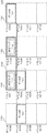
インターリーブを構成した場合、たとえば、図1に示すようなメモリ空間の利用が考えられる。図1では、バンク100〜103の4つのバンクを利用したインターリーブの例を示している。メモリ上に配置されるプログラム110が複数のバンク(バンク101、102)に跨り、且つこのプログラムによって使用されるデータ120が複数のバンク(バンク100、101、103)に跨るように配置されている。ここで例えばデータ120が、CPUやその他周辺デバイスとの間で高速アクセスを要する場合、インターリーブの特性により高速アクセスが実現可能になる。
When interleaving is configured, for example, use of a memory space as shown in FIG. 1 can be considered. FIG. 1 shows an example of interleaving using four
ここで不揮発性メモリ(例えば、MRAM)によるメモリシステムでインターリーブを構成する場合について考える。不揮発性メモリは電源オフでも記憶を維持し続ける。その為、例えば装置の特定の状態に於いてデータやプログラムの部分若しくは全体が未使用状態である場合には、未使用状態のデータ若しくはプログラムが格納されているバンクの電源を一時的に切り、必要に応じて電源供給をオンにするといった使い方が可能になる。このような電源制御は省電力に貢献することが明らかである。 Consider a case where interleaving is configured in a memory system using a nonvolatile memory (for example, MRAM). The non-volatile memory keeps storing even when the power is turned off. Therefore, for example, when the data or program part or the whole is in an unused state in a specific state of the apparatus, the bank in which the unused data or program is stored is temporarily turned off. It is possible to use such as turning on the power supply as necessary. It is clear that such power control contributes to power saving.
次にこのメモリシステムに於いて、必要に応じてバンクへの電源供給のオン・オフを切り替える場合の、より効率的なプログラム及びデータの配置方法について考える。図1は不揮発性メモリで構成されるバンク100、101、102、103から成るメモリ領域において、全てのバンクがインターリーブ構成になっている状態を示している。命令コード111、112から成るプログラム110、及びデータ片121、122、123から成るデータ120が図1のように配置されている場合を考える。この場合、不図示のCPUやその他周辺デバイスからのデータ120に対するアクセスが一時的に無い状態の時には、データ120の格納バンクに関しては電源オフにして電力を削減することができる。
Next, in this memory system, a more efficient program and data arrangement method will be considered when the power supply to the bank is switched on and off as necessary. FIG. 1 shows a state in which all banks are in an interleave configuration in a memory area composed of
このとき、バンク100及び103に配置されているのは夫々データ片122、121のみでありプログラム110の命令コードのいずれも含まれていない。その為、一時的にデータ120へのアクセスが無い場合にこれらバンク100、103の電源をオフにしてもプログラム110の実行に支障は無い。しかしながらバンク101にはデータ片123だけでなくプログラム110の命令コード111も配置されている。よって、このプログラム110の稼動中にバンク101の電源オフを実施すると、プログラム110の実行に支障をきたしてしまう為、データ120へのアクセスが無い場合でもバンク101の電源をオフにすることは出来ない。
At this time, only the
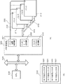
次に、本実施形態のメモリ制御装置としてのメモリアクセス装置について、図2を用いて説明する。図2(A)は本実施形態によるメモリアクセス装置を含むメモリシステム周辺の構成例を示すブロック図である。CPU200はメモリに対して読み出しや書き込みアクセスを行う中央処理回路であり、バンク210、211、212、213は不揮発性メモリから成るメモリバンクである。メモリ制御部220は、バンク210、211、212、213によって構成されるメモリ領域へのメモリアクセス制御を行なう回路である。バンク電源制御部221はバンク210、211、212、213の電源オン・オフ状態を設定するレジスタを備えた制御回路である。インターリーブ設定部222は各バンクをインターリーブ領域として扱うか、若しくは非インターリーブ領域として扱うかを設定する回路である。
Next, a memory access device as a memory control device of this embodiment will be described with reference to FIG. FIG. 2A is a block diagram showing a configuration example around the memory system including the memory access device according to the present embodiment. The
バンク電源制御線230はバンク電源制御部221からバンク210、211、212、213の夫々に接続され、バンク電源制御部221に設定された各バンクの電源オン・オフ状態を元に、各バンクの電源を制御するための信号線である。メモリバス240はメモリ制御部220とバンク210、211、212、213を接続し、メモリアクセスのためのアドレス線とデータ線及び制御線からなるバスである。システムバス250はCPU200とメモリ制御部220若しくは不図示の周辺デバイスとを接続するバスである。
The bank
図2(B)は、バンク電源制御部221が有するバンク電源制御レジスタ260を示す。バンク電源制御レジスタ260は、複数のバンクの各々について電源供給をオンするかオフするかを示す情報を保持する。この実施形態では、バンク電源制御レジスタ260は4ビットから成り、ビット0、1、2、3の夫々がバンク210、211、212、213に対応する。バンク電源制御部221は、バンク電源制御レジスタ260のビットの値が0の時はそのビットに対応するバンク電源の供給をオフに、1の時にはそのビットに対応するバンク電源の供給をオンにする。
FIG. 2B shows a bank power control register 260 included in the bank
図2(C)にインターリーブ設定部222が有するインターリーブ設定レジスタ270を示す。インターリーブ設定レジスタは、複数のバンクの各々についてインターリーブ領域と非インターリーブ領域のいずれに設定されているかを示す設定情報を保持する。この実施形態では、インターリーブ設定レジスタ270は4ビットから成り、ビット0、1、2、3の夫々がバンク210、211、212、213に対応する。インターリーブ設定部222は、インターリーブ設定レジスタ270のビットの値が0の時はそのビットに対応するバンクは非インターリーブ領域として、1の時にはそのビットに対応するバンクはインターリーブ領域としてアクセスするようアドレスを設定する。なお、インターリーブ領域、非インターリーブ領域におけるアドレスの設定は、図3(C)において詳述する。
FIG. 2C shows an
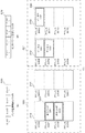
次に、図2で説明したメモリシステムで実際にインターリーブ設定を行い、且つ各バンクの電源制御を行う例を図3(A)、(B)及び(C)を用いて説明する。図3(A)は、図2(B)で説明したバンク電源制御レジスタ260のビット0〜3を全て1に設定した状態を示している。この場合、バンク電源制御部221は、バンク210〜213の全てのバンクへの電源供給をオン状態とし、全てのバンクに電源が供給されるようにする。また、図3(B)は、図2(C)で説明したインターリーブ設定レジスタ270のビット0及び1に0を、ビット2及び3に1を設定した状態を示している。この場合、バンク210、211が非インターリーブに、バンク212、213がインターリーブに設定される。
Next, an example in which the interleave setting is actually performed in the memory system described with reference to FIG. 2 and the power supply control of each bank is performed will be described with reference to FIGS. 3 (A), (B), and (C). FIG. 3A shows a state in which
更に、図3(C)は、図1の説明で示した4つの不揮発性メモリで構成されるバンク210、211、212、213から成る非インターリーブ領域及びインターリーブ領域の構成を示している。本実施形態では、インターリーブ設定レジスタ270により、バンク毎にインターリーブ、非インターリーブを設定できる。そのため、複数のバンク210〜213により構成される記憶領域のうちの一部をインターリーブ領域に、他の領域を非インターリーブ領域に設定することができる。図3(A)のバンク電源制御レジスタ260の設定に基づき、図3(C)のバンク210、211、212、213の夫々の電源がオン状態になっている。また図3(B)のインターリーブ設定レジスタ270の設定に基づき、バンク210、バンク211は非インターリーブ領域300を、またバンク211、バンク212はインターリーブ領域301を構成する。
Further, FIG. 3C shows a configuration of a non-interleaved area and an interleaved area composed of
図3(C)において、アドレス3000〜3007は非インターリーブ領域300内に割り当てられる論理アドレスであり、このアドレスはバンクを跨ぐこと無くバンク210の先頭から終端、続いてバンク211の先頭から終端の順に割り当てられる。またアドレス3008〜3015はインターリーブ領域内に割り当てられた論理アドレスであり、この論理アドレスは各バンクに交互に跨るように割り振られる。
In FIG. 3C, addresses 3000 to 3007 are logical addresses assigned in the
なお、図3の例では、バンク212とバンク213の2つがインターリーブに設定されている様子を示したが、3つ以上のバンクがインターリーブに設定されてもよい。例えば、インターリーブ設定レジスタ270のビット1〜3に1が設定されると、バンク211〜213の3つのバンクがインターリーブで動作するようになる。また、図3に示した複数のインターリーブ領域を設定できるようにしてもよい。すなわち、図3(C)において、非インターリーブ領域300をインターリーブとして設定できるようにしてもよい。その場合、インターリーブ設定レジスタ270は、インターリーブ領域を識別できるように、各バンクについて2ビット以上の深さを有するように構成される必要がある。例えば、各バンクに対応して2ビットを設ければ、「0:非インターリーブ領域」、「1:インターリーブ領域A」、「2:インターリーブ領域B」、「3:インターリーブ領域C」というように、独立したインターリーブ領域を3つまで設定することが可能となる。
In the example of FIG. 3, a state is shown in which two
図3(C)において、プログラム320は命令コード321及び命令コード322から成るプログラムコードであり、CPU200によって実行される。本実施形態ではプログラム320は非インターリーブ領域300のバンク210に配置されている。データ330はCPU200による読出しや書込みが可能なデータである。本実施形態では、バンク212及び213に跨るように格納されたデータの各部分を夫々データ片331、データ片332、データ片333とする。
In FIG. 3C, a
今、CPU200はプログラム320を実行しており、かつプログラム320はデータ330に関して読出し若しくは書込みアクセスを伴う処理を有しているものとする。データ330はインターリーブ領域301に格納されている為、CPU200からの読み出し及び書き込みに関してレイテンシの少ない高速なアクセスが可能である。
Now, it is assumed that the
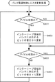
ここでCPU200が実行しているプログラム320は、図8のフローチャートで示されるバンク電源制御レジスタ260の更新処理を含む。すなわち、ステップS801において、CPU200は、実行中のプログラムからデータ330へのアクセスが発生しない状態になるのを待つ。例えば、実行中のプログラム320のメイン処理がアイドル状態(例えば、装置が省電力のための待機状態)になり、データ330に対するアクセスが無い状態になったとする。この場合、もはやインターリーブ領域301に対する一切のアクセスが発生しない為、インターリーブ領域301に含まれるバンク212及び213の電源をオフすることが可能である。したがって、データ330へのアクセスが発生しない状態になったと判定されると、処理はステップS802に進み、CPU200は、バンク電源制御レジスタ260のビット2及び3(インターリーブ領域のバンクに対応したビット)を0に書き換える。バンク電源制御レジスタ260がこのように更新されると、バンク電源制御部221は、バンク212及び213の電源をオフ状態とする。
Here, the
その後、ステップS803においてCPU200はデータ330へのアクセスが発生する状態に復帰するのを待つ。例えば、実行中のプログラム320のメイン処理がアイドル状態から通常状態に復帰すると処理はステップS804へ進む。ステップS804において、CPU200は、ステップS802で0に書き換えたビット(本例では、インターリーブ領域のバンクに対応したビット2及び3)を1に書き換える。バンク電源制御レジスタ260がこのように更新されると、バンク電源制御部221は、バンク212及び213の電源をオン状態とする。各バンクは全て不揮発性メモリである為、電源オフの状態でもインターリーブ領域301に配置されているデータ330は消える事は無い。従ってバンク電源制御レジスタ260のビット2及び3を1に書き戻すことでバンク212及び213の電源をオンにすれば、再びデータ330を読み出すことが出来る。
Thereafter, in step S803, the
なお、上記第1実施形態ではプログラムを非インターリーブ領域に、データをインターリーブ領域に配置したが、実際の利用にあたっては必ずしもこの配置に限定されるものでは無い。また本実施形態では実運用中にデータへのアクセスが不要になったケースに言及し、データが格納されているインターリーブ領域の電源をオン・オフする例を示した。しかしながら、必ずしもインターリーブ領域だけが電源オン・オフの対象に限定されるものではなく、実際の適用形態に応じて非インターリーブ領域が電源オン・オフされてもよいことは明らかである。すなわち、複数のバンクのうちの一部をインターリーブ領域、他のバンクを非インターリーブ領域として使用する構成において、インターリーブ領域を構成するバンクと非インターリーブ領域を構成するバンクとで個別に電源供給が制御されるようにすればよい。また、非インターリーブ領域への電源供給の制御は、非インターリーブ領域を構成する全てのバンクを一括して電源供給のオン、オフを行なってもよいし、非インターリーブ領域を構成する個々のバンクに対して個別に電源供給のオン、オフを行なってもよい。さらに、CPU200が非インターリーブ領域300及びインターリーブ領域301へアクセスした場合について説明しているが、必ずしもCPUからのアクセスに限定するものではない。例えばDMAコントローラ等の不図示の周辺デバイスからのアクセスであってもよい。
In the first embodiment, the program is arranged in the non-interleave area and the data is arranged in the interleave area. However, the actual use is not necessarily limited to this arrangement. Further, in the present embodiment, a case where access to data becomes unnecessary during actual operation is described, and an example of turning on / off the power of an interleave area where data is stored is shown. However, only the interleave region is not necessarily limited to the power on / off target, and it is obvious that the non-interleave region may be turned on / off according to the actual application. In other words, in a configuration in which a part of a plurality of banks is used as an interleave area and another bank is used as a non-interleave area, power supply is controlled separately for the banks constituting the interleave area and the banks constituting the non-interleave area. You can do so. In addition, the control of power supply to the non-interleaved area may be performed by turning on / off the power supply for all banks constituting the non-interleaved area at once, or for each bank constituting the non-interleaved area. The power supply may be turned on and off individually. Furthermore, although the case where the
バンク電源制御レジスタ260に関しては、各ビットの論理として0で電源オフ、1で電源オンとしたが、必ずしもこの論理に限定するものではなく、例えば0で電源オン、1で電源オフとしてもよい。同様に、インターリーブ設定レジスタ270に関しては、各ビットの論理として0で非インターリーブ設定、1でインターリーブ設定としたが、必ずしもこの論理に限定するものではなく、例えば0でインターリーブ設定、1で非インターリーブ設定としてもよい。また、本実施形では、バンク電源制御部221はメモリ制御部220に内蔵しているが、本発明はこのような形態に限られるものではなく、例えば他の周辺回路内にバンク電源制御部221が存在してもよい。
Regarding the bank
以上のように、第一実施形態によれば、インターリーブ領域と非インターリーブ領域とが混在する構成において、バンクを単位とした電源供給が適切に制御され、省電力効果を向上させることができる。 As described above, according to the first embodiment, in a configuration in which an interleave area and a non-interleave area are mixed, power supply in units of banks is appropriately controlled, and the power saving effect can be improved.
[第二実施形態]
第一実施形態では、4つのバンクから成るメモリ領域を1つの非インターリーブ領域と1つのインターリーブ領域の2つの領域に分割するケースについて述べた。第二実施形態ではメモリ領域内に2つの非インターリーブ領域と1つのインターリーブ領域が混在するケースについて説明する。以下、図2で説明したメモリシステムにおいて、2つの非インターリーブ領域を設定し、各バンクの電源制御を行う例を図4(A)、(B)及び(C)を用いて説明する。
[Second Embodiment]
In the first embodiment, a case has been described in which a memory area composed of four banks is divided into two areas, one non-interleave area and one interleave area. In the second embodiment, a case where two non-interleaved areas and one interleaved area are mixed in the memory area will be described. Hereinafter, an example in which two non-interleaved areas are set in the memory system described with reference to FIG. 2 and power control of each bank is performed will be described with reference to FIGS. 4A, 4B, and 4C.
図4(A)は、図2(B)で説明したバンク電源制御レジスタ260のビット0〜3を全て1に設定した状態を示している。図4(B)は、図2(C)で説明したインターリーブ設定レジスタ270のビット0及び3に0を、ビット1及び2に1を設定した状態を示している。図4(C)は、図1及び第一実施形態で説明したものと同じ不揮発性メモリで構成されるバンク210、211、212、213から成る非インターリーブ領域及びインターリーブ領域の構成を示している。
FIG. 4A shows a state in which
図4(C)に示されるように、図4(B)のインターリーブ設定レジスタ270の設定に基づき、バンク210は非インターリーブ領域400を、バンク211及び212はインターリーブ領域401を、またバンク213は非インターリーブ領域を構成する。また図4(A)のバンク電源制御レジスタ260の設定に基づき、バンク210、211、212、213の夫々の電源がオン状態になっている。
As shown in FIG. 4C, based on the setting of the
図4(C)において、アドレス4000〜4003は非インターリーブ領域400に、アドレス4004〜4011はインターリーブ領域401に、アドレス4012〜4015は非インターリーブ領域402に、割り当てられる論理アドレスである。ここでアドレス4004〜4011はインターリーブ領域401内のバンク211及び212に交互に跨るように割り当てられる。
In FIG. 4C, addresses 4000 to 4003 are logical addresses assigned to the
プログラム320及びデータ330は第一実施形態で説明したものと同様である。第二実施形態では、データ330はインターリーブ領域401に配置される。すなわちバンク211及び212に跨るように格納される。スタック領域413は、プログラム320によって管理され使用されるスタックメモリである。このスタック領域413は、プログラム320が実行される際の一時的な情報の退避及び参照に常時用いられる。
The
今、CPU200はプログラム320を実行しており、かつプログラム320はデータ330に対し読出し若しくは書込みアクセスを伴う処理を有しているものとする。データ330はインターリーブ領域401に格納されている為、CPU200からの読み出し及び書き込みに関してレイテンシの少ない高速なアクセスが可能である。プログラム320は、更に、図8のフローチャートにより上述した処理(バンク電源制御レジスタ260の更新処理)を実行する。その結果、以下のような動作が実現される。
Now, it is assumed that the
CPU200が実行しているプログラム320がアイドル状態になり、データ330に対するアクセスが無い状態になったとする。この場合、もはやインターリーブ領域401に対する一切のアクセスが発生しない為、インターリーブ領域401に含まれるバンク211及び212の電源をオフすることが可能である。ここでCPU200がバンク電源制御レジスタ260のビット1及び2を0に書き換えると、バンク211及び212の電源がオフ状態になる。スタック領域413は、プログラム320がアイドル動作中も常時使用されているため、バンク210同様、バンク213についても電源はオン状態を維持しておく。
It is assumed that the
以上のように、第二実施形態によれば、待機動作の実行中にアクセスが必要なプログラムやデータを非インターリーブ領域に保持し、待機動作の実行中にアクセスが不要なプログラムやデータをインターリーブ領域に保持するようにした。そのため、待機動作中においてインターリーブ領域への電源供給を停止することができ、省電力効果を向上させることができる。なお、待機動作中にアクセス可能な領域を非インターリーブ領域、待機動作中にアクセス不能な領域をインターリーブ領域としたが、これに限られるものではない。待機動作中に電源供給をオフする領域を非インターリーブ領域としてもよい。更に、図3(C)の300で示した領域をインターリーブ領域301とは独立したインターリーブ領域に設定し、それぞれのインターリーブ領域について個別に電源供給を制御するようにしてもよい。その場合、待機動作中にもアクセスの必要なプログラムやデータを高速アクセスが可能なインターリーブ領域(図3(C)の300の領域)に配置し、待機動作中も電源が供給されるように構成できる。
As described above, according to the second embodiment, programs and data that need to be accessed during execution of the standby operation are held in the non-interleave area, and programs and data that do not need to be accessed during the execution of the standby operation are stored in the interleave area. To keep. Therefore, the power supply to the interleave area can be stopped during the standby operation, and the power saving effect can be improved. In addition, although the area accessible during the standby operation is the non-interleave area and the area inaccessible during the standby operation is the interleave area, the present invention is not limited to this. A region where the power supply is turned off during the standby operation may be a non-interleaved region. Further, the area indicated by 300 in FIG. 3C may be set as an interleave area independent of the
各バンクは全て不揮発性メモリである為、電源オフの状態でもインターリーブ領域401に配置されているデータ330は消える事は無い。従ってバンク電源制御レジスタ260のビット1及び2を1に書き戻すことでバンク211及び212の電源をオンにすれば、再びデータ330を読み出すことが出来る。
Since each bank is a non-volatile memory, the
このように、一時的に動作不要なバンクについて電源オフ状態にすることで、消費電力を削減することが可能である。また不揮発性メモリである為、バンクの電源を再度オン状態にするだけで、一切の書き戻し作業を必要とせずに、バンク内の記憶を参照することができる。その為、例えば上記例のようにアイドル動作時にこの仕組みを使用するプログラムなどでは、待機動作から通常動作への状態遷移が速くなる。 In this way, it is possible to reduce power consumption by temporarily turning off a bank that does not require operation. Further, since it is a non-volatile memory, it is possible to refer to the memory in the bank without requiring any write-back operation only by turning on the bank power again. Therefore, for example, in a program that uses this mechanism during an idle operation as in the above example, the state transition from the standby operation to the normal operation becomes faster.
[第三実施形態]
第一実施形態及び第二実施形態では、各バンクへのメモリアクセス要・不要の状態に応じて、CPU200からバンク電源制御レジスタ260を書き換えることで、各バンクの電源制御を行なう方法について説明した。先の方法ではCPU200によって実行中のプログラムが、データの使用状態を把握していた。そして一時的にデータアクセスが不要になった場合には、プログラムによるソフトウェア処理(レジスタ書き換え)を行って、データを配置しているバンクを電源オフした。またデータアクセスが必要になった場合は、再度プログラムがソフトウェア処理を行って当該バンクの電源をオンするという仕組みであった。第三実施形態では各バンクの電源オン・オフ制御を、CPU200が実行するプログラムのソフトウェア処理によらずハードウェア処理で実現する方法について説明する。
[Third embodiment]
In the first embodiment and the second embodiment, the method of performing the power control of each bank by rewriting the bank power control register 260 from the
図5(A)は第三実施形態におけるメモリシステムの構成例を示すブロック図である。メモリ制御部500では、図2(A)に於けるメモリ制御部220に対し、新たにバンクアクセス監視部510が追加されている。バンクアクセス監視部510は、各バンクへのアクセスが最後に発生してから現在までどのくらいの時間が経過したか、すなわちバンクへの未アクセス時間の経過を、タイマカウンタを用いて監視する回路である。メモリ制御部500及びバンクアクセス監視部510以外の部位に関しては、第一実施形態及び第二実施形態で説明したものと同様である。
FIG. 5A is a block diagram showing a configuration example of the memory system in the third embodiment. In the
図5(B)はバンクアクセス監視部510に内蔵されたタイマ設定レジスタ520、521、522、523を示している。タイマ設定レジスタ520、521、522、523は各々バンク210、211、212、213に対応している。メモリ制御部500は、夫々のバンクへの未アクセス時間をバンクアクセス監視部510で計測しつつ、これらのレジスタのタイマ設定値と比較する。どこからもバンクへのアクセスが無く、バンク未アクセス時間がそのバンクに対応するレジスタ設定値を超えた場合は、メモリ制御部500は、バンク電源制御レジスタ260の当該バンクに対応するビットを0に設定し、当該バンクへの電源供給をオフにする。但し、第一、第二実施形態から明らかなように、インターリーブ領域に関しては個別にバンクの電源供給をオン、オフすることはできない。したがって、インターリーブ領域を構成する全てのバンクへの未アクセス時間がタイマ設定レジスタにより設定された所定時間を超えた場合に、バンク電源制御レジスタ260におけるそれらバンクのビットを0に設定する。例えば、図4(C)のような設定の場合、バンク211とバンク212における未アクセス時間がそれぞれタイマ設定レジスタ521、522に設定されている時間を超えた場合に、バンク電源制御レジスタ260のビット1とビット2が0に設定される。
FIG. 5B shows timer setting registers 520, 521, 522, and 523 built in the bank
その後、電源オフ状態のバンクに対してCPU200から読み出し若しくは書き込みアクセスがあった場合、そのバンクアクセスがバンクアクセス監視部510により検出される。バンクアクセス監視部510により電源オフ状態のバンクへのアクセスが検出されると、メモリ制御部500はバンク電源制御レジスタ260の当該バンクに対応するビットを1に設定することで、当該バンクの電源を再びオンにする。また、バンク電源制御レジスタ260の電源オフ状態であったバンクに対応するビットを1に設定するとともに、当該バンクに関わるタイマ計測処理を一旦リセットして再度計測を開始する。
Thereafter, when there is a read or write access from the
以上のように、第三実施形態によれば、メモリ制御部500内にバンクへのアクセス状態を監視する仕組みを持たせ、アクセス状態に応じて自動的にバンクへの電源供給をオン・オフするようにした。そのため、CPU200によるアクセス状態監視やプログラム制御による電源オン・オフ処理が不要になり、システムを効率化することができる。
As described above, according to the third embodiment, the
なお第三実施形態では電源供給のオン及びオフ処理の両方をバンクアクセス監視部510とバンク電源制御部221によるハードウェア制御で行っているが、必ずしもこの構成に限定するものではない。例えばバンク電源オンはCPU200によるソフトウェア処理で行い、バンク電源オフは上述したようなハードウェア制御で行ってもよい。あるいはバンク電源オンはハードウェア制御で行い、バンク電源オフはCPU200によるソフトウェア処理(例えば図8の処理)で行うようにしてもよい。
In the third embodiment, both power supply ON / OFF processing is performed by hardware control by the bank
[第四実施形態]
第四実施形態では、第一実施形態、第二実施形態及び第三実施形態で示した構成におけるメモリ領域内の任意の論理アドレスが、いずれのバンクの何処の物理アドレスに対応付けられるかを求める方法の一例について述べる。
[Fourth embodiment]
In the fourth embodiment, an arbitrary logical address in the memory area in the configuration shown in the first embodiment, the second embodiment, and the third embodiment is determined to correspond to which physical address of which bank. An example of the method will be described.
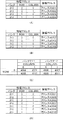
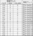
第二実施形態で説明した図4(C)を例にして説明する。まず図4(C)のバンク210、211、212及び213について夫々のバンク内の物理アドレス、すなわちROWアドレス及びCOLUMNアドレスを想定する。ここでは説明を簡便にするために各バンクともROWアドレス数が2、COLUMNアドレス数が2とする。従って各バンクはROWアドレス数×COLUMNアドレス数=4アドレス構成となる。
The description will be made with reference to FIG. 4C described in the second embodiment. First, for the
次に、非インターリーブ領域400のバンク210に割り当てられた論理アドレス4000、4001、4002及び4003と、バンク内の物理アドレスの対応付けについて考える。バンク210内の物理アドレスをバンク番号、ROWアドレス、COLUMNアドレスで表し、論理アドレスとの対応関係を整理すると、図6(A)のような対応関係になる。同様に非インターリーブ領域402内のバンク213についても、バンク番号、ROW及びCOLUMNアドレスと論理アドレスに関して、図6(B)のような対応関係が得られる。
Next, the correspondence between the
さらにインターリーブ領域401内のバンク211及び212について考える。先の図4(C)に示したように、バンク211及び212はインターリーブ領域を構成している為、論理アドレスは各バンクを跨るように交互にアドレスされる。即ちバンク211にはアドレス4004、4006、4008、4010が、またバンク212にはアドレス4005、4007、4009、4011が割り当てられる。この状態において、各バンク内のROW及びCOLUMNアドレスと論理アドレスの対応関係は図6(C)のようになる。これを論理アドレス順に再整理したものが図6(D)である。
Further, consider the
図7は、上記の図6(A)、(B)、及び(D)を論理アドレス順にひとつにまとめたテーブルであり、論理アドレスを物理アドレスにマッピングするルックアップテーブル(以下LUTと証する)である。例えばこのLUTをメモリ制御部220に内蔵すれば、CPU200若しくは不図示の周辺デバイスから発生する任意の論理アドレスを、このLUTを参照して物理アドレス(バンク番号、ROW及びCOLUMN)に変換することが出来る。
FIG. 7 is a table in which FIGS. 6A, 6B, and 6D are combined into one in the order of logical addresses, and is a lookup table (hereinafter referred to as LUT) that maps logical addresses to physical addresses. is there. For example, if this LUT is built in the
なお、実際の構成においては、上述のようにあらかじめ論理アドレスと物理アドレスの対応関係を求めておき、LUTとしてメモリ制御部220の中に内蔵してもよい。あるいは論理アドレスと物理アドレスの対応関係に算術的な規則性が存在するならば、論理アドレスから物理アドレスへ変換する演算処理によってLUTを生成してもよい。若しくはLUTそのものを持たず、メモリアクセス発生の都度、論理アドレスから物理アドレスへ変換する演算処理を動的に行って、論理アドレスと物理アドレスの対応関係を求めてもよい。本提案は、これら論理アドレスと物理アドレスの対応関係の導出の仕方について限定するものではない。
In an actual configuration, the correspondence relationship between the logical address and the physical address may be obtained in advance as described above, and may be incorporated in the
以上のように、上記実施形態によれば、高速アクセスが必要なデータやプログラムを配置するバンクと、低速アクセスでも構わないデータやプログラムを配置するバンクを完全に分離出来る。そして、分離したインターリーブ領域若しくは非インターリーブ領域の何れかが一時的にアクセス不要な場合には各領域を個別に電源オフすることが可能になり、消費電力を削減できる。 As described above, according to the above-described embodiment, it is possible to completely separate a bank in which data and programs requiring high-speed access are arranged from a bank in which data and programs that may be accessed at low speed are arranged. When either the separated interleave area or the non-interleave area is temporarily not required to access, each area can be individually powered off, and the power consumption can be reduced.
なお、上記実施形態では、MRAMを用いた構成を示したが、本発明の適用はMRAMを用いたメモリシステム限られるものではなく、不揮発性メモリを用いたメモリシステム全般において本発明は好適に適用できる。 In the above embodiment, the configuration using the MRAM is shown. However, the application of the present invention is not limited to the memory system using the MRAM, and the present invention is preferably applied to the entire memory system using the nonvolatile memory. it can.
また、上述したメモリシステムは、デジタルカメラ、ビデオカメラ、携帯電話やタブレットなどの各種情報処理装置、電子機器に用いることができ、上述したメモリシステムが適用された情報処理装置、電子機器も本発明の範疇である。 The above-described memory system can be used for various information processing apparatuses and electronic devices such as digital cameras, video cameras, mobile phones, and tablets, and information processing apparatuses and electronic devices to which the above-described memory system is applied are also included in the present invention. This is a category.
また、本発明は、以下の処理を実行することによっても実現される。即ち、上述した実施形態の機能を実現するソフトウェア(プログラム)を、ネットワーク又は各種記憶媒体を介してシステム或いは装置に供給し、そのシステム或いは装置のコンピュータ(またはCPUやMPU等)がプログラムを読み出して実行する処理である。 The present invention can also be realized by executing the following processing. That is, software (program) that realizes the functions of the above-described embodiments is supplied to a system or apparatus via a network or various storage media, and a computer (or CPU, MPU, or the like) of the system or apparatus reads the program. It is a process to be executed.
Claims (9)
複数のバンクの間でバンクインターリーブのアクセスを行う第1の領域と、バンクインターリーブのアクセスを行わない第2の領域のいずれかの領域に、前記不揮発メモリにおける複数のバンクを設定し、前記不揮発メモリへのアクセス制御を行うメモリアクセス手段と、 A plurality of banks in the nonvolatile memory are set in any one of a first area where bank interleave access is performed between a plurality of banks and a second area where bank interleave access is not performed, and the nonvolatile memory Memory access means for controlling access to
前記第1の領域のバンクと前記第2の領域のバンクとを独立に省電力状態に制御する電力制御手段とを備えることを特徴とするメモリ制御装置。 A memory control device comprising: power control means for independently controlling a bank in the first area and a bank in the second area in a power saving state.
前記第2の領域のバンクには前記CPUにより実行されるプログラムが記憶され、前記第1の領域のバンクには前記プログラムを前記CPUが実行するときに使用されるデータが記憶されることを特徴とする請求項1から4のいずれか1項に記載のメモリ制御装置。 A program executed by the CPU is stored in the bank of the second area, and data used when the CPU executes the program is stored in the bank of the first area. The memory control device according to any one of claims 1 to 4.
複数のバンクの間でバンクインターリーブのアクセスを行う第1の領域と、バンクインターリーブのアクセスを行わない第2の領域のいずれかの領域に、前記不揮発メモリにおける複数のバンクを設定し、前記不揮発メモリへのアクセス制御を行うメモリアクセス工程と、 A plurality of banks in the nonvolatile memory are set in any one of a first area where bank interleave access is performed between a plurality of banks and a second area where bank interleave access is not performed, and the nonvolatile memory A memory access process for controlling access to
前記第1の領域のバンクと前記第2の領域のバンクとを独立に省電力状態に制御する電力制御工程とを有することを特徴とするメモリ制御方法。 A memory control method comprising: a power control step of independently controlling a bank in the first area and a bank in the second area to a power saving state.
Priority Applications (2)
| Application Number | Priority Date | Filing Date | Title |
|---|---|---|---|
| JP2012161964A JP6000708B2 (en) | 2012-07-20 | 2012-07-20 | Memory control apparatus and method |
| US13/942,039 US9424174B2 (en) | 2012-07-20 | 2013-07-15 | Control apparatus and method for controlling a memory having a plurality of banks |
Applications Claiming Priority (1)
| Application Number | Priority Date | Filing Date | Title |
|---|---|---|---|
| JP2012161964A JP6000708B2 (en) | 2012-07-20 | 2012-07-20 | Memory control apparatus and method |
Publications (3)
| Publication Number | Publication Date |
|---|---|
| JP2014021859A JP2014021859A (en) | 2014-02-03 |
| JP2014021859A5 JP2014021859A5 (en) | 2015-09-03 |
| JP6000708B2 true JP6000708B2 (en) | 2016-10-05 |
Family
ID=49947539
Family Applications (1)
| Application Number | Title | Priority Date | Filing Date |
|---|---|---|---|
| JP2012161964A Expired - Fee Related JP6000708B2 (en) | 2012-07-20 | 2012-07-20 | Memory control apparatus and method |
Country Status (2)
| Country | Link |
|---|---|
| US (1) | US9424174B2 (en) |
| JP (1) | JP6000708B2 (en) |
Families Citing this family (8)
| Publication number | Priority date | Publication date | Assignee | Title |
|---|---|---|---|---|
| US9256531B2 (en) * | 2012-06-19 | 2016-02-09 | Samsung Electronics Co., Ltd. | Memory system and SoC including linear addresss remapping logic |
| JP6030987B2 (en) * | 2013-04-02 | 2016-11-24 | ルネサスエレクトロニクス株式会社 | Memory control circuit |
| US9612648B2 (en) * | 2013-08-08 | 2017-04-04 | Qualcomm Incorporated | System and method for memory channel interleaving with selective power or performance optimization |
| KR102355573B1 (en) | 2014-10-29 | 2022-01-27 | 삼성전자주식회사 | MEMORY SYSTEM AND SoC INCLUDING LINEAR REMAPPER AND ACCESS WINDOW |
| US9680570B2 (en) | 2015-04-30 | 2017-06-13 | Nistica, Inc. | Optical channel monitor for a wavelength selective switch employing a single photodiode |
| US20170109090A1 (en) * | 2015-10-16 | 2017-04-20 | Qualcomm Incorporated | System and method for page-by-page memory channel interleaving |
| JP2017151911A (en) * | 2016-02-26 | 2017-08-31 | 東芝メモリ株式会社 | Semiconductor device and control method |
| KR102589410B1 (en) * | 2017-11-10 | 2023-10-13 | 삼성전자주식회사 | Memory device and method of controlling power of the same |
Family Cites Families (10)
| Publication number | Priority date | Publication date | Assignee | Title |
|---|---|---|---|---|
| JPS5268331A (en) * | 1975-12-05 | 1977-06-07 | Hitachi Ltd | Interleaving control system of shared memory |
| US5375250A (en) * | 1992-07-13 | 1994-12-20 | Van Den Heuvel; Raymond C. | Method of intelligent computing and neural-like processing of time and space functions |
| JPH09212416A (en) * | 1995-11-30 | 1997-08-15 | Toshiba Corp | Computer system and its power managing method |
| US5960462A (en) * | 1996-09-26 | 1999-09-28 | Intel Corporation | Method and apparatus for analyzing a main memory configuration to program a memory controller |
| JP2000267986A (en) * | 1999-03-17 | 2000-09-29 | Canon Inc | Device and method for controlling memory |
| JP3963457B2 (en) | 2003-06-30 | 2007-08-22 | 株式会社東芝 | Wireless device |
| US7165165B2 (en) * | 2004-03-16 | 2007-01-16 | Intel Corporation | Anticipatory power control of memory |
| JP2008152687A (en) * | 2006-12-20 | 2008-07-03 | Matsushita Electric Ind Co Ltd | Memory controller |
| JP4643729B2 (en) * | 2009-07-09 | 2011-03-02 | 株式会社東芝 | Interleave control device, interleave control method, and memory system |
| US8245060B2 (en) * | 2009-10-15 | 2012-08-14 | Microsoft Corporation | Memory object relocation for power savings |
-
2012
- 2012-07-20 JP JP2012161964A patent/JP6000708B2/en not_active Expired - Fee Related
-
2013
- 2013-07-15 US US13/942,039 patent/US9424174B2/en active Active
Also Published As
| Publication number | Publication date |
|---|---|
| US9424174B2 (en) | 2016-08-23 |
| US20140025867A1 (en) | 2014-01-23 |
| JP2014021859A (en) | 2014-02-03 |
Similar Documents
| Publication | Publication Date | Title |
|---|---|---|
| JP6000708B2 (en) | Memory control apparatus and method | |
| US10521003B2 (en) | Method and apparatus to shutdown a memory channel | |
| US8799553B2 (en) | Memory controller mapping on-the-fly | |
| KR100860650B1 (en) | Unified memory organization for power savings | |
| US7590021B2 (en) | System and method to reduce dynamic RAM power consumption via the use of valid data indicators | |
| US9594681B2 (en) | Dynamically configurable memory | |
| JP2009211153A (en) | Memory device, information processing apparatus, and electric power controlling method | |
| WO2016209383A1 (en) | Instant restart in non volatile system memory computing systems with embedded programmable data checking | |
| JP2017138853A (en) | Information processor and program | |
| US20220334968A1 (en) | Memory card with volatile and non volatile memory space having multiple usage model configurations | |
| JP2006092169A (en) | Memory controller, memory device and control method for memory controller | |
| US20130031397A1 (en) | Information processing apparatus | |
| TW201426304A (en) | Memory control device and method | |
| JP5294304B2 (en) | Reconfigurable electronic circuit device | |
| KR20170127948A (en) | Memory module and system including the same | |
| JP5045163B2 (en) | Arithmetic processing device and control method of arithmetic processing device | |
| WO2014172078A1 (en) | A cache allocation scheme optimized for browsing applications | |
| JP2006048342A (en) | Power saving memory access control unit | |
| JP2009258925A (en) | Computer system and memory management method of computer system | |
| TWI493563B (en) | Memory managing method and electronic apparatus using the same | |
| KR101490072B1 (en) | Apparatus and method for power control of cache | |
| JP2008033379A (en) | Nonvolatile storage apparatus | |
| KR20240025293A (en) | Memory device | |
| TW201830245A (en) | Memory apparatus and operating method thereof | |
| JPH1196756A (en) | Semiconductor memory |
Legal Events
| Date | Code | Title | Description |
|---|---|---|---|
| A521 | Request for written amendment filed |
Free format text: JAPANESE INTERMEDIATE CODE: A523 Effective date: 20150713 |
|
| A621 | Written request for application examination |
Free format text: JAPANESE INTERMEDIATE CODE: A621 Effective date: 20150713 |
|
| A977 | Report on retrieval |
Free format text: JAPANESE INTERMEDIATE CODE: A971007 Effective date: 20160518 |
|
| A131 | Notification of reasons for refusal |
Free format text: JAPANESE INTERMEDIATE CODE: A131 Effective date: 20160523 |
|
| TRDD | Decision of grant or rejection written | ||
| A01 | Written decision to grant a patent or to grant a registration (utility model) |
Free format text: JAPANESE INTERMEDIATE CODE: A01 Effective date: 20160805 |
|
| A61 | First payment of annual fees (during grant procedure) |
Free format text: JAPANESE INTERMEDIATE CODE: A61 Effective date: 20160831 |
|
| R151 | Written notification of patent or utility model registration |
Ref document number: 6000708 Country of ref document: JP Free format text: JAPANESE INTERMEDIATE CODE: R151 |
|
| LAPS | Cancellation because of no payment of annual fees |